JP4208088B2 - Wireless communication apparatus and wireless communication method - Google Patents
Wireless communication apparatus and wireless communication methodDownload PDFInfo
- Publication number
- JP4208088B2 JP4208088B2JP2006098202AJP2006098202AJP4208088B2JP 4208088 B2JP4208088 B2JP 4208088B2JP 2006098202 AJP2006098202 AJP 2006098202AJP 2006098202 AJP2006098202 AJP 2006098202AJP 4208088 B2JP4208088 B2JP 4208088B2
- Authority
- JP
- Japan
- Prior art keywords
- signal
- processing unit
- unit
- power
- signal processing
- Prior art date
- Legal status (The legal status is an assumption and is not a legal conclusion. Google has not performed a legal analysis and makes no representation as to the accuracy of the status listed.)
- Expired - Fee Related
Links
Images


Classifications
- H—ELECTRICITY
- H04—ELECTRIC COMMUNICATION TECHNIQUE
- H04B—TRANSMISSION
- H04B1/00—Details of transmission systems, not covered by a single one of groups H04B3/00 - H04B13/00; Details of transmission systems not characterised by the medium used for transmission
- H04B1/38—Transceivers, i.e. devices in which transmitter and receiver form a structural unit and in which at least one part is used for functions of transmitting and receiving
- H04B1/40—Circuits
- H04B1/50—Circuits using different frequencies for the two directions of communication
- H04B1/52—Hybrid arrangements, i.e. arrangements for transition from single-path two-direction transmission to single-direction transmission on each of two paths or vice versa
- H04B1/525—Hybrid arrangements, i.e. arrangements for transition from single-path two-direction transmission to single-direction transmission on each of two paths or vice versa with means for reducing leakage of transmitter signal into the receiver
Landscapes
- Engineering & Computer Science (AREA)
- Computer Networks & Wireless Communication (AREA)
- Signal Processing (AREA)
- Noise Elimination (AREA)
- Transceivers (AREA)
- Mobile Radio Communication Systems (AREA)
Description
Translated fromJapanese本発明は、同一キャリア周波数を用いて同時に送信と受信を行う無線通信装置に関するものである。The present invention relatesto wireless communicationequipment transmit and receive simultaneously using the same carrier frequency.
従来の無線通信におけるTDD方式では、送信と受信で同一のRF(RadioFrequency)キャリア周波数を用い、送信と受信で異なる時間的な割当(タイムスロット)を用いることにより混信を防ぐが、周波数利用効率の向上を目的として、同一タイムスロットを用いて送信と受信を同時に行う方法が、下記の特許文献1により開示されている。 In the conventional TDD system in wireless communication, the same RF (Radio Frequency) carrier frequency is used for transmission and reception, and interference is prevented by using different time allocations (time slots) for transmission and reception. For the purpose of improvement, a method of simultaneously performing transmission and reception using the same time slot is disclosed in Patent Document 1 below.
この場合、サーキュレータの不完全性により送信RF信号処理部からの信号が受信RF信号処理部に漏れ込んでしまい干渉を生じる。また、アンテナから送信された送信信号が、反射・回折等の伝搬路の影響を受けて同一のアンテナで受信されることにより干渉を生じる。これらの干渉は「回り込み干渉」と呼ばれる。無線機では、当該無線機に向けて他の無線機から送信された希望信号と上記の回り込み干渉信号とが重畳された信号を用いて、希望信号を検出する必要があるが、回り込み干渉信号の電力が大きい場合、希望信号を正しく検出することができなくなる。特に、サーキュレータの不完全性に起因する回り込み干渉の影響は、アンテナから一旦送信された後に再度受信されてしまうことにより生じる回り込み干渉の影響に比較して非常に大きくなる。 In this case, the signal from the transmission RF signal processing unit leaks into the reception RF signal processing unit due to imperfection of the circulator, causing interference. In addition, interference occurs when a transmission signal transmitted from an antenna is received by the same antenna under the influence of a propagation path such as reflection and diffraction. These interferences are called “wraparound interference”. In the wireless device, it is necessary to detect the desired signal using a signal in which the desired signal transmitted from the other wireless device and the wraparound interference signal are superimposed on the wireless device. If the power is large, the desired signal cannot be detected correctly. In particular, the influence of the sneak interference caused by the imperfection of the circulator is very large compared to the effect of the sneak interference caused by being transmitted once from the antenna and then received again.
このため、特許文献1の方法では、回り込み干渉信号除去機能を有する無線通信装置を用いて、ベースバンドのデジタル領域において干渉除去を行う方法が示されている。 For this reason, the method of Patent Document 1 discloses a method of performing interference cancellation in the baseband digital domain using a wireless communication apparatus having a wraparound interference signal cancellation function.
また、これらの干渉を除去する別の無線通信装置としては、ブースタとして記載されている回り込み干渉信号除去機能を有する無線通信装置が利用可能である。下記の非特許文献1、2には、アナログ領域であるRF帯での干渉除去と、デジタル領域であるベースバンド帯での干渉除去とを同時に行うことを特徴とする無線呼出し方式用のブースタが記載され、非特許文献3にはIF帯またはベースバンド帯で干渉除去を行う地上デジタル放送用のブースタが記載され、さらに非特許文献4にはRF帯のみにおいて干渉キャンセルを行うCDMA信号用のブースタが記載されている。
しかし、上記従来技術にかかる無線通信装置は、以下に示すような問題点があった。すなわち、上記従来の無線通信装置においては、本来受信すべき希望信号と回り込み干渉信号とが重畳されたアナログ領域の信号が、回り込み干渉信号除去機能を有する無線通信装置の受信RF信号処理部において処理される。受信RF信号処理部における信号増幅部、フィルタリング部、周波数変換部(ダウンコンバート部)は、それぞれが正しく動作するための入力電力の大きさには制限値があるために、回り込み干渉信号の電力が希望信号の電力に比較して非常に大きい場合には、入力電力が上記の制限値を超えてしまい信号が飽和してしまう。その結果、信号増幅部、フィルタリング部、周波数変換部等の受信RF信号処理部内において信号波形が大きく歪んでしまう。このとき、入力電力の大きさが上記の制限値に比べて大きいほど信号飽和の影響が大きくなり、信号波形はより大きく歪んでしまう。 However, the wireless communication apparatus according to the above prior art has the following problems. That is, in the above-described conventional wireless communication device, the signal in the analog region in which the desired signal to be originally received and the wraparound interference signal are superimposed is processed in the reception RF signal processing unit of the wireless communication device having the wraparound interference signal removal function. Is done. The signal amplification unit, filtering unit, and frequency conversion unit (down-conversion unit) in the received RF signal processing unit have a limit value for the amount of input power to operate correctly. If it is very large compared to the power of the desired signal, the input power exceeds the limit value and the signal is saturated. As a result, the signal waveform is greatly distorted in the received RF signal processing unit such as the signal amplification unit, the filtering unit, and the frequency conversion unit. At this time, as the magnitude of the input power is larger than the above limit value, the influence of the signal saturation increases, and the signal waveform is distorted more greatly.
また、上記非特許文献1、2で示されるように、受信RF信号処理部の前にアナログ領域において干渉除去を行うことにより、受信RF信号処理部での信号飽和の影響を軽減することができるが、この場合においても、アナログ領域における干渉除去部が正しく動作するための入力電力の大きさに制限値があるために、当該制限値を超える信号がアナログ領域における干渉除去部に入力してしまうと信号が飽和してしまう。このような信号飽和の影響により信号波形が歪んでしまった場合、アナログ領域であるRF帯や、デジタル領域におけるベースバンド帯にて干渉除去を行っても、十分な干渉除去特性が得られないため、希望信号の検出特性が大きく劣化してしまう。 In addition, as shown in Non-Patent Documents 1 and 2, by performing interference cancellation in the analog domain before the reception RF signal processing unit, the influence of signal saturation in the reception RF signal processing unit can be reduced. However, even in this case, since there is a limit value for the magnitude of input power for the interference cancellation unit in the analog domain to operate correctly, a signal exceeding the limit value is input to the interference cancellation unit in the analog domain. And the signal is saturated. If the signal waveform is distorted due to such signal saturation, sufficient interference cancellation characteristics cannot be obtained even if interference cancellation is performed in the RF band, which is the analog domain, and the baseband band in the digital domain. Therefore, the detection characteristic of the desired signal is greatly deteriorated.
本発明は、上記問題点を解決し、同一キャリア周波数を用いて同時に送信と受信を行う無線通信において、信号飽和の影響を軽減することができる無線通信装置を提供することを目的とする。The present invention is to solve the above problems, in a radio communication transmit and receive simultaneously using the same carrier frequency, and to providea wireless communicationequipment capable of reducing the effects of signal saturation.
上記の問題点を解決するため、本発明に係る無線通信装置は、無線通信の送受信を行う無線通信装置であって、受信される信号に含まれる回り込み干渉信号電力を抑圧するために、当該受信される信号の信号電力を減衰させる回り込み干渉信号電力抑圧部と、前記回り込み干渉信号電力抑圧部から出力された信号に含まれる回り込み干渉信号を除去する、アナログ領域の回り込み干渉信号除去機能及びデジタル領域の回り込み干渉信号除去機能の少なくとも一方を有する送受信部と、を備え、送受信部は、送信ベースバンド信号処理部と受信ベースバンド信号処理部とを含むベースバンド信号処理部を有し、ベースバンド信号処理部は、受信ベースバンド信号処理部からの出力が送信ベースバンド信号処理部に入力されるよう構成されている、ことを特徴とし、送受信部によるアナログ領域の干渉除去後の出力信号を用いて受信電力変動速度を検出する受信電力変動検出部と、送受信部によるデジタル領域の干渉除去後の出力信号電力における残留干渉信号電力の比率を検出する残留干渉信号電力検出部と、受信電力変動検出部により検出された受信電力変動速度が所定の基準値以上か否か、及び、残留干渉信号電力検出部により検出された残留干渉信号電力の比率が所定の基準比率以上か否か、のうち少なくとも一方に基づいて、送信ベースバンド信号処理部からの送信の可否を決定する送信許可/不許可決定部と、をさらに備え、送信ベースバンド信号処理部は、送信許可/不許可決定部により決定された送信可否の結果に応じて、信号の送信の実行/停止を制御する、ことを特徴とする。In order to solve the above problems, a wireless communication apparatus according to the present invention is a wireless communication apparatus that performs transmission and reception of wireless communication, and receives the reception signal in order to suppress sneak interference signal power included in a received signal. a power suppressor for coupling loop interference signal attenuates the signal power of the signals, the coupling loop interference signal power to remove the coupling loop interference signal contained in the signal output from the suppression unit, the analog domain coupling loop interference signal removal function及beauty de A transmission / reception unit havingat least one of the wraparound interference signal removal functionof the digital region, and thetransmission / reception unit includes a baseband signal processing unit including a transmission baseband signal processing unit and a reception baseband signal processing unit, The band signal processing unit is configured such that the output from the reception baseband signal processing unit is input to the transmission baseband signal processing unit. A reception power fluctuation detection unit that detects a reception power fluctuation speed using an output signal after interference cancellation in the analog domain by the transmission / reception unit, and residual interference in output signal power after digital domain interference cancellation by the transmission / reception unit Residual interference signal power detection unit for detecting the ratio of signal power, whether the received power fluctuation speed detected by the received power fluctuation detection unit is equal to or higher than a predetermined reference value, and detected by the residual interference signal power detection unit A transmission permission / non-permission determination unit that determines whether transmission from the transmission baseband signal processing unit is permitted based on at least one of whether the ratio of the residual interference signal power is equal to or greater than a predetermined reference ratio. , the transmission baseband signal processor in accordance with the result of the transmission availability determined by the transmission permission / non-permission determining unit, controls the execution / stop of transmission of the signal, that And butterflies.
上記の構成により、希望信号と回り込み干渉信号とが重畳された信号の電力を、回り込み干渉信号電力抑圧部において減衰させることにより、送受信部において信号飽和の影響を軽減することができる。また、送受信部において、例えば、アナログ領域における適応干渉キャンセラを用いる場合には、当該適応干渉キャンセルでの信号飽和の影響を軽減することができる。また、送信ベースバンド信号処理部は、受信ベースバンド信号処理部から入力されたデータを用いて送信信号を生成するため、本発明に係る無線通信装置をTDD方式におけるブースタとして用いることができ、回り込み干渉信号に起因する信号飽和の影響を軽減することができる。更に、受信電力の変動速度と残留干渉信号電力の比率のうち少なくとも一方に応じて、信号送信の可否を決定することができるため、信号飽和の影響が大きく十分な干渉除去特性が得られないような状況では、送信を許可しないと決定し、信号の送信を停止することができる。このようにして、希望信号の信号検出特性の劣化を防ぐことができる。With the above configuration, the power of the signal in which the desired signal and the sneak interference signal are superimposed is attenuated by the sneak interference signal power suppression unit, so that the influence of signal saturation can be reduced in the transmission / reception unit. In addition, in the transmission / reception unit, for example, when an adaptive interference canceller in the analog domain is used, the influence of signal saturation in the adaptive interference cancellation can be reduced.Further, since the transmission baseband signal processing unit generates a transmission signal using the data input from the reception baseband signal processing unit, the wireless communication apparatus according to the present invention can be used as a booster in the TDD scheme, The influence of signal saturation caused by the interference signal can be reduced. Furthermore, since it is possible to determine whether or not signal transmission is possible according to at least one of the ratio between the fluctuation speed of the received power and the residual interference signal power, the influence of signal saturation is large, so that sufficient interference cancellation characteristics cannot be obtained. In such a situation, it can be determined that transmission is not permitted, and transmission of the signal can be stopped. In this way, it is possible to prevent deterioration of the signal detection characteristics of the desired signal.
上記の問題点を解決するため、本発明に係る無線通信装置は、無線通信の送受信を行う無線通信装置であって、受信される信号に含まれる回り込み干渉信号電力を抑圧するために、当該受信される信号の信号電力を減衰させる回り込み干渉信号電力抑圧部と、回り込み干渉信号電力抑圧部から出力された信号に含まれる回り込み干渉信号を除去する、アナログ領域の回り込み干渉信号除去機能及びデジタル領域の回り込み干渉信号除去機能の少なくとも一方を有する送受信部と、を備え、送受信部は、送信ベースバンド信号処理部と受信ベースバンド信号処理部とを含むベースバンド信号処理部を有し、ベースバンド信号処理部は、受信ベースバンド信号処理部からの出力が送信ベースバンド信号処理部に入力されるよう構成されており、送受信部は、送信RF信号処理部と受信RF信号処理部とをさらに有し、無線通信装置は、回り込み干渉信号電力抑圧部により減衰される信号電力の大きさ、送信RF信号処理部における出力電力の大きさ、受信RF信号処理部における出力電力の大きさ、及びベースバンド信号処理部における出力の大きさ、のうち少なくとも一つを対象とした制御を行う抑圧電力制御部をさらに備え、当該抑圧電力制御部は、送信RF信号処理部の出力電力の大きさ、受信RF信号処理部の出力電力の大きさ、及びベースバンド信号処理部における出力の大きさ、のうち少なくとも一つに応じて、制御を行う、ことを特徴とし、送受信部によるアナログ領域の干渉除去後の出力信号を用いて受信電力変動速度を検出する受信電力変動検出部と、送受信部によるデジタル領域の干渉除去後の出力信号電力における残留干渉信号電力の比率を検出する残留干渉信号電力検出部と、受信電力変動検出部により検出された受信電力変動速度が所定の基準値以上か否か、及び、残留干渉信号電力検出部により検出された残留干渉信号電力の比率が所定の基準比率以上か否か、のうち少なくとも一方に基づいて、送信ベースバンド信号処理部からの送信の可否を決定する送信許可/不許可決定部と、をさらに備え、送信ベースバンド信号処理部は、送信許可/不許可決定部により決定された送信可否の結果に応じて、信号の送信の実行/停止を制御する、ことを特徴とする。 In order to solve the above problems, a wireless communication apparatus according to the present invention is a wireless communication apparatus that performs transmission and reception of wireless communication, and receives the reception signal in order to suppress sneak interference signal power included in a received signal. A sneak interference signal power suppression unit for attenuating the signal power of the sneak signal, a sneak interference signal included in the signal output from the sneak interference signal power suppression unit, A transmission / reception unit having at least one of wraparound interference signal removal function, the transmission / reception unit includes a baseband signal processing unit including a transmission baseband signal processing unit and a reception baseband signal processing unit, and baseband signal processing The unit is configured so that the output from the reception baseband signal processing unit is input to the transmission baseband signal processing unit. The transmission unit further includes a transmission RF signal processing unit and a reception RF signal processing unit, and the wireless communication device is configured to reduce the magnitude of the signal power attenuated by the wraparound interference signal power suppression unit and the output power in the transmission RF signal processing unit. A suppression power control unit that performs control for at least one of the magnitude of the output power, the magnitude of the output power in the received RF signal processing unit, and the magnitude of the output in the baseband signal processing unit, The power control unit, according to at least one of the magnitude of the output power of the transmission RF signal processing unit, the magnitude of the output power of the reception RF signal processing unit, and the magnitude of the output in the baseband signal processing unit, A reception power fluctuation detection unit that detects a reception power fluctuation speed using an output signal after the interference cancellation of the analog domain by the transmission / reception unit, and a digital domain by the transmission / reception unit A residual interference signal power detection unit that detects a ratio of the residual interference signal power in the output signal power after interference cancellation, whether the received power fluctuation speed detected by the received power fluctuation detection unit is equal to or higher than a predetermined reference value, and A transmission permission for determining whether transmission from the transmission baseband signal processing unit is possible based on at least one of whether the ratio of the residual interference signal power detected by the residual interference signal power detection unit is greater than or equal to a predetermined reference ratio A transmission baseband signal processing unit that controls execution / stop of signal transmission according to a result of transmission permission / inhibition determined by the transmission permission / non-permission determination unit. It is characterized by.
上記の構成により、希望信号と回り込み干渉信号とが重畳された信号の電力を、回り込み干渉信号電力抑圧部において減衰させることにより、送受信部において信号飽和の影響を軽減することができる。また、送受信部において、例えば、アナログ領域における適応干渉キャンセラを用いる場合には、当該適応干渉キャンセルでの信号飽和の影響を軽減することができる。また、送信ベースバンド信号処理部は、受信ベースバンド信号処理部から入力されたデータを用いて送信信号を生成するため、本発明に係る無線通信装置をTDD方式におけるブースタとして用いることができ、回り込み干渉信号に起因する信号飽和の影響を軽減することができる。また、送信RF信号処理部、受信RF信号処理部、ベースバンド信号処理部といった信号処理部それぞれにより異なる許容可能な電力に応じた出力の大きさの制御が可能となるために、信号飽和の影響をさらに軽減することができる。更に、受信電力の変動速度と残留干渉信号電力の比率のうち少なくとも一方に応じて、信号送信の可否を決定することができるため、信号飽和の影響が大きく十分な干渉除去特性が得られないような状況では、送信を許可しないと決定し、信号の送信を停止することができる。このようにして、希望信号の信号検出特性の劣化を防ぐことができる。With the above configuration, the power of the signal in which the desired signal and the sneak interference signal are superimposed is attenuated by the sneak interference signal power suppression unit, so that the influence of signal saturation can be reduced in the transmission / reception unit. In addition, in the transmission / reception unit, for example, when an adaptive interference canceller in the analog domain is used, the influence of signal saturation in the adaptive interference cancellation can be reduced. Further, since the transmission baseband signal processing unit generates a transmission signal using the data input from the reception baseband signal processing unit, the wireless communication apparatus according to the present invention can be used as a booster in the TDD scheme, The influence of signal saturation caused by the interference signal can be reduced. In addition, it is possible to control the output magnitude according to the allowable power that varies depending on the signal processing unit such asthe transmission RF signal processing unit, the reception RF signal processing unit, and the baseband signal processing unit. Can be further reduced. Furthermore, since it is possible to determine whether or not signal transmission is possible according to at least one of the ratio between the fluctuation speed of the received power and the residual interference signal power, the influence of signal saturation is large, so that sufficient interference cancellation characteristics cannot be obtained. In such a situation, it can be determined that transmission is not permitted, and transmission of the signal can be stopped. In this way, it is possible to prevent deterioration of the signal detection characteristics of the desired signal.
本発明に係る無線通信装置及び無線通信方法によれば、同一キャリア周波数を用いて同時に送信と受信を行う無線通信において、信号飽和の影響を軽減することができる。 According to the wireless communication apparatus and the wireless communication method according to the present invention, it is possible to reduce the influence of signal saturation in wireless communication in which transmission and reception are performed simultaneously using the same carrier frequency.
本発明の実施形態にかかる無線通信装置について図面を参照して説明する。なお、可能な場合には、同一の部分には同一の符号を付して、重複する説明を省略する。 A wireless communication apparatus according to an embodiment of the present invention will be described with reference to the drawings. If possible, the same parts are denoted by the same reference numerals, and redundant description is omitted.
[第1実施形態]
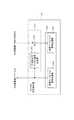
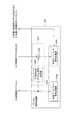
まず、本発明の第1実施形態に係る無線通信装置の構成について説明する。図1は本無線通信装置のハードウェア構成図である。無線通信装置100は、物理的には、図1に示すように、アンテナ101と、サーキュレータ102と、回り込み干渉信号電力抑圧部103と、回り込み干渉除去機能を有する送受信部104とを含んで構成される。ここで、送受信部104はアナログ信号処理部110とデジタル信号処理部120とを含んで構成され、アナログ信号処理部110はアナログ領域の干渉キャンセル部111と、受信RF信号処理部114と、送信RF信号処理部115と、A/D変換部116と、D/A変換部117とを含んで構成される。また、アナログ領域の干渉キャンセル部111は、干渉除去用アナログ信号生成部112と、アナログ領域の干渉信号除去部113とを含んで構成される。一方、デジタル信号処理部120は、入力インタフェース121と、出力インタフェース122と、CPU123と、主記憶装置であるRAM124及びROM125と、ハードディスク等の補助記憶装置126とを含んで構成される。[First Embodiment]
First, the configuration of the wireless communication apparatus according to the first embodiment of the present invention will be described. FIG. 1 is a hardware configuration diagram of the wireless communication apparatus. As shown in FIG. 1, the
本構成において、回り込み干渉信号電力抑圧部103は、アンテナ101において受信される信号に含まれる回り込み干渉信号電力を抑圧するために、当該受信される信号の信号電力を減衰させる。また、回り込み干渉除去機能を有する送受信部104は、信号電力が減衰された受信信号に含まれる回り込み干渉信号を干渉キャンセル部111において除去する。このように、回り込み干渉信号電力抑圧部103が信号電力を減衰させることにより、後続する干渉キャンセル部111における信号飽和の影響を軽減することができる。その結果、アナログ領域の回り込み干渉信号の除去特性を改善することができる。 In this configuration, wraparound interference signal
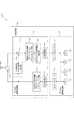
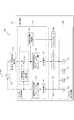
図2は本実施形態におけるデジタル信号処理部120における機能ブロック図を示す。デジタル信号処理部120は、デジタル領域の干渉キャンセル部1201とベースバンド信号処理部1204とを含んで構成され、このうち干渉キャンセル部1201は干渉除去用デジタル信号生成部1202とデジタル領域の干渉信号除去部1203とを含んで構成され、ベースバンド信号処理部1204は受信ベースバンド信号処理部1205と送信ベースバンド信号処理部1206とを含んで構成される。上記の干渉キャンセル部1201は、A/D変換部116によりデジタル信号に変換された信号に残留して含まれる回り込み干渉信号成分を除去する。このとき干渉キャンセル部1201は、送信ベースバンド信号処理部1206の出力信号を用いて干渉除去用デジタル信号生成部1202によって生成された信号を、A/D変換部116の出力信号から差し引くことにより、上記の除去を行う。ここで、アナログ信号処理部110における信号飽和の影響により、デジタル領域における回り込み干渉信号除去特性は大きく異なるが、回り込み干渉信号電力抑圧部103において信号電力を減衰させることにより、デジタル領域の回り込み干渉信号の除去特性を改善することができる。 FIG. 2 is a functional block diagram of the digital
続いて、本実施形態にかかる無線通信装置の動作及び無線通信方法について説明する。図3は、本実施形態にかかる無線通信装置において送受信を行う手順を示す図である。 Subsequently, the operation of the wireless communication apparatus and the wireless communication method according to the present embodiment will be described. FIG. 3 is a diagram illustrating a procedure for performing transmission / reception in the wireless communication apparatus according to the present embodiment.
送信ベースバンド信号処理部1206は、図3のステップS100において、送信を行う信号を発生する。送信ベースバンド信号処理部1206の出力は、干渉除去用デジタル信号生成部1202に入力されるとともに、D/A変換部117に入力される。D/A変換部117に入力された信号は、ステップS101においてアナログ信号に変換され送信RF信号処理部115に入力される。その後、ステップS102において、送信RF信号処理部115において、アンプによる信号増幅、フィルタによる帯域制限、アップコンバータによる周波数変換によりRF帯のアナログ信号に変換され、変換後の信号が、干渉除去用アナログ信号生成部112に入力されるとともに、サーキュレータ102に入力される。サーキュレータ102に入力された信号は、ステップS103において、アンテナ101を介して送信される。ここで、サーキュレータ102のアイソレーション特性の不完全性により、サーキュレータ102に入力された信号の一部は、回り込み干渉信号電力抑圧部103に供給されてしまい回り込み干渉信号となる。当該無線機100に向けて他の無線機から送信された希望信号と、ステップS103により送信された信号の回り込み干渉信号が、アンテナ101により受信され、ステップS104によって回り込み干渉信号抑圧部103に供給される。回り込み干渉信号電力抑圧部103は、アナログ信号処理部110における信号の飽和の影響を軽減するために、ステップS105において信号電力を減衰させた後に、アナログ領域の干渉信号除去部113に信号を入力する。アナログ領域の干渉信号除去部113は、ステップS106において干渉除去用アナログ信号生成部112において生成された信号を用いて、ステップS107において干渉除去を行う。ここで、干渉除去用アナログ信号生成部112は、ステップS102において生成された送信RF信号処理部115の出力信号を用いて干渉除去用のアナログ信号を生成する。アナログ領域における干渉除去後の信号は受信RF信号処理部114に入力され、受信RF信号処理部114は、ステップS108においてアンプによる信号増幅、フィルタによる帯域制限、ダウンコンバータによる周波数変換等を行う。ステップS108の処理後の信号は、その後、A/D変換部116に入力され、ステップS109において、A/D変換部116によってデジタル信号に変換され、変換後の信号は、デジタル領域の干渉信号除去部1203に入力される。デジタル領域の干渉信号除去部1203は、ステップS110において干渉除去用デジタル信号生成部1202により生成された信号を用いて、ステップS111において干渉除去を行う。ここで、干渉除去用デジタル信号生成部1202は、ステップS100において送信ベースバンド信号処理部1206において生成された信号を用いて、デジタル領域における干渉除去用の信号を発生させる。デジタル領域の干渉信号除去部1203により干渉除去が行われた信号は、ステップS112において受信ベースバンド信号処理部1205に入力され、希望信号の検出が行われる。 The transmission baseband
上述のように、ステップS105において回り込み干渉信号電力を抑圧するために信号電力を減衰させることで、ステップS107におけるアナログ領域における回り込み干渉信号の除去、及びステップS111におけるデジタル領域における回り込み干渉信号の除去における信号飽和の影響を軽減する。 As described above, the signal power is attenuated in order to suppress the sneak interference signal power in step S105, thereby removing the sneak interference signal in the analog domain in step S107 and the sneak interference signal in the digital domain in step S111. Reduce the effects of signal saturation.
ここで、上記では、受信された信号における回り込み干渉信号電力を抑圧させるために、受信時に信号電力を減衰される方法を示したが、希望信号の送信信号を増大させることで、相対的に回り込み干渉信号電力を抑圧させることができるため、ステップS105は、希望信号の送信信号を増大させることとしてもよい。 Here, in the above description, a method in which the signal power is attenuated at the time of reception is shown in order to suppress the sneak interference signal power in the received signal. Since the interference signal power can be suppressed, step S105 may increase the transmission signal of the desired signal.
続いて、本実施形態にかかる無線通信装置100の効果について説明する。本実施形態にかかる無線通信装置においては、回り込み干渉信号電力抑圧部103が信号電力を減衰させることにより、アナログ領域における干渉キャンセラ111及び受信RF信号処理部114が受ける、回り込み干渉信号に起因して生じる信号飽和の影響を軽減することができる。 Next, effects of the
以下、上述の無線通信装置の構成の変形例について説明する。上述の無線通信装置構成の例では、図1に示されるように、回り込み干渉信号電力抑圧部103が、サーキュレータ102と干渉キャンセル部111の間に設けられる構成について説明したが、図4に示すように、回り込み干渉信号電力抑圧部103が干渉キャンセル部111と受信RF信号処理部114の間に設けられる構成としても良い。この場合、回り込み干渉信号電力抑圧部103は、干渉キャンセル部111において回り込み干渉信号が除去された信号の電力を減衰させることにより、後続する受信RF信号処理部114及びA/D変換部116における信号飽和の影響を軽減することができる。 Hereinafter, modified examples of the configuration of the above-described wireless communication device will be described. In the above-described example of the wireless communication device configuration, as shown in FIG. 1, the configuration in which the wraparound interference signal
また、図5に示すように、回り込み干渉信号電力抑圧部103が、受信RF信号処理部114とA/D変換部116の間に設けられる構成としても良い。この場合も同様に、回り込み干渉信号電力抑圧部103が信号電力を減衰させることにより、A/D変換部116が受ける信号飽和の影響を軽減することができる。同様にして、回り込み干渉信号電力抑圧部103は受信RF信号処理部114内における任意の箇所に設けてもよい。 In addition, as shown in FIG. 5, the wraparound interference signal
以上のように、無線通信装置100の構成において、回り込み干渉信号電力抑圧部103を、サーキュレータ102とA/D変換部116の間のいずれかの箇所に設けることで、信号飽和の影響を軽減させることができる。 As described above, in the configuration of the
さらに、同様にして、上述の無線通信用送受信方法においては、図3に示すように、ステップS104により回り込み信号電力抑圧部103に供給された信号を対象として、ステップS105にて信号電力を減衰させる方法について説明したが、図6に示すように、ステップS107においてアナログ領域の干渉除去が行われた信号を対象として、ステップS105にて信号電力を減衰させても良い。これにより、ステップS108以降における信号飽和の影響を軽減することができる。 Further, similarly, in the above-described transmission / reception method for wireless communication, as shown in FIG. 3, the signal power is attenuated in step S105 for the signal supplied to the sneak signal
また、図7に示すように、ステップS108において受信RF信号処理後の信号を対象として、ステップS105にて信号電力を減衰させても良い。これにより、A/D変換(ステップS109)に対する信号飽和の影響を軽減することができる。同様にして、ステップS105による信号電力の減衰処理は、ステップS108における受信RF信号処理内のいずれかの段階で行うこととしても良い。 Also, as shown in FIG. 7, the signal power may be attenuated in step S105 for the signal after reception RF signal processing in step S108. Thereby, the influence of signal saturation on A / D conversion (step S109) can be reduced. Similarly, the signal power attenuation processing in step S105 may be performed at any stage in the reception RF signal processing in step S108.
以上のように、本無線通信方法において、ステップS105による信号電力の減衰処理は、ステップS104とステップS109の間のいずれかにおいて実行することにより、信号飽和の影響を軽減することができる。 As described above, in this wireless communication method, the signal power attenuation process in step S105 can be performed in any one of steps S104 and S109, thereby reducing the influence of signal saturation.
[第2実施形態]
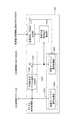
続いて、本発明の第2実施形態に係る無線通信装置の構成について説明する。本実施形態における無線通信装置の構成は、図1に示される第1実施形態における無線通信装置の構成と同一であるが、本実施形態では、デジタル信号処理部120における機能ブロックが第1実施形態とは異なる。本実施形態のデジタル信号処理部120における機能ブロック図を図8に示す。本実施形態では、ベースバンド信号処理部1204は、受信ベースバンド信号処理部1205における出力信号を、送信ベースバンド信号処理部1206の入力信号として用いる。[Second Embodiment]
Next, the configuration of the wireless communication apparatus according to the second embodiment of the present invention will be described. The configuration of the wireless communication apparatus in the present embodiment is the same as the configuration of the wireless communication apparatus in the first embodiment shown in FIG. 1, but in this embodiment, the functional blocks in the digital
第2実施形態における無線通信装置の動作について説明する。図9は第2実施形態にかかる無線通信装置において送受信を行う手順を示す図である。上述のように、ベースバンド信号処理部1204は、ステップS200において、受信ベースバンド信号処理部1205における出力信号を、送信ベースバンド信号処理部1206の入力信号として用いる。これにより、無線通信装置200をTDD方式におけるブースタとして用いることができ、回り込み干渉信号電力抑圧部103が信号を減衰させることにより、TDD方式のブースタとして無線通信装置200を用いた場合における問題点、即ち、回り込み干渉信号に起因して生じる信号飽和の影響を低減することができる。 The operation of the wireless communication apparatus in the second embodiment will be described. FIG. 9 is a diagram illustrating a procedure for performing transmission / reception in the wireless communication apparatus according to the second embodiment. As described above, the baseband
[第3実施形態]
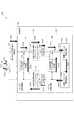
続いて、本発明の第3実施形態に係る無線通信装置の構成について説明する。本実施形態における無線通信装置のハードウェア構成を図10に示す。本実施形態における無線通信装置300は、図1に示される第1実施形態における無線通信装置100の構成に、抑圧電力制御部301をさらに備えることを特徴とする。本構成において抑圧電力制御部301は、現在の受信RF信号処理部114の出力、現在の送信RF信号処理部115の出力、現在のデジタル信号処理部120の出力、の少なくとも一つに応じて、回り込み干渉信号電力抑圧部103における信号の減衰量、受信RF信号処理部114における出力信号の大きさ、送信RF信号処理部115における出力信号の大きさ、デジタル信号処理部120における出力の大きさの少なくとも一つ制御する。[Third Embodiment]
Next, the configuration of the wireless communication apparatus according to the third embodiment of the present invention will be described. FIG. 10 shows a hardware configuration of the wireless communication apparatus according to this embodiment. The
本実施形態におけるデジタル信号処理部120の機能ブロック図について図11に示す。デジタル信号処理部120の構成は、第1実施形態と同等であるが、ベースバンド信号処理部1204の出力が、抑圧電力制御部301に入力され、抑圧電力制御部301は制御後にベースバンド信号処理部1204が適用する出力の大きさを決定し、その結果に基づいて、ベースバンド信号処理部1204は送信ベースバンド信号処理部1206の出力の大きさを制御する点が、第1実施形態とは異なる。 A functional block diagram of the digital
続いて、本実施形態にかかる無線通信装置300の動作及び無線通信方法について説明する。図12は、本実施形態にかかる無線通信装置300において送受信を行う手順を示す図である。 Subsequently, the operation of the
本実施形態にかかる無線通信用送受信方法は、第1実施形態で示される図3の手順に加えて、ステップS300〜S302、S310〜S312、S320、S321を備えることを特徴とする。 The wireless communication transmission / reception method according to the present embodiment includes steps S300 to S302, S310 to S312, S320, and S321 in addition to the procedure of FIG. 3 shown in the first embodiment.
まず、ステップS300では、送信RF信号処理部115における現在の出力信号の大きさが抑圧電力制御部301に入力されると同時に、ステップS301において、受信RF信号処理部114における現在の出力信号の大きさが抑圧電力制御部301に入力され、ステップS302において、ベースバンド信号処理1204における送信ベースバンド信号処理部1206の出力の大きさが抑圧電力制御部301に入力される。 First, in step S300, the current output signal size in the transmission RF
抑圧電力制御部301は、ステップS320において、信号飽和の影響を軽減するための、回り込み干渉信号電力抑圧部103における信号の減衰量、送信RF信号処理部115の出力信号の大きさ、受信RF信号処理部114の出力信号の大きさ、ベースバンド信号処理部1204の出力の大きさを決定する。そして、抑圧電力制御部301は、上記決定された信号減衰量を回り込み干渉信号電力抑圧部103に通知する(ステップS321)とともに、決定された出力の大きさを、送信RF信号処理部115と受信RF信号処理部114とベースバンド信号処理部1204のそれぞれに通知する(ステップS310、S311、S312)。その後、回り込み干渉信号電力抑圧部103は、上記通知された値を用いて信号を減衰させるとともに、送信RF信号処理部115、受信RF信号処理部114、ベースバンド信号処理部1204の各々は、上記通知された出力の大きさで信号を出力する。 In step S320, the suppression
なお、ここで、ステップS300〜S302について、上述ではステップS300〜S302の全てが実行される例について示したが、ステップS300〜S302のうち少なくとも一つのステップが実行されれば良い。また、ステップS310〜S312、S321についても同様に、これら全てのステップが実行される例について示したが、ステップS310〜S312、S321のうち少なくとも一つのステップが実行されれば良い。 Here, as for steps S300 to S302, the example in which all of steps S300 to S302 are executed has been described above, but at least one of steps S300 to S302 may be executed. Similarly, with respect to steps S310 to S312, S321, an example in which all these steps are executed has been described. However, at least one of steps S310 to S312, S321 may be executed.
以上により、アナログ領域の各信号処理部によって異なる許容可能な電力に応じた出力電力の大きさの制御が可能となるために、信号飽和の影響をさらに軽減することができる。 As described above, since it is possible to control the magnitude of the output power corresponding to the allowable power that varies depending on each signal processing unit in the analog domain, it is possible to further reduce the influence of signal saturation.
[第4実施形態]
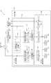
続いて、本発明の第4実施形態に係る無線通信装置の構成について説明する。本実施形態における無線通信装置のハードウェア構成を図13に示す。本実施形態における無線通信装置400は、図1に示される第1実施形態における無線通信装置100の構成に、受信電力変動検出部401をさらに備えることを特徴とする。本構成において受信電力変動検出部401は、受信電力の変動速度を検出する機能を有する。これは、受信電力の変動が速い場合には良好な干渉除去特性が得られないために、無線装置400からの信号送信を停止させることを目的とする。受信電力変動検出部401の出力は、デジタル信号処理部120に入力され、デジタル信号処理部120によって信号送信の可否が決定される。[Fourth Embodiment]
Next, the configuration of the wireless communication apparatus according to the fourth embodiment of the present invention will be described. FIG. 13 shows a hardware configuration of the wireless communication apparatus according to this embodiment. The
本実施形態におけるデジタル信号処理部120の機能ブロック図を図14に示す。デジタル信号処理部120の構成は、図2に示される第1実施形態における機能ブロックに加えて、残留干渉信号電力検出部410と送信許可/不許可決定部411とをさらに含んで構成されることを特徴とする。残留干渉信号電力検出部410は、デジタル領域の干渉除去後の出力信号における残留干渉信号の電力の比率を検出する。残留干渉信号電力検出部410により検出された残留干渉信号の電力の比率は、送信許可/不許可決定部411に入力される。送信許可/不許可決定部411は、受信電力変動検出部401により検出された受信電力変動速度が所定の基準値以上か否か、及び、残留干渉信号電力検出部410により検出された残留干渉信号の電力の比率が所定の基準比率以上か否かに基づいて、送信ベースバンド信号処理部1206から信号送信を行うか行わないかを決定し、その結果をベースバンド信号処理部1204に入力する。 A functional block diagram of the digital
続いて、本実施形態にかかる無線通信装置400の動作及び無線通信方法について説明する。図15は、本実施形態にかかる無線通信装置において送受信を行う手順を示す図である。 Subsequently, the operation of the
本実施形態にかかる手順は、第1実施形態で示される図3の手順に加えて、ステップS400〜S402をさらに備えることを特徴とする。ステップS400ではS107において、アナログ領域の干渉除去が行われた信号を用いて受信電力の変動速度を検出する。ここで、ステップS400における受信電力の変動速度の検出時においては、アナログ領域の干渉除去前の信号を用いても良いし、受信RF信号処理部114内の各処理におけるどの段階の信号を用いても良い。 The procedure according to this embodiment is characterized by further comprising steps S400 to S402 in addition to the procedure of FIG. 3 shown in the first embodiment. In step S400, the fluctuation speed of the received power is detected using the signal from which the interference of the analog area has been removed in S107. Here, at the time of detecting the fluctuation speed of the received power in step S400, a signal before removing the interference in the analog region may be used, or any stage signal in each process in the received RF
次に、ステップS401においては、デジタル領域の干渉除去後の出力信号から、残留干渉信号電力検出部410において、残留する残留干渉信号の電力を検出し、上記デジタル領域の干渉除去後の出力信号における残留干渉信号の電力比率を検出する。 Next, in step S401, the residual interference signal
そして、S402では、送信許可/不許可決定部411が、ステップS400により検出された受信電力変動速度が所定の基準値以上か否かを判断するとともに、S401により検出された残留干渉信号の電力比率が所定の基準比率以上か否かを判断する。ここで、送信許可/不許可決定部411は、受信電力変動速度が所定の基準値以上であるか、又は、残留干渉信号の電力比率が所定の基準比率以上である場合、送信ベースバンド信号処理部1206からの送信は不可と決定し、受信電力変動速度が所定の基準値未満であり、且つ、残留干渉信号の電力比率が所定の基準比率未満である場合、送信ベースバンド信号処理部1206からの送信は可能と決定する。そして、送信許可/不許可決定部411は、当該決定結果をベースバンド信号処理部1204に出力する。 In S402, transmission permission /
上記の動作を行うことにより、受信電力変動速度が所定の基準値以上に高い場合、及び、残留干渉信号の電力比率が所定の基準比率以上に高い場合に、無線通信装置400からの送信を停止するよう制御できる。これにより、信号飽和の影響を軽減し、受信ベースバンド信号処理部1205における希望信号の検出特性を改善することができる。 Performing the above operation stops transmission from
100…無線通信装置、101…アンテナ、102…サーキュレータ、103…回り込み干渉信号電力抑圧部、104…送受信部、110…アナログ信号処理部、111…干渉キャンセル部、112…干渉除去用アナログ信号生成部、113…アナログ領域の干渉信号除去部、114…受信RF信号処理部、115…送信RF信号処理部、116…A/D変換部、117…D/A変換部、120…デジタル信号処理部、121…入力インタフェース、122…出力インタフェース、123…CPU、124…RAM、125…ROM、126…HD、200…無線通信装置、300…無線通信装置、301…抑圧電力制御部、302…入出力インタフェース、400…無線通信装置、401…受信電力変動検出部、402…入力インタフェース、410…残留干渉信号電力検出部、411…送信許可/不許可決定部、1201…干渉キャンセル部、1202…干渉除去用デジタル信号生成部、1203…干渉信号除去部、1204…ベースバンド信号処理部、1205…受信ベースバンド信号処理部、1206…送信ベースバンド信号処理部。 DESCRIPTION OF
Claims (2)
Translated fromJapanese受信される信号に含まれる回り込み干渉信号電力を抑圧するために、当該受信される信号の信号電力を減衰させる回り込み干渉信号電力抑圧部と、
前記回り込み干渉信号電力抑圧部から出力された信号に含まれる回り込み干渉信号を除去する、アナログ領域の回り込み干渉信号除去機能及びデジタル領域の回り込み干渉信号除去機能の少なくとも一方を有する送受信部と、を備え、
前記送受信部は、送信ベースバンド信号処理部と受信ベースバンド信号処理部とを含むベースバンド信号処理部を有し、
前記ベースバンド信号処理部は、前記受信ベースバンド信号処理部からの出力が前記送信ベースバンド信号処理部に入力されるよう構成されている、ことを特徴とし、
前記送受信部によるアナログ領域の干渉除去後の出力信号を用いて受信電力変動速度を検出する受信電力変動検出部と、
前記送受信部によるデジタル領域の干渉除去後の出力信号電力における残留干渉信号電力の比率を検出する残留干渉信号電力検出部と、
前記受信電力変動検出部により検出された受信電力変動速度が所定の基準値以上か否か、及び、前記残留干渉信号電力検出部により検出された残留干渉信号電力の比率が所定の基準比率以上か否か、のうち少なくとも一方に基づいて、前記送信ベースバンド信号処理部からの送信の可否を決定する送信許可/不許可決定部と、をさらに備え、
前記送信ベースバンド信号処理部は、前記送信許可/不許可決定部により決定された送信可否の結果に応じて、信号の送信の実行/停止を制御する、
ことを特徴とする無線通信装置。A wireless communication device that transmits and receives wireless communication,
In order to suppress the sneak interference signal power included in the received signal, a sneak interference signal power suppression unit that attenuates the signal power of the received signal;
Removing coupling loop interference signal contained in a signal output from the power suppressor for coupling loop interference signal, a transceiver having atleast one of the coupling loop interference signal removal function of the coupling loop interference signal removal function及beauty digital region of the analog domain, With
The transceiver unit includes a baseband signal processing unit including a transmission baseband signal processing unit and a reception baseband signal processing unit,
The baseband signal processing unit is configured such that an output from the reception baseband signal processing unit is input to the transmission baseband signal processing unit,
A received power fluctuation detecting unit that detects a received power fluctuation speed using an output signal after removing interference in the analog region by the transceiver; and
A residual interference signal power detection unit for detecting a ratio of residual interference signal power in output signal power after interference cancellation in the digital domain by the transmission / reception unit;
Whether the received power fluctuation speed detected by the received power fluctuation detection unit is greater than or equal to a predetermined reference value, and whether the ratio of the residual interference signal power detected by the residual interference signal power detection unit is greater than or equal to a predetermined reference ratio A transmission permission / non-permission determination unit that determines whether transmission from the transmission baseband signal processing unit is possible based on at least one of
The transmission baseband signal processing unit controls execution / stop of signal transmission according to a result of transmission permission / inhibition determined by the transmission permission / non-permission determination unit.
A wireless communication apparatus.
受信される信号に含まれる回り込み干渉信号電力を抑圧するために、当該受信される信号の信号電力を減衰させる回り込み干渉信号電力抑圧部と、
前記回り込み干渉信号電力抑圧部から出力された信号に含まれる回り込み干渉信号を除去する、アナログ領域の回り込み干渉信号除去機能及びデジタル領域の回り込み干渉信号除去機能の少なくとも一方を有する送受信部と、を備え、
前記送受信部は、送信ベースバンド信号処理部と受信ベースバンド信号処理部とを含むベースバンド信号処理部を有し、
前記ベースバンド信号処理部は、前記受信ベースバンド信号処理部からの出力が前記送信ベースバンド信号処理部に入力されるよう構成されており、
前記送受信部は、送信RF信号処理部と受信RF信号処理部とをさらに有し、
前記無線通信装置は、前記回り込み干渉信号電力抑圧部により減衰される信号電力の大きさ、前記送信RF信号処理部における出力電力の大きさ、前記受信RF信号処理部における出力電力の大きさ、及び前記ベースバンド信号処理部における出力の大きさ、のうち少なくとも一つを対象とした制御を行う抑圧電力制御部をさらに備え、
当該抑圧電力制御部は、前記送信RF信号処理部の出力電力の大きさ、前記受信RF信号処理部の出力電力の大きさ、及び前記ベースバンド信号処理部における出力の大きさ、のうち少なくとも一つに応じて、前記制御を行う、ことを特徴とし、
前記送受信部によるアナログ領域の干渉除去後の出力信号を用いて受信電力変動速度を検出する受信電力変動検出部と、
前記送受信部によるデジタル領域の干渉除去後の出力信号電力における残留干渉信号電力の比率を検出する残留干渉信号電力検出部と、
前記受信電力変動検出部により検出された受信電力変動速度が所定の基準値以上か否か、及び、前記残留干渉信号電力検出部により検出された残留干渉信号電力の比率が所定の基準比率以上か否か、のうち少なくとも一方に基づいて、前記送信ベースバンド信号処理部からの送信の可否を決定する送信許可/不許可決定部と、をさらに備え、
前記送信ベースバンド信号処理部は、前記送信許可/不許可決定部により決定された送信可否の結果に応じて、信号の送信の実行/停止を制御する、
ことを特徴とする無線通信装置。A wireless communication device that transmits and receives wireless communication,
In order to suppress the sneak interference signal power included in the received signal, a sneak interference signal power suppression unit that attenuates the signal power of the received signal;
A transmitter / receiver having at least one of an analog domain sneak interference signal removal function and a digital domain sneak interference signal removal function, which removes a sneak interference signal included in the signal output from the sneak interference signal power suppression unit. ,
The transceiver unit includes a baseband signal processing unit including a transmission baseband signal processing unit and a reception baseband signal processing unit,
The baseband signal processing unit is configured such that an output from the reception baseband signal processing unit is input to the transmission baseband signal processing unit,
The transceiver unit further includes a transmission RF signal processing unit and a reception RF signal processing unit,
The radio communication apparatus is configured such that the magnitude of signal power attenuated by the sneak interference signal power suppression unit, the magnitude of output power in the transmission RF signal processing unit, the magnitude of output power in the reception RF signal processing unit, and A suppression power control unit that performs control for at least one of the magnitudes of outputs in the baseband signal processing unit;
The suppression power control unit includes at least one of the magnitude of output power of the transmission RF signal processing unit, the magnitude of output power of the reception RF signal processing unit, and the magnitude of output of the baseband signal processing unit. The control is performed accordingto the
A received power fluctuation detecting unit that detects a received power fluctuation speed using an output signal after removing interference in the analog region by the transceiver; and
A residual interference signal power detection unit for detecting a ratio of residual interference signal power in output signal power after interference cancellation in the digital domain by the transmission / reception unit;
Whether the received power fluctuation speed detected by the received power fluctuation detection unit is greater than or equal to a predetermined reference value, and whether the ratio of the residual interference signal power detected by the residual interference signal power detection unit is greater than or equal to a predetermined reference ratio A transmission permission / non-permission determination unit that determines whether transmission from the transmission baseband signal processing unit is possible based on at least one of
The transmission baseband signal processing unit controls execution / stop of signal transmission according to a result of transmission permission / inhibition determined by the transmission permission / non-permission determination unit.
Radio communications deviceyouwherein a.
Priority Applications (5)
| Application Number | Priority Date | Filing Date | Title |
|---|---|---|---|
| JP2006098202AJP4208088B2 (en) | 2006-03-31 | 2006-03-31 | Wireless communication apparatus and wireless communication method |
| EP07006605AEP1841084B8 (en) | 2006-03-31 | 2007-03-29 | Radio communication apparatus and radio communication method |
| DE602007010526TDE602007010526D1 (en) | 2006-03-31 | 2007-03-29 | Radio communication device and radio communication method |
| US11/694,124US7848711B2 (en) | 2006-03-31 | 2007-03-30 | Radio communication apparatus and radio communication method |
| CNA2007100922396ACN101047439A (en) | 2006-03-31 | 2007-04-02 | Radio communication apparatus and radio communication method |
Applications Claiming Priority (1)
| Application Number | Priority Date | Filing Date | Title |
|---|---|---|---|
| JP2006098202AJP4208088B2 (en) | 2006-03-31 | 2006-03-31 | Wireless communication apparatus and wireless communication method |
Publications (2)
| Publication Number | Publication Date |
|---|---|
| JP2007274390A JP2007274390A (en) | 2007-10-18 |
| JP4208088B2true JP4208088B2 (en) | 2009-01-14 |
Family
ID=38179964
Family Applications (1)
| Application Number | Title | Priority Date | Filing Date |
|---|---|---|---|
| JP2006098202AExpired - Fee RelatedJP4208088B2 (en) | 2006-03-31 | 2006-03-31 | Wireless communication apparatus and wireless communication method |
Country Status (5)
| Country | Link |
|---|---|
| US (1) | US7848711B2 (en) |
| EP (1) | EP1841084B8 (en) |
| JP (1) | JP4208088B2 (en) |
| CN (1) | CN101047439A (en) |
| DE (1) | DE602007010526D1 (en) |
Families Citing this family (26)
| Publication number | Priority date | Publication date | Assignee | Title |
|---|---|---|---|---|
| US8526903B2 (en)* | 2008-03-11 | 2013-09-03 | Qualcomm, Incorporated | High-linearity receiver with transmit leakage cancellation |
| JP5125988B2 (en)* | 2008-10-23 | 2013-01-23 | 富士通株式会社 | Wireless relay device |
| US8849335B2 (en)* | 2008-11-25 | 2014-09-30 | At&T Intellectual Property I, L.P. | Adaptive SINR control |
| RU2493648C2 (en)* | 2008-12-01 | 2013-09-20 | РОКСТАР КОНСОРЦИУМ ЮЭс ЛП | Method for frequency-dependent suppression of signals and apparatus for realising said method (versions) |
| KR101301298B1 (en)* | 2009-11-30 | 2013-08-28 | 포항공과대학교 산학협력단 | Rf relay of full-duplex and method for reducing interference of em-level thereof |
| US8285217B1 (en)* | 2010-02-16 | 2012-10-09 | The United States Of America As Represented By The Secretary Of The Navy | Circulator-enabled signal suppressor (CENSOR) for reducing co-site transmission interference |
| US9317162B2 (en)* | 2011-06-02 | 2016-04-19 | Mediatek Inc. | Apparatus and method for protecting touch panel device from noise interference |
| US9088340B2 (en) | 2011-12-21 | 2015-07-21 | Mitsubishi Electric Corporation | Wireless communication apparatus |
| CN102594463B (en)* | 2012-02-16 | 2014-09-17 | 电子科技大学 | Method and device for simultaneous common-frequency work of a plurality of pieces of electromagnetic equipment in single carrier |
| CN103916148B (en) | 2013-01-05 | 2016-08-03 | 华为技术有限公司 | A kind of adaptive RF Interference Cancellation device, method, receiver and communication system |
| EP2814184B1 (en)* | 2013-06-14 | 2018-08-08 | Alcatel Lucent | Two stage leakage cancellation in full duplex communication |
| US9184775B2 (en) | 2013-07-03 | 2015-11-10 | Raytheon Company | Methods and apparatus for adaptive nonlinear coincident interference cancellation |
| WO2015031830A1 (en)* | 2013-08-29 | 2015-03-05 | Kumu Networks, Inc. | Full-duplex relays |
| CN105393458B (en)* | 2013-10-22 | 2019-07-09 | 华为技术有限公司 | A kind of interference cancellation method and device |
| WO2015061963A1 (en)* | 2013-10-29 | 2015-05-07 | 华为技术有限公司 | Digital interference cancellation apparatus and method for wireless full duplex system and transceiver |
| WO2016073940A1 (en)* | 2014-11-06 | 2016-05-12 | GM Global Technology Operations LLC | Dynamic range of wideband rf front end using delta sigma converters with envelope tracking and injected digitally equalized transmit signal |
| US9923658B2 (en)* | 2014-12-23 | 2018-03-20 | Intel Corporation | Interference cancelation |
| WO2016128048A1 (en)* | 2015-02-12 | 2016-08-18 | Huawei Technologies Co., Ltd. | Full duplex radio with adaptive reception power reduction |
| KR102251970B1 (en)* | 2015-05-07 | 2021-05-14 | 삼성전자 주식회사 | Apparatus and method for cancelling self interference signal in communication system supporting full duplex scheme |
| US9660674B2 (en) | 2015-07-16 | 2017-05-23 | LGS Innovations LLC | Self-interference cancellation antenna systems and methods |
| CN108028676B (en)* | 2015-09-08 | 2020-04-28 | 华为技术有限公司 | Full duplex MIMO radio unit and method for full duplex MIMO radio transmission and reception |
| JP6434898B2 (en)* | 2015-12-14 | 2018-12-05 | 日本電信電話株式会社 | Optical transmission / reception system |
| CN106788813B (en)* | 2016-12-12 | 2020-06-19 | 青岛海信移动通信技术股份有限公司 | Interference signal detection and elimination device and method and mobile terminal |
| WO2018179114A1 (en)* | 2017-03-28 | 2018-10-04 | 富士通株式会社 | Wireless device and wireless noise measurement method |
| EP3410605A1 (en) | 2017-06-02 | 2018-12-05 | Intel IP Corporation | Communication device and method for radio communication |
| CN108365863B (en)* | 2018-02-09 | 2021-10-22 | 沃勤科技有限公司 | Device and method for self-adaptively counteracting out-of-band interference received in wireless transceiving system |
Family Cites Families (11)
| Publication number | Priority date | Publication date | Assignee | Title |
|---|---|---|---|---|
| US5444864A (en)* | 1992-12-22 | 1995-08-22 | E-Systems, Inc. | Method and apparatus for cancelling in-band energy leakage from transmitter to receiver |
| GB9423027D0 (en) | 1994-11-15 | 1995-01-04 | Univ Bristol | Full-duplex radio transmitter/receiver |
| US5691978A (en)* | 1995-04-07 | 1997-11-25 | Signal Science, Inc. | Self-cancelling full-duplex RF communication system |
| JP3584603B2 (en) | 1996-01-05 | 2004-11-04 | 三菱電機株式会社 | Transceiver |
| JP3274055B2 (en) | 1996-01-29 | 2002-04-15 | 沖電気工業株式会社 | Receiver saturation prevention circuit based on spread spectrum method. |
| JPH09312587A (en)* | 1996-05-22 | 1997-12-02 | Sony Corp | Radio communication equipment |
| JP2001007750A (en)* | 1999-06-25 | 2001-01-12 | Mitsubishi Electric Corp | Wireless relay device |
| JP2001345755A (en)* | 2000-05-31 | 2001-12-14 | Toshiba Corp | Wireless communication system and wireless device |
| US7096042B2 (en) | 2003-01-21 | 2006-08-22 | Interdigital Technology Corporation | System and method for increasing cellular system capacity by the use of the same frequency and time slot for both uplink and downlink transmissions |
| US7327802B2 (en) | 2004-03-19 | 2008-02-05 | Sirit Technologies Inc. | Method and apparatus for canceling the transmitted signal in a homodyne duplex transceiver |
| WO2006023319A1 (en)* | 2004-08-24 | 2006-03-02 | Bae Systems Information And Electronic Systems | Duplexer for simultaneous transmit and receive radar systems |
- 2006
- 2006-03-31JPJP2006098202Apatent/JP4208088B2/ennot_activeExpired - Fee Related
- 2007
- 2007-03-29EPEP07006605Apatent/EP1841084B8/ennot_activeCeased
- 2007-03-29DEDE602007010526Tpatent/DE602007010526D1/enactiveActive
- 2007-03-30USUS11/694,124patent/US7848711B2/ennot_activeExpired - Fee Related
- 2007-04-02CNCNA2007100922396Apatent/CN101047439A/enactivePending
Also Published As
| Publication number | Publication date |
|---|---|
| EP1841084A2 (en) | 2007-10-03 |
| EP1841084A3 (en) | 2009-09-02 |
| JP2007274390A (en) | 2007-10-18 |
| EP1841084B1 (en) | 2010-11-17 |
| CN101047439A (en) | 2007-10-03 |
| DE602007010526D1 (en) | 2010-12-30 |
| US20070230547A1 (en) | 2007-10-04 |
| EP1841084B8 (en) | 2011-01-26 |
| US7848711B2 (en) | 2010-12-07 |
Similar Documents
| Publication | Publication Date | Title |
|---|---|---|
| JP4208088B2 (en) | Wireless communication apparatus and wireless communication method | |
| JP4242397B2 (en) | Wireless communication apparatus and wireless communication method | |
| US7869527B2 (en) | Transceiver with hybrid adaptive self-interference canceller for removing transmitter generated noise to prevent modem jamming | |
| US8036606B2 (en) | Method and apparatus for interference cancellation | |
| EP3210307B1 (en) | Full duplex radio with tx leakage cancellation | |
| EP3092720B1 (en) | Opportunistic active interference cancellation using rx diversity antenna | |
| US20100136900A1 (en) | Radio Relay Device and Method | |
| KR101084697B1 (en) | Automatic Gain Compensation Method of Interference Cancellation Repeater | |
| WO2010011977A1 (en) | Transmission noise cancellation | |
| JP2008172466A (en) | Interference wave canceller apparatus, broadcast wave relay apparatus using the interference wave canceller apparatus, and interference wave canceller control method | |
| JP4010372B2 (en) | Wireless repeater amplifier | |
| US20160226620A1 (en) | System and method for communication | |
| KR101551346B1 (en) | adaptive interference cancelation apparatus for cancelling side lobe between neighboring cells | |
| EP2824856B1 (en) | System and method for communication with interference cancellation | |
| KR20100039579A (en) | Mobile ics repeater and materializing method for the same | |
| JP2008136109A (en) | Wireless communication device and base-station management server | |
| KR101887801B1 (en) | Interference cancelling apparatus for ics repeater | |
| CN111131103A (en) | Method and system for eliminating multimode signal interference | |
| KR20220082595A (en) | Apparatus and method for wireless relaying | |
| JP2013065927A (en) | Satellite communication system and communication device | |
| JP2014236279A (en) | Mobile communication terminal and method | |
| JP2009232160A (en) | Receiver | |
| JP2008085578A (en) | Antenna amplifier | |
| KR20040076472A (en) | Apparatus and method for controlling reverse path gains in the radio repeater system |
Legal Events
| Date | Code | Title | Description |
|---|---|---|---|
| A977 | Report on retrieval | Free format text:JAPANESE INTERMEDIATE CODE: A971007 Effective date:20080625 | |
| A131 | Notification of reasons for refusal | Free format text:JAPANESE INTERMEDIATE CODE: A131 Effective date:20080708 | |
| A521 | Written amendment | Free format text:JAPANESE INTERMEDIATE CODE: A523 Effective date:20080908 | |
| TRDD | Decision of grant or rejection written | ||
| A01 | Written decision to grant a patent or to grant a registration (utility model) | Free format text:JAPANESE INTERMEDIATE CODE: A01 Effective date:20081007 | |
| A01 | Written decision to grant a patent or to grant a registration (utility model) | Free format text:JAPANESE INTERMEDIATE CODE: A01 | |
| A61 | First payment of annual fees (during grant procedure) | Free format text:JAPANESE INTERMEDIATE CODE: A61 Effective date:20081015 | |
| R150 | Certificate of patent or registration of utility model | Free format text:JAPANESE INTERMEDIATE CODE: R150 | |
| FPAY | Renewal fee payment (event date is renewal date of database) | Free format text:PAYMENT UNTIL: 20111031 Year of fee payment:3 | |
| FPAY | Renewal fee payment (event date is renewal date of database) | Free format text:PAYMENT UNTIL: 20121031 Year of fee payment:4 | |
| FPAY | Renewal fee payment (event date is renewal date of database) | Free format text:PAYMENT UNTIL: 20131031 Year of fee payment:5 | |
| R250 | Receipt of annual fees | Free format text:JAPANESE INTERMEDIATE CODE: R250 | |
| R250 | Receipt of annual fees | Free format text:JAPANESE INTERMEDIATE CODE: R250 | |
| R250 | Receipt of annual fees | Free format text:JAPANESE INTERMEDIATE CODE: R250 | |
| R250 | Receipt of annual fees | Free format text:JAPANESE INTERMEDIATE CODE: R250 | |
| R250 | Receipt of annual fees | Free format text:JAPANESE INTERMEDIATE CODE: R250 | |
| LAPS | Cancellation because of no payment of annual fees |