JP4203507B2 - Polarization conversion element and display device using the polarization conversion element - Google Patents
Polarization conversion element and display device using the polarization conversion elementDownload PDFInfo
- Publication number
- JP4203507B2 JP4203507B2JP2006049870AJP2006049870AJP4203507B2JP 4203507 B2JP4203507 B2JP 4203507B2JP 2006049870 AJP2006049870 AJP 2006049870AJP 2006049870 AJP2006049870 AJP 2006049870AJP 4203507 B2JP4203507 B2JP 4203507B2
- Authority
- JP
- Japan
- Prior art keywords
- film
- polarized light
- light
- conversion element
- polarization conversion
- Prior art date
- Legal status (The legal status is an assumption and is not a legal conclusion. Google has not performed a legal analysis and makes no representation as to the accuracy of the status listed.)
- Expired - Fee Related
Links
Images

Landscapes
- Liquid Crystal (AREA)
- Polarising Elements (AREA)
- Surface Treatment Of Optical Elements (AREA)
Description
Translated fromJapanese本発明は、入射無偏光をP偏光に変換して出射させる機能を有する薄型偏光変換素子、および該偏光変換素子と旋光性を利用して画像形成する表示素子とを合わせたコントラストの高い表示装置に関する。 The present invention relates to a thin polarization conversion element having a function of converting incident non-polarized light into P-polarized light and emitting it, and a display device having a high contrast in which the polarization conversion element and a display element that forms an image using optical rotation are combined. About.
(1)従来液晶プロジェクターには、明るい画像を得るために、光利用効率の高い偏光変換素子が用いられる。このような光の旋光性を利用した液晶ディスプレイは、P偏光またはS偏光の一方のみの直線偏光を用い、どちらかの直線偏光の通過または遮断によって、画像のコントラストを得る。しかしこの場合簡便に直線偏光を得るには、吸収型偏光板を用いるために50%以上の透過率を得ることは不可能であり、暗い画像を得ることしかできなかった。これに対して近年S偏光もP偏光に変換して用いるような提案が多くなされている。
これらの方式は多くの種類が提案され、また特許も多く提案されているし(特許文献1、特許文献2、特許文献3ほか)、また液晶プロジェクターでは既に実用化されている。
(2)旋光性を利用して画像形成する代表的ディスプレイには、液晶ディスプレイ(LCD)、およびLCD以外には本発明者らが発明した磁気旋光を用いる各種のディスプレイがある。(1) In a conventional liquid crystal projector, a polarization conversion element with high light utilization efficiency is used to obtain a bright image. A liquid crystal display using such optical rotation uses only one of P-polarized light and S-polarized light, and obtains image contrast by passing or blocking either linearly polarized light. However, in this case, in order to easily obtain linearly polarized light, it is impossible to obtain a transmittance of 50% or more because an absorption type polarizing plate is used, and only a dark image can be obtained. In contrast, in recent years, many proposals have been made to convert S-polarized light into P-polarized light.
Many types of these methods have been proposed, and many patents have been proposed (
(2) Typical displays that form an image using optical rotation include a liquid crystal display (LCD) and various displays using the magnetic rotation invented by the present inventors in addition to the LCD.
従来LCDや光学素子として用いる偏光子は吸収タイプのものであリ、P偏光またはS偏光を吸収するために、光透過率は最大でも50%、実用上は40%程度であった。そこでビームスプリッターが用いられることに成った。ビームスプリッターはP偏光またはS偏光に対する屈折率が異なる為に、P偏光またはS偏光を分離しP偏光を透過させ、S偏光を反射させた後、1/2波長板を用いて、P偏光に変換して利用すると言うものである。
従ってほぼ100%に近い光が利用出来ることと成り、明るいディスプレイが可能となる。しかしビームスプリッターは複屈折性単結晶を用いることの為に高価で、プリズムの形で用いるため、寸法が小さくならないという欠点がある。
たとえば厚みにして4mm以下にすることは非常に困難であり不可能であった。このため従来技術で述べたように液晶プロジェクターのように、一度光をレンズで絞り小面積のビームスプリッターを透過させる利用法が可能な場合、すなわち厚くても良く、小面積でもかまわない利用法に有効であった。Conventionally, a polarizer used as an LCD or an optical element is of an absorption type, and has a maximum light transmittance of about 50% and practically about 40% in order to absorb P-polarized light or S-polarized light. This led to the use of a beam splitter. Since the beam splitter has a different refractive index for P-polarized light or S-polarized light, it separates P-polarized light or S-polarized light, transmits P-polarized light, reflects S-polarized light, and then converts it to P-polarized light using a half-wave plate. It is said to be used after conversion.
Therefore, almost 100% of light can be used, and a bright display is possible. However, the beam splitter is expensive due to the use of a birefringent single crystal and has the disadvantage that the size is not reduced because it is used in the form of a prism.
For example, it was very difficult and impossible to make the
本発明の第1の目的は、100×100mm以上というような大面積ディスプレイに用いることが可能で、かつ1mm以下の厚みで用いることが出来るディスプレイ用高透過率偏光変換素子を提供することにある。
本発明の第2の目的は、前記高透過率偏光変換素子と、旋光性を利用したディスプレイをあわせて構成される明るいディスプレイを提供することにある。A first object of the present invention is to provide a high-transmittance polarization conversion element for a display that can be used for a large area display of 100 × 100 mm or more and can be used with a thickness of 1 mm or less. .
The second object of the present invention is to provide a bright display comprising the high transmittance polarization conversion element and a display utilizing optical rotation.
次に本発明の基本的な構成を図1を用いて説明する。
本発明の偏光変換素子は、
(1)入射光を絞る為のストライプ状マイクロレンズアレイ1、
(2)入射光の反射を防止して、透過光量を増大させる反射防止膜2、
(3)複屈折性を有する薄膜3、
(4)ストライプ状に旋光性と非旋光性機能を付与された液晶波長板4、および
(5)前記機能膜を支える可視光に透明な基板5で構成される。Next, the basic configuration of the present invention will be described with reference to FIG.
The polarization conversion element of the present invention is
(1) A striped
(2) an antireflection film 2 that prevents reflection of incident light and increases the amount of transmitted light;
(3) a thin film 3 having birefringence,
(4) A liquid
次に本発明の偏光変換素子の前記各構成要素、および偏光変換素子の動作を図1を用いて説明する。
いわゆる自然光は無偏光と言われ、光の偏光方向は一定ではない。この無偏光の自然光6は凸レンズ機能を有するマイクロレンズアレイ1のマイクロレンズによって絞られる。また、必要に応じて、前記マイクロレンズアレイ1のマイクロレンズ表面にも反射防止膜が設けられても良い。(3)の複屈折性を有する薄膜3の表面に反射防止膜2が設けられる。Next, the components of the polarization conversion element of the present invention and the operation of the polarization conversion element will be described with reference to FIG.
So-called natural light is said to be unpolarized, and the polarization direction of light is not constant. The non-polarized natural light 6 is focused by the microlens of the
無偏光な入射光は前記複屈折性薄膜3の表面でPとS偏光に分離される。マイクロレンズアレイ1のストライプ方向に平行な偏光面を有する直線偏光をP偏光と呼び、直角な直線偏光をS偏光と呼ぶ。
このPとS偏光の分離角度(図1のα)は例えば五酸化タンタル(Ta2O5)の斜め配向した柱状構造をもつ膜の場合、8度程度である。この分離角度αは従来一般的に用いられたルチルや方解石の数倍であり、本発明のように全体を薄く作製することが可能となった。
分離した光の一方の直線偏光をP偏光とすると、P偏光は高複屈折性透明膜3を直進する。しかしS偏光は図1に示したように、分離してさらに高複屈折性透明膜3の裏面で、P偏光と平行となる方向に直進する。高複屈折性透明膜3の裏面には液晶層があり、ストライプ状に旋光性と非旋光性機能が付与されている。
本図のものでは前記旋光性と非旋光性機能は等間隔に配置されているが、必ずしも等間隔でなくても良い。
高複屈折性透明膜を通過したS偏光は、液晶を配向した1/2波長板を通過するよう高複屈折性透明膜3の厚さ(b)、液晶波長板の厚さ(c)、液晶波長板の非旋光性機能部の幅(e)、液晶波長板の旋光性機能部の幅(e′)が決められる。
前記1/2波長板4を通過したS偏光は90度偏光面が回転するので透明基板5を通過する光はほとんどがP偏光となる。なお、素子表面から入射する光のほとんどが、マイクロレンズによって絞られて、非旋光性の液晶層の方向に進むように作製される。Non-polarized incident light is separated into P and S polarized light on the surface of the birefringent thin film 3. Linearly polarized light having a polarization plane parallel to the stripe direction of the
In the case of a film having a columnar structure of tantalum pentoxide (Ta2 O5 ), for example, the separation angle between the P and S polarized light (α in FIG. 1) is about 8 degrees. This separation angle α is several times that of rutile and calcite generally used in the past, and it has become possible to make the whole thin as in the present invention.
If one linearly polarized light of the separated light is P-polarized light, the P-polarized light travels straight through the highly birefringent transparent film 3. However, as shown in FIG. 1, the S-polarized light is separated and further travels straight in the direction parallel to the P-polarized light on the back surface of the highly birefringent transparent film 3. A liquid crystal layer is provided on the back surface of the highly birefringent transparent film 3 and has optical and non-optical rotatory functions in stripes.
In the figure, the optical rotatory and non-optical rotatory functions are arranged at equal intervals, but not necessarily at equal intervals.
The S-polarized light that has passed through the highly birefringent transparent film passes through the half-wave plate in which the liquid crystal is aligned. The thickness (b) of the highly birefringent transparent film 3, the thickness of the liquid crystal wave plate (c), The width (e) of the non-optical rotatory functional part of the liquid crystal wave plate and the width (e ′) of the optical rotatory functional part of the liquid crystal wave plate are determined.
Since the polarization plane of S-polarized light that has passed through the half-
従来の吸収タイプや反射タイプの偏光子では、P又はS偏光を吸収または反射するので50%以上の透過率は得られなかったが、本発明の偏光変換タイプの偏光子では、100%に近い透過率が得られ、従ってディスプレイ等に用いれば、従来より大幅に明るい画像を得ることができる。たとえば本偏光変換素子をLCDのような旋光利用の液晶層と反射層上に配置すれば、従来より明るい反射型ディスプレイとすることができる。 Conventional absorption type and reflection type polarizers absorb or reflect P- or S-polarized light, and thus a transmittance of 50% or more cannot be obtained. However, the polarization conversion type polarizer of the present invention is close to 100%. Transmittance can be obtained. Therefore, if it is used for a display or the like, an image significantly brighter than before can be obtained. For example, if this polarization conversion element is disposed on a liquid crystal layer using optical rotation such as LCD and a reflective layer, a reflective display brighter than the conventional one can be obtained.
以下、本発明の偏光変換素子の各構成要素に関して詳しくのべる。
本発明で用いられる透明基板5には、石英ガラス、サファイア、結晶化透明ガラス、パイレックス(登録商標)ガラス、Al2O3、MgO、BeO、ZrO2、Y2O3、TnO2・CaO、GGG(ガドリニウム・ガリウム・ガーネット)などの無機透明材料やMMA、PMMA、ポリカーボネート、ポリプロピレン、アクリル系樹脂、スチレン系樹脂、ABS樹脂、ポリアリレート、ポリサルフォン、ポリエーテルサルフォン、エポキシ樹脂、ポリ−4−メチルペンテン−1、フッ素化ポリイミド、フッ素樹脂、フエノキシ樹脂、ポリオレフイン系樹脂、ナイロン樹脂等の透明プラスチックフィルムが用いられる。透明プラスチックフィルムを用いると、軽い、曲げやすい等の利点が有るので利用しやすい。Hereinafter, each component of the polarization conversion element of the present invention will be described in detail.
The transparent substrate 5 used in the present invention includes quartz glass, sapphire, crystallized transparent glass, Pyrex (registered trademark) glass, Al2 O3 , MgO, BeO, ZrO2 , Y2 O3 , TnO2 .CaO, Inorganic transparent materials such as GGG (gadolinium / gallium / garnet), MMA, PMMA, polycarbonate, polypropylene, acrylic resin, styrene resin, ABS resin, polyarylate, polysulfone, polyethersulfone, epoxy resin, poly-4- Transparent plastic films such as methylpentene-1, fluorinated polyimide, fluororesin, phenoxy resin, polyolefin resin, and nylon resin are used. Use of a transparent plastic film is advantageous because it has advantages such as lightness and easy bending.
マイクロレンズアレイ
木発明のマイクロレンズアレイとしては、数10から数mm、好ましくは数10から100μmの幅のライン状マイクロレンズを複数列並べたものを集光用に用いる。
該マイクロレンズアレイ1の作製法としては、たとえば多成分ガラス基板に選択的イオン交換法で作製するもの、結晶化ガラス基板にフォトサーマル法で作製するもの、Si基板にイオンビームエッチング法で作製するもの、光学ガラスをプレス成形して作製するもの等の方法があり、レンズ材質やプロセスも多岐にわたっている。
本発明では上記に示したような透明樹脂を用いて、原版からレプリカをとって作製したものが、多少の変形に耐えられるものとして好ましい。
マイクロレンズに要求される機能としては、図1で、直進するP偏光を液晶波長板の非旋光性部位に集光して通過させ、方向変換するS偏光を旋光性部位に集めることである。
焦点距離は斜めに入射する光に対しても前記機能が働くようにするために、短くすることが好ましい。なおマイクロレンズアレイは透明基板の裏側、すなわち波長板の反対面にも設けることも斜めに通過した光を平行光にもどす効果があるので有効である。
本発明においては、光の透過率を向上させるうえから、高複屈折率層の上、すなわちマイクロレンズアレイと高複屈折率層の間の面に、反射防止膜を形成しておくのが望ましい。反射防止膜の材料には下記表1および2にあげたものなどを用い、真空蒸着法などによって形成される。
Microlens array As the microlens array of the present invention, a plurality of rows of line-shaped microlenses having a width of several tens to several mm, preferably several tens to 100 μm, are used for condensing.
The
In the present invention, it is preferable to use a transparent resin as described above and make a replica from an original plate as one that can withstand some deformation.
The function required for the microlens is that in FIG. 1, the P-polarized light traveling straight is condensed and passed through the non-optical rotatory portion of the liquid crystal wave plate, and the S-polarized light to be redirected is collected at the optical rotatory portion.
It is preferable to shorten the focal length so that the above function works even for obliquely incident light. Note that the microlens array is also effective on the back side of the transparent substrate, that is, on the opposite side of the wave plate, since it has the effect of returning obliquely transmitted light to parallel light.
In the present invention, in order to improve the light transmittance, it is desirable to form an antireflection film on the high birefringence layer, that is, on the surface between the microlens array and the high birefringence layer. . The materials for the antireflection film are those listed in Tables 1 and 2 below, and are formed by a vacuum deposition method or the like.

高複屈折性層
本発明に用いられる高複屈折性薄膜の一例が、第58回応用物理学会学術講演会講演予稿集p944及びAPPLIED OPTICS Vol.28,No.13,P2466,1 July.1989に述べられており、また原理的な面に関しては、OPTICS LETTERS Vol.15,No.9,P516.May 1,1990に詳細に述べられている。
高複屈折率層は上記表1および2の透明材料のうち、屈折率が大きい材料を用いる方が複屈折率が大きくなり好ましい。層作製には各種のPVD、CVD法が適用されるが、層を斜め配向した柱状構造とするために、基板を粒子方向と斜めに配置するなどの方法が必要となる。
特に可視光に対して透明性が高く、屈折率が2.3と比較的大きな五酸化タンタル(Ta2O5)の斜め配向した柱状構造をもつ層が好ましい。層の構造を斜め配向した柱状構造とすると、比較的容易に高複屈折層が得られる為である。
従って、より明確にこの柱状構造とすると層の中に屈折率の斜めの分布が大きく生じてより複屈折性が高まる。複屈折性が大きいほど膜厚を薄くできるので好ましい。
従って、更に好ましくは前記従来技術の文献で報告されているような高屈折率層と低屈折率層を積層した後、斜めに切り出したような構造のものが好ましい。また、ポリイミド樹脂のような高分子膜に光を斜めに照射して、上記屈折率の斜めの分布をつくり、複屈折性を付与する方法も用いることができる。High Birefringent Layer An example of the high birefringent thin film used in the present invention is the proceedings of the 58th JSAP Scientific Lecture Proceedings p944 and APPLIED OPTICS Vol. 28, no. 13, P2466, 1 July. 1989, and with regard to the principle aspects, see OPTICS LETTERS Vol. 15, no. 9, P516. May 1, 1990.
Of the transparent materials shown in Tables 1 and 2, the high birefringence layer preferably uses a material having a high refractive index because the birefringence increases. Various PVD and CVD methods are applied to produce the layer. In order to obtain a columnar structure in which the layer is obliquely oriented, a method of arranging the substrate obliquely with respect to the particle direction is required.
In particular, a layer having a columnar structure of tantalum pentoxide (Ta2 O5 ), which is highly transparent with respect to visible light and has a relatively large refractive index of 2.3, is preferred. This is because a highly birefringent layer can be obtained relatively easily when the layer structure is a columnar structure with oblique orientation.
Therefore, if this columnar structure is more clearly defined, a large oblique distribution of refractive index is generated in the layer, and the birefringence is further increased. Higher birefringence is preferable because the film thickness can be reduced.
Therefore, it is more preferable to have a structure in which a high refractive index layer and a low refractive index layer are laminated and then cut obliquely as reported in the prior art document. Further, a method of imparting birefringence by irradiating light on a polymer film such as polyimide resin obliquely to create an oblique distribution of the refractive index can also be used.
本発明に用いる液晶層では、入射した偏光の偏光面が回転する部分と、回転しない部分が併存している。偏光面を回転する部分にのみ液晶材料を配置し、その他の部分には光学的に等方な一般の透明材料を配置することによって、このような構造を構成することが可能である。または光学的に等方で良い部分には何も配置しないという構成も可能であるが、この場合凹凸を生じることになる。
全面に液晶層を配置した場合には、液晶の配向状態を部分的に制御することが必要である。これには一般的にはラビング法が用いられるが、幅10μmのストライプ状にラビングするのは困難である。ストライプ状の窓部をもつマスクを用いてラビングすることが可能であるが、窓部との境界のラビング強度が窓部中央部の強度と異なってしまうなどの不具合がある。
このような微細なラビングパターンを形成する方法としては、上記のようなマスクラビングのほかに、塗布した配向膜材料面に偏光紫外線を照射し、その部分に偏光方向に応じた配向規制力を持たせるという方法がある。この方法については「第22回 液晶討論会講演予稿集」p167や、「第21回液晶討論会講演予稿集」のp344に記述がある。また同予稿集のp342には感光性高分子膜に偏光紫外線を照射して配向状態を制御するという報告がある。In the liquid crystal layer used in the present invention, a portion where the polarization plane of incident polarized light rotates and a portion which does not rotate coexist. Such a structure can be configured by disposing a liquid crystal material only in a portion rotating the polarization plane and disposing a general optically isotropic transparent material in the other portion. Alternatively, a configuration in which nothing is disposed in a portion that is optically isotropic is possible, but in this case, unevenness is generated.
When the liquid crystal layer is disposed on the entire surface, it is necessary to partially control the alignment state of the liquid crystal. Generally, a rubbing method is used for this, but it is difficult to rub in a stripe shape having a width of 10 μm. Although rubbing can be performed using a mask having a striped window portion, there is a problem that the rubbing strength at the boundary with the window portion is different from the strength at the central portion of the window portion.
As a method for forming such a fine rubbing pattern, in addition to the mask rubbing as described above, the surface of the applied alignment film is irradiated with polarized ultraviolet rays, and the portion has an alignment regulating force according to the polarization direction. There is a way to make it. This method is described in p. 167 of “The 22nd Liquid Crystal Symposium Lecture Proceedings” and p. Further, p342 of the same proceedings reports that the alignment state is controlled by irradiating the photosensitive polymer film with polarized ultraviolet rays.
上述のような偏光紫外照射した配向膜では、液晶分子は照射した偏光方向に対してある方向に配向する。このように配向した液晶層を偏光変調素子として用いる方法としては、液晶配向にねじれ構造を持たせない方法と、液晶にカイラル剤を添加して90度ねじれ構造を持たせる方法とがある。前者の液晶層では、液晶層を一般的な位相板として用いるので、液晶の配向方向に対して偏光を45度程度傾けて入射させ、液晶層のリターデーションを1/2波長に設定する。 In the alignment film irradiated with polarized ultraviolet light as described above, the liquid crystal molecules are aligned in a certain direction with respect to the irradiated polarization direction. As a method of using the liquid crystal layer thus aligned as a polarization modulation element, there are a method in which a liquid crystal alignment does not have a twisted structure and a method in which a chiral agent is added to liquid crystal to have a 90-degree twisted structure. In the former liquid crystal layer, since the liquid crystal layer is used as a general phase plate, the polarized light is incident with an inclination of about 45 degrees with respect to the alignment direction of the liquid crystal, and the retardation of the liquid crystal layer is set to ½ wavelength.
一方ねじれ構造を用いる液晶層では、入射させる偏光方向と液晶の配向方向は、平行、または垂直にする。この素子での偏光変調作用は主に旋光性であり、比較的広い波長範囲で偏光面を回転させることが可能となり、一般的な位相板よりも好ましい。
アゾベンゼンなどのような光異性化する化合物を配向膜に含ませたり付着させ、これに偏光を照射することによって液晶の配向を制御できることが知られている(特開平4−7520)。よってこれを用いても配向方向のパターニングを行なうことができる。
以上のようにして所望の液晶配向を得ることができるが、液晶が室温で液体である場合には液晶を二枚の透明基板間にはさみこむ必要があって好ましくない。液晶として高分子液晶を用い、これが液晶層をとる温度で所望の配向を得たのち、急冷することによってこの配向を固定することが可能である。この場合、二枚の基板は必要ではなくなり、より好ましい。On the other hand, in a liquid crystal layer using a twisted structure, the incident polarization direction and the alignment direction of the liquid crystal are parallel or perpendicular. The polarization modulation action in this element is mainly optical rotatory, and the polarization plane can be rotated in a relatively wide wavelength range, which is preferable to a general phase plate.
It is known that the alignment of liquid crystals can be controlled by including a photoisomerizable compound such as azobenzene or the like in an alignment film and attaching it to the alignment film and irradiating it with polarized light (Japanese Patent Laid-Open No. 4-7520). Therefore, patterning in the alignment direction can be performed even if this is used.
As described above, desired liquid crystal alignment can be obtained. However, when the liquid crystal is liquid at room temperature, it is necessary to sandwich the liquid crystal between two transparent substrates, which is not preferable. A polymer liquid crystal is used as the liquid crystal, and after obtaining a desired orientation at a temperature at which the liquid crystal layer is taken, this orientation can be fixed by quenching. In this case, two substrates are not necessary and are more preferable.
本発明の偏光変換素子の利用
本発明の偏光変換素子は、そのまま一般的な光学素子として利用できることは言うまでもないが、光の旋光性を利用したディスプレイ、たとえば液晶ディスプレイや磁気旋光を用いたディスプレイ等にも適用できる。とくに磁気旋光を用いたディスプレイでは、必ずしも十分な旋光性が得られない場合があるので、本発明の偏光変換素子のようなより明るい偏光変換素子を用いることはディスプレイのコントラストを高めることが出来て好ましい。更には反射タイプのバックライトを用いないディスプレイでは光の利用効率が低いので、より明るい本発明偏光変換素子を用いることは高コントラストを得る上で好ましい。Use of the Polarization Conversion Element of the Present Invention It goes without saying that the polarization conversion element of the present invention can be used as a general optical element as it is, but a display using optical rotation, such as a liquid crystal display or a display using magnetic rotation, etc. It can also be applied to. In particular, in a display using magnetic rotation, sufficient optical rotation may not always be obtained, so using a brighter polarization conversion element such as the polarization conversion element of the present invention can increase the contrast of the display. preferable. Furthermore, since the light use efficiency is low in a display that does not use a reflective backlight, it is preferable to use a brighter polarization conversion element of the present invention in order to obtain high contrast.
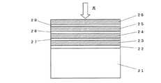
磁気旋光を利用する本発明のデバイスは低屈折率及び高屈折率の誘電体を交互に積層して、基板上に作製される誘電体多層膜と、この誘電体多層膜の上に設ける透明磁性層、さらに基板上の誘電体多層膜とまったく同一構成の誘電体多層膜を設ける。以上の透明磁性膜を挟んだ誘電体多層膜の一方の側に反射膜を設けて反射型ディスプレイが用いられる基本的な構成は図2に示す。
透明磁性体の厚みは可視光波長λの1/2n(n=磁性体の屈折率)に設定されるのでファラデー回転角が絶対的な大きさにおいて不十分な場合が生ずる。この場合は以上で述べた誘電体多層膜/透明磁性層/誘電体多層膜の構成をまったく同じにして複数回繰り返すことによって十分な(2回繰り返せば、約2倍)回転角を得ることができる。The device of the present invention using magnetic rotation is a dielectric multilayer film formed on a substrate by alternately laminating low-refractive index and high-refractive index dielectrics, and a transparent magnetic film provided on the dielectric multilayer film. A dielectric multilayer film having the same structure as that of the dielectric multilayer film on the substrate is further provided. FIG. 2 shows a basic configuration in which a reflective display is used by providing a reflective film on one side of a dielectric multilayer film sandwiching the above transparent magnetic film.
Since the thickness of the transparent magnetic material is set to 1 / 2n of the visible light wavelength λ (n = refractive index of the magnetic material), the Faraday rotation angle may be insufficient in absolute magnitude. In this case, it is possible to obtain a sufficient rotation angle by repeating the above-described dielectric multilayer film / transparent magnetic layer / dielectric multilayer film a plurality of times with exactly the same structure (about twice if repeated twice). it can.
偏光子を用いるのは上記誘電体多層膜/透明磁性層/誘電体多層膜/透明基板の構成において、透明磁性体の磁化された部位で得られた大きなファラデー回転角を画像として可視化するためである。すなわち透明磁性体の磁化された部位に対応して大きなファラデー回転角が得られ、磁化していない部位に対しては光の偏光面は回転しない。偏光面非回転部位では直線偏光はそのまま反射されて、もう一度上記誘電体多層膜/透明磁性層/誘電体多層膜を通過した後、偏光子も通過する。しかし偏光面回転部位を最初に通過した直線偏光は偏光面が透明磁性層で回転され反射膜で反射されて、もう一度上記透明磁性層を通過する際に回転して2倍の回転角を得るため、偏光子を通過できない。この原理によってコントラストを得ることができる。 The polarizer is used to visualize the large Faraday rotation angle obtained at the magnetized portion of the transparent magnetic material as an image in the above-mentioned configuration of the dielectric multilayer film / transparent magnetic layer / dielectric multilayer film / transparent substrate. is there. That is, a large Faraday rotation angle is obtained corresponding to the magnetized portion of the transparent magnetic material, and the polarization plane of light does not rotate with respect to the non-magnetized portion. The linearly polarized light is reflected as it is at the non-rotating portion of the polarization plane, passes through the dielectric multilayer film / transparent magnetic layer / dielectric multilayer film once again, and then passes through the polarizer. However, the linearly polarized light that first passes through the rotating part of the polarization plane is rotated by the transparent magnetic layer and reflected by the reflective film, and rotates again when passing through the transparent magnetic layer to obtain a double rotation angle. , Can not pass through the polarizer. Contrast can be obtained by this principle.
前記誘電体多層膜に用いられる材料としては前表1および2のものが挙げられる。これらの材料の中から適宜選択しても良いし、またこれ以外の例えば有機材料であってもかまわない。
前記多層膜の各膜厚は50〜200nm程度が好ましい。本発明のように特定波長(λ)の磁気光学効果増大を目的とする場合は、誘電体の膜厚は、λ/4n(nはλにおける誘電体の屈折率)とする。
また低屈折率及び高屈折率の誘電体を積層したものを1ペアとするとペア数には特に制限はないが、3〜20層が性能上またコスト上好ましい。透明磁性体と接する2つの誘電体多層膜はまったく同一の構成を有することが好ましい。ただし透明磁性体に直接に接する膜の種類は同じ誘電体を用いるので、積層順序は逆になる。
反射層としてはPVD法で設けられたAl、Cu、Ag、Au、Pt、Rh、Al2O3、SiO2、TeC、SeAs、TeAs、TiN、TaN、CrN等が用いられる。Examples of the material used for the dielectric multilayer film include those in Tables 1 and 2 above. These materials may be appropriately selected, and other materials such as organic materials may be used.
Each film thickness of the multilayer film is preferably about 50 to 200 nm. For the purpose of increasing the magneto-optical effect at a specific wavelength (λ) as in the present invention, the film thickness of the dielectric is λ / 4n (n is the refractive index of the dielectric at λ).
Further, when a pair of dielectrics having a low refractive index and a high refractive index is laminated, the number of pairs is not particularly limited, but 3 to 20 layers are preferable in view of performance and cost. The two dielectric multilayer films in contact with the transparent magnetic material preferably have exactly the same configuration. However, since the same dielectric is used as the type of film that is in direct contact with the transparent magnetic material, the stacking order is reversed.
As the reflective layer, Al, Cu, Ag, Au, Pt, Rh, Al2 O3 , SiO2 , TeC, SeAs, TeAs, TiN, TaN, CrN, and the like provided by the PVD method are used.
透明磁性層
透明磁性層としては従来一般に用いられている磁気光学効果を示す透明磁性材料で良いが、ファラデー効果が大きくて透明性の大きい所謂性能指数の大きい磁性材料が好ましい。例えば50nm以下の粒子径を有する、鉄、コバルト、Ni等の強磁性金属の超微粒子膜が用いられる。この場合の金属超微粒子以外の膜組成としては酸素、炭素などである。鉄、コバルト、Ni等の強磁性金属は大きな磁気光学効果を示すが、光の吸収も大きいためにそのままの薄膜では用いられなかったが、超微粒子膜とすると大きな性能指数を有するようになる。また粒子径の制御によって、適当な保磁力を得ることができる。ほかに希土類鉄ガーネットやコバルトフェライト、Baフェライト等の酸化物、FeBO3、FeF3、YFeO3、NdFeO3などの複屈折が大きな材料、MnBi、MnCuBi、PtCoなどがある。磁気光学効果は光の進行方向とスピンの方向とが平行の場合に最も大きな効果が得られるので、これらの材料は膜面に垂直に磁気異方性を有する膜が好ましい。これらの透明磁性材料は一般的なスパッタ真空蒸着、MBEなどのPVD法やCVD法、メッキ法等が用いられる。Transparent Magnetic Layer As the transparent magnetic layer, a transparent magnetic material exhibiting a magneto-optical effect that has been generally used may be used. However, a magnetic material having a large Faraday effect and high transparency, a so-called high performance index is preferable. For example, an ultrafine particle film of a ferromagnetic metal such as iron, cobalt, or Ni having a particle diameter of 50 nm or less is used. In this case, the film composition other than the ultrafine metal particles is oxygen, carbon or the like. Ferromagnetic metals such as iron, cobalt, and Ni show a large magneto-optical effect, but they are not used as they are because of their large light absorption. However, when they are made of ultrafine particles, they have a large figure of merit. Further, an appropriate coercive force can be obtained by controlling the particle diameter. In addition, there are oxides such as rare earth iron garnet, cobalt ferrite and Ba ferrite, materials with large birefringence such as FeBO3 , FeF3 , YFeO3 and NdFeO3 , MnBi, MnCuBi and PtCo. Since the magneto-optic effect is most effective when the light traveling direction and the spin direction are parallel, these materials are preferably films having magnetic anisotropy perpendicular to the film surface. For these transparent magnetic materials, general sputtering vacuum deposition, PVD method such as MBE, CVD method, plating method or the like is used.
(1)入射無偏光を非常に少ないロスでP偏光に変換して出射させ得ることが可能となった。
(2)変形が可能な偏光変換素子が得られた。
(3)直線状に狭く入射光をしぼることができ、全入射光の内のp波を非常に少ないロスで出射させ得ることが可能となった。
(4)出射光面に設けられた1/2波長板は液晶層で狭いストライプ状に、波長板機能と波長板機能を持たない部位が交互に一定のピッチで配列しているので、全入射光の内のS偏光を非常に少ないロスでP偏光に変換して、出射させ得ることが可能となった。
(5)素子への入射光の反射を防止でき、有効に光を利用できるので高いコントラストを得ることが可能になった。
(6)光の利用効率が向上して、高いコントラストの反射型ディスプレイが得られた。
(7)偏光変換素子と旋光性を利用して画像形成する反射型ディスプレイとを重ねて用いる場合に、旋光性材料を磁性ガーネット薄膜としたので、全体として格段に薄いディスプレイを得ることができる。(1) It has become possible to convert incident non-polarized light into P-polarized light with very little loss and emit it.
(2) A deformable polarization conversion element was obtained.
(3) The incident light can be narrowed linearly, and the p-wave of all the incident light can be emitted with very little loss.
(4) The half-wave plate provided on the outgoing light surface is a narrow stripe in the liquid crystal layer, and the portions that do not have the wave plate function and the wave plate function are alternately arranged at a constant pitch. It has become possible to convert S-polarized light in the light into P-polarized light with very little loss and to emit it.
(5) Reflection of incident light to the element can be prevented and light can be used effectively, so that high contrast can be obtained.
(6) The light utilization efficiency was improved, and a reflective display with high contrast was obtained.
(7) When a polarization conversion element and a reflective display that forms an image using optical rotation are used in an overlapping manner, since the optical rotatory material is a magnetic garnet thin film, an extremely thin display as a whole can be obtained.
以下に実施例によって詳しく説明する。
実施例1
偏光変換素子の構造および該素子の製造法
図1を用いて説明する。200μm厚(d)のポリカーボネート基板5の片面に、電子ビーム蒸着法を用いて、40μm厚(b)の五酸化タンタルで構成される複屈折率膜3を以下のようにして作製した。Ta2O5に金属Taを4重量%加えた粉末を蒸発源とした。前記ポリカーボネート基板5を150℃に加熱した。チャンバー内にはArと酸素の混合ガスを導入し、10−4Torrのガス圧力とした後、プラズマを発生させて製膜時には基板表面にイオンアシストできるようにした。また前記基板は蒸発源から真上に蒸発する粒子に対して、70度の傾斜を設けた。製膜速度は6nm/秒で数回にわけて製膜した。以上のようにして前記高複屈折膜3を作製した。該高複屈折膜3の断面をSEM観察すると、柱が基板面に対して70度程度傾斜した斜め配向柱状構造を有していた。膜の透過率は波長550nmの場合で75%であった。また、S偏光とP偏光のつくる角度(α)は約8.5度であった。Hereinafter, the present invention will be described in detail with reference to examples.
Example 1
The structure of the polarization conversion element and the manufacturing method of the element will be described with reference to FIG. A birefringence film 3 made of tantalum pentoxide having a thickness of 40 μm (b) was formed on one surface of a polycarbonate substrate 5 having a thickness of 200 μm (d) by using an electron beam evaporation method as follows. A powder obtained by adding 4% by weight of metal Ta to Ta2 O5 was used as an evaporation source. The polycarbonate substrate 5 was heated to 150 ° C. A mixed gas of Ar and oxygen was introduced into the chamber and a gas pressure of 10−4 Torr was generated, and then plasma was generated to enable ion assist on the substrate surface during film formation. The substrate was provided with an inclination of 70 degrees with respect to the particles evaporating directly from the evaporation source. The film formation speed was 6 nm / second and was formed several times. The high birefringence film 3 was produced as described above. When the cross section of the high birefringent film 3 was observed with an SEM, the column had an obliquely aligned columnar structure in which the column was inclined by about 70 degrees with respect to the substrate surface. The transmittance of the film was 75% at a wavelength of 550 nm. Further, the angle (α) formed between the S-polarized light and the P-polarized light was about 8.5 degrees.
前記高複屈折膜3の上に真空蒸着法を用いて100nm厚(a)のMgOの反射防止膜を設けた。高複屈折膜3の反射率は約3%低下した。
反射防止膜3の上には、レプリカ法で作製したポリカーボネート製マイクロレンズアレイ1を設けた。該マイクロレンズアレイ1の形状は、ストライプで、断面形状はかまぼこ型であり、そのピッチは12μm、焦点距離は1.1mmとした。
前記透明基板の高複屈折膜の反対面に、日産化学製のポリイミドSE7792をスピンコート法によって、60nmの厚み(c)に塗布した後、180℃で1時間ベークし乾燥させた。直線偏光された40mW/cm、2257nmの深紫外線をピッチP=12μm(照射部e=6μm、非照射部e′=6μm、P=2e)でストライプ状に押射した。深紫外線照射部では液晶配向が観察されて、配向容易軸方向は偏光方向に対して平行であった。その結果400〜800nmに対する偏光回転角は90度で、偏光変調子の機能を有する偏光変換素子が得られた。On the high birefringence film 3, an antireflection film of MgO having a thickness of 100 nm (a) was provided using a vacuum deposition method. The reflectance of the high birefringence film 3 was reduced by about 3%.
On the antireflection film 3, a
On a surface opposite to the high birefringence film of the transparent substrate, a polyimide SE7792 made by Nissan Chemical was applied by spin coating to a thickness (c) of 60 nm, and then baked at 180 ° C. for 1 hour and dried. Linearly polarized 40 mW / cm, 2257 nm deep ultraviolet rays were applied in a stripe shape with a pitch P = 12 μm (irradiation part e = 6 μm, non-irradiation part e ′ = 6 μm, P = 2e). Liquid crystal alignment was observed in the deep ultraviolet irradiation region, and the easy alignment axis direction was parallel to the polarization direction. As a result, the polarization rotation angle with respect to 400 to 800 nm was 90 degrees, and a polarization conversion element having the function of a polarization modulator was obtained.
磁気旋光を利用するディスプレイ
前記のようにして作製した偏光変換素子の液晶波長板の側に、次のようにして作製した磁気旋光を利用するディスプレイを設けた。
200μm厚のカーボン基板(日清紡製)21上に、真空蒸着法を用いて、アルミニウム(Al)の反射膜22を100nmの厚さに設けた。該反射膜22膜上にイオンプレーティング法を用いてSiO2(低屈折率層、n=1.47)を884nm、Ta2O5(高屈折率層、n=2.15)を605nmとして交互に4層づつ、合計8層積層し誘電体多層膜23を作製した。基板温度は300℃、酸素ガス圧力はSiO2の場合10×10−4Torr、Ta2O5の場合は11×10−4Torrであった。製膜速度は、SiO2の場合2nm/秒、Ta2O5の場合0.5nm/秒であった。各誘電体多層膜の膜厚分布は、最も厚いところと薄いところの差異が全膜厚の3%であった。Display using magnetic rotation The display using magnetic rotation produced as follows was provided on the liquid crystal wave plate side of the polarization conversion element produced as described above.
An aluminum (Al)
ついで、前記誘電体多層膜23の上にスパッタ法を用いてBi置換希土類鉄ガーネット膜(屈折率n=2.1)27を平均膜厚が520/2×2.1=124nmとなるように作製した。520nmは前記ガーネット膜の磁気旋光角度がピークを示す角度である。基板温度は400℃とした。ついでこの基板上の膜を空気中650℃で3時間加熱した。膜の組成はBi2.2Dy0.8Fe3.8Al1.2O12であった。磁気光学効果測定装置(日本分光株製K250、ビーム径2mm角)で測定したファラデー回転角の成長依存性からピークの半値幅を求めると18nmであった。波長520nmでは回転角のピーク値は2.0度であった。VSMで磁界を膜面に垂直に印加して測定した保磁力は600 Oeであった。Next, a Bi-substituted rare earth iron garnet film (refractive index n = 2.1) 27 is formed on the
ついでこのBi置換希土類鉄ガーネット膜上にイオンプレーティング法を用いて、前記とまったく同様に、SiO2とTa2O5の多層膜24を作製した。Bi置換希土類鉄ガーネット膜に接している膜はTa2O5であり、最表面側はSiO2である。ファラデー回転角の波長依存性から、波長520nmでは前記2.0の約6倍の12.0度の回転角であった。
前記誘電体多層膜24の上にもう2サイクル、前記と同様にしてBi置換希土類鉄ガーネット膜を2回と誘電体多層膜4ペアを2回設けた。ガーネット膜は合計3層、4ペアの誘電体多層膜は合計4×4ペア、すなわち16ペア、32層設けたことになる。波長520nmでは前記ガーネット1層の場合の2.0の約12倍の24.0度の回転角であった。
前記の磁気旋光利用ディスプレイを前記偏光変換素子の液晶波長板の側に基板を下にして配設した。この場合ディスプレイの非磁化部位に入射して反射膜で反射した戻り光の比率は、入射光強度に対して約36%(波長550nm)であった。Then, a
Two cycles of Bi-substituted rare earth iron garnet film and two pairs of dielectric multilayer films were provided twice on the
The display using magnetic rotation was disposed on the liquid crystal wave plate side of the polarization conversion element with the substrate facing down. In this case, the ratio of the return light incident on the non-magnetized portion of the display and reflected by the reflective film was about 36% (wavelength 550 nm) with respect to the incident light intensity.
前記の磁気旋光利用ディスプレイの最表面の誘電体多層膜上から永久磁石(表面磁束密度3Kガウス)のついた磁気ペンで文字を書いた。磁気ペンで磁化した部位では前記偏光変換素子を通過して入射した直線偏光の偏光面が回転して、もとの偏光変換素子へ戻ることなく、従って磁気ペンで書いた文字が黒く表示された。画像部分のコントラストは6.5であった。 Characters were written with a magnetic pen with a permanent magnet (surface magnetic flux density 3K gauss) on the outermost dielectric multilayer film of the display using magnetic rotation. In the part magnetized with the magnetic pen, the plane of polarization of the linearly polarized light that has passed through the polarization conversion element rotates and does not return to the original polarization conversion element, so the characters written with the magnetic pen are displayed in black. . The contrast of the image portion was 6.5.
実施例2
実施例1の前記偏光変換素子の透過率は波長550nmの場合で70%であったのに対し、実施例1において、市販のヨウ素を用いた吸収タイプのフィルム偏光子を用いた場合には、得られた偏光変換素子透過率は波長550nmの場合で43%であった。Example 2
While the transmittance of the polarization conversion element of Example 1 was 70% at a wavelength of 550 nm, in Example 1, when an absorption type film polarizer using commercially available iodine was used, The transmittance of the obtained polarization conversion element was 43% when the wavelength was 550 nm.
実施例3
実施例1の偏光変換素子の作製において用いた、透明基板およびマイクロレンズアレイとしてのポリカーボネートをいずれもガラスとした以外は実施例1とまったく同様にして偏光変換素子を作製した。実施例1の偏光変換素子は落したり、また多少の曲げに対しても破損することはなかったが、ガラスを用いた本実施例のものは、実施例1のものに比較して破損し易かった。Example 3
A polarization conversion element was produced in exactly the same manner as in Example 1 except that the transparent substrate and the polycarbonate as the microlens array used in the production of the polarization conversion element of Example 1 were both made of glass. Although the polarization conversion element of Example 1 was not dropped or damaged by some bending, the example of this example using glass was more easily damaged than that of Example 1. It was.
実施例4
実施例1のかまぼこ型マイクロレンズアレイの代わりに、上から見た場合の形状が4角形であるマイクロレンズアレイとした以外は実施例1とまったく同様にして偏光変換素子を作製した。2mm角の光照射面積で測定した光強度(波長550nm)は実施例1に対して66%と滅少した。Example 4
Instead of the kamaboko type microlens array of Example 1, a polarization conversion element was produced in exactly the same manner as in Example 1 except that a microlens array having a quadrangular shape when viewed from above was used. The light intensity (wavelength 550 nm) measured with a light irradiation area of 2 mm square decreased to 66% compared to Example 1.
実施例5
市販のフィルム波長板を細線状にカットして、実施例1で作製した偏光変換素子のように、基板の出射側に貼付しようとしたが、1mm以下の幅では直線状に並べることはできなかった。Example 5
A commercially available film wave plate was cut into a thin line shape and tried to be attached to the output side of the substrate like the polarization conversion element produced in Example 1, but it could not be arranged linearly with a width of 1 mm or less. It was.
実施例6
実施例1で作製した磁気旋光利用ディスプレイを、市販のフィルム偏光子の下に配置した。この場合ディスプレイの非磁化部位に入射して、反射膜で反射した戻り光の比率は、入射光強度に対して約11%(波長550nm)と実施例1に比較して、1/3と低かった。フィルム偏光子の上から永久磁石のついた磁気ペンで一部を磁化した。磁気ペンで磁化した部位では、上記偏光子を通過して入射した直線偏光の偏光面が回転して、もとの偏光子へ戻ることなく、従って磁気ペンで書いた文字が黒く表示された。画像部分のコントラストは2.3であった。Example 6
The display using magnetic rotation prepared in Example 1 was placed under a commercially available film polarizer. In this case, the ratio of the return light incident on the non-magnetized portion of the display and reflected by the reflecting film is about 11% (wavelength 550 nm) with respect to the incident light intensity, which is 1/3 lower than that of Example 1. It was. Part of the film was magnetized with a magnetic pen with a permanent magnet from above the film polarizer. In the part magnetized with the magnetic pen, the plane of polarization of the linearly polarized light that passed through the polarizer was rotated and did not return to the original polarizer. Therefore, the characters written with the magnetic pen were displayed in black. The contrast of the image portion was 2.3.
実施例7
実施例1で作製した磁気旋光利用ディスプレイの磁性材料としてBaフェライト薄膜を用いた以外は、実施例1と同様にして偏光変換素子と併せたディスプレイを作製した。波長520nmでは、偏光面回転角のピーク値は8.6度であった。VSMで磁界を膜面に垂直に印加して測定した保磁力は、9600 Oeであった。最表面の誘電体多層膜上から永久磁石のついた磁気ペンで文字を書いた。磁気ペンで磁化した部位では書いた文字が黒く表示された。画像部分のコントラストは2.5であった。Example 7
A display combined with a polarization conversion element was produced in the same manner as in Example 1 except that a Ba ferrite thin film was used as the magnetic material of the display using magnetic rotation prepared in Example 1. At a wavelength of 520 nm, the peak value of the polarization plane rotation angle was 8.6 degrees. The coercive force measured by applying a magnetic field perpendicularly to the film surface with VSM was 9600 Oe. Letters were written with a magnetic pen with permanent magnets on the outermost dielectric multilayer film. The written characters were displayed in black at the part magnetized with the magnetic pen. The contrast of the image portion was 2.5.
1 マイクロレンズアレイ
2 反射防止膜
3 複屈折性を有する薄膜
4 液晶波長板
5 可視光に透明な基板
6 自然光
21 基板
22 反射層
23 誘電体多層膜(4ペア)
24 誘電体多層膜(4ペア)
25 誘電体多層膜(4ペア)
26 誘電体多層膜(4ペア)
27 磁性層
28 磁性層
29 磁性層
a 反射防止膜の厚さ
b 複屈折性を有する薄膜の厚さ
c 液晶波長板の厚さ
d 透明な基板の厚さ
e 波長板機能を持たない部位の幅
e′ 波長板機能を持つ部位の幅
DESCRIPTION OF
24 Dielectric multilayer (4 pairs)
25 Dielectric multilayer (4 pairs)
26 Dielectric multilayer (4 pairs)
27
Claims (2)
Translated fromJapanesePriority Applications (1)
| Application Number | Priority Date | Filing Date | Title |
|---|---|---|---|
| JP2006049870AJP4203507B2 (en) | 2006-02-27 | 2006-02-27 | Polarization conversion element and display device using the polarization conversion element |
Applications Claiming Priority (1)
| Application Number | Priority Date | Filing Date | Title |
|---|---|---|---|
| JP2006049870AJP4203507B2 (en) | 2006-02-27 | 2006-02-27 | Polarization conversion element and display device using the polarization conversion element |
Related Parent Applications (1)
| Application Number | Title | Priority Date | Filing Date |
|---|---|---|---|
| JP22543698ADivisionJP3971035B2 (en) | 1998-07-24 | 1998-07-24 | Polarization conversion element and display device using the polarization conversion element |
Publications (2)
| Publication Number | Publication Date |
|---|---|
| JP2006171791A JP2006171791A (en) | 2006-06-29 |
| JP4203507B2true JP4203507B2 (en) | 2009-01-07 |
Family
ID=36672512
Family Applications (1)
| Application Number | Title | Priority Date | Filing Date |
|---|---|---|---|
| JP2006049870AExpired - Fee RelatedJP4203507B2 (en) | 2006-02-27 | 2006-02-27 | Polarization conversion element and display device using the polarization conversion element |
Country Status (1)
| Country | Link |
|---|---|
| JP (1) | JP4203507B2 (en) |
- 2006
- 2006-02-27JPJP2006049870Apatent/JP4203507B2/ennot_activeExpired - Fee Related
Also Published As
| Publication number | Publication date |
|---|---|
| JP2006171791A (en) | 2006-06-29 |
Similar Documents
| Publication | Publication Date | Title |
|---|---|---|
| JP3654553B2 (en) | Optical element | |
| US7453640B2 (en) | Liquid crystal display including O-type and E-type polarizer | |
| US8068387B2 (en) | Magneto-optical device | |
| CN106133566B (en) | Optical device with patterned anisotropy incorporating parallax optics | |
| CN1282896C (en) | Liquid crystal display containing O-type and E-type polarizers | |
| JP4785790B2 (en) | Polarization conversion element | |
| JP5001807B2 (en) | Spatial light modulator | |
| JP3971035B2 (en) | Polarization conversion element and display device using the polarization conversion element | |
| JP2003066232A (en) | Multilayer diffractive polarizer and composite liquid crystal device | |
| JP3753853B2 (en) | Magneto-optical element and magneto-optical device | |
| JPH10332932A (en) | Filter that polarizes light in a specific wavelength range | |
| JP4203507B2 (en) | Polarization conversion element and display device using the polarization conversion element | |
| JP3781553B2 (en) | Light shutter | |
| JP2006301657A (en) | Polarized light transforming element and display device | |
| JPH10213785A (en) | Polarizer, method of manufacturing the same, and display or display device including the polarizer | |
| JP3626576B2 (en) | Magneto-optic element | |
| JP2000171633A (en) | Polarization conversion element and display device using the polarization conversion element | |
| JP3850387B2 (en) | Method for producing polarizer and polarizer | |
| JP4033368B2 (en) | Magnetic display medium | |
| JP2000162549A (en) | Polarization conversion element, display device using the same, and projection display device | |
| JP2000267057A (en) | Magneto-optical element | |
| JP3560431B2 (en) | Display device | |
| JP3754557B2 (en) | Magneto-optic element | |
| JP3771023B2 (en) | Magneto-optical element for display | |
| JPH11176637A (en) | Polarizer and magneto-optical element |
Legal Events
| Date | Code | Title | Description |
|---|---|---|---|
| A131 | Notification of reasons for refusal | Free format text:JAPANESE INTERMEDIATE CODE: A131 Effective date:20080415 | |
| A521 | Written amendment | Free format text:JAPANESE INTERMEDIATE CODE: A523 Effective date:20080616 | |
| A131 | Notification of reasons for refusal | Free format text:JAPANESE INTERMEDIATE CODE: A131 Effective date:20080715 | |
| A521 | Written amendment | Free format text:JAPANESE INTERMEDIATE CODE: A523 Effective date:20080901 | |
| TRDD | Decision of grant or rejection written | ||
| A01 | Written decision to grant a patent or to grant a registration (utility model) | Free format text:JAPANESE INTERMEDIATE CODE: A01 Effective date:20081007 | |
| A01 | Written decision to grant a patent or to grant a registration (utility model) | Free format text:JAPANESE INTERMEDIATE CODE: A01 | |
| A61 | First payment of annual fees (during grant procedure) | Free format text:JAPANESE INTERMEDIATE CODE: A61 Effective date:20081010 | |
| R150 | Certificate of patent or registration of utility model | Free format text:JAPANESE INTERMEDIATE CODE: R150 | |
| FPAY | Renewal fee payment (event date is renewal date of database) | Free format text:PAYMENT UNTIL: 20111017 Year of fee payment:3 | |
| FPAY | Renewal fee payment (event date is renewal date of database) | Free format text:PAYMENT UNTIL: 20121017 Year of fee payment:4 | |
| FPAY | Renewal fee payment (event date is renewal date of database) | Free format text:PAYMENT UNTIL: 20131017 Year of fee payment:5 | |
| LAPS | Cancellation because of no payment of annual fees |