JP4200951B2 - Contactless data carrier, its terminal equipment and access system - Google Patents
Contactless data carrier, its terminal equipment and access systemDownload PDFInfo
- Publication number
- JP4200951B2 JP4200951B2JP2004218746AJP2004218746AJP4200951B2JP 4200951 B2JP4200951 B2JP 4200951B2JP 2004218746 AJP2004218746 AJP 2004218746AJP 2004218746 AJP2004218746 AJP 2004218746AJP 4200951 B2JP4200951 B2JP 4200951B2
- Authority
- JP
- Japan
- Prior art keywords
- information
- data carrier
- read
- reading
- terminal device
- Prior art date
- Legal status (The legal status is an assumption and is not a legal conclusion. Google has not performed a legal analysis and makes no representation as to the accuracy of the status listed.)
- Expired - Fee Related
Links
- 238000004891communicationMethods0.000claimsdescription44
- 238000012790confirmationMethods0.000claimsdescription33
- 230000003287optical effectEffects0.000claimsdescription32
- 238000000034methodMethods0.000claimsdescription9
- 239000000969carrierSubstances0.000claimsdescription7
- 230000005540biological transmissionEffects0.000description15
- 238000001444catalytic combustion detectionMethods0.000description12
- 238000012545processingMethods0.000description9
- 239000004973liquid crystal related substanceSubstances0.000description8
- 238000005286illuminationMethods0.000description7
- 239000003550markerSubstances0.000description6
- 239000003990capacitorSubstances0.000description4
- 238000006243chemical reactionMethods0.000description4
- 238000009499grossingMethods0.000description4
- 238000003384imaging methodMethods0.000description4
- 230000004044responseEffects0.000description3
- 238000010586diagramMethods0.000description2
- 230000006870functionEffects0.000description2
- 230000003321amplificationEffects0.000description1
- 230000000694effectsEffects0.000description1
- 239000000284extractSubstances0.000description1
- 238000010030laminatingMethods0.000description1
- 238000012986modificationMethods0.000description1
- 230000004048modificationEffects0.000description1
- 238000003199nucleic acid amplification methodMethods0.000description1
- 239000004065semiconductorSubstances0.000description1
- 238000012795verificationMethods0.000description1
Images


Landscapes
- Credit Cards Or The Like (AREA)
Description
Translated fromJapanese本発明は非接触型データキャリア、その端末機器およびアクセスシステムに係り、特に端末機器がデータを読み取りおよび/または書込みの対象とするデータキャリアを間違えないようにすることができるようにしたものに関する。 The present invention relates to a contactless data carrier, a terminal device thereof, and an access system, and more particularly, to a terminal device capable of preventing a data carrier from which data is read and / or written from being mistaken.
最近、磁気カードに比べて記憶容量の大きな非接触型のICカード(データキャリア)が各種用途の情報記録媒体として採用されてきている。この非接触型のICカードは、リーダライタ(端末機器)より送信される特定周波数の電波から電力を取得してリーダライタとの間でデータを送受するように構成されている(例えば、特許文献1)。
非接触式のICカードは電波によりリーダライタと通信する構成であるため、リーダライタから発せられる電波の受信範囲内にデータを送受しようとするICカードとは別のICカードが存在していた場合、リーダライタは別のICカードと通信(通信相手の誤認)してしまうことがある。
このような通信相手の誤認は厳に避けなければならない。特に、ICカードが電子マネーの決済用として使用されていた場合、通信相手の誤認を生ずると、使用者の知らないうちに、電子マネーの残高が減らされているという重大な問題を生ずる。Since the non-contact type IC card is configured to communicate with the reader / writer by radio waves, there is an IC card that is different from the IC card to be transmitted / received within the reception range of the radio waves emitted from the reader / writer. The reader / writer may communicate with another IC card (misidentification of the communication partner).
Such misidentification of the communication partner must be strictly avoided. In particular, when an IC card is used for settlement of electronic money, if a communication partner is misidentified, a serious problem occurs that the balance of electronic money is reduced without the user's knowledge.
本発明は上記の事情に鑑みてなされたもので、その目的は、リーダライタが通信相手の誤認を生ずることなく、正規のデータキャリアと通信することができる非接触型データキャリア、その端末機器およびアクセスシステムを提供することにある。The present invention has been made in view of the above circumstances, and an object of the present invention is to provide a non-contact data carrier capable of communicating with a legitimate data carrier without causing a reader / writer to misidentify a communication partner, itsterminal device, and To provide an access system.
上記の目的を達成するために、本発明では、非接触型データキャリアは、端末機器と通信する通信手段の他に、事前確認情報を記憶したメモリ、事前確認情報と一致する情報を光学的に読み取り可能な形態で表示した光学的情報表示部を有する。一方、端末機器は、データキャリアの前記通信手段と非接触で通信する通信手段、データキャリアの光学的情報表示部を光学的に読み取る光学的情報読取手段を有する。 In order to achieve the above object, according to the present invention, the contactless data carrier optically transmits information that matches the prior confirmation information in addition to the communication means that communicates with the terminal device. It has an optical information display unit displayed in a readable form. On the other hand, the terminal device has communication means for communicating in a non-contact manner with the communication means of the data carrier, and optical information reading means for optically reading the optical information display section of the data carrier.
請求項1、2、3の発明では、端末機器が、まず通信可能な全てのデータキャリアから事前確認情報および書き換え可能な情報を読み取り、その後に光学的表示部から事前確認情報を読み取って、先に通信手段にて読み取ったデータキャリアの中に、光学的表示部から読み取った事前確認情報事に一致するデータキャリアがあったとき、そのデータキャリアから読み取った書き換え可能な情報、つまり読み取りおよび/または書込みのために必要な情報を選択処理するので、読み取りおよび/または書込みのための処理時間を短縮することができる。なお、このように通信可能な全てのデータキャリアから事前確認情報および書き換え可能な情報を読み取る方式は、端末機器の記憶容量との関係で、データキャリアの情報量が比較的少ない場合に適する。In the inventionof claim1, 2, the terminal device reads the pre-verification information and the rewritable information from first communicable all data carriers, and then reads the pre-confirmation information from the optical display unit, the previously When there is a data carrier that matches the prior confirmation information read from the optical display unit in the data carrier read by the communication means, rewritable information read from the data carrier, that is, read and / or Since information necessary for writing is selectively processed, processing time for reading and / or writing can be shortened. The method of reading the prior confirmation information and the rewritable information from all communicable data carriers in this way is suitable when the information amount of the data carrier is relatively small in relation to the storage capacity of the terminal device.
請求項4、5の発明では、端末機器が通信手段により事前確認情報を読み取ったデータキャリアが1つしかないとき、光学的情報読取手段による読み取りを行うことなく、次の動作に進むので、読み取りおよび/または書込みのための処理時間を短縮することができる。
請求項6、7の発明では、トリガースイッチを操作しないと、通信手段、光学的情報読取手段による事前確認情報の読み取りを行わないので、端末機器の消費電力を極力抑えることができる。According to the fourth andfifth aspects of the present invention, when there is only one data carrier from which the terminal device has read the prior confirmation information by the communication means, the process proceeds to the next operation without performing the reading by the optical information reading means. And / or processing time for writing can be reduced.
According to thesixth and seventh aspects of the present invention, if the trigger switch is not operated, the prior confirmation information is not read by the communication means and the optical information reading means, so that the power consumption of the terminal device can be suppressed as much as possible.
[第1の参考例]
以下、本発明の第1の参考例を図1ないし図5に基づいて説明する。
図4はデータキャリアとしてのICカード1を示すもので、このICカード1は複数枚のプラスチック薄板を積層して構成され、その表面には、情報コード(光学的情報表示部)として二次元コードの一種であるQRコード2が印刷により設けられている。QRコード1はラベルに印刷したものをICカード1に貼り付けるものであっても良い。このICカード1と電波により通信してコマンド、データを送受する端末機器としてのリーダライタ3は図2に示されている。このリーダライタ3は、本実施例では携帯型として構成され、QRコード2の画像を取り込んで解読する機能と、ICカード1と電波により通信してデータの読み書きを行う機能とを有している。[FirstReference Example]
Hereinafter, a first exemplary embodiment ofthe present inventionyou described with reference to FIGS. 1 to5.
FIG. 4 shows an IC card 1 as a data carrier. This IC card 1 is formed by laminating a plurality of plastic thin plates, and a two-dimensional code is provided on the surface as an information code (optical information display unit). QR code 2 is provided by printing. The QR code 1 may be a label printed on a label and affixed to the IC card 1. A reader /
上記リーダライタ3は、手持ち可能なケース4を主体とするもので、そのケース4には、握り部を構成する操作部5、液晶表示器6などが設けられている。操作部5には、多数のキースイッチ7が設けられ、これらキースイッチ7によって動作内容などを指示するようになっている。リーダライタ3のケース4内には、プリント配線基板8が設けられており、このプリント配線基板8の一方の面に前記液晶表示器6およびキースイッチ群7が配設され、他方の面に光学的読取手段としてCCDエリアセンサ9および結像レンズ10が配設されている。 The reader /
ケース4の前端開口は読取口4aとされ、ここに別のプリント配線基板11が設けられている。このプリント配線基板11の前面側には、中央に形成された孔11aの周囲に位置して照明用光源としてのLED(発光ダイオード)12が搭載されていると共に、このLED12に対向する照明用レンズ13が配設されている。また、ケース4内において、読取口4aと結像レンズ10との間には、反射ミラー14が配設されている。 The front end opening of the
QRコード2の読み取りは、読取口4aをICカード1にほぼ接触させた状態で行う。そして、LED12の発する光は照明用レンズ13により拡散されてICカード1を照明し、その反射光は読取口4aから入射され、途中で反射ミラー14により曲げられて結像レンズ10によってCCDエリアセンサ9に結像されるようになっている。
一方、読取口4aのプリント配線基板11の表裏両側にはボビン15および16が設けられており、表側のボビン15に送信アンテナコイル17が巻装され、裏側のボビン16に受信アンテナコイル18が巻装されている。なお、送信アンテナコイル17および受信アンテナコイル18は、1個のアンテナコイルで共用する構成であっても良い。The QR code 2 is read in a state where the
On the other hand,
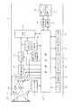
図1はリーダライタ3の電気的構成を示しており、上述した液晶表示器6、キースイッチ群7、CCDエリアセンサ9、LED12、通信手段としての送信アンテナコイル17、同じく通信手段としての受信アンテナコイル18の他に、制御手段としての制御回路19、増幅回路20、A/D変換回路21、同期パルス発生回路22、アドレス発生回路23、画像メモリ24、通信I/F回路25、復調部26、変調部27などを備えている。
制御回路19は、CPU、ROM、RAM、I/Oなどを備えたマイクロコンピュータタシステムとして構成され、ROMに記憶されているプログラムに従って動作する。また、制御回路19には、液晶表示器6、キースイッチ群7、通信I/F回路25などが接続されている。FIG. 1 shows the electrical configuration of the reader /
The
CCDエリアセンサ9は受光素子であるCCDを二次元的に配列して有し、LED12の反射光を結像してその二次元画像を水平方向の走査線信号として増幅回路20に与えられる。増幅回路20は、制御回路19からのゲインコントロール電圧に対応する増幅率でCCDエリアセンサ9から出力された走査線信号を増幅し、A/D変換回路21に出力する。そして、A/D変換回路21は、アナログの走査線信号をデジタル信号に変換する。このA/D変換回路21でデジタル信号に変換されたデータは多値データであり、この多値データは画像メモリ24に記憶される。そして、制御回路19が画像メモリ24に記憶された多値データに基づいて二次元コードを解読し、一時記憶手段としてのRAMに記憶させる。なお、この多値データは、各画素が8ビット(0〜255)の階調値を有するものとなっている。 The
同期パルス発生回路22は、CCDエリアセンサ9から出力される二次元画像データのパルスより十分細かい同期パルスを出力する。アドレス発生回路23は、この同期パルス発生回路22から与えられる同期パルスをカウントして画像メモリ24に対するアドレスを発生させる。そして、デジタル信号に変換された多値の画像データはアドレス毎に8ビット単位で画像メモリ24に書き込まれる。なお、液晶表示器6は例えば2階調の液晶として構成されており、画像メモリ24に書き込まれた画像データを表示するためなどに用いられる。 The synchronization
通信I/F回路25は、ホストコンピュータなどの外部装置との間で通信を行うものであり、例えば図示しない通信用発光素子を介して外部装置に送信したり、図示しない通信用受光素子を介して外部装置からの信号を受信したりする。
送信アンテナコイル17、受信アンテナコイル18、復調部26、変調部27は、ICカード1と通信を行うためのもので、変調部27はICカード1との通信時に、まず基準信号を変調して電力用電波信号として送信アンテナコイル17から送信し、その後、送信すべきデータを電力用電波信号に重畳して送信アンテナコイル17から送信する。また、復調部26は、受信アンテナコイル18により受信した電波信号を復調し、データとして取り出す。The communication I /
The transmitting
一方、ICカード1は、図3に示すように、電波信号を送受信するための通信手段としてのアンテナコイル28と、共振コンデンサ29と、制御用IC30と、平滑部31とを備えている。これらアンテナコイル28、共振コンデンサ29、制御用IC30、平滑部31は、ICカード1を構成する複数枚のプラスチック薄板の間に介装されている(図4には、アンテナコイル28と制御用IC30のみ図示した。)。 On the other hand, as shown in FIG. 3, the IC card 1 includes an
制御用IC30は、制御手段としてのCPU32の他、整流部33、変復調部34、識別情報および管理情報などのメモリ手段としてのメモリ部35などを構成する半導体素子をワンチップ化したものである。この場合、メモリ部35は、動作プログラムなどを記憶したROM36と、一時記憶用として消去可能な不揮発性メモリ、例えばEEPROM37とを有している。 The
メモリであるEEPROM37には、事前確認情報としての例えばパスワードが記憶されている。このEEPROM37に記憶されたパスワードは、前述したICカード1の表面に付されたQRコード2中にもQRコード化されて表示されている。なお、共振コンデンサ29は、制御用IC30に設けても良いし、場合によってはなくとも良い。
上記アンテナコイル28は、共振コンデンサ29と並列に接続されて共振回路を構成し、リーダライタ3の送信アンテナコイル17から所定の高周波数の電力用電波信号が送信されてくると、これを受信して整流部33に供給する。整流部33は、平滑部31と共に動作用電源回路を構成するもので、共振回路から送信されてきた電力用電波信号を整流し、平滑部31により平滑化し且つ一定電圧の直流電力(動作用電力)にしてCPU32などに供給する。The
The
電力用電波信号に重畳して送信されるコマンド信号やデータ信号は、変復調部34により復調されてCPU32に与えられる。CPU32は、メモリ部35のROM36に記憶された動作プログラムに従って動作するもので、変復調部34から入力される信号に応じた処理を実行し、受信したデータをメモリ部35のEEPROM37などに書き込んだり、EEPROM37からデータを読み出して変復調部34により変調し、アンテナコイル28から電波信号として送信したりする。 The command signal and data signal transmitted by being superimposed on the power radio signal are demodulated by the
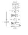
次にリーダライタ3がICカード1と通信する場合の作用を図5のフローチャートをも参照しながら説明する。
ICカード1の上にリーダライタ3の読取口4aを宛がい、この状態でキースイッチ群7の中から所定のキースイッチを操作してスタートさせる。すると、制御回路19は、まず、LED12を点灯させてQRコード2部分を照明する。これにより、その反射光が結像レンズ10によってCCDエリアセンサ9に結像される。このCCDエリアセンサ9に結像されたQRコード2の画像は多値のデジタルデータとして画像メモリ24に取り込まれる。そして、制御回路19は、画像メモリ24に取り込まれたQRコード2の画像をコード解読プログラムに従って解読する(以上、ステップS1;解読手段)。この場合、QRコード2はICカード1のパスワードを表しているので、制御回路19はQRコート2の解読によってICカード1のパスワードを取得する。Next, the operation when the reader /
The reading
次に、制御回路19は、送信アンテナコイル17から電力用電波信号を送信してICカード1と通信し、パスワード読み取りコマンドを送信する。すると、ICカード1のCPU32はEEPROM37からパスワードを読み取り、これをアンテナコイル28から電波信号として送信する。このICカード1から送信された電波信号はリーダライタ3の受信アンテナコイル18により受信され、復調部26により復調されて制御回路19に与えられる。これにより、リーダライタ3の制御回路19はICカード1から電波信号によってパスワードを取得する(以上、ステップS2)。 Next, the
このようにしてICカード1のQRコード2とEEPROM37との双方から情報を取得すると、次に制御回路19は取得した2つの情報を比較し、一致しているか否かを判断する(ステップS3;判断手段)。そして、2つの情報が一致していなかった場合(ステップS3で「NO」)、制御回路19は、電波による通信で取得したパスワードは、読み書きの対象としているICカードではなく、リーダライタ3から送信される電波の受信範囲内にある別のICカードから取得したものとして警報処理、例えば液晶表示器6にその旨を文字などによって表示する(ステップS5)。なお、警報処理としては、ブザーを鳴動させるものであっても良い。 When information is acquired from both the QR code 2 of the IC card 1 and the
2つの情報が一致していた場合(ステップS3で「YES」)、制御回路19は、電波による通信で取得したパスワードは、読み書きの対象としているICカードのものである、つまりCCDエリアセンサ10から読み込んだQRコード2を有するICカード2のものであるとして読み書き処理(EEPROM37の記憶データを読み出したり、EEPROM37にデータを書き込んだりする処理)を実行する(ステップS4)。この場合の読み書き処理は、ICカード2が電子マネーのICカードであれば、EEPROM37に記憶されている残高を読み出し、その残高から今回の取引額を差し引いて決済し、決済後の額を新たな残高としてICカード1に送信してEEPROM37の記憶する残高を書き換えるというものである。 When the two pieces of information match (“YES” in step S3), the
このように本参考例によれば、リーダライタ3は読取口4aが宛がわれたICカード1のQRコード2から情報を取得し、この情報が電波による通信によりEEPROM37から取得した事前確認情報と一致するか否かを判断し、一致しているときにだけ読み書き処理を実行するので、読み書きすべきICカード2とは別のICカードに対して読み書きしてしまう恐れがない。このため、電子マネーのICカードとして利用した場合、使用者の知らないうちに残高が減らされているといった不具合を生ずる恐れがない。As described above, according to thisreference example, the reader /
[第2の参考例]
図6は本発明の第2の参考例を示す。ICカードおよびリーダライタの構成は上述の第1の参考例と同様であるので、上述の第1の参考例で使用した名称および符号を使用して図6を参照しながら説明する。
ICカード1の上にリーダライタ3の読取口4aを宛がい、この状態でキースイッチ群7の中から所定のキースイッチを操作してスタートさせる。すると、制御回路19は、前述の一実施例の場合と同様にして、QRコード2を取り込み(ステップA1)、ICカード1のパスワードを取得する(ステップA2)。[SecondReference Example]
FIG. 6 shows a secondreference example of the present invention. The configuration of the IC card and the reader-writer isthe same asin thefirst reference example described above,it described with reference to FIG. 6 using the names and codes used inthe first reference example describedabove.
The reading
次に、制御回路19は、送信アンテナコイル17から電力用電波信号を送信してICカード1と通信し、解読したパスワードを送信する(ステップA3)。すると、ICカード1のCPU32は、EEPROM37からパスワードを読み取り、これをリーダライタ3から送信されてきた情報と比較し、両者が一致しているか否かを判断する(ステップA4;判断手段)。 Next, the
そして、CPU32は、EEPROM37から読み取ったパスワードとリーダライタ3から送信されてきた情報とが一致していなかった場合(ステップA4で「NO」)、アクセス不許可の信号をアンテナコイル28から送信する(ステップA6)。また、両者が一致していた場合(ステップA4で「YES」)、CPU32は、アクセス許可の信号をアンテナコイル28から送信する(ステップA5)。 If the password read from the
このICカード1から送信された信号はリーダライタ3によって受信される。そして、制御回路19は、受信した信号がアクセス許可の信号であるか否かを判断し(ステップA7)、アクセス不許可の信号であった場合(ステップA7で「NO」)、警報処理、例えば液晶表示器6にその旨を文字などによって表示する(ステップA9)。受信した信号がアクセス許可の信号であった場合、制御回路19は、読み書き処理を実行する(ステップS4)。 A signal transmitted from the IC card 1 is received by the reader /
このように本参考例によれば、ICカード1はリーダライタ3から送信された情報が自身のパスワードであった場合、つまりリーダライタ3が宛がわれてQRコード2を読み取られたICカードである場合、アクセス許可を送信するが、リーダライタ3から送信された情報が自身のパスワードでなかった場合には、リーダライタ3が宛がわれてQRコード2を読み取られたICカードではないから、アクセス不許可を送信する。このため、リーダライタ3が読み書きをするべきICカード以外のICカードと通信する恐れがない。
なお、ICカード1からのアクセス許可信号の送信は省略することができる。この場合には、バスワードと共に、読み書きのためのコマンドをICカード1に送信するので、他のICカード1がリーダライタ3からのコマンドを実行する恐れはない。Thus, according to thisreference example, the IC card 1 is an IC card in which the information transmitted from the reader /
The transmission permission signal from the IC card 1 isRu may beomitted. In this case, since the command for reading and writing is transmitted to the IC card 1 together with the password, there is no fear that another IC card 1 executes the command from the reader /
[第3の実施例]
図7および図8は、本発明の第3の参考例を示す。[Third embodiment]
7 and 8 show a thirdreference example of the present invention.
この参考例は、データキャリアをICカードではなく、RFIDタグ38(図7参照)としたもので、その電気的構成は図3と同一である。また、RFIDタグ38には、QRコード2(図示はないが、先の参考例と同一の符号を使用する。)が設けられている。このQRコード2には、事前確認情報として識別(ID)情報が表示されている他、コマンドおよびコマンドに関する情報が表示されている。コマンドおよびコマンドに関する情報とは、この実施例では、読み取りコマンドと書込みコマンド、書込みコマンドに関する情報として、その書込みは端末機器3から送信される現在時刻を書き込むという情報である。In thisreference example , the data carrier is not an IC card but an RFID tag 38 (see FIG. 7), and its electrical configuration is the same as FIG. The
端末機器3の電気的構成は、図7に示すように、基本的には図1と同様で、異なるところは、キースイッチからなるトリガースイッチ39、マーカー用LED40、ブザー41、表示用の緑色LED42、赤色LED43および時計部44を設けたところが相違する。トリガースイッチ39は、二段押し込み型のもので、一段押しすると、マーカー用LED40が点灯し、二段押しすると、照明用LED12が点灯するようになっている。 As shown in FIG. 7, the electrical configuration of the
本参考例は、図8のフローチャートに示すように、端末機器3が読み取ったQRコード2の識別情報をRFIDタグ38に送信する際に、併せてQRコード2から読み取ったコマンドを併せて送信するようにしたことを特徴としている。即ち、端末機器3の読取口4aを、読み取り対象となっているRFIDタグ38のQRコード2に宛て、そしてトリガースイッチ39を一段押しする(ステップB1)。すると、端末装置3の制御回路19は、マーカー用LED40を点灯(ステップB2)させて読み取り範囲を表示するので、QRコード2が読み取り範囲内にあることを確認した上で、トリガースイッチ39をもう一段押し込む(二段目押し込み)。これにより、照明用のLED12が点灯してQRコード2部分を照明すると共に、CCDエリアセンサ9がQRコード2の画像を取り込み、制御回路19がそのQRコード画像を解読する(ステップB3)。In thisreference example, when the identification information of the QR code 2 read by the
次に制御回路19は、解読が正常に読み込まれたか否かを判断し(ステップB4)、正常でなかった場合、赤色LED43を点灯させてその旨を報知し(ステップB4で「NO」、ステップB9)、エンドとなる。解読が正常であった場合(ステップB4で「YES」)、制御回路19は、QRコード2から読み取った識別情報と共に、読み取りコマンドと書込みコマンド、その書込みは端末機器3から送信される現在時刻を書き込むという情報、時計部44から取得した現在時刻情報を送信する(ステップB5)。 Next, the
端末機器3からの情報を受信したRFIDタグ38のCPU32は、受信した識別情報がROM36に記憶されている識別情報と一致している場合には、応答情報を送信する。端末機器3の制御回路19は、RFIDタグ38からの応答情報を受信した場合(ステップB6で「YES」)、RFIDタグ38の情報を読み書きする(ステップB7)。
このステップB7では、端末機器3の制御回路19は、まず、RFIDタグ38に読み書き開始のコマンドを送信する。すると、RFIDタグ38のCPU32が、EEPROM37に記憶されている書き換え可能な全情報を端末機器3に送信すると共に、端末機器3から送信されてきた時刻を読み書きコマンドの実施時刻としてEEPROM37に書き込む。そして、端末機器3は、RFIDタグ38から送信されてきた情報を記憶する。以上がステップB7の動作である。なお、上記のステップB6とステップB7とは、場合によっては、前後逆であっても良い。When the received identification information matches the identification information stored in the
In this step B 7, the
ステップB7の実行後に、端末機器3の制御回路37は、ブザー41を鳴動させると共に、緑色LED42を点灯させて正常に動作したことを報知し(ステップB8)、エンドとなる。なお、先の実施例では、端末機器3の制御回路19の動作内容を示すフローチャート中に、ICカード1の動作を表示したが、図8ではRFIDタグ38の動作の表示は省略した。 After execution of step B7, the
このように本参考例によれば、端末機器3は、QRコード2から識別情報を読み取った後、RFIDタグタグ38にその識別情報を送信する際、同時にコマンドおよびそのコマンドに関連する情報を送信するようにしたので、RFIDタグ38の特殊性に応じた読み書きを行うことができる。つまり、本参考例に例示したように、RFIDタグ38が端末機器3に情報を送信したとき、その時刻をEEPROM37に書き込むことを必要とするものであった場合、端末機器3は、QRコード2の識別情報を読み取ったときにそのようなことを必要とするRFIDタグであることが分かるので、それに応じたコマンドおよびそのコマンドに応じた情報を送信することができる。Thus, according to thisreference example, after the
特に、本参考例のように、QRコード2に識別情報の他に、コマンドおよびそのコマンドに応じた情報を表示するようにしておけば、端末機器3が識別情報からそのRFIDタグに応じたコマンドなどを選択するという動作を行う必要がなくなり、処理時間の短縮化を図ることができる。
また、本参考例では、トリガースイッチ39を操作した後に端末機器3がRFIDタグ38のQRコード2およびROM36の読み取り動作を実行するようにしたので、端末機器3の電源である電池(図示せず)の消費電力を極力抑制することができる。即ち、端末機器3の電源スイッチを投入した直後から読み取り動作を実行するとすれば、電波信号の発信、照明用のLED12やマーカー用LED40の点灯が行われてしまい、無駄に電力を消費してしまうが、本参考例ではこのような不具合を解消することができる。
なお、RFIDタグ38が応答情報を送信する際に、EEPROM37に記載された全情報を送信すると共に、その実施時刻をEEPROM37に書込み、そして端末機器3は、RFIDタグ38から送信されてきた情報を受信し、制御回路19が有する図示しないメモリに記憶することで読み取り動作終了とする構成であっても良い。In particular, if the command and information corresponding to the command are displayed in addition to the identification information on the QR code 2 as in thisreference example, the
In thisreference example, since the
When the
[第1の実施例]
図9は、本発明の第1の実施例を示す。この実施例は、請求項1〜3、6、7に係る発明を開示するものである。
この実施例では、第3の参考例と同様に、端末機器3の読取口4aを読み取り対象のRFIDタグ38のQRコード2部分に宛て、トリガースイッチ39を一段押し込み操作する(ステップC1)。すると、端末機器3の制御回路19は、まずマーカー用LED40を点灯させ(ステップC2)、次いで送信アンテナコイル17および受信アンテナコイル18の送受信可能な範囲内にある全てのRFIDタグ38と通信してそのROM36に記憶されている識別情報とEEPROM37に記憶されている全情報とを読み取る(ステップC3)。First Embodiment
FIG. 9 shows afirst embodiment of the present invention. This embodiment discloses the invention according to claims 1 to 3,6, and 7.
In this embodiment, similarly to the thirdreference example, the
次に端末機器3の制御回路19は、RFIDタグ38が存在しているか否か、つまりRFIDタグ38が情報を送信してきたか否かを判断し、RFIDタグ38が存在していなかった場合には(ステップC4で「NO」)、ステップC9に移行して赤色LED43を点灯させてエンドとなる。RFIDタグ38が存在していた場合には(ステップC4で「YES」)、トリガースイッチ39を二段押し込み操作して照明用のLED12を点灯させ、QRコード2を読み取る(ステップC5)。 Next, the
そして、制御回路19は、QRコード2から読み取った識別情報が先に通信により読み取ったRFIDタグ38の識別情報と一致したものがあるか否かを判断し(ステップC6)、一致したものがなければ(ステップC6で「NO」)、制御回路19は、赤色LED43を点灯(ステップC9)させてエンドとなる。ステップC6で「YES」の場合、制御回路19は、ステップC3で読み取った情報のうち、QRコード2から読み取った識別情報と一致するRFIDタグ38の情報だけを図示しないメモリに取り込み(ステップC7)、そしてブザー41を鳴動させると共に、緑色LED42を点灯させて正常に動作したことを報知し(ステップC8)、エンドとなる。 Then, the
このように本実施例によれば、端末機器3の通信可能な範囲に存在する全てのRFIDタグ38から、識別情報だけでなくEEPROM37に記憶されている情報を含めて送信させるようにし、その後にQRコード2から読み取った識別情報と同じ識別情報のRFIDタグ38から送信されてきた情報だけを選択して記憶(読み取り)するようにしたので、改めてEEPROM37に記憶されている情報の送信を要求する場合に比べて処理時間の短縮を図ることができる。As described above, according to this embodiment, all the RFID tags 38 existing in the communicable range of the
[第2の実施例]
図10は、本発明の第2の実施例を示す。この実施例は、請求項4〜7に係る発明を開示するものである。
この実施例では、第1の実施例と同様に、端末機器3の読取口4aを読み取り対象のRFIDタグ38のQRコード2部分に宛て、トリガースイッチ39を二段押し込み操作する(ステップD1)。すると、端末機器3の制御回路19が、まず照明用のLED12とマーカー用LED40を点灯させ(ステップD2)、次いで送信アンテナコイル17および受信アンテナコイル18の送受信可能な範囲内にある全てのRFIDタグ38と通信してそのROM36に記憶されている識別情報を読み取る(ステップD3)。[Second Embodiment]
Figure 10 shows asecond embodiment of the present invention. This embodiment discloses the invention according to claims4-7 .
In this embodiment, similarly to thefirst embodiment, the
次に端末機器3の制御回路19は、RFIDタグ38が存在しているか否かを判断し(ステップD4)、RFIDタグ38が存在していなかった場合には(ステップD4で「NO」)、ステップD10に移行して赤色LED43を点灯させてエンドとなる。RFIDタグ38が存在していた場合には(ステップD4で「YES」)、通信したRFIDタグ38は1つか否かを判断する(ステップD5)。 Next, the
そして、通信したRFIDタグ38が複数あった場合(ステップD5で「NO」)、制御回路19は、QRコード2の識別情報を読み取り(ステップD6)、先に通信したRFIDタグ38の中に識別情報が一致するものがあるか否かを判断する(ステップD7)。識別情報が一致するRFIDタグ38があった場合(ステップD7で「YES」)、制御回路19は、その一致したRFIDタグ38から情報を読み取り(ステップD8)、そしてブザー41を鳴動させると共に、緑色LED42を点灯させて正常に動作したことを報知し(ステップD9)、エンドとなる。 If there are a plurality of RFID tags 38 that have communicated (“NO” in step D5), the
一方、ステップD3で通信したRFIDタグ38が1つであった場合(ステップD5で「YES」)、制御回路19は、QRコード2の読み取りを行うことなく、RFIDタグ38の情報を読み取り(ステップD8)、ブザー41を鳴動させると共に、緑色LED42を点灯させて正常に動作したことを報知し(ステップD9)、エンドとなる。
このように本実施例によれば、端末機器3の通信可能な範囲内にRFIDタグ38が1つしか存在しなかった場合、そのRFIDタグ38のQRコード2を読み取る動作を省略するので、全体の処理時間を短縮することができる。On the other hand, when there is one
Thus, according to the present embodiment, when there is only one
[その他の実施例]
なお、本発明は上記し且つ図面に示す実施例に限定されるものではなく、以下のような拡張或は変形が可能である。
データキャリアとしてはICカードに限られず、RFタグなどであっても良い等、その要旨を逸脱しない範囲で種々変更して実施することができる。
事前確認情報としては、数字や文字や記号でも、それらの組み合わせでも、何であっても良い。
事前確認情報はROM36に記憶しても良い。
光学的情報表示部としては、QRコードに限られず、他の二次元コード、バーコードなどの一次元コードでも良く、数字、文字であっても良い。[Other Examples]
The present invention is not limited to the embodiment described above and shown in the drawings, and can be expanded or modified as follows.
The data carrier is not limited to an IC card, and may be implemented in various modifications without departing from the gist, such as an RF tag.
The prior confirmation information may be any number, letter, symbol, or a combination thereof.
The prior confirmation information may be stored in the
The optical information display unit is not limited to a QR code, but may be another one-dimensional code such as a two-dimensional code or a barcode, or may be a number or a character.
トリガースイッチ39が操作された後のICカード1のQRコード2の読み取りと、ICカード1との通信は、どちらが先であっても良い。
第2の実施例の端末機器3の通信可能な範囲に存在するデータキャリアが1つしかなかった場合に、光学的情報表示部の読み取りを省略する構成は、第1ないし第4の各実施例においても同様に行う構成としても良い。
端末機器がデータキャリアから情報を読み取りおよびデータキャリアに情報を書き込む場合、データキャリアから情報を読み取るだけの場合、データキャリアに情報を書き込むだけの場合に広く適用することができる。And reading of the QR code 2 of the IC card 1 afterthe
The configuration in which reading of the optical information display unit is omitted when there is only one data carrier within the communicable range of the
When the terminal device reads information from the data carrier and writes information to the data carrier, the present invention can be widely applied to a case where only information is read from the data carrier, or a case where information is only written to the data carrier.
図面中、1はICカード(データキャリア)、2はQRコード(光学的情報表示部)、3はリーダライタ(端末機器)、9はCCDエリアセンサ(光学的情報読取手段)、17は送信アンテナコイル(通信手段)、18は受信アンテナコイル(通信手段)、19は制御回路、28はアンテナコイル(通信手段)、30は制御用IC、32はCPU(判断手段)、35はメモリ部(メモリ手段)、37はEEPROM(メモリ手段)、38はRFIDタグ(データキャリア)、39はトリガースイッチである。In the drawings, 1 is an IC card (data carrier), 2 is a QR code (optical information display unit), 3 is a reader / writer (terminal device), 9 is a CCD area sensor (optical information reading means), and 17 is a transmission antenna. Coil (communication means), 18 is a receiving antenna coil (communication means), 19 is a control circuit, 28 is an antenna coil (communication means), 30 is a control IC, 32 is a CPU (determination means), 35 is a memory unit (memory) Means), 37 is an EEPROM (memorymeans ), 38 is an RFID tag (data carrier), and 39 is a trigger switch.
Claims (7)
Translated fromJapaneseこのデータキャリアの前記通信手段と非接触で通信する通信手段、前記データキャリアの前記光学的情報表示部を光学的に読み取る光学的情報読取手段を有する端末機器とを備え、
前記端末機器は、前記通信手段により、通信可能な全てのデータキャリアから前記事前確認情報と前記書き換え可能な情報とを読み取ると共に、前記光学的情報読取手段により特定のデータキャリアの前記光学的情報表示部を光学的に読み取り、前記通信した全てのデータキャリアの中に、前記光学的情報読取手段により読み取った前記事前確認情報が前記通信手段により読み取った前記事前確認情報と一致するデータキャリアがあったとき、そのデータキャリアから読み取った前記書き換え可能な情報を選択して処理することを特徴とする非接触型データキャリアのアクセスシステム。Non-contact type data carrier having communication means, memorymeansfor storing pre-confirmation informationand rewritable information,and optical information display unit displaying information that matches the pre-confirmation information in an optically readable form When,
A communication unit that communicates with the communication unit of the data carrier in a non-contact manner, and a terminal device having an optical information reading unit that optically reads the optical information display unit of the data carrier,
The terminal devicereads the prior confirmation information and the rewritable information from all communicable data carriers by the communication means, and the optical information of aspecific data carrier by the optical information reading means. reading the display unit optically,in all of the data carriers the communication, the APA information the APA information readby the optical information readingunit readby said communication meansand matchesthe data An access system for a contactless data carrier,wherein whenthere is a carrier ,the rewritable information read from the data carrier is selected and processed .
事前確認情報と書き換え可能な情報とを記憶するメモリ手段および前記事前確認情報と一致する情報を光学的に読み取り可能な形態で表示した光学的情報表示部を有する非接触型のデータキャリアに対し非接触で通信する通信手段と、前記データキャリアの前記光学的情報表示部を光学的に読み取る光学的情報読取手段とを備え、
前記通信手段により、通信可能な全てのデータキャリアから前記事前確認情報と書き換え可能な情報とを読み取ると共に、前記光学的情報読取手段により特定のデータキャリアの前記光学的情報表示部を光学的に読み取り、前記通信した全てのデータキャリアの中に、前記光学的情報読取手段により読み取った前記事前確認情報が前記通信手段により読み取った前記事前確認情報と一致するデータキャリアがあったとき、そのデータキャリアから読み取った前記書き換え可能な情報を選択して処理することを特徴とする端末機器。In theterminal device used for the access system of the non-contact type data carrier according to claim 1,
For a non-contact type data carrier having a memory means for storing prior confirmation information and rewritable information and an optical information display section displaying information that matches the prior confirmation information in an optically readable form Communication means for communicating in a non-contact manner, and optical information reading means for optically reading the optical information display section of the data carrier,
The prior confirmation information and rewritable information are read from all communicable data carriers by the communication means, and the optical information display section of a specific data carrier is optically read by the optical information reading means. When there is a data carrier in which the prior confirmation information read by the optical information reading means matches the prior confirmation information read by the communication means among all the data carriers that have been read and communicated, A terminal device that selects and processes the rewritable information read from a data carrier .
通信手段、事前確認情報と書き換え可能な情報を記憶するメモリ手段、前記事前確認情報と一致する情報を光学的に読み取り可能な形態で表示した光学的情報表示部を有する非接触型のデータキャリア。The non-contact type data carrier to be used in the non-contact type data carrier access system according to claim 1,
Non-contact type data carrier having communication means, memory means for storing pre-confirmation information and rewritable information, and optical information display unit displaying information that matches the pre-confirmation information in an optically readable form .
前記端末機器は、前記通信手段による前記事前確認情報の読み取りの後に、前記光学的情報読取手段による前記事前確認情報の読み取りを行うように構成され、
前記通信手段により前記事前確認情報を読み取ったデータキャリアが1つしかないとき、前記光学的情報読取手段による前記事前確認情報の読み取りを行うことなく、次の動作に進むことを特徴とする非接触型データキャリアのアクセスシステム。The access systemfor a contactless data carrier according to claim1 ,
The terminal device is configured to read the prior confirmation information by the optical information reading unit after reading the prior confirmation information by the communication unit,
When there is only one data carrier from which the prior confirmation information is read by the communication means, the optical information reading means does not read the prior confirmation information and proceeds to the next operation. Non-contact data carrier access system .
前記通信手段による前記事前確認情報の読み取りの後に、前記光学的情報読取手段による前記事前確認情報の読み取りを行うように構成され、
前記通信手段により前記事前確認情報を読み取ったデータキャリアが1つしかないとき、前記光学的情報読取手段による前記事前確認情報の読み取りを行うことなく、次の動作に進むことを特徴とする端末機器。Theterminal device according to claim2 ,
After reading the prior confirmation information by the communication means, the prior confirmation information is read by the optical information reading means,
When there is only one data carrier from which the prior confirmation information is read by the communication means, the optical information reading means does not read the prior confirmation information and proceeds to the next operation. Terminal equipment .
前記端末機器は、トリガースイッチを備え、このトリガースイッチが操作された後に、前記光学的情報読取手段により前記事前確認情報を読み取る動作および前記通信手段により前記事前確認情報を読み取る動作を行うことを特徴とする非接触型データキャリアのアクセスシステム。The access systemfor a contactless data carrier according to claim1 or 4 ,
The terminal device includes a trigger switch, and after the trigger switch is operated, performs an operation of reading the prior confirmation information by the optical information reading unit and an operation of reading the prior confirmation information by the communication unit. A contactless data carrier access system .
トリガースイッチを備え、このトリガースイッチが操作された後に、前記光学的情報読取手段により前記事前確認情報を読み取る動作および前記通信手段により前記事前確認情報を読み取る動作を行うことを特徴とするとする端末機器。The terminal device according to claim 2 or 5,
A trigger switch is provided, and after the trigger switch is operated, an operation of reading the prior confirmation information by the optical information reading unit and an operation of reading the prior confirmation information by the communication unit are performed. Terminal equipment .
Priority Applications (1)
| Application Number | Priority Date | Filing Date | Title |
|---|---|---|---|
| JP2004218746AJP4200951B2 (en) | 2003-08-28 | 2004-07-27 | Contactless data carrier, its terminal equipment and access system |
Applications Claiming Priority (2)
| Application Number | Priority Date | Filing Date | Title |
|---|---|---|---|
| JP2003304864 | 2003-08-28 | ||
| JP2004218746AJP4200951B2 (en) | 2003-08-28 | 2004-07-27 | Contactless data carrier, its terminal equipment and access system |
Related Child Applications (3)
| Application Number | Title | Priority Date | Filing Date |
|---|---|---|---|
| JP2008123362ADivisionJP4766070B2 (en) | 2003-08-28 | 2008-05-09 | Contactless data carrier access system |
| JP2008123363ADivisionJP4770871B2 (en) | 2003-08-28 | 2008-05-09 | Contactless data carrier, its terminal equipment and access system |
| JP2008123361ADivisionJP4720851B2 (en) | 2003-08-28 | 2008-05-09 | Contactless data carrier, its terminal equipment and access system |
Publications (2)
| Publication Number | Publication Date |
|---|---|
| JP2005100357A JP2005100357A (en) | 2005-04-14 |
| JP4200951B2true JP4200951B2 (en) | 2008-12-24 |
Family
ID=34467309
Family Applications (1)
| Application Number | Title | Priority Date | Filing Date |
|---|---|---|---|
| JP2004218746AExpired - Fee RelatedJP4200951B2 (en) | 2003-08-28 | 2004-07-27 | Contactless data carrier, its terminal equipment and access system |
Country Status (1)
| Country | Link |
|---|---|
| JP (1) | JP4200951B2 (en) |
Families Citing this family (9)
| Publication number | Priority date | Publication date | Assignee | Title |
|---|---|---|---|---|
| JP2007000444A (en)* | 2005-06-24 | 2007-01-11 | Ngk Spark Plug Co Ltd | Breathing state monitoring device, base device, control system, and method of using control system |
| JP5088815B2 (en)* | 2007-04-25 | 2012-12-05 | 株式会社ウインクス | Media authentication apparatus and portable device |
| JP2009211297A (en)* | 2008-03-03 | 2009-09-17 | Ap-Refine Inc | Information processing system |
| GB2458927B (en)* | 2008-04-02 | 2012-11-14 | Eykona Technologies Ltd | 3D Imaging system |
| US9256767B2 (en)* | 2009-11-11 | 2016-02-09 | Hand Held Products, Inc. | Tracking system |
| JP5850410B2 (en)* | 2012-08-21 | 2016-02-03 | 株式会社デンソーウェーブ | Payment terminal and payment system |
| DE102012110531A1 (en)* | 2012-11-05 | 2014-05-08 | Infineon Technologies Ag | Chip card arrangement, chip card, apparatus for contactless interaction with a chip card arrangement or a chip card and method for operating and method for producing a chip card arrangement or chip card |
| JP2016170510A (en)* | 2015-03-11 | 2016-09-23 | 株式会社東芝 | Issuer, processor, medium and processing system |
| FR3137196B1 (en)* | 2022-06-22 | 2025-06-20 | Idemia The Netherlands B V | MANUFACTURE OF A HYBRID CONTACTLESS SMART CARD WITH SMD COMPONENTS AND EMBEDDED NFC ANTENNA |
- 2004
- 2004-07-27JPJP2004218746Apatent/JP4200951B2/ennot_activeExpired - Fee Related
Also Published As
| Publication number | Publication date |
|---|---|
| JP2005100357A (en) | 2005-04-14 |
Similar Documents
| Publication | Publication Date | Title |
|---|---|---|
| US20060202032A1 (en) | Combination RFID/image reader | |
| JP3896827B2 (en) | Information code decoding method and decoding system | |
| JP4578139B2 (en) | Information processing apparatus, program, storage medium, and method for receiving predetermined information | |
| JP4668316B2 (en) | Information processing apparatus, information processing method, program, and information processing system | |
| US7929642B2 (en) | Contactless integrated circuit card with real-time protocol switching function and card system including the same | |
| EP1840792A1 (en) | Optical communication system, optical reader, and method of reading information | |
| EP1894137A1 (en) | System and method for machine readable symbol backup for radio frequency identification tags | |
| JP4200951B2 (en) | Contactless data carrier, its terminal equipment and access system | |
| GB2412153A (en) | Digital pen with a memory tag reader/writer | |
| US20100171598A1 (en) | Rfid device and system for setting a level on an electronic device | |
| KR100801647B1 (en) | Method and apparatus for providing unique information in mobile communication terminal | |
| JP4766070B2 (en) | Contactless data carrier access system | |
| KR101031430B1 (en) | RFID system | |
| WO2009082619A1 (en) | Voice over rfid | |
| CN102810147A (en) | IC (integrated circuit) card read and wireless transmission device, passive display unit and IC card | |
| Perez et al. | An ultra-low power, optically-interrogated smart tagging and identification system | |
| JP2018124882A (en) | Information reading device | |
| JP2010079616A (en) | Rfid tag reader/writer device | |
| CN213211028U (en) | Bar code information and ID card information binding and identifying card reading equipment for driver | |
| JP5673208B2 (en) | Mobile terminal and program | |
| JP4591216B2 (en) | Information code reading system, information code reading device, and label | |
| JP2007094885A (en) | Radio tag reader/writer, and radio tag read/write method | |
| JP2002216073A (en) | Device for reading readable character or the like and method for the same | |
| KR101296401B1 (en) | RFID Tag for Managing Items | |
| JP2005332147A (en) | Information storage medium |
Legal Events
| Date | Code | Title | Description |
|---|---|---|---|
| A621 | Written request for application examination | Free format text:JAPANESE INTERMEDIATE CODE: A621 Effective date:20051004 | |
| A977 | Report on retrieval | Free format text:JAPANESE INTERMEDIATE CODE: A971007 Effective date:20080229 | |
| A131 | Notification of reasons for refusal | Free format text:JAPANESE INTERMEDIATE CODE: A131 Effective date:20080311 | |
| A521 | Written amendment | Free format text:JAPANESE INTERMEDIATE CODE: A523 Effective date:20080509 | |
| TRDD | Decision of grant or rejection written | ||
| A01 | Written decision to grant a patent or to grant a registration (utility model) | Free format text:JAPANESE INTERMEDIATE CODE: A01 Effective date:20080916 | |
| A01 | Written decision to grant a patent or to grant a registration (utility model) | Free format text:JAPANESE INTERMEDIATE CODE: A01 | |
| A61 | First payment of annual fees (during grant procedure) | Free format text:JAPANESE INTERMEDIATE CODE: A61 Effective date:20080929 | |
| R150 | Certificate of patent or registration of utility model | Ref document number:4200951 Country of ref document:JP Free format text:JAPANESE INTERMEDIATE CODE: R150 Free format text:JAPANESE INTERMEDIATE CODE: R150 | |
| FPAY | Renewal fee payment (event date is renewal date of database) | Free format text:PAYMENT UNTIL: 20111017 Year of fee payment:3 | |
| FPAY | Renewal fee payment (event date is renewal date of database) | Free format text:PAYMENT UNTIL: 20111017 Year of fee payment:3 | |
| FPAY | Renewal fee payment (event date is renewal date of database) | Free format text:PAYMENT UNTIL: 20121017 Year of fee payment:4 | |
| S531 | Written request for registration of change of domicile | Free format text:JAPANESE INTERMEDIATE CODE: R313531 | |
| FPAY | Renewal fee payment (event date is renewal date of database) | Free format text:PAYMENT UNTIL: 20121017 Year of fee payment:4 | |
| R350 | Written notification of registration of transfer | Free format text:JAPANESE INTERMEDIATE CODE: R350 | |
| FPAY | Renewal fee payment (event date is renewal date of database) | Free format text:PAYMENT UNTIL: 20121017 Year of fee payment:4 | |
| FPAY | Renewal fee payment (event date is renewal date of database) | Free format text:PAYMENT UNTIL: 20121017 Year of fee payment:4 | |
| FPAY | Renewal fee payment (event date is renewal date of database) | Free format text:PAYMENT UNTIL: 20131017 Year of fee payment:5 | |
| R250 | Receipt of annual fees | Free format text:JAPANESE INTERMEDIATE CODE: R250 | |
| R250 | Receipt of annual fees | Free format text:JAPANESE INTERMEDIATE CODE: R250 | |
| R250 | Receipt of annual fees | Free format text:JAPANESE INTERMEDIATE CODE: R250 | |
| R250 | Receipt of annual fees | Free format text:JAPANESE INTERMEDIATE CODE: R250 | |
| R250 | Receipt of annual fees | Free format text:JAPANESE INTERMEDIATE CODE: R250 | |
| R250 | Receipt of annual fees | Free format text:JAPANESE INTERMEDIATE CODE: R250 | |
| R250 | Receipt of annual fees | Free format text:JAPANESE INTERMEDIATE CODE: R250 | |
| R250 | Receipt of annual fees | Free format text:JAPANESE INTERMEDIATE CODE: R250 | |
| LAPS | Cancellation because of no payment of annual fees |