JP4199206B2 - Manufacturing method of semiconductor device - Google Patents
Manufacturing method of semiconductor deviceDownload PDFInfo
- Publication number
- JP4199206B2 JP4199206B2JP2005079638AJP2005079638AJP4199206B2JP 4199206 B2JP4199206 B2JP 4199206B2JP 2005079638 AJP2005079638 AJP 2005079638AJP 2005079638 AJP2005079638 AJP 2005079638AJP 4199206 B2JP4199206 B2JP 4199206B2
- Authority
- JP
- Japan
- Prior art keywords
- film
- thin film
- semiconductor substrate
- hole
- semiconductor device
- Prior art date
- Legal status (The legal status is an assumption and is not a legal conclusion. Google has not performed a legal analysis and makes no representation as to the accuracy of the status listed.)
- Expired - Fee Related
Links
Images


Classifications
- H—ELECTRICITY
- H01—ELECTRIC ELEMENTS
- H01L—SEMICONDUCTOR DEVICES NOT COVERED BY CLASS H10
- H01L21/00—Processes or apparatus adapted for the manufacture or treatment of semiconductor or solid state devices or of parts thereof
- H01L21/70—Manufacture or treatment of devices consisting of a plurality of solid state components formed in or on a common substrate or of parts thereof; Manufacture of integrated circuit devices or of parts thereof
- H01L21/71—Manufacture of specific parts of devices defined in group H01L21/70
- H01L21/768—Applying interconnections to be used for carrying current between separate components within a device comprising conductors and dielectrics
- H01L21/76898—Applying interconnections to be used for carrying current between separate components within a device comprising conductors and dielectrics formed through a semiconductor substrate
- H—ELECTRICITY
- H01—ELECTRIC ELEMENTS
- H01L—SEMICONDUCTOR DEVICES NOT COVERED BY CLASS H10
- H01L21/00—Processes or apparatus adapted for the manufacture or treatment of semiconductor or solid state devices or of parts thereof
- H01L21/70—Manufacture or treatment of devices consisting of a plurality of solid state components formed in or on a common substrate or of parts thereof; Manufacture of integrated circuit devices or of parts thereof
- H01L21/71—Manufacture of specific parts of devices defined in group H01L21/70
- H01L21/768—Applying interconnections to be used for carrying current between separate components within a device comprising conductors and dielectrics
- H01L21/76838—Applying interconnections to be used for carrying current between separate components within a device comprising conductors and dielectrics characterised by the formation and the after-treatment of the conductors
- H01L21/76886—Modifying permanently or temporarily the pattern or the conductivity of conductive members, e.g. formation of alloys, reduction of contact resistances
- H01L21/76888—By rendering at least a portion of the conductor non conductive, e.g. oxidation
Landscapes
- Engineering & Computer Science (AREA)
- Physics & Mathematics (AREA)
- Condensed Matter Physics & Semiconductors (AREA)
- General Physics & Mathematics (AREA)
- Manufacturing & Machinery (AREA)
- Computer Hardware Design (AREA)
- Microelectronics & Electronic Packaging (AREA)
- Power Engineering (AREA)
- Internal Circuitry In Semiconductor Integrated Circuit Devices (AREA)
Description
Translated fromJapanese本発明は、特に貫通電極を有する半導体装置及びその半導体装置の製造方法に関する。 The present invention particularly relates to a semiconductor device having a through electrode and a method for manufacturing the semiconductor device.
近年、コンピューターや通信機器を中心とした電子機器の小型化と高機能化に伴い、半導体装置には小型化、高密度化および高速化が要求されるようになった。そのため、複数個の半導体チップを積層したいわゆる3次元チップと言われる小型、高密度化を図った半導体装置が提案されている。半導体基板に貫通電極を形成し複数個チップを重ねる方法として、例えば特許文献1に示すような方法が提案されている。 In recent years, as electronic devices such as computers and communication devices have become smaller and more functional, semiconductor devices have been required to be smaller, higher density, and faster. For this reason, there has been proposed a semiconductor device which is a so-called three-dimensional chip in which a plurality of semiconductor chips are stacked and which is small and has a high density. As a method of forming a through electrode on a semiconductor substrate and stacking a plurality of chips, for example, a method as shown in Patent Document 1 has been proposed.
また、半導体基板に貫通電極を形成し、半導体基板裏面より直接実装して小型化を図る半導体装置が提案されている。例えば、受光センサーの実装構造体として、特許文献2に示すような方法が提案されている。 In addition, a semiconductor device has been proposed in which through electrodes are formed on a semiconductor substrate and mounted directly from the back surface of the semiconductor substrate to reduce the size. For example, a method as shown in Patent Document 2 has been proposed as a mounting structure for a light receiving sensor.
上記のようにシリコン基板に貫通電極を有する半導体装置の製造方法において、貫通孔内壁絶縁膜を形成する方法として、特許文献3に示すような電着による絶縁膜形成方法がある。 In the method of manufacturing a semiconductor device having a through electrode on a silicon substrate as described above, there is an insulating film forming method by electrodeposition as shown in Patent Document 3 as a method of forming a through hole inner wall insulating film.
ここで、図5(a)〜(f)を用いて、従来の貫通電極を有する半導体装置の製造方法について説明する。図5(a)〜(f)は、この半導体装置の製造工程を示す断面図である。
まず、図5(a)に示すように、半導体基板10の上面に素子形成部11を形成する。
次に、図5(b)に示すように、フォトレジストパターン12を形成し、フォトレジストパターン12をマスクとして用いて、反応性イオンエッチング(RIE)等の方法により素子形成部11及び半導体基板10を順次エッチングし、基板表面から100μm程度の孔13を形成する。
次に、図5(c)に示すように、素子形成部11上と孔13の側壁面にLPCVD法を用いてシリコン酸化膜14を形成する。
次に、電気めっきの陰極となるシード膜15をシリコン酸化膜14上に堆積する。そして、これを陰極として孔13の内部をCu16で充填する。さらに、CMPを用いて孔13以外のCu16とシード膜15とシリコン酸化膜14を除去し、図5(d)に示す構造を得る。
次に、図5(e)に示すように、半導体基板10の裏面を研削し、Cu16を裏面に露出させる。
次に、図5(f)に示すように、半導体基板10の裏面にSiNやSiO2等の裏面絶縁膜17を形成する。
以上の工程により、貫通電極を有する半導体装置が得られる。
First, as shown in FIG. 5A, the
Next, as shown in FIG. 5B, a
Next, as shown in FIG. 5C, a
Next, a
Next, as shown in FIG.5 (e), the back surface of the
Next, as shown in FIG. 5F, a back insulating
Through the above steps, a semiconductor device having a through electrode is obtained.
上記構成の貫通電極を有する半導体装置の製造方法では、孔13の側壁部にLPCVD法によりシリコン酸化膜を形成しているが、このような方法を用いた場合には、処理温度の低温化が難しく、特に100℃以下では酸化膜膜質が悪く絶縁耐性が悪化してしまう。また、膜形成レートが小さく、膜形成に時間が長くかかってしまう。その結果、プロセスコストが増大してしまうという問題点があった。 In the method of manufacturing a semiconductor device having a through electrode having the above structure, a silicon oxide film is formed on the side wall portion of the
電着による絶縁物形成の場合、100℃以下の低温で処理ができるが、半導体基板に電圧を印加しなければならず、半導体であるシリコン基板ではウェハ面内に均一に電圧を印加することが出来ず、膜厚がばらつき、最悪の場合、絶縁膜が形成できず、シリコン基板との絶縁が保持できないという不具合があった。 In the case of forming an insulator by electrodeposition, processing can be performed at a low temperature of 100 ° C. or lower. However, a voltage must be applied to a semiconductor substrate, and a silicon substrate, which is a semiconductor, can apply a voltage uniformly within the wafer surface. In the worst case, the insulating film cannot be formed, and the insulation from the silicon substrate cannot be maintained.
従って、従来の方法では、100℃以下といった低温プロセスで良質の絶縁膜を孔の側壁に形成することが困難であった。 Therefore, in the conventional method, it is difficult to form a high-quality insulating film on the sidewall of the hole by a low temperature process of 100 ° C. or less.
本発明は係る事情に鑑みてなされたものであり、低温プロセスで良質の絶縁膜を孔の側壁に形成することが可能な半導体装置の製造方法を提供するものである。 The present invention has been made in view of such circumstances, and provides a method for manufacturing a semiconductor device capable of forming a high-quality insulating film on a sidewall of a hole by a low-temperature process.
本発明の半導体装置の製造方法は、半導体基板に形成された孔の側壁に酸化物が絶縁性を有する金属薄膜を形成し、この金属薄膜を酸化して絶縁性の金属酸化膜を形成する工程を有することを特徴とする。
本発明によれば、まず金属薄膜を孔の側壁に形成し、これを酸化することによって孔の側壁に絶縁膜を形成する。金属薄膜は、低温プロセスでも均一に形成することが可能であり、金属薄膜の酸化は、低温で行うことができるため、本発明によれば、低温プロセスで良質の絶縁膜を孔の側壁に形成することが可能でき、絶縁膜形成時に半導体装置に熱ダメージを与えることを防止することができる。The method of manufacturing a semiconductor device of the present invention includes a step of forming a metal thin film having an insulating property on the side wall of a hole formed in a semiconductor substrate and oxidizing the metal thin film to form an insulating metal oxide film. It is characterized by having.
According to the present invention, first, a metal thin film is formed on the side wall of the hole, and this is oxidized to form an insulating film on the side wall of the hole. The metal thin film can be uniformly formed even at a low temperature process, and the oxidation of the metal thin film can be performed at a low temperature. Therefore, according to the present invention, a high-quality insulating film is formed on the sidewall of the hole by the low temperature process. It is possible to prevent the semiconductor device from being thermally damaged when the insulating film is formed.
(第1実施形態)
本発明の第1実施形態の半導体装置の製造方法は、半導体基板に形成された孔の側壁に酸化物が絶縁性を有する金属薄膜を形成し、この金属薄膜を酸化して絶縁性の金属酸化膜を形成する工程を有することを特徴とする。(First embodiment)
In the method of manufacturing a semiconductor device according to the first embodiment of the present invention, a metal thin film having an insulating property is formed on a sidewall of a hole formed in a semiconductor substrate, and the metal thin film is oxidized to produce an insulating metal oxide. It has the process of forming a film | membrane, It is characterized by the above-mentioned.
半導体基板としては、Si基板やGaAs基板など半導体装置の製造に使用可能な種々の基板を用いることができる。基板には、予め表面に素子形成部(トランジスタ、ダイオード、抵抗、コンデンサ、インダクタ、配線等からなる。)を形成しておくことが好ましい。 As the semiconductor substrate, various substrates that can be used for manufacturing a semiconductor device such as a Si substrate and a GaAs substrate can be used. It is preferable to previously form an element formation portion (consisting of a transistor, a diode, a resistor, a capacitor, an inductor, a wiring, etc.) on the surface of the substrate.
孔は、貫通孔であっても非貫通孔であってもよい。孔の断面形状は、円形、多角形、溝形など用途に応じて、適宜決定することができる。 The hole may be a through hole or a non-through hole. The cross-sectional shape of the hole can be appropriately determined according to the application such as a circle, a polygon, and a groove.
金属薄膜は、酸化物が絶縁性を有する種々の金属を用いて形成することができるが、アルミニウム又はタンタルを用いて形成することが好ましい。なぜなら、これらの金属を用いると、酸化後に緻密で絶縁耐圧の高い絶縁膜が得られるからである。また、金属薄膜は、種々の方法で形成できるが、スパッタ法で形成することが好ましい。なぜなら、低温で良質な金属薄膜の形成が可能だからである。 The metal thin film can be formed using various metals whose oxides have insulating properties, but is preferably formed using aluminum or tantalum. This is because when these metals are used, a dense insulating film having a high withstand voltage can be obtained after oxidation. The metal thin film can be formed by various methods, but is preferably formed by a sputtering method. This is because a high-quality metal thin film can be formed at low temperatures.
金属薄膜は、種々の方法で酸化することができるが、低温で酸化を行うために陽極酸化法で酸化することが好ましい。 The metal thin film can be oxidized by various methods, but is preferably oxidized by an anodic oxidation method in order to oxidize at a low temperature.
上記工程の後、孔の内部に金属酸化膜を介して導電材料を充填する工程をさらに備えてもよい。充填した導電材料を基板の表面及び裏面に露出させて貫通電極を形成するためである。 A step of filling the hole with a conductive material via a metal oxide film may be further provided after the above step. This is because the filled conductive material is exposed on the front and back surfaces of the substrate to form a through electrode.
また、基板に非貫通孔を形成した場合には、充填した導電材料が裏面に露出するように、半導体基板の裏面を研削する工程をさらに備えてもよい。充填した導電材料を裏面にも露出させることによって、貫通電極を形成することができる。 In addition, when the non-through hole is formed in the substrate, a step of grinding the back surface of the semiconductor substrate may be further provided so that the filled conductive material is exposed on the back surface. The through electrode can be formed by exposing the filled conductive material to the back surface.
(第2実施形態)
本発明の第2実施形態の半導体装置の製造方法は、半導体基板に形成された孔の側壁及び基板表面に酸化物が絶縁性を有する金属薄膜を形成し、この金属薄膜の基板表面上の一部を酸化防止膜で覆い、金属薄膜の露出した部分を酸化して絶縁性の金属酸化膜を形成する工程を有することを特徴とする。(Second Embodiment)
In the method of manufacturing a semiconductor device according to the second embodiment of the present invention, a metal thin film in which an oxide is insulative is formed on a sidewall of a hole formed in a semiconductor substrate and the substrate surface. And a step of covering the portion with an antioxidant film and oxidizing the exposed portion of the metal thin film to form an insulating metal oxide film.
第2実施形態は、第1実施形態に類似しているが、金属薄膜の基板表面上の一部を酸化防止膜で覆う工程を備える点が異なっている。以下、第1実施形態と異なる点を説明する。
酸化防止膜で覆われた部分は、酸化されないので、酸化工程の後でも導電性を保っている。従って、この部分を配線等として利用することができる。酸化防止膜は、酸化を防止する機能を有していればよく、例えばフォトレジストパターンからなる。The second embodiment is similar to the first embodiment except that a step of covering a part of the metal thin film on the substrate surface with an antioxidant film is provided. Hereinafter, differences from the first embodiment will be described.
Since the portion covered with the antioxidant film is not oxidized, the conductivity is maintained even after the oxidation step. Therefore, this part can be used as wiring or the like. The antioxidant film only needs to have a function of preventing oxidation, and is made of, for example, a photoresist pattern.
(第3実施形態)
本発明の第3実施形態の半導体装置の製造方法は、半導体基板に形成された貫通孔の側壁及び基板裏面に酸化物が絶縁性を有する金属薄膜を形成し、この金属薄膜を酸化して絶縁性の金属酸化膜を形成する工程を有することを特徴とする。(Third embodiment)
In the method of manufacturing a semiconductor device according to the third embodiment of the present invention, a metal thin film having an insulating property of oxide is formed on the side wall and the back surface of a through hole formed in a semiconductor substrate, and the metal thin film is oxidized to be insulated. A step of forming a conductive metal oxide film.
第3実施形態は、第1実施形態に類似しているが、孔が貫通孔である点と、基板裏面にも金属薄膜を形成する点が異なっている。以下、第1実施形態と異なる点を説明する。
本実施形態では、貫通孔の側壁及び基板裏面に金属薄膜を形成し、この薄膜を酸化するので、側壁の絶縁膜と裏面の絶縁膜とを同時に形成することができる。The third embodiment is similar to the first embodiment, but differs in that the hole is a through hole and that a metal thin film is formed on the back surface of the substrate. Hereinafter, differences from the first embodiment will be described.
In this embodiment, a metal thin film is formed on the side wall of the through hole and the back surface of the substrate, and this thin film is oxidized, so that the insulating film on the side wall and the insulating film on the back surface can be formed simultaneously.
(第4実施形態)
本発明の第4実施形態の半導体装置は、半導体基板に貫通孔が形成され、前記貫通孔側壁には絶縁性の金属酸化膜が形成され、前記貫通孔内には導電材料が充填されていることを特徴とする。
この半導体装置は、上記第1〜第3実施形態の何れの製造方法を用いても製造することができる。従って、本実施形態の半導体装置は、均一な側壁の絶縁膜を有しており、高い歩留まりで製造することができる。(Fourth embodiment)
In the semiconductor device according to the fourth embodiment of the present invention, a through hole is formed in a semiconductor substrate, an insulating metal oxide film is formed on the side wall of the through hole, and the through hole is filled with a conductive material. It is characterized by that.
This semiconductor device can be manufactured using any of the manufacturing methods of the first to third embodiments. Therefore, the semiconductor device of this embodiment has an insulating film with a uniform sidewall, and can be manufactured with a high yield.
以下、実施例に基づいて、本発明の半導体装置の製造方法を詳細に説明する。 Hereinafter, based on an Example, the manufacturing method of the semiconductor device of this invention is demonstrated in detail.
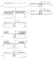
図1は、本実施例の半導体装置の構造を示す断面図である。本実施例の半導体装置では、シリコンウエハからなる半導体基板10上には素子形成部11が形成され、それぞれを貫通する貫通孔が形成され、貫通孔側壁には、絶縁性の金属酸化膜19が形成され、貫通孔内には、シード膜15を介して金属からなる導電材料16が充填されている。半導体基板10の裏面には裏面絶縁膜17が形成されている。 FIG. 1 is a cross-sectional view showing the structure of the semiconductor device of this example. In the semiconductor device of this embodiment, an
以下、図2(a)〜(g)を用いて、この半導体装置の製造方法について説明する。なお、図2(a)〜(g)は、本実施例の半導体装置の製造工程を示す断面図である。 Hereinafter, a method for manufacturing the semiconductor device will be described with reference to FIGS. 2A to 2G are cross-sectional views showing the manufacturing process of the semiconductor device of this example.
まず、図2(a)に示すように、半導体基板10の表面に素子形成部11を形成する。
次に、図2(b)に示すように、フォトレジストパターン12を形成し、フォトレジストパターン12をマスクとして用いて、反応性イオンエッチング(RIE)等の方法により素子形成部11及び半導体基板10を順次エッチングし、基板表面から100μm程度の孔13を形成する。この時の条件としては、素子形成部11のシリコン酸化膜は、CF4/O2系ガスでエッチングし、半導体基板10のシリコンは、SF6/O2系ガスでエッチングする。エッチング温度は、100℃以下とする。なお、本実施例では、孔13は、非貫通孔としているが、貫通孔としてもよい。First, as shown in FIG. 2A, the
Next, as shown in FIG. 2B, a
次に、図2(c)に示すように、素子形成部11上と孔13の側壁面にスパッタ法を用いてアルミニウム薄膜18を膜厚200〜10000Åで形成する。本実施例での具体的な成膜条件は、温度100℃以下で、印加電圧は3kW、ガス流量はアルゴン50SCCM、圧力0.4Paである。 Next, as shown in FIG. 2C, an aluminum
次に、図2(d)に示すように、素子形成部11上と孔13の側壁面に陽極酸化法を用いて陽極酸化膜19を形成する。陽極酸化法は、アルミニウム薄膜18の一端を直流電源の正極側を接続し、試料を3%リン酸アンモニウム溶液中に浸すことによって行う。このときの温度は、室温(10〜30℃程度)とする。直流電源の負極側には炭素棒を接続し、アルミニウム薄膜試料とは5cm程度の距離を隔てて同じ溶液中に浸す。陽極酸化膜の形成は、5〜50Vの電圧を印加して行う。アルミニウム薄膜18は、表面付近から徐々に酸化され、酸化反応が完全に進行するまで電圧を印加する。目標とする膜厚は200〜10000Åとする。 Next, as shown in FIG. 2D, an
次に、電気めっきの陰極となるシード膜15を陽極酸化膜19上に堆積する。そして、これを陰極として孔13の内部をCu16で充填する。さらに、CMPを用いて孔13以外のCu16とシード膜15と陽極酸化膜19を除去し、図2(e)に示す構造を得る。 Next, a
次に、図2(f)に示すように、半導体基板10の裏面を研削し、Cu16を裏面に露出させる。
次に、図2(g)に示すように、半導体基板10の裏面にSiNやSiO2等の裏面絶縁膜17を形成する。Next, as shown in FIG. 2F, the back surface of the
Next, as shown in FIG. 2G, a back insulating
本実施例の半導体装置の製造方法によれば、孔の側壁絶縁膜を室温で形成できるため素子への熱ダメージを抑制することが可能となる。 According to the method for manufacturing a semiconductor device of this embodiment, the sidewall insulating film of the hole can be formed at room temperature, so that thermal damage to the element can be suppressed.
以下、図3(a)〜(h)を用いて、実施例2の半導体装置の製造方法について説明する。なお、図3(a)〜(h)は、本実施例の半導体装置の製造工程を示す断面図である。
まず、図3(a)に示すように、半導体基板10の上面に素子形成部11を形成する。次に、図3(b)に示すように、フォトレジストパターン12を形成し、フォトレジストパターン12をマスクとして用いて、反応性イオンエッチング(RIE)等の方法により素子形成部11及び半導体基板10を順次エッチングし、基板表面から100μm程度の孔13を形成する。この時の条件は、素子形成部11のシリコン酸化膜は、CF4/O2系ガスでエッチングする。半導体基板10のシリコンは、SF6/O2系ガスでエッチングする。エッチング温度は、100℃以下とする。A method for manufacturing the semiconductor device of Example 2 will be described below with reference to FIGS. 3A to 3H are cross-sectional views showing the manufacturing process of the semiconductor device of this example.
First, as shown in FIG. 3A, the
次に、図3(c)に示すように、素子形成部11上と孔13の側壁面にスパッタ法を用いてアルミニウム薄膜18を膜厚200〜10000Å形成する。本実施例での具体的な成膜条件は、温度100℃以下で、印加電圧は3kW、ガス流量はアルゴン50SCCM、圧力0.4Paである。 Next, as shown in FIG. 3C, an aluminum
次に、図3(d)に示すように、アルミニウム薄膜18のうち配線として使用する領域18aを覆うフォトレジストパターン20を形成する。 Next, as shown in FIG. 3D, a
次に、図3(e)に示すように、アルミニウム薄膜18のうちフォトレジストパターン20で覆われていない領域と孔13の側壁面に、陽極酸化法を用いて陽極酸化膜19を形成する。アルミニウム薄膜18の一端に、直流電源の正極側を接続し、試料を3%リン酸アンモニウム溶液中に浸す。このときの温度は、室温(10〜30℃程度)とする。直流電源の負極側には、炭素棒を接続し、アルミニウム薄膜試料とは5cm程度の距離を隔てて同じ溶液中に浸す。陽極酸化膜の形成は、5〜50Vの電圧を印加して行う。アルミニウム薄膜18は、表面付近から徐々に酸化され、酸化反応が完全に進行するまで電圧を印加し続ける。この際、フォトレジストパターン20で覆われた領域18aのアルミニウム薄膜18は、溶液に浸されないので、陽極酸化されない。 Next, as shown in FIG. 3E, an
次に、フォトレジストパターン20を除去し、電気めっきの陰極となるシード膜15を陽極酸化膜19上に堆積する。そして、これを陰極として孔13の内部をCu16で充填する。さらに、CMPを用いて孔13以外のCu16とシード膜15と陽極酸化膜19を除去し、図3(f)に示す構造を得る。 Next, the
次に、図3(g)に示すように、半導体基板10の裏面を研削し、Cu16を裏面に露出させる。次に、図3(h)に示すように、半導体基板10の裏面にSiNやSiO2等の裏面絶縁膜17を形成する。Next, as shown in FIG. 3G, the back surface of the
本構造の半導体装置の製造方法によれば、追加の配線パターンを同時に形成することが可能となる。 According to the method for manufacturing a semiconductor device having this structure, it is possible to simultaneously form an additional wiring pattern.
以下、図4(a)〜(f)を用いて、実施例3の半導体装置の製造方法について説明する。なお、図3(a)〜(f)は、本実施例の半導体装置の製造工程を示す断面図である。 Hereinafter, a method for manufacturing the semiconductor device of Example 3 will be described with reference to FIGS. 3A to 3F are cross-sectional views showing the manufacturing process of the semiconductor device of this example.
まず、図4(a)に示すように、半導体基板10の上面に素子形成部11を形成する。次に、図4(b)に示すように半導体基板10の裏面側を後退させる。ここで半導体基板10の後退は、例えば機械研削、化学研磨、プラズマエッチング、又はガスエッチングなどの加工技術を用いて行う。処理条件は、例えば機械研削の場合、粗研削として#300程度の砥石を使用し研削後、仕上げ研削として#2000程度の砥石で研削を行う。後退後の半導体基板10の厚さは、実装の厚みを極力薄くするため、100μm以下、又は30〜50μmであることが望ましい。 First, as shown in FIG. 4A, the
半導体基板10の薄化に伴い、補強のため必要であれば補強板を半導体基板10の素子形成側に貼り付けておいてもよい。 As the
次に、図4(c)に示すように、半導体基板10の裏面側に、フォトレジストパターン12を形成し、フォトレジストパターン12をマスクとして用いて、反応性イオンエッチング(RIE)等の方法により半導体基板10及び素子形成部11を順次エッチングし、貫通孔13aを形成する。この時の条件は、半導体基板10のシリコンは、SF6/O2系ガスで、素子形成部11のシリコン酸化膜は、CF4/O2系ガスでエッチングする。エッチング温度は、100℃以下とする。Next, as shown in FIG. 4C, a
次に、図4(d)に示すように、半導体基板10の裏面側及び貫通孔13aの側壁面にスパッタ法を用いてアルミニウム薄膜18を膜厚200〜10000Å形成する。ここで本実施例の具体的な成膜条件は、温度が100℃以下で、印加電圧が3kW、ガス流量がアルゴン50SCCM、圧力0.4Paである。 Next, as shown in FIG. 4D, an aluminum
次に、図4(e)に示すように、半導体基板10の裏面と貫通孔13aの側壁面に陽極酸化法を用いて陽極酸化膜19を形成する。アルミニウム薄膜18の一端に、直流電源の正極側を接続し、試料を3%リン酸アンモニウム溶液中に浸す。このときの温度は、10〜30℃とする。直流電源の負極側には、炭素棒を接続し、アルミニウム薄膜試料とは5cm程度の距離を隔てて同じ溶液中に浸す。陽極酸化膜の形成は、5〜50Vの電圧を印加する。アルミニウム薄膜18は、表面付近から徐々に酸化され、酸化反応が完全に進行するまで電圧を印加し続ける。 Next, as shown in FIG. 4E, an
次に、電気めっきの陰極となるシード膜15を陽極酸化膜19上に堆積する。そして、これを陰極として貫通孔13aの内部をCu16で充填する。さらに、CMPを用いて貫通孔13a以外のCu16とシード膜15を除去し、図4(f)に示す構造を得る。この時、半導体基板10の裏面に形成されている陽極酸化膜19は、除去せず残しておく。 Next, a
本構造の半導体装置の製造方法によれば、貫通孔側壁絶縁膜を裏面絶縁膜と同時に形成できるため工程の簡略化が可能となる。 According to the manufacturing method of the semiconductor device having this structure, the through-hole side wall insulating film can be formed simultaneously with the back surface insulating film, so that the process can be simplified.
10 半導体基板
11 素子形成部
12、20 フォトレジストパターン
13 孔
13a 貫通孔
14 絶縁膜
15 シード膜
16 金属、Cu
17 裏面絶縁膜
18 アルミニウム薄膜
19 陽極酸化膜DESCRIPTION OF
17 Back
Claims (9)
Translated fromJapanesePriority Applications (3)
| Application Number | Priority Date | Filing Date | Title |
|---|---|---|---|
| JP2005079638AJP4199206B2 (en) | 2005-03-18 | 2005-03-18 | Manufacturing method of semiconductor device |
| EP06251390AEP1703553A3 (en) | 2005-03-18 | 2006-03-15 | Via in semiconductor substrate and its fabrication method |
| US11/376,089US20060211269A1 (en) | 2005-03-18 | 2006-03-16 | Semiconductor device and its fabrication method |
Applications Claiming Priority (1)
| Application Number | Priority Date | Filing Date | Title |
|---|---|---|---|
| JP2005079638AJP4199206B2 (en) | 2005-03-18 | 2005-03-18 | Manufacturing method of semiconductor device |
Publications (2)
| Publication Number | Publication Date |
|---|---|
| JP2006261553A JP2006261553A (en) | 2006-09-28 |
| JP4199206B2true JP4199206B2 (en) | 2008-12-17 |
Family
ID=36572246
Family Applications (1)
| Application Number | Title | Priority Date | Filing Date |
|---|---|---|---|
| JP2005079638AExpired - Fee RelatedJP4199206B2 (en) | 2005-03-18 | 2005-03-18 | Manufacturing method of semiconductor device |
Country Status (3)
| Country | Link |
|---|---|
| US (1) | US20060211269A1 (en) |
| EP (1) | EP1703553A3 (en) |
| JP (1) | JP4199206B2 (en) |
Families Citing this family (8)
| Publication number | Priority date | Publication date | Assignee | Title |
|---|---|---|---|---|
| WO2008002670A2 (en)* | 2006-06-29 | 2008-01-03 | Icemos Technology Corporation | Varying pitch adapter and a method of forming a varying pitch adapter |
| US7544605B2 (en)* | 2006-11-21 | 2009-06-09 | Freescale Semiconductor, Inc. | Method of making a contact on a backside of a die |
| WO2009111874A1 (en) | 2008-03-11 | 2009-09-17 | The Royal Institution For The Advancement Of Learning/ Mcgiil University | Low-temperature wafer level processing for mems devices |
| JP5528430B2 (en)* | 2008-05-02 | 2014-06-25 | アイメック | Formation method of oxide layer |
| KR20100079200A (en)* | 2008-12-30 | 2010-07-08 | 주식회사 동부하이텍 | Method for manufacturing of semiconductor device |
| TWI604624B (en)* | 2010-05-11 | 2017-11-01 | 荷蘭能源研究基金會 | Solar cell and preparation method thereof |
| NL2004698C2 (en)* | 2010-05-11 | 2011-11-15 | Stichting Energie | Solar cell and method of manufacturing such a solar cell. |
| US10373930B2 (en)* | 2012-08-10 | 2019-08-06 | Cyntec Co., Ltd | Package structure and the method to fabricate thereof |
Family Cites Families (7)
| Publication number | Priority date | Publication date | Assignee | Title |
|---|---|---|---|---|
| JPS5217995B2 (en)* | 1972-02-18 | 1977-05-19 | ||
| US5098860A (en)* | 1990-05-07 | 1992-03-24 | The Boeing Company | Method of fabricating high-density interconnect structures having tantalum/tantalum oxide layers |
| US6809421B1 (en)* | 1996-12-02 | 2004-10-26 | Kabushiki Kaisha Toshiba | Multichip semiconductor device, chip therefor and method of formation thereof |
| JP4011695B2 (en)* | 1996-12-02 | 2007-11-21 | 株式会社東芝 | Chip for multi-chip semiconductor device and method for forming the same |
| JP3974284B2 (en)* | 1999-03-18 | 2007-09-12 | 株式会社東芝 | Manufacturing method of semiconductor device |
| JP3648480B2 (en)* | 2001-12-26 | 2005-05-18 | 株式会社東芝 | Semiconductor device and manufacturing method thereof |
| US6897148B2 (en)* | 2003-04-09 | 2005-05-24 | Tru-Si Technologies, Inc. | Electroplating and electroless plating of conductive materials into openings, and structures obtained thereby |
- 2005
- 2005-03-18JPJP2005079638Apatent/JP4199206B2/ennot_activeExpired - Fee Related
- 2006
- 2006-03-15EPEP06251390Apatent/EP1703553A3/ennot_activeWithdrawn
- 2006-03-16USUS11/376,089patent/US20060211269A1/ennot_activeAbandoned
Also Published As
| Publication number | Publication date |
|---|---|
| EP1703553A3 (en) | 2006-11-08 |
| US20060211269A1 (en) | 2006-09-21 |
| JP2006261553A (en) | 2006-09-28 |
| EP1703553A2 (en) | 2006-09-20 |
Similar Documents
| Publication | Publication Date | Title |
|---|---|---|
| CN100481380C (en) | Method for manufacturing interconnect structure in semiconductor device | |
| US7932175B2 (en) | Method to form a via | |
| US20120119216A1 (en) | Semiconductor Device, Method of Manufacturing A Semiconductor Device, and Display Device | |
| TW200845347A (en) | Chip carrier substrate including capacitor and method for fabrication thereof | |
| JP2004022990A (en) | Method for plugging through hole of silicon substrate | |
| US20130319734A1 (en) | Package substrate and method of manufacturing the same | |
| TWI546845B (en) | Semiconductor device and method of forming same | |
| US20060211269A1 (en) | Semiconductor device and its fabrication method | |
| US10141224B2 (en) | Manufacturing method of interconnection structure | |
| US7036219B2 (en) | Method for manufacturing a high-efficiency thermal conductive base board | |
| JP3873133B2 (en) | Capacitor structure | |
| US6384484B1 (en) | Semiconductor device | |
| JP2013524019A (en) | Seed layer deposition in microscale structures | |
| EP1587348A1 (en) | Conductive base board | |
| JP2006222138A (en) | Method for forming through-electrode | |
| KR101913843B1 (en) | Method for forming via contact | |
| CN107154380B (en) | Preparation method of metal interconnection structure | |
| US20150028488A1 (en) | Method for manufacturing a conducting contact on a conducting element | |
| US8883632B2 (en) | Manufacturing method and manufacturing apparatus of device | |
| JP2012253333A (en) | Wiring board having through electrode, and manufacturing method of the same | |
| US20030098767A1 (en) | Process for fabricating an electronic component incorporating an inductive microcomponent | |
| JPH11251436A (en) | Method for forming conductive part in integrated circuit | |
| KR101913842B1 (en) | Method for forming via contact | |
| KR100467803B1 (en) | Fabrication method of semiconductor device | |
| JP2005294655A (en) | Method of manufacturing profile including conductive layer on its surface, and heatsink |
Legal Events
| Date | Code | Title | Description |
|---|---|---|---|
| A977 | Report on retrieval | Free format text:JAPANESE INTERMEDIATE CODE: A971007 Effective date:20080215 | |
| A131 | Notification of reasons for refusal | Free format text:JAPANESE INTERMEDIATE CODE: A131 Effective date:20080715 | |
| A521 | Written amendment | Free format text:JAPANESE INTERMEDIATE CODE: A523 Effective date:20080903 | |
| TRDD | Decision of grant or rejection written | ||
| A01 | Written decision to grant a patent or to grant a registration (utility model) | Free format text:JAPANESE INTERMEDIATE CODE: A01 Effective date:20080930 | |
| A01 | Written decision to grant a patent or to grant a registration (utility model) | Free format text:JAPANESE INTERMEDIATE CODE: A01 | |
| A61 | First payment of annual fees (during grant procedure) | Free format text:JAPANESE INTERMEDIATE CODE: A61 Effective date:20081002 | |
| FPAY | Renewal fee payment (event date is renewal date of database) | Free format text:PAYMENT UNTIL: 20111010 Year of fee payment:3 | |
| R150 | Certificate of patent or registration of utility model | Free format text:JAPANESE INTERMEDIATE CODE: R150 | |
| FPAY | Renewal fee payment (event date is renewal date of database) | Free format text:PAYMENT UNTIL: 20121010 Year of fee payment:4 | |
| FPAY | Renewal fee payment (event date is renewal date of database) | Free format text:PAYMENT UNTIL: 20131010 Year of fee payment:5 | |
| LAPS | Cancellation because of no payment of annual fees |