JP4192327B2 - Information processing apparatus and method, and providing medium - Google Patents
Information processing apparatus and method, and providing mediumDownload PDFInfo
- Publication number
- JP4192327B2 JP4192327B2JP07725499AJP7725499AJP4192327B2JP 4192327 B2JP4192327 B2JP 4192327B2JP 07725499 AJP07725499 AJP 07725499AJP 7725499 AJP7725499 AJP 7725499AJP 4192327 B2JP4192327 B2JP 4192327B2
- Authority
- JP
- Japan
- Prior art keywords
- signal
- backlight
- dimming
- lcd
- dimming signal
- Prior art date
- Legal status (The legal status is an assumption and is not a legal conclusion. Google has not performed a legal analysis and makes no representation as to the accuracy of the status listed.)
- Expired - Fee Related
Links
- 238000000034methodMethods0.000titleclaimsdescription31
- 230000010365information processingEffects0.000titleclaimsdescription12
- 238000012546transferMethods0.000claimsdescription19
- 238000012545processingMethods0.000claimsdescription18
- 238000000605extractionMethods0.000claimsdescription11
- 238000003672processing methodMethods0.000claimsdescription4
- 230000008054signal transmissionEffects0.000description26
- 230000005540biological transmissionEffects0.000description16
- 238000006243chemical reactionMethods0.000description6
- 210000000078clawAnatomy0.000description6
- 230000006870functionEffects0.000description5
- 238000003384imaging methodMethods0.000description5
- 238000004891communicationMethods0.000description4
- 208000032365Electromagnetic interferenceDiseases0.000description3
- 230000004913activationEffects0.000description3
- 238000010586diagramMethods0.000description3
- 239000000284extractSubstances0.000description2
- 230000002093peripheral effectEffects0.000description2
- 238000004590computer programMethods0.000description1
- 230000000694effectsEffects0.000description1
- 238000005516engineering processMethods0.000description1
- 239000004973liquid crystal related substanceSubstances0.000description1
- 230000010355oscillationEffects0.000description1
- 230000011664signalingEffects0.000description1
- 230000005236sound signalEffects0.000description1
- 239000002699waste materialSubstances0.000description1
Images


Landscapes
- Communication Control (AREA)
- Liquid Crystal Display Device Control (AREA)
- Control Of Indicators Other Than Cathode Ray Tubes (AREA)
- Dc Digital Transmission (AREA)
Description
Translated fromJapanese【0001】
【発明の属する技術分野】
本発明は、情報処理装置及び方法、並びに提供媒体に関し、特に、画像データの送信時に、画像データとは異なる信号を送信する情報処理装置及び方法、並びに提供媒体に関する。
【0002】
【従来の技術】
最近のデータ転送技術として、LVDS(Low Voltage Differential Signaling)が、一般的に普及しつつある。LVDSは、低電圧差動方式の信号送信方式であり、高速で大容量(約530Mbps乃至1365Mbps)のデータ転送が可能である。LVDS方式は、低電圧差動方式であるため、EMI(Electro-Magnetic Interference)による影響を小さくできるので、特に、EMIの影響を受けやすいディスプレイへの画像情報の転送などに最適である。
【0003】
【発明が解決しようとする課題】
ところで、転送する画像情報には、同期信号が含まれており、その伝送方式には、2つの方式がある。伝送方式の1つは、1ビットのイネーブル信号に、水平同期信号と垂直同期信号を多重化して伝送する方式であり、もう1つの伝送方式は、水平同期信号と垂直同期信号を各々分けて2ビットで伝送する方式である。
【0004】
この同期信号の伝送方式は、システムによって静的に決まるものであるが、LVDSには、水平同期信号、垂直同期信号、およびイネーブル信号のそれぞれについて1ビットずつ確保され、どちらの同期信号の伝送方式にも対応できるようになされている。
【0005】
このため、例えば、パーソナルコンピュータの本体からLVDS方式で画像情報をディスプレイに転送し、画像を表示させるようにした場合、水平同期信号と垂直同期信号を多重化して1ビットのイネーブル信号で同期信号を伝送する方式を用いると、水平同期信号と垂直同期信号の2ビットの送信されていない余剰ビットが発生し、水平同期信号と垂直同期信号の各々を2ビットで伝送する同期信号の伝送方式を用いると、イネーブル信号の1ビットの送信されていない余剰ビットが発生するという課題があった。
【0006】
また、例えば、ディスプレイ近傍に、ディスプレイ以外にパーソナルコンピュータによって駆動させる駆動装置があった場合、上述のような余剰ビットがあるにも拘わらず、その駆動装置専用の信号線およびインターフェースを設けなければならないという課題があった。
【0007】
本発明は、このような状況に鑑みてなされたものであり、LVDS方式により画像データを転送する際に、画像データと合わせて、画像データと異なる信号を送信させることにより、効果的に、かつ、省スペースで、データを転送することができるようにするものである。
【0008】
【課題を解決するための手段】
請求項1に記載の情報処理装置は、複数ビットの画像データの信号が複数の所定の信号線を占有すると予測される時刻とは異なる時刻に、所定の信号線に、調光信号であることを表すフラグを付けたLCDのバックライトの調光信号を重畳する重畳手段と、所定の信号線の信号をLCDと前記バックライトを含む表示手段に転送する転送手段とを備え、前記表示手段は、さらに、前記転送手段により転送された信号から、前記フラグが付けられた前記調光信号を抽出する抽出手段と、前記抽出手段により抽出された前記調光信号を前記バックライトに出力し、前記バックライトの明るさを調整する調整手段とを有する。
【0009】
請求項2に記載の情報処理方法は、複数ビットの画像データの信号が複数の所定の信号線を占有すると予測される時刻とは異なる時刻に、所定の信号線に、調光信号であることを表すフラグを付けたLCDのバックライトの調光信号を重畳する重畳ステップと、所定の信号線の信号をLCDと前記バックライトを含む表示手段に転送する転送ステップと、前記転送ステップの処理により転送された信号から、前記フラグが付けられた前記調光信号を抽出する抽出ステップと、前記抽出ステップの処理により抽出された前記調光信号を前記バックライトに出力し、前記バックライトの明るさを調整する調整ステップとを含む。
【0010】
請求項3に記載の提供媒体は、複数ビットの画像データの信号が複数の所定の信号線を占有すると予測される時刻とは異なる時刻に、所定の信号線に、調光信号であることを表すフラグを付けたLCDのバックライトの調光信号を重畳する重畳ステップと、所定の信号線の信号をLCDと前記バックライトを含む表示手段に転送する転送ステップと、前記転送ステップの処理により転送された信号から、前記フラグが付けられた前記調光信号を抽出する抽出ステップと、前記抽出ステップの処理により抽出された前記調光信号を前記バックライトに出力し、前記バックライトの明るさを調整する調整ステップとを含む処理を実行させるコンピュータが読み取り可能なプログラムを提供する。
【0011】
請求項1に記載の情報処理装置、請求項2に記載の情報処理方法、および請求項3に記載の提供媒体においては、複数ビットの画像データの信号が複数の所定の信号線を占有すると予測される時刻とは異なる時刻に、所定の信号線に、調光信号であることを表すフラグを付けたLCDのバックライトの調光信号が重畳され、所定の信号線の信号がLCDと前記バックライトを含む表示手段に転送される。また、転送された信号から、前記フラグが付けられた前記調光信号が抽出され、抽出された前記調光信号が前記バックライトに出力され、前記バックライトの明るさが調整される。
【0012】
【発明の実施の形態】
以下、本発明の情報処理装置の一実施の形態を図面を参照して説明する。
【0013】
図1乃至図6は、本発明を適用した携帯型パーソナルコンピュータの構成例を表している。このパーソナルコンピュータ1は、ミニノート型のパーソナルコンピュータとされ、基本的に、本体2と、本体2に対して開閉自在とされている表示部3により構成されている。図1は、表示部3を本体2に対して開いた状態を示す外観斜視図、図2は、図1の平面図、図3は、表示部3を本体2に対して閉塞した状態を示す左側側面図、図4は、表示部3を本体2に対して180度開いた状態を示す右側側面図、図5は、図3の正面図、図6は、図4の底面図である。 本体2には、各種の文字や記号などを入力するとき操作されるキーボード4、マウスカーソルを移動するさせるときなどに操作されるトラックポイント(商標)5が、その上面に設けられている。また、本体2の上面には、音を出力するスピーカ8と、表示部3に設けられているCCDビデオカメラ23で撮像するとき操作されるシャッタボタン10がさらに設けられている。
【0014】
表示部3の上端部には、ツメ13が設けられており、図3に示すように、表示部3を本体2に対して閉塞した状態において、ツメ13に対向する位置における本体2には、ツメ13が嵌合する孔部6が設けられている。本体2の前面には、スライドレバー7が前面に平行に移動可能に設けられており、スライドレバー7は孔部6に嵌合したツメ13と係合してロックし、またロック解除することができるようになっている。ロックを解除することにより、表示部3を本体2に対して回動することができる。ツメ13の隣には、マイクロホン24が取り付けられている。このマイクロホン24は、図6にも示すように、背面からの音も収音できるようになされている。
【0015】
本体2の正面にはまた、プログラマブルパワーキー(PPK)9が設けられている。本体2の右側面には、図4に示すように、排気孔11が設けられており、本体2の前面下部には、図5に示すように、吸気孔14が設けられている。さらに、排気孔11の右側には、PCMCIA(Personal Comuputer Memory Card International Association)カード(PCカード)を挿入するためのスロット12が設けられている。
【0016】
表示部3の正面には、画像を表示するLCD(Liquid Crystal Display)21が設けられており、その上端部には、撮像部22が、表示部3に対して回動自在に設けられている。すなわち、この撮像部22は、LCD21と同一の方向と、その逆の方向(背面の方向)との間の180度の範囲の任意の位置に回動することができるようになされている。撮像部22には、CCDビデオカメラ23が取り付けられている。
【0017】
表示部3の下側の本体側には、電源ランプPL、電池ランプBL、メッセージランプML、その他のLEDよりなるランプが設けられている。尚、図3に示す符号31は、本体2の左側面に設けられた電源スイッチであり、図5に示す符号25は、CCDビデオカメラ23のフォーカスを調整する調整リングである。さらに、図6に示す符号26は、本体2内に増設メモリを取り付けるための開口部を被覆する蓋であり、符号41は、蓋26のロックツメを外すためのピンを挿入する小孔である。 図7は、パーソナルコンピュータ1の内部の構成を表している。内部(PCI(Peripheral Componet Interconnect))バス51には、CPU(Central Processing Unit)52、必要に応じて挿入されるPCカード53、RAM(Random Access Memory)54、およびグラフィックチップ81が接続されている。この内部バス51は、外部(ISA(Industrial Standard Architecture))バス55に接続されており、外部バス55には、ハードディスクドライブ(HDD)56、I/O(入出力)コントローラ57、キーボードコントローラ58、トラックポイントコントローラ59、サウンドチップ60、LCDコントローラ83、モデム50などが接続されている。
【0018】
CPU52は、各機能を統括するコントローラであり、PCカード53は、オプションの機能を付加するとき適宜装着される。
【0019】
RAM54の中には、起動が完了した時点において、電子メールプログラム(アプリケーションプログラム)54A、オートパイロットプログラム(アプリケーションプログラム)54B、そしてOS(基本プログラム)54CがHDD56から転送され、記憶される。
【0020】
電子メールプログラム54Aは、電話回線のような通信回線などからネットワーク経由で通信文を授受するプログラムである。電子メールプログラム54Aは、特定機能としての着信メール取得機能を有している。この着信メール取得機能は、メールサーバ93に対して、そのメールボックス93A内に自分(利用者)宛のメールが着信しているかどうかを確認して、自分宛のメールがあれば取得する処理を実行する。
【0021】
オートパイロットプログラム54Bは、予め設定された複数の処理(またはプログラム)などを、予め設定された順序で順次起動して、処理するプログラムである。
【0022】
OS(基本プログラムソフトウェア)54Cは、Windows95あるいはWindows98(商標)に代表される、コンピュータの基本的な動作を制御するものである。
【0023】
一方、外部バス55側のハードディスクドライブ(HDD)56には、電子メールプログラム56A、オートパイロットプログラム56B、OS(基本プログラムソフトウェア)56Cが記憶されている。ハードディスクドライブ56内のOS56C、オートパイロットプログラム56B、および電子メールプログラム56Aは、起動(ブートアップ)処理の過程で、RAM54内に順次転送され、格納される。
【0024】
I/Oコントローラ57は、マイクロコントローラ61を有し、このマイクロコントローラ61には、I/Oインタフェース62が設けられている。このマイクロコントローラ61内では、I/Oインタフェース62、CPU63、RAM64、ROM69が相互に接続されて構成されている。このRAM64は、キー入力ステイタスレジスタ65、LED(発光ダイオード)制御レジスタ66、設定時刻レジスタ67、レジスタ68を有している。設定時刻レジスタ67は、ユーザが予め設定した時刻(起動条件)になると起動シーケンス制御部76の動作を開始させる際に利用される。レジスタ68は、予め設定された操作キーの組み合わせ(起動条件)と、起動すべきアプリケーションプログラムの対応を記憶するもので、その記憶された操作キーの組み合わせがユーザにより入力されると、その記憶されたアプリケーションプログラム(例えば電子メール)が起動されることになる。
【0025】
キー入力ステイタスレジスタ65は、ワンタッチ操作用のプログラマブルパワーキー(PPK)9が押されると、操作キーフラグが格納されるようになっている。LED制御レジスタ66は、レジスタ68に記憶されたアプリケーションプログラム(電子メール)の立上げ状態を表示するメッセージランプMLの点灯を制御するものである。設定時刻レジスタ67は、所定の時刻を任意に設定することができるものである。
【0026】
なお、このマイクロコントローラ61には、バックアップ用のバッテリ74が接続されており、各レジスタ65,66,67の値は、本体2の電源がオフとされている状態においても保持されるようになっている。
【0027】
マイクロコントローラ61内のROM69の中には、ウェイクアッププログラム70、キー入力監視プログラム71、LED制御プログラム72が予め格納されている。このROM69は、例えばEEPROM(electrically erasable and programmable read only memory)で構成されている。このEEPROMはフラッシュメモリとも呼ばれている。さらにマイクロコントローラ61には、常時現在時刻をカウントするRTC(Real-Time Clock)75が接続されている。
【0028】
ROM69の中のウェイクアッププログラム70は、RTC75から供給される現在時刻データに基づいて、設定時刻レジスタ67に予め設定された時刻になったかどうかをチェックして、設定された時刻になると、所定の処理(またはプログラム)などの起動をするプログラムである。キー入力監視プログラム71は、PPK9が利用者により押されたかどうかを常時監視するプログラムである。LED制御プログラム72は、メッセージランプMLの点灯を制御するプログラムである。
【0029】
ROM69には、さらにBIOS(Basic Input/Output System)73が書き込まれている。このBIOSとは、基本入出力システムのことをいい、OSやアプリケーションソフトウェアと周辺機器(ディスプレイ、キーボード、ハードディスクドライブなど)の間でのデータの受け渡し(入出力)を制御するソフトウェアプログラムである。
【0030】
外部バス55に接続されているキーボードコントローラ58は、キーボード4からの入力をコントロールする。トラックポイントコントローラ59は、トラックポイント5の入力を制御する。
【0031】
サウンドチップ60は、マイクロホン24からの入力を取り込み、あるいは内蔵スピーカ8に対して音声信号を供給する。
【0032】
モデム50は、公衆電話回線90、インターネットサービスプロバイダ91を介して、インターネットなどの通信ネットワーク92やメールサーバ93などに接続することができる。
【0033】
内部バス51に接続されているグラフィックチップ81には、CCDビデオカメラ23で取り込んだ画像データが、処理部82で処理された後、入力されるようになされている。グラフィックチップ81は、処理部82を介してCCDビデオカメラ23より入力されたビデオデータを、内蔵するVRAM81Aに記憶し、適宜、これを読み出して、LCDコントローラ83に出力する。LCDコントローラ83は、グラフィックチップ81より供給された画像データ(TTL(Transistor-Transistor Logic)信号)をLVDSドライバ85に出力する。また、PWM(Pulse Width Modulation)回路84は、I/Oコントローラ57から外部バス55を介して送られてくるバックライト88を制御する調光信号を受け取り、これをPWMデータに変換した後、LVDSドライバ85に出力する。LCDコントローラ83からの画像データとPWM回路84からの調光信号をTTL信号で受信したLVDSドライバ85は、受信したTTL信号を後述するLVDS信号に変換し、表示部3に出力する。
【0034】
LVDSドライバ85から送信されたLVDS信号は、表示部3のLVDSレシーバ86によって再びTTL信号に変換され、変換された画像データは、LCD21に出力され、表示される。LVDSレシーバ86から出力された調光信号は、平均値回路87によってアナログ化された後、バックライト88に出力され、バックライト88が、LCD21を後方から照明するようになされている。
【0035】
電源スイッチ31は、電源をオンまたはオフするとき操作される。半押しスイッチ32は、シャッタボタン10が半押し状態にされたときオンされ、全押しスイッチ33は、シャッタボタン10が全押し状態にされたときオンされる。反転スイッチ34は、撮像部22が180度回転されたとき(CCDビデオカメラ23がLCD21の反対側を撮像する方向に回転されたとき)、オンされるようになされている。
【0036】
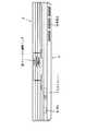
図8は、本体2のLVDSドライバ85から表示部3のLVDSレシーバ86に画像データを伝送する部分の詳細な構成例を示している。グラフィックチップ81は、画像データ(TTL信号)を発生し、LCDコントローラ83に出力する。画像データには、赤色信号、緑色信号、青色信号、水平同期信号、垂直同期信号、イネーブル信号、およびクロック信号が含まれている。
【0037】
LCDコントローラ83は、赤色信号、緑色信号、および青色信号について、赤色信号発信部101、緑色信号発信部102、および青色信号発信部103から各々6ビットのデータTxIN0乃至TxIN5,TxIN6乃至TxIN11,TxIN12乃至TxIN17を出力し、並列に(従って、合計18ビットのデータとして)LVDSドライバ85に送信する。
【0038】
また、LCDコントローラ83は、水平同期信号、垂直同期信号、イネーブル信号、およびクロック信号を、各々水平同期信号発信部104、垂直同期信号発信部105、イネーブル信号発信部106およびクロック信号発信部107から1ビットのデータTxIN18,TxIN19,TxIN20として出力し、LVDSドライバ85に送信する。
【0039】
LVDSドライバ85は、信号切替装置111、信号変換装置112、PLL(Phase Locked Loop)回路113、および差動信号発信回路114乃至117を有している。
【0040】
信号切替装置111は、同期信号の伝送方式によって動作が異なる。同期信号の伝送方式は、水平同期信号と垂直同期信号を多重化し、イネーブル信号1ビットのみで同期信号を伝送する方式か、あるいは水平同期信号と垂直同期信号の各々を2ビットで同期信号を伝送する方式のいずれかである。
【0041】
同期信号の伝送方式が、上述の前者であった場合(イネーブル信号1ビットのみの場合)、信号切替装置111は、イネーブル信号発信部106からのイネーブル信号をそのまま、信号変換装置112に転送すると共に、信号が転送されない水平同期信号発信部104および垂直同期信号発信部105からの信号線(計2ビット)に、PWM回路84から送信されてくる調光信号に調光信号であることを示すフラグを付けて供給し、信号変換装置112に送る。
【0042】
また、同期信号の伝送方式が、上述の後者であった場合(水平同期信号と垂直同期信号の2ビットの場合)、信号切替装置111は、水平同期信号発信部104および垂直同期信号発信部105からの信号をそのまま、信号変換装置112に転送すると共に、信号が転送されていないイネーブル信号発信部106からの信号線(1ビット)にPWM回路84から送信されてくる調光信号に調光信号であることを示すフラグを付けて供給し、信号変換装置112に送る。
【0043】
尚、信号切替装置111は、水平同期信号発信部104、垂直同期信号発信部105およびイネーブル信号発信部106からの電源投入後最初に入力される信号の有無によって同期信号の伝送方式を判定し、以降はその判定された上記いずれかの同期信号の伝送方式に対応した処理が実行される。
【0044】
信号変換装置112は、赤色信号発信部101、緑色信号発信部102、青色信号発信部103、および信号切替装置111から並列に送られてくる合計21ビットの信号を受信し、3つの信号に変換し、差動信号発信回路114乃至116に出力する。
【0045】
PLL回路113は、クロック信号発信部107から送られてくるクロック信号(TxCLKIN)に対して内部の発振回路の出力位相を同期させ、内部クロックとの間に生じる時間差を回路的に制御して調整し、高速なクロックアクセス時間や高速の動作周波数を実現する。このPLL回路113によって、発生されたクロック信号は、差動信号発信回路117に供給され、差動信号発信回路117は、差動信号としてのクロック信号(R1CLKIN+およびR1CLKIN-)を表示部3に出力する。
【0046】
差動信号発信回路114乃至117は、受信した信号を差動信号に変換して出力する。この差動信号は、絶対値が同じで、逆極性の2つの信号とされている。例えば、入力値が1Vであった場合、差動信号発信回路114乃至117は、1Vの信号と−1Vの信号の2つの信号を発生する。また、受信する場合、後述する差動信号受信回路124乃至127は、1Vの信号と−1Vの信号の差をとり、2で除する演算((1−(−1))/2=1)を行う。
【0047】
上述の様に転送することによって、ノイズに対して強い信号の転送が可能となる。すなわち、例えば1Vの信号を送信した場合に生じたノイズが、αVであった場合、受信側は、(1+α)Vと(−1+α)Vの信号を受信することになる。このときに上述のように差をとって2で除する(((1+α)−(−1+α))/2=1)ことによってノイズは、打ち消されるので、ノイズに対して強い信号の送受信が可能となる。
【0048】
この様にLVDSドライバ85は、TxIN0乃至TxIN20とTxCLKINの合計22ビットの並列信号を4つの信号として表示部3に出力する。
【0049】
図9は、信号変換装置112が、受信した信号を3つの信号に変換し、差動信号発信回路114乃至116から出力させる際の送信信号(LVDS信号)に対する入力信号(TTL信号)の配置の例を示している。図9の例では、赤色信号発信部101、緑色信号発信部102、および青色信号発信部103が出力する赤色信号TxIN0乃至TxIN5、緑色信号TxIN6乃至TxIN11、および青色信号TxIN12乃至TxIN17が、それぞれ1クロックの周期内にシリアルに配置されている。
【0050】
水平同期信号と垂直同期信号がそれぞれ1ビットずつを用いて送られる場合、TxIN18,TxIN19が用いられ、最後の1ビットTxIN20は、余剰ビットとなる。水平同期信号と垂直同期信号が、多重化され、1ビットのイネーブル信号として送られる場合、TxIN20が用いられ、TxIN18,TxIN19の2ビットは余剰ビットとなる。この余剰ビットを用いて、調光信号が送られる。
【0051】
PWM回路84は、入力される調光信号をPWMデータにパルス化し、LVDSドライバ85の信号切替装置111に出力する。図10は、PWM回路84に入力される信号とクロック信号に基づいて生成され、出力される信号を示している。尚、説明の便宜上、外部バス55を介して入力される入力信号(図10(A))は、アナログ信号として示されている。
【0052】
外部バス55を介して、図10(A)に示されるような入力信号が入力されると、クロック信号発信部107より入力される。図10(B)に示されるクロック信号に同期して、図10(C)に示されるように信号が出力される。図10に示されるように、入力信号のレベルが低い(調光を暗くする)場合は、出力信号のパルス幅が狭くなり、逆に、入力信号レベルが高い(調光を明るくする)場合、出力信号のパルス幅が、広くなる。これによって、後述するバックライト88の明るさが調整される。
【0053】
LVDSドライバ85から送信されてくる4つの信号(実際には8本の信号線からの信号)は、差動信号受信回路124乃至127によって受信される。受信された信号は、各々の差動信号受信回路で上述のように、対となる信号と差がとられ、2で除された後、信号変換装置122およびPLL回路123に出力される。
【0054】
信号変換装置122は、受信された3つの信号(LVDS信号)を、TTL信号に変換する。変換されたTTL信号は、LVDSドライバ85の信号変換装置112に入力された信号TxIN0乃至TxIN20に対応する信号RxOUT0乃至RxOUT20として出力される。赤色信号として出力された信号RxOUT0乃至RxOUT5は、LCD21の赤色信号受信部131に、緑色信号として出力された信号RxOUT6乃至RxOUT11は、緑色信号受信部132に、青色信号として出力された信号RxOUT12乃至RxOUT17は、青色信号受信部133に、それぞれ出力される。水平同期信号、垂直同期信号、イネーブル信号、および調光信号として出力される信号RxOUT18乃至RxOUT20は、信号切替装置121に出力される。
【0055】
信号切替装置121は、受信した信号RxOUT18乃至RxOUT20の中から調光信号のフラグのついた調光信号のみを抽出し、平均値回路87に出力する。それ以外の信号は、垂直同期信号、水平同期信号、またはイネーブル信号とみなして、それぞれを、水平同期信号受信部134、垂直同期信号受信部135、またはイネーブル信号受信部136に出力する。
【0056】
平均値回路87に入力された調光信号は、平均値回路87によって、パルス化された信号からアナログ信号に変換され、バックライト88に出力される。
【0057】
PLL回路123に入力された信号は、LVDSドライバ85のPLL回路113に入力されたクロック信号TxCLKINに対応するクロック信号RxCLKOUTに復調され、クロック信号受信部137に出力される。
【0058】
LCD21は、上述のように赤色信号受信部131、緑色信号受信部132、青色信号受信部133、水平同期信号受信部134、垂直同期信号受信部135、イネーブル信号受信部136、およびクロック信号受信部137のそれぞれで受信されたTTL信号に基づいて、画像データを表示する。
【0059】
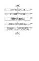
次に、図11のフローチャートを参照して、本体2のCPU63(またはCPU52)が、画像データと共に調光信号を表示部3に送信するときの動作について説明する。CPU63は、ステップS11において、外部バス55を介してPWM回路84に、調光信号を出力する。PWM回路84は、LCDコントローラ83のクロック信号発信部107からクロック信号を受信すると共に、CPU63から受信した調光信号を図10(C)に示すようにPWMデータにパルス化し、信号切替装置111に出力する。
【0060】
信号切替装置111は、ステップS12において、パルス化された調光信号を受信し、ステップS13において、使用されていない信号線に、PWM回路84から送られてきた調光信号に調光信号のフラグを付けて供給し、信号変換装置112に送信する。上述の同期信号の伝送方式によって、使用されていない信号線は、水平同期信号および垂直同期信号の2ビットの信号線か、または、イネーブル信号の1ビットの信号線である。
【0061】
ステップS14において、信号変換装置112は、受信した全てのTTL信号をLVDS信号に変換し、差動信号発信装置114乃至116を介して表示部3に送信し、本体2の処理は終了する。
【0062】
次に、図12を参照して、表示部3の動作について説明する。LVDSドライバ85からのLVDS信号を受信すると処理が開始され、ステップS21において、信号変換装置122は、受信した全てのLVDS信号を、TTL信号に変換し、出力する。ステップS22において、信号切替装置121は、信号変換装置122から出力されたTTL信号を受信する。
【0063】
ステップS23において、信号切替装置121は、受信したTTL信号の中から、調光信号のフラグを持つ、調光信号を抽出する。そして、信号切替装置121は、ステップS24において、この抽出した調光信号だけを平均値回路87に転送する。尚、調光信号のフラグを持たない信号は、水平同期信号、垂直同期信号、またはイネーブル信号とみなされ、それぞれ、水平同期信号受信部134、垂直同期信号受信部135、またはイネーブル信号受信部136に出力される。
【0064】
ステップS25において、平均値回路87は、受信したパルス化された調光信号をアナログ化し、バックライト88に出力する。バックライト88は、受信した調光信号に基づいた明るさに調整され、その明るさで、LCD21を後方から照明し、表示部3の処理は終了される。
【0065】
尚、この例においては画像情報とは異なる信号として調光信号を送信したが、表示部3に、LCD21以外に、駆動装置が存在する場合、その駆動装置を駆動させる信号を送信するようにしても良い。
【0066】
以上の様にして、画像データと共に画像データと異なる信号を送るようにしたので、特別に、画像データと異なる調光信号用のケーブルやインターフェースを必要とせず、バックライト88への調光信号の高速な送信が可能となる。
【0067】
なお、上記したような処理を行うコンピュータプログラムをユーザに提供する提供媒体としては、磁気ディスク、CD-ROM、固体メモリなどの記録媒体の他、ネットワーク、衛星などの通信媒体を利用することができる。
【0068】
【発明の効果】
請求項1に記載の情報処理装置、請求項2に記載の情報処理方法、および請求項3に記載の提供媒体によれば、余剰なビットを無駄なく使用できると共に、所定の信号とは異なる信号用にケーブルやインターフェースを増設することなく、高速な送信をすることができるようになる。
【図面の簡単な説明】
【図1】本発明を適用した携帯型パーソナルコンピュータの表示部を本体に対して開いた状態を示す外観斜視図である。
【図2】図1の携帯型パーソナルコンピュータの平面の構成を示す平面図である。
【図3】図1の携帯型パーソナルコンピュータの表示部を本体に対して閉塞した状態を示す左側面図である。
【図4】図1の携帯型パーソナルコンピュータの表示部を本体に対して180度開いた状態を示す右側面図である。
【図5】図3の携帯型パーソナルコンピュータの正面の構成を示す正面図である。
【図6】図4の携帯型パーソナルコンピュータの底面の構成を示す底面図である。
【図7】図1の携帯型パーソナルコンピュータの内部の電気的構成例を示すブロック図である。
【図8】本体のLVDSドライバから表示部のLVDSレシーバに画像データを伝送する部分の詳細な構成を示す図である。
【図9】 LVDS信号の送信におけるTTL信号の配置を説明する図である。
【図10】図7のPWM回路の入出力信号の波形を示すグラフである。
【図11】本体が調光信号を画像データと共に送信するときの動作を説明するフローチャートである。
【図12】画像データと共に調光信号を受信するときの表示部の動作を説明するフローチャートである。
【符号の説明】
1 パーソナルコンピュータ, 2 本体, 3 表示部, 61 マイクロコントローラ, 81 グラフィックチップ, 81A VRAM, 82 処理部, 83 LCDコントローラ, 84 PWM回路, 85 LVDSドライバ, 86 LVDSレシーバ, 87 平均値回路, 88 バックライト, 101 赤色信号発信部, 102 緑色信号発信部, 103 青色信号発信部, 104水平同期信号発信部, 105 垂直同期信号発信部, 106 イネーブル信号発信部, 107 クロック信号発信部, 111 信号切替装置, 112 信号変換装置, 113 PLL回路, 114乃至117 差動信号発信回路, 121 信号切替装置, 122 信号変換装置, 123 PLL回路,124乃至127 差動信号受信回路, 131 赤色信号受信部, 132緑色信号受信部, 133 青色信号受信部, 134 水平同期信号受信部, 135 垂直同期信号受信部, 136 イネーブル信号受信部, 137クロック信号受信部[0001]
BACKGROUND OF THE INVENTION
The present invention relates to an information processing apparatus and method, and a providing medium, and more particularly, to an information processing apparatus and method and a providing medium that transmit a signal different from image data when transmitting image data.
[0002]
[Prior art]
As a recent data transfer technology, LVDS (Low Voltage Differential Signaling) is generally spreading. LVDS is a low-voltage differential signal transmission method, which enables high-speed and large-capacity (about 530 Mbps to 1365 Mbps) data transfer. Since the LVDS method is a low voltage differential method, the influence of EMI (Electro-Magnetic Interference) can be reduced, and is particularly suitable for transferring image information to a display that is susceptible to EMI.
[0003]
[Problems to be solved by the invention]
Incidentally, the image information to be transferred includes a synchronization signal, and there are two transmission methods. One transmission method is a method in which a horizontal synchronization signal and a vertical synchronization signal are multiplexed and transmitted on a 1-bit enable signal, and another transmission method is a method in which the horizontal synchronization signal and the vertical synchronization signal are divided into two. This is a bit transmission method.
[0004]
This synchronization signal transmission method is statically determined by the system. In LVDS, one bit is secured for each of the horizontal synchronization signal, the vertical synchronization signal, and the enable signal. It is made to be able to cope with.
[0005]
For this reason, for example, when image information is transferred from the main body of the personal computer to the display by the LVDS method and an image is displayed, the horizontal synchronizing signal and the vertical synchronizing signal are multiplexed and the synchronizing signal is generated by a 1-bit enable signal. When the transmission method is used, two untransmitted surplus bits of the horizontal synchronization signal and the vertical synchronization signal are generated, and the synchronization signal transmission method is used in which each of the horizontal synchronization signal and the vertical synchronization signal is transmitted by 2 bits. Then, there is a problem that an extra bit of 1 bit of the enable signal is not transmitted.
[0006]
For example, when there is a drive device driven by a personal computer in addition to the display near the display, a signal line and an interface dedicated to the drive device must be provided even though there is a surplus bit as described above. There was a problem.
[0007]
The present invention has been made in view of such a situation, and when transferring image data according to the LVDS method, by transmitting a signal different from the image data together with the image data, and effectively It is possible to transfer data in a space-saving manner.
[0008]
[Means for Solving the Problems]
The information processing apparatus according to
[0009]
The information processing method according to
[0010]
The providing medium according to
[0011]
The information processing apparatus according to
[0012]
DETAILED DESCRIPTION OF THE INVENTION
Hereinafter, an embodiment of an information processing apparatus of the present invention will be described with reference to the drawings.
[0013]
1 to 6 show a configuration example of a portable personal computer to which the present invention is applied. The
[0014]
A claw 13 is provided at the upper end of the
[0015]
A programmable power key (PPK) 9 is also provided on the front surface of the
[0016]
An LCD (Liquid Crystal Display) 21 for displaying an image is provided on the front surface of the
[0017]
On the lower main body side of the
[0018]
The CPU 52 is a controller that controls each function, and the PC card 53 is appropriately mounted when adding an optional function.
[0019]
In the RAM 54, when the activation is completed, an e-mail program (application program) 54A, an autopilot program (application program) 54B, and an OS (basic program) 54C are transferred from the HDD 56 and stored.
[0020]
The e-mail program 54A is a program for sending and receiving communication texts via a network from a communication line such as a telephone line. The electronic mail program 54A has an incoming mail acquisition function as a specific function. This incoming mail acquisition function checks the mail server 93 to check whether a mail addressed to itself (user) has arrived in the mail box 93A, and if there is a mail addressed to itself, acquires the mail. Execute.
[0021]
The autopilot program 54B is a program for sequentially starting and processing a plurality of preset processes (or programs) in a preset order.
[0022]
The OS (basic program software) 54C controls basic operations of the computer represented by Windows 95 or Windows 98 (trademark).
[0023]
On the other hand, the hard disk drive (HDD) 56 on the
[0024]
The I /
[0025]
The key input status register 65 stores an operation key flag when a programmable power key (PPK) 9 for one-touch operation is pressed. The LED control register 66 controls lighting of the message lamp ML that displays the start-up state of the application program (e-mail) stored in the register 68. The set time register 67 can arbitrarily set a predetermined time.
[0026]
Note that a backup battery 74 is connected to the microcontroller 61, and the values of the registers 65, 66, and 67 are held even when the power of the
[0027]
In the ROM 69 in the microcontroller 61, a wake-up program 70, a key input monitoring program 71, and an LED control program 72 are stored in advance. The ROM 69 is composed of, for example, an EEPROM (electrically erasable and programmable read only memory). This EEPROM is also called flash memory. Furthermore, an RTC (Real-Time Clock) 75 that always counts the current time is connected to the microcontroller 61.
[0028]
The wake-up program 70 in the ROM 69 checks whether or not the time set in advance in the set time register 67 is reached based on the current time data supplied from the RTC 75. It is a program for starting processing (or program). The key input monitoring program 71 is a program that constantly monitors whether the
[0029]
In the ROM 69, a BIOS (Basic Input / Output System) 73 is further written. The BIOS refers to a basic input / output system, which is a software program that controls data transfer (input / output) between the OS and application software and peripheral devices (display, keyboard, hard disk drive, etc.).
[0030]
A keyboard controller 58 connected to the
[0031]
The sound chip 60 takes in an input from the
[0032]
The modem 50 can be connected to a communication network 92 such as the Internet, a mail server 93 and the like via a public telephone line 90 and an Internet service provider 91.
[0033]
Image data captured by the CCD video camera 23 is processed by the processing unit 82 and then input to the
[0034]
The LVDS signal transmitted from the
[0035]
The power switch 31 is operated when the power is turned on or off. The half-press switch 32 is turned on when the
[0036]
FIG. 8 shows a detailed configuration example of a part that transmits image data from the
[0037]
The
[0038]
In addition, the
[0039]
The
[0040]
The operation of the
[0041]
When the transmission method of the synchronization signal is the above-mentioned former (when only the enable signal is 1 bit), the
[0042]
When the transmission method of the synchronization signal is the latter described above (in the case of 2 bits of the horizontal synchronization signal and the vertical synchronization signal), the
[0043]
The
[0044]
The signal converter 112 receives a total of 21-bit signals sent in parallel from the
[0045]
The PLL circuit 113 synchronizes the output phase of the internal oscillation circuit with the clock signal (TxCLKIN) sent from the clock
[0046]
The differential
[0047]
By transferring as described above, it is possible to transfer a signal strong against noise. That is, for example, when the noise generated when a 1V signal is transmitted is αV, the receiving side receives (1 + α) V and (−1 + α) V signals. At this time, the noise is canceled by taking the difference and dividing by 2 (((1 + α) − (− 1 + α)) / 2 = 1) as described above, so that transmission / reception of a signal strong against the noise is possible. It becomes.
[0048]
In this manner, the
[0049]
FIG. 9 shows an arrangement of input signals (TTL signals) with respect to transmission signals (LVDS signals) when the signal converter 112 converts received signals into three signals and outputs them from the differential
[0050]
When the horizontal synchronization signal and the vertical synchronization signal are transmitted using 1 bit each, TxIN18 and TxIN19 are used, and the last 1 bit TxIN20 is a surplus bit. When the horizontal synchronizing signal and the vertical synchronizing signal are multiplexed and sent as a 1-bit enable signal, TxIN 20 is used, and 2 bits of TxIN 18 and TxIN 19 are surplus bits. A dimming signal is sent using the surplus bits.
[0051]
The
[0052]
When an input signal as shown in FIG. 10A is input via the
[0053]
Four signals (actually signals from eight signal lines) transmitted from the
[0054]
The
[0055]
The signal switching device 121 extracts only the dimming signal with the dimming signal flag from the received signals RxOUT18 to RxOUT20, and outputs the dimming signal to the
[0056]
The dimming signal input to the
[0057]
The signal input to the
[0058]
As described above, the
[0059]
Next, an operation when the CPU 63 (or the CPU 52) of the
[0060]
In step S12, the
[0061]
In step S14, the signal conversion device 112 converts all received TTL signals into LVDS signals and transmits them to the
[0062]
Next, the operation of the
[0063]
In step S23, the signal switching device 121 extracts a dimming signal having a dimming signal flag from the received TTL signal. Then, the signal switching device 121 transfers only the extracted dimming signal to the
[0064]
In step S <b> 25, the
[0065]
In this example, the dimming signal is transmitted as a signal different from the image information. However, if there is a driving device other than the
[0066]
As described above, since a signal different from the image data is sent together with the image data, a cable or interface for the dimming signal different from the image data is not particularly required, and the dimming signal to the
[0067]
In addition, as a providing medium for providing a user with a computer program for performing the processing as described above, a communication medium such as a network or a satellite can be used in addition to a recording medium such as a magnetic disk, a CD-ROM, or a solid-state memory. .
[0068]
【The invention's effect】
According to the information processing apparatus according to
[Brief description of the drawings]
FIG. 1 is an external perspective view showing a state in which a display unit of a portable personal computer to which the present invention is applied is opened with respect to a main body.
FIG. 2 is a plan view showing a planar configuration of the portable personal computer of FIG. 1;
3 is a left side view showing a state in which a display unit of the portable personal computer of FIG. 1 is closed with respect to a main body.
4 is a right side view showing a state where the display unit of the portable personal computer of FIG. 1 is opened 180 degrees with respect to the main body.
5 is a front view showing a front configuration of the portable personal computer of FIG. 3. FIG.
6 is a bottom view showing the configuration of the bottom surface of the portable personal computer of FIG. 4. FIG.
7 is a block diagram showing an example of the internal electrical configuration of the portable personal computer shown in FIG. 1. FIG.
FIG. 8 is a diagram illustrating a detailed configuration of a part that transmits image data from an LVDS driver of a main body to an LVDS receiver of a display unit.
FIG. 9 is a diagram illustrating the arrangement of TTL signals in transmission of LVDS signals.
10 is a graph showing waveforms of input / output signals of the PWM circuit of FIG. 7;
FIG. 11 is a flowchart illustrating an operation when the main body transmits a dimming signal together with image data.
FIG. 12 is a flowchart for explaining the operation of the display unit when a dimming signal is received together with image data.
[Explanation of symbols]
DESCRIPTION OF
Claims (3)
Translated fromJapanese前記所定の信号線の信号をLCDと前記バックライトを含む表示手段に転送する転送手段と
を備え、
前記表示手段は、さらに、
前記転送手段により転送された信号から、前記フラグが付けられた前記調光信号を抽出する抽出手段と、
前記抽出手段により抽出された前記調光信号を前記バックライトに出力し、前記バックライトの明るさを調整する調整手段と
を有する情報処理装置。LCDbacklightwith a flag indicating a dimming signal on the predetermined signal line at a time different from the time whenthe signal of the multi-bit image data isexpected to occupy aplurality of predetermined signal lines Superimposing means for superimposingthe dimming signal of
Transfermeans for transferring a signal of the predetermined signal lineto a display means including anLCDand the backlight ;
With
The display means further includes:
Extraction means for extracting the dimming signal with the flag from the signal transferred by the transfer means;
Adjusting means for adjusting the brightness of the backlight by outputting the dimming signal extracted by the extracting means to the backlight;
An information processing apparatus.
前記所定の信号線の信号をLCDと前記バックライトを含む表示手段に転送する転送ステップと、
前記転送ステップの処理により転送された信号から、前記フラグが付けられた前記調光信号を抽出する抽出ステップと、
前記抽出ステップの処理により抽出された前記調光信号を前記バックライトに出力し、前記バックライトの明るさを調整する調整ステップと
を含む情報処理方法。LCDbacklightwith a flag indicating a dimming signal on the predetermined signal line at a time different from the time whenthe signal of the multi-bit image data isexpected to occupy aplurality of predetermined signal linesA superimposing step of superimposingthe dimming signal of
A transfer stepof transferring a signal of the predetermined signal lineto a display means including anLCDand the backlight;
An extraction step of extracting the dimming signal with the flag from the signal transferred by the processing of the transfer step;
An adjustment step of adjusting the brightness of the backlight by outputting the dimming signal extracted by the processing of the extraction step to the backlight;
An information processing methodincluding :
前記所定の信号線の信号をLCDと前記バックライトを含む表示手段に転送する転送ステップと、
前記転送ステップの処理により転送された信号から、前記フラグが付けられた前記調光信号を抽出する抽出ステップと、
前記抽出ステップの処理により抽出された前記調光信号を前記バックライトに出力し、前記バックライトの明るさを調整する調整ステップと
を含む処理を実行させるコンピュータが読み取り可能なプログラムを提供する提供媒体。LCDbacklightwith a flag indicating a dimming signal on the predetermined signal line at a time different from the time whenthe signal of the multi-bit image data isexpected to occupy aplurality of predetermined signal linesA superimposing step of superimposingthe dimming signal of
A transfer stepof transferring a signal of the predetermined signal lineto a display means including anLCDand the backlight;
An extraction step of extracting the dimming signal with the flag from the signal transferred by the processing of the transfer step;
Aproviding medium for providing a computer-readable program for executing a process includingoutputting the dimming signal extracted by the process of the extraction step to the backlight and adjusting the brightness of the backlight .
Priority Applications (1)
| Application Number | Priority Date | Filing Date | Title |
|---|---|---|---|
| JP07725499AJP4192327B2 (en) | 1999-03-23 | 1999-03-23 | Information processing apparatus and method, and providing medium |
Applications Claiming Priority (1)
| Application Number | Priority Date | Filing Date | Title |
|---|---|---|---|
| JP07725499AJP4192327B2 (en) | 1999-03-23 | 1999-03-23 | Information processing apparatus and method, and providing medium |
Publications (2)
| Publication Number | Publication Date |
|---|---|
| JP2000278352A JP2000278352A (en) | 2000-10-06 |
| JP4192327B2true JP4192327B2 (en) | 2008-12-10 |
Family
ID=13628733
Family Applications (1)
| Application Number | Title | Priority Date | Filing Date |
|---|---|---|---|
| JP07725499AExpired - Fee RelatedJP4192327B2 (en) | 1999-03-23 | 1999-03-23 | Information processing apparatus and method, and providing medium |
Country Status (1)
| Country | Link |
|---|---|
| JP (1) | JP4192327B2 (en) |
Cited By (1)
| Publication number | Priority date | Publication date | Assignee | Title |
|---|---|---|---|---|
| CN107863088B (en)* | 2017-11-16 | 2020-03-10 | 昀光微电子(上海)有限公司 | Display device with high-speed interface |
Families Citing this family (4)
| Publication number | Priority date | Publication date | Assignee | Title |
|---|---|---|---|---|
| JP4698213B2 (en)* | 2004-12-09 | 2011-06-08 | 富士通コンポーネント株式会社 | Remote playback system |
| JP2006330338A (en)* | 2005-05-26 | 2006-12-07 | Nec Corp | Display device and portable apparatus |
| TWI348671B (en)* | 2006-08-16 | 2011-09-11 | Au Optronics Corp | A circuit for driving an lcd panel and a method thereof |
| JP5246321B2 (en)* | 2011-11-14 | 2013-07-24 | 日本電気株式会社 | Display device and portable device |
- 1999
- 1999-03-23JPJP07725499Apatent/JP4192327B2/ennot_activeExpired - Fee Related
Cited By (1)
| Publication number | Priority date | Publication date | Assignee | Title |
|---|---|---|---|---|
| CN107863088B (en)* | 2017-11-16 | 2020-03-10 | 昀光微电子(上海)有限公司 | Display device with high-speed interface |
Also Published As
| Publication number | Publication date |
|---|---|
| JP2000278352A (en) | 2000-10-06 |
Similar Documents
| Publication | Publication Date | Title |
|---|---|---|
| EP3126994B1 (en) | Methods to send extra information in-band on inter-integrated circuit (i2c) bus | |
| KR101475065B1 (en) | Clock-edge modulated serial link with dc-balance control | |
| KR100693863B1 (en) | Display drive circuit | |
| CN101032113B (en) | Single-wire two-way communication device and system | |
| US10872055B2 (en) | Triple-data-rate technique for a synchronous link | |
| US7443426B2 (en) | Image capturing system and control method of the same | |
| KR100666603B1 (en) | Operation method of multi display driving circuit and multi display driving circuit | |
| US9489335B2 (en) | Circuit arrangement and method for transmitting signals | |
| US9219598B2 (en) | Circuit arrangement and method for transmitting signals | |
| JP4192327B2 (en) | Information processing apparatus and method, and providing medium | |
| US9231755B2 (en) | Circuit arrangement and method for transmitting signals | |
| JP4284569B2 (en) | Information processing apparatus and method, and recording medium | |
| JP4292618B2 (en) | Information processing apparatus and method, and recording medium | |
| US20150043689A1 (en) | Circuit arrangement and method for transmitting signals | |
| US10425268B2 (en) | UART with line activity detector | |
| US9197361B2 (en) | Sending arrangement and method for transmitting signals | |
| US20150043692A1 (en) | Circuit arrangement and method for transmitting signals | |
| JP2004213403A (en) | Power consumption-reduced circuit | |
| JP2001345794A (en) | Network slave synchronization system of electronic exchange | |
| JPS62269442A (en) | Digital transmission circuit |
Legal Events
| Date | Code | Title | Description |
|---|---|---|---|
| A621 | Written request for application examination | Free format text:JAPANESE INTERMEDIATE CODE: A621 Effective date:20051213 | |
| A977 | Report on retrieval | Free format text:JAPANESE INTERMEDIATE CODE: A971007 Effective date:20080205 | |
| A131 | Notification of reasons for refusal | Free format text:JAPANESE INTERMEDIATE CODE: A131 Effective date:20080327 | |
| A521 | Written amendment | Free format text:JAPANESE INTERMEDIATE CODE: A523 Effective date:20080526 | |
| TRDD | Decision of grant or rejection written | ||
| A01 | Written decision to grant a patent or to grant a registration (utility model) | Free format text:JAPANESE INTERMEDIATE CODE: A01 Effective date:20080826 | |
| A01 | Written decision to grant a patent or to grant a registration (utility model) | Free format text:JAPANESE INTERMEDIATE CODE: A01 | |
| A61 | First payment of annual fees (during grant procedure) | Free format text:JAPANESE INTERMEDIATE CODE: A61 Effective date:20080908 | |
| FPAY | Renewal fee payment (event date is renewal date of database) | Free format text:PAYMENT UNTIL: 20111003 Year of fee payment:3 | |
| LAPS | Cancellation because of no payment of annual fees |