JP4187278B2 - Non-contact IC card and manufacturing method thereof - Google Patents
Non-contact IC card and manufacturing method thereofDownload PDFInfo
- Publication number
- JP4187278B2 JP4187278B2JP56298399AJP56298399AJP4187278B2JP 4187278 B2JP4187278 B2JP 4187278B2JP 56298399 AJP56298399 AJP 56298399AJP 56298399 AJP56298399 AJP 56298399AJP 4187278 B2JP4187278 B2JP 4187278B2
- Authority
- JP
- Japan
- Prior art keywords
- layer
- card
- antenna circuit
- chip
- insulating
- Prior art date
- Legal status (The legal status is an assumption and is not a legal conclusion. Google has not performed a legal analysis and makes no representation as to the accuracy of the status listed.)
- Expired - Fee Related
Links
Images


Classifications
- G—PHYSICS
- G06—COMPUTING OR CALCULATING; COUNTING
- G06K—GRAPHICAL DATA READING; PRESENTATION OF DATA; RECORD CARRIERS; HANDLING RECORD CARRIERS
- G06K19/00—Record carriers for use with machines and with at least a part designed to carry digital markings
- G06K19/06—Record carriers for use with machines and with at least a part designed to carry digital markings characterised by the kind of the digital marking, e.g. shape, nature, code
- G06K19/067—Record carriers with conductive marks, printed circuits or semiconductor circuit elements, e.g. credit or identity cards also with resonating or responding marks without active components
- G06K19/07—Record carriers with conductive marks, printed circuits or semiconductor circuit elements, e.g. credit or identity cards also with resonating or responding marks without active components with integrated circuit chips
- G06K19/077—Constructional details, e.g. mounting of circuits in the carrier
- G06K19/07749—Constructional details, e.g. mounting of circuits in the carrier the record carrier being capable of non-contact communication, e.g. constructional details of the antenna of a non-contact smart card
- H—ELECTRICITY
- H05—ELECTRIC TECHNIQUES NOT OTHERWISE PROVIDED FOR
- H05K—PRINTED CIRCUITS; CASINGS OR CONSTRUCTIONAL DETAILS OF ELECTRIC APPARATUS; MANUFACTURE OF ASSEMBLAGES OF ELECTRICAL COMPONENTS
- H05K1/00—Printed circuits
- H05K1/02—Details
- H05K1/14—Structural association of two or more printed circuits
- G—PHYSICS
- G06—COMPUTING OR CALCULATING; COUNTING
- G06K—GRAPHICAL DATA READING; PRESENTATION OF DATA; RECORD CARRIERS; HANDLING RECORD CARRIERS
- G06K19/00—Record carriers for use with machines and with at least a part designed to carry digital markings
- G06K19/06—Record carriers for use with machines and with at least a part designed to carry digital markings characterised by the kind of the digital marking, e.g. shape, nature, code
- G06K19/067—Record carriers with conductive marks, printed circuits or semiconductor circuit elements, e.g. credit or identity cards also with resonating or responding marks without active components
- G06K19/07—Record carriers with conductive marks, printed circuits or semiconductor circuit elements, e.g. credit or identity cards also with resonating or responding marks without active components with integrated circuit chips
- G06K19/077—Constructional details, e.g. mounting of circuits in the carrier
- G06K19/07749—Constructional details, e.g. mounting of circuits in the carrier the record carrier being capable of non-contact communication, e.g. constructional details of the antenna of a non-contact smart card
- G06K19/0775—Constructional details, e.g. mounting of circuits in the carrier the record carrier being capable of non-contact communication, e.g. constructional details of the antenna of a non-contact smart card arrangements for connecting the integrated circuit to the antenna
- H—ELECTRICITY
- H01—ELECTRIC ELEMENTS
- H01L—SEMICONDUCTOR DEVICES NOT COVERED BY CLASS H10
- H01L2224/00—Indexing scheme for arrangements for connecting or disconnecting semiconductor or solid-state bodies and methods related thereto as covered by H01L24/00
- H01L2224/01—Means for bonding being attached to, or being formed on, the surface to be connected, e.g. chip-to-package, die-attach, "first-level" interconnects; Manufacturing methods related thereto
- H01L2224/10—Bump connectors; Manufacturing methods related thereto
- H01L2224/15—Structure, shape, material or disposition of the bump connectors after the connecting process
- H01L2224/16—Structure, shape, material or disposition of the bump connectors after the connecting process of an individual bump connector
- H—ELECTRICITY
- H01—ELECTRIC ELEMENTS
- H01L—SEMICONDUCTOR DEVICES NOT COVERED BY CLASS H10
- H01L2924/00—Indexing scheme for arrangements or methods for connecting or disconnecting semiconductor or solid-state bodies as covered by H01L24/00
- H01L2924/01—Chemical elements
- H01L2924/01078—Platinum [Pt]
- H—ELECTRICITY
- H01—ELECTRIC ELEMENTS
- H01L—SEMICONDUCTOR DEVICES NOT COVERED BY CLASS H10
- H01L2924/00—Indexing scheme for arrangements or methods for connecting or disconnecting semiconductor or solid-state bodies as covered by H01L24/00
- H01L2924/06—Polymers
- H01L2924/078—Adhesive characteristics other than chemical
- H01L2924/0781—Adhesive characteristics other than chemical being an ohmic electrical conductor
- H01L2924/07811—Extrinsic, i.e. with electrical conductive fillers
- H—ELECTRICITY
- H05—ELECTRIC TECHNIQUES NOT OTHERWISE PROVIDED FOR
- H05K—PRINTED CIRCUITS; CASINGS OR CONSTRUCTIONAL DETAILS OF ELECTRIC APPARATUS; MANUFACTURE OF ASSEMBLAGES OF ELECTRICAL COMPONENTS
- H05K1/00—Printed circuits
- H05K1/16—Printed circuits incorporating printed electric components, e.g. printed resistor, capacitor, inductor
- H05K1/162—Printed circuits incorporating printed electric components, e.g. printed resistor, capacitor, inductor incorporating printed capacitors
- H—ELECTRICITY
- H05—ELECTRIC TECHNIQUES NOT OTHERWISE PROVIDED FOR
- H05K—PRINTED CIRCUITS; CASINGS OR CONSTRUCTIONAL DETAILS OF ELECTRIC APPARATUS; MANUFACTURE OF ASSEMBLAGES OF ELECTRICAL COMPONENTS
- H05K3/00—Apparatus or processes for manufacturing printed circuits
- H05K3/46—Manufacturing multilayer circuits
- H05K3/4644—Manufacturing multilayer circuits by building the multilayer layer by layer, i.e. build-up multilayer circuits
- H05K3/4664—Adding a circuit layer by thick film methods, e.g. printing techniques or by other techniques for making conductive patterns by using pastes, inks or powders
- H—ELECTRICITY
- H05—ELECTRIC TECHNIQUES NOT OTHERWISE PROVIDED FOR
- H05K—PRINTED CIRCUITS; CASINGS OR CONSTRUCTIONAL DETAILS OF ELECTRIC APPARATUS; MANUFACTURE OF ASSEMBLAGES OF ELECTRICAL COMPONENTS
- H05K3/00—Apparatus or processes for manufacturing printed circuits
- H05K3/46—Manufacturing multilayer circuits
- H05K3/4685—Manufacturing of cross-over conductors
Landscapes
- Engineering & Computer Science (AREA)
- Microelectronics & Electronic Packaging (AREA)
- Computer Hardware Design (AREA)
- Physics & Mathematics (AREA)
- General Physics & Mathematics (AREA)
- Theoretical Computer Science (AREA)
- Credit Cards Or The Like (AREA)
Description
Translated fromJapanese技術分野
本発明は、外部のリーダ・ライタと非接触でデータの授受を行う非接触ICカード及び非接触ICカードの製造方法に関するものである。
背景技術
従来の非接触ICカードは、カード基材に、細い導線を巻いた巻線コイルを接着して、ICチップ、コンデンサ等の電子部品を実装した後、そのカード基材をプラスチック製ケースで収納するもの、あるいはカード基材に、直接メッキ又はエッチングをおこなってコイルパターンアンテナを形成して、ICチップ、コンデンサ等の電子部品を実装した後、そのカード基材をプラスチックシート等で挟み込むものがある。
しかし、前述した従来の巻線コイルの非接触ICカードは、柔軟性に欠けるとともに、カード厚が厚いので、携帯性に劣っている。接触ICカードのカード厚は、ISO規格0.76±0.08mmであるが、巻線コイルの非接触ICカードでは、1mmを越えてしまうものがほとんどである。また、価格も高価である。
メッキやエッチングによるパターンアンテナの非接触ICカードは、製造工程が煩雑なため高価であった。
特に、小型のICチップを実装するときは、アンテナ端子とICチップとを接続するために、アンテナ回路をまたぐジャンパ線が必要となりそのジャンパ線は、ショート防止のため、カード基材の裏面に形成しなければならない。そして、そのジャンパ線は、カード基材にあけられたスルーホールによって表面のアンテナ回路と接続するため、製造工程が煩雑であった。また、そのカード基材をプラスチックシート等で両面から挟み込まなければならないので、生産性がよくなかった。
また、通信特性を得るためにアンテナコイルの巻数が必要なときは、カード基材の両面にアンテナ回路を形成するか、アンテナ回路を形成した基材を重ねてアンテナ回路の端部をスルーホールで接続しなければならず、製造工程が煩雑であった。
本発明は、薄型化が可能で、かつ低価格な非接触ICカードおよびその製造方法を提供することを目的とする。
発明の開示
本発明は、カード基材と、カード基材の一面に設けられたICチップと、カード基材のICチップと同一面上に設けられ、一対のアンテナ端子を有するとともに、一方のアンテナ端子がICチップに接続されたアンテナ回路と、アンテナ回路の一部分を覆って設けられた絶縁層と、絶縁層上に設けられ、一対の端部を有するとともに、一方の端部がICチップに接続され、他方の端部がアンテナ回路の他方のアンテナ端子に接続された接続層と、カード基材上に設けられ、ICチップと、アンテナ回路と接続層と、接続層を保護する保護層と、を備えたことを特徴とする非接触ICカードである。
本発明は、アンテナ回路と接続層は導電性インキを印刷することにより形成され、絶縁層は絶縁性インキにより形成されることを特徴とする非接触ICカードである。
本発明は、カード基材のアンテナ回路と同一面上に、アンテナ回路に接続されたコンデンサを設けたことを特徴とする非接触ICカードである。
本発明は、コンデンサは導電性インキにより形成された第1電極層と、第1電極上に設けられ絶縁性インキにより形成された誘電層と、誘電層上に設けられ導電性インキにより形成された第2電極層と、を有することを特徴とする非接触ICカードである。
本発明は、アンテナ回路上に追加接続層を介して追加アンテナ回路を設けたことを特徴とする非接触ICカードである。
本発明は、保護層はカード基材側に配置された第1保護層と、第1保護層上に設けられた第2保護層とを有することを特徴とする非接触ICカードである。
本発明は、第1保護層に、ICチップを通させる穿孔が設けられていることを特徴とする非接触ICカードである。
本発明は、第1保護層は熱接着シートからなることを特徴とする非接触ICカードである。
本発明は、カード基材及び保護層の外側に、各々絵柄層を設けたことを特徴とする非接触ICカードである。
本発明は、コンデンサはアンテナ回路の一方のアンテナ端子と、接続層の一方の端部とに接続して配置されていることを特徴とする非接触ICカードである。
本発明は、コンデンサはアンテナ回路の一方のアンテナ端子に第1連結層を介して接続され、接続層の一方の端部に第2連結層を介して接続されていることを特徴とする非接触ICカードである。
本発明は、アンテナ回路とコンデンサの第1電極層は同一平面上に配置され、絶縁層とコンデンサの誘電層は同一平面上に配置され、接続層とコンデンサの第2電極層は同一平面上に配置されていることを特徴とする非接触ICカードである。
本発明は、カード基材と、カード基材上に設けられたICチップ、アンテナ回路、およびコンデンサとを有し、ICチップとアンテナ回路とを絶縁層上に設けた接続層を介して接続する非接触ICカードの製造方法において、カード基材の一方の面の所定位置に、アンテナ回路及び第1電極層を印刷する第1導電印刷工程と、前記第1導電印刷工程で形成されたアンテナ回路の少なくとも一部分上に、絶縁層を印刷するとともに、前記第1導電印刷工程で形成された第1電極層上に、誘電層を印刷する絶縁印刷工程と、前記絶縁印刷工程で印刷された絶縁層上に接続層を印刷するとともに、前記絶縁印刷工程で印刷された誘電層上に、第2電極層を印刷してコンデンサを形成する第2導電印刷工程とを備えたことを特徴とする非接触ICカードの製造方法である。
本発明は、カード基材上に、ICチップと、アンテナ回路と、絶縁層と、接続層を保護する保護層を設ける工程と、を更に備えたことを特徴とする非接触ICカードの製造方法である。
【図面の簡単な説明】
図1は本発明による非接触ICカードの第1の実施形態の構成を示した斜視図である。
図2は本実施形態で使用した異方性導電接着フィルムの詳細を示す断面図である。
図3は本発明による非接触ICカードの実施形態の製造方法を説明する図である。
図4は本発明による非接触ICカードの第3の実施の形態を示す図である。
図5は本発明による非接触ICカードのコンデンサを示す側断図である。
図6は本発明による非接触ICカードのコンデンサを示す平面図である。
図7は本発明による非接触ICカードの第4の実施の形態を示す図である。
図8は本発明による非接触ICカードの第5の実施の形態を示す図である。
発明を実施するための最良の形態
第1の実施の形態
以下、図面等を参照して、本発明の実施の形態について、さらに詳しく説明する。
図1は、本発明による非接触ICカードの一実施形態の構成を示した斜視図である。
非接触ICカード10は、カード基材11と、ICチップ12と、アンテナ回路13と、絶縁層14と、接続層15と、第1保護層16aおよび第2保護層16bと、コンデンサ17とを備えている。このうちICチップ12、アンテナ回路13、絶縁層14および接続層15は、カード基材11の一面に設けられ、また第1保護層16aおよび第2保護層16bは、ICチップ12、アンテナ回路13、絶縁層14、接続層15およびコンデンサ17を覆って設けられている。
カード基材11は、この非接触ICカードの担体となる基材である。カード基材11は、耐熱性、強度、剛性等を考慮して、ナイロン、セルロースジアセテート、セルローストリアセテート、塩化ビニル、ポリスチレン、ポリエチレン、ポリプロピレン、ポリエステル、ポリイミド、ポリカーボネート等の樹脂、紙、含浸紙等の材料の中から適宜選択した材料の単独又は組み合わせた複合体により構成することができる。このようなカード基材11は、厚さが、0.005mm〜5mm程度のものを好適に用いることができる。
ICチップ12は、例えば演算処理を行うCPUと、そのCPUが取り扱うべきプログラムやデータが格納されているEEPROMを含む集積回路である。ICチップ12は、一対の端子12aを備えている(図2)。
ICチップ12は、カード基材11の上に、異方性導電接着フィルム18を介して接着されている。
異方性導電接着フィルム18は、後述のアンテナ端子13a及びICチップ接続端子13cの上にまたがって形成された導電接着層からなる。異方性導電接着フィルム18は、ICチップ12を接着保持し、また、異方性導電接着フィルム18は、所定の押圧が加わっている状態で、押圧が加わった方向のみに導通し、押圧が加わっていない状態や、押圧が加わらない方向には、導通しない。
詳細については、後述する。
アンテナ回路13は、カード基材11の上に、印刷によって形成された回路であり、外部のリーダ・ライタと非接触でデータの授受を行う。アンテナ回路13は、スクリーン印刷、オフセット印刷、グラビア印刷などで形成することができる。これらの印刷方法は、製造コストの面で、有利である。
アンテナ回路13は、図1に示すようにコイル状に印刷されており、そのコイル両端にアンテナ端子13a,13bを備え、また、ICチップ12と接続層15とはICチップ接続端子13cにより接続されている。
アンテナ回路13およびICチップ接続端子13cは、導電性を有するインキ、例えば、熱可塑性樹脂又は熱硬化性樹脂をバインダーとして、銀粉を70〜80%含んだ銀ペーストを使用しているインキなどで印刷して形成する。
なお、樹脂バインダー(又はインキビヒクル)は、上記の他にも、ブチラール樹脂、塩化ビニル/酢酸ビニル共重合体樹脂、ウレタン樹脂、ポリエステル樹脂、セルロース樹脂、アクリル樹脂、スチレン/マレイン酸共重合体樹脂、エポキシ樹脂等を用いて、必要に応じてニトリルゴム等のゴム系樹脂又はウレタンエラストマー等を添加したものを使用することもできる。また、耐熱性を考慮して、ポリアミド、ポリイミド、ポリエーテルサルホン等のガラス転移温度(Tg)の高い樹脂又は硬化反応によりTgが上昇する系を用いることもできる。上記のような樹脂又はインキビヒクル中に、必要に応じて界面活性剤、シランカップリング剤、可塑剤、ワックス、シリコーンオイル等を添加してもよい。
また、導電性インキは、銀ペーストの他にも、上記と同様のバインダー樹脂に、銅粉やカーボンフィラーを含んだペースト又はカーボンフィラーに銀粉や銅粉を混合したペースト等を使用することもできる。
アンテナ回路13のアンテナ端子13aは、ICチップ12に接続され、一方、アンテナ端子13bは、接続層15に接続されている。また接続層15は、ICチップ接続端子13cに接続され、ICチップ接続端子13cは、ICチップ12に接続されている。
このようにして、アンテナ回路13は、回路を形成し、ICチップ12との間でデータの授受を行う。
絶縁層14は、アンテナ回路13の一部分をまたいで(覆って)形成された層であり、アンテナ回路13と接続層15との間を絶縁する。絶縁層14は、絶縁性を有するインキ、例えば、アクリル変性エポキシ樹脂をベースレジンとして、これに所定の光重合開始剤(例えば、ベンゾインなど)を添加した紫外線硬化性インキや、エポキシ樹脂をベースレジンとして、アミン系の硬化剤などを添加した加熱硬化性インキなどで印刷して形成することができる。
また、絶縁層14は、上記の他にも、エチルセルロース、硝酸セルロース、エチルヒドロキシエチルセルロース、セルロースアセテートプロピオネート、硝酸セルロース等のセルロース誘導体;ポリスチレン、ポリ−α−メチルスチレン等のスチレン樹脂又はスチレン共重合樹脂;ポリメタクリル酸メチル、ポリメタクリル酸エチル、ポリアクリル酸エチル、ポリアクリル酸ブチル等のアクリル樹脂若しくはメタクリル樹脂の単独樹脂又は共重合樹脂;ロジン、ロジン変性マレイン酸樹脂、ロジン変性フェノール樹脂、重合ロジン等のロジンエステル樹脂;ポリ酢酸ビニル樹脂、クマロン樹脂、ビニルトルエン樹脂、塩化ビニル樹脂、ポリエステル樹脂、ポリウレタン樹脂、ブチラール樹脂等のバインダーに、着色すべき色に応じて各種の顔料を添加し、必要に応じて、印刷適性が向上するように酸化チタン、アルミナ粉末、マイクロシリカ等を添加し、さらに必要に応じて、可塑剤、安定剤、ワックス、グリース、乾燥剤、乾燥補助剤、硬化剤、増粘剤、分散剤を添加した後、溶剤又は希釈剤で十分に混練してなる着色塗料又はインキを用いて、通常のグラビア法、ロール法、ナイフエッジ法、オフセット法等の塗布方法又は印刷方法によって形成される。
接続層15は、絶縁層14をまたいで(覆って)形成された層であり、アンテナ回路13とICチップ12とを接続するよう機能する。すなわち接続層15は、一方の端部15aがICチップ接続端子13cを介してICチップ12に接続され、他方の端部15aがアンテナ端子13bに接続されている。接続層15は、絶縁層14によって、アンテナ回路13と絶縁され、また接続層15は、その幅が絶縁層14よりも細い。
接続層15は、アンテナ回路13と同様の導電性を有するインキで印刷して形成する。
第1保護層16aは、カード基材11の全面に渡って形成された層であって、ICチップ12及びアンテナ回路13などを保護する。また、第1保護層16aは、ICチップ13のあたる部分に穿孔16cを有し、これによりICチップ12が第1保護層16aに直接あたることを防止している。これによって、第1保護層16aは、ICチップ12の厚みを吸収して、カード厚を均一にする。第1保護層16aは、カード基材11と同様の材料によって製造することができる。
第2保護層16bは、第1保護層16aの上であって、カード表面に形成された層であり、ICチップ12などの内蔵部品を保護する。第2保護層16bも、カード基材11と同様の材料によって製造することができる。第2保護層16bは、他のカードとの差別化を図るために、その表面に絵柄等が印刷されていてもよい。
コンデンサ17は、カード基材11の上に形成されアンテナ回路13に接続された素子であって、アンテナ回路13が受信する電波をチューニングする。コンデンサ17は、カード基材11側から順に設けられた第1電極層17aと、誘電層17bと、第2電極層17cとを有する。
第1電極層17aは、カード基材11の上に導電性インキで印刷された層である。誘電層17bは、第1電極層17aの上に、絶縁性インキで印刷された層である。第2電極層17cは、誘電層17bの上に、導電性インキで印刷された層である。第1電極層17aと第2電極層17cとで、誘電層17bをサンドイッチ状に挟み込んでコンデンサを構成する。
図2は、本実施形態で使用した異方性導電接着フィルム18の詳細を示す断面図である。
異方性導電接着フィルム18は、厚みが数10μm程度(望ましくは25μm程度)であって、局部的に導通可能なフィルムとなっている。異方性導電接着フィルム18は、樹脂層18aと、この樹脂層18a中に散在された導電性粒子18bとを有している。樹脂層18aは、熱硬化性樹脂、熱可塑性樹脂、又は両者の混合樹脂等により形成された層である。また、導電性粒子18bは、金属膜被覆プラスチック粒子等から構成されている。
図2に示すように、異方性導電接着フィルム18を挟んでICチップ12をアンテナ回路13に押しつけると、ICチップ12の端子12aと、アンテナ端子13a又はICチップ接続端子13cとの間に挟まれた領域のフィルム18が圧縮される。これにより、端子12aと、アンテナ端子13a又はICチップ接続端子13cは、導電性粒子18bを介して電気的に接続される。
次に非接触ICカードの製造方法について説明する。
図3は、本発明による非接触ICカードの実施形態の製造方法を説明する図である。
非接触ICカード10は、以下のように作製される。
(1)厚さ188μmのポリエチレンテレフタレートフィルムのカード基材11の上に、25μm厚の接着剤層11aをコーティングする(図3(a);接着剤コーティング工程)。
(2)(1)で接着剤層11aをコーティングしたカード基材11の上に、導電性インキにより、アンテナ回路13、ICチップ接続端子13cおよびコンデンサ17の第1電極層17aをスクリーン印刷で形成して乾燥する(図3(b);第1導電印刷工程)。
(3)(2)で形成したアンテナ回路13及び第1電極層17aの上に、絶縁性インキにより、絶縁層14及び誘電層17bをスクリーン印刷で形成して乾燥する(図3(c);絶縁印刷工程)。
(4)(3)で形成した絶縁層14及び誘電層17bの上に、導電性インキにより、接続層15及び第2電極層17cをスクリーン印刷で形成して乾燥する(図3(d);第2導電印刷工程)。
(5)(4)で接続層15等を形成したカード基材11のアンテナ端子13a及びICチップ接続端子13cの上に、異方性導電接着フィルム18を介してICチップ12を加熱圧着して実装する(図3(e);ICチップ実装工程)。
(6)(5)でICチップ12を実装したカード基材11に、両面に接着剤22,22がコーティングされ穿孔16cを有する厚さ250μmの第1保護層16aと、下面に接着剤23がコーティングされた厚さ188μmの第2保護層16bとを順次重ねて、加熱加圧ラミネートする(図3(f);保護層形成工程)。
(7)以上により、総厚0.73mmの非接触ICカード10が完成する。この場合、アンテナ回路13、ICチップ接続端子13cおよび第1電極層17aは同一平面上に配置され、絶縁層14および誘電層17bも同一平面上に配置され、接続層15および第2電極層17bも同一平面上に配置される。
本実施形態によれば、アンテナ回路13は、カード基材11の片側の面のみに形成され、第1および第2保護層16a,16bもカード基材11の同じ側の面に形成されるので、生産性がよく、安価に製造することができる。また、アンテナ回路13は、印刷して形成するので、薄くすることができる。
以上詳しく説明したように、本発明によれば、アンテナ回路の少なくとも一部分に形成された絶縁層と、その絶縁層をまたいで形成された接続層とを有するので、アンテナ回路を基材の片側の面のみに形成することができる。
また本発明によれば、アンテナ回路、接続層及び絶縁層は、印刷によって形成されるので、薄く、かつ、安価である。
また本発明によれば、コンデンサを有するので、受信する電波をチューニングすることができる。
また本発明によれば、コンデンサは、導電性インキを印刷することで形成された第1電極層と、絶縁性インキを印刷することで形成された誘電層と、導電性インキを印刷することで形成された第2電極層とを備えるので、薄く、かつ、安価である。
また本発明によれば、アンテナ回路及び第1電極層を印刷する第1導電印刷工程と、絶縁層及び誘電層を印刷する絶縁印刷工程と、接続層及び第2電極層を印刷する第2導電印刷工程とを有するので、薄い非接触ICカードを安価に製造することができる。
第2の実施の形態
以上説明した実施形態に限定されることなく、種々の変形や変更が可能であって、それらも本発明の均等の範囲内である。
例えば、通信特性を得るためにアンテナ回路13の巻数が必要なときは、アンテナ回路を複数、積層させてもよい。
その場合は、追加絶縁層20をアンテナ端子13a,13bを除いたアンテナ回路13全体の上に形成して、その追加絶縁層20の上に、追加アンテナ回路21をさらに印刷する。これを繰り返すことによって、アンテナ回路を複数、積層させることができる。
このようにすれば、導電性インキと絶縁性インキを所定のパターンで交互に刷り重ねることによって、スルーホールを用いることなく、必要なアンテナコイルの巻数を容易に得ることができる。
また、保護層は、1層だけでもよい。そのようにすれば、さらに安価に製造することができる。
その場合は、例えば、第1保護層16aに凹部を形成して、ICチップ12があたることを避けて、第2保護層16bをなくすことができる。
第3の実施の形態
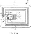
次に図4乃至図6により、本発明の第3の実施の形態について説明する。
図4乃至図6に示す実施の形態は、ICチップ12およびコンデンサ17の配置位置が異なるのみであり、他は図1乃至図3に示す第1の実施の形態と略同一である。
図4に示すように、アンテナ回路13の一方のアンテナ端子13aはICチップ12に接続され、またアンテナ回路13の他方のアンテナ端子13bは絶縁層14上に設けられた接続層15に接続されている。
またICチップ12は接続層15の一方の端部15aにICチップ接続端子13cを介して接続され、接続層15の他方の端部15bは他方のアンテナ端子13bに接続されている。
またコンデンサ17はアンテナ回路13の一方のアンテナ端子13aに第1連結層25を介して接続され、またコンデンサ17は接続層15の一方の端部15aにICチップ接続端子13cおよび第2連結層26を介して接続されている。
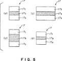
コンデンサ17は導電性インキにより、第2連結層26と一体に印刷された第1電極層17aと、絶縁性インキにより印刷された誘電層17bと、導電性インキにより第1連結層25と一体に印刷された第2電極層17cとを有している。
このように第1電極層17aと、誘電層17bと、第2電極層17cは各々インキにより形成されるので、各々の幅及び厚みを任意に定めることができる(図5(a)−(d))。すなわち、基準の幅および厚みを有するコンデンサ17(図5(a))に対して、その幅を2倍とすることによりコンデンサ17の容量が2倍となる(図5(b))。また誘電層17bの厚さを2倍とすることにより、コンデンサ17の容量が1/2となる(図5(c))。さらに誘電層17bの厚さを1/2とすることにより、コンデンサ17の容量が2倍となる(図5(d))。
図4において、アンテナ回路13のL=1.2μH、コンデンサ17のC=20pFとなっている。またICチップ12を実装したところ、共振周波数f=13.56MH2となった。
また、図6(a)−(e)に示すように、コンデンサ17の第1電極層17a、誘電層17bおよび第2電極層17cの平面上の配置位置を所望に対して任意に定めることができる。
第4の実施の形態
次に図7により本発明の第4の実施の形態について説明する。
図7(a)−(f)は、本発明によるICカードの第4の実施の形態を説明する図である。非接触ICカード30は、以下のように作製される。
(1)厚さ100μmのポリエチレンテレフタレートフィルムのカード基材31の上に、2μm厚の接着剤層31aをコーティングする(図7(a);接着剤コーティング工程)。
(2)(1)で接着剤層31aをコーティングしたカード基材31の上に、導電性インキにより、アンテナ回路33、ICチップ接続端子33c及びコンデンサ37の第1電極層37aをスクリーン印刷で形成して乾燥する(図7(b);第1導電印刷工程)。
(3)(2)で形成されたアンテナ回路33及び第1電極層37aの上に、絶縁性インキにより、絶縁層34及び誘電層37bをスクリーン印刷で形成して乾燥する(図7(c);絶縁印刷工程)。
(4)(3)で形成された絶縁層34及び誘電層37bの上に、導電性インキにより、接続層35および第2電極層37cをスクリーン印刷で形成して乾燥する(図7(d);第2導電印刷工程)。
(5)(4)で接続層35等を形成したカード基材31のアンテナ回路33及びICチップ接続端子33cの上に、異方性導電接着フィルム38を介してICチップ32を加熱圧着して実装する(図7(e);ICチップ実装工程)。
(6)(5)でICチップ32を実装したカード基材31に、厚さ250μmの熱接着シートによる第1保護層36aと、下面に接着剤23がコーティングされた厚さ100μmの第2保護層36bとを順次重ねて、加熱加圧ラミネートする(図7(f)保護層形成工程)。
(7)以上により、総厚0.45mmの非接触式ICカード30が完成する。
第5の実施の形態
次に図8により本発明の第5の実施の形態について説明する。
図8は、本発明による非接触ICカードの実施形態の製造方法を説明する図である。非接触ICカード40は、以下のように作製する。
(1)厚さ100μmのポリエチレンテレフタレートフィルムのカード基材41の両面に、2μm厚の接着剤層41aをコーティングする(図8(a);接着剤コーティング工程)。
(2)(1)で接着剤層41aをコーティングしたカード基材41の上面に、導電性インキにより、アンテナ回路43、ICチップ接続端子43c及びコンデンサ47の第1電極層47aをスクリーン印刷で形成して乾燥する(図8(b);第1導電印刷工程)。
(3)(2)で形成されたアンテナ回路43及び第1電極層47aの上に、絶縁性インキにより、絶縁層44及び誘電層47bをスクリーン印刷で形成して乾燥する(図8(c);絶縁印刷工程)。
(4)(3)で形成された絶縁層44及び誘電層47bの上に、導電性インキにより、接続層45および第2電極層47cをスクリーン印刷で形成して乾燥する(図8(d);第2導電印刷工程)。
(5)(4)で接続層45等を形成したカード基材41のアンテナ回路43及びICチップ接続端子43cの上に、異方性導電接着フィルム48を介してICチップ42を加熱圧着して実装する(図8(e);ICチップ実装工程)。
(6)(5)でICチップ42を実装したカード基材41に、両面に接着剤22がコーティングされICチップ42用の穿孔50が形成された厚さ250μmの第1保護層46aと、両面に接着剤23がコーティングされた厚さ100μmの第2保護層46bとを順次重ねる。さらにその下側から厚さ2μmの接着剤24がコーティングされた厚さ150μmの第1絵柄保護層47aと、上側から同じく接着剤25を有する第2絵柄保護層47bとを重ね合わせて、加熱加圧ラミネートする(図8(f)保護層形成工程)。
(7)以上により、総厚0.75mmの非接触式ICカード40が完成する。本実施の形態によれば、絵柄の印刷された絵柄層47a,47bを表裏に有し、基本構成をそのままにして絵柄の変更だけでカードを作成することが可能である。また、絵柄層47a,47bに、ICチツプ12内の情報を表示してもよい。
このことから生産性のよさに加え小ロット・多品目対応あるいはICカードの高機能化が可能である。Technical field
The present invention relates to a non-contact IC card that exchanges data with an external reader / writer in a non-contact manner and a method for manufacturing a non-contact IC card.
Background art
A conventional non-contact IC card has a winding coil wound with a thin conductive wire bonded to a card base, and an electronic component such as an IC chip or a capacitor is mounted, and then the card base is stored in a plastic case. In some cases, the card substrate is directly plated or etched to form a coil pattern antenna and an electronic component such as an IC chip or a capacitor is mounted, and then the card substrate is sandwiched between plastic sheets or the like.
However, the above-described conventional non-contact IC card having a wound coil lacks flexibility and has a large card thickness, so it is inferior in portability. The card thickness of the contact IC card is ISO standard 0.76 ± 0.08 mm, but most of the non-contact IC cards with winding coils exceed 1 mm. Also, the price is expensive.
A non-contact IC card of a pattern antenna by plating or etching is expensive because the manufacturing process is complicated.
In particular, when mounting a small IC chip, a jumper wire that straddles the antenna circuit is required to connect the antenna terminal and the IC chip, and the jumper wire is formed on the back surface of the card substrate to prevent a short circuit. Must. And since the jumper wire is connected to the antenna circuit on the surface by a through hole opened in the card base material, the manufacturing process is complicated. Further, the card substrate has to be sandwiched from both sides with a plastic sheet or the like, so the productivity is not good.
In addition, when the number of turns of the antenna coil is required to obtain communication characteristics, an antenna circuit is formed on both sides of the card substrate, or the antenna circuit end is overlapped with a through hole. It was necessary to connect, and the manufacturing process was complicated.
An object of the present invention is to provide a non-contact IC card that can be thinned and that is inexpensive, and a method of manufacturing the same.
Disclosure of the invention
The present invention provides a card base, an IC chip provided on one surface of the card base, and a card base on the same surface as the IC chip, and has a pair of antenna terminals, and one antenna terminal is an IC. An antenna circuit connected to the chip, an insulating layer provided so as to cover a part of the antenna circuit, a pair of end portions provided on the insulating layer, and one end portion connected to the IC chip, A connection layer connected to the other antenna terminal of the antenna circuit, an IC chip, an antenna circuit, a connection layer, and a protective layer that protects the connection layer. It is a non-contact IC card characterized by the above.
The present invention is a non-contact IC card, wherein the antenna circuit and the connection layer are formed by printing conductive ink, and the insulating layer is formed by insulating ink.
The present invention is a contactless IC card characterized in that a capacitor connected to the antenna circuit is provided on the same surface as the antenna circuit of the card substrate.
In the present invention, the capacitor is formed of a first electrode layer formed of conductive ink, a dielectric layer formed on the first electrode and formed of insulating ink, and a capacitor formed on the dielectric layer using conductive ink. A non-contact IC card comprising: a second electrode layer.
The present invention is a non-contact IC card characterized in that an additional antenna circuit is provided on the antenna circuit via an additional connection layer.
The present invention is the non-contact IC card, wherein the protective layer has a first protective layer disposed on the card substrate side and a second protective layer provided on the first protective layer.
The present invention is a non-contact IC card, wherein the first protective layer is provided with perforations through which an IC chip is passed.
The present invention is the non-contact IC card, wherein the first protective layer is made of a thermal adhesive sheet.
The present invention is a non-contact IC card characterized in that a pattern layer is provided on each of a card base and a protective layer.
The present invention is the non-contact IC card, wherein the capacitor is arranged to be connected to one antenna terminal of the antenna circuit and one end of the connection layer.
According to the present invention, the capacitor is connected to one antenna terminal of the antenna circuit via the first connection layer, and is connected to one end of the connection layer via the second connection layer. IC card.
In the present invention, the antenna circuit and the capacitor first electrode layer are disposed on the same plane, the insulating layer and the capacitor dielectric layer are disposed on the same plane, and the connection layer and the capacitor second electrode layer are disposed on the same plane. It is a non-contact IC card characterized by being arranged.
The present invention has a card substrate and an IC chip, an antenna circuit, and a capacitor provided on the card substrate, and connects the IC chip and the antenna circuit via a connection layer provided on an insulating layer. In the method for manufacturing a non-contact IC card, a first conductive printing step for printing an antenna circuit and a first electrode layer at a predetermined position on one surface of a card base, and an antenna circuit formed by the first conductive printing step An insulating layer printed on the first electrode layer formed in the first conductive printing step, and an insulating layer printed in the insulating printing step. And a second conductive printing step of printing a connection layer on the dielectric layer printed in the insulating printing step to form a capacitor by printing a second electrode layer. IC car It is a method of manufacture.
The present invention further comprises a step of providing an IC chip, an antenna circuit, an insulating layer, and a protective layer for protecting the connection layer on the card substrate. It is.
[Brief description of the drawings]
FIG. 1 is a perspective view showing the configuration of a first embodiment of a non-contact IC card according to the present invention.
FIG. 2 is a cross-sectional view showing details of the anisotropic conductive adhesive film used in the present embodiment.
FIG. 3 is a diagram for explaining a method of manufacturing an embodiment of a non-contact IC card according to the present invention.
FIG. 4 is a diagram showing a third embodiment of the non-contact IC card according to the present invention.
FIG. 5 is a side sectional view showing a capacitor of a non-contact IC card according to the present invention.
FIG. 6 is a plan view showing a capacitor of a non-contact IC card according to the present invention.
FIG. 7 is a view showing a fourth embodiment of the non-contact IC card according to the present invention.
FIG. 8 is a diagram showing a fifth embodiment of the non-contact IC card according to the present invention.
BEST MODE FOR CARRYING OUT THE INVENTION
First embodiment
Hereinafter, embodiments of the present invention will be described in more detail with reference to the drawings.
FIG. 1 is a perspective view showing a configuration of an embodiment of a contactless IC card according to the present invention.
The
The
The
The
The anisotropic conductive
Details will be described later.
The
The
The
In addition to the above, the resin binder (or ink vehicle) includes butyral resin, vinyl chloride / vinyl acetate copolymer resin, urethane resin, polyester resin, cellulose resin, acrylic resin, styrene / maleic acid copolymer resin. An epoxy resin or the like, and a rubber-based resin such as nitrile rubber or a urethane elastomer added as necessary can also be used. In consideration of heat resistance, a resin having a high glass transition temperature (Tg) such as polyamide, polyimide, polyethersulfone, or a system in which Tg is increased by a curing reaction can also be used. A surfactant, silane coupling agent, plasticizer, wax, silicone oil, etc. may be added to the above resin or ink vehicle as necessary.
In addition to the silver paste, the conductive ink can also be a paste containing copper powder or carbon filler in a binder resin similar to the above, or a paste obtained by mixing silver powder or copper powder with a carbon filler. .
The antenna terminal 13 a of the
Thus, the
The insulating
In addition to the above, the insulating
The
The
The first
The second
The
The
FIG. 2 is a cross-sectional view showing details of the anisotropic conductive
The anisotropic conductive
As shown in FIG. 2, when the
Next, a method for manufacturing a non-contact IC card will be described.
FIG. 3 is a diagram for explaining a method of manufacturing an embodiment of a contactless IC card according to the present invention.
The
(1) An adhesive layer 11a having a thickness of 25 μm is coated on a
(2) On the
(3) On the
(4) On the insulating
(5) The
(6) The
(7) As described above, the
According to the present embodiment, the
As described above in detail, according to the present invention, the antenna circuit includes the insulating layer formed on at least a part of the antenna circuit and the connection layer formed across the insulating layer. It can be formed only on the surface.
According to the invention, the antenna circuit, the connection layer, and the insulating layer are formed by printing, so that they are thin and inexpensive.
Further, according to the present invention, since the capacitor is provided, the received radio wave can be tuned.
According to the present invention, the capacitor is formed by printing the first electrode layer formed by printing the conductive ink, the dielectric layer formed by printing the insulating ink, and the conductive ink. Since it is provided with the formed second electrode layer, it is thin and inexpensive.
According to the invention, the first conductive printing step for printing the antenna circuit and the first electrode layer, the insulating printing step for printing the insulating layer and the dielectric layer, and the second conductive printing for printing the connection layer and the second electrode layer. A thin non-contact IC card can be manufactured at low cost.
Second embodiment
The present invention is not limited to the embodiment described above, and various modifications and changes are possible, and these are also within the equivalent scope of the present invention.
For example, when the number of turns of the
In that case, the additional insulating
In this way, the necessary number of antenna coil turns can be easily obtained without using through-holes by alternately printing conductive ink and insulating ink in a predetermined pattern.
Further, the protective layer may be only one layer. By doing so, it can be manufactured at a lower cost.
In that case, for example, a concave portion can be formed in the first
Third embodiment
Next, a third embodiment of the present invention will be described with reference to FIGS.
The embodiment shown in FIGS. 4 to 6 is substantially the same as the first embodiment shown in FIGS. 1 to 3 except that the arrangement positions of the
As shown in FIG. 4, one antenna terminal 13 a of the
The
The
The
Since the
In FIG. 4, L of the
Further, as shown in FIGS. 6A to 6E, the arrangement positions on the plane of the
Fourth embodiment
Next, a fourth embodiment of the present invention will be described with reference to FIG.
FIGS. 7A to 7F are diagrams for explaining a fourth embodiment of the IC card according to the present invention. The
(1) A 2 μm-
(2) On the
(3) On the
(4) On the insulating
(5) The
(6) The
(7) As described above, the non-contact
Fifth embodiment
Next, a fifth embodiment of the present invention will be described with reference to FIG.
FIG. 8 is a diagram for explaining a method of manufacturing an embodiment of a contactless IC card according to the present invention. The
(1) An adhesive layer 41a having a thickness of 2 μm is coated on both surfaces of a
(2) The
(3) On the
(4) On the insulating
(5) The
(6) A first protective layer 46a having a thickness of 250 μm in which the adhesive 22 is coated on both sides of the
(7) As described above, the non-contact
From this, in addition to good productivity, it is possible to handle small lots and multiple items, or to increase the functionality of IC cards.
Claims (9)
Translated fromJapaneseカード基材の一面に設けられたICチップと、
カード基材のICチップと同一面上に設けられ、一対のアンテナ端子を有するとともに、一方のアンテナ端子がICチップに接続されたアンテナ回路と、
アンテナ回路の一部分を覆って設けられた絶縁層と、
絶縁層上に設けられ、一対の端部を有するとともに、一方の端部がICチップに接続され、他方の端部がアンテナ回路の他方のアンテナ端子に接続された接続層と、
カード基材上に設けられ、ICチップと、アンテナ回路と接続層と、接続層を保護する保護層と、
を備え、
アンテナ回路と接続層は導電性インキを印刷することにより形成され、絶縁層は絶縁性インキにより形成され、
カード基材のアンテナ回路と同一面上に、アンテナ回路に接続されたコンデンサを設け、
コンデンサは導電性インキにより形成された第1電極層と、第1電極上に設けられ絶縁性インキにより形成された誘電層と、誘電層上に設けられ導電性インキにより形成された第2電極層と、を有し、
保護層はカード基材側に配置された第1保護層と、第1保護層上に設けられた第2保護層とを有し、
第1保護層に、ICチップを通させる穿孔が設けられていることを特徴とする非接触ICカード。A card substrate;
An IC chip provided on one surface of the card substrate;
An antenna circuit that is provided on the same surface as the IC chip of the card substrate, has a pair of antenna terminals, and one antenna terminal is connected to the IC chip;
An insulating layer provided to cover a part of the antenna circuit;
A connection layer provided on the insulating layer, having a pair of ends, one end connected to the IC chip, and the other end connected to the other antenna terminal of the antenna circuit;
An IC chip, an antenna circuit, a connection layer, a protective layer for protecting the connection layer, provided on the card substrate;
Equipped witha,
The antenna circuit and the connection layer are formed by printing conductive ink, the insulating layer is formed by insulating ink,
A capacitor connected to the antenna circuit is provided on the same surface as the antenna circuit of the card base,
The capacitor has a first electrode layer formed of conductive ink, a dielectric layer formed on the first electrode and formed of insulating ink, and a second electrode layer formed on the dielectric layer and formed of conductive ink. And having
The protective layer has a first protective layer disposed on the card substrate side, and a second protective layer provided on the first protective layer,
A non-contact IC card, wherein the first protective layer is provided with perforations that allow the IC chip to pass therethrough.
カード基材の一方の面の所定位置に、アンテナ回路及び第1電極層を導電性インキにより印刷する第1導電印刷工程と、
前記第1導電印刷工程で形成されたアンテナ回路の少なくとも一部分上に、絶縁層を絶縁性インキにより印刷するとともに、同時に前記第1導電印刷工程で形成された第1電極層上に、誘電層を絶縁性インキにより印刷する絶縁印刷工程と、
前記絶縁印刷工程で印刷された絶縁層上に接続層を導電性インキにより印刷するとともに、同時に前記絶縁印刷工程で印刷された誘電層上に、導電性インキにより第2電極層を印刷してコンデンサを形成する第2導電印刷工程と、
を備えたことを特徴とする非接触ICカードの製造方法。A non-contact IC card having a card substrate and an IC chip, an antenna circuit, and a capacitor provided on the card substrate, and connecting the IC chip and the antenna circuit via a connection layer provided on an insulating layer In the manufacturing method of
A first conductive printing stepof printing the antenna circuit and the first electrode layer with aconductive ink at a predetermined position on one surface of the card substrate;
An insulating layer is printed with aninsulating ink on at least a part of the antenna circuit formed in the first conductive printing process, and a dielectric layer is simultaneously formed on the first electrode layer formed in the first conductive printing process. An insulating printing process for printing with insulating ink;
The connection layer is printed with aconductive ink on the insulating layer printed in the insulating printing step, andat the same time , the second electrode layer is printed with theconductive ink on the dielectric layer printed in the insulating printing step. Forming a second conductive printing step;
A method of manufacturing a non-contact IC card, comprising:
Applications Claiming Priority (2)
| Application Number | Priority Date | Filing Date | Title |
|---|---|---|---|
| JP19256498 | 1998-07-08 | ||
| PCT/JP1999/003709WO2000003354A1 (en) | 1998-07-08 | 1999-07-08 | Noncontact ic card and manufacture thereof |
Publications (1)
| Publication Number | Publication Date |
|---|---|
| JP4187278B2true JP4187278B2 (en) | 2008-11-26 |
Family
ID=16293391
Family Applications (1)
| Application Number | Title | Priority Date | Filing Date |
|---|---|---|---|
| JP56298399AExpired - Fee RelatedJP4187278B2 (en) | 1998-07-08 | 1999-07-08 | Non-contact IC card and manufacturing method thereof |
Country Status (5)
| Country | Link |
|---|---|
| US (1) | US6459588B1 (en) |
| EP (1) | EP1014302B1 (en) |
| JP (1) | JP4187278B2 (en) |
| DE (1) | DE69927342T2 (en) |
| WO (1) | WO2000003354A1 (en) |
Families Citing this family (93)
| Publication number | Priority date | Publication date | Assignee | Title |
|---|---|---|---|---|
| JP3828581B2 (en)* | 1996-12-26 | 2006-10-04 | 株式会社日立製作所 | Semiconductor device and manufacturing method thereof |
| KR100629923B1 (en)* | 1998-09-30 | 2006-09-29 | 돗빤호무즈가부시기가이샤 | Conductive paste, curing method therof, method for fabricating antenna for contactless data transmitter-receiver, and contactless data transmitter-receiver |
| US6468638B2 (en) | 1999-03-16 | 2002-10-22 | Alien Technology Corporation | Web process interconnect in electronic assemblies |
| DE19939347C1 (en)* | 1999-08-19 | 2001-02-15 | Orga Kartensysteme Gmbh | Chip card manufacture, of e.g. credit cards or admission cards, which allows for fitting with displays or keys, involves laminating circuit board with several perforated layers and machining cut-outs |
| WO2001061644A1 (en)* | 2000-02-14 | 2001-08-23 | Koninklijke Philips Electronics N.V. | Transponder and appliance |
| KR100732648B1 (en)* | 2000-02-22 | 2007-06-28 | 도레이엔지니어링가부시키가이샤 | Contactless ID card and its manufacturing method |
| WO2001073685A1 (en)* | 2000-03-28 | 2001-10-04 | Lucatron Ag | Rfid label with an element for regulating the resonance frequency |
| FI112287B (en) | 2000-03-31 | 2003-11-14 | Rafsec Oy | Procedure for producing product sensor and product sensor |
| DE60102577T2 (en)* | 2000-04-18 | 2005-02-03 | Nagraid S.A. | ELECTRONIC LABEL |
| JP2002074300A (en)* | 2000-08-31 | 2002-03-15 | Shinko Electric Ind Co Ltd | Non-contact type IC card and method of manufacturing the same |
| US6628240B2 (en)* | 2000-11-08 | 2003-09-30 | American Pacific Technology | Method and apparatus for rapid staking of antennae in smart card manufacture |
| FI113851B (en)* | 2000-11-20 | 2004-06-30 | Rafsec Oy | Method of attaching a chip's integrated circuit to an intelligent self-adhesive label and method of pre-treating a silicon wafer |
| DE10058804C2 (en)* | 2000-11-27 | 2002-11-28 | Smart Pac Gmbh Technology Serv | Chip module and chip card module for producing a chip card |
| FI112121B (en) | 2000-12-11 | 2003-10-31 | Rafsec Oy | Smart label web, process for making the same, method for making a carrier web and construction part for a smart label in a smart label web |
| JP2002230498A (en)* | 2001-01-31 | 2002-08-16 | Toppan Forms Co Ltd | IC chip mounting method |
| JP4565595B2 (en)* | 2001-02-16 | 2010-10-20 | トッパン・フォームズ株式会社 | Non-contact type antenna for data transceiver and its capacitance adjustment method |
| JP2004520722A (en)* | 2001-05-17 | 2004-07-08 | コーニンクレッカ フィリップス エレクトロニクス エヌ ヴィ | Article having a substrate and a chip attached to the substrate |
| FR2825228B1 (en) | 2001-05-25 | 2003-09-19 | Framatome Connectors Int | METHOD FOR MANUFACTURING A PRINTED CIRCUIT AND PLANAR ANTENNA MANUFACTURED THEREWITH |
| US6606247B2 (en)* | 2001-05-31 | 2003-08-12 | Alien Technology Corporation | Multi-feature-size electronic structures |
| FI112550B (en) | 2001-05-31 | 2003-12-15 | Rafsec Oy | Smart label and smart label path |
| JP2002366916A (en)* | 2001-06-06 | 2002-12-20 | Lintec Corp | Composite tag and manufacture thereof |
| CN1283371C (en)* | 2001-06-19 | 2006-11-08 | 奥尔约恩有限责任公司 | UV curable inks for PTF lamination (including flex circuits) |
| JP2003012020A (en)* | 2001-06-28 | 2003-01-15 | Toppan Printing Co Ltd | Binding band with IC tag |
| FI117331B (en) | 2001-07-04 | 2006-09-15 | Rafsec Oy | Method of manufacturing an injection molded product |
| US6693541B2 (en)* | 2001-07-19 | 2004-02-17 | 3M Innovative Properties Co | RFID tag with bridge circuit assembly and methods of use |
| US6701605B2 (en) | 2001-10-09 | 2004-03-09 | Sonoco Development, Inc. | Conductive electrical element and antenna with ink additive technology |
| FI119401B (en) | 2001-12-21 | 2008-10-31 | Upm Raflatac Oy | Smart label web and process for its manufacture |
| US7214569B2 (en) | 2002-01-23 | 2007-05-08 | Alien Technology Corporation | Apparatus incorporating small-feature-size and large-feature-size components and method for making same |
| US20030151028A1 (en)* | 2002-02-14 | 2003-08-14 | Lawrence Daniel P. | Conductive flexographic and gravure ink |
| FR2841089B1 (en)* | 2002-06-14 | 2004-07-30 | Sequoias | METHOD OF INDUSTRIAL MANUFACTURE OF ANTENNAS FOR RFID TRANSPONDERS |
| FR2842950B1 (en)* | 2002-07-25 | 2004-10-22 | Framatome Connectors Int | CAPACITIVE ANTENNA AND PRODUCTION METHOD |
| FR2844621A1 (en)* | 2002-09-13 | 2004-03-19 | A S K | Method for manufacturing without contact or hybrid integrated circuit card, comprises application of two thermoplastic layers under temperature and pressure followed by two hot pressed plastic layers |
| US7140712B2 (en)* | 2002-10-22 | 2006-11-28 | Seiko Epson Corporation | Liquid cartridge |
| CN1706040A (en)* | 2002-10-24 | 2005-12-07 | 东丽工程株式会社 | Non-contact ID card and the like and its manufacturing method |
| JP2004177989A (en)* | 2002-11-22 | 2004-06-24 | Sony Corp | Noncontact ic card |
| US6861993B2 (en)* | 2002-11-25 | 2005-03-01 | 3M Innovative Properties Company | Multi-loop antenna for radio-frequency identification |
| US7102522B2 (en)* | 2002-12-24 | 2006-09-05 | 3M Innovative Properties Company | Tamper-indicating radio frequency identification antenna and sticker, a radio frequency identification antenna, and methods of using the same |
| US6816125B2 (en)* | 2003-03-01 | 2004-11-09 | 3M Innovative Properties Company | Forming electromagnetic communication circuit components using densified metal powder |
| US7253735B2 (en) | 2003-03-24 | 2007-08-07 | Alien Technology Corporation | RFID tags and processes for producing RFID tags |
| FR2853115B1 (en)* | 2003-03-28 | 2005-05-06 | A S K | METHOD FOR MANUFACTURING A CHIP CARD ANTENNA ON A THERMOPLASTIC CARRIER AND A CHIP CARD OBTAINED BY SAID METHOD |
| FR2855637B1 (en)* | 2003-05-26 | 2005-11-18 | A S K | METHOD FOR MANUFACTURING CONTACTLESS TICKET AND TICKET OBTAINED THEREBY |
| JP2005078442A (en)* | 2003-09-01 | 2005-03-24 | Sony Corp | Ic card, and its manufacturing method |
| US7004060B2 (en)* | 2003-11-04 | 2006-02-28 | Industrial Technology Research Institute | Balancing vertical load device for a motor |
| US20050101843A1 (en)* | 2003-11-06 | 2005-05-12 | Welch Allyn, Inc. | Wireless disposable physiological sensor |
| FR2863389B1 (en)* | 2003-12-04 | 2006-06-02 | Francois Charles Oberthur Fidu | SAFETY DOCUMENT HAVING INVARIABLE AND VARIABLE PRINTED CHARACTERISTICS AND METHOD OF MANUFACTURE |
| US6999028B2 (en)* | 2003-12-23 | 2006-02-14 | 3M Innovative Properties Company | Ultra high frequency radio frequency identification tag |
| US7633145B2 (en)* | 2004-01-16 | 2009-12-15 | Semiconductor Energy Laboratory Co., Ltd. | Semiconductor device with antenna and separating layer |
| CN1910600B (en)* | 2004-01-23 | 2011-12-14 | 株式会社半导体能源研究所 | ID label, ID card, and ID tag |
| US20090065586A1 (en)* | 2004-02-06 | 2009-03-12 | Kouji Tasaki | Electronic device |
| US7417599B2 (en)* | 2004-02-20 | 2008-08-26 | 3M Innovative Properties Company | Multi-loop antenna for radio frequency identification (RFID) communication |
| US7268687B2 (en)* | 2004-03-23 | 2007-09-11 | 3M Innovative Properties Company | Radio frequency identification tags with compensating elements |
| KR100602621B1 (en)* | 2004-06-16 | 2006-07-19 | 한국조폐공사 | Prefabricated combi card and its manufacturing method |
| US7551141B1 (en) | 2004-11-08 | 2009-06-23 | Alien Technology Corporation | RFID strap capacitively coupled and method of making same |
| US7452748B1 (en) | 2004-11-08 | 2008-11-18 | Alien Technology Corporation | Strap assembly comprising functional block deposited therein and method of making same |
| US7688206B2 (en) | 2004-11-22 | 2010-03-30 | Alien Technology Corporation | Radio frequency identification (RFID) tag for an item having a conductive layer included or attached |
| US7385284B2 (en) | 2004-11-22 | 2008-06-10 | Alien Technology Corporation | Transponder incorporated into an electronic device |
| DE102005002733B4 (en)* | 2005-01-20 | 2016-05-12 | Giesecke & Devrient Gmbh | Portable data carrier |
| US20090032602A1 (en)* | 2005-04-28 | 2009-02-05 | Toyo Boseki Kabushiki Kaisha | Thermobondable polyester film, process for production of ic cards or ic tags with the same, and ic cards with ic tags |
| US7542301B1 (en) | 2005-06-22 | 2009-06-02 | Alien Technology Corporation | Creating recessed regions in a substrate and assemblies having such recessed regions |
| TWI339358B (en)* | 2005-07-04 | 2011-03-21 | Hitachi Ltd | Rfid tag and manufacturing method thereof |
| US7432816B1 (en)* | 2005-10-13 | 2008-10-07 | Hewlett-Packard Development Company, L.P. | Printed circuit board with RFID antenna |
| US7183924B1 (en) | 2005-10-13 | 2007-02-27 | Hewlett-Packard Development Company, L.P. | Storing configuration information and a service record for an item in an RFID tag |
| US7646305B2 (en)* | 2005-10-25 | 2010-01-12 | Checkpoint Systems, Inc. | Capacitor strap |
| US20070218258A1 (en)* | 2006-03-20 | 2007-09-20 | 3M Innovative Properties Company | Articles and methods including patterned substrates formed from densified, adhered metal powders |
| EP2013821B1 (en)* | 2006-04-10 | 2011-10-12 | Innovatier, Inc. | An electronic inlay module for electronic cards and tags, electronic card and methods for manufacturing such electronic inlay modules and cards |
| US7646304B2 (en)* | 2006-04-10 | 2010-01-12 | Checkpoint Systems, Inc. | Transfer tape strap process |
| US20080055045A1 (en)* | 2006-08-31 | 2008-03-06 | 3M Innovative Properties Company | Rfid tag including a three-dimensional antenna |
| US20080143519A1 (en)* | 2006-12-19 | 2008-06-19 | 3M Innovative Properties Company | Tamper-indicating radio frequency identification tag and methods of indicating tampering of a radio frequency identification tag |
| DE102007028357A1 (en) | 2007-06-15 | 2008-12-24 | Ksw Microtec Ag | transponder card |
| DE102007041751B4 (en)* | 2007-09-04 | 2018-04-19 | Bielomatik Leuze Gmbh + Co. Kg | Method and device for producing an RFID tag |
| US20090085750A1 (en)* | 2007-09-27 | 2009-04-02 | 3M Innovative Properties Company | Extended RFID tag |
| US8289163B2 (en)* | 2007-09-27 | 2012-10-16 | 3M Innovative Properties Company | Signal line structure for a radio-frequency identification system |
| US8717244B2 (en)* | 2007-10-11 | 2014-05-06 | 3M Innovative Properties Company | RFID tag with a modified dipole antenna |
| US7946502B2 (en)* | 2008-01-22 | 2011-05-24 | Visa Usa Inc. | Financial transaction token |
| US7982616B2 (en)* | 2008-02-14 | 2011-07-19 | 3M Innovative Properties Company | Radio frequency identification (RFID) tag including a three-dimensional loop antenna |
| JP5047862B2 (en)* | 2008-03-31 | 2012-10-10 | 三菱自動車工業株式会社 | Panel device |
| WO2009140658A1 (en)* | 2008-05-15 | 2009-11-19 | Kovio, Inc. | Surveillance devices with multiple capacitors |
| KR101148534B1 (en)* | 2008-05-28 | 2012-05-21 | 가부시키가이샤 무라타 세이사쿠쇼 | Wireless ic device and component for a wireless ic device |
| EP2286445A1 (en) | 2008-06-02 | 2011-02-23 | Nxp B.V. | Method for manufacturing an electronic device |
| KR101079360B1 (en)* | 2009-08-19 | 2011-11-02 | 삼성전기주식회사 | Radio Frequency Identification Tag, Method and Mould for Manufacturing the same |
| KR101079543B1 (en)* | 2009-08-19 | 2011-11-02 | 삼성전기주식회사 | Radio Frequency Identification Tag, Method and Mould for Manufacturing the same |
| DE102009058435A1 (en)* | 2009-12-16 | 2011-06-22 | Giesecke & Devrient GmbH, 81677 | Attaching and electrically connecting a chip module to a chip card |
| JP5501114B2 (en)* | 2010-06-25 | 2014-05-21 | 東洋アルミニウム株式会社 | Antenna circuit assembly for IC card / tag and manufacturing method thereof |
| US8912890B2 (en) | 2012-10-01 | 2014-12-16 | Thin Film Electronics Asa | Surveillance devices with multiple capacitors |
| US8847349B2 (en)* | 2012-12-21 | 2014-09-30 | Texas Instruments Incorporated | Integrated circuit package with printed circuit layer |
| RU2664719C2 (en) | 2013-11-01 | 2018-08-23 | Ппг Индастриз Огайо, Инк. | Methods of transferring electrically conductive materials |
| CA2901026C (en)* | 2014-08-19 | 2020-11-24 | Western Michigan University Research Foundation | Helmet impact monitoring system |
| TWI651830B (en)* | 2015-02-17 | 2019-02-21 | 立昌先進科技股份有限公司 | Multifunctinal miniaturized smd electronic components and process for manufacturing the same |
| ES2670649T3 (en)* | 2015-03-02 | 2018-05-31 | Gemalto Sa | Manufacturing procedure of a radio frequency device with passive wired antenna |
| JP6274135B2 (en)* | 2015-03-12 | 2018-02-07 | 株式会社村田製作所 | Coil module |
| FR3040516B1 (en)* | 2015-08-27 | 2017-09-15 | Linxens Holding | METHOD FOR MANUFACTURING AN ELECTRIC CIRCUIT, ELECTRIC CIRCUIT OBTAINED BY THIS METHOD AND CHIP CARD COMPRISING SUCH AN ELECTRICAL CIRCUIT |
| EP3182507A1 (en)* | 2015-12-15 | 2017-06-21 | Gemalto Sa | Single-sided antenna module with smd component |
| CA3083837A1 (en) | 2019-06-12 | 2020-12-12 | The Board Of Trustees Of Western Michigan University | Pressure monitoring system for helmets |
Family Cites Families (12)
| Publication number | Priority date | Publication date | Assignee | Title |
|---|---|---|---|---|
| ZA941671B (en)* | 1993-03-11 | 1994-10-12 | Csir | Attaching an electronic circuit to a substrate. |
| US5541399A (en)* | 1994-09-30 | 1996-07-30 | Palomar Technologies Corporation | RF transponder with resonant crossover antenna coil |
| JP3064840B2 (en)* | 1994-12-22 | 2000-07-12 | ソニー株式会社 | IC card |
| US5952713A (en)* | 1994-12-27 | 1999-09-14 | Takahira; Kenichi | Non-contact type IC card |
| JPH08216570A (en) | 1995-02-09 | 1996-08-27 | Hitachi Chem Co Ltd | Ic card |
| FR2747866B1 (en)* | 1996-04-22 | 1998-06-19 | Em Microelectronic Marin Sa | ELECTRONIC ASSEMBLY INCLUDING AN ELECTRONIC UNIT CONNECTED TO A COIL |
| US5892661A (en) | 1996-10-31 | 1999-04-06 | Motorola, Inc. | Smartcard and method of making |
| JPH10193851A (en) | 1997-01-08 | 1998-07-28 | Denso Corp | Non-contact card |
| JP3350405B2 (en)* | 1997-07-28 | 2002-11-25 | 株式会社日立製作所 | Semiconductor device |
| JPH1185937A (en)* | 1997-09-02 | 1999-03-30 | Nippon Lsi Card Kk | Non-contact lsi card and method for inspecting the same |
| JP3767654B2 (en) | 1997-09-19 | 2006-04-19 | セイコーエプソン株式会社 | Radio wave response sheet and manufacturing method thereof |
| JPH11250214A (en)* | 1998-03-03 | 1999-09-17 | Matsushita Electron Corp | Component mounting method, IC card and method of manufacturing the same |
- 1999
- 1999-07-08USUS09/508,064patent/US6459588B1/ennot_activeExpired - Fee Related
- 1999-07-08WOPCT/JP1999/003709patent/WO2000003354A1/enactiveIP Right Grant
- 1999-07-08DEDE69927342Tpatent/DE69927342T2/ennot_activeExpired - Lifetime
- 1999-07-08EPEP99929764Apatent/EP1014302B1/ennot_activeExpired - Lifetime
- 1999-07-08JPJP56298399Apatent/JP4187278B2/ennot_activeExpired - Fee Related
Also Published As
| Publication number | Publication date |
|---|---|
| EP1014302A1 (en) | 2000-06-28 |
| DE69927342T2 (en) | 2006-06-22 |
| DE69927342D1 (en) | 2005-10-27 |
| US6459588B1 (en) | 2002-10-01 |
| EP1014302A4 (en) | 2001-05-16 |
| WO2000003354A1 (en) | 2000-01-20 |
| EP1014302B1 (en) | 2005-09-21 |
Similar Documents
| Publication | Publication Date | Title |
|---|---|---|
| JP4187278B2 (en) | Non-contact IC card and manufacturing method thereof | |
| EP2192530B1 (en) | Antenna sheet, transponder and booklet | |
| EP1739598B1 (en) | Antenna circuit, IC inlet, IC tag and IC card, as well as manufacturing method of IC card | |
| JP4860436B2 (en) | IC card and manufacturing method thereof | |
| JP5287731B2 (en) | Transponder and booklet | |
| JP2001010264A (en) | Non-contact type IC card and its antenna characteristic adjusting method | |
| JP2003317060A (en) | IC card | |
| WO2001001342A1 (en) | Ic card | |
| JP2004054337A (en) | IC chip package | |
| JP2000235635A (en) | Non-contact IC card with built-in capacitor and method of manufacturing the same | |
| JP4176244B2 (en) | Chip card | |
| JP3953775B2 (en) | Multi-contact substrate for non-contact data carrier and multi-contact non-contact data carrier | |
| JP2000036020A (en) | Non-contact IC card | |
| JP2017227959A (en) | Non-contact information medium and method for manufacturing non-contact information medium | |
| JP4693295B2 (en) | Circuit formation method | |
| JPH11175676A (en) | Non-contact IC card | |
| JP4343297B2 (en) | IC card substrate and manufacturing method thereof | |
| JP2002304613A (en) | Non-contact type IC card and method of manufacturing the same | |
| JP4281102B2 (en) | IC card | |
| JP4777015B2 (en) | Communication circuit holder | |
| US20070012773A1 (en) | Method of making an electronic device using an electrically conductive polymer, and associated products | |
| JP4139488B2 (en) | Non-contact IC card | |
| JP2002183696A (en) | Method of manufacturing coil of ic card | |
| JP2002197433A (en) | IC card and manufacturing method thereof | |
| JP2001229356A (en) | Non-contact IC card antenna and non-contact IC card |
Legal Events
| Date | Code | Title | Description |
|---|---|---|---|
| A621 | Written request for application examination | Free format text:JAPANESE INTERMEDIATE CODE: A621 Effective date:20060628 | |
| A131 | Notification of reasons for refusal | Free format text:JAPANESE INTERMEDIATE CODE: A131 Effective date:20080513 | |
| A521 | Request for written amendment filed | Free format text:JAPANESE INTERMEDIATE CODE: A523 Effective date:20080714 | |
| TRDD | Decision of grant or rejection written | ||
| A01 | Written decision to grant a patent or to grant a registration (utility model) | Free format text:JAPANESE INTERMEDIATE CODE: A01 Effective date:20080902 | |
| A01 | Written decision to grant a patent or to grant a registration (utility model) | Free format text:JAPANESE INTERMEDIATE CODE: A01 | |
| A61 | First payment of annual fees (during grant procedure) | Free format text:JAPANESE INTERMEDIATE CODE: A61 Effective date:20080909 | |
| R150 | Certificate of patent or registration of utility model | Free format text:JAPANESE INTERMEDIATE CODE: R150 | |
| FPAY | Renewal fee payment (event date is renewal date of database) | Free format text:PAYMENT UNTIL: 20110919 Year of fee payment:3 | |
| FPAY | Renewal fee payment (event date is renewal date of database) | Free format text:PAYMENT UNTIL: 20110919 Year of fee payment:3 | |
| FPAY | Renewal fee payment (event date is renewal date of database) | Free format text:PAYMENT UNTIL: 20120919 Year of fee payment:4 | |
| FPAY | Renewal fee payment (event date is renewal date of database) | Free format text:PAYMENT UNTIL: 20120919 Year of fee payment:4 | |
| FPAY | Renewal fee payment (event date is renewal date of database) | Free format text:PAYMENT UNTIL: 20130919 Year of fee payment:5 | |
| LAPS | Cancellation because of no payment of annual fees |