JP4186536B2 - Plasma processing equipment - Google Patents
Plasma processing equipmentDownload PDFInfo
- Publication number
- JP4186536B2 JP4186536B2JP2002209052AJP2002209052AJP4186536B2JP 4186536 B2JP4186536 B2JP 4186536B2JP 2002209052 AJP2002209052 AJP 2002209052AJP 2002209052 AJP2002209052 AJP 2002209052AJP 4186536 B2JP4186536 B2JP 4186536B2
- Authority
- JP
- Japan
- Prior art keywords
- electrode
- plasma
- plasma processing
- silicon wafer
- semiconductor substrate
- Prior art date
- Legal status (The legal status is an assumption and is not a legal conclusion. Google has not performed a legal analysis and makes no representation as to the accuracy of the status listed.)
- Expired - Fee Related
Links
Images


Classifications
- H—ELECTRICITY
- H01—ELECTRIC ELEMENTS
- H01L—SEMICONDUCTOR DEVICES NOT COVERED BY CLASS H10
- H01L21/00—Processes or apparatus adapted for the manufacture or treatment of semiconductor or solid state devices or of parts thereof
- H01L21/02—Manufacture or treatment of semiconductor devices or of parts thereof
- H01L21/04—Manufacture or treatment of semiconductor devices or of parts thereof the devices having potential barriers, e.g. a PN junction, depletion layer or carrier concentration layer
- H01L21/18—Manufacture or treatment of semiconductor devices or of parts thereof the devices having potential barriers, e.g. a PN junction, depletion layer or carrier concentration layer the devices having semiconductor bodies comprising elements of Group IV of the Periodic Table or AIIIBV compounds with or without impurities, e.g. doping materials
- H01L21/30—Treatment of semiconductor bodies using processes or apparatus not provided for in groups H01L21/20 - H01L21/26
- H01L21/302—Treatment of semiconductor bodies using processes or apparatus not provided for in groups H01L21/20 - H01L21/26 to change their surface-physical characteristics or shape, e.g. etching, polishing, cutting
- H01L21/306—Chemical or electrical treatment, e.g. electrolytic etching
- H01L21/3065—Plasma etching; Reactive-ion etching
- H—ELECTRICITY
- H01—ELECTRIC ELEMENTS
- H01L—SEMICONDUCTOR DEVICES NOT COVERED BY CLASS H10
- H01L21/00—Processes or apparatus adapted for the manufacture or treatment of semiconductor or solid state devices or of parts thereof
- H01L21/67—Apparatus specially adapted for handling semiconductor or electric solid state devices during manufacture or treatment thereof; Apparatus specially adapted for handling wafers during manufacture or treatment of semiconductor or electric solid state devices or components ; Apparatus not specifically provided for elsewhere
- H01L21/67005—Apparatus not specifically provided for elsewhere
- H01L21/67011—Apparatus for manufacture or treatment
- H01L21/67098—Apparatus for thermal treatment
- H01L21/67109—Apparatus for thermal treatment mainly by convection
- H—ELECTRICITY
- H01—ELECTRIC ELEMENTS
- H01J—ELECTRIC DISCHARGE TUBES OR DISCHARGE LAMPS
- H01J37/00—Discharge tubes with provision for introducing objects or material to be exposed to the discharge, e.g. for the purpose of examination or processing thereof
- H01J37/02—Details
- H01J37/20—Means for supporting or positioning the object or the material; Means for adjusting diaphragms or lenses associated with the support
- H—ELECTRICITY
- H01—ELECTRIC ELEMENTS
- H01J—ELECTRIC DISCHARGE TUBES OR DISCHARGE LAMPS
- H01J37/00—Discharge tubes with provision for introducing objects or material to be exposed to the discharge, e.g. for the purpose of examination or processing thereof
- H01J37/32—Gas-filled discharge tubes
- H01J37/32431—Constructional details of the reactor
- H—ELECTRICITY
- H01—ELECTRIC ELEMENTS
- H01L—SEMICONDUCTOR DEVICES NOT COVERED BY CLASS H10
- H01L21/00—Processes or apparatus adapted for the manufacture or treatment of semiconductor or solid state devices or of parts thereof
- H01L21/67—Apparatus specially adapted for handling semiconductor or electric solid state devices during manufacture or treatment thereof; Apparatus specially adapted for handling wafers during manufacture or treatment of semiconductor or electric solid state devices or components ; Apparatus not specifically provided for elsewhere
- H01L21/67005—Apparatus not specifically provided for elsewhere
- H01L21/67011—Apparatus for manufacture or treatment
- H01L21/67017—Apparatus for fluid treatment
- H01L21/67063—Apparatus for fluid treatment for etching
- H01L21/67069—Apparatus for fluid treatment for etching for drying etching
- H—ELECTRICITY
- H01—ELECTRIC ELEMENTS
- H01L—SEMICONDUCTOR DEVICES NOT COVERED BY CLASS H10
- H01L21/00—Processes or apparatus adapted for the manufacture or treatment of semiconductor or solid state devices or of parts thereof
- H01L21/67—Apparatus specially adapted for handling semiconductor or electric solid state devices during manufacture or treatment thereof; Apparatus specially adapted for handling wafers during manufacture or treatment of semiconductor or electric solid state devices or components ; Apparatus not specifically provided for elsewhere
- H01L21/683—Apparatus specially adapted for handling semiconductor or electric solid state devices during manufacture or treatment thereof; Apparatus specially adapted for handling wafers during manufacture or treatment of semiconductor or electric solid state devices or components ; Apparatus not specifically provided for elsewhere for supporting or gripping
- H01L21/6831—Apparatus specially adapted for handling semiconductor or electric solid state devices during manufacture or treatment thereof; Apparatus specially adapted for handling wafers during manufacture or treatment of semiconductor or electric solid state devices or components ; Apparatus not specifically provided for elsewhere for supporting or gripping using electrostatic chucks
Landscapes
- Engineering & Computer Science (AREA)
- Physics & Mathematics (AREA)
- Microelectronics & Electronic Packaging (AREA)
- General Physics & Mathematics (AREA)
- Manufacturing & Machinery (AREA)
- Computer Hardware Design (AREA)
- Condensed Matter Physics & Semiconductors (AREA)
- Power Engineering (AREA)
- Chemical & Material Sciences (AREA)
- Analytical Chemistry (AREA)
- Plasma & Fusion (AREA)
- Drying Of Semiconductors (AREA)
- Container, Conveyance, Adherence, Positioning, Of Wafer (AREA)
- Plasma Technology (AREA)
Description
Translated fromJapanese【0001】
【発明の属する技術分野】
本発明は、シリコンウェハなどの半導体基板のプラズマ処理を行うプラズマ処理装置に関するものである。
【0002】
【従来の技術】
半導体装置に用いられるシリコンウェハの製造工程では、半導体装置の薄型化にともない基板の厚さを薄くするための薄化加工が行われる。この薄化加工は、シリコン基板の表面に回路パターンを形成した後に、回路形成面の裏面を機械研磨することによって行われ、研磨加工後には機械研磨によってシリコン基板の研磨面に生成されたダメージ層をエッチングにより除去することを目的として、プラズマ処理が行われる。
【0003】
このプラズマ処理に際しては、シリコンウェハは処理対象面(裏面)を上向きにした姿勢で保持する必要があるため、シリコンウェハは回路形成面側を基板載置部の載置面に向けた姿勢で保持される。このとき、回路形成面には回路が直接載置面に接触してダメージを受けるのを防止する目的で保護テープが貼着される。
【0004】
【発明が解決しようとする課題】
このようなシリコンウェハを保持する方法として、静電吸着による方法が知られている。この方法は、導電体の表面が薄い絶縁層で覆われた基板載置部にシリコンウェハを載置し、導電体に直流電圧を印加して基板載置部の表面を静電吸着面とし、シリコンウェハと絶縁層の下の導電体との間にクーロン力を作用させることによってシリコンウェハを基板載置部に保持するものである。
【0005】
ところが、前述の保護テープが貼着された状態のシリコンウェハを静電吸着によって保持する場合には、クーロン力は絶縁層に加えて絶縁性の保護テープを介在させた状態で作用するため、保護テープを介さずに直接シリコンウェハを静電吸着面に密着させた場合と比較して静電吸着力が低く十分な保持力が得られない場合があった。
【0006】
また、基板載置部の全面が絶縁層で覆われていることから、シリコンウェハを載置した状態においてシリコンウェハは基板載置部の導電体と直接接触せず、シリコンウェハから基板載置部への熱伝導率が低い。このためプラズマ処理時にシリコンウェハから効率よく熱を奪って冷却することが難しい。そして基板が過度に昇温すると、基板に貼着された保護テープが熱ダメージを受けるため、プラズマ処理条件の設定においては、基板載置部の基板冷却能力に制約されてプラズマ処理時の電源出力を低く設定せざるを得なかった。このように、絶縁層を有する半導体基板を処理対象とする場合には、十分な静電保持力を確保しながら冷却効率を向上させることが難しく、高エッチングレートのプラズマ処理を実現することが困難であった。
【0007】
そこで本発明は、半導体基板を十分な静電保持力で保持するとともに、半導体基板の冷却効率を向上させることができるプラズマ処理装置を提供することを目的とする。
【0008】
【課題を解決するための手段】
請求項1記載のプラズマ処理装置は、回路形成面に静電吸着する際の誘電体として機能する保護テープを有する半導体基板を処理室内に収容してこの半導体基板の前記回路形成面の裏面をプラズマ処理するプラズマ処理装置であって、導電体で形成され且つこの半導体基板の外形よりも大形の上面を有する電極と、この電極を冷却する冷却手段と、前記半導体基板を前記保護テープを前記電極の上面に接触させて静電吸着によって保持するために前記電極に直流電圧を印加する直流電源部と、前記処理室内を減圧する減圧手段と、前記処理室内にプラズマ発生用のガスを供給するプラズマ発生用ガス供給部と、前記電極に高周波電圧を印加して前記処理室内にプラズマを発生させる高周波電源部を備え、前記電極の上面は、前記半導体基板の外形位置よりも所定幅だけ内側の境界線から内側に設けられ導電体が上面に露呈した上面中央部と、この上面中央部を環状に取り囲んで設けられ導電体が絶縁被覆層によって覆われた上面外周部と、前記半導体基板を真空吸着する吸着孔を有し、前記絶縁被覆層の外縁部を環状に覆う絶縁部を備えた。
【0009】
請求項2記載のプラズマ処理装置は、請求項1記載のプラズマ処理装置であって、前記外形位置から前記境界線までの範囲において、電極の上面に保持された半導体基板の絶縁層の外縁部と前記絶縁被覆層とが接触する。
【0011】
請求項3記載のプラズマ処理装置は、請求項1記載のプラズマ処理装置であって、前記絶縁被覆層が、前記電極の側面まで形成されている。
【0012】
請求項4記載のプラズマ処理装置は、請求項1記載のプラズマ処理装置であって、前記絶縁被覆層がアルミナである。
【0016】
本発明によれば、基板を静電吸着によって保持する電極の上面を、基板の外形位置よりも所定幅だけ内側の境界線から内側に設けられ導電体が上面に露呈した上面中央部と、この上面中央部を環状に取り囲んで設けられ導電体が絶縁被覆層によって覆われた上面外周部で構成することにより、半導体基板を十分な静電保持力で保持するとともに、基板を電極に密着させて基板の冷却効率を向上させることができる。
【0017】
【発明の実施の形態】
次に本発明の実施の形態を図面を参照して説明する。図1は本発明の一実施の形態のプラズマ処理装置の側断面図、図2は本発明の一実施の形態のプラズマ処理装置の第1電極の側断面図、図3、図4は本発明の一実施の形態のプラズマ処理装置の側断面図、図5は本発明の一実施の形態のプラズマ処理装置の平断面図、図6、図7は本発明の一実施の形態のプラズマ処理装置の部分断面図である。
【0018】
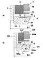
まず図1を参照してプラズマ処理装置の構成について説明する。図1において、真空チャンバ1の内部はプラズマ処理を行う処理室2となっており、減圧下でプラズマを発生させるための密閉された処理空間が形成可能となっている。処理室2は円筒形状となっており(図6参照)、処理室2の内部には、第1電極3(電極)および第2電極4が上下に対向して配設されている。第1電極3および第2電極4はそれぞれ円筒形状であり、処理室2内において同心配置となっている。
【0019】
第1電極3は、処理室2の底部を埋める形で装着された2層の絶縁体5A,5Bに周囲を取り囲まれ、処理室2の底の中央部に処理対象物を保持する上面を露呈させて固定された状態で配設されている。第1電極3はアルミニウムなどの導電体によって製作されており、円盤状の電極部3aから下方に支持部3bを延出させた形状となっている。そして支持部3bを絶縁部材5Cを介して真空チャンバ1に保持させることにより、電気的に絶縁された状態で装着されている。
【0020】
第2電極4は、第1電極3と同様にアルミニウムなどの導電体で製作されており、円盤状の電極部4aから上方に支持部4bを延出させた形状となっている。支持部4bは真空チャンバ1と電気的に導通しており、昇降機構24(図3)によって昇降可能となっている。第2電極4が下降した状態では、処理室2内の処理空間は、第2電極4によって機能が異なる2つの空間に仕切られる。
【0021】
すなわち、第2電極4の下方の第1電極3との間には放電空間2bが形成され、第2電極4の上方には真空チャンバ1の天井面との間に排気空間2aが形成される。放電空間2bは、第1電極3上に載置されたシリコンウェハ6を対象としてプラズマ処理を行うためのプラズマ放電を発生させる空間である。排気空間2aは、放電空間2b内のガスを外部に排気するための空間である。
【0022】
次に、図1,図2を参照して、第1電極3の詳細構造について説明する。第1電極3の電極部3aの上面は、処理対象物の基板であるシリコンウェハ6を載置する載置面となっており、シリコンウェハ6の外形よりも大きい形状となっている。ここでシリコンウェハ6は、表面側に論理回路が形成された半導体基板であり、回路形成面の裏側を機械加工によって研磨された後に、この裏面を対象としてプラズマ処理によるエッチングが行われる。そしてこのエッチングによって、機械加工により半導体基板の裏面に生成したマイクロクラックを除去する。
【0023】
図2に示すように、第1電極3の上面は、シリコンウェハ6を載置したときのシリコンウェハ6の外形位置P1よりも所定幅Cだけ内側に位置する境界線P2によって、内外2つの部分に分けられている。すなわち、境界線P2から内側は、素材の導電体であるアルミニウムが上面に露呈した上面中央部Aとなっており、境界線P2から外側は、上面中央部Aを環状に取り囲んで設けられ導電体のアルミニウムが絶縁被覆層3fによって覆われた上面外周部Bとなっている。ここで、所定幅Cは必ずしも全周にわたって等しい幅である必要はなく、位置によって異なってもよい。
【0024】
絶縁被覆層3fは、アルミナなどのセラミックによって形成されており、第1電極3が真空チャンバ1内に装着された状態では、図1に示すように、絶縁被覆層3fの外縁部は部分的に絶縁体5Aによって覆われる(図6も参照)。これにより、第1電極3の外縁部は放電空間2b内に発生したプラズマから絶縁され、異常放電の発生が防止される。
【0025】
図2に示すようにシリコンウェハ6の表面(図2において下面側)の回路形成面には保護テープ6aが貼着されており、プラズマ処理時には保護テープ6aを第1電極3の上面3gに向け、機械研磨面を上向きにした状態で載置される。保護テープ6aは、ポリオレフィン、ポリイミド、ポリエチレンテレフタレートなどの絶縁体の樹脂を100μm程度の厚みの膜に形成した樹脂テープであり、粘着材によりシリコンウェハ6の回路形成面に貼着される。シリコンウェハ6に貼着された保護テープ6aは、回路形成面(表面)に形成された絶縁層となっており、後述するようにこの絶縁層はシリコンウェハ6を静電吸着する際の誘電体として機能する。
【0026】
シリコンウェハ6を第1電極3に載置する際には、図2に示すように、シリコンウェハ6の保護テープ6aの中央部D、外縁部Eを、第1電極3の上面の上面中央部A、上面周辺部Bの絶縁被覆層3fに、それぞれ接触させて載置する。この状態では、外形位置P1から境界線P2までの範囲において、第1電極3の上面3gに保持されたシリコンウェハ6の保護テープ6aの外縁部Eと、絶縁被覆層3fとが重ね合わされて接触する。
【0027】
シリコンウェハ6を静電吸着する際には、主に保護テープ6aの中央部Dを静電吸着を行うための誘電体として利用して、シリコンウェハ6を上面中央部Aで静電吸着する。このとき外縁部Eの範囲においても保護テープ6aおよび絶縁被覆層3fを介してわずかながら静電吸着力が作用し、これらの静電吸着力によって、保護テープ6aの外縁部Eは絶縁被覆層3fに密着する。
【0028】
この密着状態では、第1電極3の上面において導電体が表面に露呈した上面中央部Aの外周端である境界線P2の位置は、シリコンウェハ6の外径寸法のばらつきや第1電極3上における載置位置にのばらつきに拘わらず、シリコンウェハ6によって覆われる。これにより、第1電極3の導電部は放電空間2b内のプラズマから確実に絶縁される。したがって、プラズマ放電中の第1電極3における異常放電を防止して、プラズマ処理装置の稼動状態を安定させることが可能となっている。
【0029】
図2に示すように、第1電極3には上面に開口する吸着孔3eが多数設けられており、吸着孔3eは第1電極3の内部に設けられた吸引孔3cに連通している。吸引孔3cはガスライン切り換え開閉機構11を介して真空吸着ポンプ12に接続されており、ガスライン切り換え開閉機構11は、図1に示すようにチッソガスを供給するN2ガス供給部13及びヘリウムガスを供給するHeガス供給部14に接続されている。ガスライン切り換え開閉機構11を切り換えることにより、吸引孔3cを真空吸着ポンプ12,N2ガス供給部13及びHeガス供給部14に選択的に接続させることができる。
【0030】
吸引孔3cが真空吸着ポンプ12と連通した状態で真空吸着ポンプ12を駆動することにより、吸着孔3eから真空吸引して第1電極3に載置されたシリコンウェハ6を真空吸着して保持する。したがって吸着孔3e、吸引孔3c、真空吸着ポンプ12は第1電極3の上面3gに開口した吸着孔3eから真空吸引することにより、シリコンウェハ6を真空吸着して保持する真空保持手段となっている。
【0031】
また、吸引孔3cをN2ガス供給部13またはHeガス供給部14に接続させることにより、吸着孔3eからシリコンウェハ6の下面に対してチッソガスまたはヘリウムガスを供給することができるようになっている。後述するように、チッソガスはシリコンウェハ6を載置面3gから強制的に離脱させる目的のブロー用ガスであり、ヘリウムガスはプラズマ処理時にシリコンウェハの冷却を促進する目的で吸着孔3e内に充填される熱伝達用のガスである。
【0032】
第1電極3には冷却用の冷媒流路3dが設けられており、冷媒流路3dは冷却機構10と接続されている。冷却機構10を駆動することにより、冷媒流路3d内を冷却水などの冷媒が循環し、これによりプラズマ処理時に発生した熱によって昇温した第1電極3や第1電極3上の保護テープ6aが冷却される。冷媒流路3dおよび冷却機構10は、第1電極3を冷却する冷却手段となっている。
【0033】
処理室2の排気空間2aに連通して設けられた排気ポート1aには、バルブ開放機構7を介して真空排気部8が接続されており、バルブ開放機構7を開放状態にして真空排気部8を駆動することにより、真空チャンバ1の処理室2内部が真空排気され、処理空2内が減圧される。真空排気部8は、排気空間2aに形成された排気ポート1aより排気を行って処理室2内を減圧する減圧手段となっている。
【0034】
第1電極3は、マッチング回路16を介して高周波電源部17に電気的に接続されている。高周波電源部17を駆動することにより、接地部19に接地された真空チャンバ1と導通した第2電極4と第1電極3の間には高周波電圧が印加され、これにより処理室2内部でプラズマ放電が発生する。マッチング回路16は、処理室2内でプラズマを発生させるプラズマ放電回路と高周波電源部17のインピーダンスを整合させる。第1電極3,第2電極4および高周波電源部17は、載置面に載置されたシリコンウェハ6をプラズマ処理するためのプラズマを発生するプラズマ発生手段となっている。
【0035】
また第1電極3には、RFフィルタ15を介して静電吸着用DC電源部18(直流電源部)が接続されている。静電吸着用DC電源部18を駆動することにより、第1電極3の表面には、負電荷が蓄積される。そしてこの状態で高周波電源部17を駆動して処理室2内にプラズマを発生させることにより、第1電極3上に載置されたシリコンウェハ6と接地部19とを接続する直流回路が処理室2内のプラズマを介して形成され、これにより、第1電極3,RFフィルタ15,静電吸着用DC電源部18,接地部19,プラズマ、シリコンウェハ6を順次結ぶ閉じた直流回路が形成され、シリコンウェハ6には正電荷が蓄積される。
【0036】
そして第1電極3に蓄積された負電荷とシリコンウェハ6に蓄積された正電荷との間にはクーロン力が作用し、このクーロン力によってシリコンウェハ6は誘電体としての保護テープ6aを介して第1電極3に保持される。このとき、RFフィルタ15は、高周波電源部17の高周波電圧が静電吸着用DC電源部18に直接印加されることを防止する。第1電極3,静電吸着用DC電源部18は、板状基板であるシリコンウェハ6を第1電極に静電吸着によって保持する静電吸着手段となっている。なお、静電吸着用DC電源部18の極性は正負逆でもよい。
【0037】
次に第2電極4の詳細構造について説明する。第2電極4は、中央の電極部4aと電極部4aを囲んで外周部に張り出して設けられた絶縁体からなる張出部4fを備えた構成となっている。張出部4fの外形は第1電極3よりも大きく、第1電極3よりも外側に広がった形状で配置されている。第2電極4の下面中央部には、ガス吹出部4eが設けられている。ガス吹出部4eは、放電空間2bにおいてプラズマ放電を発生するためのプラズマ発生用ガスを供給する。ガス吹出部4eは、内部に多数の微細孔を有する多孔質材料を円形の板状に加工した部材であり、ガス滞留空間4g内に供給されたプラズマ発生用ガスを、これらの微細孔を介して放電空間2b内に満遍なく吹き出させて均一な状態で供給する。
【0038】
支持部4b内には、ガス滞留空間4gに連通するガス供給孔4cが設けられており、ガス供給孔4cは開閉バルブ20を介してプラズマ発生用ガス供給部21に接続されている。開閉バルブ20を開にした状態でプラズマ発生用ガス供給部21を駆動することにより、フッ素系ガスを含んだプラズマ発生用ガスがガス吹出部4eより放電空間2b内に供給される。
【0039】
また第2電極4には冷却用の冷媒流路4dが設けられており、冷媒流路4dは冷却機構10と接続されている。冷却機構10を駆動することにより、冷媒流路4d内を冷却水などの冷媒が循環し、これによりプラズマ処理時に発生した熱によって昇温した第2電極4が冷却される。
【0040】
図3に示すように、処理室2の側面には、処理対象物の出し入れ用の開口部1bが設けられている(図5も参照)。開口部1bの外側には開閉機構23によって昇降する扉22が設けられており、扉22を昇降させることにより開口部1bが開閉される。図4は、扉22を下降させて開口部1bを開放した状態でシリコンウェハ6を出し入れする状態を示している。昇降機構24により第2電極4を上昇させて第1電極3上に搬送用のスペースを確保した状態で、アーム25aに保持された吸着ヘッド25を開口部1bを介して処理室2内に進入させることにより、シリコンウェハ6の出し入れが行われる。上記構成に示すように、排気空間2aが広く確保できるような構成とすることにより、第2電極4を上昇させる際の電極間距離を広く確保することができ、処理対象物の出し入れ操作を容易に行うことができる。
【0041】
ここで、図5を参照して、処理室2,第1電極3および第1電極3上に載置されるシリコンウェハ6、第2電極4の相互の平面位置関係について説明する。図5は、真空チャンバ1を水平方向に輪切りにした状態を示しており、図5に示す同心円は、外側から順に処理室2(真空チャンバ1)の内面2c、第2電極4の外側面4h(図6参照)、第1電極3の外側面3h、シリコンウェハ6の外形位置を示す境界線P1,第1電極3の上面における境界線P2を示している。
【0042】
図5から判るように、処理室2および第2電極4は略円筒形であり、したがって処理室2の内面2cと第2電極4の外側面4hとの間に形成された空間S1は、2つの同心円筒面に挟まれた円筒を開口部1bによって部分的に切り欠いた略円筒形状となっている。
【0043】
次に、放電空間2b内のガスを外周方向へ導くガス流路と、導かれたガスを排気空間2aに排気するガス排気路について説明する。図6に示すように、第2電極4が下降した状態では、処理室2(真空チャンバ1)の内面と第2電極4の張出部4fの側面4hとの間には、第2電極4の全周にわたって略均一な隙間G1を有する形状の空間S1が形成される。この空間S1は、放電空間2a内のガスを排気空間2bへ排気するガス排気路として機能する。
【0044】
また、張出部4fの下面と第1電極3の周囲に設けられた絶縁体5Aの上面との間には、第2電極4の全周にわたって略均一な隙間G2を有する形状の空間S2が形成される。この空間S2は、ガス吹出部4eから放電空間2b内に供給されたプラズマ発生用ガスや、プラズマ放電によって生成された反応ガスを外周方向に導くガス流路として機能する。
【0045】
ここで、上記隙間G1,G2はともに、排気空間2aの高さ方向の最大寸法H(図3参照)よりも狭くなるように、各部寸法が設定されている。これにより、ガスの流れやすさを示すコンダクタンスで比較した場合、ガス排気路としての空間S1,ガス流路としての空間S2におけるコンダクタンスを、排気空間2aにおけるコンダクタンスよりも小さくすることができる。
【0046】
減圧下にある処理室2内におけるプラズマ発生用ガスの流れ状態は、ガス分子の平均自由行程が大きい分子流の状態となっており、この分子流状態においてはコンダクタンスは圧力とは無関係にその空間の壁面間距離の3乗に比例する。したがって、前記の寸法Hに対してG1,G2が小さければ小さいほど、空間S1,S2におけるコンダクタンスは排気空間2aにおけるコンダクタンスよりも小さくなる。すなわち、減圧下で行われるプラズマ処理において、空間S1,S2内におけるガスの流れと比較して、排気空間2a内においてガスはより流れやすくなっている。
【0047】
したがって、プラズマ処理時に放電空間2b内のガスを排気ポート1aを介して排気する際に、空間S1から排気空間2a内に流入したガスはコンダクタンスが大きいことから速やかに排気ポート1aを介して排出され、排気空間2a内におけるガスの流動状態の分布に大きなばらつきが生じない。このため、空間S1から排気空間2a内に流入するガスについては、第2電極4の全周にわたってほぼ均一な流入状態が実現される。また、空間S2内のガスが空間S1内に流入する際においても同様に、第2電極4の全周にわたってほぼ均一な流れが実現される。これにより、放電空間2b内におけるガスの状態が均一化され、プラズマ処理によるエッチング分布を均一化することが可能となっている。
【0048】
このプラズマ処理装置は上記のように構成されており、以下プラズマ処理方法について各図を参照しながら説明する。このプラズマ処理は、表面に絶縁層としての保護テープ6aを有するシリコンウェハ6を第1電極3の上面に静電吸着によって保持した状態で、且つこの第1電極3を冷却しながらプラズマ処理を行うものである。
【0049】
先ず処理対象物であるシリコンウェハ6が処理室2内に搬送され、第1電極3上に載置される。この後開口部1bが閉じられ、真空吸着ポンプ12を駆動することにより、吸着孔3e、吸引孔3cを介して真空吸引し、シリコンウェハ6は第1電極3の上面3gに密着した状態で真空吸着により保持される。
【0050】
次いで真空排気部8を駆動して処理室2内を真空排気した後、プラズマ発生用ガス供給部21によってプラズマ発生用ガスが処理室2内に供給される。そしてこの後、静電吸着用DC電源部18を駆動してDC電圧を印加し、高周波電源部17を駆動してプラズマ放電を開始する。これにより放電空間2bにはプラズマが発生し、シリコンウェハ6を対象としたプラズマ処理が行われる。このプラズマ処理においては、第1電極3とシリコンウェハ6との間には静電吸着力が発生し、シリコンウェハ6は第1電極3に静電吸着力により保持される。
【0051】
この静電吸着においては、図2に示すようにシリコンウェハ6の保護テープ6aの中央部Dを第2電極3の上面中央部Aに接触させ、保護テープ6aの外縁部Eを第2電極3の上面周辺部Bの絶縁被覆層3fに接触させて載置する。そして主に保護テープ6aの中央部Dを静電吸着を行うための誘電体として利用してシリコンウェハ6を上面中央部Aで静電吸着するとともに、保護テープ6aの外縁部Eを絶縁被覆層3fに密着させることにより、プラズマと第1電極3の上面中央部Aとの間を絶縁する。
【0052】
この後、ガスライン切り替え開閉機構11を駆動して真空吸着をOFFし、バックHe導入が行われる。すなわち、真空吸引によるシリコンウェハ6の第1電極3への保持を解除した後に、Heガス供給部14から伝熱用のヘリウムガスを吸引孔3bを介して供給し、吸着孔3e内に充填する。このプラズマ処理においては、第1電極3は冷却機構10によって冷却されており、プラズマ処理によって昇温したシリコンウェハ6の熱を伝熱性に富む気体であるヘリウムガスを介して第1電極3に伝達することにより、シリコンウェハ6の冷却が効率よく行われる。
【0053】
そして所定のプラズマ処理時間が経過して放電を終了したならばバックHeを停止し、真空吸着を再びONする。これにより、プラズマ放電が終了することにより消失した静電吸着力に替えて、真空吸着力によってシリコンウェハ6が第1電極3に保持される。
【0054】
この後、静電吸着用DC電源部18を停止してDC電圧をOFFにし、大気開放機構9を駆動して処理室2内の大気開放を行う。この後、再びガスライン切り替え開閉機構11を駆動して真空吸着をOFFし、次いでウェハブローを行う。すなわちチッソガスを吸引孔3cを介して供給して吸着孔3eから噴出させ、シリコンウェハ6を第1電極3から離脱させる。そして開口部1bを開状態にし、シリコンウェハ6を処理室2の外部に搬送したならば、ウェハブローをOFFし、プラズマ処理の1サイクルを終了する。
【0055】
なお、上記実施形態における第1電極3の外縁部および絶縁被覆層3fの形状を、図7(b)に示すような形状に変更しても良い。図7(a)は、図1〜図6における第1電極3の外縁部および絶縁被覆層3fを対比のために示しており、図7(b)は、形状が変更された第1電極103,絶縁被覆層103fを示している。
【0056】
変更後の形状においては、第1電極103の外径D3は、図7(a)に示す第1電極3の外径D2よりも小さく設定されており、さらに第1電極103の外縁部の上面はR加工されている。そして絶縁被覆層103fは、図7(a)における境界線P2と同じ位置から外側の範囲に形成され、R加工された外縁部を覆うとともに第1電極103の外側面の上部を覆って形成されている。これにより、図7(a)に示す例と同様にプラズマ処理時における異常放電が防止される。また、絶縁被覆層103fはR形状となっていることから、クラックが発生しにくい形状となっている。
【0057】
上記構成を採用することにより、上記効果を確保しつつ第1電極103の外径D3を図7(a)に示す外径D2と比較して小さくすることができ、同一径D1のシリコンウェハを対象として、第1電極のコンパクト化が実現される。これにより、同一高周波電源出力でプラズマ処理を行った場合に、処理対象のシリコンウェハ6上でのプラズマ密度を向上させてより高速のエッチングを行うことができるとともに、真空チャンバ101の外形サイズB2を、図7(a)に示す真空チャンバ1の外形サイズB1と比較して小型化することができ、装置のコンパクト化が実現される。
【0058】
上記説明したように、本実施の形態のプラズマ処理装置は、絶縁層としての保護テープ6aが貼着されたシリコンウェハ6を静電吸着によって保持する第1電極3の上面を、導電体が上面に露呈した上面中央部Aと、この上面中央部を環状に取り囲んで設けられ導電体が絶縁被覆層によって覆われた上面外周部Bで構成している。
【0059】
このため、静電吸着によってシリコンウェハ6を保持する際には、上面中央部Aによって導電体を直接シリコンウェハ6に接触させて、シリコンウェハ6を十分な静電保持力で保持するとともに、シリコンウェハ6の保護テープ6aを第1電極3の導電体に密着させて冷却効率を向上させることができる。これにより、シリコンウェハ6や保護テープ6aの熱ダメージを防止するとともに、高エッチングレートの効率の良いプラズマ処理を実現することができる。
【0060】
さらに上記構成では、放電空間2b内のプラズマとの間で異常放電を発生しやすい第1電極3の外縁部を絶縁被覆層3fで覆うとともに、絶縁被覆層3fの内周端が必ずシリコンウェハ6で覆われるように寸法を設定していることから、プラズマ処理時の異常放電を防止して装置の安定稼動を実現できる。
【0061】
【発明の効果】
本発明によれば、基板を静電吸着によって保持する電極の上面を、基板の外形位置よりも所定幅だけ内側の境界線から内側に設けられ導電体が上面に露呈した上面中央部と、この上面中央部を環状に取り囲んで設けられ導電体が絶縁被覆層によって覆われた上面外周部で構成することにより、基板を十分な静電保持力で保持するとともに、基板を電極に密着させて基板の冷却効率を向上させることができる。
【図面の簡単な説明】
【図1】本発明の一実施の形態のプラズマ処理装置の側断面図
【図2】本発明の一実施の形態のプラズマ処理装置の第1電極の側断面図
【図3】本発明の一実施の形態のプラズマ処理装置の側断面図
【図4】本発明の一実施の形態のプラズマ処理装置の側断面図
【図5】本発明の一実施の形態のプラズマ処理装置の平断面図
【図6】本発明の一実施の形態のプラズマ処理装置の部分断面図
【図7】本発明の一実施の形態のプラズマ処理装置の部分断面図
【符号の説明】
1 真空チャンバ
2 処理室
3 第1電極
3f 絶縁被覆層
4 第2電極
6 シリコンウェハ
8 真空排気部
17 高周波電源部
18 静電吸着用DC電源部[0001]
BACKGROUND OF THE INVENTION
The present invention relates to a plasma processing apparatus for performing plasma processing on a semiconductor substrate such as a silicon wafer.In place It is related.
[0002]
[Prior art]
In a manufacturing process of a silicon wafer used in a semiconductor device, a thinning process is performed to reduce the thickness of the substrate as the semiconductor device is thinned. This thinning process is performed by mechanically polishing the back surface of the circuit forming surface after forming a circuit pattern on the surface of the silicon substrate. After the polishing process, the damage layer generated on the polished surface of the silicon substrate is mechanically polished. Plasma treatment is performed for the purpose of removing by etching.
[0003]
In this plasma processing, the silicon wafer needs to be held with the processing target surface (back surface) facing upward, so the silicon wafer is held with the circuit forming surface side facing the mounting surface of the substrate mounting portion. Is done. At this time, a protective tape is attached to the circuit forming surface for the purpose of preventing the circuit from directly contacting the mounting surface and receiving damage.
[0004]
[Problems to be solved by the invention]
As a method for holding such a silicon wafer, a method using electrostatic attraction is known. In this method, a silicon wafer is placed on a substrate mounting part whose surface is covered with a thin insulating layer, a DC voltage is applied to the conductor to make the surface of the substrate mounting part an electrostatic adsorption surface, The silicon wafer is held on the substrate mounting portion by applying a Coulomb force between the silicon wafer and the conductor under the insulating layer.
[0005]
However, when holding a silicon wafer with the above-mentioned protective tape attached thereto by electrostatic adsorption, the Coulomb force acts in the state of interposing an insulating protective tape in addition to the insulating layer. Compared to the case where the silicon wafer is directly adhered to the electrostatic attraction surface without using a tape, the electrostatic attraction force is low, and a sufficient holding force may not be obtained.
[0006]
In addition, since the entire surface of the substrate mounting portion is covered with the insulating layer, the silicon wafer is not in direct contact with the conductor of the substrate mounting portion when the silicon wafer is mounted, and the substrate mounting portion is removed from the silicon wafer. Low thermal conductivity. For this reason, it is difficult to efficiently remove heat from the silicon wafer and cool it during plasma processing. When the temperature of the substrate rises excessively, the protective tape attached to the substrate is subject to thermal damage. Therefore, in the setting of the plasma processing conditions, the power output during plasma processing is limited by the substrate cooling capacity of the substrate mounting part. Had to be set low. As described above, when a semiconductor substrate having an insulating layer is to be processed, it is difficult to improve cooling efficiency while ensuring sufficient electrostatic holding power, and it is difficult to realize plasma processing at a high etching rate. Met.
[0007]
Therefore, the present invention provides a plasma processing apparatus capable of holding a semiconductor substrate with a sufficient electrostatic holding force and improving the cooling efficiency of the semiconductor substrate.Place The purpose is to provide.
[0008]
[Means for Solving the Problems]
The plasma processing apparatus according to
[0009]
The plasma processing apparatus according to
[0011]
[0012]
[0016]
According to the present invention, the upper surface of the electrode that holds the substrate by electrostatic attraction is provided on the inner side from the boundary line on the inner side by a predetermined width from the outer position of the substrate, and the central portion of the upper surface where the conductor is exposed to the upper surface. The semiconductor substrate is held with a sufficient electrostatic holding force, and the substrate is brought into close contact with the electrode by comprising the upper surface outer peripheral portion that is provided so as to surround the central portion of the upper surface and is covered with an insulating coating layer. The cooling efficiency of the substrate can be improved.
[0017]
DETAILED DESCRIPTION OF THE INVENTION
Next, embodiments of the present invention will be described with reference to the drawings. FIG. 1 is a side sectional view of a plasma processing apparatus according to an embodiment of the present invention, FIG. 2 is a side sectional view of a first electrode of the plasma processing apparatus according to an embodiment of the present invention, and FIGS. FIG. 5 is a cross-sectional side view of a plasma processing apparatus according to an embodiment of the present invention, and FIGS. 6 and 7 are plasma processing apparatuses according to an embodiment of the present invention. FIG.
[0018]
First, the configuration of the plasma processing apparatus will be described with reference to FIG. In FIG. 1, the inside of a
[0019]
The
[0020]
Similar to the
[0021]
That is, a
[0022]
Next, the detailed structure of the
[0023]
As shown in FIG. 2, the upper surface of the
[0024]
The insulating
[0025]
As shown in FIG. 2, a
[0026]
When the
[0027]
When electrostatically attracting the
[0028]
In this close contact state, the position of the boundary line P2, which is the outer peripheral end of the upper surface central portion A where the conductor is exposed on the upper surface of the
[0029]
As shown in FIG. 2, the
[0030]
By driving the
[0031]
Further, the
[0032]
The
[0033]
A
[0034]
The
[0035]
The
[0036]
A Coulomb force acts between the negative charge accumulated in the
[0037]
Next, the detailed structure of the
[0038]
A
[0039]
The
[0040]
As shown in FIG. 3, an
[0041]
Here, with reference to FIG. 5, the mutual planar positional relationship between the
[0042]
As can be seen from FIG. 5, the
[0043]
Next, a gas flow path for guiding the gas in the
[0044]
Further, a space S2 having a shape having a substantially uniform gap G2 over the entire circumference of the
[0045]
Here, the dimensions of each part are set so that both of the gaps G1 and G2 are narrower than the maximum dimension H (see FIG. 3) in the height direction of the
[0046]
The flow state of the plasma generating gas in the
[0047]
Therefore, when the gas in the
[0048]
This plasma processing apparatus is configured as described above, and the plasma processing method will be described below with reference to the drawings. In this plasma treatment, the
[0049]
First, a
[0050]
Next, after the
[0051]
In this electrostatic adsorption, as shown in FIG. 2, the central portion D of the
[0052]
Thereafter, the gas line switching opening /
[0053]
When the discharge is finished after a predetermined plasma processing time has elapsed, the back He is stopped and the vacuum suction is turned on again. As a result, the
[0054]
Thereafter, the electrostatic power supply DC
[0055]
In addition, you may change the outer edge part of the
[0056]
In the changed shape, the outer diameter D3 of the
[0057]
By adopting the above configuration, the outer diameter D3 of the
[0058]
As described above, in the plasma processing apparatus of the present embodiment, the upper surface of the
[0059]
For this reason, when the
[0060]
Further, in the above configuration, the outer edge portion of the
[0061]
【The invention's effect】
According to the present invention, the upper surface of the electrode that holds the substrate by electrostatic attraction is provided on the inner side from the boundary line on the inner side by a predetermined width from the outer position of the substrate, and the central portion of the upper surface where the conductor is exposed to the upper surface. The substrate is formed by surrounding the upper surface in a ring shape and the outer periphery of the upper surface is covered with an insulating coating layer, so that the substrate is held with sufficient electrostatic holding force, and the substrate is brought into close contact with the electrode. The cooling efficiency can be improved.
[Brief description of the drawings]
FIG. 1 is a side sectional view of a plasma processing apparatus according to an embodiment of the present invention.
FIG. 2 is a side sectional view of a first electrode of a plasma processing apparatus according to an embodiment of the present invention.
FIG. 3 is a side sectional view of a plasma processing apparatus according to an embodiment of the present invention.
FIG. 4 is a side sectional view of a plasma processing apparatus according to an embodiment of the present invention.
FIG. 5 is a cross-sectional plan view of a plasma processing apparatus according to an embodiment of the present invention.
FIG. 6 is a partial sectional view of a plasma processing apparatus according to an embodiment of the present invention.
FIG. 7 is a partial cross-sectional view of a plasma processing apparatus according to an embodiment of the present invention.
[Explanation of symbols]
1 Vacuum chamber
2 treatment room
3 First electrode
3f Insulation coating layer
4 Second electrode
6 Silicon wafer
8 Vacuum exhaust part
17 High frequency power supply
18 DC power supply for electrostatic adsorption
Claims (4)
Translated fromJapanesePriority Applications (9)
| Application Number | Priority Date | Filing Date | Title |
|---|---|---|---|
| JP2002209052AJP4186536B2 (en) | 2002-07-18 | 2002-07-18 | Plasma processing equipment |
| KR1020057000947AKR100949953B1 (en) | 2002-07-18 | 2003-07-14 | Plasma processing apparatus and plasma processing method |
| EP03765292AEP1537596A1 (en) | 2002-07-18 | 2003-07-14 | Plasma processing apparatus and plasma processing method |
| AU2003243016AAU2003243016A1 (en) | 2002-07-18 | 2003-07-14 | Plasma processing apparatus and plasma processing method |
| PCT/JP2003/008930WO2004010456A1 (en) | 2002-07-18 | 2003-07-14 | Plasma processing apparatus and plasma processing method |
| CNB038170442ACN100429739C (en) | 2002-07-18 | 2003-07-14 | Plasma processing apparatus and plasma processing method |
| US10/621,497US7056831B2 (en) | 2002-07-18 | 2003-07-17 | Plasma processing apparatus and plasma processing method |
| TW092119656ATWI289892B (en) | 2002-07-18 | 2003-07-18 | Plasma processing apparatus and plasma processing method |
| US11/147,925US20050247404A1 (en) | 2002-07-18 | 2005-06-08 | Plasma processing apparatus and plasma processing method |
Applications Claiming Priority (1)
| Application Number | Priority Date | Filing Date | Title |
|---|---|---|---|
| JP2002209052AJP4186536B2 (en) | 2002-07-18 | 2002-07-18 | Plasma processing equipment |
Publications (2)
| Publication Number | Publication Date |
|---|---|
| JP2004055703A JP2004055703A (en) | 2004-02-19 |
| JP4186536B2true JP4186536B2 (en) | 2008-11-26 |
Family
ID=30767674
Family Applications (1)
| Application Number | Title | Priority Date | Filing Date |
|---|---|---|---|
| JP2002209052AExpired - Fee RelatedJP4186536B2 (en) | 2002-07-18 | 2002-07-18 | Plasma processing equipment |
Country Status (8)
| Country | Link |
|---|---|
| US (2) | US7056831B2 (en) |
| EP (1) | EP1537596A1 (en) |
| JP (1) | JP4186536B2 (en) |
| KR (1) | KR100949953B1 (en) |
| CN (1) | CN100429739C (en) |
| AU (1) | AU2003243016A1 (en) |
| TW (1) | TWI289892B (en) |
| WO (1) | WO2004010456A1 (en) |
Families Citing this family (337)
| Publication number | Priority date | Publication date | Assignee | Title |
|---|---|---|---|---|
| KR100455430B1 (en)* | 2002-03-29 | 2004-11-06 | 주식회사 엘지이아이 | Cooling apparatus for surface treatment device of heat exchanger and manufacturing method thereof |
| JP3992018B2 (en)* | 2003-07-23 | 2007-10-17 | 松下電器産業株式会社 | Plasma processing equipment |
| US20050051098A1 (en)* | 2003-09-05 | 2005-03-10 | Tooru Aramaki | Plasma processing apparatus |
| JP3894562B2 (en)* | 2003-10-01 | 2007-03-22 | キヤノン株式会社 | Substrate adsorption apparatus, exposure apparatus, and device manufacturing method |
| KR100727469B1 (en) | 2005-08-09 | 2007-06-13 | 세메스 주식회사 | Plasma Etching Equipment |
| JP4508054B2 (en)* | 2005-09-12 | 2010-07-21 | パナソニック株式会社 | Method for manufacturing electrode member |
| JP4674512B2 (en)* | 2005-09-12 | 2011-04-20 | パナソニック株式会社 | Plasma processing equipment |
| US20070212816A1 (en)* | 2006-03-08 | 2007-09-13 | Tokyo Electron Limited | Substrate processing system |
| US7985699B2 (en) | 2006-03-22 | 2011-07-26 | Tokyo Electron Limited | Substrate processing method and storage medium |
| JP4771845B2 (en)* | 2006-03-22 | 2011-09-14 | 東京エレクトロン株式会社 | Substrate processing method and storage medium |
| US20080141509A1 (en)* | 2006-12-19 | 2008-06-19 | Tokyo Electron Limited | Substrate processing system, substrate processing method, and storage medium |
| JP2008192642A (en)* | 2007-01-31 | 2008-08-21 | Tokyo Electron Ltd | Substrate processing apparatus |
| US8673080B2 (en) | 2007-10-16 | 2014-03-18 | Novellus Systems, Inc. | Temperature controlled showerhead |
| WO2009076568A2 (en)* | 2007-12-13 | 2009-06-18 | Lam Research Corporation | Plasma unconfinement sensor and methods thereof |
| US8252114B2 (en)* | 2008-03-28 | 2012-08-28 | Tokyo Electron Limited | Gas distribution system and method for distributing process gas in a processing system |
| US20100018463A1 (en)* | 2008-07-24 | 2010-01-28 | Chen-Hua Yu | Plural Gas Distribution System |
| KR101286545B1 (en)* | 2008-09-23 | 2013-07-17 | 엘지디스플레이 주식회사 | Washing device |
| JP5075793B2 (en)* | 2008-11-06 | 2012-11-21 | 東京エレクトロン株式会社 | Movable gas introduction structure and substrate processing apparatus |
| US9394608B2 (en) | 2009-04-06 | 2016-07-19 | Asm America, Inc. | Semiconductor processing reactor and components thereof |
| US8802201B2 (en) | 2009-08-14 | 2014-08-12 | Asm America, Inc. | Systems and methods for thin-film deposition of metal oxides using excited nitrogen-oxygen species |
| JP5432686B2 (en)* | 2009-12-03 | 2014-03-05 | 東京エレクトロン株式会社 | Plasma processing equipment |
| US9034142B2 (en)* | 2009-12-18 | 2015-05-19 | Novellus Systems, Inc. | Temperature controlled showerhead for high temperature operations |
| JP5567392B2 (en)* | 2010-05-25 | 2014-08-06 | 東京エレクトロン株式会社 | Plasma processing equipment |
| KR101937115B1 (en) | 2011-03-04 | 2019-01-09 | 노벨러스 시스템즈, 인코포레이티드 | Hybrid ceramic showerhead |
| JP5902896B2 (en)* | 2011-07-08 | 2016-04-13 | 東京エレクトロン株式会社 | Substrate processing equipment |
| US20130023129A1 (en) | 2011-07-20 | 2013-01-24 | Asm America, Inc. | Pressure transmitter for a semiconductor processing environment |
| US9017481B1 (en) | 2011-10-28 | 2015-04-28 | Asm America, Inc. | Process feed management for semiconductor substrate processing |
| US8980767B2 (en)* | 2012-01-13 | 2015-03-17 | Applied Materials, Inc. | Methods and apparatus for processing a substrate |
| CN103367089B (en)* | 2012-03-30 | 2016-04-06 | 中微半导体设备(上海)有限公司 | A kind of plasma processing apparatus with double casing |
| US10714315B2 (en) | 2012-10-12 | 2020-07-14 | Asm Ip Holdings B.V. | Semiconductor reaction chamber showerhead |
| US10727092B2 (en)* | 2012-10-17 | 2020-07-28 | Applied Materials, Inc. | Heated substrate support ring |
| JP5886821B2 (en)* | 2013-01-04 | 2016-03-16 | ピーエスケー インコーポレイテッド | Substrate processing apparatus and method |
| US20160376700A1 (en) | 2013-02-01 | 2016-12-29 | Asm Ip Holding B.V. | System for treatment of deposition reactor |
| US11015245B2 (en) | 2014-03-19 | 2021-05-25 | Asm Ip Holding B.V. | Gas-phase reactor and system having exhaust plenum and components thereof |
| US10741365B2 (en) | 2014-05-05 | 2020-08-11 | Lam Research Corporation | Low volume showerhead with porous baffle |
| JP6225837B2 (en)* | 2014-06-04 | 2017-11-08 | 東京エレクトロン株式会社 | Film forming apparatus, film forming method, storage medium |
| US10858737B2 (en) | 2014-07-28 | 2020-12-08 | Asm Ip Holding B.V. | Showerhead assembly and components thereof |
| US9890456B2 (en) | 2014-08-21 | 2018-02-13 | Asm Ip Holding B.V. | Method and system for in situ formation of gas-phase compounds |
| US10941490B2 (en) | 2014-10-07 | 2021-03-09 | Asm Ip Holding B.V. | Multiple temperature range susceptor, assembly, reactor and system including the susceptor, and methods of using the same |
| JP6380094B2 (en)* | 2014-12-26 | 2018-08-29 | 東京エレクトロン株式会社 | Mounting table and plasma processing apparatus |
| US10276355B2 (en) | 2015-03-12 | 2019-04-30 | Asm Ip Holding B.V. | Multi-zone reactor, system including the reactor, and method of using the same |
| US10378107B2 (en) | 2015-05-22 | 2019-08-13 | Lam Research Corporation | Low volume showerhead with faceplate holes for improved flow uniformity |
| US10023959B2 (en) | 2015-05-26 | 2018-07-17 | Lam Research Corporation | Anti-transient showerhead |
| US10458018B2 (en) | 2015-06-26 | 2019-10-29 | Asm Ip Holding B.V. | Structures including metal carbide material, devices including the structures, and methods of forming same |
| US10211308B2 (en) | 2015-10-21 | 2019-02-19 | Asm Ip Holding B.V. | NbMC layers |
| US10358721B2 (en)* | 2015-10-22 | 2019-07-23 | Asm Ip Holding B.V. | Semiconductor manufacturing system including deposition apparatus |
| US11139308B2 (en) | 2015-12-29 | 2021-10-05 | Asm Ip Holding B.V. | Atomic layer deposition of III-V compounds to form V-NAND devices |
| US10529554B2 (en) | 2016-02-19 | 2020-01-07 | Asm Ip Holding B.V. | Method for forming silicon nitride film selectively on sidewalls or flat surfaces of trenches |
| US10343920B2 (en) | 2016-03-18 | 2019-07-09 | Asm Ip Holding B.V. | Aligned carbon nanotubes |
| US10190213B2 (en) | 2016-04-21 | 2019-01-29 | Asm Ip Holding B.V. | Deposition of metal borides |
| US10865475B2 (en) | 2016-04-21 | 2020-12-15 | Asm Ip Holding B.V. | Deposition of metal borides and silicides |
| US10367080B2 (en) | 2016-05-02 | 2019-07-30 | Asm Ip Holding B.V. | Method of forming a germanium oxynitride film |
| US11453943B2 (en) | 2016-05-25 | 2022-09-27 | Asm Ip Holding B.V. | Method for forming carbon-containing silicon/metal oxide or nitride film by ALD using silicon precursor and hydrocarbon precursor |
| JP6880076B2 (en)* | 2016-06-03 | 2021-06-02 | アプライド マテリアルズ インコーポレイテッドApplied Materials,Incorporated | Board distance monitoring |
| US10612137B2 (en) | 2016-07-08 | 2020-04-07 | Asm Ip Holdings B.V. | Organic reactants for atomic layer deposition |
| US9859151B1 (en) | 2016-07-08 | 2018-01-02 | Asm Ip Holding B.V. | Selective film deposition method to form air gaps |
| US9887082B1 (en) | 2016-07-28 | 2018-02-06 | Asm Ip Holding B.V. | Method and apparatus for filling a gap |
| US9812320B1 (en) | 2016-07-28 | 2017-11-07 | Asm Ip Holding B.V. | Method and apparatus for filling a gap |
| KR102532607B1 (en) | 2016-07-28 | 2023-05-15 | 에이에스엠 아이피 홀딩 비.브이. | Substrate processing apparatus and method of operating the same |
| US10643826B2 (en) | 2016-10-26 | 2020-05-05 | Asm Ip Holdings B.V. | Methods for thermally calibrating reaction chambers |
| US11532757B2 (en) | 2016-10-27 | 2022-12-20 | Asm Ip Holding B.V. | Deposition of charge trapping layers |
| US10229833B2 (en) | 2016-11-01 | 2019-03-12 | Asm Ip Holding B.V. | Methods for forming a transition metal nitride film on a substrate by atomic layer deposition and related semiconductor device structures |
| US10714350B2 (en) | 2016-11-01 | 2020-07-14 | ASM IP Holdings, B.V. | Methods for forming a transition metal niobium nitride film on a substrate by atomic layer deposition and related semiconductor device structures |
| KR102546317B1 (en) | 2016-11-15 | 2023-06-21 | 에이에스엠 아이피 홀딩 비.브이. | Gas supply unit and substrate processing apparatus including the same |
| JP6886128B2 (en) | 2016-11-29 | 2021-06-16 | 住友電気工業株式会社 | Wafer holder |
| KR102762543B1 (en) | 2016-12-14 | 2025-02-05 | 에이에스엠 아이피 홀딩 비.브이. | Substrate processing apparatus |
| US11581186B2 (en) | 2016-12-15 | 2023-02-14 | Asm Ip Holding B.V. | Sequential infiltration synthesis apparatus |
| US11447861B2 (en) | 2016-12-15 | 2022-09-20 | Asm Ip Holding B.V. | Sequential infiltration synthesis apparatus and a method of forming a patterned structure |
| KR102700194B1 (en)* | 2016-12-19 | 2024-08-28 | 에이에스엠 아이피 홀딩 비.브이. | Substrate processing apparatus |
| US10269558B2 (en) | 2016-12-22 | 2019-04-23 | Asm Ip Holding B.V. | Method of forming a structure on a substrate |
| US10867788B2 (en) | 2016-12-28 | 2020-12-15 | Asm Ip Holding B.V. | Method of forming a structure on a substrate |
| US11390950B2 (en) | 2017-01-10 | 2022-07-19 | Asm Ip Holding B.V. | Reactor system and method to reduce residue buildup during a film deposition process |
| US10468261B2 (en) | 2017-02-15 | 2019-11-05 | Asm Ip Holding B.V. | Methods for forming a metallic film on a substrate by cyclical deposition and related semiconductor device structures |
| US10529563B2 (en) | 2017-03-29 | 2020-01-07 | Asm Ip Holdings B.V. | Method for forming doped metal oxide films on a substrate by cyclical deposition and related semiconductor device structures |
| KR102457289B1 (en) | 2017-04-25 | 2022-10-21 | 에이에스엠 아이피 홀딩 비.브이. | Method for depositing a thin film and manufacturing a semiconductor device |
| US10770286B2 (en) | 2017-05-08 | 2020-09-08 | Asm Ip Holdings B.V. | Methods for selectively forming a silicon nitride film on a substrate and related semiconductor device structures |
| US10892156B2 (en) | 2017-05-08 | 2021-01-12 | Asm Ip Holding B.V. | Methods for forming a silicon nitride film on a substrate and related semiconductor device structures |
| US10886123B2 (en) | 2017-06-02 | 2021-01-05 | Asm Ip Holding B.V. | Methods for forming low temperature semiconductor layers and related semiconductor device structures |
| US12040200B2 (en) | 2017-06-20 | 2024-07-16 | Asm Ip Holding B.V. | Semiconductor processing apparatus and methods for calibrating a semiconductor processing apparatus |
| US11306395B2 (en) | 2017-06-28 | 2022-04-19 | Asm Ip Holding B.V. | Methods for depositing a transition metal nitride film on a substrate by atomic layer deposition and related deposition apparatus |
| KR20190009245A (en) | 2017-07-18 | 2019-01-28 | 에이에스엠 아이피 홀딩 비.브이. | Methods for forming a semiconductor device structure and related semiconductor device structures |
| US11374112B2 (en) | 2017-07-19 | 2022-06-28 | Asm Ip Holding B.V. | Method for depositing a group IV semiconductor and related semiconductor device structures |
| US11018002B2 (en) | 2017-07-19 | 2021-05-25 | Asm Ip Holding B.V. | Method for selectively depositing a Group IV semiconductor and related semiconductor device structures |
| US10541333B2 (en) | 2017-07-19 | 2020-01-21 | Asm Ip Holding B.V. | Method for depositing a group IV semiconductor and related semiconductor device structures |
| US10590535B2 (en) | 2017-07-26 | 2020-03-17 | Asm Ip Holdings B.V. | Chemical treatment, deposition and/or infiltration apparatus and method for using the same |
| TWI815813B (en) | 2017-08-04 | 2023-09-21 | 荷蘭商Asm智慧財產控股公司 | Showerhead assembly for distributing a gas within a reaction chamber |
| US10770336B2 (en) | 2017-08-08 | 2020-09-08 | Asm Ip Holding B.V. | Substrate lift mechanism and reactor including same |
| US10692741B2 (en) | 2017-08-08 | 2020-06-23 | Asm Ip Holdings B.V. | Radiation shield |
| US11769682B2 (en) | 2017-08-09 | 2023-09-26 | Asm Ip Holding B.V. | Storage apparatus for storing cassettes for substrates and processing apparatus equipped therewith |
| US11139191B2 (en) | 2017-08-09 | 2021-10-05 | Asm Ip Holding B.V. | Storage apparatus for storing cassettes for substrates and processing apparatus equipped therewith |
| US11830730B2 (en) | 2017-08-29 | 2023-11-28 | Asm Ip Holding B.V. | Layer forming method and apparatus |
| US11056344B2 (en) | 2017-08-30 | 2021-07-06 | Asm Ip Holding B.V. | Layer forming method |
| KR102491945B1 (en) | 2017-08-30 | 2023-01-26 | 에이에스엠 아이피 홀딩 비.브이. | Substrate processing apparatus |
| US11295980B2 (en) | 2017-08-30 | 2022-04-05 | Asm Ip Holding B.V. | Methods for depositing a molybdenum metal film over a dielectric surface of a substrate by a cyclical deposition process and related semiconductor device structures |
| KR102401446B1 (en) | 2017-08-31 | 2022-05-24 | 에이에스엠 아이피 홀딩 비.브이. | Substrate processing apparatus |
| KR102630301B1 (en) | 2017-09-21 | 2024-01-29 | 에이에스엠 아이피 홀딩 비.브이. | Method of sequential infiltration synthesis treatment of infiltrateable material and structures and devices formed using same |
| US10844484B2 (en) | 2017-09-22 | 2020-11-24 | Asm Ip Holding B.V. | Apparatus for dispensing a vapor phase reactant to a reaction chamber and related methods |
| US10658205B2 (en) | 2017-09-28 | 2020-05-19 | Asm Ip Holdings B.V. | Chemical dispensing apparatus and methods for dispensing a chemical to a reaction chamber |
| US10403504B2 (en) | 2017-10-05 | 2019-09-03 | Asm Ip Holding B.V. | Method for selectively depositing a metallic film on a substrate |
| US10923344B2 (en) | 2017-10-30 | 2021-02-16 | Asm Ip Holding B.V. | Methods for forming a semiconductor structure and related semiconductor structures |
| US10910262B2 (en) | 2017-11-16 | 2021-02-02 | Asm Ip Holding B.V. | Method of selectively depositing a capping layer structure on a semiconductor device structure |
| US11022879B2 (en) | 2017-11-24 | 2021-06-01 | Asm Ip Holding B.V. | Method of forming an enhanced unexposed photoresist layer |
| CN111344522B (en) | 2017-11-27 | 2022-04-12 | 阿斯莫Ip控股公司 | Including clean mini-environment device |
| WO2019103613A1 (en) | 2017-11-27 | 2019-05-31 | Asm Ip Holding B.V. | A storage device for storing wafer cassettes for use with a batch furnace |
| US10872771B2 (en) | 2018-01-16 | 2020-12-22 | Asm Ip Holding B. V. | Method for depositing a material film on a substrate within a reaction chamber by a cyclical deposition process and related device structures |
| KR102695659B1 (en) | 2018-01-19 | 2024-08-14 | 에이에스엠 아이피 홀딩 비.브이. | Method for depositing a gap filling layer by plasma assisted deposition |
| TWI799494B (en) | 2018-01-19 | 2023-04-21 | 荷蘭商Asm 智慧財產控股公司 | Deposition method |
| US11018047B2 (en) | 2018-01-25 | 2021-05-25 | Asm Ip Holding B.V. | Hybrid lift pin |
| USD880437S1 (en) | 2018-02-01 | 2020-04-07 | Asm Ip Holding B.V. | Gas supply plate for semiconductor manufacturing apparatus |
| US11081345B2 (en) | 2018-02-06 | 2021-08-03 | Asm Ip Holding B.V. | Method of post-deposition treatment for silicon oxide film |
| WO2019158960A1 (en) | 2018-02-14 | 2019-08-22 | Asm Ip Holding B.V. | A method for depositing a ruthenium-containing film on a substrate by a cyclical deposition process |
| US10896820B2 (en) | 2018-02-14 | 2021-01-19 | Asm Ip Holding B.V. | Method for depositing a ruthenium-containing film on a substrate by a cyclical deposition process |
| US10731249B2 (en) | 2018-02-15 | 2020-08-04 | Asm Ip Holding B.V. | Method of forming a transition metal containing film on a substrate by a cyclical deposition process, a method for supplying a transition metal halide compound to a reaction chamber, and related vapor deposition apparatus |
| KR102636427B1 (en) | 2018-02-20 | 2024-02-13 | 에이에스엠 아이피 홀딩 비.브이. | Substrate processing method and apparatus |
| US10975470B2 (en) | 2018-02-23 | 2021-04-13 | Asm Ip Holding B.V. | Apparatus for detecting or monitoring for a chemical precursor in a high temperature environment |
| US11473195B2 (en) | 2018-03-01 | 2022-10-18 | Asm Ip Holding B.V. | Semiconductor processing apparatus and a method for processing a substrate |
| US11629406B2 (en) | 2018-03-09 | 2023-04-18 | Asm Ip Holding B.V. | Semiconductor processing apparatus comprising one or more pyrometers for measuring a temperature of a substrate during transfer of the substrate |
| US11114283B2 (en) | 2018-03-16 | 2021-09-07 | Asm Ip Holding B.V. | Reactor, system including the reactor, and methods of manufacturing and using same |
| KR102646467B1 (en) | 2018-03-27 | 2024-03-11 | 에이에스엠 아이피 홀딩 비.브이. | Method of forming an electrode on a substrate and a semiconductor device structure including an electrode |
| US11088002B2 (en) | 2018-03-29 | 2021-08-10 | Asm Ip Holding B.V. | Substrate rack and a substrate processing system and method |
| US11230766B2 (en) | 2018-03-29 | 2022-01-25 | Asm Ip Holding B.V. | Substrate processing apparatus and method |
| KR102501472B1 (en) | 2018-03-30 | 2023-02-20 | 에이에스엠 아이피 홀딩 비.브이. | Substrate processing method |
| KR102600229B1 (en) | 2018-04-09 | 2023-11-10 | 에이에스엠 아이피 홀딩 비.브이. | Substrate supporting device, substrate processing apparatus including the same and substrate processing method |
| US12025484B2 (en) | 2018-05-08 | 2024-07-02 | Asm Ip Holding B.V. | Thin film forming method |
| TWI811348B (en) | 2018-05-08 | 2023-08-11 | 荷蘭商Asm 智慧財產控股公司 | Methods for depositing an oxide film on a substrate by a cyclical deposition process and related device structures |
| US12272527B2 (en) | 2018-05-09 | 2025-04-08 | Asm Ip Holding B.V. | Apparatus for use with hydrogen radicals and method of using same |
| KR20190129718A (en) | 2018-05-11 | 2019-11-20 | 에이에스엠 아이피 홀딩 비.브이. | Methods for forming a doped metal carbide film on a substrate and related semiconductor device structures |
| KR102596988B1 (en) | 2018-05-28 | 2023-10-31 | 에이에스엠 아이피 홀딩 비.브이. | Method of processing a substrate and a device manufactured by the same |
| TWI840362B (en) | 2018-06-04 | 2024-05-01 | 荷蘭商Asm Ip私人控股有限公司 | Wafer handling chamber with moisture reduction |
| US11718913B2 (en) | 2018-06-04 | 2023-08-08 | Asm Ip Holding B.V. | Gas distribution system and reactor system including same |
| US11286562B2 (en) | 2018-06-08 | 2022-03-29 | Asm Ip Holding B.V. | Gas-phase chemical reactor and method of using same |
| KR102568797B1 (en) | 2018-06-21 | 2023-08-21 | 에이에스엠 아이피 홀딩 비.브이. | Substrate processing system |
| US10797133B2 (en) | 2018-06-21 | 2020-10-06 | Asm Ip Holding B.V. | Method for depositing a phosphorus doped silicon arsenide film and related semiconductor device structures |
| TWI873894B (en) | 2018-06-27 | 2025-02-21 | 荷蘭商Asm Ip私人控股有限公司 | Cyclic deposition methods for forming metal-containing material and films and structures including the metal-containing material |
| KR102854019B1 (en) | 2018-06-27 | 2025-09-02 | 에이에스엠 아이피 홀딩 비.브이. | Periodic deposition method for forming a metal-containing material and films and structures comprising the metal-containing material |
| KR102686758B1 (en) | 2018-06-29 | 2024-07-18 | 에이에스엠 아이피 홀딩 비.브이. | Method for depositing a thin film and manufacturing a semiconductor device |
| US10612136B2 (en) | 2018-06-29 | 2020-04-07 | ASM IP Holding, B.V. | Temperature-controlled flange and reactor system including same |
| US10388513B1 (en) | 2018-07-03 | 2019-08-20 | Asm Ip Holding B.V. | Method for depositing silicon-free carbon-containing film as gap-fill layer by pulse plasma-assisted deposition |
| US10755922B2 (en) | 2018-07-03 | 2020-08-25 | Asm Ip Holding B.V. | Method for depositing silicon-free carbon-containing film as gap-fill layer by pulse plasma-assisted deposition |
| US10767789B2 (en) | 2018-07-16 | 2020-09-08 | Asm Ip Holding B.V. | Diaphragm valves, valve components, and methods for forming valve components |
| US11053591B2 (en) | 2018-08-06 | 2021-07-06 | Asm Ip Holding B.V. | Multi-port gas injection system and reactor system including same |
| US10883175B2 (en) | 2018-08-09 | 2021-01-05 | Asm Ip Holding B.V. | Vertical furnace for processing substrates and a liner for use therein |
| US10829852B2 (en) | 2018-08-16 | 2020-11-10 | Asm Ip Holding B.V. | Gas distribution device for a wafer processing apparatus |
| US11430674B2 (en) | 2018-08-22 | 2022-08-30 | Asm Ip Holding B.V. | Sensor array, apparatus for dispensing a vapor phase reactant to a reaction chamber and related methods |
| KR102707956B1 (en) | 2018-09-11 | 2024-09-19 | 에이에스엠 아이피 홀딩 비.브이. | Method for deposition of a thin film |
| US11024523B2 (en) | 2018-09-11 | 2021-06-01 | Asm Ip Holding B.V. | Substrate processing apparatus and method |
| US11049751B2 (en) | 2018-09-14 | 2021-06-29 | Asm Ip Holding B.V. | Cassette supply system to store and handle cassettes and processing apparatus equipped therewith |
| CN109087840B (en)* | 2018-09-27 | 2023-11-07 | 中山市博顿光电科技有限公司 | Water-cooled radio frequency neutralizer |
| CN110970344B (en) | 2018-10-01 | 2024-10-25 | Asmip控股有限公司 | Substrate holding apparatus, system comprising the same and method of using the same |
| US11232963B2 (en) | 2018-10-03 | 2022-01-25 | Asm Ip Holding B.V. | Substrate processing apparatus and method |
| KR102592699B1 (en) | 2018-10-08 | 2023-10-23 | 에이에스엠 아이피 홀딩 비.브이. | Substrate support unit and apparatuses for depositing thin film and processing the substrate including the same |
| KR102546322B1 (en) | 2018-10-19 | 2023-06-21 | 에이에스엠 아이피 홀딩 비.브이. | Substrate processing apparatus and substrate processing method |
| KR102605121B1 (en) | 2018-10-19 | 2023-11-23 | 에이에스엠 아이피 홀딩 비.브이. | Substrate processing apparatus and substrate processing method |
| USD948463S1 (en) | 2018-10-24 | 2022-04-12 | Asm Ip Holding B.V. | Susceptor for semiconductor substrate supporting apparatus |
| US12378665B2 (en) | 2018-10-26 | 2025-08-05 | Asm Ip Holding B.V. | High temperature coatings for a preclean and etch apparatus and related methods |
| US11087997B2 (en) | 2018-10-31 | 2021-08-10 | Asm Ip Holding B.V. | Substrate processing apparatus for processing substrates |
| KR102748291B1 (en) | 2018-11-02 | 2024-12-31 | 에이에스엠 아이피 홀딩 비.브이. | Substrate support unit and substrate processing apparatus including the same |
| US11572620B2 (en) | 2018-11-06 | 2023-02-07 | Asm Ip Holding B.V. | Methods for selectively depositing an amorphous silicon film on a substrate |
| US11031242B2 (en) | 2018-11-07 | 2021-06-08 | Asm Ip Holding B.V. | Methods for depositing a boron doped silicon germanium film |
| US10847366B2 (en) | 2018-11-16 | 2020-11-24 | Asm Ip Holding B.V. | Methods for depositing a transition metal chalcogenide film on a substrate by a cyclical deposition process |
| US10818758B2 (en) | 2018-11-16 | 2020-10-27 | Asm Ip Holding B.V. | Methods for forming a metal silicate film on a substrate in a reaction chamber and related semiconductor device structures |
| US12040199B2 (en) | 2018-11-28 | 2024-07-16 | Asm Ip Holding B.V. | Substrate processing apparatus for processing substrates |
| US11217444B2 (en) | 2018-11-30 | 2022-01-04 | Asm Ip Holding B.V. | Method for forming an ultraviolet radiation responsive metal oxide-containing film |
| KR102636428B1 (en) | 2018-12-04 | 2024-02-13 | 에이에스엠 아이피 홀딩 비.브이. | A method for cleaning a substrate processing apparatus |
| US11158513B2 (en) | 2018-12-13 | 2021-10-26 | Asm Ip Holding B.V. | Methods for forming a rhenium-containing film on a substrate by a cyclical deposition process and related semiconductor device structures |
| TWI874340B (en) | 2018-12-14 | 2025-03-01 | 荷蘭商Asm Ip私人控股有限公司 | Method of forming device structure, structure formed by the method and system for performing the method |
| TWI866480B (en) | 2019-01-17 | 2024-12-11 | 荷蘭商Asm Ip 私人控股有限公司 | Methods of forming a transition metal containing film on a substrate by a cyclical deposition process |
| KR102727227B1 (en) | 2019-01-22 | 2024-11-07 | 에이에스엠 아이피 홀딩 비.브이. | Semiconductor processing device |
| CN111524788B (en) | 2019-02-01 | 2023-11-24 | Asm Ip私人控股有限公司 | Method for forming topologically selective films of silicon oxide |
| KR102626263B1 (en) | 2019-02-20 | 2024-01-16 | 에이에스엠 아이피 홀딩 비.브이. | Cyclical deposition method including treatment step and apparatus for same |
| TWI873122B (en) | 2019-02-20 | 2025-02-21 | 荷蘭商Asm Ip私人控股有限公司 | Method of filling a recess formed within a surface of a substrate, semiconductor structure formed according to the method, and semiconductor processing apparatus |
| TWI845607B (en) | 2019-02-20 | 2024-06-21 | 荷蘭商Asm Ip私人控股有限公司 | Cyclical deposition method and apparatus for filling a recess formed within a substrate surface |
| TWI838458B (en) | 2019-02-20 | 2024-04-11 | 荷蘭商Asm Ip私人控股有限公司 | Apparatus and methods for plug fill deposition in 3-d nand applications |
| TWI842826B (en) | 2019-02-22 | 2024-05-21 | 荷蘭商Asm Ip私人控股有限公司 | Substrate processing apparatus and method for processing substrate |
| KR102858005B1 (en) | 2019-03-08 | 2025-09-09 | 에이에스엠 아이피 홀딩 비.브이. | Method for Selective Deposition of Silicon Nitride Layer and Structure Including Selectively-Deposited Silicon Nitride Layer |
| KR102782593B1 (en) | 2019-03-08 | 2025-03-14 | 에이에스엠 아이피 홀딩 비.브이. | Structure Including SiOC Layer and Method of Forming Same |
| US11742198B2 (en) | 2019-03-08 | 2023-08-29 | Asm Ip Holding B.V. | Structure including SiOCN layer and method of forming same |
| JP2020167398A (en) | 2019-03-28 | 2020-10-08 | エーエスエム・アイピー・ホールディング・ベー・フェー | Door openers and substrate processing equipment provided with door openers |
| KR102809999B1 (en) | 2019-04-01 | 2025-05-19 | 에이에스엠 아이피 홀딩 비.브이. | Method of manufacturing semiconductor device |
| KR20200123380A (en) | 2019-04-19 | 2020-10-29 | 에이에스엠 아이피 홀딩 비.브이. | Layer forming method and apparatus |
| KR20200125453A (en) | 2019-04-24 | 2020-11-04 | 에이에스엠 아이피 홀딩 비.브이. | Gas-phase reactor system and method of using same |
| KR20200130121A (en) | 2019-05-07 | 2020-11-18 | 에이에스엠 아이피 홀딩 비.브이. | Chemical source vessel with dip tube |
| US11289326B2 (en) | 2019-05-07 | 2022-03-29 | Asm Ip Holding B.V. | Method for reforming amorphous carbon polymer film |
| KR20200130652A (en) | 2019-05-10 | 2020-11-19 | 에이에스엠 아이피 홀딩 비.브이. | Method of depositing material onto a surface and structure formed according to the method |
| JP7598201B2 (en) | 2019-05-16 | 2024-12-11 | エーエスエム・アイピー・ホールディング・ベー・フェー | Wafer boat handling apparatus, vertical batch furnace and method |
| JP7612342B2 (en) | 2019-05-16 | 2025-01-14 | エーエスエム・アイピー・ホールディング・ベー・フェー | Wafer boat handling apparatus, vertical batch furnace and method |
| USD947913S1 (en) | 2019-05-17 | 2022-04-05 | Asm Ip Holding B.V. | Susceptor shaft |
| USD975665S1 (en) | 2019-05-17 | 2023-01-17 | Asm Ip Holding B.V. | Susceptor shaft |
| USD935572S1 (en) | 2019-05-24 | 2021-11-09 | Asm Ip Holding B.V. | Gas channel plate |
| USD922229S1 (en) | 2019-06-05 | 2021-06-15 | Asm Ip Holding B.V. | Device for controlling a temperature of a gas supply unit |
| KR20200141002A (en) | 2019-06-06 | 2020-12-17 | 에이에스엠 아이피 홀딩 비.브이. | Method of using a gas-phase reactor system including analyzing exhausted gas |
| KR20200141931A (en) | 2019-06-10 | 2020-12-21 | 에이에스엠 아이피 홀딩 비.브이. | Method for cleaning quartz epitaxial chambers |
| KR20200143254A (en) | 2019-06-11 | 2020-12-23 | 에이에스엠 아이피 홀딩 비.브이. | Method of forming an electronic structure using an reforming gas, system for performing the method, and structure formed using the method |
| USD944946S1 (en) | 2019-06-14 | 2022-03-01 | Asm Ip Holding B.V. | Shower plate |
| USD931978S1 (en) | 2019-06-27 | 2021-09-28 | Asm Ip Holding B.V. | Showerhead vacuum transport |
| KR20210005515A (en) | 2019-07-03 | 2021-01-14 | 에이에스엠 아이피 홀딩 비.브이. | Temperature control assembly for substrate processing apparatus and method of using same |
| JP7499079B2 (en) | 2019-07-09 | 2024-06-13 | エーエスエム・アイピー・ホールディング・ベー・フェー | Plasma device using coaxial waveguide and substrate processing method |
| CN112216646A (en) | 2019-07-10 | 2021-01-12 | Asm Ip私人控股有限公司 | Substrate supporting assembly and substrate processing device comprising same |
| KR20210010307A (en) | 2019-07-16 | 2021-01-27 | 에이에스엠 아이피 홀딩 비.브이. | Substrate processing apparatus |
| KR102860110B1 (en) | 2019-07-17 | 2025-09-16 | 에이에스엠 아이피 홀딩 비.브이. | Methods of forming silicon germanium structures |
| KR20210010816A (en) | 2019-07-17 | 2021-01-28 | 에이에스엠 아이피 홀딩 비.브이. | Radical assist ignition plasma system and method |
| US11643724B2 (en) | 2019-07-18 | 2023-05-09 | Asm Ip Holding B.V. | Method of forming structures using a neutral beam |
| KR20210010817A (en) | 2019-07-19 | 2021-01-28 | 에이에스엠 아이피 홀딩 비.브이. | Method of Forming Topology-Controlled Amorphous Carbon Polymer Film |
| TWI839544B (en) | 2019-07-19 | 2024-04-21 | 荷蘭商Asm Ip私人控股有限公司 | Method of forming topology-controlled amorphous carbon polymer film |
| TWI851767B (en) | 2019-07-29 | 2024-08-11 | 荷蘭商Asm Ip私人控股有限公司 | Methods for selective deposition utilizing n-type dopants and/or alternative dopants to achieve high dopant incorporation |
| CN112309900A (en) | 2019-07-30 | 2021-02-02 | Asm Ip私人控股有限公司 | Substrate processing apparatus |
| US12169361B2 (en) | 2019-07-30 | 2024-12-17 | Asm Ip Holding B.V. | Substrate processing apparatus and method |
| CN112309899A (en) | 2019-07-30 | 2021-02-02 | Asm Ip私人控股有限公司 | Substrate processing apparatus |
| US11587815B2 (en) | 2019-07-31 | 2023-02-21 | Asm Ip Holding B.V. | Vertical batch furnace assembly |
| US11227782B2 (en) | 2019-07-31 | 2022-01-18 | Asm Ip Holding B.V. | Vertical batch furnace assembly |
| US11587814B2 (en) | 2019-07-31 | 2023-02-21 | Asm Ip Holding B.V. | Vertical batch furnace assembly |
| CN112323048B (en) | 2019-08-05 | 2024-02-09 | Asm Ip私人控股有限公司 | Liquid level sensor for chemical source container |
| CN112342526A (en) | 2019-08-09 | 2021-02-09 | Asm Ip私人控股有限公司 | Heater assembly including cooling device and method of using same |
| USD965044S1 (en) | 2019-08-19 | 2022-09-27 | Asm Ip Holding B.V. | Susceptor shaft |
| USD965524S1 (en) | 2019-08-19 | 2022-10-04 | Asm Ip Holding B.V. | Susceptor support |
| JP2021031769A (en) | 2019-08-21 | 2021-03-01 | エーエスエム アイピー ホールディング ビー.ブイ. | Production apparatus of mixed gas of film deposition raw material and film deposition apparatus |
| USD949319S1 (en) | 2019-08-22 | 2022-04-19 | Asm Ip Holding B.V. | Exhaust duct |
| USD979506S1 (en) | 2019-08-22 | 2023-02-28 | Asm Ip Holding B.V. | Insulator |
| USD930782S1 (en) | 2019-08-22 | 2021-09-14 | Asm Ip Holding B.V. | Gas distributor |
| USD940837S1 (en) | 2019-08-22 | 2022-01-11 | Asm Ip Holding B.V. | Electrode |
| KR20210024423A (en) | 2019-08-22 | 2021-03-05 | 에이에스엠 아이피 홀딩 비.브이. | Method for forming a structure with a hole |
| US11286558B2 (en) | 2019-08-23 | 2022-03-29 | Asm Ip Holding B.V. | Methods for depositing a molybdenum nitride film on a surface of a substrate by a cyclical deposition process and related semiconductor device structures including a molybdenum nitride film |
| KR20210024420A (en) | 2019-08-23 | 2021-03-05 | 에이에스엠 아이피 홀딩 비.브이. | Method for depositing silicon oxide film having improved quality by peald using bis(diethylamino)silane |
| CN119980191A (en) | 2019-08-28 | 2025-05-13 | 朗姆研究公司 | Metal Deposition |
| KR102806450B1 (en) | 2019-09-04 | 2025-05-12 | 에이에스엠 아이피 홀딩 비.브이. | Methods for selective deposition using a sacrificial capping layer |
| KR102733104B1 (en) | 2019-09-05 | 2024-11-22 | 에이에스엠 아이피 홀딩 비.브이. | Substrate processing apparatus |
| US11562901B2 (en) | 2019-09-25 | 2023-01-24 | Asm Ip Holding B.V. | Substrate processing method |
| CN112593212B (en) | 2019-10-02 | 2023-12-22 | Asm Ip私人控股有限公司 | Method for forming topologically selective silicon oxide film by cyclic plasma enhanced deposition process |
| TWI846953B (en) | 2019-10-08 | 2024-07-01 | 荷蘭商Asm Ip私人控股有限公司 | Substrate processing device |
| TW202128273A (en) | 2019-10-08 | 2021-08-01 | 荷蘭商Asm Ip私人控股有限公司 | Gas injection system, reactor system, and method of depositing material on surface of substratewithin reaction chamber |
| KR20210042810A (en) | 2019-10-08 | 2021-04-20 | 에이에스엠 아이피 홀딩 비.브이. | Reactor system including a gas distribution assembly for use with activated species and method of using same |
| TWI846966B (en) | 2019-10-10 | 2024-07-01 | 荷蘭商Asm Ip私人控股有限公司 | Method of forming a photoresist underlayer and structure including same |
| US12009241B2 (en) | 2019-10-14 | 2024-06-11 | Asm Ip Holding B.V. | Vertical batch furnace assembly with detector to detect cassette |
| TWI834919B (en) | 2019-10-16 | 2024-03-11 | 荷蘭商Asm Ip私人控股有限公司 | Method of topology-selective film formation of silicon oxide |
| US11637014B2 (en) | 2019-10-17 | 2023-04-25 | Asm Ip Holding B.V. | Methods for selective deposition of doped semiconductor material |
| KR102845724B1 (en) | 2019-10-21 | 2025-08-13 | 에이에스엠 아이피 홀딩 비.브이. | Apparatus and methods for selectively etching films |
| KR20210050453A (en) | 2019-10-25 | 2021-05-07 | 에이에스엠 아이피 홀딩 비.브이. | Methods for filling a gap feature on a substrate surface and related semiconductor structures |
| US11646205B2 (en) | 2019-10-29 | 2023-05-09 | Asm Ip Holding B.V. | Methods of selectively forming n-type doped material on a surface, systems for selectively forming n-type doped material, and structures formed using same |
| KR20210054983A (en) | 2019-11-05 | 2021-05-14 | 에이에스엠 아이피 홀딩 비.브이. | Structures with doped semiconductor layers and methods and systems for forming same |
| US11501968B2 (en) | 2019-11-15 | 2022-11-15 | Asm Ip Holding B.V. | Method for providing a semiconductor device with silicon filled gaps |
| KR102861314B1 (en) | 2019-11-20 | 2025-09-17 | 에이에스엠 아이피 홀딩 비.브이. | Method of depositing carbon-containing material on a surface of a substrate, structure formed using the method, and system for forming the structure |
| CN112951697B (en) | 2019-11-26 | 2025-07-29 | Asmip私人控股有限公司 | Substrate processing apparatus |
| US11450529B2 (en) | 2019-11-26 | 2022-09-20 | Asm Ip Holding B.V. | Methods for selectively forming a target film on a substrate comprising a first dielectric surface and a second metallic surface |
| CN120432376A (en) | 2019-11-29 | 2025-08-05 | Asm Ip私人控股有限公司 | Substrate processing apparatus |
| CN112885692B (en) | 2019-11-29 | 2025-08-15 | Asmip私人控股有限公司 | Substrate processing apparatus |
| JP7527928B2 (en) | 2019-12-02 | 2024-08-05 | エーエスエム・アイピー・ホールディング・ベー・フェー | Substrate processing apparatus and substrate processing method |
| KR20210070898A (en) | 2019-12-04 | 2021-06-15 | 에이에스엠 아이피 홀딩 비.브이. | Substrate processing apparatus |
| KR20210078405A (en) | 2019-12-17 | 2021-06-28 | 에이에스엠 아이피 홀딩 비.브이. | Method of forming vanadium nitride layer and structure including the vanadium nitride layer |
| KR20210080214A (en) | 2019-12-19 | 2021-06-30 | 에이에스엠 아이피 홀딩 비.브이. | Methods for filling a gap feature on a substrate and related semiconductor structures |
| JP7636892B2 (en) | 2020-01-06 | 2025-02-27 | エーエスエム・アイピー・ホールディング・ベー・フェー | Channeled Lift Pins |
| JP7730637B2 (en) | 2020-01-06 | 2025-08-28 | エーエスエム・アイピー・ホールディング・ベー・フェー | Gas delivery assembly, components thereof, and reactor system including same |
| US11993847B2 (en) | 2020-01-08 | 2024-05-28 | Asm Ip Holding B.V. | Injector |
| KR20210093163A (en) | 2020-01-16 | 2021-07-27 | 에이에스엠 아이피 홀딩 비.브이. | Method of forming high aspect ratio features |
| KR102675856B1 (en) | 2020-01-20 | 2024-06-17 | 에이에스엠 아이피 홀딩 비.브이. | Method of forming thin film and method of modifying surface of thin film |
| TWI889744B (en) | 2020-01-29 | 2025-07-11 | 荷蘭商Asm Ip私人控股有限公司 | Contaminant trap system, and baffle plate stack |
| TW202513845A (en) | 2020-02-03 | 2025-04-01 | 荷蘭商Asm Ip私人控股有限公司 | Semiconductor structures and methods for forming the same |
| KR20210100010A (en) | 2020-02-04 | 2021-08-13 | 에이에스엠 아이피 홀딩 비.브이. | Method and apparatus for transmittance measurements of large articles |
| US11776846B2 (en) | 2020-02-07 | 2023-10-03 | Asm Ip Holding B.V. | Methods for depositing gap filling fluids and related systems and devices |
| KR20210103956A (en) | 2020-02-13 | 2021-08-24 | 에이에스엠 아이피 홀딩 비.브이. | Substrate processing apparatus including light receiving device and calibration method of light receiving device |
| TW202146691A (en) | 2020-02-13 | 2021-12-16 | 荷蘭商Asm Ip私人控股有限公司 | Gas distribution assembly, shower plate assembly, and method of adjusting conductance of gas to reaction chamber |
| TWI855223B (en) | 2020-02-17 | 2024-09-11 | 荷蘭商Asm Ip私人控股有限公司 | Method for growing phosphorous-doped silicon layer |
| CN111314838B (en)* | 2020-02-25 | 2021-08-27 | 绍兴中芯集成电路制造股份有限公司 | Detection method of MEMS microphone device |
| CN113410160A (en) | 2020-02-28 | 2021-09-17 | Asm Ip私人控股有限公司 | System specially used for cleaning parts |
| KR20210113043A (en) | 2020-03-04 | 2021-09-15 | 에이에스엠 아이피 홀딩 비.브이. | Alignment fixture for a reactor system |
| US11876356B2 (en) | 2020-03-11 | 2024-01-16 | Asm Ip Holding B.V. | Lockout tagout assembly and system and method of using same |
| KR20210116240A (en) | 2020-03-11 | 2021-09-27 | 에이에스엠 아이피 홀딩 비.브이. | Substrate handling device with adjustable joints |
| KR102775390B1 (en) | 2020-03-12 | 2025-02-28 | 에이에스엠 아이피 홀딩 비.브이. | Method for Fabricating Layer Structure Having Target Topological Profile |
| US12173404B2 (en) | 2020-03-17 | 2024-12-24 | Asm Ip Holding B.V. | Method of depositing epitaxial material, structure formed using the method, and system for performing the method |
| KR102755229B1 (en) | 2020-04-02 | 2025-01-14 | 에이에스엠 아이피 홀딩 비.브이. | Thin film forming method |
| TWI887376B (en) | 2020-04-03 | 2025-06-21 | 荷蘭商Asm Ip私人控股有限公司 | Method for manufacturing semiconductor device |
| TWI888525B (en) | 2020-04-08 | 2025-07-01 | 荷蘭商Asm Ip私人控股有限公司 | Apparatus and methods for selectively etching silcon oxide films |
| KR20210128343A (en) | 2020-04-15 | 2021-10-26 | 에이에스엠 아이피 홀딩 비.브이. | Method of forming chromium nitride layer and structure including the chromium nitride layer |
| US11821078B2 (en) | 2020-04-15 | 2023-11-21 | Asm Ip Holding B.V. | Method for forming precoat film and method for forming silicon-containing film |
| US11996289B2 (en) | 2020-04-16 | 2024-05-28 | Asm Ip Holding B.V. | Methods of forming structures including silicon germanium and silicon layers, devices formed using the methods, and systems for performing the methods |
| KR20210130646A (en) | 2020-04-21 | 2021-11-01 | 에이에스엠 아이피 홀딩 비.브이. | Method for processing a substrate |
| KR102866804B1 (en) | 2020-04-24 | 2025-09-30 | 에이에스엠 아이피 홀딩 비.브이. | Vertical batch furnace assembly comprising a cooling gas supply |
| KR20210132612A (en) | 2020-04-24 | 2021-11-04 | 에이에스엠 아이피 홀딩 비.브이. | Methods and apparatus for stabilizing vanadium compounds |
| TW202208671A (en) | 2020-04-24 | 2022-03-01 | 荷蘭商Asm Ip私人控股有限公司 | Methods of forming structures including vanadium boride and vanadium phosphide layers |
| KR20210132600A (en) | 2020-04-24 | 2021-11-04 | 에이에스엠 아이피 홀딩 비.브이. | Methods and systems for depositing a layer comprising vanadium, nitrogen, and a further element |
| CN113555279A (en) | 2020-04-24 | 2021-10-26 | Asm Ip私人控股有限公司 | Methods of forming vanadium nitride-containing layers and structures comprising the same |
| KR102783898B1 (en) | 2020-04-29 | 2025-03-18 | 에이에스엠 아이피 홀딩 비.브이. | Solid source precursor vessel |
| KR20210134869A (en) | 2020-05-01 | 2021-11-11 | 에이에스엠 아이피 홀딩 비.브이. | Fast FOUP swapping with a FOUP handler |
| JP7726664B2 (en) | 2020-05-04 | 2025-08-20 | エーエスエム・アイピー・ホールディング・ベー・フェー | Substrate processing system for processing a substrate |
| KR102788543B1 (en) | 2020-05-13 | 2025-03-27 | 에이에스엠 아이피 홀딩 비.브이. | Laser alignment fixture for a reactor system |
| TW202146699A (en) | 2020-05-15 | 2021-12-16 | 荷蘭商Asm Ip私人控股有限公司 | Method of forming a silicon germanium layer, semiconductor structure, semiconductor device, method of forming a deposition layer, and deposition system |
| KR20210143653A (en) | 2020-05-19 | 2021-11-29 | 에이에스엠 아이피 홀딩 비.브이. | Substrate processing apparatus |
| KR20210145079A (en) | 2020-05-21 | 2021-12-01 | 에이에스엠 아이피 홀딩 비.브이. | Flange and apparatus for processing substrates |
| KR102795476B1 (en) | 2020-05-21 | 2025-04-11 | 에이에스엠 아이피 홀딩 비.브이. | Structures including multiple carbon layers and methods of forming and using same |
| TWI873343B (en) | 2020-05-22 | 2025-02-21 | 荷蘭商Asm Ip私人控股有限公司 | Reaction system for forming thin film on substrate |
| KR20210146802A (en) | 2020-05-26 | 2021-12-06 | 에이에스엠 아이피 홀딩 비.브이. | Method for depositing boron and gallium containing silicon germanium layers |
| TWI876048B (en) | 2020-05-29 | 2025-03-11 | 荷蘭商Asm Ip私人控股有限公司 | Substrate processing device |
| TW202212620A (en) | 2020-06-02 | 2022-04-01 | 荷蘭商Asm Ip私人控股有限公司 | Apparatus for processing substrate, method of forming film, and method of controlling apparatus for processing substrate |
| TW202208659A (en) | 2020-06-16 | 2022-03-01 | 荷蘭商Asm Ip私人控股有限公司 | Method for depositing boron containing silicon germanium layers |
| TW202218133A (en) | 2020-06-24 | 2022-05-01 | 荷蘭商Asm Ip私人控股有限公司 | Method for forming a layer provided with silicon |
| TWI873359B (en) | 2020-06-30 | 2025-02-21 | 荷蘭商Asm Ip私人控股有限公司 | Substrate processing method |
| US12431354B2 (en) | 2020-07-01 | 2025-09-30 | Asm Ip Holding B.V. | Silicon nitride and silicon oxide deposition methods using fluorine inhibitor |
| TW202202649A (en) | 2020-07-08 | 2022-01-16 | 荷蘭商Asm Ip私人控股有限公司 | Substrate processing method |
| KR20220010438A (en) | 2020-07-17 | 2022-01-25 | 에이에스엠 아이피 홀딩 비.브이. | Structures and methods for use in photolithography |
| TWI878570B (en) | 2020-07-20 | 2025-04-01 | 荷蘭商Asm Ip私人控股有限公司 | Method and system for depositing molybdenum layers |
| KR20220011092A (en) | 2020-07-20 | 2022-01-27 | 에이에스엠 아이피 홀딩 비.브이. | Method and system for forming structures including transition metal layers |
| US12322591B2 (en) | 2020-07-27 | 2025-06-03 | Asm Ip Holding B.V. | Thin film deposition process |
| KR20220021863A (en) | 2020-08-14 | 2022-02-22 | 에이에스엠 아이피 홀딩 비.브이. | Method for processing a substrate |
| US12040177B2 (en) | 2020-08-18 | 2024-07-16 | Asm Ip Holding B.V. | Methods for forming a laminate film by cyclical plasma-enhanced deposition processes |
| TW202228863A (en) | 2020-08-25 | 2022-08-01 | 荷蘭商Asm Ip私人控股有限公司 | Method for cleaning a substrate, method for selectively depositing, and reaction system |
| US11725280B2 (en) | 2020-08-26 | 2023-08-15 | Asm Ip Holding B.V. | Method for forming metal silicon oxide and metal silicon oxynitride layers |
| TW202229601A (en) | 2020-08-27 | 2022-08-01 | 荷蘭商Asm Ip私人控股有限公司 | Method of forming patterned structures, method of manipulating mechanical property, device structure, and substrate processing system |
| TW202217045A (en) | 2020-09-10 | 2022-05-01 | 荷蘭商Asm Ip私人控股有限公司 | Methods for depositing gap filing fluids and related systems and devices |
| USD990534S1 (en) | 2020-09-11 | 2023-06-27 | Asm Ip Holding B.V. | Weighted lift pin |
| KR20220036866A (en) | 2020-09-16 | 2022-03-23 | 에이에스엠 아이피 홀딩 비.브이. | Silicon oxide deposition method |
| USD1012873S1 (en) | 2020-09-24 | 2024-01-30 | Asm Ip Holding B.V. | Electrode for semiconductor processing apparatus |
| TWI889903B (en) | 2020-09-25 | 2025-07-11 | 荷蘭商Asm Ip私人控股有限公司 | Semiconductor processing method |
| US12009224B2 (en) | 2020-09-29 | 2024-06-11 | Asm Ip Holding B.V. | Apparatus and method for etching metal nitrides |
| KR20220045900A (en) | 2020-10-06 | 2022-04-13 | 에이에스엠 아이피 홀딩 비.브이. | Deposition method and an apparatus for depositing a silicon-containing material |
| CN114293174A (en) | 2020-10-07 | 2022-04-08 | Asm Ip私人控股有限公司 | Gas supply unit and substrate processing apparatus including the same |
| TW202229613A (en) | 2020-10-14 | 2022-08-01 | 荷蘭商Asm Ip私人控股有限公司 | Method of depositing material on stepped structure |
| TW202232565A (en) | 2020-10-15 | 2022-08-16 | 荷蘭商Asm Ip私人控股有限公司 | Method of manufacturing semiconductor device, and substrate treatment apparatus using ether-cat |
| TW202217037A (en) | 2020-10-22 | 2022-05-01 | 荷蘭商Asm Ip私人控股有限公司 | Method of depositing vanadium metal, structure, device and a deposition assembly |
| TW202223136A (en) | 2020-10-28 | 2022-06-16 | 荷蘭商Asm Ip私人控股有限公司 | Method for forming layer on substrate, and semiconductor processing system |
| TW202229620A (en) | 2020-11-12 | 2022-08-01 | 特文特大學 | Deposition system, method for controlling reaction condition, method for depositing |
| TW202229795A (en) | 2020-11-23 | 2022-08-01 | 荷蘭商Asm Ip私人控股有限公司 | A substrate processing apparatus with an injector |
| TW202235649A (en) | 2020-11-24 | 2022-09-16 | 荷蘭商Asm Ip私人控股有限公司 | Methods for filling a gap and related systems and devices |
| TW202235675A (en) | 2020-11-30 | 2022-09-16 | 荷蘭商Asm Ip私人控股有限公司 | Injector, and substrate processing apparatus |
| CN112663145B (en)* | 2020-12-04 | 2022-10-18 | 通威太阳能(安徽)有限公司 | A device and method for removing LPCVD polysilicon wrapping |
| US12255053B2 (en) | 2020-12-10 | 2025-03-18 | Asm Ip Holding B.V. | Methods and systems for depositing a layer |
| TW202233884A (en) | 2020-12-14 | 2022-09-01 | 荷蘭商Asm Ip私人控股有限公司 | Method of forming structures for threshold voltage control |
| US11946137B2 (en) | 2020-12-16 | 2024-04-02 | Asm Ip Holding B.V. | Runout and wobble measurement fixtures |
| TW202232639A (en) | 2020-12-18 | 2022-08-16 | 荷蘭商Asm Ip私人控股有限公司 | Wafer processing apparatus with a rotatable table |
| TW202226899A (en) | 2020-12-22 | 2022-07-01 | 荷蘭商Asm Ip私人控股有限公司 | Plasma treatment device having matching box |
| TW202231903A (en) | 2020-12-22 | 2022-08-16 | 荷蘭商Asm Ip私人控股有限公司 | Transition metal deposition method, transition metal layer, and deposition assembly for depositing transition metal on substrate |
| TW202242184A (en) | 2020-12-22 | 2022-11-01 | 荷蘭商Asm Ip私人控股有限公司 | Precursor capsule, precursor vessel, vapor deposition assembly, and method of loading solid precursor into precursor vessel |
| USD1023959S1 (en) | 2021-05-11 | 2024-04-23 | Asm Ip Holding B.V. | Electrode for substrate processing apparatus |
| USD980813S1 (en) | 2021-05-11 | 2023-03-14 | Asm Ip Holding B.V. | Gas flow control plate for substrate processing apparatus |
| USD981973S1 (en) | 2021-05-11 | 2023-03-28 | Asm Ip Holding B.V. | Reactor wall for substrate processing apparatus |
| USD980814S1 (en) | 2021-05-11 | 2023-03-14 | Asm Ip Holding B.V. | Gas distributor for substrate processing apparatus |
| USD990441S1 (en) | 2021-09-07 | 2023-06-27 | Asm Ip Holding B.V. | Gas flow control plate |
| USD1060598S1 (en) | 2021-12-03 | 2025-02-04 | Asm Ip Holding B.V. | Split showerhead cover |
| CN118231321B (en)* | 2024-05-24 | 2024-08-06 | 上海陛通半导体能源科技股份有限公司 | Semiconductor device with electrostatic chuck |
Family Cites Families (13)
| Publication number | Priority date | Publication date | Assignee | Title |
|---|---|---|---|---|
| JPS6060060A (en)* | 1983-09-12 | 1985-04-06 | 株式会社日立製作所 | Switchgear for door of railway rolling stock |
| US5542559A (en)* | 1993-02-16 | 1996-08-06 | Tokyo Electron Kabushiki Kaisha | Plasma treatment apparatus |
| JPH0845911A (en)* | 1994-07-29 | 1996-02-16 | Nippon Steel Corp | Electrodes for plasma processing equipment |
| US5792376A (en)* | 1995-01-06 | 1998-08-11 | Kabushiki Kaisha Toshiba | Plasma processing apparatus and plasma processing method |
| JPH08186100A (en)* | 1995-01-06 | 1996-07-16 | Toshiba Corp | Plasma processing apparatus and plasma processing method |
| US5847918A (en)* | 1995-09-29 | 1998-12-08 | Lam Research Corporation | Electrostatic clamping method and apparatus for dielectric workpieces in vacuum processors |
| TW403959B (en)* | 1996-11-27 | 2000-09-01 | Hitachi Ltd | Plasma treatment device |
| JP3507331B2 (en)* | 1998-05-20 | 2004-03-15 | 松下電器産業株式会社 | Substrate temperature control method and apparatus |
| JP2000173982A (en) | 1998-12-01 | 2000-06-23 | Matsushita Electric Ind Co Ltd | Plasma processing apparatus and plasma processing method |
| JP3814431B2 (en)* | 1998-12-03 | 2006-08-30 | 松下電器産業株式会社 | Manufacturing method of semiconductor device |
| JP3531612B2 (en) | 2000-01-26 | 2004-05-31 | 松下電器産業株式会社 | Workpiece plasma treatment method |
| JP3671854B2 (en) | 2001-04-05 | 2005-07-13 | 松下電器産業株式会社 | Surface treatment method for silicon substrate |
| US6884717B1 (en)* | 2002-01-03 | 2005-04-26 | The United States Of America As Represented By The Secretary Of The Air Force | Stiffened backside fabrication for microwave radio frequency wafers |
- 2002
- 2002-07-18JPJP2002209052Apatent/JP4186536B2/ennot_activeExpired - Fee Related
- 2003
- 2003-07-14WOPCT/JP2003/008930patent/WO2004010456A1/ennot_activeCeased
- 2003-07-14AUAU2003243016Apatent/AU2003243016A1/ennot_activeAbandoned
- 2003-07-14CNCNB038170442Apatent/CN100429739C/ennot_activeExpired - Fee Related
- 2003-07-14EPEP03765292Apatent/EP1537596A1/ennot_activeWithdrawn
- 2003-07-14KRKR1020057000947Apatent/KR100949953B1/ennot_activeExpired - Fee Related
- 2003-07-17USUS10/621,497patent/US7056831B2/ennot_activeExpired - Fee Related
- 2003-07-18TWTW092119656Apatent/TWI289892B/ennot_activeIP Right Cessation
- 2005
- 2005-06-08USUS11/147,925patent/US20050247404A1/ennot_activeAbandoned
Also Published As
| Publication number | Publication date |
|---|---|
| KR100949953B1 (en) | 2010-03-30 |
| US20050247404A1 (en) | 2005-11-10 |
| US20040050496A1 (en) | 2004-03-18 |
| EP1537596A1 (en) | 2005-06-08 |
| KR20050025621A (en) | 2005-03-14 |
| AU2003243016A1 (en) | 2004-02-09 |
| TW200403752A (en) | 2004-03-01 |
| WO2004010456A1 (en) | 2004-01-29 |
| TWI289892B (en) | 2007-11-11 |
| US7056831B2 (en) | 2006-06-06 |
| CN100429739C (en) | 2008-10-29 |
| CN1669109A (en) | 2005-09-14 |
| JP2004055703A (en) | 2004-02-19 |
Similar Documents
| Publication | Publication Date | Title |
|---|---|---|
| JP4186536B2 (en) | Plasma processing equipment | |
| JP4013753B2 (en) | Semiconductor wafer cutting method | |
| JP7454976B2 (en) | Substrate support stand, plasma processing system, and edge ring replacement method | |
| JP3991872B2 (en) | Manufacturing method of semiconductor device | |
| JP3650248B2 (en) | Plasma processing equipment | |
| JP3966168B2 (en) | Manufacturing method of semiconductor device | |
| KR101032396B1 (en) | Plasma processing equipment | |
| JP4013745B2 (en) | Plasma processing method | |
| KR101850355B1 (en) | Plasma processing apparatus | |
| TW200416851A (en) | Method of manufacturing semiconductor device, plasma processing apparatus and plasma processing method | |
| JPH05121333A (en) | Plasma processing system | |
| WO2003019618A2 (en) | Plasma treating apparatus and plasma treating method | |
| JP3311812B2 (en) | Electrostatic chuck | |
| JPH06349938A (en) | Vacuum processing device | |
| JPH07335732A (en) | Electrostatic chuck, plasma treatment equipment using electrostatic chuck and its manufacture | |
| JP3040630B2 (en) | Plasma processing apparatus and plasma processing method | |
| JP4245868B2 (en) | Method for reusing substrate mounting member, substrate mounting member and substrate processing apparatus | |
| JP3695429B2 (en) | Plasma processing equipment | |
| JPH08167595A (en) | Plasma treatment device | |
| CN100383951C (en) | Plasma processing equipment | |
| JP4515652B2 (en) | Plasma processing equipment | |
| JPH11111830A (en) | Electrostatic sucking device and method, and method and device for treatment apparatus using them | |
| JP3776061B2 (en) | Plasma processing apparatus and plasma processing method | |
| JP3901128B2 (en) | Plasma processing apparatus and plasma processing method | |
| JPH07183280A (en) | Plasma treatment device |
Legal Events
| Date | Code | Title | Description |
|---|---|---|---|
| A621 | Written request for application examination | Free format text:JAPANESE INTERMEDIATE CODE: A621 Effective date:20040427 | |
| RD01 | Notification of change of attorney | Free format text:JAPANESE INTERMEDIATE CODE: A7421 Effective date:20050707 | |
| A131 | Notification of reasons for refusal | Free format text:JAPANESE INTERMEDIATE CODE: A131 Effective date:20070522 | |
| A521 | Request for written amendment filed | Free format text:JAPANESE INTERMEDIATE CODE: A523 Effective date:20070705 | |
| A02 | Decision of refusal | Free format text:JAPANESE INTERMEDIATE CODE: A02 Effective date:20071106 | |
| A521 | Request for written amendment filed | Free format text:JAPANESE INTERMEDIATE CODE: A523 Effective date:20071213 | |
| A911 | Transfer to examiner for re-examination before appeal (zenchi) | Free format text:JAPANESE INTERMEDIATE CODE: A911 Effective date:20080115 | |
| A131 | Notification of reasons for refusal | Free format text:JAPANESE INTERMEDIATE CODE: A131 Effective date:20080422 | |
| A521 | Request for written amendment filed | Free format text:JAPANESE INTERMEDIATE CODE: A523 Effective date:20080428 | |
| TRDD | Decision of grant or rejection written | ||
| A01 | Written decision to grant a patent or to grant a registration (utility model) | Free format text:JAPANESE INTERMEDIATE CODE: A01 Effective date:20080819 | |
| A01 | Written decision to grant a patent or to grant a registration (utility model) | Free format text:JAPANESE INTERMEDIATE CODE: A01 | |
| A61 | First payment of annual fees (during grant procedure) | Free format text:JAPANESE INTERMEDIATE CODE: A61 Effective date:20080901 | |
| R151 | Written notification of patent or utility model registration | Ref document number:4186536 Country of ref document:JP Free format text:JAPANESE INTERMEDIATE CODE: R151 | |
| FPAY | Renewal fee payment (event date is renewal date of database) | Free format text:PAYMENT UNTIL: 20110919 Year of fee payment:3 | |
| FPAY | Renewal fee payment (event date is renewal date of database) | Free format text:PAYMENT UNTIL: 20120919 Year of fee payment:4 | |
| FPAY | Renewal fee payment (event date is renewal date of database) | Free format text:PAYMENT UNTIL: 20130919 Year of fee payment:5 | |
| LAPS | Cancellation because of no payment of annual fees |