JP4180206B2 - Manufacturing method of semiconductor device - Google Patents
Manufacturing method of semiconductor deviceDownload PDFInfo
- Publication number
- JP4180206B2 JP4180206B2JP32190399AJP32190399AJP4180206B2JP 4180206 B2JP4180206 B2JP 4180206B2JP 32190399 AJP32190399 AJP 32190399AJP 32190399 AJP32190399 AJP 32190399AJP 4180206 B2JP4180206 B2JP 4180206B2
- Authority
- JP
- Japan
- Prior art keywords
- chip
- adhesive
- thin film
- film layer
- adhesive thin
- Prior art date
- Legal status (The legal status is an assumption and is not a legal conclusion. Google has not performed a legal analysis and makes no representation as to the accuracy of the status listed.)
- Expired - Lifetime
Links
Images


Classifications
- H—ELECTRICITY
- H01—ELECTRIC ELEMENTS
- H01L—SEMICONDUCTOR DEVICES NOT COVERED BY CLASS H10
- H01L2224/00—Indexing scheme for arrangements for connecting or disconnecting semiconductor or solid-state bodies and methods related thereto as covered by H01L24/00
- H01L2224/01—Means for bonding being attached to, or being formed on, the surface to be connected, e.g. chip-to-package, die-attach, "first-level" interconnects; Manufacturing methods related thereto
- H01L2224/10—Bump connectors; Manufacturing methods related thereto
- H01L2224/15—Structure, shape, material or disposition of the bump connectors after the connecting process
- H01L2224/16—Structure, shape, material or disposition of the bump connectors after the connecting process of an individual bump connector
- H01L2224/161—Disposition
- H01L2224/16151—Disposition the bump connector connecting between a semiconductor or solid-state body and an item not being a semiconductor or solid-state body, e.g. chip-to-substrate, chip-to-passive
- H01L2224/16221—Disposition the bump connector connecting between a semiconductor or solid-state body and an item not being a semiconductor or solid-state body, e.g. chip-to-substrate, chip-to-passive the body and the item being stacked
- H01L2224/16225—Disposition the bump connector connecting between a semiconductor or solid-state body and an item not being a semiconductor or solid-state body, e.g. chip-to-substrate, chip-to-passive the body and the item being stacked the item being non-metallic, e.g. insulating substrate with or without metallisation
- H—ELECTRICITY
- H01—ELECTRIC ELEMENTS
- H01L—SEMICONDUCTOR DEVICES NOT COVERED BY CLASS H10
- H01L2224/00—Indexing scheme for arrangements for connecting or disconnecting semiconductor or solid-state bodies and methods related thereto as covered by H01L24/00
- H01L2224/01—Means for bonding being attached to, or being formed on, the surface to be connected, e.g. chip-to-package, die-attach, "first-level" interconnects; Manufacturing methods related thereto
- H01L2224/26—Layer connectors, e.g. plate connectors, solder or adhesive layers; Manufacturing methods related thereto
- H01L2224/31—Structure, shape, material or disposition of the layer connectors after the connecting process
- H01L2224/32—Structure, shape, material or disposition of the layer connectors after the connecting process of an individual layer connector
- H01L2224/321—Disposition
- H01L2224/32151—Disposition the layer connector connecting between a semiconductor or solid-state body and an item not being a semiconductor or solid-state body, e.g. chip-to-substrate, chip-to-passive
- H01L2224/32221—Disposition the layer connector connecting between a semiconductor or solid-state body and an item not being a semiconductor or solid-state body, e.g. chip-to-substrate, chip-to-passive the body and the item being stacked
- H01L2224/32225—Disposition the layer connector connecting between a semiconductor or solid-state body and an item not being a semiconductor or solid-state body, e.g. chip-to-substrate, chip-to-passive the body and the item being stacked the item being non-metallic, e.g. insulating substrate with or without metallisation
- H—ELECTRICITY
- H01—ELECTRIC ELEMENTS
- H01L—SEMICONDUCTOR DEVICES NOT COVERED BY CLASS H10
- H01L2224/00—Indexing scheme for arrangements for connecting or disconnecting semiconductor or solid-state bodies and methods related thereto as covered by H01L24/00
- H01L2224/01—Means for bonding being attached to, or being formed on, the surface to be connected, e.g. chip-to-package, die-attach, "first-level" interconnects; Manufacturing methods related thereto
- H01L2224/42—Wire connectors; Manufacturing methods related thereto
- H01L2224/44—Structure, shape, material or disposition of the wire connectors prior to the connecting process
- H01L2224/45—Structure, shape, material or disposition of the wire connectors prior to the connecting process of an individual wire connector
- H01L2224/45001—Core members of the connector
- H01L2224/45099—Material
- H01L2224/451—Material with a principal constituent of the material being a metal or a metalloid, e.g. boron (B), silicon (Si), germanium (Ge), arsenic (As), antimony (Sb), tellurium (Te) and polonium (Po), and alloys thereof
- H01L2224/45138—Material with a principal constituent of the material being a metal or a metalloid, e.g. boron (B), silicon (Si), germanium (Ge), arsenic (As), antimony (Sb), tellurium (Te) and polonium (Po), and alloys thereof the principal constituent melting at a temperature of greater than or equal to 950°C and less than 1550°C
- H01L2224/45144—Gold (Au) as principal constituent
- H—ELECTRICITY
- H01—ELECTRIC ELEMENTS
- H01L—SEMICONDUCTOR DEVICES NOT COVERED BY CLASS H10
- H01L2224/00—Indexing scheme for arrangements for connecting or disconnecting semiconductor or solid-state bodies and methods related thereto as covered by H01L24/00
- H01L2224/73—Means for bonding being of different types provided for in two or more of groups H01L2224/10, H01L2224/18, H01L2224/26, H01L2224/34, H01L2224/42, H01L2224/50, H01L2224/63, H01L2224/71
- H01L2224/731—Location prior to the connecting process
- H01L2224/73101—Location prior to the connecting process on the same surface
- H01L2224/73103—Bump and layer connectors
- H01L2224/73104—Bump and layer connectors the bump connector being embedded into the layer connector
- H—ELECTRICITY
- H01—ELECTRIC ELEMENTS
- H01L—SEMICONDUCTOR DEVICES NOT COVERED BY CLASS H10
- H01L2224/00—Indexing scheme for arrangements for connecting or disconnecting semiconductor or solid-state bodies and methods related thereto as covered by H01L24/00
- H01L2224/73—Means for bonding being of different types provided for in two or more of groups H01L2224/10, H01L2224/18, H01L2224/26, H01L2224/34, H01L2224/42, H01L2224/50, H01L2224/63, H01L2224/71
- H01L2224/732—Location after the connecting process
- H01L2224/73201—Location after the connecting process on the same surface
- H01L2224/73203—Bump and layer connectors
- H01L2224/73204—Bump and layer connectors the bump connector being embedded into the layer connector
Landscapes
- Dicing (AREA)
- Wire Bonding (AREA)
- Encapsulation Of And Coatings For Semiconductor Or Solid State Devices (AREA)
Description
Translated fromJapanese【0001】
【発明の属する技術分野】
本発明は、半導体装置の製造方法に関し、さらに詳しくは樹脂封止半導体装置の製造時に、ボイドの発生を防止し、信頼性の高い製品を効率良く製造しうる方法に関する。
【0002】
【従来の技術】
一般的に、半導体装置は、回路面を保護するために、樹脂により封止されている。従来このような樹脂封止された半導体装置は、個々のICチップをそれぞれ別個にリードフレームにマウントした後、一つ一つを金型を用いて樹脂封止することにより製造されている。
【0003】
より具体的には、次の手法が現在行われている。
(1)ICチップとリードフレームとを金線等を用いて接続し、その後樹脂封止する。
(2)導通用突起物が形成されているリードフレームにICチップを載置し、導通用突起物を介してICチップとリードフレームとを接続し、その後樹脂封止する。
(3)異方導電性フィルムあるいは異方導電性ペーストを介してICチップとリードフレームとを接続し、その後樹脂封止する。
【0004】
しかし、上記(1)の方法では、金線を含めてモールドしなければならないため、チップサイズに比べて半導体装置が大き過ぎ、携帯電話などの小型機器には用いられにくいという問題があった。このため、半導体装置のサイズがチップサイズとほぼ同等の大きさにできる(2)あるいは(3)の方法が用いられてくるようになった。
【0005】
しかしながら、上記(2)の方法においては、導通用突起物の高さの分だけ、ICチップとリードフレームとの間に空間があり、樹脂封止を行っても、この空間に樹脂が充分に侵入せず、ボイドが発生することがある。このため、樹脂封止の前に、ICチップとリードフレームとの間に絶縁性接着剤を充填する必要があった。
【0006】
また上記(3)の方法では、微小なICチップに、異方導電性フィルムを貼付あるいは異方導電性ペーストを塗布する必要があり、やはり作業工程上煩雑である。特に異方導電性ペーストは、一定量を塗布することが困難であり、製品毎にペーストの量が異なり、製品特性にバラツキがでる虞もある。
【0007】
【発明が解決しようとする課題】
本発明は、上記のような従来技術に鑑みてなされたものであって、樹脂封止半導体装置の製造時に、ボイドの発生を防止し、信頼性の高い製品を効率良く製造しうる方法を提供することを目的としている。
【0008】
【課題を解決するための手段】
本発明に係る半導体装置の製造方法は、
表面に回路が形成された半導体ウエハの回路面に、接着性薄膜層を形成し、
該半導体ウエハを、回路毎に個別のチップに切断分離し、
該個別のチップを該接着性薄膜層を介して、チップ搭載用基板の所定位置に載置し、
該個別のチップと該チップ搭載用基板との導通を確保しながら該個別のチップを該チップ搭載用基板に接着固定することを特徴としている。
【0009】
本発明においては、半導体ウエハを個別のチップに切断分離する前に、該接着性薄膜層により半導体ウエハの回路面を保護しながら該半導体ウエハの裏面研削を行なってもよい。
また、前記接着性薄膜層が片面に剥離性シートを有し、該接着性薄膜層の剥離性シートが形成されていない面を介して、該接着性薄膜層を半導体ウエハの回路面に貼付することにより、半導体ウエハの回路面に接着性薄膜層を形成し、
個別のチップを、チップ搭載用基板に載置する前に、該剥離性シートを接着性薄膜層から剥離することもできる。
【0010】
さらに、本発明においては、前記接着性薄膜層を異方導電性接着剤で形成してもよい。
また、前記接着性薄膜層は絶縁性接着剤からなるものであってもよく、この場合、チップの回路上および/またはチップ搭載用基板上に導通用突起物を有するものを用い、該接着性薄膜層を加熱により流動化させて該導通用突起物を介してチップとチップ搭載用基板との間に導通を確保することもできる。
【0011】
このような本発明に係る半導体装置の製造方法によれば、樹脂封止半導体装置の製造時に、ボイドの発生を防止し、信頼性の高い製品を効率良く製造できる。
【0012】
【発明の実施の形態】
以下、本発明について図面を参照しながらさらに具体的に説明する。
本発明に係る半導体装置の第1の製造方法においては、まず図1または図4に示すように、
表面に回路が形成された半導体ウエハ1の回路面に、接着性薄膜層12(または22)を形成する。
【0013】
半導体ウエハ1としては、従来より用いられているシリコン半導体ウエハ、ガリウム・ヒ素半導体ウエハなどが挙げられるが、これらに限定されず、種々の半導体ウエハを用いることができる。
ウエハ表面への回路の形成は、エッチング法、リフトオフ法などの従来より汎用されている方法を含む、様々な方法により行うことができる。半導体ウエハの回路形成工程において、所定の回路が形成される。
【0014】
この回路形成工程においては、ウエハ裏面に酸化物被膜が形成されることがあるが、このような酸化物被膜は、必要に応じ、後述するウエハ裏面の研削により除去される。
接着性薄膜層は、異方導電性接着剤または絶縁性接着剤からなる。
図1に示す接着性薄膜層12は、異方導電性接着剤からなる(以下、この場合を「異方導電性接着剤層12」と略記する)。異方導電性接着剤は、バインダーポリマー中に導電性粒子を含む接着剤であり、圧着前には接着性薄膜層中の導電性粒子同士は互いに接触しない範囲でバインダー樹脂中に存在し、接着性薄膜層を介してチップとチップ搭載用基板とを圧着すると、電極としての導電性突起物が接着性薄膜層を圧縮し、接着性薄膜層の厚さ方向にのみ導電性粒子が接触し、異方導電性を発現するものである。
【0015】
バインダー樹脂として用いられる材料は、通常の接着剤として使用されている樹脂が特に制限されることなく用いられ、熱硬化性のものであっても、熱可塑性のものであってもよい。また、貼付時に感圧接着性であり、後に加熱によって硬化する、いわゆる粘接着剤を使用してもよい。
熱硬化性のバインダー樹脂としては、たとえばエポキシ樹脂、アクリル樹脂、ポリイミド樹脂、フェノール樹脂、尿素樹脂、メラミン樹脂、レゾルシノール樹脂等が用いられ、好ましくはエポキシ樹脂、アクリル樹脂が用いられる。
【0016】
熱可塑性のバインダー樹脂としては、たとえばポリエステル樹脂、ポリ酢酸ビニル、ポリビニルアルコール、ポリビニルブチラール、ポリ塩化ビニル、ポリメタクリレート、ポリアクリレート、ポリスチレン、ポリエチレン、ポリアミド、セルロース、ポリイソブチレン、ポリビニルエーテル、ポリイミド樹脂、各種のホットメルト系接着剤等が用いられ、好ましくはポリエステル樹脂、ポリイミド樹脂が用いられる。
【0017】
粘接着剤としては、たとえば常温で感圧接着性を有するバインダー樹脂と熱硬化性樹脂との混合物が挙げられる。常温で感圧接着性を有するバインダー樹脂としては、たとえばアクリル樹脂、ポリエステル樹脂、ポリビニルエーテル、ウレタン樹脂、ポリアミド等が挙げられる。熱硬化性樹脂としては、前述の熱硬化性のバインダー樹脂と同様の樹脂があげられ、バインダー樹脂よりも比較的低分子量のものが使用できる。また粘接着剤には後述の剥離性シートとの剥離性を制御するため、ウレタン系アクリレートオリゴマーなどの紫外線硬化性樹脂を配合することが好ましい。紫外線硬化性樹脂を配合すると、紫外線照射前は剥離性シートが接着性薄膜層とよく密着し、紫外線照射後は剥離しやすくなる。
【0018】
導電性粒子として用いられる材料は、金、銀、銅、ニッケル、アルミニウム等の金属あるいは合金の粉体や繊維状体やカーボンブラックあるいは、ポリアニリン、ポリピロール等の導電性高分子の粉体や繊維状体が用いられる。これらの材料は、それぞれ単独で用いてもよく、また複数種を組み合わせて用いてもよい。また、粉体等の形状についても、導電性材料単独で形成されているものであってもよく、またスチレン、アクリル等の樹脂にコーティングあるいはメッキしたものであってもよい。粉体あるいは繊維状体の大きさは、1〜20μm程度が好ましい。
【0019】
このような導電性粒子は、上記バインダー樹脂100重量部に対して、1〜500重量部程度の割合で用いられる。
異方導電性接着剤層12の膜厚は、好ましくは1〜100μm程度であり、特に好ましくは10〜50μm程度である。
図4に示す接着性薄膜層22は、絶縁性接着剤からなるなる(以下、この場合を「絶縁性接着剤層22」と略記する)。
【0020】
絶縁性接着剤は、導電性粒子を含まない以外は、前記異方導電性接着剤と同様であり、また熱硬化性のものであっても、熱可塑性のものであっても、また粘接着剤からなるものであってもよい。
すなわち、熱硬化性絶縁性接着剤層22は、前述した熱硬化性のバインダー樹脂を主成分としてなり、導電性粒子を含まないものであり、また、
熱可塑性絶縁性接着剤層22は、前述した熱可塑性のバインダー樹脂を主成分としてなり、導電性粒子を含まないものである。
【0021】
また粘接着性の絶縁性接着剤層22は、前述した粘接着剤を主成分としてなり、導電性粒子を含まないものである。
絶縁性接着剤層22の膜厚は、好ましくは1〜200μm程度であり、特に好ましくは10〜70μm程度である。
なお、本発明においては、図1または図4に示すように、接着性薄膜層12または22の片面に、剥離性シート11または21が貼着されていてもよい。
【0022】
接着性薄膜層は所定の工程を剥離性シートを積層した形で使用され、その後剥離性シートからウエハまたはチップに転写される。剥離性シートは、たとえば接着性薄膜層をウエハに貼付する際に、張力により変形しないように補強のために用いられる。また、研削工程や切断分離工程の際に接着性薄膜層の表面を保護することもできる。
【0023】
剥離性シートとしては、従来より粘着テープ等の基材として用いられている各種の薄層品が特に制限されることなく用いられ、たとえば紙、金属箔や、ポリエチレンテレフタレート、ポリエチレン、ポリスチレン、ポリプロピレン、ナイロン、ウレタン、ポリ塩化ビニリデン、ポリ塩化ビニルなどの合成樹脂フィルムが用いられる。また、これらの積層品であってもよい。
【0024】
本発明では、接着性薄膜層を剥離性シート表面から剥離し、チップ等への転写容易にするために、これら剥離性シートの表面に、必要に応じシリコーン樹脂やアルキッド樹脂などで離型処理を施してもよい。
このような剥離性シート11または21の表面張力は、40mN/m以下であることが好ましく、さらに20〜40mN/mの範囲にあることが好ましく、特に30〜35mN/mの範囲にあることが好ましい。
【0025】
剥離性シートの表面張力が40mN/mより大きいと、接着性薄膜層の剥離性シートへの密着性が高くなり、チップ体への転写ができないことがある。一方、20mN/m未満では、研削工程で剥離性シートと接着性薄膜層の間に研削水が侵入しウエハを破損するおそれがあり、また接着性薄膜層の性状によっては剥離性シート上に接着性薄膜層を形成できないことがある。
【0026】
上記のような剥離性シート11または21の厚さは、通常5〜300μmであり、好ましくは10〜200μmである。
本発明の半導体装置の製造方法においては、接着性薄膜の形成工程、切断分離工程、チップの接着固定工程が行なわれる。また、所望により裏面研削工程が行なわれても良い。
【0027】
接着性薄膜層12または22の半導体ウエハ1への形成は、貼付装置による貼付によって行なわれる。貼付の際の圧力は、貼付装置の貼付方法(ゴムローラー式、真空密着式)により適宜に設定されるが、加圧条件が弱過ぎるとウエハに接着性薄膜層が密着しないことがあり、また強過ぎるとウエハを破損することがある。
【0028】
貼付温度は、使用する接着性薄膜層の性質による。通常は、バインダー樹脂の可塑化温度以上180℃以下の温度が好ましい。なお、粘接着剤を使用した場合は、常温で貼付できる。貼付温度が高過ぎると、ウエハの研削後、ウエハに反りを発生させるおそれがある。またウエハの回路面に設けられる導通用突起物の高さが50μm以上となるようなウエハの回路面の凹凸が大きい場合は、標準の加圧条件よりも強い条件または高い貼付温度で貼付を行ない、ウエハ回路面に密着させることが好ましい。
【0029】
本発明においては、半導体ウエハ1の切断分離等の各種の所要工程をウエハ1の回路面に接着性薄膜層12または22が貼着された状態で行なう。また、切断分離に先立ち、必要に応じ、半導体ウエハ1の裏面研削を行なってもよい。
半導体ウエハ1の裏面研削工程は、回路形成時においてウエハ裏面に形成される酸化物被膜を除去し、ウエハの厚さを所定の厚さまで研削する工程である。裏面研削は、たとえば研削装置等の従来公知の方法により行いうる。本発明においては、接着性薄膜層が、裏面研削時において、ウエハ回路面の保護シートとしての機能をも発現する。
【0030】
次に、ウエハの切断分離を行う。ウエハの切断分離は、通常のダイシング装置を用いて行なわれる。この際、ウエハの裏面にダイシングテープを貼着し、これを介して円形のフレームに固定してダイシングが行なわれる。
続いて、ピックアップ装置やチップボンダーを用いて切断分離されたチップを個別にチップトレー等に回収する。
【0031】
このような所要の工程を経て、図2または図5に示すように、回路面に接着性薄膜層が形成されたチップ2が得られる。
本発明において接着性薄膜層は、剥離性シートを用いる場合は、剥離性シートの剥離面上に接着剤の組成物を塗布し、必要に応じて乾燥するか、薄膜状にキャスト成形した後、剥離性シートを積層して形成される。また剥離性シートを用いない場合は、キャスト成形等により製造される。
【0032】
接着性薄膜層に剥離性シートが積層されている場合、剥離性シートは、切断分離された個別のチップを、チップ搭載用基板に載置する前に、接着性薄膜層から剥離される。
剥離性シートを接着性薄膜層から剥離する方法としては、幅広の粘着シートを剥離性シートの全面に貼り付けた後に鋭角で引き剥がすことなどにより行なわれる。剥離性シートの剥離は切断分離の後に行なうことが好ましいが、切断分離の前であってもよい。
【0033】
次いで、本発明に係る半導体装置の製造方法においては、チップ2を、接着性薄膜層を介して、チップ搭載用基板30上に載置し、チップ2の固着を行う(図3または図6参照)。
チップ2には、表面に所定の回路が形成され、さらに回路表面にチップ搭載基板30と導通するための電極が形成されている。該電極は、好ましくは金、銅、ハンダ等の導電材料からなる突起物(導通用突起物31)からなり、その高さおよび径は、通常10〜100μm程度である。またチップ2の回路面の電極以外の部分は絶縁被膜が形成されている。
【0034】
チップ搭載用基板30は、たとえばポリイミドなどの絶縁性で耐熱性のシート材料上に、銅箔等の導電材料で形成された回路が積層されている。この回路は図8に示すように、チップの電極に相対する端部と、外部装置と導通するための電極用端部を継ぐ複数個の配線からなる。接着性薄膜層に絶縁性接着剤を用いる場合は、チップの電極に相対する端部に導通用突起物31’を設けることが好ましい。この突起物は、上記のチップ上の突起物と同様に、金、銅、ハンダ等の導電材料からなり、その高さおよび径は、通常10〜100μm程度である。
【0035】
接着性薄膜層が異方導電性接着剤からなる場合には、チップ2をチップ搭載用基板30に載置後、圧着することで、異方導電性接着剤層12の厚さ方向への導電性が発現し、チップ2とチップ搭載用基板30との導通が確保される。この場合、チップ2およびチップ搭載用基板30は、導通用突起物31を及び31’の両方を有するものであってもよく、またどちらか一方のみ有するものであってもよい。図3に示したものは、導通用突起物31を有するチップ2を用いた例である。
【0036】
なお、異方導電性接着剤層12が、熱硬化性異方導電性接着剤または粘接着剤型異方導電性接着剤からなる場合には、チップ2を該異方導電性接着剤層12を介してチップ搭載用基板30上に載置した後、該異方導電性接着剤の硬化温度以上に加熱して、チップ2の固着を行う。
また、異方導電性接着剤層12が、熱可塑性異方導電性接着剤からなる場合には、チップ2を該熱可塑性異方導電性接着剤層12を介してチップ搭載用基板30上に載置した後、熱圧着を行って、チップの固着を行う。
【0037】
また、前記接着性薄膜層12が絶縁性接着剤からなる場合には、チップ2として、回路上に導通用突起物31を有するチップを用いるか、あるいは導通用突起物31’を有するチップ搭載用基板30を用いる。もちろんこれらを併用してもよい。図6に示したものは、導通用突起物31を有するチップ2および導通用突起物31’を有するチップ搭載用基板30を併用した例である。
【0038】
この場合には、回路面に絶縁性接着剤層22が転写されたチップ2を、該絶縁性接着剤層22を介して、導通用突起物31、31’を有するチップ搭載用基板30上に載置する。この時点では、チップ2とチップ搭載用基板30との導通はとれていないので、絶縁性接着剤22を流動化させて該導通用突起物31、31’を介してチップ2とチップ搭載用基板30とを接続し、導通を確保した後、チップ2の固着を行う。
【0039】
上記絶縁性接着剤層22が、熱硬化性絶縁性接着剤または粘接着剤型絶縁性接着剤からなる場合には、チップ2を該絶縁性接着剤層22を介してチップ搭載用基板上30に載置した後、該絶縁性接着剤を硬化しないように加熱して、流動化させ、該導通用突起物31、31’を介してチップ2とチップ搭載用基板30との間の導通を確保した後、絶縁性接着剤の硬化温度以上に加熱して、チップの固着を行う。
【0040】
また、上記絶縁性接着剤層22が、熱可塑性絶縁性接着剤からなる場合には、チップ2を該熱可塑性絶縁性接着剤を介してチップ搭載用基板30上に載置した後、該熱可塑性絶縁性接着剤を加熱して、流動化させ、該導通用突起物31、31’を介してチップ2とチップ搭載用基板30との間の導通を確保した後、該熱可塑性絶縁性接着剤の可塑化温度未満に冷却して、チップの固着を行う。
【0041】
チップ2とチップ搭載用基板30との接着固定は、フリップチップボンダー等により行うことができる。フリップチップボンダーは、加熱条件、加圧条件を精度良く設定できるものが好ましい。
このような本発明に係る半導体装置の製造方法によれば、チップ2とチップ搭載用基板30とを、空間を生じることなく、密着した状態で固着できるので、樹脂封止を行っても、ボイドのない、信頼性の高い、半導体装置を得ることができる。
【0042】
樹脂封止に用いられる樹脂としては、従来より半導体装置の樹脂封止に用いられてきた種々の熱硬化性樹脂が用いられる。
このような熱硬化性樹脂としては、具体的には、クレゾールノボラック型エポキシ、ナフタレン型エポキシ、ビフェニル型エポキシあるいは芳香族多官能型エポキシを主原料とし、フェノールノボラック等の一般に用いられる硬化剤およびシリカ、シリコーン、カーボン、フィラー等を混合した樹脂が好ましく用いられる。加熱硬化の条件は、使用する熱硬化性樹脂の種類に応じて適宜に定められる。
【0043】
【発明の効果】
このような本発明に係る半導体装置の製造方法によれば、樹脂封止半導体装置の製造時に、ボイドの発生を防止し、信頼性の高い製品を効率良く製造できる。
【0044】
【実施例】
以下本発明を実施例により説明するが、本発明はこれら実施例に限定されるものではない。
なお、半導体装置の導通評価は、以下のようにして行なった。
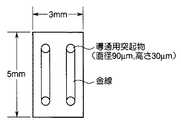
評価用のチップとしては、図7に示す大きさが3mm×5mmで、直径90μm、高さ30μmの金製バンプ(導通用突起物)が4つ設けられた評価用ダミーチップを用いる。バンプは、2つが一組となり、金線で導通がとられている。したがって、ウエハには、上記のチップに対応するダミー回路が多数設けられている。
【0045】
またチップ搭載用基板としては、図8に示す上記バンプの位置に対応する配線パターンを有する基板を評価用基板として用いる。
【0046】
【実施例1】
バインダー樹脂としてアクリル樹脂10重量部と、ウレタン系アクリレートオリゴマー10重量部と、2,2-ジメトキシ-2-フェニルアセトン0.3重量部と、エポキシ樹脂105重量部と、ジシアンジアミド2.12重量部と、アクリル系ゴム微粒子5重量部と、芳香族系ポリイソシアナート2重量部とからなる粘接着剤組成物を、剥離性シートとして表面張力35 mN/mのポリエチレンフィルム(厚さ:100μm)に塗布・乾燥し、厚さ60μmの絶縁性粘接着剤層を有する粘接着テープを得、これを剥離性シートを有する絶縁性接着性薄膜層とした。
【0047】
前記した回路パターンを有する半導体ウエハ(6インチ、厚さ625μm)の回路面に、上記接着性薄膜層を常温で圧着(テープ貼付装置:リンテック社製、Adwill RAD-3500使用)した。半導体ウエハ裏面を研削(研削装置:ディスコ社製、DFG-840使用)して、厚さを300μmにし、その後研削面にダイシングテープ(Adwill G-19、リンテック社製)を貼付後、ダイシング装置(ディスコ社製、DAD-2H/6T)を使用して回路パターン毎に切断分離し、チップを得た。
【0048】
回路面側に紫外線照射(紫外線照射装置:リンテック社製、Adwill RAD 2000m/6使用)を行い、次いで、接着性薄膜層上の剥離性シート上に強粘着テープを貼付し、これを剥離することで、接着性薄膜層上の剥離性シートを剥離し、チップの回路面に接着性薄膜層を残存させた。得られたチップをピックアップし、チップトレーに収納した。
【0049】
次いでフリップチップボンダー(九州松下電器産業(株)製、FB30T-M)を用い、前記評価用基板に実装した。実装の際の、ステージ温度は60℃、ヘッド温度は180℃、荷重は20N、時間は60秒とした。
実装後、150℃のオーブン中で60分保持し、粘接着剤層を完全に硬化させた。各端子間の抵抗値を、低抵抗率計(三菱化学製、Loresta-GP MCP-T600)を用いて測定し、ab間およびcd間の導通と、その他の端子間の絶縁を確認した。
【0050】
[参考例2]
アクリル樹脂10重量部と、エポキシ樹脂80重量部と、ジシアンジアミド2重量部とからなる粘接着剤組成物に、平均粒径6〜10μmのフレーク状銀粉を、樹脂固形分100重量部に対し、10重量部加え、異方導電性粘接着剤組成物を得た。得られた粘接着剤組成物を、剥離性シートとして表面張力35 mN/mのポリエチレンフィルム(厚さ:100μm)に塗布・乾燥し、厚さ40μmの異方導電性の粘接着剤層を有する粘接着テープを得、これを剥離性シートを有する接着性薄膜層とした。
【0051】
実施例1と同様にして、前記した回路パターンを有する半導体ウエハ(6インチ、厚さ625μm)の回路面に、上記接着性薄膜層を常温で圧着した。また実施例1と同様にして、半導体ウエハ裏面を研削して、厚さを300μmにし、その後研削面にダイシングテープを貼付後、回路パターン毎に切断分離し、チップを得た。次いで、粘接着テープのポリエチレンフィルム上に強粘着テープを貼付し、これを剥離することで、粘接着テープのポリエチレンフィルムを剥離し、チップの回路面に粘接着剤層を残存させた。チップをピックアップし、チップトレーに収納した。
【0052】
次いでフリップチップボンダーを用い、前記評価用基板に実装した。実装の際の、ステージ温度は60℃、ヘッド温度は130℃、荷重は20N、時間は60秒とした。
実装後、150℃のオーブン中で60分保持し、粘接着剤層を完全に硬化させた。各端子間の抵抗値を、低抵抗率計を用いて測定し、ab間およびcd間の導通と、その他の端子間の絶縁を確認した。
【0053】
【実施例3】
剥離性シートとしてアルキッド系剥離剤により剥離処理したポリエチレンナフタレートフィルム(厚さ25μm:融点272℃:表面張力34mN/m)の処理面に熱可塑性ポリイミド樹脂(Tg=115℃:宇部興産社製)からなる接着剤を塗布後、乾燥し、厚さ60μmの絶縁性接着剤からなる接着性薄膜層を有するシートを作成した。
【0054】
実施例1と同様にして、前記した回路パターンを有する半導体ウエハ(6インチ、厚さ625μm)の回路面に、上記接着性薄膜層を常温で圧着した。また実施例1と同様にして、半導体ウエハ裏面を研削して、厚さを300μmにし、その後研削面にダイシングテープを貼付後、回路パターン毎に切断分離し、チップを得た。
次いで、接着性薄膜層上のポリエチレンナフタレートフィルム上に強粘着テープを貼付し、これを剥離することで、接着性薄膜層上のポリエチレンナフタレートフィルムを剥離し、チップの回路面に接着性薄膜層を残存させた。得られたチップをピックアップし、チップトレーに収納した。
【0055】
次いでフリップチップボンダーを用い、前記評価用基板に実装した。実装の際の、ステージ温度は150℃、ヘッド温度は180℃、荷重は20N、時間は60秒とした。
各端子間の抵抗値を、低抵抗率計を用いて測定し、ab間およびcd間の導通と、その他の端子間の絶縁を確認した。
【0056】
【実施例4】
常温で固型のエポキシ樹脂(エポキシ当量3000〜5000)90重量部と、常温で液状のエポキシ樹脂(エポキシ当量184〜194)10重量部と、ジシアンジアミド2重量部とからなる接着剤組成物を、溶剤で希釈した状態で、実施例3で用いた剥離性シートに塗布後、乾燥し、厚さ60μmの絶縁性の接着性薄膜層を有するシートを作成した。
【0057】
実施例1と同様にして、前記した回路パターンを有する半導体ウエハ(6インチ、厚さ625μm)の回路面に、上記接着性薄膜層を常温で圧着した。また実施例1と同様にして、半導体ウエハ裏面を研削して、厚さを300μmにし、その後研削面にダイシングテープを貼付後、回路パターン毎に切断分離し、チップを得た。
次いで、接着性薄膜層上のポリエチレンナフタレートフィルム上に強粘着テープを貼付し、これを剥離することで、接着性薄膜上のポリエチレンナフタレートフィルムを剥離し、チップの回路面に接着性薄膜を残存させた。得られたチップをピックアップし、チップトレーに収納した。
【0058】
次いでフリップチップボンダーを用い、前記評価用基板に実装した。実装の際の、ステージ温度は60℃、ヘッド温度は130℃、荷重は20N、時間は60秒とした。
実装後、150℃のオーブン中で60分保持し、粘接着剤層を完全に硬化させた。各端子間の抵抗値を、低抵抗率計を用いて測定し、ab間およびcd間の導通と、その他の端子間の絶縁を確認した。
【図面の簡単な説明】
【図1】 本発明に係る製造方法の工程の概略を示す。
【図2】 本発明に係る製造方法の工程の概略を示す。
【図3】 本発明に係る製造方法の工程の概略を示す。
【図4】 本発明に係る他の製造方法の工程の概略を示す。
【図5】 本発明に係る他の製造方法の工程の概略を示す。
【図6】 本発明に係る他の製造方法の工程の概略を示す。
【図7】 本発明の実施例で用いた評価用チップの平面図を示す。
【図8】 本発明の実施例で用いた評価用基板の平面図を示す。
【符号の説明】
1…半導体ウエハ、2…チップ、11…剥離性シート、
12…接着性薄膜層(異方導電性接着剤層)、
21…剥離性シート、
22…接着性薄膜層(絶縁性接着剤層)、
30…チップ搭載用基板、
31,31’…導通用突起物[0001]
BACKGROUND OF THE INVENTION
The present invention relates to a method for manufacturing a semiconductor device, and more particularly to a method capable of efficiently producing a highly reliable product by preventing generation of voids when manufacturing a resin-encapsulated semiconductor device.
[0002]
[Prior art]
Generally, a semiconductor device is sealed with a resin in order to protect a circuit surface. Conventionally, such a resin-sealed semiconductor device is manufactured by individually mounting each IC chip on a lead frame and then sealing each one with a mold.
[0003]
More specifically, the following methods are currently being used.
(1) The IC chip and the lead frame are connected using a gold wire or the like, and then sealed with resin.
(2) The IC chip is placed on the lead frame on which the conductive protrusion is formed, the IC chip and the lead frame are connected via the conductive protrusion, and then sealed with resin.
(3) The IC chip and the lead frame are connected via an anisotropic conductive film or anisotropic conductive paste, and then sealed with resin.
[0004]
However, in the above method (1), since the gold wire must be molded, the semiconductor device is too large compared to the chip size, and there is a problem that it is difficult to use in a small device such as a mobile phone. For this reason, the method (2) or (3) has been used in which the size of the semiconductor device can be made substantially equal to the chip size.
[0005]
However, in the method (2), there is a space between the IC chip and the lead frame by the height of the conductive protrusion, and even if resin sealing is performed, the resin is sufficiently in this space. Voids may occur without entering. For this reason, it is necessary to fill an insulating adhesive between the IC chip and the lead frame before resin sealing.
[0006]
In the method (3), it is necessary to attach an anisotropic conductive film or apply an anisotropic conductive paste to a minute IC chip, which is also complicated in terms of work steps. In particular, it is difficult to apply a certain amount of anisotropic conductive paste, and the amount of paste differs from product to product, which may cause variations in product characteristics.
[0007]
[Problems to be solved by the invention]
The present invention has been made in view of the prior art as described above, and provides a method capable of efficiently producing a highly reliable product by preventing generation of voids during the manufacture of a resin-encapsulated semiconductor device. The purpose is to do.
[0008]
[Means for Solving the Problems]
A method for manufacturing a semiconductor device according to the present invention includes:
An adhesive thin film layer is formed on the circuit surface of a semiconductor wafer having a circuit formed on the surface,
The semiconductor wafer is cut and separated into individual chips for each circuit,
The individual chip is placed at a predetermined position on the chip mounting substrate via the adhesive thin film layer,
The individual chip is bonded and fixed to the chip mounting substrate while ensuring conduction between the individual chip and the chip mounting substrate.
[0009]
In the present invention, before the semiconductor wafer is cut and separated into individual chips, the back surface of the semiconductor wafer may be ground while protecting the circuit surface of the semiconductor wafer with the adhesive thin film layer.
The adhesive thin film layer has a peelable sheet on one side, and the adhesive thin film layer is attached to the circuit surface of the semiconductor wafer via the surface of the adhesive thin film layer on which the peelable sheet is not formed. By forming an adhesive thin film layer on the circuit surface of the semiconductor wafer,
Before the individual chip is placed on the chip mounting substrate, the peelable sheet can be peeled from the adhesive thin film layer.
[0010]
Furthermore, in the present invention, the adhesive thin film layer may be formed of an anisotropic conductive adhesive.
Further, the adhesive thin film layer may be made of an insulating adhesive. In this case, the adhesive thin film layer having a conductive projection on the circuit of the chip and / or the chip mounting substrate is used for the adhesion. The thin film layer can be fluidized by heating to ensure conduction between the chip and the chip mounting substrate via the conduction protrusion.
[0011]
According to such a method for manufacturing a semiconductor device according to the present invention, voids can be prevented from being generated during the manufacture of a resin-encapsulated semiconductor device, and a highly reliable product can be efficiently manufactured.
[0012]
DETAILED DESCRIPTION OF THE INVENTION
Hereinafter, the present invention will be described more specifically with reference to the drawings.
In the first method for manufacturing a semiconductor device according to the present invention, first, as shown in FIG.
An adhesive thin film layer 12 (or 22) is formed on the circuit surface of the
[0013]
Examples of the
Formation of a circuit on the wafer surface can be performed by various methods including conventionally used methods such as an etching method and a lift-off method. In the semiconductor wafer circuit forming step, a predetermined circuit is formed.
[0014]
In this circuit formation step, an oxide film may be formed on the back surface of the wafer. Such an oxide film is removed by grinding the back surface of the wafer, which will be described later, if necessary.
The adhesive thin film layer is made of an anisotropic conductive adhesive or an insulating adhesive.
The adhesive
[0015]
As a material used as the binder resin, a resin used as a normal adhesive is not particularly limited, and may be a thermosetting material or a thermoplastic material. Moreover, you may use what is called an adhesive which is pressure-sensitive adhesiveness at the time of sticking, and hardens | cures by heating later.
As the thermosetting binder resin, for example, an epoxy resin, an acrylic resin, a polyimide resin, a phenol resin, a urea resin, a melamine resin, a resorcinol resin, or the like is used, and an epoxy resin or an acrylic resin is preferably used.
[0016]
Examples of the thermoplastic binder resin include polyester resin, polyvinyl acetate, polyvinyl alcohol, polyvinyl butyral, polyvinyl chloride, polymethacrylate, polyacrylate, polystyrene, polyethylene, polyamide, cellulose, polyisobutylene, polyvinyl ether, polyimide resin, and various types. Hot-melt adhesives are preferably used, and polyester resins and polyimide resins are preferably used.
[0017]
Examples of the adhesive include a mixture of a binder resin having a pressure-sensitive adhesive property at room temperature and a thermosetting resin. Examples of the binder resin having pressure-sensitive adhesive properties at room temperature include acrylic resins, polyester resins, polyvinyl ethers, urethane resins, and polyamides. Examples of the thermosetting resin include the same resins as the above-mentioned thermosetting binder resin, and those having a relatively low molecular weight than the binder resin can be used. Moreover, it is preferable to mix | blend ultraviolet curable resin, such as a urethane type acrylate oligomer, in order to control peelability with the peelable sheet mentioned later to an adhesive agent. When an ultraviolet curable resin is blended, the peelable sheet adheres well to the adhesive thin film layer before the ultraviolet irradiation, and is easily peeled after the ultraviolet irradiation.
[0018]
Materials used as the conductive particles include powders of metal or alloys such as gold, silver, copper, nickel and aluminum, fibrous bodies, carbon black, conductive polymer powders such as polyaniline and polypyrrole, and fibers. The body is used. These materials may be used alone or in combination of two or more. Further, the shape of the powder or the like may be formed of a conductive material alone, or may be coated or plated on a resin such as styrene or acrylic. The size of the powder or fibrous body is preferably about 1 to 20 μm.
[0019]
Such conductive particles are used at a ratio of about 1 to 500 parts by weight with respect to 100 parts by weight of the binder resin.
The film thickness of the anisotropic conductive
The adhesive
[0020]
The insulating adhesive is the same as the anisotropic conductive adhesive except that it does not contain conductive particles, and may be thermosetting, thermoplastic, or adhesive. It may consist of a dressing.
That is, the thermosetting insulating
The thermoplastic insulating
[0021]
Further, the adhesive
The film thickness of the insulating
In the present invention, as shown in FIG. 1 or FIG. 4, the
[0022]
The adhesive thin film layer is used by laminating a peelable sheet in a predetermined process, and then transferred from the peelable sheet to a wafer or a chip. The peelable sheet is used for reinforcement so as not to be deformed by tension, for example, when an adhesive thin film layer is stuck to a wafer. In addition, the surface of the adhesive thin film layer can be protected during the grinding process or the cutting and separating process.
[0023]
As the peelable sheet, various thin layer products conventionally used as substrates such as pressure-sensitive adhesive tapes are used without particular limitation, for example, paper, metal foil, polyethylene terephthalate, polyethylene, polystyrene, polypropylene, Synthetic resin films such as nylon, urethane, polyvinylidene chloride, and polyvinyl chloride are used. Moreover, these laminated products may be sufficient.
[0024]
In the present invention, in order to peel the adhesive thin film layer from the surface of the peelable sheet and facilitate transfer to a chip or the like, the surface of the peelable sheet is subjected to a release treatment with a silicone resin or an alkyd resin as necessary. You may give it.
The surface tension of the
[0025]
When the surface tension of the peelable sheet is greater than 40 mN / m, the adhesive thin film layer has high adhesion to the peelable sheet, and transfer to the chip body may not be possible. On the other hand, if it is less than 20 mN / m, the grinding water may enter between the peelable sheet and the adhesive thin film layer during the grinding process and damage the wafer. Depending on the properties of the adhesive thin film layer, the adhesive may adhere to the peelable sheet. May not be formed.
[0026]
The thickness of the
In the method for manufacturing a semiconductor device of the present invention, an adhesive thin film forming step, a cutting and separating step, and a chip bonding and fixing step are performed. Moreover, a back grinding process may be performed if desired.
[0027]
The adhesive
[0028]
The sticking temperature depends on the properties of the adhesive thin film layer used. Usually, a temperature not lower than the plasticization temperature of the binder resin and not higher than 180 ° C. is preferred. In addition, when an adhesive is used, it can be stuck at room temperature. If the sticking temperature is too high, the wafer may be warped after grinding. In addition, when the unevenness of the circuit surface of the wafer is large so that the height of the conductive projection provided on the circuit surface of the wafer is 50 μm or more, the application is performed under conditions stronger than the standard pressure condition or at a higher application temperature. The wafer circuit surface is preferably in close contact.
[0029]
In the present invention, various required processes such as cutting and separation of the
The back surface grinding step of the
[0030]
Next, the wafer is cut and separated. Wafer cutting and separation are performed using a normal dicing apparatus. At this time, dicing tape is attached to the back surface of the wafer, and the dicing tape is fixed to the circular frame via the dicing tape.
Subsequently, the chips cut and separated using a pickup device or a chip bonder are individually collected in a chip tray or the like.
[0031]
Through such a required process, a
In the present invention, the adhesive thin film layer, when using a peelable sheet, after applying the composition of the adhesive on the peelable surface of the peelable sheet and drying as necessary, or cast into a thin film, It is formed by laminating peelable sheets. Moreover, when not using a peelable sheet, it manufactures by cast shaping | molding etc.
[0032]
In the case where a peelable sheet is laminated on the adhesive thin film layer, the peelable sheet is peeled from the adhesive thin film layer before placing the cut and separated individual chips on the chip mounting substrate.
As a method for peeling the peelable sheet from the adhesive thin film layer, a wide adhesive sheet is attached to the entire surface of the peelable sheet and then peeled off at an acute angle. Peeling of the peelable sheet is preferably performed after cutting and separation, but may be performed before cutting and separation.
[0033]
Next, in the method of manufacturing a semiconductor device according to the present invention, the
A predetermined circuit is formed on the surface of the
[0034]
The
[0035]
When the adhesive thin film layer is made of an anisotropic conductive adhesive, the
[0036]
In the case where the anisotropic conductive
Further, when the anisotropic conductive
[0037]
When the adhesive
[0038]
In this case, the
[0039]
When the insulating
[0040]
Further, when the insulating
[0041]
Bonding and fixing of the
According to such a method for manufacturing a semiconductor device according to the present invention, the
[0042]
As the resin used for resin sealing, various thermosetting resins conventionally used for resin sealing of semiconductor devices are used.
Specific examples of such thermosetting resins include cresol novolac-type epoxy, naphthalene-type epoxy, biphenyl-type epoxy or aromatic polyfunctional type epoxy as main raw materials, and commonly used curing agents such as phenol novolac and silica. A resin in which silicone, carbon, filler and the like are mixed is preferably used. The conditions for heat curing are appropriately determined according to the type of thermosetting resin used.
[0043]
【The invention's effect】
According to the method for manufacturing a semiconductor device according to the present invention, generation of voids can be prevented and a highly reliable product can be efficiently manufactured at the time of manufacturing a resin-encapsulated semiconductor device.
[0044]
【Example】
EXAMPLES The present invention will be described below with reference to examples, but the present invention is not limited to these examples.
The conduction evaluation of the semiconductor device was performed as follows.
As an evaluation chip, an evaluation dummy chip provided with four gold bumps (conduction protrusions) having a size of 3 mm × 5 mm, a diameter of 90 μm, and a height of 30 μm shown in FIG. 7 is used. Two bumps are paired and are electrically connected by a gold wire. Therefore, a large number of dummy circuits corresponding to the above chips are provided on the wafer.
[0045]
As the chip mounting substrate, a substrate having a wiring pattern corresponding to the position of the bump shown in FIG. 8 is used as the evaluation substrate.
[0046]
[Example 1]
As binder resin, 10 parts by weight of acrylic resin, 10 parts by weight of urethane acrylate oligomer, 0.3 part by weight of 2,2-dimethoxy-2-phenylacetone, 105 parts by weight of epoxy resin, 2.12 parts by weight of dicyandiamide An adhesive composition consisting of 5 parts by weight of acrylic rubber fine particles and 2 parts by weight of aromatic polyisocyanate is applied to a polyethylene film (thickness: 100 μm) having a surface tension of 35 mN / m as a peelable sheet. Application and drying were performed to obtain an adhesive tape having an insulating adhesive layer having a thickness of 60 μm, and this was used as an insulating adhesive thin film layer having a peelable sheet.
[0047]
The above-mentioned adhesive thin film layer was pressure-bonded to the circuit surface of a semiconductor wafer (6 inches, thickness 625 μm) having the circuit pattern described above at room temperature (tape application device: manufactured by Lintec Corporation, using Adwill RAD-3500). Grind the backside of the semiconductor wafer (grinding device: manufactured by DISCO, using DFG-840) to a thickness of 300 μm, and then apply dicing tape (Adwill G-19, manufactured by Lintec) on the ground surface, then dicing device ( A chip was obtained by cutting and separating each circuit pattern using DAD-2H / 6T.
[0048]
Irradiate the circuit surface with ultraviolet rays (ultraviolet irradiation device: manufactured by Lintec, Adwill RAD 2000m / 6), and then apply a strong adhesive tape on the peelable sheet on the adhesive thin film layer and peel it off Then, the peelable sheet on the adhesive thin film layer was peeled off, and the adhesive thin film layer was left on the circuit surface of the chip. The obtained chip was picked up and stored in a chip tray.
[0049]
Subsequently, it mounted on the said board | substrate for evaluation using the flip chip bonder (Kyushu Matsushita Electric Industrial Co., Ltd. product, FB30T-M). During mounting, the stage temperature was 60 ° C., the head temperature was 180 ° C., the load was 20 N, and the time was 60 seconds.
After mounting, it was kept in an oven at 150 ° C. for 60 minutes to completely cure the adhesive layer. The resistance value between each terminal was measured using a low resistivity meter (Mitsubishi Chemical, Loresta-GP MCP-T600), and conduction between ab and cd and insulation between other terminals were confirmed.
[0050]
[Reference example2]
To an adhesive composition comprising 10 parts by weight of an acrylic resin, 80 parts by weight of an epoxy resin, and 2 parts by weight of dicyandiamide, flaky silver powder having an average particle size of 6 to 10 μm is added to 100 parts by weight of the resin solid content. 10 parts by weight was added to obtain an anisotropic conductive adhesive composition. The obtained adhesive composition is applied to a polyethylene film (thickness: 100 μm) having a surface tension of 35 mN / m as a peelable sheet and dried, and an anisotropic conductive adhesive layer having a thickness of 40 μm. The adhesive tape which has this was obtained and this was made into the adhesive thin film layer which has a peelable sheet.
[0051]
In the same manner as in Example 1, the adhesive thin film layer was pressure-bonded to the circuit surface of a semiconductor wafer (6 inches, thickness 625 μm) having the circuit pattern described above at room temperature. In the same manner as in Example 1, the back surface of the semiconductor wafer was ground to a thickness of 300 μm, and then a dicing tape was applied to the ground surface, and then cut and separated for each circuit pattern to obtain a chip. Next, a strong adhesive tape was affixed onto the polyethylene film of the adhesive tape, and the adhesive film was peeled off to release the polyethylene film of the adhesive tape, leaving the adhesive layer on the circuit surface of the chip. . Chips were picked up and stored in a chip tray.
[0052]
Subsequently, it mounted on the said board | substrate for evaluation using the flip chip bonder. During mounting, the stage temperature was 60 ° C., the head temperature was 130 ° C., the load was 20 N, and the time was 60 seconds.
After mounting, it was kept in an oven at 150 ° C. for 60 minutes to completely cure the adhesive layer. The resistance value between each terminal was measured using the low resistivity meter, and conduction | electrical_connection between ab and cd and the insulation between other terminals were confirmed.
[0053]
[Example 3]
Thermoplastic polyimide resin (Tg = 115 ° C: manufactured by Ube Industries) on the treated surface of a polyethylene naphthalate film (thickness 25 μm: melting point 272 ° C .: surface tension 34 mN / m) peel-treated with an alkyd-type release agent as a release sheet After applying the adhesive composed of the above, it was dried to prepare a sheet having an adhesive thin film layer composed of an insulating adhesive having a thickness of 60 μm.
[0054]
In the same manner as in Example 1, the adhesive thin film layer was pressure-bonded to the circuit surface of a semiconductor wafer (6 inches, thickness 625 μm) having the circuit pattern described above at room temperature. In the same manner as in Example 1, the back surface of the semiconductor wafer was ground to a thickness of 300 μm, and then a dicing tape was applied to the ground surface, and then cut and separated for each circuit pattern to obtain a chip.
Next, a strong adhesive tape is applied to the polyethylene naphthalate film on the adhesive thin film layer, and the polyethylene naphthalate film on the adhesive thin film layer is peeled off by peeling off the adhesive tape. The layer was left. The obtained chip was picked up and stored in a chip tray.
[0055]
Subsequently, it mounted on the said board | substrate for evaluation using the flip chip bonder. During mounting, the stage temperature was 150 ° C., the head temperature was 180 ° C., the load was 20 N, and the time was 60 seconds.
The resistance value between each terminal was measured using the low resistivity meter, and conduction | electrical_connection between ab and cd and the insulation between other terminals were confirmed.
[0056]
[Example 4]
An adhesive composition comprising 90 parts by weight of a solid epoxy resin (epoxy equivalent 3000 to 5000) at normal temperature, 10 parts by weight of an epoxy resin liquid (epoxy equivalent 184 to 194) at normal temperature, and 2 parts by weight of dicyandiamide, In a state diluted with a solvent, the sheet was applied to the peelable sheet used in Example 3 and then dried to prepare a sheet having an insulating adhesive thin film layer having a thickness of 60 μm.
[0057]
In the same manner as in Example 1, the adhesive thin film layer was pressure-bonded to the circuit surface of a semiconductor wafer (6 inches, thickness 625 μm) having the circuit pattern described above at room temperature. In the same manner as in Example 1, the back surface of the semiconductor wafer was ground to a thickness of 300 μm, and then a dicing tape was applied to the ground surface, and then cut and separated for each circuit pattern to obtain a chip.
Next, a strong adhesive tape is affixed on the polyethylene naphthalate film on the adhesive thin film layer and peeled off to peel off the polyethylene naphthalate film on the adhesive thin film, and the adhesive thin film is applied to the circuit surface of the chip. Remained. The obtained chip was picked up and stored in a chip tray.
[0058]
Subsequently, it mounted on the said board | substrate for evaluation using the flip chip bonder. During mounting, the stage temperature was 60 ° C., the head temperature was 130 ° C., the load was 20 N, and the time was 60 seconds.
After mounting, it was kept in an oven at 150 ° C. for 60 minutes to completely cure the adhesive layer. The resistance value between each terminal was measured using the low resistivity meter, and conduction | electrical_connection between ab and cd and the insulation between other terminals were confirmed.
[Brief description of the drawings]
FIG. 1 shows an outline of the steps of a production method according to the present invention.
FIG. 2 shows an outline of the steps of the production method according to the present invention.
FIG. 3 shows an outline of the steps of the production method according to the present invention.
FIG. 4 shows an outline of the steps of another manufacturing method according to the present invention.
FIG. 5 shows an outline of the steps of another manufacturing method according to the present invention.
FIG. 6 shows an outline of steps of another manufacturing method according to the present invention.
FIG. 7 is a plan view of an evaluation chip used in an example of the present invention.
FIG. 8 is a plan view of an evaluation substrate used in an example of the present invention.
[Explanation of symbols]
DESCRIPTION OF
12 ... adhesive thin film layer (anisotropic conductive adhesive layer),
21 ... peelable sheet,
22: Adhesive thin film layer (insulating adhesive layer),
30 ... Chip mounting substrate,
31, 31 '... conductive protrusion
Claims (1)
Translated fromJapanese該接着性薄膜層により半導体ウエハの回路面を保護しながら該半導体ウエハの裏面を研削し、
次いで該半導体ウエハを、回路毎に個別のチップに切断分離し、
次いで、該剥離性シートを該接着性薄膜層から剥離し、該個別のチップを該接着性薄膜層を介して、チップ搭載用基板の所定位置に載置し、
該個別のチップと該チップ搭載用基板との導通を確保しながら該個別のチップを該チップ搭載用基板に接着固定し、
該チップの回路上および/またはチップ搭載用基板上には導通用突起物が有り、該接着性薄膜層を加熱により流動化させて該導通用突起物を介してチップとチップ搭載用基板との間に導通を確保することを特徴とする半導体装置の製造方法。A semiconductor waferhaving a peelable sheet on one side and a circuit formed on the surface of the adhesive thin film layerthrough the surface on which the peelable sheet of the adhesive thin film layer made of an insulating adhesive is not formed By adhering to the circuit surface,an adhesive thin film layerin which a release sheet is laminated is formed on the circuit surface of the semiconductor wafer,
Grinding the back surface of the semiconductor wafer while protecting the circuit surface of the semiconductor wafer by the adhesive thin film layer;
Next, the semiconductor wafer is cut and separated into individual chips for each circuit,
Next, the peelable sheet is peeled from the adhesive thin film layer, and the individual chips are placed at predetermined positions on the chip mounting substrate via the adhesive thin film layer,
Adhering and fixing the individual chip to the chip mounting substrate while ensuring conduction between the individual chip and the chip mounting substrate,
There are conductive protrusions on the circuit of the chip and / or on the chip mounting substrate, and the adhesive thin film layer is fluidized by heating, and the chip and the chip mounting substrate are connected via the conductive protrusions. A method for manufacturing a semiconductor device, whereinconduction is ensured between them .
Priority Applications (1)
| Application Number | Priority Date | Filing Date | Title |
|---|---|---|---|
| JP32190399AJP4180206B2 (en) | 1999-11-12 | 1999-11-12 | Manufacturing method of semiconductor device |
Applications Claiming Priority (1)
| Application Number | Priority Date | Filing Date | Title |
|---|---|---|---|
| JP32190399AJP4180206B2 (en) | 1999-11-12 | 1999-11-12 | Manufacturing method of semiconductor device |
Publications (2)
| Publication Number | Publication Date |
|---|---|
| JP2001144140A JP2001144140A (en) | 2001-05-25 |
| JP4180206B2true JP4180206B2 (en) | 2008-11-12 |
Family
ID=18137703
Family Applications (1)
| Application Number | Title | Priority Date | Filing Date |
|---|---|---|---|
| JP32190399AExpired - LifetimeJP4180206B2 (en) | 1999-11-12 | 1999-11-12 | Manufacturing method of semiconductor device |
Country Status (1)
| Country | Link |
|---|---|
| JP (1) | JP4180206B2 (en) |
Cited By (1)
| Publication number | Priority date | Publication date | Assignee | Title |
|---|---|---|---|---|
| CN112219268A (en)* | 2018-06-29 | 2021-01-12 | 琳得科株式会社 | installation method |
Families Citing this family (22)
| Publication number | Priority date | Publication date | Assignee | Title |
|---|---|---|---|---|
| JP2001237268A (en)* | 2000-02-22 | 2001-08-31 | Nec Corp | Method for mounting semiconductor element and apparatus for manufacturing the same |
| JP4659300B2 (en) | 2000-09-13 | 2011-03-30 | 浜松ホトニクス株式会社 | Laser processing method and semiconductor chip manufacturing method |
| TWI326626B (en) | 2002-03-12 | 2010-07-01 | Hamamatsu Photonics Kk | Laser processing method |
| JP4358502B2 (en)* | 2002-03-12 | 2009-11-04 | 浜松ホトニクス株式会社 | Semiconductor substrate cutting method |
| WO2003076119A1 (en) | 2002-03-12 | 2003-09-18 | Hamamatsu Photonics K.K. | Method of cutting processed object |
| EP2400539B1 (en) | 2002-03-12 | 2017-07-26 | Hamamatsu Photonics K.K. | Substrate dividing method |
| TWI520269B (en) | 2002-12-03 | 2016-02-01 | Hamamatsu Photonics Kk | Cutting method of semiconductor substrate |
| DE60315515T2 (en) | 2003-03-12 | 2007-12-13 | Hamamatsu Photonics K.K., Hamamatsu | LASER PROCESSING PROCEDURES |
| JP4170839B2 (en) | 2003-07-11 | 2008-10-22 | 日東電工株式会社 | Laminated sheet |
| JP2005064239A (en) | 2003-08-12 | 2005-03-10 | Lintec Corp | Manufacturing method of semiconductor device |
| JP5428135B2 (en)* | 2006-04-05 | 2014-02-26 | 日立化成株式会社 | Laminate and method for producing the same |
| JP2010528450A (en)* | 2007-02-09 | 2010-08-19 | エルジー イノテック カンパニー リミテッド | Multifunctional die adhesive film and semiconductor element packaging method using the same |
| KR100963675B1 (en)* | 2008-03-14 | 2010-06-15 | 제일모직주식회사 | Multifunctional tape for semiconductor packaging and manufacturing method of semiconductor device using same |
| JP5436827B2 (en)* | 2008-03-21 | 2014-03-05 | 日立化成株式会社 | Manufacturing method of semiconductor device |
| JP5040804B2 (en)* | 2008-05-16 | 2012-10-03 | 日本電気株式会社 | Semiconductor device manufacturing method and semiconductor element inspection structure |
| JP5525200B2 (en)* | 2008-07-28 | 2014-06-18 | 積水化学工業株式会社 | Manufacturing method of semiconductor chip laminated body |
| JP5476033B2 (en)* | 2009-04-24 | 2014-04-23 | 積水化学工業株式会社 | Mounting method of semiconductor chip |
| JP2010258239A (en)* | 2009-04-24 | 2010-11-11 | Sekisui Chem Co Ltd | Insulating adhesive sheet |
| JP5395701B2 (en)* | 2010-02-19 | 2014-01-22 | 積水化学工業株式会社 | Adhesive sheet substrate, adhesive sheet and semiconductor chip mounting method |
| TWI430376B (en)* | 2011-02-25 | 2014-03-11 | The Method of Fabrication of Semiconductor Packaging Structure | |
| JP2013197557A (en)* | 2012-03-23 | 2013-09-30 | Sumitomo Bakelite Co Ltd | Method of measuring potential of semiconductor element |
| JP6271463B2 (en) | 2015-03-11 | 2018-01-31 | 東芝メモリ株式会社 | Semiconductor device |
- 1999
- 1999-11-12JPJP32190399Apatent/JP4180206B2/ennot_activeExpired - Lifetime
Cited By (2)
| Publication number | Priority date | Publication date | Assignee | Title |
|---|---|---|---|---|
| CN112219268A (en)* | 2018-06-29 | 2021-01-12 | 琳得科株式会社 | installation method |
| US20210111036A1 (en)* | 2018-06-29 | 2021-04-15 | Lintec Corporation | Mounting method of work |
Also Published As
| Publication number | Publication date |
|---|---|
| JP2001144140A (en) | 2001-05-25 |
Similar Documents
| Publication | Publication Date | Title |
|---|---|---|
| JP4180206B2 (en) | Manufacturing method of semiconductor device | |
| TWI696681B (en) | Film-shaped adhesive and method for manufacturing semiconductor package using film-shaped adhesive | |
| CN1333462C (en) | Laminated sheet | |
| CN105339450B (en) | Protective tape and method for manufacturing semiconductor device using the same | |
| EP1248291B1 (en) | Adhesive sheet with conductor bodies for flip-chip mounting | |
| KR101140512B1 (en) | Thermosetting die bonding film | |
| JP6033734B2 (en) | Film adhesive, dicing tape integrated film adhesive, and method for manufacturing semiconductor device | |
| KR102276498B1 (en) | Method of manufacturing semiconductor device, and semiconductor device | |
| US7169648B2 (en) | Process for producing a semiconductor device | |
| JPH10107048A (en) | Multichip mounting method, adhesive-applied chip set, and manufacture of adhesive-applied chip | |
| US7132755B2 (en) | Adhesive film for manufacturing semiconductor device | |
| JP5710098B2 (en) | Manufacturing method of semiconductor device | |
| JPH09505444A (en) | Multi-chip electronic package module using adhesive sheet | |
| KR20170020277A (en) | Method for manufacturing semiconductor device and semiconductor device | |
| JP2008098427A (en) | Manufacturing method of semiconductor device | |
| CN107614641B (en) | Semiconductor processing belt | |
| JP4271544B2 (en) | Manufacturing method of semiconductor device | |
| JP3961672B2 (en) | Manufacturing method of resin-encapsulated chip body | |
| US9153556B2 (en) | Adhesive sheet for manufacturing semiconductor device, manufacturing method of semiconductor device using the sheet, and semiconductor device obtained by the method | |
| JP2006318999A (en) | Adhesive film for semiconductor device manufacturing | |
| JP2018098228A (en) | Protection tape, and method for manufacturing semiconductor device by use thereof | |
| CN113474433A (en) | Film-like adhesive, adhesive sheet and semiconductor device | |
| JP2001144120A (en) | Semiconductor device and method of manufacturing the same | |
| WO2022149581A1 (en) | Adhesive agent composition, film-form adhesive agent, dicing/die-bonding integrated film, semiconductor device, and method for manufacturing same | |
| JPS62285429A (en) | Manufacture of semiconductor device |
Legal Events
| Date | Code | Title | Description |
|---|---|---|---|
| A621 | Written request for application examination | Free format text:JAPANESE INTERMEDIATE CODE: A621 Effective date:20060728 | |
| A977 | Report on retrieval | Free format text:JAPANESE INTERMEDIATE CODE: A971007 Effective date:20080425 | |
| A131 | Notification of reasons for refusal | Free format text:JAPANESE INTERMEDIATE CODE: A131 Effective date:20080513 | |
| A521 | Written amendment | Free format text:JAPANESE INTERMEDIATE CODE: A523 Effective date:20080711 | |
| TRDD | Decision of grant or rejection written | ||
| A01 | Written decision to grant a patent or to grant a registration (utility model) | Free format text:JAPANESE INTERMEDIATE CODE: A01 Effective date:20080805 | |
| A01 | Written decision to grant a patent or to grant a registration (utility model) | Free format text:JAPANESE INTERMEDIATE CODE: A01 | |
| A61 | First payment of annual fees (during grant procedure) | Free format text:JAPANESE INTERMEDIATE CODE: A61 Effective date:20080827 | |
| R150 | Certificate of patent or registration of utility model | Free format text:JAPANESE INTERMEDIATE CODE: R150 Ref document number:4180206 Country of ref document:JP Free format text:JAPANESE INTERMEDIATE CODE: R150 | |
| FPAY | Renewal fee payment (event date is renewal date of database) | Free format text:PAYMENT UNTIL: 20110905 Year of fee payment:3 | |
| FPAY | Renewal fee payment (event date is renewal date of database) | Free format text:PAYMENT UNTIL: 20120905 Year of fee payment:4 | |
| R250 | Receipt of annual fees | Free format text:JAPANESE INTERMEDIATE CODE: R250 | |
| FPAY | Renewal fee payment (event date is renewal date of database) | Free format text:PAYMENT UNTIL: 20130905 Year of fee payment:5 | |
| R250 | Receipt of annual fees | Free format text:JAPANESE INTERMEDIATE CODE: R250 | |
| R250 | Receipt of annual fees | Free format text:JAPANESE INTERMEDIATE CODE: R250 | |
| R250 | Receipt of annual fees | Free format text:JAPANESE INTERMEDIATE CODE: R250 | |
| R250 | Receipt of annual fees | Free format text:JAPANESE INTERMEDIATE CODE: R250 | |
| R250 | Receipt of annual fees | Free format text:JAPANESE INTERMEDIATE CODE: R250 | |
| R250 | Receipt of annual fees | Free format text:JAPANESE INTERMEDIATE CODE: R250 | |
| R250 | Receipt of annual fees | Free format text:JAPANESE INTERMEDIATE CODE: R250 | |
| R250 | Receipt of annual fees | Free format text:JAPANESE INTERMEDIATE CODE: R250 | |
| EXPY | Cancellation because of completion of term |