JP4179311B2 - Film forming method, film forming apparatus, and storage medium - Google Patents
Film forming method, film forming apparatus, and storage mediumDownload PDFInfo
- Publication number
- JP4179311B2 JP4179311B2JP2005177344AJP2005177344AJP4179311B2JP 4179311 B2JP4179311 B2JP 4179311B2JP 2005177344 AJP2005177344 AJP 2005177344AJP 2005177344 AJP2005177344 AJP 2005177344AJP 4179311 B2JP4179311 B2JP 4179311B2
- Authority
- JP
- Japan
- Prior art keywords
- gas
- impurity
- film forming
- film
- silane
- Prior art date
- Legal status (The legal status is an assumption and is not a legal conclusion. Google has not performed a legal analysis and makes no representation as to the accuracy of the status listed.)
- Expired - Lifetime
Links
Images


Classifications
- C—CHEMISTRY; METALLURGY
- C23—COATING METALLIC MATERIAL; COATING MATERIAL WITH METALLIC MATERIAL; CHEMICAL SURFACE TREATMENT; DIFFUSION TREATMENT OF METALLIC MATERIAL; COATING BY VACUUM EVAPORATION, BY SPUTTERING, BY ION IMPLANTATION OR BY CHEMICAL VAPOUR DEPOSITION, IN GENERAL; INHIBITING CORROSION OF METALLIC MATERIAL OR INCRUSTATION IN GENERAL
- C23C—COATING METALLIC MATERIAL; COATING MATERIAL WITH METALLIC MATERIAL; SURFACE TREATMENT OF METALLIC MATERIAL BY DIFFUSION INTO THE SURFACE, BY CHEMICAL CONVERSION OR SUBSTITUTION; COATING BY VACUUM EVAPORATION, BY SPUTTERING, BY ION IMPLANTATION OR BY CHEMICAL VAPOUR DEPOSITION, IN GENERAL
- C23C16/00—Chemical coating by decomposition of gaseous compounds, without leaving reaction products of surface material in the coating, i.e. chemical vapour deposition [CVD] processes
- C23C16/44—Chemical coating by decomposition of gaseous compounds, without leaving reaction products of surface material in the coating, i.e. chemical vapour deposition [CVD] processes characterised by the method of coating
- C23C16/455—Chemical coating by decomposition of gaseous compounds, without leaving reaction products of surface material in the coating, i.e. chemical vapour deposition [CVD] processes characterised by the method of coating characterised by the method used for introducing gases into reaction chamber or for modifying gas flows in reaction chamber
- C23C16/45523—Pulsed gas flow or change of composition over time
- C23C16/45525—Atomic layer deposition [ALD]
- C23C16/45527—Atomic layer deposition [ALD] characterized by the ALD cycle, e.g. different flows or temperatures during half-reactions, unusual pulsing sequence, use of precursor mixtures or auxiliary reactants or activations
- C23C16/45531—Atomic layer deposition [ALD] characterized by the ALD cycle, e.g. different flows or temperatures during half-reactions, unusual pulsing sequence, use of precursor mixtures or auxiliary reactants or activations specially adapted for making ternary or higher compositions
- C—CHEMISTRY; METALLURGY
- C23—COATING METALLIC MATERIAL; COATING MATERIAL WITH METALLIC MATERIAL; CHEMICAL SURFACE TREATMENT; DIFFUSION TREATMENT OF METALLIC MATERIAL; COATING BY VACUUM EVAPORATION, BY SPUTTERING, BY ION IMPLANTATION OR BY CHEMICAL VAPOUR DEPOSITION, IN GENERAL; INHIBITING CORROSION OF METALLIC MATERIAL OR INCRUSTATION IN GENERAL
- C23C—COATING METALLIC MATERIAL; COATING MATERIAL WITH METALLIC MATERIAL; SURFACE TREATMENT OF METALLIC MATERIAL BY DIFFUSION INTO THE SURFACE, BY CHEMICAL CONVERSION OR SUBSTITUTION; COATING BY VACUUM EVAPORATION, BY SPUTTERING, BY ION IMPLANTATION OR BY CHEMICAL VAPOUR DEPOSITION, IN GENERAL
- C23C16/00—Chemical coating by decomposition of gaseous compounds, without leaving reaction products of surface material in the coating, i.e. chemical vapour deposition [CVD] processes
- C23C16/22—Chemical coating by decomposition of gaseous compounds, without leaving reaction products of surface material in the coating, i.e. chemical vapour deposition [CVD] processes characterised by the deposition of inorganic material, other than metallic material
- C23C16/30—Deposition of compounds, mixtures or solid solutions, e.g. borides, carbides, nitrides
- C23C16/34—Nitrides
- C23C16/345—Silicon nitride
- C—CHEMISTRY; METALLURGY
- C23—COATING METALLIC MATERIAL; COATING MATERIAL WITH METALLIC MATERIAL; CHEMICAL SURFACE TREATMENT; DIFFUSION TREATMENT OF METALLIC MATERIAL; COATING BY VACUUM EVAPORATION, BY SPUTTERING, BY ION IMPLANTATION OR BY CHEMICAL VAPOUR DEPOSITION, IN GENERAL; INHIBITING CORROSION OF METALLIC MATERIAL OR INCRUSTATION IN GENERAL
- C23C—COATING METALLIC MATERIAL; COATING MATERIAL WITH METALLIC MATERIAL; SURFACE TREATMENT OF METALLIC MATERIAL BY DIFFUSION INTO THE SURFACE, BY CHEMICAL CONVERSION OR SUBSTITUTION; COATING BY VACUUM EVAPORATION, BY SPUTTERING, BY ION IMPLANTATION OR BY CHEMICAL VAPOUR DEPOSITION, IN GENERAL
- C23C16/00—Chemical coating by decomposition of gaseous compounds, without leaving reaction products of surface material in the coating, i.e. chemical vapour deposition [CVD] processes
- C23C16/44—Chemical coating by decomposition of gaseous compounds, without leaving reaction products of surface material in the coating, i.e. chemical vapour deposition [CVD] processes characterised by the method of coating
- C23C16/455—Chemical coating by decomposition of gaseous compounds, without leaving reaction products of surface material in the coating, i.e. chemical vapour deposition [CVD] processes characterised by the method of coating characterised by the method used for introducing gases into reaction chamber or for modifying gas flows in reaction chamber
- C23C16/45523—Pulsed gas flow or change of composition over time
- C23C16/45525—Atomic layer deposition [ALD]
- C23C16/45527—Atomic layer deposition [ALD] characterized by the ALD cycle, e.g. different flows or temperatures during half-reactions, unusual pulsing sequence, use of precursor mixtures or auxiliary reactants or activations
- C23C16/45536—Use of plasma, radiation or electromagnetic fields
- C23C16/45542—Plasma being used non-continuously during the ALD reactions
- C—CHEMISTRY; METALLURGY
- C23—COATING METALLIC MATERIAL; COATING MATERIAL WITH METALLIC MATERIAL; CHEMICAL SURFACE TREATMENT; DIFFUSION TREATMENT OF METALLIC MATERIAL; COATING BY VACUUM EVAPORATION, BY SPUTTERING, BY ION IMPLANTATION OR BY CHEMICAL VAPOUR DEPOSITION, IN GENERAL; INHIBITING CORROSION OF METALLIC MATERIAL OR INCRUSTATION IN GENERAL
- C23C—COATING METALLIC MATERIAL; COATING MATERIAL WITH METALLIC MATERIAL; SURFACE TREATMENT OF METALLIC MATERIAL BY DIFFUSION INTO THE SURFACE, BY CHEMICAL CONVERSION OR SUBSTITUTION; COATING BY VACUUM EVAPORATION, BY SPUTTERING, BY ION IMPLANTATION OR BY CHEMICAL VAPOUR DEPOSITION, IN GENERAL
- C23C16/00—Chemical coating by decomposition of gaseous compounds, without leaving reaction products of surface material in the coating, i.e. chemical vapour deposition [CVD] processes
- C23C16/44—Chemical coating by decomposition of gaseous compounds, without leaving reaction products of surface material in the coating, i.e. chemical vapour deposition [CVD] processes characterised by the method of coating
- C23C16/455—Chemical coating by decomposition of gaseous compounds, without leaving reaction products of surface material in the coating, i.e. chemical vapour deposition [CVD] processes characterised by the method of coating characterised by the method used for introducing gases into reaction chamber or for modifying gas flows in reaction chamber
- C23C16/45523—Pulsed gas flow or change of composition over time
- C23C16/45525—Atomic layer deposition [ALD]
- C23C16/45544—Atomic layer deposition [ALD] characterized by the apparatus
- C23C16/45546—Atomic layer deposition [ALD] characterized by the apparatus specially adapted for a substrate stack in the ALD reactor
- C—CHEMISTRY; METALLURGY
- C23—COATING METALLIC MATERIAL; COATING MATERIAL WITH METALLIC MATERIAL; CHEMICAL SURFACE TREATMENT; DIFFUSION TREATMENT OF METALLIC MATERIAL; COATING BY VACUUM EVAPORATION, BY SPUTTERING, BY ION IMPLANTATION OR BY CHEMICAL VAPOUR DEPOSITION, IN GENERAL; INHIBITING CORROSION OF METALLIC MATERIAL OR INCRUSTATION IN GENERAL
- C23C—COATING METALLIC MATERIAL; COATING MATERIAL WITH METALLIC MATERIAL; SURFACE TREATMENT OF METALLIC MATERIAL BY DIFFUSION INTO THE SURFACE, BY CHEMICAL CONVERSION OR SUBSTITUTION; COATING BY VACUUM EVAPORATION, BY SPUTTERING, BY ION IMPLANTATION OR BY CHEMICAL VAPOUR DEPOSITION, IN GENERAL
- C23C16/00—Chemical coating by decomposition of gaseous compounds, without leaving reaction products of surface material in the coating, i.e. chemical vapour deposition [CVD] processes
- C23C16/44—Chemical coating by decomposition of gaseous compounds, without leaving reaction products of surface material in the coating, i.e. chemical vapour deposition [CVD] processes characterised by the method of coating
- C23C16/455—Chemical coating by decomposition of gaseous compounds, without leaving reaction products of surface material in the coating, i.e. chemical vapour deposition [CVD] processes characterised by the method of coating characterised by the method used for introducing gases into reaction chamber or for modifying gas flows in reaction chamber
- C23C16/45523—Pulsed gas flow or change of composition over time
- C23C16/45525—Atomic layer deposition [ALD]
- C23C16/45553—Atomic layer deposition [ALD] characterized by the use of precursors specially adapted for ALD
- C—CHEMISTRY; METALLURGY
- C23—COATING METALLIC MATERIAL; COATING MATERIAL WITH METALLIC MATERIAL; CHEMICAL SURFACE TREATMENT; DIFFUSION TREATMENT OF METALLIC MATERIAL; COATING BY VACUUM EVAPORATION, BY SPUTTERING, BY ION IMPLANTATION OR BY CHEMICAL VAPOUR DEPOSITION, IN GENERAL; INHIBITING CORROSION OF METALLIC MATERIAL OR INCRUSTATION IN GENERAL
- C23C—COATING METALLIC MATERIAL; COATING MATERIAL WITH METALLIC MATERIAL; SURFACE TREATMENT OF METALLIC MATERIAL BY DIFFUSION INTO THE SURFACE, BY CHEMICAL CONVERSION OR SUBSTITUTION; COATING BY VACUUM EVAPORATION, BY SPUTTERING, BY ION IMPLANTATION OR BY CHEMICAL VAPOUR DEPOSITION, IN GENERAL
- C23C16/00—Chemical coating by decomposition of gaseous compounds, without leaving reaction products of surface material in the coating, i.e. chemical vapour deposition [CVD] processes
- C23C16/44—Chemical coating by decomposition of gaseous compounds, without leaving reaction products of surface material in the coating, i.e. chemical vapour deposition [CVD] processes characterised by the method of coating
- C23C16/455—Chemical coating by decomposition of gaseous compounds, without leaving reaction products of surface material in the coating, i.e. chemical vapour deposition [CVD] processes characterised by the method of coating characterised by the method used for introducing gases into reaction chamber or for modifying gas flows in reaction chamber
- C23C16/45563—Gas nozzles
- C23C16/45576—Coaxial inlets for each gas
- C—CHEMISTRY; METALLURGY
- C23—COATING METALLIC MATERIAL; COATING MATERIAL WITH METALLIC MATERIAL; CHEMICAL SURFACE TREATMENT; DIFFUSION TREATMENT OF METALLIC MATERIAL; COATING BY VACUUM EVAPORATION, BY SPUTTERING, BY ION IMPLANTATION OR BY CHEMICAL VAPOUR DEPOSITION, IN GENERAL; INHIBITING CORROSION OF METALLIC MATERIAL OR INCRUSTATION IN GENERAL
- C23C—COATING METALLIC MATERIAL; COATING MATERIAL WITH METALLIC MATERIAL; SURFACE TREATMENT OF METALLIC MATERIAL BY DIFFUSION INTO THE SURFACE, BY CHEMICAL CONVERSION OR SUBSTITUTION; COATING BY VACUUM EVAPORATION, BY SPUTTERING, BY ION IMPLANTATION OR BY CHEMICAL VAPOUR DEPOSITION, IN GENERAL
- C23C16/00—Chemical coating by decomposition of gaseous compounds, without leaving reaction products of surface material in the coating, i.e. chemical vapour deposition [CVD] processes
- C23C16/44—Chemical coating by decomposition of gaseous compounds, without leaving reaction products of surface material in the coating, i.e. chemical vapour deposition [CVD] processes characterised by the method of coating
- C23C16/455—Chemical coating by decomposition of gaseous compounds, without leaving reaction products of surface material in the coating, i.e. chemical vapour deposition [CVD] processes characterised by the method of coating characterised by the method used for introducing gases into reaction chamber or for modifying gas flows in reaction chamber
- C23C16/45563—Gas nozzles
- C23C16/45578—Elongated nozzles, tubes with holes
- C—CHEMISTRY; METALLURGY
- C23—COATING METALLIC MATERIAL; COATING MATERIAL WITH METALLIC MATERIAL; CHEMICAL SURFACE TREATMENT; DIFFUSION TREATMENT OF METALLIC MATERIAL; COATING BY VACUUM EVAPORATION, BY SPUTTERING, BY ION IMPLANTATION OR BY CHEMICAL VAPOUR DEPOSITION, IN GENERAL; INHIBITING CORROSION OF METALLIC MATERIAL OR INCRUSTATION IN GENERAL
- C23C—COATING METALLIC MATERIAL; COATING MATERIAL WITH METALLIC MATERIAL; SURFACE TREATMENT OF METALLIC MATERIAL BY DIFFUSION INTO THE SURFACE, BY CHEMICAL CONVERSION OR SUBSTITUTION; COATING BY VACUUM EVAPORATION, BY SPUTTERING, BY ION IMPLANTATION OR BY CHEMICAL VAPOUR DEPOSITION, IN GENERAL
- C23C16/00—Chemical coating by decomposition of gaseous compounds, without leaving reaction products of surface material in the coating, i.e. chemical vapour deposition [CVD] processes
- C23C16/44—Chemical coating by decomposition of gaseous compounds, without leaving reaction products of surface material in the coating, i.e. chemical vapour deposition [CVD] processes characterised by the method of coating
- C23C16/50—Chemical coating by decomposition of gaseous compounds, without leaving reaction products of surface material in the coating, i.e. chemical vapour deposition [CVD] processes characterised by the method of coating using electric discharges
- C23C16/505—Chemical coating by decomposition of gaseous compounds, without leaving reaction products of surface material in the coating, i.e. chemical vapour deposition [CVD] processes characterised by the method of coating using electric discharges using radio frequency discharges
- C23C16/507—Chemical coating by decomposition of gaseous compounds, without leaving reaction products of surface material in the coating, i.e. chemical vapour deposition [CVD] processes characterised by the method of coating using electric discharges using radio frequency discharges using external electrodes, e.g. in tunnel type reactors
- H—ELECTRICITY
- H01—ELECTRIC ELEMENTS
- H01L—SEMICONDUCTOR DEVICES NOT COVERED BY CLASS H10
- H01L21/00—Processes or apparatus adapted for the manufacture or treatment of semiconductor or solid state devices or of parts thereof
- H01L21/02—Manufacture or treatment of semiconductor devices or of parts thereof
- H01L21/02104—Forming layers
- H01L21/02107—Forming insulating materials on a substrate
- H01L21/02109—Forming insulating materials on a substrate characterised by the type of layer, e.g. type of material, porous/non-porous, pre-cursors, mixtures or laminates
- H01L21/02112—Forming insulating materials on a substrate characterised by the type of layer, e.g. type of material, porous/non-porous, pre-cursors, mixtures or laminates characterised by the material of the layer
- H01L21/02123—Forming insulating materials on a substrate characterised by the type of layer, e.g. type of material, porous/non-porous, pre-cursors, mixtures or laminates characterised by the material of the layer the material containing silicon
- H01L21/02126—Forming insulating materials on a substrate characterised by the type of layer, e.g. type of material, porous/non-porous, pre-cursors, mixtures or laminates characterised by the material of the layer the material containing silicon the material containing Si, O, and at least one of H, N, C, F, or other non-metal elements, e.g. SiOC, SiOC:H or SiONC
- H—ELECTRICITY
- H01—ELECTRIC ELEMENTS
- H01L—SEMICONDUCTOR DEVICES NOT COVERED BY CLASS H10
- H01L21/00—Processes or apparatus adapted for the manufacture or treatment of semiconductor or solid state devices or of parts thereof
- H01L21/02—Manufacture or treatment of semiconductor devices or of parts thereof
- H01L21/02104—Forming layers
- H01L21/02107—Forming insulating materials on a substrate
- H01L21/02109—Forming insulating materials on a substrate characterised by the type of layer, e.g. type of material, porous/non-porous, pre-cursors, mixtures or laminates
- H01L21/02112—Forming insulating materials on a substrate characterised by the type of layer, e.g. type of material, porous/non-porous, pre-cursors, mixtures or laminates characterised by the material of the layer
- H01L21/02123—Forming insulating materials on a substrate characterised by the type of layer, e.g. type of material, porous/non-porous, pre-cursors, mixtures or laminates characterised by the material of the layer the material containing silicon
- H01L21/02167—Forming insulating materials on a substrate characterised by the type of layer, e.g. type of material, porous/non-porous, pre-cursors, mixtures or laminates characterised by the material of the layer the material containing silicon the material being a silicon carbide not containing oxygen, e.g. SiC, SiC:H or silicon carbonitrides
- H—ELECTRICITY
- H01—ELECTRIC ELEMENTS
- H01L—SEMICONDUCTOR DEVICES NOT COVERED BY CLASS H10
- H01L21/00—Processes or apparatus adapted for the manufacture or treatment of semiconductor or solid state devices or of parts thereof
- H01L21/02—Manufacture or treatment of semiconductor devices or of parts thereof
- H01L21/02104—Forming layers
- H01L21/02107—Forming insulating materials on a substrate
- H01L21/02109—Forming insulating materials on a substrate characterised by the type of layer, e.g. type of material, porous/non-porous, pre-cursors, mixtures or laminates
- H01L21/02205—Forming insulating materials on a substrate characterised by the type of layer, e.g. type of material, porous/non-porous, pre-cursors, mixtures or laminates the layer being characterised by the precursor material for deposition
- H01L21/02208—Forming insulating materials on a substrate characterised by the type of layer, e.g. type of material, porous/non-porous, pre-cursors, mixtures or laminates the layer being characterised by the precursor material for deposition the precursor containing a compound comprising Si
- H—ELECTRICITY
- H01—ELECTRIC ELEMENTS
- H01L—SEMICONDUCTOR DEVICES NOT COVERED BY CLASS H10
- H01L21/00—Processes or apparatus adapted for the manufacture or treatment of semiconductor or solid state devices or of parts thereof
- H01L21/02—Manufacture or treatment of semiconductor devices or of parts thereof
- H01L21/02104—Forming layers
- H01L21/02107—Forming insulating materials on a substrate
- H01L21/02225—Forming insulating materials on a substrate characterised by the process for the formation of the insulating layer
- H01L21/0226—Forming insulating materials on a substrate characterised by the process for the formation of the insulating layer formation by a deposition process
- H01L21/02263—Forming insulating materials on a substrate characterised by the process for the formation of the insulating layer formation by a deposition process deposition from the gas or vapour phase
- H01L21/02271—Forming insulating materials on a substrate characterised by the process for the formation of the insulating layer formation by a deposition process deposition from the gas or vapour phase deposition by decomposition or reaction of gaseous or vapour phase compounds, i.e. chemical vapour deposition
- H01L21/02274—Forming insulating materials on a substrate characterised by the process for the formation of the insulating layer formation by a deposition process deposition from the gas or vapour phase deposition by decomposition or reaction of gaseous or vapour phase compounds, i.e. chemical vapour deposition in the presence of a plasma [PECVD]
- H—ELECTRICITY
- H01—ELECTRIC ELEMENTS
- H01L—SEMICONDUCTOR DEVICES NOT COVERED BY CLASS H10
- H01L21/00—Processes or apparatus adapted for the manufacture or treatment of semiconductor or solid state devices or of parts thereof
- H01L21/02—Manufacture or treatment of semiconductor devices or of parts thereof
- H01L21/02104—Forming layers
- H01L21/02107—Forming insulating materials on a substrate
- H01L21/02225—Forming insulating materials on a substrate characterised by the process for the formation of the insulating layer
- H01L21/0226—Forming insulating materials on a substrate characterised by the process for the formation of the insulating layer formation by a deposition process
- H01L21/02263—Forming insulating materials on a substrate characterised by the process for the formation of the insulating layer formation by a deposition process deposition from the gas or vapour phase
- H01L21/02271—Forming insulating materials on a substrate characterised by the process for the formation of the insulating layer formation by a deposition process deposition from the gas or vapour phase deposition by decomposition or reaction of gaseous or vapour phase compounds, i.e. chemical vapour deposition
- H01L21/0228—Forming insulating materials on a substrate characterised by the process for the formation of the insulating layer formation by a deposition process deposition from the gas or vapour phase deposition by decomposition or reaction of gaseous or vapour phase compounds, i.e. chemical vapour deposition deposition by cyclic CVD, e.g. ALD, ALE, pulsed CVD
Landscapes
- Chemical & Material Sciences (AREA)
- Engineering & Computer Science (AREA)
- Chemical Kinetics & Catalysis (AREA)
- General Chemical & Material Sciences (AREA)
- Organic Chemistry (AREA)
- Metallurgy (AREA)
- Mechanical Engineering (AREA)
- Materials Engineering (AREA)
- Physics & Mathematics (AREA)
- Computer Hardware Design (AREA)
- Power Engineering (AREA)
- Microelectronics & Electronic Packaging (AREA)
- Manufacturing & Machinery (AREA)
- General Physics & Mathematics (AREA)
- Condensed Matter Physics & Semiconductors (AREA)
- Plasma & Fusion (AREA)
- Inorganic Chemistry (AREA)
- Electromagnetism (AREA)
- Formation Of Insulating Films (AREA)
- Chemical Vapour Deposition (AREA)
- Insulated Gate Type Field-Effect Transistor (AREA)
Description
Translated fromJapanese本発明は、半導体ウエハ等の被処理体に薄膜を形成する成膜方法、成膜装置及び上記成膜装置を制御するプログラムを記憶する記憶媒体に関する。 The present invention relates to a film forming method for forming a thin film on an object to be processed such as a semiconductor wafer, a film forming apparatus, and a storage medium for storing a program for controlling the film forming apparatus.
一般に、半導体集積回路を製造するためにはシリコン基板等よりなる半導体ウエハに対して、成膜処理、エッチング処理、酸化処理、拡散処理、改質処理、自然酸化膜の除去処理等の各種の処理が行なわれる。これらの処理を特許文献1等に開示されている縦型の、いわゆるバッチ式の熱処理装置にて行う場合には、まず、半導体ウエハを複数枚、例えば25枚程度収容できるカセットから、半導体ウエハを縦型のウエハボートへ移載してこれに多段に支持させる。このウエハボートは、例えばウエハサイズにもよるが30〜150枚程度のウエハを載置できる。このウエハボートは、排気可能な処理容器内にその下方より搬入(ロード)された後、処理容器内が気密に維持される。そして、処理ガスの流量、プロセス圧力、プロセス温度等の各種のプロセス条件を制御しつつ所定の熱処理が施される。 Generally, in order to manufacture a semiconductor integrated circuit, various processes such as a film formation process, an etching process, an oxidation process, a diffusion process, a modification process, and a natural oxide film removal process are performed on a semiconductor wafer made of a silicon substrate or the like. Is done. When these processes are performed by a so-called batch-type heat treatment apparatus disclosed in
ここで半導体製造工程における絶縁膜等について注目すると、一般的には、この絶縁膜に関してはSiO2 膜が主として用いられていた。しかし、最近にあっては、半導体集積回路の更なる高集積化、高微細化の要請が強くなっている。このような状況下において、耐酸化膜、不純物の拡散防止膜、ゲート素子のサイドウォール膜等の絶縁膜としてシリコン窒化膜(Si3 N4 膜)が用いられている。このシリコン窒化膜は、不純物の拡散係数が低く、且つ酸化バリヤ性が高いことから、上述したような絶縁膜として非常に適している。Here, when attention is paid to the insulating film and the like in the semiconductor manufacturing process, generally, the SiO2 film is mainly used for the insulating film. However, recently, there is a strong demand for further integration and miniaturization of semiconductor integrated circuits. Under such circumstances, a silicon nitride film (Si3 N4 film) is used as an insulating film such as an oxidation resistant film, an impurity diffusion preventing film, and a sidewall film of a gate element. This silicon nitride film is very suitable as an insulating film as described above because it has a low impurity diffusion coefficient and a high oxidation barrier property.
ところで、前述したような高集積化や高微細化の要請に加えて、今日においては動作速度の高速化も更に要請されている。この場合、上記したシリコン窒化膜は、誘電率が比較的高いことから、寄生容量が多く発生して電子の移動度を抑制したり、或いは電荷蓄積型のセンサに用いた場合には寄生容量によるバックグランドレベルの増加などの不都合が生じてきた。
そこで、CVD法(Chemical Vapor Deposition)により不純物としてボロン(B)を添加して形成したシリコン窒化膜が、上記不純物の拡散係数や酸化バリヤ性を先のシリコン窒化膜と同等に維持しつつ、誘電率を非常に小さくして寄生容量を大幅に抑制することが可能な絶縁膜として提案されている(特許文献1)。By the way, in addition to the demands for higher integration and higher miniaturization as described above, today there is a further demand for higher operating speed. In this case, since the silicon nitride film has a relatively high dielectric constant, a large amount of parasitic capacitance is generated to suppress the mobility of electrons, or due to the parasitic capacitance when used in a charge storage type sensor. Inconveniences such as an increase in the background level have occurred.
Therefore, the silicon nitride film formed by adding boron (B) as an impurity by CVD (Chemical Vapor Deposition) maintains the diffusion coefficient and oxidation barrier property of the impurity equivalent to those of the previous silicon nitride film, while maintaining the dielectric constant. It has been proposed as an insulating film that can significantly reduce the parasitic capacitance by reducing the rate very much (Patent Document 1).
ところで、CVD法によって形成された膜であって、上述したように不純物としてボロンが含有されたシリコン窒化膜(SiBN)は、不純物の拡散係数が低く、酸化バリヤ性が高く、しかも誘電率も非常に小さいことから絶縁膜として非常に優れている。しかしながら、CVD法によるこのボロンが添加されたシリコン窒化膜は、比較的脆くなっていることから、エッチングに対する耐性、すなわちエッチング耐性が低くなってしまい、この結果、このボロンの添加されたシリコン窒化膜を形成した後に、後工程において、例えばドライエッチング工程を行った場合には、ボロン含有シリコン窒化膜が過度にエッチングされてしまう、という問題があった。
本発明は、以上のような問題点に着目し、これを有効に解決すべく創案されたものである。本発明の目的は、誘電率が非常に低く且つエッチング耐性が十分に大きな不純物含有シリコン窒化膜を形成することが可能な成膜方法、成膜装置及びこの成膜装置をコンピュータ制御するためのプログラムを記憶する記憶媒体を提供することにある。By the way, a silicon nitride film (SiBN) formed by CVD and containing boron as an impurity as described above has a low impurity diffusion coefficient, a high oxide barrier property, and an extremely high dielectric constant. Therefore, it is very excellent as an insulating film. However, since the silicon nitride film to which boron is added by the CVD method is relatively brittle, resistance to etching, that is, etching resistance is lowered. As a result, the silicon nitride film to which boron is added is reduced. In the subsequent process, for example, when a dry etching process is performed after forming the silicon nitride film, there is a problem that the boron-containing silicon nitride film is excessively etched.
The present invention has been devised to pay attention to the above problems and to effectively solve them. An object of the present invention is to provide a film forming method, a film forming apparatus, and a program for computer-controlling this film forming apparatus capable of forming an impurity-containing silicon nitride film having a very low dielectric constant and sufficiently high etching resistance. Is provided.
請求項1に係る発明は、真空引き可能になされた処理容器内に、シラン系ガスと窒化ガスとBCl3 、B2 H6 、BF3 、B(CH3 )3 よりなる群より選択される1以上のボロン含有ガスよりなる不純物含有ガスとを供給して被処理体の表面に不純物含有シリコン窒化膜よりなる薄膜を形成する成膜方法において、前記シラン系ガスと前記窒化ガスとを交互に供給すると共に、前記不純物含有ガスを前記シラン系ガスと同時に供給し、前記窒化ガスはプラズマにより活性化されることを特徴とする成膜方法である。
このように、シラン系ガスと窒化ガスとを交互に供給すると共に、不純物含有ガスを前記シラン系ガスと同時に供給し、窒化ガスはプラズマにより活性化されるようにしたので、誘電率が非常に低く、且つエッチング耐性が十分に大きな不純物含有シリコン窒化膜を形成することができる。The invention according to
As described above, the silane-based gas and the nitriding gas are alternately supplied, and the impurity-containing gas is supplied simultaneously with the silane-based gas so that the nitriding gas is activated by the plasma, so that the dielectric constant is very high. An impurity-containing silicon nitride film that is low and has sufficiently high etching resistance can be formed.
この場合、例えば請求項2に規定するように、前記シラン系ガスの供給時と前記窒化ガスの供給時との間の間欠期間には、前記処理容器内は少なくとも不活性ガスパージされていること、或いは全てのガスの供給が停止されて真空引きされている。
また例えば請求項3に規定するように、前記窒化ガスは、前記処理容器内で高周波電力によって発生したプラズマによって活性化される。
また例えば請求項4に規定するように、前記窒化ガスの供給開始から所定の時間が経過した後に、前記高周波電力が印加される。In this case, for example, as defined in
For example, as defined in
For example, as defined in
請求項5に係る発明は、真空引き可能になされた処理容器内に、シラン系ガスと窒化ガスとBCl3 、B2 H6 、BF3 、B(CH3 )3 よりなる群より選択される1以上のボロン含有ガスよりなる不純物含有ガスとを供給して被処理体の表面に不純物含有シリコン窒化膜よりなる薄膜を形成する成膜方法において、前記シラン系ガスと前記不純物含有ガスとを同時に、且つ間欠的に供給し、前記窒化ガスを前記シラン系ガス及び不純物含有ガスと同時に供給すると共に、前記シラン系ガス及び不純物含有ガスの供給停止の期間の途中で前記窒化ガスを単独で供給し、前記窒化ガスを単独で供給する時に前記窒化ガスはプラズマにより活性化されることを特徴とする成膜方法である。
この場合、例えば請求項6に規定するように、前記窒化ガスが、前記シラン系ガス及び前記不純物含有ガスと同時供給される時には前記窒化ガスはプラズマにより活性化される。The invention according to
In this case, for example, as defined in
また例えば請求項7に規定するように、前記3種類のガスの同時供給時と前記窒化ガスの単独供給時との間の間欠期間には、前記処理容器内は少なくとも不活性ガスパージされていること、或いは全てのガスの供給が停止されて真空引きされている。
また例えば請求項8に規定するように、前記窒化ガスは、前記処理容器内で高周波電力によって発生したプラズマによって活性化される。
また例えば請求項9に規定するように、前記窒化ガスを単独で供給する時には供給開始から所定の時間が経過した後に、前記高周波電力が印加される。
また例えば請求項10に規定するように、前記薄膜の成膜時の温度は、300℃〜700℃の範囲内である。Further, for example, as defined in
For example, as defined in
For example, as defined in claim 9, when the nitriding gas is supplied alone, the high-frequency power is applied after a predetermined time has elapsed from the start of supply.
For example, as defined in claim 10, the temperature at the time of forming the thin film is in the range of 300 ° C to 700 ° C.
また例えば請求項11に規定するように、前記薄膜の成膜時の圧力は、13Pa(0.1Torr)〜1330Pa(10Torr)の範囲内である。
また例えば請求項12に規定するように、前記不純物含有ガスの供給量を制御することにより、前記被処理体上に形成される前記不純物含有シリコン窒化膜に所望のストレスを付与する。
また例えば請求項13に規定するように、前記不純物含有ガスの供給量は、前記ストレスが圧縮的なストレス(コンプレッシブストレス)になるように制御される。
また例えば請求項14に規定するように、前記不純物含有ガスの供給量は、前記ストレスが引っ張り的なストレス(テンサイルストレス)になるように制御される。
また例えば請求項15に規定するように、前記処理容器が、直径300mmの被処理体を複数枚処理することができる大きさの場合には、前記不純物含有ガスの供給量は1〜15sccmの範囲内である。Further, for example, as defined in claim 11, the pressure at the time of forming the thin film is in the range of 13 Pa (0.1 Torr) to 1330 Pa (10 Torr).
For example, as defined in claim 12, by controlling the supply amount of the impurity-containing gas, a desired stress is applied to the impurity-containing silicon nitride film formed on the object to be processed.
For example, as defined in claim 13, the supply amount of the impurity-containing gas is controlled so that the stress becomes a compressive stress (compressive stress).
For example, as defined in
Further, as defined in
また例えば請求項16に規定するように、前記シラン系ガスは、ジクロロシラン(DCS)、ヘキサクロロジシラン(HCD)、モノシラン[SiH4 ]、ジシラン[Si2 H6 ]、ヘキサメチルジシラザン(HMDS)、テトラクロロシラン(TCS)、ジシリルアミン(DSA)、トリシリルアミン(TSA)、ビスターシャルブチルアミノシラン(BTBAS)よりなる群より選択される1以上のガスであり、前記窒化ガスは、アンモニア[NH3 ]、窒素[N2 ]、一酸化二窒素[N2 O]、一酸化窒素[NO]よりなる群より選択される1以上のガスである。For example, as defined in
請求項17に係る発明は、被処理体に対して所定の薄膜を形成するための成膜装置において、真空引き可能になされた縦型の筒体状の処理容器と、前記被処理体を複数段に保持して前記処理容器内に挿脱される保持手段と、前記処理容器の外周に設けられる加熱手段と、前記処理容器内へ成膜用のシラン系ガスを供給するシラン系ガス供給手段と、前記処理容器内へ窒化ガスを供給する窒化ガス供給手段と、前記処理容器内へBCl3 、B2 H6 、BF3 、B(CH3 )3 よりなる群より選択される1以上のボロン含有ガスよりなる不純物含有ガスを供給する不純物含有ガス供給手段と、前記窒化ガスを活性化する活性化手段と、請求項1乃至16のいずれか一項に記載の成膜方法を実施するように装置全体を制御する制御手段と、を備えたことを特徴とする成膜装置である。According to aseventeenth aspect of the present invention, there is provided a film forming apparatus for forming a predetermined thin film on an object to be processed, a vertical cylindrical processing container that can be evacuated, and a plurality of the objects to be processed. Holding means that is held in steps and inserted into and removed from the processing container, heating means provided on the outer periphery of the processing container, and silane-based gas supply means for supplying a silane-based gas for film formation into the processing container A nitriding gas supply means for supplying a nitriding gas into the processing container; and at least one selected from the group consisting ofBCl3, B2H6, BF3, and B (CH3)3 into the processing containerThe impurity-containing gas supply means for supplying an impurity-containing gas made ofboron-containing gas , the activating means for activating the nitriding gas, andthe film forming method according to
この場合、例えば請求項18に規定するように、前記活性化手段は、前記処理容器に一体的に組み込まれている。
或いは、例えば請求項19に規定するように、前記活性化手段は、前記処理容器とは別体で形成されている。
請求項20に係る発明は、真空引き可能になされた縦型の筒体状の処理容器と、被処理体を複数段に保持して前記処理容器内に挿脱される保持手段と、前記処理容器の外周に設けられる加熱手段と、前記処理容器内へ成膜用のシラン系ガスを供給するシラン系ガス供給手段と、前記処理容器内へ窒化ガスを供給する窒化ガス供給手段と、前記処理容器内へBCl3 、B2 H6 、BF3 、B(CH3 )3 よりなる群より選択される1以上のボロン含有ガスよりなる不純物含有ガスを供給する不純物含有ガス供給手段と、前記窒化ガスを活性化する活性化手段と、装置全体を制御する制御手段とを有する成膜装置を用いて薄膜を形成するに際して、請求項1乃至16のいずれか一項に記載の成膜方法を実施するように前記成膜装置を制御するプログラムを記憶する記憶媒体である。In this case, for example, as defined in
Alternatively, for example, as defined in claim19 , the activating means is formed separately from the processing container.
The invention accordingto
本発明に係る成膜方法、成膜装置及び記憶媒体によれば、次のように優れた作用効果を発揮することができる。
第1の発明によれば、シラン系ガスと窒化ガスとを交互に供給すると共に、BCl3 、B2 H6 、BF3 、B(CH3 )3 よりなる群より選択される1以上のボロン含有ガスよりなる不純物含有ガスを前記シラン系ガスと同時に供給し、窒化ガスはプラズマにより活性化されるようにしたので、誘電率が非常に低く、且つエッチング耐性が十分に大きな不純物含有シリコン窒化膜を形成することができる。
第2の発明によれば、シラン系ガスとBCl3 、B2 H6 、BF3 、B(CH3 )3 よりなる群より選択される1以上のボロン含有ガスよりなる不純物含有ガスとを同時に、且つ間欠的に供給し、前記窒化ガスを前記シラン系ガス及び不純物含有ガスと同時に供給すると共に、前記シラン系ガス及び不純物含有ガスの供給停止の期間の途中で前記窒化ガスを単独で供給し、前記窒化ガスを単独で供給する時に前記窒化ガスはプラズマにより活性化されるようにしたので、誘電率が非常に低く、且つエッチング耐性が十分に大きな不純物含有シリコン窒化膜を形成することができる。
According to the film forming method, the film forming apparatus, and the storage medium according to the present invention, the following excellent operational effects can be exhibited.
According to the first invention, the silane-based gas and the nitriding gas are alternately supplied and atleast one boron selected from the group consisting ofBCl3, B2H6, BF3, and B (CH3)3. the impurity-containing gasconsisting of containing gas is supplied simultaneously with the silane gas, the gas nitriding was to be activated by plasma, the dielectric constant is very low, and the etching resistance is sufficiently large impurity-containing silicon nitride film Can be formed.
According to the second invention, the silane-based gas and theimpurity-containing gas composed of one or more boron-containing gases selected from the group consisting ofBCl3, B2H6, BF3, and B (CH3)3are simultaneously used. And supplying the nitriding gas at the same time as the silane-based gas and the impurity-containing gas, and supplying the nitriding gas alone during the supply stop period of the silane-based gas and the impurity-containing gas. Since the nitriding gas is activated by plasma when the nitriding gas is supplied alone, an impurity-containing silicon nitride film having a very low dielectric constant and sufficiently high etching resistance can be formed. .
以下に、本発明に係る成膜方法、成膜装置及び記憶媒体の一実施例を添付図面に基づいて詳述する。
図1は本発明の係る成膜装置の一例を示す縦断面構成図、図2は成膜装置(加熱手段は省略)を示す横断面構成図、図3は本発明の成膜方法の第1実施例における各種のガスの供給のタイミングとRF(高周波)の印加のタイミングを示すタイミングチャートである。尚、ここではシラン系ガスとしてジクロロシラン(DCS)を用い、窒化ガスとしてアンモニアガス(NH3 )を用い、不純物含有ガスとしてBCl3 ガスを用い、上記NH3 ガスをプラズマにより活性化して不純物としてボロンの含有(ドープ)されたボロン含有シリコン窒化膜(SiBN)を成膜する場合を例にとって説明する。Hereinafter, an embodiment of a film forming method, a film forming apparatus, and a storage medium according to the present invention will be described in detail with reference to the accompanying drawings.
FIG. 1 is a longitudinal sectional view showing an example of a film forming apparatus according to the present invention, FIG. 2 is a transverse sectional view showing a film forming apparatus (heating means is omitted), and FIG. 3 is a first film forming method according to the present invention. It is a timing chart which shows the timing of the supply of various gas in an Example, and the timing of the application of RF (high frequency). Here, dichlorosilane (DCS) is used as the silane gas, ammonia gas (NH3 ) is used as the nitriding gas, BCl3 gas is used as the impurity-containing gas, and the NH3 gas is activated by plasma as an impurity. A case where a boron-containing (doped) boron-containing silicon nitride film (SiBN) is formed will be described as an example.
図示するように、プラズマを形成することができるこの成膜装置2は、下端が開口された有天井の円筒体状の処理容器4を有している。この処理容器4の全体は、例えば石英により形成されており、この処理容器4内の天井には、石英製の天井板6が設けられて封止されている。また、この処理容器4の下端開口部には、例えばステンレススチールにより円筒体状に成形されたマニホールド8がOリング等のシール部材10を介して連結されている。
上記処理容器4の下端は、上記マニホールド8によって支持されており、このマニホールド8の下方より多数枚の被処理体としての半導体ウエハWを多段に載置した保持手段としての石英製のウエハボート12が昇降可能に挿脱自在になされている。本実施例の場合において、このウエハボート12の支柱12Aには、例えば50〜100枚程度の直径が300mmのウエハWを略等ピッチで多段に支持できるようになっている。As shown in the figure, this
The lower end of the
このウエハボート12は、石英製の保温筒14を介してテーブル16上に載置されており、このテーブル16は、マニホールド8の下端開口部を開閉する例えばステンレススチール製の蓋部18を貫通する回転軸20上に支持される。
そして、この回転軸20の貫通部には、例えば磁性流体シール22が介設され、この回転軸20を気密にシールしつつ回転可能に支持している。また、蓋部18の周辺部とマニホールド8の下端部には、例えばOリング等よりなるシール部材24が介設されており、処理容器4内のシール性を保持している。
上記した回転軸20は、例えばボートエレベータ等の昇降機構(図示せず)に支持されたアーム26の先端に取り付けられており、ウエハボート12及び蓋部18等を一体的に昇降して処理容器4内へ挿脱できるようになされている。尚、上記テーブル16を上記蓋部18側へ固定して設け、ウエハボート12を回転させることなくウエハWの処理を行うようにしてもよい。The wafer boat 12 is placed on a table 16 via a quartz
For example, a
The rotating
このマニホールド8には、処理容器4内の方へプラズマ化される窒化ガスとして、例えばアンモニア(NH3 )ガスを供給する窒化ガス供給手段28と、成膜ガスであるシラン系ガスとして例えばDCS(ジクロロシラン)ガスを供給するシラン系ガス供給手段30と、不純物含有ガスとして例えばボロン(B)の含有された不純物含有ガス供給手段31と、パージガスとして不活性ガス、例えばN2 ガスを供給するパージガス供給手段32とが設けられる。具体的には、上記窒化ガス供給手段28は、上記マニホールド8の側壁を内側へ貫通して上方向へ屈曲されて延びる石英管よりなる窒化ガス分散ノズル34を有している。この窒化ガス分散ノズル34には、その長さ方向に沿って複数(多数)のガス噴射孔34Aが所定の間隔を隔てて形成されており、各ガス噴射孔34Aから水平方向に向けて略均一にアンモニアガスを噴射できるようになっている。In the
また同様に上記シラン系ガス供給手段30も、上記マニホールド8の側壁を内側へ貫通して上方向へ屈曲されて延びる石英管よりなるシラン系ガス分散ノズル36を有している。上記シラン系ガス分散ノズル36には、その長さ方向に沿って複数(多数)のガス噴射孔36Aが所定の間隔を隔てて形成されており、各ガス噴射孔36Aから水平方向に向けて略均一にシラン系ガスであるDCSガスを噴射できるようになっている。また同様に不純物含有ガス供給手段31も、上記マニホールド8の側壁を内側へ貫通して上方向へ屈曲されて延びる石英管よりなる不純物含有ガス分散ノズル37を有している。この不純物含有ガス分散ノズル37には、その長さ方向に沿って複数(多数)のガス噴射孔37A(図2参照)が所定の間隔を隔てて形成されており、各ガス噴射孔37Aから水平方向に向けて略均一にBCl3 ガスを噴射できるようになっている。Similarly, the silane-based gas supply means 30 also has a silane-based
また同様に上記パージガス供給手段32は、上記マニホールド8の側壁を貫通して設けたガスノズル38を有している。上記各ノズル34、36、37、38には、それぞれのガス通路42、44、45、46が接続されている。そして、各ガス通路42、44、45、46には、それぞれ開閉弁42A、44A、45A、46A及びマスフローコントローラのような流量制御器42B、44B、45B、46Bが介設されており、NH3 ガス、DCSガス、BCl3 ガス及びN2 ガスをそれぞれ流量制御しつつ供給できるようになっている。これらの各ガスの供給、供給停止、ガス流量の制御及び後述する高周波のオン・オフ制御等は例えばマイクロコンピュータ等よりなる制御手段48により行われる。そして、この制御手段48は、この成膜装置2の全体の動作も制御することになる。またこの制御手段48は、上記各種ガスの供給や供給停止の制御、高周波のオン・オフ制御及び装置全体の動作を制御するためのプログラムを記憶する例えばフロッピディスクやフラッシュメモリ等の記憶媒体49を有している。Similarly, the purge gas supply means 32 has a
そして、上記処理容器4の側壁の一部には、その高さ方向に沿ってプラズマを発生させて窒化ガスを活性化させる活性化手段50が形成されると共に、この活性化手段50に対向する処理容器4の反対側には、この内部雰囲気を真空排気するために処理容器4の側壁を、例えば上下方向へ削りとることによって形成した細長い排気口52が設けられている。具体的には、上記活性化手段50は、上記処理容器4の側壁を上下方向に沿って所定の幅で削りとることによって上下に細長い開口54を形成し、この開口54をその外側より覆うようにして断面凹部状になされた上下に細長い例えば石英製のプラズマ区画壁56を容器外壁に気密に溶接接合することにより形成されている。これにより、この処理容器4の側壁の一部を凹部状に外側へ窪ませることにより一側が処理容器4内へ開口されて連通された活性化手段50が一体的に形成されることになる。すなわちプラズマ区画壁56の内部空間は、上記処理容器4内に一体的に連通された状態となっている。上記開口54は、ウエハボート12に保持されている全てのウエハWを高さ方向においてカバーできるように上下方向に十分に長く形成されている。 An activation means 50 for generating plasma along the height direction to activate the nitriding gas is formed on a part of the side wall of the
そして、上記プラズマ区画壁56の両側壁の外側面には、その長さ方向(上下方向)に沿って互いに対向するようにして細長い一対のプラズマ電極58が設けられると共に、このプラズマ電極58にはプラズマ発生用の高周波電源60が給電ライン62を介して接続されており、上記プラズマ電極58に例えば13.56MHzの高周波電圧を印加することによりプラズマを発生し得るようになっている。尚、この高周波電圧の周波数は13.56MHzに限定されず、他の周波数、例えば400kHz等を用いてもよい。
そして、上記処理容器4内を上方向に延びていく窒化ガス分散ノズル34は途中で処理容器4の半径方向外方へ屈曲されて、上記プラズマ区画壁56内の一番奥(処理容器4の中心より一番離れた部分)に位置され、この一番奥の部分に沿って上方に向けて起立させて設けられている。従って、高周波電源60がオンされている時に上記窒化ガス分散ノズル34のガス噴射孔34Aから噴射されたアンモニアガスはここで活性化されて処理容器4の中心に向けて拡散しつつ流れるようになっている。A pair of
The nitriding
そして上記プラズマ区画壁56の外側には、これを覆うようにして例えば石英よりなる絶縁保護カバー64が取り付けられている。また、この絶縁保護カバー64の内側部分には、図示しない冷媒通路が設けられており、冷却された窒素ガスを流すことにより上記プラズマ電極58を冷却し得るようになっている。
そして上記プラズマ区画壁56の開口54の外側近傍、すなわち開口54の外側(処理容器4内)の両側には、上記シラン系ガス分散ノズル36と不純物含有ガス分散ノズル37とがそれぞれ片側ずつに起立させて設けられており、各ノズル36、37に設けた各ガス噴射孔36A、37Aより処理容器4の中心方向に向けてシラン系ガスとBCl3 ガスとをそれぞれ噴射し得るようになっている。An insulating
The silane-based
一方、上記開口54に対向させて設けた排気口52には、これを覆うようにして石英よりなる断面コ字状に成形された排気口カバー部材66が溶接により取り付けられている。この排気口カバー部材66は、上記処理容器4の側壁に沿って上方に延びており、処理容器4の上方のガス出口68より図示しない真空ポンプ等を介設した真空排気系により真空引きされる。そして、この処理容器4の外周を囲むようにしてこの処理容器4及びこの内部のウエハWを加熱する筒体状の加熱手段70が設けられている。 On the other hand, an exhaust
<第1実施例>
次に、以上のように構成された成膜装置を用いて行なわれるプラズマによる成膜方法(いわゆるALD成膜)について説明する。ここでは成膜処理として、ウエハ表面に低温で間欠的にプラズマを用いて不純物としてボロン(B)が含有されたボロン含有シリコン窒化膜(SiBN)を形成する場合を例にとって説明する。すなわち、本発明方法の第1実施例では、上記シラン系ガスであるDCSガスと上記窒化ガスであるアンモニアガスとを交互に供給すると共に、上記不純物含有ガスである窒素ガスを上記シラン系ガス(DCSガス)と同時に供給し、上記窒化ガスはプラズマにより活性化させるようにしている。
まず、常温の多数枚、例えば50〜100枚の300mmサイズのウエハWが載置された状態のウエハボート12を予め所定の温度になされた処理容器4内にその下方より上昇させてロードし、蓋部18でマニホールド8の下端開口部を閉じることにより容器内を密閉する。<First embodiment>
Next, a film forming method using plasma (so-called ALD film forming) performed using the film forming apparatus configured as described above will be described. Here, the case where a boron-containing silicon nitride film (SiBN) containing boron (B) as an impurity is formed on the wafer surface using plasma intermittently at a low temperature will be described as an example. That is, in the first embodiment of the method of the present invention, the DCS gas that is the silane gas and the ammonia gas that is the nitriding gas are alternately supplied, and the nitrogen gas that is the impurity-containing gas is supplied to the silane gas ( DCS gas) is supplied at the same time, and the nitriding gas is activated by plasma.
First, a wafer boat 12 on which a large number of normal temperature wafers, for example, 50 to 100 wafers 300 mm in size are placed, is loaded into the
そして処理容器4内を真空引きして所定のプロセス圧力に維持すると共に、加熱手段70への供給電力を増大させることにより、ウエハ温度を上昇させてプロセス温度を維持し、上記DCSガスとNH3 ガスとをシラン系ガス供給手段30及び窒化ガス供給手段28からそれぞれ交互に間欠的に供給すると共に、不純物含有ガス供給手段31からBCl3 ガスを上記DCSガスと同時に供給し、回転しているウエハボート12に支持されているウエハWの表面にボロン含有シリコン窒化膜(SiBN)を形成する。この際、NH3 ガスを単独で供給する時に、全供給時間に亘って、或いは全供給時間の一部において高周波電源(RF電源)60をオンしてプラズマを立てるようにする。Then, the inside of the
具体的には、NH3 ガスは窒化ガス分散ノズル34の各ガス噴射孔34Aから水平方向へ噴射され、また、DCSガスはシラン系ガス分散ノズル36の各ガス噴射孔36Aから水平方向へ噴射され、またBCl3 は不純物含有ガス分散ノズル37の各ガス噴射孔37Aから水平方向へ噴射され、各ガスが反応してボロン含有シリコン窒化膜(SiBN)が形成される。この場合、上記各ガスは、連続的に供給されるのではなく、図3に示すように互いにタイミングを同じにして、或いはタイミングをずらして供給する。そして、タイミングをずらしたガス同士は、間に間欠期間(パージ期間)72を挟んで交互に間欠的に繰り返し供給され、ボロン含有シリコン窒化膜の薄膜を一層ずつ繰り返し積層する。すなわち、図3(A)及び図3(B)に示すように、DCSとBCl3 とは常に同時に、共通のタイミングで間欠的に供給される。これに対して、図3(C)に示すようにNH3 は上記DCS、BCl3 ガスの供給休止期間の略中央にて単独で供給される。また間欠期間72においては真空引きが継続されて容器内に残留するガスを排除している。そして、NH3 ガスを単独で流す時には、図3(D)に示すようにRF電源がオンされてプラズマが立てられて、供給されるNH3 ガスを活性化して活性種等が作られ、反応(分解)が促進される。Specifically, NH3 gas is injected in the horizontal direction from each
この場合、NH3 ガスの供給期間の全期間に亘ってRF電源をオンしてもよいし、図3(D)に示すようにNH3 ガスの供給開始から所定の時間Δtが経過した後に、RF電源をオンするようにしてもよい。この所定の時間ΔtとはNH3 ガスの流量が安定するまでの時間であり、例えば5秒程度である。このように、NH3 ガスの流量が安定化した後にRF電源をオンすることにより、ウエハWの面間方向(高さ方向)における活性種の濃度均一性を向上できる。また間欠期間72では、不活性ガスであるN2 ガスを処理容器4内へ供給して残留ガスを排除するようにしてもよいし(不活性ガスパージ)、或いは、全てのガスの供給を停止したまま真空引きを継続して行うことにより(バキュームとも称す)、処理容器4内の残留ガスを排除するようにしてもよい。更には、間欠期間72の前半はバキュームを行い、後半は不活性ガスパージを行うようにしてもよい。In this case, the RF power supply may be turned on over the entire NH3 gas supply period, or after a predetermined time Δt has elapsed from the start of the NH3 gas supply, as shown in FIG. The RF power supply may be turned on. The predetermined time Δt is a time until the flow rate of the NH3 gas is stabilized, and is about 5 seconds, for example. Thus, by turning on the RF power supply after the flow rate of the NH3 gas is stabilized, the concentration uniformity of the active species in the inter-plane direction (height direction) of the wafer W can be improved. In the
この場合、吸着工程であるDCS及びBCl3 ガスの供給期間T1は10秒程度、反応工程(窒化工程)である単独のNH3 ガスの供給期間T2は10秒程度、パージ期間である間欠期間72の長さT3は5〜15秒程度、RF電源のオン時間T4は5秒程度であるが、これらの各時間は単に一例を示したに過ぎず、この数値に限定されない。通常、1サイクルによって形成される膜厚は1.1〜1.3Å/サイクル程度であるので、目標膜厚が例えば700Åであるならば、600サイクル程度繰り返し行うことになる。上記のように成膜処理を行うことにより、形成されるボロン窒化膜の誘電率を非常に低くでき、且つそのドライエッチング時のエッチング耐性を大幅に向上させることができる。
その理由は、次のように考えられる。すなわち、一般的にはシリコン窒化膜にボロンを添加するとエッチング耐性は劣化するが、上記実施例のように、NH3 ガスの供給時にプラズマでNH3 ガスを活性化させると窒化が促進される結果、Si−H結合が減少してエッチング耐性の強いSi−N結合が増加するからであると考えられる。In this case, the supply period T1 of DCS and BCl3 gas that is an adsorption process is about 10 seconds, the supply period T2 of a single NH3 gas that is a reaction process (nitriding process) is about 10 seconds, and an
The reason is considered as follows. That is, generally, when boron is added to the silicon nitride film, the etching resistance is deteriorated. However, as in the above-described embodiment, when NH3 gas is activated by plasma when NH3 gas is supplied, nitridation is promoted. This is probably because the Si—H bond decreases and the Si—N bond having strong etching resistance increases.
ここで上記成膜処理のプロセス条件について説明すると、DCSガスの流量は50〜3000sccmの範囲内、例えば1000sccm(1slm)であり、NH3 ガスの流量は500〜5000sccmの範囲内、例えば1000sccmであり、BCl3 ガスの流量は1〜100sccmの範囲内、例えば4sccmである。またプロセス温度はCVD成膜処理よりも低い温度であり、具体的には300〜700℃の範囲内、好ましくは550〜630℃の範囲内である。このプロセス温度が300℃よりも低いと、反応が生ぜずにほとんど膜が堆積せず、また700℃よりも高い場合には、膜質の劣るCVDによる堆積膜が形成されてしまうのみならず、前工程ですでに形成されている金属膜等に熱的ダメージを与えてしまう。
またプロセス圧力は13Pa(0.1Torr)〜1330Pa(10Torr)の範囲内、好ましくは40Pa(0.3Torr)〜266Pa(2Torr)の範囲内であり、例えば吸着工程では1Torr、プラズマを用いる窒化工程では0.3Torrである。プロセス圧力が13Paよりも小さい場合には、成膜レートが実用レベル以下になり、また1330Paよりも大きい場合には、プラズマが十分に立たなくなってしまう。Here, the process conditions of the film forming process will be described. The flow rate of DCS gas is in the range of 50 to 3000 sccm, for example, 1000 sccm (1 slm), and the flow rate of NH3 gas is in the range of 500 to 5000 sccm, for example, 1000 sccm. The flow rate of BCl3 gas is in the range of 1-100 sccm, for example 4 sccm. Further, the process temperature is lower than the CVD film forming treatment, and specifically, is in the range of 300 to 700 ° C, preferably in the range of 550 to 630 ° C. When the process temperature is lower than 300 ° C., no reaction occurs and almost no film is deposited. When the process temperature is higher than 700 ° C., not only a CVD deposited film with poor film quality is formed, but also The metal film already formed in the process will be thermally damaged.
The process pressure is in the range of 13 Pa (0.1 Torr) to 1330 Pa (10 Torr), preferably in the range of 40 Pa (0.3 Torr) to 266 Pa (2 Torr). For example, the adsorption process is 1 Torr, and the nitriding process using plasma is 0.3 Torr. When the process pressure is lower than 13 Pa, the film formation rate is below the practical level, and when it is higher than 1330 Pa, the plasma does not stand up sufficiently.
次に、実際に上述したようなボロン含有シリコン窒化膜(SiBN)を作成して評価を行ったので、その評価結果について説明する。
<BCl3 ガスの流量と誘電率との関係>
まず最初にBCl3 の流量とSiBN膜の誘電率との関係を検討した。図4はBCl3 ガスの流量と誘電率との関係を示すグラフである。プロセス温度は、550℃、600℃及び630℃の3種類について行った。またBCl3 ガスは0〜8sccmまで変化させている。
図4に示すように、プロセス温度に関係なく、BCl3 ガスの流量を増加する程、すなわちSiBN膜中のボロン濃度を高くするに従って、誘電率が低下しており、この結果、ボロン濃度が高い程、誘電率が小さくなって寄生容量を低下できることが確認できた。尚、誘電率の好ましい値は5以下である。Next, since the boron-containing silicon nitride film (SiBN) as described above was actually created and evaluated, the evaluation results will be described.
<Relationship between flow rate of BCl3 gas and dielectric constant>
First, the relationship between the flow rate of BCl3 and the dielectric constant of the SiBN film was examined. FIG. 4 is a graph showing the relationship between the flow rate of BCl3 gas and the dielectric constant. The process temperature was performed for three types of 550 ° C, 600 ° C, and 630 ° C. The BCl3 gas is changed from 0 to 8 sccm.
As shown in FIG. 4, regardless of the process temperature, the dielectric constant decreases as the flow rate of BCl3 gas increases, that is, as the boron concentration in the SiBN film increases. As a result, the boron concentration increases. It was confirmed that the dielectric constant decreased and the parasitic capacitance could be reduced. A preferable value of the dielectric constant is 5 or less.
<SiBN膜の屈折率と誘電率との関係>
図5はSiBN膜の屈折率と誘電率との関係を示すグラフであり、このグラフより屈折率が2から1.7程度へ小さくなる程、誘電率は7から4程度へ小さくなる関係を有している。
<屈折率とエッチングレートとの関係>
図6は屈折率とエッチングレートとの関係を示すグラフである。ここでは3種類のエッチング液、すなわち純水[DIW]、希硫酸溶液[SPM](H2 SO4 :H2 O2 =4:1)及び希フッ酸溶液[DHF](HF:H2 O=1:99)を用いた。
尚、DIWについては60℃で20分のエッチング処理を行い、SPMについては100℃で2分のエッチング処理を行い、DHFについては23℃で5分のエッチング処理を行い、それぞれ1分間で削られるエッチングレートを求めた。また図中に、各エッチング液に対する耐性の許容上限値を示した。すなわち、DHFに対する許容上限値は20Å/min、SPMに対する許容上限値は10Å/min、DIWに対する許容上限値は5Å/minである。<Relationship between refractive index and dielectric constant of SiBN film>
FIG. 5 is a graph showing the relationship between the refractive index and the dielectric constant of the SiBN film. From this graph, there is a relationship that the dielectric constant decreases from 7 to 4 as the refractive index decreases from 2 to 1.7. is doing.
<Relation between refractive index and etching rate>
FIG. 6 is a graph showing the relationship between the refractive index and the etching rate. Here, three types of etching solutions, namely pure water [DIW], dilute sulfuric acid solution [SPM] (H2 SO4 : H2 O2 = 4: 1) and dilute hydrofluoric acid solution [DHF] (HF: H2 O) are used. = 1:99).
DIW is etched at 60 ° C. for 20 minutes, SPM is etched at 100 ° C. for 2 minutes, and DHF is etched at 23 ° C. for 5 minutes. The etching rate was determined. Moreover, the tolerance upper limit value with respect to each etching liquid is shown in the figure. That is, the allowable upper limit value for DHF is 20 Å / min, the allowable upper limit value for SPM is 10 Å / min, and the allowable upper limit value for DIW is 5 Å / min.
図6から明らかなように、屈折率が1.85程度のところでエッチングレートの大きな変動はあるが、屈折率が小さくなる程、すなわち、ボロン含有量が多くなって誘電率が小さくなる程(図4及び図5参照)、エッチングレートが次第に劣化していくのが判る。しかし、屈折率が略1.75においてSPMエッチング液を使用した場合を除き、上記2種類のエッチング液に対してそれぞれが許容上限値よりも低い値となっており、エッチング液に対してエッチング耐性が十分であることが確認できた。 As is apparent from FIG. 6, there is a large variation in the etching rate when the refractive index is about 1.85, but the smaller the refractive index, that is, the larger the boron content and the smaller the dielectric constant (see FIG. 6). 4 and FIG. 5), it can be seen that the etching rate gradually deteriorates. However, except for the case where the SPM etching solution is used at a refractive index of about 1.75, each of the above two types of etching solutions has a value lower than the allowable upper limit, and the etching resistance to the etching solution. Has been confirmed to be sufficient.
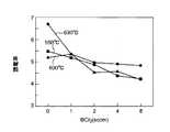
<BCl3 の流量とエッチングレートとの関係>
図7はBCl3 の流量とエッチングレートとの関係を示すグラフである。ここでは図6に示す場合と同じ3種類のエッチング液、すなわち純水[DIW]、希硫酸溶液[SPM]、希フッ酸溶液[DHF]を用いている。従って、各流量について3つのエッチングレートが対応して記載されており、それぞれ左から右に向かってDIWに対するエッチングレート、SPMに対するエッチングレート、DHFに対するエッチングレートの順で記載されている。
また図中の右側には、基準値としてCVDにより形成されたSiN膜(ボロンはノンドープ)のエッチングレートを記載している。尚、図中の左側のBCl3 が”0”sccmの場合は、ALD法により成膜されたSiN膜(ボロンはノンドープ)のエッチングレートを示すことになる。<Relationship between BCl3 flow rate and etching rate>
FIG. 7 is a graph showing the relationship between the flow rate of BCl3 and the etching rate. Here, the same three types of etching solutions as those shown in FIG. 6, namely pure water [DIW], dilute sulfuric acid solution [SPM], and dilute hydrofluoric acid solution [DHF] are used. Accordingly, three etching rates are described correspondingly for each flow rate, and are described in the order of an etching rate for DIW, an etching rate for SPM, and an etching rate for DHF from left to right.
On the right side of the figure, the etching rate of a SiN film (boron is non-doped) formed by CVD is shown as a reference value. When BCl3 on the left side in the drawing is “0” sccm, it indicates the etching rate of the SiN film (boron is non-doped) formed by the ALD method.
また、この場合の各エッチング液に対する許容上限値は、図6において説明した場合と同じであり、DHFは20Å/min、SPMは10Å/min、DIWは5Å/minである。さて、図7から明らかなように、BCl3 の流量を1から8sccmへ増加するに従って、DHF、SPM、DIWに対する各エッチングレートは少しずつ大きくなっており、例えばDHFの場合には5.5Å/minから6.5Å/min程度まで増加し、SPMの場合には0.2Å/minから1.4Å/min程度まで増加し、またDIWの場合には0.1Å/minから0.2Å/min程度まで増加している。しかしながら、各エッチングレートはDHF、SPM、DIWの上記した各許容上限値よりもかなり小さいものであり、従って、全てのSiBN膜は、そのエッチング耐性が十分に高いものであることが確認できた。また参考のためにステップカバレジについても評価したところ、97〜105%の値を示しており、十分に高いことが確認できた。Further, the allowable upper limit value for each etching solution in this case is the same as that described in FIG. 6, DHF is 20 Å / min, SPM is 10 Å / min, and DIW is 5 Å / min. As is apparent from FIG. 7, as the flow rate of BCl3 is increased from 1 to 8 sccm, the etching rates for DHF, SPM, and DIW gradually increase. For example, in the case of DHF, 5.5 Å / In the case of SPM, it increases from about 0.2 Å / min to about 1.4 Å / min, and in the case of DIW, from 0.1 Å / min to 0.2 Å / min. It has increased to the extent. However, each etching rate is considerably smaller than the above-described allowable upper limit values of DHF, SPM, and DIW. Therefore, it was confirmed that all the SiBN films have sufficiently high etching resistance. Moreover, when the step coverage was also evaluated for reference, it showed a value of 97 to 105%, which was confirmed to be sufficiently high.
<第2実施例>
次に本発明方法の第2実施例について説明する。
図8は本発明の成膜方法の第2実施例における各種のガスの供給のタイミングとRF(高周波)の印加のタイミングを示すタイミングチャート、図9は第1及び第2実施例における成膜レートと改善率を示すグラフである。
図3に示した第1実施例においては、DCSガスとBCl3 ガスとを同時に間欠供給する場合において、これらの両ガスの供給休止期間の途中でNH3 ガスを単独で供給するようにしているが、この第2実施例では、NH3 ガスを上記単独供給に加え、DCSガスとBCl3 ガスの同時供給の時もこのNH3 ガスを同時に加えるようにしている。その他の点については、第1実施例の場合と全く同じである。<Second embodiment>
Next, a second embodiment of the method of the present invention will be described.
FIG. 8 is a timing chart showing various gas supply timings and RF (high frequency) application timings in the second embodiment of the film forming method of the present invention, and FIG. 9 is a film forming rate in the first and second embodiments. It is a graph which shows the improvement rate.
In the first embodiment shown in FIG. 3, when DCS gas and BCl3 gas are intermittently supplied simultaneously, NH3 gas is supplied independently during the supply suspension period of these two gases. However, in this second embodiment, NH3 gas is added to the single supply, and this NH3 gas is also added simultaneously when DCS gas and BCl3 gas are supplied simultaneously. The other points are exactly the same as in the first embodiment.
すなわち、ここでは上記シラン系ガスであるDCSガスと上記不純物含有ガスであるBCl3 とを同時に、且つ間欠的に供給し、上記窒化ガスであるNH3 ガスを上記シラン系ガス及び不純物含有ガスと同時に供給すると共に、上記シラン系ガス及び不純物含有ガスの供給停止の期間の途中で上記窒化ガスを単独で供給し、上記窒化ガスを単独で供給する時に上記窒化ガスはプラズマにより活性化される。
上記のように、DCSガス及びBCl3 ガスの両ガスの供給と同時にNH3 ガスも供給することにより、上記DCSガス及びBCl3 ガスのウエハ表面への吸着が促進されるので、ボロン(B)のドーピング量も増加して成膜速度(成膜レート)を上げることができる。That is, here, the DCS gas that is the silane-based gas and the BCl3 that is the impurity-containing gas are supplied simultaneously and intermittently, and the NH3 gas that is the nitriding gas is supplied to the silane-based gas and the impurity-containing gas. At the same time, the nitriding gas is supplied alone during the supply stop period of the silane-based gas and the impurity-containing gas, and the nitriding gas is activated by plasma when the nitriding gas is supplied alone.
As described above, by supplying both the DCS gas and the BCl3 gas simultaneously with the NH3 gas, the adsorption of the DCS gas and the BCl3 gas on the wafer surface is promoted, so that boron (B) Thus, the amount of doping can be increased to increase the deposition rate (deposition rate).
ここで上記DCSガス及びBCl3 ガスの両ガスの供給と同時に供給するNH3 ガスの供給量は、過度に多くしないようにし、例えばDCSガスの供給量以下の量とする。この時のNH3 ガスの供給量が多過ぎると、塩化アンモニウムが多量に発生して排気系の配管が詰まったり、塩化アンモニウムのパーティクルが発生したり、更には、発生する塩化アンモニウムとBCl3 とが簡単に反応することから、Siを含まない、或いはSi成分が非常に少ないBN膜が形成されてしまう。また逆に、NH3 ガスの供給量が少な過ぎると、NH3 ガスを同時供給することの効果が非常に少なくなってしまう。
またNH3 ガスをDCSガス及びBCl3 ガスと同時に供給する際にも、このNH3 ガスをプラズマにより活性化するようにしてもよい(図8(D)中で一点鎖線で示す)。これによれば、DCSガス及びBCl3 ガスのウエハ表面への吸着をより促進させることができるので、その分、成膜レートを更に向上させることができる。Here, the supply amount of the NH3 gas supplied simultaneously with the supply of both the DCS gas and the BCl3 gas is not excessively increased, for example, an amount equal to or less than the supply amount of the DCS gas. If the supply amount of NH3 gas at this time is too large, a large amount of ammonium chloride is generated, the exhaust system piping is clogged, ammonium chloride particles are generated, and the generated ammonium chloride and BCl3 Reacts easily, so that a BN film containing no Si or having a very small Si component is formed. Conversely, if the supply amount of NH3 gas is too small, the effect of simultaneously supplying NH3 gas will be very small.
Further, when the NH3 gas is supplied simultaneously with the DCS gas and the BCl3 gas, the NH3 gas may be activated by plasma (indicated by a one-dot chain line in FIG. 8D). According to this, since adsorption of DCS gas and BCl3 gas to the wafer surface can be further promoted, the film formation rate can be further improved accordingly.
ここで成膜レートについて第1実施例と第2実施例の評価を行ったので、その評価結果について説明する。この評価実験を行った時の各種ガスの流量、プロセス圧力及びプロセス温度等のプロセス条件は先の第1実施例の場合と同じである。そして、第2実施例において、DCSガスとBCl3 ガスの両ガスと同時に供給する時のNH3 ガスの供給量は、DCSガスの供給量の1/10である100sccmに設定している。
図9から明らかなように、ウエハボート中のウエハ載置位置を示すTOP(上段)、CTR(中段)及びBTM(下段)の各位置において、成膜レートは第1実施例よりも第2実施例の方が全て高くなっており、成膜レート(Å/サイクル)が改善されていることが確認できた。具体的な成膜レートの改善率(増加率)は、TOPの位置で161%、CTRの位置で161%、BTMの位置で152%であり、全てのウエハ載置位置において成膜レートを大幅に増加して高い改善率を得られることが確認できた。Here, since the evaluation of the first embodiment and the second embodiment was performed with respect to the film formation rate, the evaluation results will be described. Process conditions such as flow rates of various gases, process pressure, and process temperature when this evaluation experiment is performed are the same as those in the first embodiment. In the second embodiment, the supply amount of NH3 gas when the DCS gas and the BCl3 gas are supplied simultaneously is set to 100 sccm, which is 1/10 of the supply amount of the DCS gas.
As is apparent from FIG. 9, the film formation rate in the TOP (upper stage), CTR (middle stage), and BTM (lower stage) positions indicating the wafer placement position in the wafer boat is set to be higher than that in the first embodiment. All of the examples were higher, and it was confirmed that the film formation rate (Å / cycle) was improved. Specific improvement rate (increase rate) of the film formation rate is 161% at the TOP position, 161% at the CTR position, and 152% at the BTM position. The film formation rate is greatly increased at all wafer placement positions. It was confirmed that a high improvement rate can be obtained.
上記各実施例では、不純物含有シリコン窒化膜に関して主として誘電率やエッチングレートに着目して説明したが、この他に素子の高速動作に大きな影響を与える電子の移動度(モビリティ)についても考察する必要がある。
上記した電子の移動度を高めるためには、不純物含有シリコン窒化膜にストレスを与えるのが好ましいが、この場合、ストレスには引っ張り的なストレス(テンサイルストレス)と圧縮的なストレス(コンプレッシブストレス)とがある。In each of the above embodiments, the impurity-containing silicon nitride film has been described mainly focusing on the dielectric constant and the etching rate, but in addition to this, it is necessary to consider the mobility of electrons (mobility) that has a large influence on the high-speed operation of the device. There is.
In order to increase the electron mobility described above, it is preferable to apply stress to the impurity-containing silicon nitride film. In this case, the stress includes tensile stress (tensile stress) and compressive stress (compressive stress). )
ここで図10はNMOSとPMOSのトランジスタの概略構成図を示し、図中、矢印は圧力の方向を表している。図10(A)に示すように、例えばNMOS素子の場合には、トランジスタのチャネルにコンプレッシブストレスが印加されるのが好ましい。この場合、トランジスタのカバー膜は高テンサイルストレスの膜により作られる。また、図10(B)に示すように、PMOS素子の場合には、トランジスタのチャネルにテンサイルストレスが印加されるのが好ましい。この場合、トランジスタのカバー膜は高コンプレッシブストレスの膜により作られる。しかし、従来はコンプレッシブストレスの不純物含有シリコン窒化膜を形成するのが困難であり、またストレス自体の大きさも制御するのが困難であった。 Here, FIG. 10 shows a schematic configuration diagram of an NMOS transistor and a PMOS transistor. In the drawing, an arrow indicates a direction of pressure. As shown in FIG. 10A, for example, in the case of an NMOS element, it is preferable that a compressive stress is applied to the channel of the transistor. In this case, the cover film of the transistor is made of a high tensile stress film. As shown in FIG. 10B, in the case of a PMOS device, it is preferable that a tensile stress is applied to the channel of the transistor. In this case, the cover film of the transistor is made of a highly compressive stress film. However, conventionally, it has been difficult to form an impurity-containing silicon nitride film having a compressive stress, and it has been difficult to control the magnitude of the stress itself.
しかしながら、本発明者等の研究により、成膜時に供給する不純物含有ガスの供給量を制御することにより、上記不純物含有シリコン窒化膜のストレスの大きさ及びストレスの種類を制御できることが判明した。
すなわち、上記第1及び第2実施例において、前記不純物含有ガスの供給量を制御することにより、前記被処理体上に形成される前記不純物含有シリコン窒化膜に所望のストレスを付与することができる。
この場合、不純物含有ガスの供給量を、特定の領域に適宜変化させることによって、不純物含有シリコン窒化膜に付与するストレスの種類を、コンプレッシブストレスとテンサイルストレスとのいずれかに設定することができる。However, the inventors' research has revealed that the magnitude and type of stress of the impurity-containing silicon nitride film can be controlled by controlling the supply amount of the impurity-containing gas supplied during film formation.
That is, in the first and second embodiments, a desired stress can be applied to the impurity-containing silicon nitride film formed on the target object by controlling the supply amount of the impurity-containing gas. .
In this case, the type of stress applied to the impurity-containing silicon nitride film can be set to either compressive stress or tensile stress by appropriately changing the supply amount of the impurity-containing gas to a specific region. it can.
ここで、実際に不純物含有ガスであるBCl3 の流量を種々変更した時に形成された不純物含有シリコン窒化膜のストレスの変化を測定したので、その測定結果について図11を参照して説明する。
図11(A)はプロセス温度が550℃の場合を示し、図11(B)はプロセス温度が630℃の場合を示す。また図11において、縦軸の”+”側はテンサイルストレスを示し、”−”側はコンプレッシブストレスを示す。この時のDCSガスの流量は1000sccm、NH3 ガスの流量は1000sccmである。Here, since the change in stress of the impurity-containing silicon nitride film formed when the flow rate of BCl3 as the impurity-containing gas is actually changed is measured, the measurement result will be described with reference to FIG.
FIG. 11A shows the case where the process temperature is 550 ° C., and FIG. 11B shows the case where the process temperature is 630 ° C. In FIG. 11, the “+” side of the vertical axis represents the tensile stress, and the “−” side represents the compressive stress. At this time, the flow rate of DCS gas is 1000 sccm, and the flow rate of NH3 gas is 1000 sccm.
まず、図11(A)に示す場合、BCl3 ガスの流量を、0、8、15sccmにそれぞれ設定した時のストレスを示す。この図11(A)から明らかなように、BCl3 ガスの流量が”0”の時は(不純物のドープなし)、ストレスが1143MPaとなって非常に高い。これに対して、BCl3 ガスの流量を8、15sccmという具合に増加すると、ストレス(テンサイル)は135、111MPaという具合に順次低下している。従って、BCl3 ガスの流量を適宜選択することにより、所望する大きさのストレス(テンサイル)を不純物含有シリコン窒化膜に付与できることが判明する。First, in the case shown in FIG. 11A, the stress when the flow rate of the BCl3 gas is set to 0, 8, and 15 sccm, respectively, is shown. As is apparent from FIG. 11A, when the flow rate of the BCl3 gas is “0” (no impurity doping), the stress is 1143 MPa, which is very high. On the other hand, when the flow rate of the BCl3 gas is increased to 8, 15 sccm, the stress (tensile) gradually decreases to 135, 111 MPa. Therefore, it is found that a desired amount of stress (tensile) can be applied to the impurity-containing silicon nitride film by appropriately selecting the flow rate of the BCl3 gas.
また図11(B)に示す場合は、BCl3 ガスの流量を、1、2、4、8sccmにそれぞれ設定した時のストレスを示す。この図11(B)から明らかなように、BCl3 ガスの流量を増加して行くと、ストレスが220、113、76MPaという具合に順次減少し、そして、8sccmの時には、ストレスは−78MPaとなって、ストレスの種類はテンサイルからコンプレッシブへと転換していることが判明する。このように、プロセス温度630℃の時には、BCl3 ガスの流量により、ストレスの大きさのみならず、ストレスの種類(方向)も制御できることが判明する。
尚、上述したプロセス温度及びガス流量は、それぞれ単に一例を示したに過ぎず、必要に応じてそれぞれ種々変更して最適なストレスの大きさ及びストレスの種類(方向)を選択することができる。11B shows stress when the flow rate of the BCl3 gas is set to 1, 2, 4, 8 sccm, respectively. As is apparent from FIG. 11B, when the flow rate of the BCl3 gas is increased, the stress is sequentially reduced to 220, 113, 76 MPa, and the stress becomes −78 MPa at 8 sccm. Thus, it turns out that the type of stress has changed from the tensil to the compressive. Thus, when the process temperature is 630 ° C., it is found that not only the magnitude of stress but also the type (direction) of stress can be controlled by the flow rate of BCl3 gas.
Note that the above-described process temperature and gas flow rate are merely examples, and various changes can be made as necessary to select the optimum stress magnitude and stress type (direction).
また上記各実施例では、シラン系ガスとしてDCSガスを用いたが、これに限定されず、ジクロロシラン(DCS)、ヘキサクロロジシラン(HCD)、モノシラン[SiH4 ]、ジシラン[Si2 H6 ]、ヘキサメチルジシラザン(HMDS)、テトラクロロシラン(TCS)、ジシリルアミン(DSA)、トリシリルアミン(TSA)、ビスターシャルブチルアミノシラン(BTBAS)よりなる群より選択される1以上のガスを用いることができる。
また、上記各実施例では、窒化ガスとしてNH3 ガスを用いたが、これに限定されず、アンモニア[NH3 ]、窒素[N2 ]、一酸化二窒素[N2 O]、一酸化窒素[NO]よりなる群より選択される1以上のガスを用いることができる。
また、上記各実施例では、不純物含有ガスとしてBCl3 ガスを用いたが、これに限定されず、BCl3 、B2 H6 、BF3 、B(CH3 )3 よりなる群より選択される1以上のガスを用いることができる。In each of the above embodiments, DCS gas is used as the silane-based gas. However, the present invention is not limited to this, and dichlorosilane (DCS), hexachlorodisilane (HCD), monosilane [SiH4 ], disilane [Si2 H6 ], One or more gases selected from the group consisting of hexamethyldisilazane (HMDS), tetrachlorosilane (TCS), disilylamine (DSA), trisilylamine (TSA), and binary butylaminosilane (BTBAS) can be used.
In each of the above embodiments, NH3 gas is used as the nitriding gas. However, the present invention is not limited to this. Ammonia [NH3 ], nitrogen [N2 ], dinitrogen monoxide [N2 O], and nitric oxide One or more gases selected from the group consisting of [NO] can be used.
In each of the above embodiments, BCl3 gas is used as the impurity-containing gas. However, the gas is not limited to this, and is selected from the group consisting of BCl3 , B2 H6 , BF3 , and B (CH3 )3. One or more gases can be used.
また更に、ここでは成膜装置2として、プラズマを形成する活性化手段50を処理容器4に一体的に組み込んだ装置例について説明したが、これに限定されず、この活性化手段50を処理容器4とは別体で設け、NH3 ガスを処理容器4の外で予め活性化(いわゆるリモートプラズマ)、その活性化NH3 ガスを処理容器4内へ供給するようにしてもよい。
また被処理体としては、半導体ウエハに限定されず、ガラス基板、LCD基板、セラミック基板等にも本発明を適用することができる。Furthermore, although the example of the apparatus in which the activation means 50 for forming plasma is integrally incorporated in the
The object to be processed is not limited to a semiconductor wafer, and the present invention can be applied to a glass substrate, an LCD substrate, a ceramic substrate, and the like.
2 成膜装置
4 処理容器
12 ウエハボート(供給手段)
28 窒化ガス供給手段
30 シラン系ガス供給手段
31 不純物含有ガス供給手段
32 パージガス供給手段
34 窒化ガス分散ノズル
36 シラン系ガス分散ノズル
37 不純物含有ガス分散ノズル
48 制御手段
50 活性化手段
58 プラズマ電極
60 高周波電源
70 加熱手段
W 半導体ウエハ(被処理体)
2
28 Nitriding gas supply means 30 Silane-based gas supply means 31 Impurity-containing gas supply means 32 Purge gas supply means 34 Nitriding
Claims (20)
Translated fromJapanese前記シラン系ガスと前記窒化ガスとを交互に供給すると共に、前記不純物含有ガスを前記シラン系ガスと同時に供給し、前記窒化ガスはプラズマにより活性化されることを特徴とする成膜方法。A processing vessel made evacuatedis composed of a silane-based gas, a nitriding gas, andone or more boron-containing gases selected from the group consisting ofBCl3, B2H6, BF3, and B (CH3)3. In a film forming method for forming a thin film made of an impurity-containing silicon nitride film on the surface of an object to be processed by supplying an impurity-containing gas,
A film forming method, wherein the silane-based gas and the nitriding gas are alternately supplied, the impurity-containing gas is supplied simultaneously with the silane-based gas, and the nitriding gas is activated by plasma.
前記シラン系ガスと前記不純物含有ガスとを同時に、且つ間欠的に供給し、前記窒化ガスを前記シラン系ガス及び不純物含有ガスと同時に供給すると共に、前記シラン系ガス及び不純物含有ガスの供給停止の期間の途中で前記窒化ガスを単独で供給し、前記窒化ガスを単独で供給する時に前記窒化ガスはプラズマにより活性化されることを特徴とする成膜方法。A processing vessel made evacuatedis composed of a silane-based gas, a nitriding gas, andone or more boron-containing gases selected from the group consisting ofBCl3, B2H6, BF3, and B (CH3)3. In a film forming method for forming a thin film made of an impurity-containing silicon nitride film on the surface of an object to be processed by supplying an impurity-containing gas,
The silane-based gas and the impurity-containing gas are supplied simultaneously and intermittently, the nitriding gas is supplied simultaneously with the silane-based gas and the impurity-containing gas, and the supply of the silane-based gas and the impurity-containing gas is stopped. A film forming method, wherein the nitriding gas is supplied alone during the period, and the nitriding gas is activated by plasma when the nitriding gas is supplied alone.
真空引き可能になされた縦型の筒体状の処理容器と、
前記被処理体を複数段に保持して前記処理容器内に挿脱される保持手段と、
前記処理容器の外周に設けられる加熱手段と、
前記処理容器内へ成膜用のシラン系ガスを供給するシラン系ガス供給手段と、
前記処理容器内へ窒化ガスを供給する窒化ガス供給手段と、
前記処理容器内へBCl3 、B2 H6 、BF3 、B(CH3 )3 よりなる群より選択される1以上のボロン含有ガスよりなる不純物含有ガスを供給する不純物含有ガス供給手段と、
前記窒化ガスを活性化する活性化手段と、
請求項1乃至16のいずれか一項に記載の成膜方法を実施するように装置全体を制御する制御手段と、
を備えたことを特徴とする成膜装置。In a film forming apparatus for forming a predetermined thin film on an object to be processed,
A vertical cylindrical processing container made evacuated,
Holding means for holding the object to be processed in a plurality of stages and being inserted into and removed from the processing container;
Heating means provided on the outer periphery of the processing container;
Silane-based gas supply means for supplying a silane-based gas for film formation into the processing container;
Nitriding gas supply means for supplying a nitriding gas into the processing vessel;
Impurity-containing gas supply means for supplying an impurity-containing gas made ofone or more boron-containing gases selected from the group consisting ofBCl3, B2H6, BF3, B (CH3)3into the processing container;
Activating means for activating the nitriding gas;
Control meansfor controlling theentire apparatus so as to carry out the film forming method according to claim 1 ;
A film forming apparatus comprising:
被処理体を複数段に保持して前記処理容器内に挿脱される保持手段と、
前記処理容器の外周に設けられる加熱手段と、
前記処理容器内へ成膜用のシラン系ガスを供給するシラン系ガス供給手段と、
前記処理容器内へ窒化ガスを供給する窒化ガス供給手段と、
前記処理容器内へBCl3 、B2 H6 、BF3 、B(CH3 )3 よりなる群より選択される1以上のボロン含有ガスよりなる不純物含有ガスを供給する不純物含有ガス供給手段と、
前記窒化ガスを活性化する活性化手段と、
装置全体を制御する制御手段とを有する成膜装置を用いて薄膜を形成するに際して、
請求項1乃至16のいずれか一項に記載の成膜方法を実施するように前記成膜装置を制御するプログラムを記憶する記憶媒体。A vertical cylindrical processing container made evacuated,
Holding means for holding the object to be processed in a plurality of stages and being inserted into and removed from the processing container;
Heating means provided on the outer periphery of the processing container;
Silane-based gas supply means for supplying a silane-based gas for film formation into the processing container;
Nitriding gas supply means for supplying a nitriding gas into the processing vessel;
Impurity-containing gas supply means for supplying an impurity-containing gas made of one or more boron-containing gases selected from the group consisting ofBCl3, B2H6, BF3, B (CH3)3into the processing container;
Activating means for activating the nitriding gas;
When forming a thin film using a film forming apparatushaving a control means for controlling the entire apparatus ,
A storage medium for storing a program for controlling the film forming apparatusso as to perform the film forming method according to claim 1 .
Priority Applications (5)
| Application Number | Priority Date | Filing Date | Title |
|---|---|---|---|
| JP2005177344AJP4179311B2 (en) | 2004-07-28 | 2005-06-17 | Film forming method, film forming apparatus, and storage medium |
| US11/188,736US7462571B2 (en) | 2004-07-28 | 2005-07-26 | Film formation method and apparatus for semiconductor process for forming a silicon nitride film |
| TW094125436ATWI349302B (en) | 2004-07-28 | 2005-07-27 | Film formation method and apparatus for semiconductor process |
| KR1020050068174AKR100890684B1 (en) | 2004-07-28 | 2005-07-27 | Film formation method for semiconductor process |
| CNB2005100873066ACN100426474C (en) | 2004-07-28 | 2005-07-28 | Film formation method and device for semiconductor process |
Applications Claiming Priority (3)
| Application Number | Priority Date | Filing Date | Title |
|---|---|---|---|
| JP2004220555 | 2004-07-28 | ||
| JP2005048060 | 2005-02-23 | ||
| JP2005177344AJP4179311B2 (en) | 2004-07-28 | 2005-06-17 | Film forming method, film forming apparatus, and storage medium |
Publications (3)
| Publication Number | Publication Date |
|---|---|
| JP2006270016A JP2006270016A (en) | 2006-10-05 |
| JP2006270016A5 JP2006270016A5 (en) | 2006-12-28 |
| JP4179311B2true JP4179311B2 (en) | 2008-11-12 |
Family
ID=35798796
Family Applications (1)
| Application Number | Title | Priority Date | Filing Date |
|---|---|---|---|
| JP2005177344AExpired - LifetimeJP4179311B2 (en) | 2004-07-28 | 2005-06-17 | Film forming method, film forming apparatus, and storage medium |
Country Status (5)
| Country | Link |
|---|---|
| US (1) | US7462571B2 (en) |
| JP (1) | JP4179311B2 (en) |
| KR (1) | KR100890684B1 (en) |
| CN (1) | CN100426474C (en) |
| TW (1) | TWI349302B (en) |
Families Citing this family (368)
| Publication number | Priority date | Publication date | Assignee | Title |
|---|---|---|---|---|
| JP4279176B2 (en)* | 2004-03-02 | 2009-06-17 | 株式会社アルバック | Method for forming silicon nitride film |
| JP4396547B2 (en)* | 2004-06-28 | 2010-01-13 | 東京エレクトロン株式会社 | Film forming method, film forming apparatus, and storage medium |
| JP4997698B2 (en)* | 2004-12-09 | 2012-08-08 | 富士通セミコンダクター株式会社 | Stress storage insulating film manufacturing method and semiconductor device |
| JP4258518B2 (en)* | 2005-03-09 | 2009-04-30 | 東京エレクトロン株式会社 | Film forming method, film forming apparatus, and storage medium |
| US8138104B2 (en)* | 2005-05-26 | 2012-03-20 | Applied Materials, Inc. | Method to increase silicon nitride tensile stress using nitrogen plasma in-situ treatment and ex-situ UV cure |
| US8129290B2 (en)* | 2005-05-26 | 2012-03-06 | Applied Materials, Inc. | Method to increase tensile stress of silicon nitride films using a post PECVD deposition UV cure |
| WO2007008653A2 (en)* | 2005-07-08 | 2007-01-18 | Aviza Technology, Inc. | Method for depositing silicon-containing films |
| KR101047230B1 (en)* | 2006-03-28 | 2011-07-06 | 가부시키가이샤 히다치 고쿠사이 덴키 | Substrate treating apparatus |
| JP4929932B2 (en)* | 2006-09-01 | 2012-05-09 | 東京エレクトロン株式会社 | Film forming method, film forming apparatus, and storage medium |
| JP4916257B2 (en)* | 2006-09-06 | 2012-04-11 | 東京エレクトロン株式会社 | Oxide film forming method, oxide film forming apparatus and program |
| US20080145536A1 (en)* | 2006-12-13 | 2008-06-19 | Applied Materials, Inc. | METHOD AND APPARATUS FOR LOW TEMPERATURE AND LOW K SiBN DEPOSITION |
| KR100843231B1 (en)* | 2007-01-23 | 2008-07-02 | 삼성전자주식회사 | Plasma Doping Method |
| US20080213479A1 (en)* | 2007-02-16 | 2008-09-04 | Tokyo Electron Limited | SiCN film formation method and apparatus |
| JP4924437B2 (en)* | 2007-02-16 | 2012-04-25 | 東京エレクトロン株式会社 | Film forming method and film forming apparatus |
| JP2008294260A (en)* | 2007-05-25 | 2008-12-04 | Sony Corp | Semiconductor device and manufacturing method therefor, and laminate insulating film and forming method therefor |
| JP5151260B2 (en)* | 2007-06-11 | 2013-02-27 | 東京エレクトロン株式会社 | Film forming method and film forming apparatus |
| US20090056877A1 (en) | 2007-08-31 | 2009-03-05 | Tokyo Electron Limited | Plasma processing apparatus |
| JP4935684B2 (en)* | 2008-01-12 | 2012-05-23 | 東京エレクトロン株式会社 | Film forming method and film forming apparatus |
| US20090197424A1 (en)* | 2008-01-31 | 2009-08-06 | Hitachi Kokusai Electric Inc. | Substrate processing apparatus and method for manufacturing semiconductor device |
| JP2009260151A (en)* | 2008-04-18 | 2009-11-05 | Tokyo Electron Ltd | Method of forming metal doped layer, film forming apparatus, and storage medium |
| JP5284182B2 (en)* | 2008-07-23 | 2013-09-11 | 株式会社日立国際電気 | Substrate processing apparatus and semiconductor device manufacturing method |
| JP5155070B2 (en) | 2008-09-02 | 2013-02-27 | 株式会社日立国際電気 | Semiconductor device manufacturing method, substrate processing method, and substrate processing apparatus |
| JP4638550B2 (en) | 2008-09-29 | 2011-02-23 | 東京エレクトロン株式会社 | Mask pattern forming method, fine pattern forming method, and film forming apparatus |
| JP5384291B2 (en) | 2008-11-26 | 2014-01-08 | 株式会社日立国際電気 | Semiconductor device manufacturing method, substrate processing method, and substrate processing apparatus |
| JP5099101B2 (en) | 2009-01-23 | 2012-12-12 | 東京エレクトロン株式会社 | Plasma processing equipment |
| JP5136574B2 (en) | 2009-05-01 | 2013-02-06 | 東京エレクトロン株式会社 | Plasma processing apparatus and plasma processing method |
| GB2471128A (en)* | 2009-06-18 | 2010-12-22 | Rec Solar As | Surface passivation of silicon wafers |
| JP2011023576A (en)* | 2009-07-16 | 2011-02-03 | Hitachi Kokusai Electric Inc | Method of manufacturing semiconductor device, and device for treating substrate |
| US8956983B2 (en) | 2010-04-15 | 2015-02-17 | Novellus Systems, Inc. | Conformal doping via plasma activated atomic layer deposition and conformal film deposition |
| US9076646B2 (en) | 2010-04-15 | 2015-07-07 | Lam Research Corporation | Plasma enhanced atomic layer deposition with pulsed plasma exposure |
| US9257274B2 (en) | 2010-04-15 | 2016-02-09 | Lam Research Corporation | Gapfill of variable aspect ratio features with a composite PEALD and PECVD method |
| US9373500B2 (en) | 2014-02-21 | 2016-06-21 | Lam Research Corporation | Plasma assisted atomic layer deposition titanium oxide for conformal encapsulation and gapfill applications |
| US9611544B2 (en) | 2010-04-15 | 2017-04-04 | Novellus Systems, Inc. | Plasma activated conformal dielectric film deposition |
| US8637411B2 (en) | 2010-04-15 | 2014-01-28 | Novellus Systems, Inc. | Plasma activated conformal dielectric film deposition |
| US9390909B2 (en) | 2013-11-07 | 2016-07-12 | Novellus Systems, Inc. | Soft landing nanolaminates for advanced patterning |
| US20110256734A1 (en) | 2010-04-15 | 2011-10-20 | Hausmann Dennis M | Silicon nitride films and methods |
| US9997357B2 (en) | 2010-04-15 | 2018-06-12 | Lam Research Corporation | Capped ALD films for doping fin-shaped channel regions of 3-D IC transistors |
| US9892917B2 (en) | 2010-04-15 | 2018-02-13 | Lam Research Corporation | Plasma assisted atomic layer deposition of multi-layer films for patterning applications |
| JP5696530B2 (en)* | 2010-05-01 | 2015-04-08 | 東京エレクトロン株式会社 | Thin film forming method and film forming apparatus |
| US9685320B2 (en) | 2010-09-23 | 2017-06-20 | Lam Research Corporation | Methods for depositing silicon oxide |
| JP5665627B2 (en)* | 2011-03-30 | 2015-02-04 | 東京エレクトロン株式会社 | Method for stacking silicon oxide film and silicon nitride film, film forming apparatus, and method for manufacturing semiconductor device |
| US8647993B2 (en) | 2011-04-11 | 2014-02-11 | Novellus Systems, Inc. | Methods for UV-assisted conformal film deposition |
| US20130023129A1 (en) | 2011-07-20 | 2013-01-24 | Asm America, Inc. | Pressure transmitter for a semiconductor processing environment |
| JP5723243B2 (en) | 2011-08-11 | 2015-05-27 | 東京エレクトロン株式会社 | Film forming method, semiconductor device manufacturing method including the same, film forming apparatus, and semiconductor device |
| KR101879175B1 (en)* | 2011-10-20 | 2018-08-20 | 삼성전자주식회사 | Chemical Vapor Deposition Apparatus |
| US8592328B2 (en) | 2012-01-20 | 2013-11-26 | Novellus Systems, Inc. | Method for depositing a chlorine-free conformal sin film |
| US9388491B2 (en)* | 2012-07-23 | 2016-07-12 | Novellus Systems, Inc. | Method for deposition of conformal films with catalysis assisted low temperature CVD |
| US10714315B2 (en) | 2012-10-12 | 2020-07-14 | Asm Ip Holdings B.V. | Semiconductor reaction chamber showerhead |
| KR102207992B1 (en) | 2012-10-23 | 2021-01-26 | 램 리써치 코포레이션 | Sub-saturated atomic layer deposition and conformal film deposition |
| SG2013083241A (en) | 2012-11-08 | 2014-06-27 | Novellus Systems Inc | Conformal film deposition for gapfill |
| JP6538300B2 (en) | 2012-11-08 | 2019-07-03 | ノベラス・システムズ・インコーポレーテッドNovellus Systems Incorporated | Method for depositing a film on a sensitive substrate |
| JP5956972B2 (en)* | 2012-12-21 | 2016-07-27 | 東京エレクトロン株式会社 | Deposition method |
| US20160376700A1 (en) | 2013-02-01 | 2016-12-29 | Asm Ip Holding B.V. | System for treatment of deposition reactor |
| TWI502096B (en) | 2013-06-17 | 2015-10-01 | Ind Tech Res Inst | Reaction device and manufacture method for chemical vapor deposition |
| JP6267080B2 (en) | 2013-10-07 | 2018-01-24 | 東京エレクトロン株式会社 | Method and apparatus for forming silicon nitride film |
| US9556516B2 (en)* | 2013-10-09 | 2017-01-31 | ASM IP Holding B.V | Method for forming Ti-containing film by PEALD using TDMAT or TDEAT |
| US20150125628A1 (en)* | 2013-11-06 | 2015-05-07 | Asm Ip Holding B.V. | Method of depositing thin film |
| US9214334B2 (en) | 2014-02-18 | 2015-12-15 | Lam Research Corporation | High growth rate process for conformal aluminum nitride |
| JP6291297B2 (en) | 2014-03-17 | 2018-03-14 | 東京エレクトロン株式会社 | Film forming method, film forming apparatus, and storage medium |
| US11015245B2 (en) | 2014-03-19 | 2021-05-25 | Asm Ip Holding B.V. | Gas-phase reactor and system having exhaust plenum and components thereof |
| JP6307984B2 (en)* | 2014-03-31 | 2018-04-11 | 東京エレクトロン株式会社 | Substrate processing equipment |
| JP6504770B2 (en) | 2014-06-30 | 2019-04-24 | 東京エレクトロン株式会社 | PLASMA PROCESSING APPARATUS AND PLASMA PROCESSING METHOD |
| US9478438B2 (en) | 2014-08-20 | 2016-10-25 | Lam Research Corporation | Method and apparatus to deposit pure titanium thin film at low temperature using titanium tetraiodide precursor |
| US9478411B2 (en) | 2014-08-20 | 2016-10-25 | Lam Research Corporation | Method to tune TiOx stoichiometry using atomic layer deposited Ti film to minimize contact resistance for TiOx/Ti based MIS contact scheme for CMOS |
| US9214333B1 (en) | 2014-09-24 | 2015-12-15 | Lam Research Corporation | Methods and apparatuses for uniform reduction of the in-feature wet etch rate of a silicon nitride film formed by ALD |
| US10941490B2 (en) | 2014-10-07 | 2021-03-09 | Asm Ip Holding B.V. | Multiple temperature range susceptor, assembly, reactor and system including the susceptor, and methods of using the same |
| US9564312B2 (en)* | 2014-11-24 | 2017-02-07 | Lam Research Corporation | Selective inhibition in atomic layer deposition of silicon-containing films |
| US9589790B2 (en) | 2014-11-24 | 2017-03-07 | Lam Research Corporation | Method of depositing ammonia free and chlorine free conformal silicon nitride film |
| JP6378070B2 (en)* | 2014-12-15 | 2018-08-22 | 東京エレクトロン株式会社 | Deposition method |
| US10276355B2 (en) | 2015-03-12 | 2019-04-30 | Asm Ip Holding B.V. | Multi-zone reactor, system including the reactor, and method of using the same |
| US10566187B2 (en) | 2015-03-20 | 2020-02-18 | Lam Research Corporation | Ultrathin atomic layer deposition film accuracy thickness control |
| US9502238B2 (en) | 2015-04-03 | 2016-11-22 | Lam Research Corporation | Deposition of conformal films by atomic layer deposition and atomic layer etch |
| TWI663281B (en)* | 2015-06-16 | 2019-06-21 | 美商慧盛材料美國責任有限公司 | Preparation and composition of halidosilane compounds, and container containing same |
| US10458018B2 (en) | 2015-06-26 | 2019-10-29 | Asm Ip Holding B.V. | Structures including metal carbide material, devices including the structures, and methods of forming same |
| US10526701B2 (en) | 2015-07-09 | 2020-01-07 | Lam Research Corporation | Multi-cycle ALD process for film uniformity and thickness profile modulation |
| US9601693B1 (en) | 2015-09-24 | 2017-03-21 | Lam Research Corporation | Method for encapsulating a chalcogenide material |
| US10211308B2 (en) | 2015-10-21 | 2019-02-19 | Asm Ip Holding B.V. | NbMC layers |
| US10121655B2 (en) | 2015-11-20 | 2018-11-06 | Applied Materials, Inc. | Lateral plasma/radical source |
| US11139308B2 (en) | 2015-12-29 | 2021-10-05 | Asm Ip Holding B.V. | Atomic layer deposition of III-V compounds to form V-NAND devices |
| US10529554B2 (en) | 2016-02-19 | 2020-01-07 | Asm Ip Holding B.V. | Method for forming silicon nitride film selectively on sidewalls or flat surfaces of trenches |
| WO2017149604A1 (en)* | 2016-02-29 | 2017-09-08 | 株式会社日立国際電気 | Method for manufacturing semiconductor device, substrate processing apparatus, and recording medium |
| US10343920B2 (en) | 2016-03-18 | 2019-07-09 | Asm Ip Holding B.V. | Aligned carbon nanotubes |
| JP6529927B2 (en)* | 2016-04-15 | 2019-06-12 | 株式会社Kokusai Electric | Semiconductor device manufacturing method, substrate processing apparatus, and program |
| US10367080B2 (en) | 2016-05-02 | 2019-07-30 | Asm Ip Holding B.V. | Method of forming a germanium oxynitride film |
| US11453943B2 (en) | 2016-05-25 | 2022-09-27 | Asm Ip Holding B.V. | Method for forming carbon-containing silicon/metal oxide or nitride film by ALD using silicon precursor and hydrocarbon precursor |
| US9773643B1 (en) | 2016-06-30 | 2017-09-26 | Lam Research Corporation | Apparatus and method for deposition and etch in gap fill |
| US10062563B2 (en) | 2016-07-01 | 2018-08-28 | Lam Research Corporation | Selective atomic layer deposition with post-dose treatment |
| US9859151B1 (en) | 2016-07-08 | 2018-01-02 | Asm Ip Holding B.V. | Selective film deposition method to form air gaps |
| US10612137B2 (en) | 2016-07-08 | 2020-04-07 | Asm Ip Holdings B.V. | Organic reactants for atomic layer deposition |
| KR102532607B1 (en) | 2016-07-28 | 2023-05-15 | 에이에스엠 아이피 홀딩 비.브이. | Substrate processing apparatus and method of operating the same |
| US9812320B1 (en) | 2016-07-28 | 2017-11-07 | Asm Ip Holding B.V. | Method and apparatus for filling a gap |
| US9887082B1 (en) | 2016-07-28 | 2018-02-06 | Asm Ip Holding B.V. | Method and apparatus for filling a gap |
| US10629435B2 (en) | 2016-07-29 | 2020-04-21 | Lam Research Corporation | Doped ALD films for semiconductor patterning applications |
| KR102146600B1 (en)* | 2016-08-01 | 2020-08-20 | 도쿄엘렉트론가부시키가이샤 | Substrate processing apparatus and substrate processing method |
| US10037884B2 (en) | 2016-08-31 | 2018-07-31 | Lam Research Corporation | Selective atomic layer deposition for gapfill using sacrificial underlayer |
| US10074543B2 (en) | 2016-08-31 | 2018-09-11 | Lam Research Corporation | High dry etch rate materials for semiconductor patterning applications |
| US9865455B1 (en) | 2016-09-07 | 2018-01-09 | Lam Research Corporation | Nitride film formed by plasma-enhanced and thermal atomic layer deposition process |
| KR102698026B1 (en)* | 2016-09-28 | 2024-08-21 | 삼성전자주식회사 | Method for forming dielectric layer and Method for fabricating semiconductor device |
| US11532757B2 (en) | 2016-10-27 | 2022-12-20 | Asm Ip Holding B.V. | Deposition of charge trapping layers |
| US10714350B2 (en) | 2016-11-01 | 2020-07-14 | ASM IP Holdings, B.V. | Methods for forming a transition metal niobium nitride film on a substrate by atomic layer deposition and related semiconductor device structures |
| US10832908B2 (en) | 2016-11-11 | 2020-11-10 | Lam Research Corporation | Self-aligned multi-patterning process flow with ALD gapfill spacer mask |
| US10454029B2 (en) | 2016-11-11 | 2019-10-22 | Lam Research Corporation | Method for reducing the wet etch rate of a sin film without damaging the underlying substrate |
| US10134579B2 (en) | 2016-11-14 | 2018-11-20 | Lam Research Corporation | Method for high modulus ALD SiO2 spacer |
| KR102546317B1 (en) | 2016-11-15 | 2023-06-21 | 에이에스엠 아이피 홀딩 비.브이. | Gas supply unit and substrate processing apparatus including the same |
| KR102762543B1 (en) | 2016-12-14 | 2025-02-05 | 에이에스엠 아이피 홀딩 비.브이. | Substrate processing apparatus |
| US11581186B2 (en) | 2016-12-15 | 2023-02-14 | Asm Ip Holding B.V. | Sequential infiltration synthesis apparatus |
| US11447861B2 (en) | 2016-12-15 | 2022-09-20 | Asm Ip Holding B.V. | Sequential infiltration synthesis apparatus and a method of forming a patterned structure |
| KR102700194B1 (en) | 2016-12-19 | 2024-08-28 | 에이에스엠 아이피 홀딩 비.브이. | Substrate processing apparatus |
| US10269558B2 (en) | 2016-12-22 | 2019-04-23 | Asm Ip Holding B.V. | Method of forming a structure on a substrate |
| US11390950B2 (en) | 2017-01-10 | 2022-07-19 | Asm Ip Holding B.V. | Reactor system and method to reduce residue buildup during a film deposition process |
| US10468261B2 (en) | 2017-02-15 | 2019-11-05 | Asm Ip Holding B.V. | Methods for forming a metallic film on a substrate by cyclical deposition and related semiconductor device structures |
| US10529563B2 (en) | 2017-03-29 | 2020-01-07 | Asm Ip Holdings B.V. | Method for forming doped metal oxide films on a substrate by cyclical deposition and related semiconductor device structures |
| US10770286B2 (en) | 2017-05-08 | 2020-09-08 | Asm Ip Holdings B.V. | Methods for selectively forming a silicon nitride film on a substrate and related semiconductor device structures |
| US12040200B2 (en) | 2017-06-20 | 2024-07-16 | Asm Ip Holding B.V. | Semiconductor processing apparatus and methods for calibrating a semiconductor processing apparatus |
| US11306395B2 (en) | 2017-06-28 | 2022-04-19 | Asm Ip Holding B.V. | Methods for depositing a transition metal nitride film on a substrate by atomic layer deposition and related deposition apparatus |
| KR20190009245A (en) | 2017-07-18 | 2019-01-28 | 에이에스엠 아이피 홀딩 비.브이. | Methods for forming a semiconductor device structure and related semiconductor device structures |
| US11018002B2 (en) | 2017-07-19 | 2021-05-25 | Asm Ip Holding B.V. | Method for selectively depositing a Group IV semiconductor and related semiconductor device structures |
| US10541333B2 (en) | 2017-07-19 | 2020-01-21 | Asm Ip Holding B.V. | Method for depositing a group IV semiconductor and related semiconductor device structures |
| US11374112B2 (en) | 2017-07-19 | 2022-06-28 | Asm Ip Holding B.V. | Method for depositing a group IV semiconductor and related semiconductor device structures |
| US10590535B2 (en) | 2017-07-26 | 2020-03-17 | Asm Ip Holdings B.V. | Chemical treatment, deposition and/or infiltration apparatus and method for using the same |
| TWI815813B (en) | 2017-08-04 | 2023-09-21 | 荷蘭商Asm智慧財產控股公司 | Showerhead assembly for distributing a gas within a reaction chamber |
| US10770336B2 (en) | 2017-08-08 | 2020-09-08 | Asm Ip Holding B.V. | Substrate lift mechanism and reactor including same |
| US10692741B2 (en) | 2017-08-08 | 2020-06-23 | Asm Ip Holdings B.V. | Radiation shield |
| US11769682B2 (en) | 2017-08-09 | 2023-09-26 | Asm Ip Holding B.V. | Storage apparatus for storing cassettes for substrates and processing apparatus equipped therewith |
| US11139191B2 (en) | 2017-08-09 | 2021-10-05 | Asm Ip Holding B.V. | Storage apparatus for storing cassettes for substrates and processing apparatus equipped therewith |
| US11830730B2 (en) | 2017-08-29 | 2023-11-28 | Asm Ip Holding B.V. | Layer forming method and apparatus |
| US11295980B2 (en) | 2017-08-30 | 2022-04-05 | Asm Ip Holding B.V. | Methods for depositing a molybdenum metal film over a dielectric surface of a substrate by a cyclical deposition process and related semiconductor device structures |
| US11056344B2 (en) | 2017-08-30 | 2021-07-06 | Asm Ip Holding B.V. | Layer forming method |
| KR102491945B1 (en) | 2017-08-30 | 2023-01-26 | 에이에스엠 아이피 홀딩 비.브이. | Substrate processing apparatus |
| US10269559B2 (en) | 2017-09-13 | 2019-04-23 | Lam Research Corporation | Dielectric gapfill of high aspect ratio features utilizing a sacrificial etch cap layer |
| US10658205B2 (en) | 2017-09-28 | 2020-05-19 | Asm Ip Holdings B.V. | Chemical dispensing apparatus and methods for dispensing a chemical to a reaction chamber |
| US10403504B2 (en) | 2017-10-05 | 2019-09-03 | Asm Ip Holding B.V. | Method for selectively depositing a metallic film on a substrate |
| US10923344B2 (en) | 2017-10-30 | 2021-02-16 | Asm Ip Holding B.V. | Methods for forming a semiconductor structure and related semiconductor structures |
| US11022879B2 (en) | 2017-11-24 | 2021-06-01 | Asm Ip Holding B.V. | Method of forming an enhanced unexposed photoresist layer |
| CN111344522B (en) | 2017-11-27 | 2022-04-12 | 阿斯莫Ip控股公司 | Including clean mini-environment device |
| WO2019103613A1 (en) | 2017-11-27 | 2019-05-31 | Asm Ip Holding B.V. | A storage device for storing wafer cassettes for use with a batch furnace |
| US10872771B2 (en) | 2018-01-16 | 2020-12-22 | Asm Ip Holding B. V. | Method for depositing a material film on a substrate within a reaction chamber by a cyclical deposition process and related device structures |
| TWI799494B (en) | 2018-01-19 | 2023-04-21 | 荷蘭商Asm 智慧財產控股公司 | Deposition method |
| KR102695659B1 (en) | 2018-01-19 | 2024-08-14 | 에이에스엠 아이피 홀딩 비.브이. | Method for depositing a gap filling layer by plasma assisted deposition |
| US11081345B2 (en) | 2018-02-06 | 2021-08-03 | Asm Ip Holding B.V. | Method of post-deposition treatment for silicon oxide film |
| US10896820B2 (en) | 2018-02-14 | 2021-01-19 | Asm Ip Holding B.V. | Method for depositing a ruthenium-containing film on a substrate by a cyclical deposition process |
| WO2019158960A1 (en) | 2018-02-14 | 2019-08-22 | Asm Ip Holding B.V. | A method for depositing a ruthenium-containing film on a substrate by a cyclical deposition process |
| US10731249B2 (en) | 2018-02-15 | 2020-08-04 | Asm Ip Holding B.V. | Method of forming a transition metal containing film on a substrate by a cyclical deposition process, a method for supplying a transition metal halide compound to a reaction chamber, and related vapor deposition apparatus |
| KR102636427B1 (en) | 2018-02-20 | 2024-02-13 | 에이에스엠 아이피 홀딩 비.브이. | Substrate processing method and apparatus |
| US10975470B2 (en) | 2018-02-23 | 2021-04-13 | Asm Ip Holding B.V. | Apparatus for detecting or monitoring for a chemical precursor in a high temperature environment |
| US11473195B2 (en) | 2018-03-01 | 2022-10-18 | Asm Ip Holding B.V. | Semiconductor processing apparatus and a method for processing a substrate |
| CN112005343B (en) | 2018-03-02 | 2025-05-06 | 朗姆研究公司 | Selective deposition using hydrolysis |
| US11629406B2 (en) | 2018-03-09 | 2023-04-18 | Asm Ip Holding B.V. | Semiconductor processing apparatus comprising one or more pyrometers for measuring a temperature of a substrate during transfer of the substrate |
| US11114283B2 (en) | 2018-03-16 | 2021-09-07 | Asm Ip Holding B.V. | Reactor, system including the reactor, and methods of manufacturing and using same |
| KR102646467B1 (en) | 2018-03-27 | 2024-03-11 | 에이에스엠 아이피 홀딩 비.브이. | Method of forming an electrode on a substrate and a semiconductor device structure including an electrode |
| US11088002B2 (en) | 2018-03-29 | 2021-08-10 | Asm Ip Holding B.V. | Substrate rack and a substrate processing system and method |
| US11230766B2 (en) | 2018-03-29 | 2022-01-25 | Asm Ip Holding B.V. | Substrate processing apparatus and method |
| KR102600229B1 (en) | 2018-04-09 | 2023-11-10 | 에이에스엠 아이피 홀딩 비.브이. | Substrate supporting device, substrate processing apparatus including the same and substrate processing method |
| TWI811348B (en) | 2018-05-08 | 2023-08-11 | 荷蘭商Asm 智慧財產控股公司 | Methods for depositing an oxide film on a substrate by a cyclical deposition process and related device structures |
| US12025484B2 (en) | 2018-05-08 | 2024-07-02 | Asm Ip Holding B.V. | Thin film forming method |
| US12272527B2 (en) | 2018-05-09 | 2025-04-08 | Asm Ip Holding B.V. | Apparatus for use with hydrogen radicals and method of using same |
| KR102596988B1 (en) | 2018-05-28 | 2023-10-31 | 에이에스엠 아이피 홀딩 비.브이. | Method of processing a substrate and a device manufactured by the same |
| TWI840362B (en) | 2018-06-04 | 2024-05-01 | 荷蘭商Asm Ip私人控股有限公司 | Wafer handling chamber with moisture reduction |
| US11718913B2 (en) | 2018-06-04 | 2023-08-08 | Asm Ip Holding B.V. | Gas distribution system and reactor system including same |
| US11286562B2 (en) | 2018-06-08 | 2022-03-29 | Asm Ip Holding B.V. | Gas-phase chemical reactor and method of using same |
| US10797133B2 (en) | 2018-06-21 | 2020-10-06 | Asm Ip Holding B.V. | Method for depositing a phosphorus doped silicon arsenide film and related semiconductor device structures |
| KR102568797B1 (en) | 2018-06-21 | 2023-08-21 | 에이에스엠 아이피 홀딩 비.브이. | Substrate processing system |
| KR102854019B1 (en) | 2018-06-27 | 2025-09-02 | 에이에스엠 아이피 홀딩 비.브이. | Periodic deposition method for forming a metal-containing material and films and structures comprising the metal-containing material |
| TWI873894B (en) | 2018-06-27 | 2025-02-21 | 荷蘭商Asm Ip私人控股有限公司 | Cyclic deposition methods for forming metal-containing material and films and structures including the metal-containing material |
| US10612136B2 (en) | 2018-06-29 | 2020-04-07 | ASM IP Holding, B.V. | Temperature-controlled flange and reactor system including same |
| US10755922B2 (en) | 2018-07-03 | 2020-08-25 | Asm Ip Holding B.V. | Method for depositing silicon-free carbon-containing film as gap-fill layer by pulse plasma-assisted deposition |
| US10388513B1 (en) | 2018-07-03 | 2019-08-20 | Asm Ip Holding B.V. | Method for depositing silicon-free carbon-containing film as gap-fill layer by pulse plasma-assisted deposition |
| US11053591B2 (en) | 2018-08-06 | 2021-07-06 | Asm Ip Holding B.V. | Multi-port gas injection system and reactor system including same |
| US11430674B2 (en) | 2018-08-22 | 2022-08-30 | Asm Ip Holding B.V. | Sensor array, apparatus for dispensing a vapor phase reactant to a reaction chamber and related methods |
| KR102707956B1 (en) | 2018-09-11 | 2024-09-19 | 에이에스엠 아이피 홀딩 비.브이. | Method for deposition of a thin film |
| US11024523B2 (en) | 2018-09-11 | 2021-06-01 | Asm Ip Holding B.V. | Substrate processing apparatus and method |
| US11049751B2 (en) | 2018-09-14 | 2021-06-29 | Asm Ip Holding B.V. | Cassette supply system to store and handle cassettes and processing apparatus equipped therewith |
| CN110970344B (en) | 2018-10-01 | 2024-10-25 | Asmip控股有限公司 | Substrate holding apparatus, system comprising the same and method of using the same |
| US11232963B2 (en) | 2018-10-03 | 2022-01-25 | Asm Ip Holding B.V. | Substrate processing apparatus and method |
| KR102592699B1 (en) | 2018-10-08 | 2023-10-23 | 에이에스엠 아이피 홀딩 비.브이. | Substrate support unit and apparatuses for depositing thin film and processing the substrate including the same |
| KR102605121B1 (en) | 2018-10-19 | 2023-11-23 | 에이에스엠 아이피 홀딩 비.브이. | Substrate processing apparatus and substrate processing method |
| KR102546322B1 (en) | 2018-10-19 | 2023-06-21 | 에이에스엠 아이피 홀딩 비.브이. | Substrate processing apparatus and substrate processing method |
| USD948463S1 (en) | 2018-10-24 | 2022-04-12 | Asm Ip Holding B.V. | Susceptor for semiconductor substrate supporting apparatus |
| US12378665B2 (en) | 2018-10-26 | 2025-08-05 | Asm Ip Holding B.V. | High temperature coatings for a preclean and etch apparatus and related methods |
| US11087997B2 (en) | 2018-10-31 | 2021-08-10 | Asm Ip Holding B.V. | Substrate processing apparatus for processing substrates |
| KR102748291B1 (en) | 2018-11-02 | 2024-12-31 | 에이에스엠 아이피 홀딩 비.브이. | Substrate support unit and substrate processing apparatus including the same |
| US11572620B2 (en) | 2018-11-06 | 2023-02-07 | Asm Ip Holding B.V. | Methods for selectively depositing an amorphous silicon film on a substrate |
| US11031242B2 (en) | 2018-11-07 | 2021-06-08 | Asm Ip Holding B.V. | Methods for depositing a boron doped silicon germanium film |
| US10818758B2 (en) | 2018-11-16 | 2020-10-27 | Asm Ip Holding B.V. | Methods for forming a metal silicate film on a substrate in a reaction chamber and related semiconductor device structures |
| US10847366B2 (en) | 2018-11-16 | 2020-11-24 | Asm Ip Holding B.V. | Methods for depositing a transition metal chalcogenide film on a substrate by a cyclical deposition process |
| US12040199B2 (en) | 2018-11-28 | 2024-07-16 | Asm Ip Holding B.V. | Substrate processing apparatus for processing substrates |
| US11217444B2 (en) | 2018-11-30 | 2022-01-04 | Asm Ip Holding B.V. | Method for forming an ultraviolet radiation responsive metal oxide-containing film |
| KR102636428B1 (en) | 2018-12-04 | 2024-02-13 | 에이에스엠 아이피 홀딩 비.브이. | A method for cleaning a substrate processing apparatus |
| US11158513B2 (en) | 2018-12-13 | 2021-10-26 | Asm Ip Holding B.V. | Methods for forming a rhenium-containing film on a substrate by a cyclical deposition process and related semiconductor device structures |
| TWI874340B (en) | 2018-12-14 | 2025-03-01 | 荷蘭商Asm Ip私人控股有限公司 | Method of forming device structure, structure formed by the method and system for performing the method |
| TWI866480B (en) | 2019-01-17 | 2024-12-11 | 荷蘭商Asm Ip 私人控股有限公司 | Methods of forming a transition metal containing film on a substrate by a cyclical deposition process |
| KR102727227B1 (en) | 2019-01-22 | 2024-11-07 | 에이에스엠 아이피 홀딩 비.브이. | Semiconductor processing device |
| CN111524788B (en) | 2019-02-01 | 2023-11-24 | Asm Ip私人控股有限公司 | Method for forming topologically selective films of silicon oxide |
| KR102626263B1 (en) | 2019-02-20 | 2024-01-16 | 에이에스엠 아이피 홀딩 비.브이. | Cyclical deposition method including treatment step and apparatus for same |
| TWI838458B (en) | 2019-02-20 | 2024-04-11 | 荷蘭商Asm Ip私人控股有限公司 | Apparatus and methods for plug fill deposition in 3-d nand applications |
| TWI873122B (en) | 2019-02-20 | 2025-02-21 | 荷蘭商Asm Ip私人控股有限公司 | Method of filling a recess formed within a surface of a substrate, semiconductor structure formed according to the method, and semiconductor processing apparatus |
| TWI845607B (en) | 2019-02-20 | 2024-06-21 | 荷蘭商Asm Ip私人控股有限公司 | Cyclical deposition method and apparatus for filling a recess formed within a substrate surface |
| TWI842826B (en) | 2019-02-22 | 2024-05-21 | 荷蘭商Asm Ip私人控股有限公司 | Substrate processing apparatus and method for processing substrate |
| US11742198B2 (en) | 2019-03-08 | 2023-08-29 | Asm Ip Holding B.V. | Structure including SiOCN layer and method of forming same |
| KR102858005B1 (en) | 2019-03-08 | 2025-09-09 | 에이에스엠 아이피 홀딩 비.브이. | Method for Selective Deposition of Silicon Nitride Layer and Structure Including Selectively-Deposited Silicon Nitride Layer |
| KR102782593B1 (en) | 2019-03-08 | 2025-03-14 | 에이에스엠 아이피 홀딩 비.브이. | Structure Including SiOC Layer and Method of Forming Same |
| JP2020167398A (en) | 2019-03-28 | 2020-10-08 | エーエスエム・アイピー・ホールディング・ベー・フェー | Door openers and substrate processing equipment provided with door openers |
| KR102809999B1 (en) | 2019-04-01 | 2025-05-19 | 에이에스엠 아이피 홀딩 비.브이. | Method of manufacturing semiconductor device |
| KR20200123380A (en) | 2019-04-19 | 2020-10-29 | 에이에스엠 아이피 홀딩 비.브이. | Layer forming method and apparatus |
| KR20200125453A (en) | 2019-04-24 | 2020-11-04 | 에이에스엠 아이피 홀딩 비.브이. | Gas-phase reactor system and method of using same |
| KR102726216B1 (en) | 2019-05-01 | 2024-11-04 | 램 리써치 코포레이션 | Modulated atomic layer deposition |
| KR20200130121A (en) | 2019-05-07 | 2020-11-18 | 에이에스엠 아이피 홀딩 비.브이. | Chemical source vessel with dip tube |
| US11289326B2 (en) | 2019-05-07 | 2022-03-29 | Asm Ip Holding B.V. | Method for reforming amorphous carbon polymer film |
| KR20200130652A (en) | 2019-05-10 | 2020-11-19 | 에이에스엠 아이피 홀딩 비.브이. | Method of depositing material onto a surface and structure formed according to the method |
| JP7612342B2 (en) | 2019-05-16 | 2025-01-14 | エーエスエム・アイピー・ホールディング・ベー・フェー | Wafer boat handling apparatus, vertical batch furnace and method |
| JP7598201B2 (en) | 2019-05-16 | 2024-12-11 | エーエスエム・アイピー・ホールディング・ベー・フェー | Wafer boat handling apparatus, vertical batch furnace and method |
| USD947913S1 (en) | 2019-05-17 | 2022-04-05 | Asm Ip Holding B.V. | Susceptor shaft |
| USD975665S1 (en) | 2019-05-17 | 2023-01-17 | Asm Ip Holding B.V. | Susceptor shaft |
| USD935572S1 (en) | 2019-05-24 | 2021-11-09 | Asm Ip Holding B.V. | Gas channel plate |
| KR102837863B1 (en) | 2019-06-04 | 2025-07-23 | 램 리써치 코포레이션 | Polymeric protective liner for reactive ion etching during patterning |
| USD922229S1 (en) | 2019-06-05 | 2021-06-15 | Asm Ip Holding B.V. | Device for controlling a temperature of a gas supply unit |
| KR20200141002A (en) | 2019-06-06 | 2020-12-17 | 에이에스엠 아이피 홀딩 비.브이. | Method of using a gas-phase reactor system including analyzing exhausted gas |
| JP2022534793A (en) | 2019-06-07 | 2022-08-03 | ラム リサーチ コーポレーション | In situ control of film properties during atomic layer deposition |
| KR20200141931A (en) | 2019-06-10 | 2020-12-21 | 에이에스엠 아이피 홀딩 비.브이. | Method for cleaning quartz epitaxial chambers |
| KR20200143254A (en) | 2019-06-11 | 2020-12-23 | 에이에스엠 아이피 홀딩 비.브이. | Method of forming an electronic structure using an reforming gas, system for performing the method, and structure formed using the method |
| USD944946S1 (en) | 2019-06-14 | 2022-03-01 | Asm Ip Holding B.V. | Shower plate |
| USD931978S1 (en) | 2019-06-27 | 2021-09-28 | Asm Ip Holding B.V. | Showerhead vacuum transport |
| KR20210005515A (en) | 2019-07-03 | 2021-01-14 | 에이에스엠 아이피 홀딩 비.브이. | Temperature control assembly for substrate processing apparatus and method of using same |
| JP7499079B2 (en) | 2019-07-09 | 2024-06-13 | エーエスエム・アイピー・ホールディング・ベー・フェー | Plasma device using coaxial waveguide and substrate processing method |
| CN112216646A (en) | 2019-07-10 | 2021-01-12 | Asm Ip私人控股有限公司 | Substrate supporting assembly and substrate processing device comprising same |
| KR20210010307A (en) | 2019-07-16 | 2021-01-27 | 에이에스엠 아이피 홀딩 비.브이. | Substrate processing apparatus |
| KR102860110B1 (en) | 2019-07-17 | 2025-09-16 | 에이에스엠 아이피 홀딩 비.브이. | Methods of forming silicon germanium structures |
| KR20210010816A (en) | 2019-07-17 | 2021-01-28 | 에이에스엠 아이피 홀딩 비.브이. | Radical assist ignition plasma system and method |
| US11643724B2 (en) | 2019-07-18 | 2023-05-09 | Asm Ip Holding B.V. | Method of forming structures using a neutral beam |
| KR20210010817A (en) | 2019-07-19 | 2021-01-28 | 에이에스엠 아이피 홀딩 비.브이. | Method of Forming Topology-Controlled Amorphous Carbon Polymer Film |
| TWI839544B (en) | 2019-07-19 | 2024-04-21 | 荷蘭商Asm Ip私人控股有限公司 | Method of forming topology-controlled amorphous carbon polymer film |
| TWI851767B (en) | 2019-07-29 | 2024-08-11 | 荷蘭商Asm Ip私人控股有限公司 | Methods for selective deposition utilizing n-type dopants and/or alternative dopants to achieve high dopant incorporation |
| CN112309899A (en) | 2019-07-30 | 2021-02-02 | Asm Ip私人控股有限公司 | Substrate processing apparatus |
| US12169361B2 (en) | 2019-07-30 | 2024-12-17 | Asm Ip Holding B.V. | Substrate processing apparatus and method |
| CN112309900A (en) | 2019-07-30 | 2021-02-02 | Asm Ip私人控股有限公司 | Substrate processing apparatus |
| US11587814B2 (en) | 2019-07-31 | 2023-02-21 | Asm Ip Holding B.V. | Vertical batch furnace assembly |
| US11227782B2 (en) | 2019-07-31 | 2022-01-18 | Asm Ip Holding B.V. | Vertical batch furnace assembly |
| US11587815B2 (en) | 2019-07-31 | 2023-02-21 | Asm Ip Holding B.V. | Vertical batch furnace assembly |
| CN112323048B (en) | 2019-08-05 | 2024-02-09 | Asm Ip私人控股有限公司 | Liquid level sensor for chemical source container |
| CN114207184A (en) | 2019-08-06 | 2022-03-18 | 朗姆研究公司 | Thermal Atomic Layer Deposition of Silicon-Containing Films |
| CN112342526A (en) | 2019-08-09 | 2021-02-09 | Asm Ip私人控股有限公司 | Heater assembly including cooling device and method of using same |
| USD965524S1 (en) | 2019-08-19 | 2022-10-04 | Asm Ip Holding B.V. | Susceptor support |
| USD965044S1 (en) | 2019-08-19 | 2022-09-27 | Asm Ip Holding B.V. | Susceptor shaft |
| JP2021031769A (en) | 2019-08-21 | 2021-03-01 | エーエスエム アイピー ホールディング ビー.ブイ. | Production apparatus of mixed gas of film deposition raw material and film deposition apparatus |
| USD949319S1 (en) | 2019-08-22 | 2022-04-19 | Asm Ip Holding B.V. | Exhaust duct |
| USD940837S1 (en) | 2019-08-22 | 2022-01-11 | Asm Ip Holding B.V. | Electrode |
| USD979506S1 (en) | 2019-08-22 | 2023-02-28 | Asm Ip Holding B.V. | Insulator |
| KR20210024423A (en) | 2019-08-22 | 2021-03-05 | 에이에스엠 아이피 홀딩 비.브이. | Method for forming a structure with a hole |
| USD930782S1 (en) | 2019-08-22 | 2021-09-14 | Asm Ip Holding B.V. | Gas distributor |
| US11286558B2 (en) | 2019-08-23 | 2022-03-29 | Asm Ip Holding B.V. | Methods for depositing a molybdenum nitride film on a surface of a substrate by a cyclical deposition process and related semiconductor device structures including a molybdenum nitride film |
| KR20210024420A (en) | 2019-08-23 | 2021-03-05 | 에이에스엠 아이피 홀딩 비.브이. | Method for depositing silicon oxide film having improved quality by peald using bis(diethylamino)silane |
| KR102806450B1 (en) | 2019-09-04 | 2025-05-12 | 에이에스엠 아이피 홀딩 비.브이. | Methods for selective deposition using a sacrificial capping layer |
| KR102733104B1 (en) | 2019-09-05 | 2024-11-22 | 에이에스엠 아이피 홀딩 비.브이. | Substrate processing apparatus |
| US11562901B2 (en) | 2019-09-25 | 2023-01-24 | Asm Ip Holding B.V. | Substrate processing method |
| CN112593212B (en) | 2019-10-02 | 2023-12-22 | Asm Ip私人控股有限公司 | Method for forming topologically selective silicon oxide film by cyclic plasma enhanced deposition process |
| TW202128273A (en) | 2019-10-08 | 2021-08-01 | 荷蘭商Asm Ip私人控股有限公司 | Gas injection system, reactor system, and method of depositing material on surface of substratewithin reaction chamber |
| KR20210042810A (en) | 2019-10-08 | 2021-04-20 | 에이에스엠 아이피 홀딩 비.브이. | Reactor system including a gas distribution assembly for use with activated species and method of using same |
| TWI846953B (en) | 2019-10-08 | 2024-07-01 | 荷蘭商Asm Ip私人控股有限公司 | Substrate processing device |
| TWI846966B (en) | 2019-10-10 | 2024-07-01 | 荷蘭商Asm Ip私人控股有限公司 | Method of forming a photoresist underlayer and structure including same |
| US12009241B2 (en) | 2019-10-14 | 2024-06-11 | Asm Ip Holding B.V. | Vertical batch furnace assembly with detector to detect cassette |
| TWI834919B (en) | 2019-10-16 | 2024-03-11 | 荷蘭商Asm Ip私人控股有限公司 | Method of topology-selective film formation of silicon oxide |
| US11637014B2 (en) | 2019-10-17 | 2023-04-25 | Asm Ip Holding B.V. | Methods for selective deposition of doped semiconductor material |
| KR102845724B1 (en) | 2019-10-21 | 2025-08-13 | 에이에스엠 아이피 홀딩 비.브이. | Apparatus and methods for selectively etching films |
| KR20210050453A (en) | 2019-10-25 | 2021-05-07 | 에이에스엠 아이피 홀딩 비.브이. | Methods for filling a gap feature on a substrate surface and related semiconductor structures |
| US11646205B2 (en) | 2019-10-29 | 2023-05-09 | Asm Ip Holding B.V. | Methods of selectively forming n-type doped material on a surface, systems for selectively forming n-type doped material, and structures formed using same |
| KR20210054983A (en) | 2019-11-05 | 2021-05-14 | 에이에스엠 아이피 홀딩 비.브이. | Structures with doped semiconductor layers and methods and systems for forming same |
| US11501968B2 (en) | 2019-11-15 | 2022-11-15 | Asm Ip Holding B.V. | Method for providing a semiconductor device with silicon filled gaps |
| KR102861314B1 (en) | 2019-11-20 | 2025-09-17 | 에이에스엠 아이피 홀딩 비.브이. | Method of depositing carbon-containing material on a surface of a substrate, structure formed using the method, and system for forming the structure |
| US11450529B2 (en) | 2019-11-26 | 2022-09-20 | Asm Ip Holding B.V. | Methods for selectively forming a target film on a substrate comprising a first dielectric surface and a second metallic surface |
| CN112951697B (en) | 2019-11-26 | 2025-07-29 | Asmip私人控股有限公司 | Substrate processing apparatus |
| CN120432376A (en) | 2019-11-29 | 2025-08-05 | Asm Ip私人控股有限公司 | Substrate processing apparatus |
| CN112885692B (en) | 2019-11-29 | 2025-08-15 | Asmip私人控股有限公司 | Substrate processing apparatus |
| JP7527928B2 (en) | 2019-12-02 | 2024-08-05 | エーエスエム・アイピー・ホールディング・ベー・フェー | Substrate processing apparatus and substrate processing method |
| KR20210070898A (en) | 2019-12-04 | 2021-06-15 | 에이에스엠 아이피 홀딩 비.브이. | Substrate processing apparatus |
| KR20210078405A (en) | 2019-12-17 | 2021-06-28 | 에이에스엠 아이피 홀딩 비.브이. | Method of forming vanadium nitride layer and structure including the vanadium nitride layer |
| KR20210080214A (en) | 2019-12-19 | 2021-06-30 | 에이에스엠 아이피 홀딩 비.브이. | Methods for filling a gap feature on a substrate and related semiconductor structures |
| JP7636892B2 (en) | 2020-01-06 | 2025-02-27 | エーエスエム・アイピー・ホールディング・ベー・フェー | Channeled Lift Pins |
| JP7730637B2 (en) | 2020-01-06 | 2025-08-28 | エーエスエム・アイピー・ホールディング・ベー・フェー | Gas delivery assembly, components thereof, and reactor system including same |
| US11993847B2 (en) | 2020-01-08 | 2024-05-28 | Asm Ip Holding B.V. | Injector |
| KR20210093163A (en) | 2020-01-16 | 2021-07-27 | 에이에스엠 아이피 홀딩 비.브이. | Method of forming high aspect ratio features |
| KR102675856B1 (en) | 2020-01-20 | 2024-06-17 | 에이에스엠 아이피 홀딩 비.브이. | Method of forming thin film and method of modifying surface of thin film |
| TWI889744B (en) | 2020-01-29 | 2025-07-11 | 荷蘭商Asm Ip私人控股有限公司 | Contaminant trap system, and baffle plate stack |
| TW202513845A (en) | 2020-02-03 | 2025-04-01 | 荷蘭商Asm Ip私人控股有限公司 | Semiconductor structures and methods for forming the same |
| KR20210100010A (en) | 2020-02-04 | 2021-08-13 | 에이에스엠 아이피 홀딩 비.브이. | Method and apparatus for transmittance measurements of large articles |
| US11776846B2 (en) | 2020-02-07 | 2023-10-03 | Asm Ip Holding B.V. | Methods for depositing gap filling fluids and related systems and devices |
| KR20210103956A (en) | 2020-02-13 | 2021-08-24 | 에이에스엠 아이피 홀딩 비.브이. | Substrate processing apparatus including light receiving device and calibration method of light receiving device |
| TW202146691A (en) | 2020-02-13 | 2021-12-16 | 荷蘭商Asm Ip私人控股有限公司 | Gas distribution assembly, shower plate assembly, and method of adjusting conductance of gas to reaction chamber |
| TWI855223B (en) | 2020-02-17 | 2024-09-11 | 荷蘭商Asm Ip私人控股有限公司 | Method for growing phosphorous-doped silicon layer |
| CN113410160A (en) | 2020-02-28 | 2021-09-17 | Asm Ip私人控股有限公司 | System specially used for cleaning parts |
| KR20210113043A (en) | 2020-03-04 | 2021-09-15 | 에이에스엠 아이피 홀딩 비.브이. | Alignment fixture for a reactor system |
| KR20210116240A (en) | 2020-03-11 | 2021-09-27 | 에이에스엠 아이피 홀딩 비.브이. | Substrate handling device with adjustable joints |
| US11876356B2 (en) | 2020-03-11 | 2024-01-16 | Asm Ip Holding B.V. | Lockout tagout assembly and system and method of using same |
| KR102775390B1 (en) | 2020-03-12 | 2025-02-28 | 에이에스엠 아이피 홀딩 비.브이. | Method for Fabricating Layer Structure Having Target Topological Profile |
| US12173404B2 (en) | 2020-03-17 | 2024-12-24 | Asm Ip Holding B.V. | Method of depositing epitaxial material, structure formed using the method, and system for performing the method |
| KR102755229B1 (en) | 2020-04-02 | 2025-01-14 | 에이에스엠 아이피 홀딩 비.브이. | Thin film forming method |
| TWI887376B (en) | 2020-04-03 | 2025-06-21 | 荷蘭商Asm Ip私人控股有限公司 | Method for manufacturing semiconductor device |
| TWI888525B (en) | 2020-04-08 | 2025-07-01 | 荷蘭商Asm Ip私人控股有限公司 | Apparatus and methods for selectively etching silcon oxide films |
| US11821078B2 (en) | 2020-04-15 | 2023-11-21 | Asm Ip Holding B.V. | Method for forming precoat film and method for forming silicon-containing film |
| KR20210128343A (en) | 2020-04-15 | 2021-10-26 | 에이에스엠 아이피 홀딩 비.브이. | Method of forming chromium nitride layer and structure including the chromium nitride layer |
| US11996289B2 (en) | 2020-04-16 | 2024-05-28 | Asm Ip Holding B.V. | Methods of forming structures including silicon germanium and silicon layers, devices formed using the methods, and systems for performing the methods |
| KR20210130646A (en) | 2020-04-21 | 2021-11-01 | 에이에스엠 아이피 홀딩 비.브이. | Method for processing a substrate |
| CN113555279A (en) | 2020-04-24 | 2021-10-26 | Asm Ip私人控股有限公司 | Methods of forming vanadium nitride-containing layers and structures comprising the same |
| TW202208671A (en) | 2020-04-24 | 2022-03-01 | 荷蘭商Asm Ip私人控股有限公司 | Methods of forming structures including vanadium boride and vanadium phosphide layers |
| KR20210132600A (en) | 2020-04-24 | 2021-11-04 | 에이에스엠 아이피 홀딩 비.브이. | Methods and systems for depositing a layer comprising vanadium, nitrogen, and a further element |
| KR20210132612A (en) | 2020-04-24 | 2021-11-04 | 에이에스엠 아이피 홀딩 비.브이. | Methods and apparatus for stabilizing vanadium compounds |
| KR102866804B1 (en) | 2020-04-24 | 2025-09-30 | 에이에스엠 아이피 홀딩 비.브이. | Vertical batch furnace assembly comprising a cooling gas supply |
| KR102783898B1 (en) | 2020-04-29 | 2025-03-18 | 에이에스엠 아이피 홀딩 비.브이. | Solid source precursor vessel |
| KR20210134869A (en) | 2020-05-01 | 2021-11-11 | 에이에스엠 아이피 홀딩 비.브이. | Fast FOUP swapping with a FOUP handler |
| JP7726664B2 (en) | 2020-05-04 | 2025-08-20 | エーエスエム・アイピー・ホールディング・ベー・フェー | Substrate processing system for processing a substrate |
| KR102788543B1 (en) | 2020-05-13 | 2025-03-27 | 에이에스엠 아이피 홀딩 비.브이. | Laser alignment fixture for a reactor system |
| TW202146699A (en) | 2020-05-15 | 2021-12-16 | 荷蘭商Asm Ip私人控股有限公司 | Method of forming a silicon germanium layer, semiconductor structure, semiconductor device, method of forming a deposition layer, and deposition system |
| KR20210143653A (en) | 2020-05-19 | 2021-11-29 | 에이에스엠 아이피 홀딩 비.브이. | Substrate processing apparatus |
| KR20210145079A (en) | 2020-05-21 | 2021-12-01 | 에이에스엠 아이피 홀딩 비.브이. | Flange and apparatus for processing substrates |
| KR102795476B1 (en) | 2020-05-21 | 2025-04-11 | 에이에스엠 아이피 홀딩 비.브이. | Structures including multiple carbon layers and methods of forming and using same |
| TWI873343B (en) | 2020-05-22 | 2025-02-21 | 荷蘭商Asm Ip私人控股有限公司 | Reaction system for forming thin film on substrate |
| KR20210146802A (en) | 2020-05-26 | 2021-12-06 | 에이에스엠 아이피 홀딩 비.브이. | Method for depositing boron and gallium containing silicon germanium layers |
| TWI876048B (en) | 2020-05-29 | 2025-03-11 | 荷蘭商Asm Ip私人控股有限公司 | Substrate processing device |
| TW202212620A (en) | 2020-06-02 | 2022-04-01 | 荷蘭商Asm Ip私人控股有限公司 | Apparatus for processing substrate, method of forming film, and method of controlling apparatus for processing substrate |
| TW202208659A (en) | 2020-06-16 | 2022-03-01 | 荷蘭商Asm Ip私人控股有限公司 | Method for depositing boron containing silicon germanium layers |
| TW202218133A (en) | 2020-06-24 | 2022-05-01 | 荷蘭商Asm Ip私人控股有限公司 | Method for forming a layer provided with silicon |
| TWI873359B (en) | 2020-06-30 | 2025-02-21 | 荷蘭商Asm Ip私人控股有限公司 | Substrate processing method |
| US12431354B2 (en) | 2020-07-01 | 2025-09-30 | Asm Ip Holding B.V. | Silicon nitride and silicon oxide deposition methods using fluorine inhibitor |
| TW202202649A (en) | 2020-07-08 | 2022-01-16 | 荷蘭商Asm Ip私人控股有限公司 | Substrate processing method |
| KR20220010438A (en) | 2020-07-17 | 2022-01-25 | 에이에스엠 아이피 홀딩 비.브이. | Structures and methods for use in photolithography |
| TWI878570B (en) | 2020-07-20 | 2025-04-01 | 荷蘭商Asm Ip私人控股有限公司 | Method and system for depositing molybdenum layers |
| KR20220011092A (en) | 2020-07-20 | 2022-01-27 | 에이에스엠 아이피 홀딩 비.브이. | Method and system for forming structures including transition metal layers |
| US12322591B2 (en) | 2020-07-27 | 2025-06-03 | Asm Ip Holding B.V. | Thin film deposition process |
| CN115735261A (en) | 2020-07-28 | 2023-03-03 | 朗姆研究公司 | Impurity reduction in silicon-containing films |
| KR20220021863A (en) | 2020-08-14 | 2022-02-22 | 에이에스엠 아이피 홀딩 비.브이. | Method for processing a substrate |
| US12040177B2 (en) | 2020-08-18 | 2024-07-16 | Asm Ip Holding B.V. | Methods for forming a laminate film by cyclical plasma-enhanced deposition processes |
| TW202228863A (en) | 2020-08-25 | 2022-08-01 | 荷蘭商Asm Ip私人控股有限公司 | Method for cleaning a substrate, method for selectively depositing, and reaction system |
| US11725280B2 (en) | 2020-08-26 | 2023-08-15 | Asm Ip Holding B.V. | Method for forming metal silicon oxide and metal silicon oxynitride layers |
| TW202229601A (en) | 2020-08-27 | 2022-08-01 | 荷蘭商Asm Ip私人控股有限公司 | Method of forming patterned structures, method of manipulating mechanical property, device structure, and substrate processing system |
| TW202217045A (en) | 2020-09-10 | 2022-05-01 | 荷蘭商Asm Ip私人控股有限公司 | Methods for depositing gap filing fluids and related systems and devices |
| US11515145B2 (en)* | 2020-09-11 | 2022-11-29 | Applied Materials, Inc. | Deposition of silicon boron nitride films |
| USD990534S1 (en) | 2020-09-11 | 2023-06-27 | Asm Ip Holding B.V. | Weighted lift pin |
| KR20220036866A (en) | 2020-09-16 | 2022-03-23 | 에이에스엠 아이피 홀딩 비.브이. | Silicon oxide deposition method |
| USD1012873S1 (en) | 2020-09-24 | 2024-01-30 | Asm Ip Holding B.V. | Electrode for semiconductor processing apparatus |
| TWI889903B (en) | 2020-09-25 | 2025-07-11 | 荷蘭商Asm Ip私人控股有限公司 | Semiconductor processing method |
| US12009224B2 (en) | 2020-09-29 | 2024-06-11 | Asm Ip Holding B.V. | Apparatus and method for etching metal nitrides |
| KR20220045900A (en) | 2020-10-06 | 2022-04-13 | 에이에스엠 아이피 홀딩 비.브이. | Deposition method and an apparatus for depositing a silicon-containing material |
| CN114293174A (en) | 2020-10-07 | 2022-04-08 | Asm Ip私人控股有限公司 | Gas supply unit and substrate processing apparatus including the same |
| TW202229613A (en) | 2020-10-14 | 2022-08-01 | 荷蘭商Asm Ip私人控股有限公司 | Method of depositing material on stepped structure |
| TW202232565A (en) | 2020-10-15 | 2022-08-16 | 荷蘭商Asm Ip私人控股有限公司 | Method of manufacturing semiconductor device, and substrate treatment apparatus using ether-cat |
| TW202217037A (en) | 2020-10-22 | 2022-05-01 | 荷蘭商Asm Ip私人控股有限公司 | Method of depositing vanadium metal, structure, device and a deposition assembly |
| TW202223136A (en) | 2020-10-28 | 2022-06-16 | 荷蘭商Asm Ip私人控股有限公司 | Method for forming layer on substrate, and semiconductor processing system |
| TW202229620A (en) | 2020-11-12 | 2022-08-01 | 特文特大學 | Deposition system, method for controlling reaction condition, method for depositing |
| TW202229795A (en) | 2020-11-23 | 2022-08-01 | 荷蘭商Asm Ip私人控股有限公司 | A substrate processing apparatus with an injector |
| TW202235649A (en) | 2020-11-24 | 2022-09-16 | 荷蘭商Asm Ip私人控股有限公司 | Methods for filling a gap and related systems and devices |
| TW202235675A (en) | 2020-11-30 | 2022-09-16 | 荷蘭商Asm Ip私人控股有限公司 | Injector, and substrate processing apparatus |
| US12255053B2 (en) | 2020-12-10 | 2025-03-18 | Asm Ip Holding B.V. | Methods and systems for depositing a layer |
| TW202233884A (en) | 2020-12-14 | 2022-09-01 | 荷蘭商Asm Ip私人控股有限公司 | Method of forming structures for threshold voltage control |
| US11946137B2 (en) | 2020-12-16 | 2024-04-02 | Asm Ip Holding B.V. | Runout and wobble measurement fixtures |
| TW202232639A (en) | 2020-12-18 | 2022-08-16 | 荷蘭商Asm Ip私人控股有限公司 | Wafer processing apparatus with a rotatable table |
| TW202226899A (en) | 2020-12-22 | 2022-07-01 | 荷蘭商Asm Ip私人控股有限公司 | Plasma treatment device having matching box |
| TW202231903A (en) | 2020-12-22 | 2022-08-16 | 荷蘭商Asm Ip私人控股有限公司 | Transition metal deposition method, transition metal layer, and deposition assembly for depositing transition metal on substrate |
| TW202242184A (en) | 2020-12-22 | 2022-11-01 | 荷蘭商Asm Ip私人控股有限公司 | Precursor capsule, precursor vessel, vapor deposition assembly, and method of loading solid precursor into precursor vessel |
| JP7515419B2 (en) | 2021-01-12 | 2024-07-12 | 東京エレクトロン株式会社 | Film forming method and plasma processing apparatus |
| JP7572124B2 (en) | 2021-02-05 | 2024-10-23 | 東京エレクトロン株式会社 | Film formation method |
| JP7194216B2 (en)* | 2021-03-17 | 2022-12-21 | 株式会社Kokusai Electric | Semiconductor device manufacturing method, substrate processing method, program, and substrate processing apparatus |
| USD980813S1 (en) | 2021-05-11 | 2023-03-14 | Asm Ip Holding B.V. | Gas flow control plate for substrate processing apparatus |
| USD980814S1 (en) | 2021-05-11 | 2023-03-14 | Asm Ip Holding B.V. | Gas distributor for substrate processing apparatus |
| USD981973S1 (en) | 2021-05-11 | 2023-03-28 | Asm Ip Holding B.V. | Reactor wall for substrate processing apparatus |
| USD1023959S1 (en) | 2021-05-11 | 2024-04-23 | Asm Ip Holding B.V. | Electrode for substrate processing apparatus |
| JP7740822B2 (en)* | 2021-08-11 | 2025-09-17 | 東京エレクトロン株式会社 | Plasma processing apparatus and film forming method |
| USD990441S1 (en) | 2021-09-07 | 2023-06-27 | Asm Ip Holding B.V. | Gas flow control plate |
| USD1060598S1 (en) | 2021-12-03 | 2025-02-04 | Asm Ip Holding B.V. | Split showerhead cover |
| JP2024066258A (en) | 2022-11-01 | 2024-05-15 | 東京エレクトロン株式会社 | Film forming method and film forming apparatus |
Family Cites Families (10)
| Publication number | Priority date | Publication date | Assignee | Title |
|---|---|---|---|---|
| JPH0831454B2 (en)* | 1989-04-21 | 1996-03-27 | 日本電気株式会社 | Method for manufacturing semiconductor device |
| JPH0634974A (en) | 1992-07-20 | 1994-02-10 | Toshiba Lighting & Technol Corp | Lighting device and liquid crystal display device |
| JPH0831454A (en) | 1994-07-13 | 1996-02-02 | Toshiba Battery Co Ltd | Coin-shaped nonaqueous electrolyte secondary battery |
| TW371796B (en)* | 1995-09-08 | 1999-10-11 | Semiconductor Energy Lab Co Ltd | Method and apparatus for manufacturing a semiconductor device |
| JP2000100812A (en) | 1998-09-17 | 2000-04-07 | Tokyo Electron Ltd | Method for forming silicon nitride film |
| ATE518239T1 (en)* | 2000-04-17 | 2011-08-15 | Mattson Tech Inc | METHOD FOR UV PRETREATMENT OF ULTRATHIN OXYNITRIDE FOR PRODUCING SILICON NITRIDE LAYERS |
| JP3644880B2 (en)* | 2000-06-20 | 2005-05-11 | 東京エレクトロン株式会社 | Vertical heat treatment equipment |
| KR100449028B1 (en) | 2002-03-05 | 2004-09-16 | 삼성전자주식회사 | Method for forming thin film using ALD |
| JP3947126B2 (en) | 2002-04-11 | 2007-07-18 | 株式会社日立国際電気 | Semiconductor manufacturing equipment |
| US7129187B2 (en)* | 2004-07-14 | 2006-10-31 | Tokyo Electron Limited | Low-temperature plasma-enhanced chemical vapor deposition of silicon-nitrogen-containing films |
- 2005
- 2005-06-17JPJP2005177344Apatent/JP4179311B2/ennot_activeExpired - Lifetime
- 2005-07-26USUS11/188,736patent/US7462571B2/enactiveActive
- 2005-07-27TWTW094125436Apatent/TWI349302B/ennot_activeIP Right Cessation
- 2005-07-27KRKR1020050068174Apatent/KR100890684B1/ennot_activeExpired - Lifetime
- 2005-07-28CNCNB2005100873066Apatent/CN100426474C/ennot_activeExpired - Lifetime
Also Published As
| Publication number | Publication date |
|---|---|
| US7462571B2 (en) | 2008-12-09 |
| TW200618073A (en) | 2006-06-01 |
| CN1881541A (en) | 2006-12-20 |
| US20060032443A1 (en) | 2006-02-16 |
| KR20060048790A (en) | 2006-05-18 |
| JP2006270016A (en) | 2006-10-05 |
| TWI349302B (en) | 2011-09-21 |
| KR100890684B1 (en) | 2009-03-26 |
| CN100426474C (en) | 2008-10-15 |
Similar Documents
| Publication | Publication Date | Title |
|---|---|---|
| JP4179311B2 (en) | Film forming method, film forming apparatus, and storage medium | |
| JP5151260B2 (en) | Film forming method and film forming apparatus | |
| JP4935687B2 (en) | Film forming method and film forming apparatus | |
| JP4935684B2 (en) | Film forming method and film forming apparatus | |
| JP5233562B2 (en) | Film forming method and film forming apparatus | |
| JP5190307B2 (en) | Film forming method, film forming apparatus, and storage medium | |
| JP4258518B2 (en) | Film forming method, film forming apparatus, and storage medium | |
| JP4506677B2 (en) | Film forming method, film forming apparatus, and storage medium | |
| JP4396547B2 (en) | Film forming method, film forming apparatus, and storage medium | |
| JP4929932B2 (en) | Film forming method, film forming apparatus, and storage medium | |
| JP4893729B2 (en) | Film forming method, film forming apparatus, and storage medium | |
| JP5920242B2 (en) | Film forming method and film forming apparatus | |
| JP4929811B2 (en) | Plasma processing equipment | |
| JP4434149B2 (en) | Film forming method, film forming apparatus, and storage medium | |
| JP5287964B2 (en) | Film forming method and film forming apparatus | |
| JP4305427B2 (en) | Film forming method, film forming apparatus, and storage medium | |
| JP5699980B2 (en) | Film forming method and film forming apparatus | |
| JP5887962B2 (en) | Deposition equipment | |
| JP6024484B2 (en) | Film forming method and film forming apparatus | |
| JP2009260151A (en) | Method of forming metal doped layer, film forming apparatus, and storage medium | |
| TW201900919A (en) | Film forming method of 矽 nitride film and film forming device | |
| JP2009099919A (en) | Processing unit, and method for using the same | |
| CN100594588C (en) | Silicon nitride film forming method and device | |
| JP5082595B2 (en) | Deposition equipment | |
| CN101381861B (en) | Film formation method |
Legal Events
| Date | Code | Title | Description |
|---|---|---|---|
| A521 | Request for written amendment filed | Free format text:JAPANESE INTERMEDIATE CODE: A523 Effective date:20061109 | |
| A977 | Report on retrieval | Free format text:JAPANESE INTERMEDIATE CODE: A971007 Effective date:20070706 | |
| A131 | Notification of reasons for refusal | Free format text:JAPANESE INTERMEDIATE CODE: A131 Effective date:20080408 | |
| A521 | Request for written amendment filed | Free format text:JAPANESE INTERMEDIATE CODE: A523 Effective date:20080603 | |
| TRDD | Decision of grant or rejection written | ||
| A01 | Written decision to grant a patent or to grant a registration (utility model) | Free format text:JAPANESE INTERMEDIATE CODE: A01 Effective date:20080805 | |
| A01 | Written decision to grant a patent or to grant a registration (utility model) | Free format text:JAPANESE INTERMEDIATE CODE: A01 | |
| A61 | First payment of annual fees (during grant procedure) | Free format text:JAPANESE INTERMEDIATE CODE: A61 Effective date:20080818 | |
| R150 | Certificate of patent or registration of utility model | Ref document number:4179311 Country of ref document:JP Free format text:JAPANESE INTERMEDIATE CODE: R150 Free format text:JAPANESE INTERMEDIATE CODE: R150 | |
| FPAY | Renewal fee payment (event date is renewal date of database) | Free format text:PAYMENT UNTIL: 20110905 Year of fee payment:3 | |
| FPAY | Renewal fee payment (event date is renewal date of database) | Free format text:PAYMENT UNTIL: 20110905 Year of fee payment:3 | |
| FPAY | Renewal fee payment (event date is renewal date of database) | Free format text:PAYMENT UNTIL: 20140905 Year of fee payment:6 | |
| R250 | Receipt of annual fees | Free format text:JAPANESE INTERMEDIATE CODE: R250 | |
| R250 | Receipt of annual fees | Free format text:JAPANESE INTERMEDIATE CODE: R250 | |
| R250 | Receipt of annual fees | Free format text:JAPANESE INTERMEDIATE CODE: R250 | |
| R250 | Receipt of annual fees | Free format text:JAPANESE INTERMEDIATE CODE: R250 | |
| R250 | Receipt of annual fees | Free format text:JAPANESE INTERMEDIATE CODE: R250 | |
| R250 | Receipt of annual fees | Free format text:JAPANESE INTERMEDIATE CODE: R250 | |
| R250 | Receipt of annual fees | Free format text:JAPANESE INTERMEDIATE CODE: R250 | |
| R250 | Receipt of annual fees | Free format text:JAPANESE INTERMEDIATE CODE: R250 | |
| EXPY | Cancellation because of completion of term |