JP4177804B2 - Acquisition of calibration parameters for 3-port devices under test - Google Patents
Acquisition of calibration parameters for 3-port devices under testDownload PDFInfo
- Publication number
- JP4177804B2 JP4177804B2JP2004328624AJP2004328624AJP4177804B2JP 4177804 B2JP4177804 B2JP 4177804B2JP 2004328624 AJP2004328624 AJP 2004328624AJP 2004328624 AJP2004328624 AJP 2004328624AJP 4177804 B2JP4177804 B2JP 4177804B2
- Authority
- JP
- Japan
- Prior art keywords
- port
- under test
- device under
- calibration
- tester
- Prior art date
- Legal status (The legal status is an assumption and is not a legal conclusion. Google has not performed a legal analysis and makes no representation as to the accuracy of the status listed.)
- Expired - Fee Related
Links
Images


Classifications
- G—PHYSICS
- G01—MEASURING; TESTING
- G01R—MEASURING ELECTRIC VARIABLES; MEASURING MAGNETIC VARIABLES
- G01R27/00—Arrangements for measuring resistance, reactance, impedance, or electric characteristics derived therefrom
- G01R27/28—Measuring attenuation, gain, phase shift or derived characteristics of electric four pole networks, i.e. two-port networks; Measuring transient response
- G—PHYSICS
- G01—MEASURING; TESTING
- G01R—MEASURING ELECTRIC VARIABLES; MEASURING MAGNETIC VARIABLES
- G01R35/00—Testing or calibrating of apparatus covered by the other groups of this subclass
- G01R35/005—Calibrating; Standards or reference devices, e.g. voltage or resistance standards, "golden" references
Landscapes
- Physics & Mathematics (AREA)
- General Physics & Mathematics (AREA)
- Measurement Of Resistance Or Impedance (AREA)
Description
Translated fromJapanese本発明は、ネットワークアナライザに関し、特に試験を受ける3ポートデバイスの校正パラメータを取得することに関する。 The present invention relates to network analyzers, and more particularly to obtaining calibration parameters for a three-port device under test.
ネットワークアナライザは一般に、合成信号源を組み込み式の信号分離装置、受信器、ディスプレイ、及びプロセッサと一体化している。 Network analyzers generally integrate a combined signal source with a built-in signal separator, receiver, display, and processor.
測定校正は、ネットワークアナライザのシステマチック誤差を特徴付けるプロセスである。この情報を用いて、システマチック測定誤差を補償する信号処理期間中に誤差修正アレイを用いることにより測定精度を改善することができる。測定校正は、キャリ(Cal:キャリブレーション(校正)の短縮語)とも呼ばれる。誤差補正は、精度向上とも呼ばれる。測定誤差は、ランダム誤差とシステマチック誤差に分類される。ノイズ及びコネクタの再現性等のランダム誤差は、再現することができず、測定校正および誤差補正により修正することができない。 Measurement calibration is a process that characterizes network analyzer systematic errors. This information can be used to improve measurement accuracy by using an error correction array during signal processing to compensate for systematic measurement errors. The measurement calibration is also called a carry (Cal: abbreviation for calibration). Error correction is also called accuracy improvement. Measurement errors are classified into random errors and systematic errors. Random errors such as noise and connector reproducibility cannot be reproduced and cannot be corrected by measurement calibration and error correction.
トラッキング及びクロストーク等のシステマチック誤差は、大半のネットワークアナライザ測定における最も重要な誤差である。システマチック誤差は再現することができ、大部分は修正可能であるが、小さな残余誤差が残ることがある。これらのシステマチック誤差は時間や温度とともにドリフトし、それ故に誤差補正された測定精度を維持するために新たな測定校正を必要とする。 Systematic errors such as tracking and crosstalk are the most important errors in most network analyzer measurements. Systematic errors can be reproduced and most can be corrected, but small residual errors may remain. These systematic errors drift with time and temperature and therefore require a new measurement calibration to maintain error-corrected measurement accuracy.
システマチック誤差は、システムの周波数応答、信号路間のアイソレーション、及びテストセットアップの不整合に起因する。周波数応答誤差(伝送トラッキング及び反射トラッキング)は、周波数の関数である基準信号路および受信器に対する試験信号路および受信器の相違から生じる。 Systematic errors are due to system frequency response, signal path isolation, and test setup mismatch. Frequency response errors (transmission tracking and reflection tracking) result from differences in the test signal path and receiver relative to the reference signal path and receiver as a function of frequency.
アイソレーション誤差は、測定における信号路間のエネルギ漏れから生じる。この漏れは、クロストークに起因する。反射測定では、漏れは不完全な指向性にも起因する。指向性は、逆方向伝送信号から順方向伝送信号を分離するための信号分離デバイスの能力である。 Isolation errors result from energy leakage between signal paths in the measurement. This leakage is due to crosstalk. In reflection measurements, leakage is also due to imperfect directivity. Directivity is the ability of a signal separation device to separate the forward transmission signal from the reverse transmission signal.
不整合誤差は、被測定デバイス(DUT)のポートインピーダンスとネットワークアナライザのポートインピーダンスとの間の相違から生じる。信号源整合誤差は、DUTの信号源(ネットワークアナライザのOUT)側で生じる。負荷整合誤差は、負荷(ネットワークアナライザのIN)側で生じる。DUTをポートに直接的に接続していない場合には、ケーブルやアダプタ等に起因する不整合誤差は、信号源又は負荷の整合誤差の一部と見なされる。 Mismatch errors result from the difference between the port impedance of the device under test (DUT) and the port impedance of the network analyzer. The signal source matching error occurs on the signal source (OUT of the network analyzer) side of the DUT. Load matching errors occur on the load (IN of network analyzer) side. If the DUT is not connected directly to the port, mismatch errors due to cables, adapters, etc. are considered part of the signal source or load match error.
ネットワークアナライザは、これらの試験システム誤差を測定して補償するための幾つかの方法を有する。各方法は、誤差モデルから導出される式を用いて1つ又は複数のシステマチック誤差を除去する。高品位標準(例えば、短絡、開放、負荷、スルー(through:直通))の測定により、ネットワークアナライザは誤差モデル内の誤差項を解くことが可能になる。校正された測定値の精度は、使用される標準の品質と測定システムの安定性に依存する。校正標準は非常に高精度であるため、大きな精度を得ることができる。 Network analyzers have several methods for measuring and compensating for these test system errors. Each method removes one or more systematic errors using equations derived from an error model. Measurement of high quality standards (eg, short circuit, open circuit, load, through) allows the network analyzer to solve error terms in the error model. The accuracy of the calibrated measurement depends on the quality of the standard used and the stability of the measurement system. Since the calibration standard is very accurate, a large accuracy can be obtained.
伝送校正を実行するために、少なくとも4個の測定標準が利用される。係る測定標準は、例えば、開放、短絡、負荷、及びスルーのケーブルである。ネットワークアナライザは、予め定義された数の点を用いて所定の周波数帯域にわたって各標準を測定する。これらの標準の測定値を用いて、誤差モデルの誤差項を解き、伝送周波数応答、負荷整合、及び信号源整合により生じるシステマチック誤差を除去する。 To perform transmission calibration, at least four measurement standards are utilized. Such measurement standards are, for example, open, short, load and through cables. The network analyzer measures each standard over a predetermined frequency band using a predefined number of points. These standard measurements are used to solve the error terms of the error model and remove systematic errors caused by transmission frequency response, load matching, and source matching.
反射校正を実行するために、開放、短絡、及び負荷等の少なくとも3個の測定標準を用いて1ポート校正が実行される。ネットワークアナライザは、予め定義された数の点を用いて予め定義された周波数帯域にわたって各標準を測定する。これらの標準の測定値を用いて、誤差モデルの誤差項を解き、指向性、信号源整合、及び反射周波数応答により生じるシステマチック誤差を除去する。 To perform reflection calibration, a one-port calibration is performed using at least three measurement standards such as open, short, and load. The network analyzer measures each standard over a predefined frequency band using a predefined number of points. These standard measurements are used to solve the error terms of the error model and remove systematic errors caused by directivity, source matching, and reflection frequency response.
ネットワークアナライザの校正に関するさらなる情報については、アジレント・テクノロジー社から入手可能な非特許文献1を参照されたい。 For more information on network analyzer calibration, see Non-Patent Document 1 available from Agilent Technologies.
校正に必要な時間を減らすために、種々のシステムが幾つかの自動化機能を組み込んできた。例えば、特許文献1、特許文献2、特許文献3、特許文献4、特許文献5、及び特許文献6は、電子標準を用いてコンピュータ支援校正を実行し、校正プロセスの時間消費をより少なくし、かつ誤差を発生しにくくする電子校正アクセサリを説明する。これらの電子校正アクセサリを使用する場合には、モジュールを測定ポートに手動で接続することが必要である。特許文献7には、手動接続を使用する電子校正モジュールも記載されている。特許文献8は、ネットワークアナライザ内部に校正を包含させるための技術を開示している。 In order to reduce the time required for calibration, various systems have incorporated several automated functions. For example, Patent Literature 1, Patent Literature 2, Patent Literature 3, Patent Literature 4, Patent Literature 5, and Patent Literature 6 perform computer-aided calibration using electronic standards, and reduce time consumption of the calibration process. An electronic calibration accessory that makes errors less likely to occur will be described. When using these electronic calibration accessories, it is necessary to manually connect the module to the measurement port. Patent Document 7 also describes an electronic calibration module that uses manual connection.
2ポートネットワークアナライザを用いて3ポートデバイスを測定する場合には、デバイスは3回測定される必要がある。一般に、各校正測定ごとに異なるデバイスに対するポート配置に対応するためにケーブルを移動することが必要とされてきた。ケーブルの移動とともに試験ポートのケーブル特性は変化するので、校正精度は低下する。「未知のスルー」校正として知られるベクトルネットワークアナライザ(VNA:vector network analyzer)の2ポート校正方法を用いて、3ポートデバイスの校正期間中のケーブル移動と接続を最小化する。例えば、非特許文献2を参照されたい。この方法を用いることにより、試験ポートケーブルは3ポートデバイスの所望の測定ポートとそろえられるように配置され得る。試験ポートコネクタは、3ポートデバイスの測定ポートと嵌合するように構成される。この場合、適切な1ポート校正標準を各試験ポートに接続して測定する。校正モジュールを用いて、接続数を減らすことができる。次に、第3のポートを負荷又は等価物により終端した状態で3ポートデバイスを試験ポート間に「未知のスルー」として接続し、VNA校正を完了する。
3ポートSパラメータの抽出に必要なデータを取得するためには、第3のポートに最低3個の異なる終端器を接続する。3個の異なる既知の標準を用いることができる。しかしながら、このような切り離しや再接続は、時間を浪費するものであり、終端器の接続および切り離しは、再現できない測定値の相違につながる可能性がある。 In order to acquire data necessary for extracting the 3-port S parameter, at least three different terminators are connected to the third port. Three different known standards can be used. However, such disconnection and reconnection is time consuming and connection and disconnection of terminators can lead to differences in measurements that cannot be reproduced.
被測定デバイスの試験のために、校正を実行する。被測定デバイスの第1のポートを校正モジュールのポートに接続する。被測定デバイスの第2のポートをデバイステスターの第1のポートに接続する。被測定デバイスの第3のポートをデバイステスターの第2のポートに接続する。デバイステスターは、デバイステスターによる測定を実行して校正パラメータを取得する。デバイステスターからのコマンドに応答して、校正モジュールが校正モジュールのポートにおける終端値を変化させる。終端値の変更は、被測定デバイスの第1のポートから校正モジュールのポートを物理的に切り離すことなしに実行される。 Perform calibration for testing the device under test. Connect the first port of the device under test to the port of the calibration module. Connect the second port of the device under test to the first port of the device tester. Connect the third port of the device under test to the second port of the device tester. The device tester performs measurement by the device tester and obtains calibration parameters. In response to a command from the device tester, the calibration module changes the termination value at the port of the calibration module. The termination value change is performed without physically disconnecting the calibration module port from the first port of the device under test.
本発明によれば、校正標準の物理的な接続および切り離しをせずに、係る校正標準の変更が自動化されることにより、測定における時間が短縮されると共に、測定精度も向上する。 According to the present invention, the change of the calibration standard is automated without physically connecting and disconnecting the calibration standard, so that the measurement time is shortened and the measurement accuracy is improved.
図1は、パワースプリッタ15を試験するように構成されたネットワークアナライザ11と校正モジュール19を示す簡易ブロック図である。ネットワークアナライザ11は、例えば高周波(RF)又はマイクロ波のベクトルネットワークアナライザ(VNA)である。 FIG. 1 is a simplified block diagram illustrating a
校正モジュール19の第1のポート20は、パワースプリッタ15の第1のポート18に接続される。校正モジュール19の第2のポート21は、接続されていない。校正モジュール19のUSBポート22は、USBケーブル25によりネットワークアナライザ11のUSBポート14に接続される。USB接続は、校正モジュール19とネットワークアナライザ11との間の通信に使用される。代案として、校正モジュール19とネットワークアナライザ11は、ワイヤ接続、光接続、及び/又は無線接続の多くの利用可能なタイプのいずれを用いて通信することができる。 The
1ポート校正が、ネットワークアナライザ11の第1のポート12(ポート1)で実行される。別の1ポート校正が、ネットワークアナライザ11の第2のポート13(ポート2)で実行される。これらの1ポート校正は、電子校正モジュール、機械校正標準、又はインライン校正ポッドを用いて実行され得る。 One-port calibration is performed at the first port 12 (port 1) of the
ネットワークアナライザ11の第1のポート12(ポート1)は、ケーブル23によりパワースプリッタ15の第2のポート16(ポート2)に接続される。ネットワークアナライザ11の第2のポート13(ポート2)は、ケーブル24によりパワースプリッタ15の第3のポート17(ポート3)に接続される。 The first port 12 (port 1) of the
図1にはパワースプリッタ15に接続されたネットワークアナライザを示したが、本発明の種々の実施形態を用いて、他のタイプの3ポートデバイスを試験することができる。例えば、図2は試験用の方向性結合器30の構成を示す。校正モジュール19の第1のポート20は、方向性結合器30の第1のポート33に接続される。校正モジュール19の第2のポート21は、接続されていない。校正モジュール19のUSBポート22は、USBケーブル25によりネットワークアナライザ(図示せず)のUSBポートに接続される。ネットワークアナライザの第1のポートは、ケーブル34により方向性結合器30の第2のポート31に接続される。ネットワークアナライザの第2のポートは、ケーブル35により方向性結合器30の第3のポート32に接続される。 Although FIG. 1 shows a network analyzer connected to a
パワースプリッタと方向性結合器に加えて、本発明の実施形態は、他のタイプの3ポートデバイスに有用である。例えば、本明細書に説明される校正技術は、順方向伝送が逆方向伝送に等しい(S21=S12、S32=S23等)受動的で相反的な他の3ポートデバイスに適用可能である。In addition to power splitters and directional couplers, embodiments of the present invention are useful for other types of three-port devices. For example, the calibration techniques described herein can be applied to other passive and reciprocal three-port devices where forward transmission is equal to reverse transmission (S21 = S12 , S32 = S23, etc.). It is.
図3は、校正モジュール19の簡易ブロック図である。USBポート回路42は、USBポート22と対話するために使用される。ポート回路45は、ポート20とポート21に対し異なる校正標準(ひいては、終端器)を提供するために使用される。ファームウェア41とメモリ44を利用するコントローラ43が、USBポート22を介して受信されるコマンドに応答する。コントローラ43に応答して、ポート回路45はポート20及びポート21で校正標準を変えることができる。校正モジュールに関する更なる情報については、例えば、特許文献1と特許文献4を参照されたい。 FIG. 3 is a simplified block diagram of the
3ポートデバイス(例えば、図1に示されたパワースプリッタ15、又は図2に示された方向性結合器30)の試験期間中、USBケーブル25を介して受信されるネットワークアナライザ11から受信したコマンドに応答して、校正モジュール19は第1のポート20に3個の既知の異なる校正標準を配置する。各校正標準について、ネットワークアナライザ11は一組のSパラメータ測定値を取得する。これは、ネットワークアナライザ11にとって3ポートデバイスのSパラメータを算出するのに十分である。 Commands received from the
図4は、パワースプリッタ15又は方向性結合器30等の受動的な3ポートデバイスの信号の流れ51を表す図を示す。3ポートデバイスの第1のポート(校正モジュール19の第1のポート20に接続)には、校正モジュール19により校正標準(Γx)が提供される。校正標準(Γx)は、3ポートデバイスの第1のポートに終端xを提供する。S11は、3ポートデバイスの第1のポートから3ポートデバイスの第1のポートへの反射信号を表わす。S21は、3ポートデバイスの第1のポートから3ポートデバイスの第2のポートへの伝送信号を表わす。S31は、3ポートデバイスの第1のポートから3ポートデバイスの第3のポートへの伝送信号を表わす。S12は、3ポートデバイスの第2のポートから3ポートデバイスの第1のポートへの伝送信号を表わす。S22は、3ポートデバイスの第2のポートから3ポートデバイスの第2のポートへの反射信号を表わす。S32は、3ポートデバイスの第2のポートから3ポートデバイスの第3のポートへの伝送信号を表わす。S13は、3ポートデバイスの第3のポートから3ポートデバイスの第1のポートへの伝送信号を表わす。S23は、3ポートデバイスの第3のポートから3ポートデバイスの第2のポートへの伝送信号を表わす。S33は、3ポートデバイスの第3のポートから3ポートデバイスの第3のポートへの反射信号を表わす。FIG. 4 shows a diagram representing
以下の説明は、受動的3ポートデバイスについて全てのSパラメータを如何にして算出できるかを例証する。 The following description illustrates how all S-parameters can be calculated for a passive 3-port device.
3ポートデバイスの第1のポートに終端xを提供する校正モジュール19の各校正標準(Γx)について、ネットワークアナライザ11は、ネットワークアナライザのポートに関して反射および伝送値S11mx、S21mx、S12mx、S22mxを測定することができる。各終端xごとに、これらの測定された反射および伝送値を以下の式1に示すように規定することができる。即ち、
式1
S11mx=終端xを用いて測定されたS11
S21mx=終端xを用いて測定されたS21
S12mx=終端xを用いて測定されたS12
S22mx=終端xを用いて測定されたS22For each calibration standard (Γx ) of the
Formula 1
S11mx = S11 measured using termination x
S21mx = S21 measured using termination x
S12mx = S12 measured using termination x
S22mx = S22 measured using termination x
ネットワークアナライザ11がS11mx、S21mx、S12mx、S22mxに関する値を測定しているときに、ネットワークアナライザ11はそれ自体のポート1及びポート2に対するこれらの値を測定している。しかしながら、例えば図1から看取されるように、ネットワークアナライザ11の第1のポート12(ポート1)はパワースプリッタ15の第2のポート16(ポート2)に接続される。ネットワークアナライザ11の第2のポート13(ポート2)は、パワースプリッタ15の第3のポート17(ポート3)に接続される。かくして、ネットワークアナライザ11のポート1は、パワースプリッタ15のポート2に接続される。同様に、ネットワークアナライザ11のポート2はパワースプリッタ15のポート3に接続される。そのため、ネットワークアナライザ11が値を測定するときには、S11mxのネットワークアナライザ測定値は、実際には3ポートデバイスのS22に関係し、S21mxのネットワークアナライザ測定値は、実際には3ポートデバイスのS32に関係し、S12mxのネットワークアナライザ測定値は、実際には3ポートデバイスのS23に関係し、S22mxのネットワークアナライザ測定値は、実際には3ポートデバイスのS33に関係する。When the
パワースプリッタ15については、第1のポート18(ポート1)が入力ポートであり、パワースプリッタ15の残りの二つのポートが出力ポートである。方向性結合器30については、第1のポート33(ポート1)が出力ポートであり、方向性結合器30の残りの二つのポートが被結合ポートである。ネットワークアナライザ11のスルー経路を最も高い損失を有する信号路とすることが推奨される。 As for the
図4とS11mx、S21mx、S12mx、S22mxに関する測定値の定義から、式2に示された以下の関係が正しいことは明らかである。4 andS 11mx, S 21mx, S 12mx , from the definition of measurements onS 22mx, it is clear the following relationship shown in Equation 2 is correct.

各終端xごとに、3個の独立した式を得ることができる。未知数の数は、以下の必要条件、即ち、S21=S12、S13=S31、及びS23=S32を要求することにより6個に減る。これは、6個の未知数に関する値を得るために、2個の標準のみに関する測定値が必要とされることを意味する。しかしながら、各式はメービウス変換である。項S11が全式に共通であるため、6個の未知数を解くために二組の測定値は4個の固有の式をもたらすだけである。また、最良の結果を得るために、小さな値の測定値から小さな値を抽出し、大きな値の測定値から大きな値を抽出することがより正確である。反射項S11、S22、及びS33は、負荷測定データから最も良く導出される。伝送項は、開放及び短絡の測定データから最も良く導出される。冗長な情報は、算出結果のより良い評価を得るために使用され得る。For each end x, three independent equations can be obtained. The number of unknowns is reduced to six by requiring the following requirements: S21 = S12 , S13 = S31 , and S23 = S32 . This means that measurements for only two standards are required to obtain values for six unknowns. However, each equation is a Mobius transform. Since term S11 is common to all formulas, two sets of measurements to solve for the six unknowns can only result in four specific expression. In order to obtain the best results, it is more accurate to extract a small value from a small measured value and to extract a large value from a large measured value. The reflection terms S11 , S22 and S33 are best derived from load measurement data. The transmission term is best derived from open and short measurement data. Redundant information can be used to obtain a better evaluation of the calculation results.
測定されたパラメータS21mx、及びS12mxは、測定誤差に起因してわずかに異なる可能性がある。誤差を最小化するために、測定されたパラメータS21mxとS12mxの平均をとり、S21vxと改称することができ、この場合、S21vx=(S21mx+S12mx)/2である。The measured parameters S21mx and S12mx may be slightly different due to measurement errors. In order to minimize the error, the measured parameters S21mx and S12mx can beaveraged and renamed as S21vx , where S21vx = (S21mx + S12mx ) / 2.
3ポートデバイスの第1のポートに終端xを提供する校正モジュール19の校正標準(Γx)が開放である場合には、これをx=oにより示す。3ポートデバイスの第1のポートに終端xを提供する校正モジュール19の校正標準(Γx)が短絡である場合には、これをx=sにより示す。3ポートデバイスの第1のポートに終端xを提供する校正モジュール19の校正標準(Γx)が負荷(終端)である場合には、これをx=tにより示す。この表記Gt、Gs、Goの使用は、式3において以下のように定義される。即ち、
式3
Gt=Γt/(1−S11Γt)
Gs=Γs/(1−S11Γs)
Go=Γo/(1−S11Γo)If the calibration standard (Γx ) of the
Formula 3
Gt = Γt / (1-S11 Γt )
Gs = Γs / (1-S11 Γs )
Go = Γo / (1-S11 Γo )
式2、式3、及び所与の定義から、式4が導出され得る。即ち、
式4
S11mt−S11ms=S21S12(Gt−Gs)
S11ms−S11mo=S21S12(Gs−Go)
S21vt−S21vs=S12S31(Gt−Gs)
S21vs−S21vo=S12S31(Gs−Go)
S22mt−S22ms=S31S13(Gt−Gs)
S22ms−S22mo=S31S13(Gs−Go)From Equation 2, Equation 3, and a given definition, Equation 4 can be derived. That is,
Formula 4
S 11mt -S 11ms = S 21 S 12 (G t -G s)
S 11ms -S 11mo = S 21 S 12 (G s -G o)
S 21vt -S 21vs = S 12 S 31 (G t -G s)
S21 vs -S21 vo = S12 S31 (Gs -Go )
S 22mt -S 22ms = S 31 S 13 (G t -G s)
S22 ms -S22 mo = S31 S13 (Gs -Go )
式4から看取されるように、同一のパラメータに関して多数の解が存在する。このことは、例えば以下の式5によって示される。即ち、
式5
(Sijmt−Sijms)/(Sijms−Sijmo)=(Gt−Gs)/(Gs−Go)
i、j=1、2As can be seen from Equation 4, there are many solutions for the same parameter. This is shown, for example, by Equation 5 below. That is,
Formula 5
(Sijmt −Sijms ) / (Sijms −Sijmo ) = (Gt −Gs ) / (Gs −Go )
i, j = 1, 2
S11について、幾つかの考えられる解が存在する。他のSパラメータを導出するためにS11が必要とされるため、S11に関して出来る限り正確な結果を得ることが望ましい。S11の導出された値のうちの少なくとも二つを平均することにより、実際の値のより良好な推定値が提供され得る。しかしながら、方向性結合器のようなデバイスについては、逆方向の結合路損失が他の信号路よりも非常に大きくなるので、測定値は非常にノイズが多くて平均化に使用できない。平均化の実行時に大きさが類似するS11の解を用いることが最良である。S11の平均値の取得が、以下の式6、式7、及び式8によって示される。For S11, there is a solution Some possible. Since S11 is required to derive other S parameters, it is desirable to obtain as accurate a result as possible with respect to S11 . Averaging at least two of the derived values of S11 may provide a better estimate of the actual value. However, for devices such as directional couplers, the measured values are very noisy and cannot be used for averaging because the reverse coupling path loss is much larger than the other signal paths. Size when averaging execution is best to use a solution of S11 similar. The acquisition of the average value of S11 is shown by Equation 6, Equation 7, and
以下に定義されるようなΨijを用いて式6を式5に代入することにより、式7はS11の平均値(バーS11)を得る。By substituting Equation 6 into Equation 5 using [psiij, as defined below, Equation 7 is obtained an average value of S11 (the bar S11).
方向性結合器の場合、S21/S31は出力ポートに関する結合項である。パワースプリッタの場合、S21/S31は出力トラッキング項である。In the case of a directional coupler, S21 / S31 is a coupling term for the output port. In the case of a power splitter, S21 / S31 is an output tracking term.
式8に示すように、S21/S31の値が算出され得る。即ち、
式8
(S11ms−S11mo)/(S21vs−S21vo)=S21/S31
=(S21vs−S21vo)/(S22ms−S22mo)As shown in
(S 11ms -S 11mo) / ( S 21vs -S 21vo) =
= (S21vs-S21vo ) / (S22ms-S22mo )
S21(ひいてはS12)とS31(ひいてはS13)の値は、以下の式9に示すように算出され得る。S21とS31の補正位相は、デバイスの電気的長さの推定値と投影DC切片(intercept:遮断、切片)値により求められ得る。受動的な相反デバイスの場合、順方向伝送項と逆方向伝送項は常に等しい。The values of S21 (and thus S12 ) and S31 (and thus S13 ) can be calculated as shown in Equation 9 below. The corrected phase of S21 and S31 can be determined from an estimate of the electrical length of the device and a projected DC intercept (intercept) value. For passive reciprocal devices, the forward and reverse transmission terms are always equal.
以下の式10に示すように、S22、S32、及びS33の値を算出することができる。As shown in Equation 10 below, the values of S22 , S32 , and S33 can be calculated.
以下の式11は、デバイス特有の用語に対して算出されたSパラメータの変換を示す。
式11
結合器:
指向性(dB)=20log10(S31/S32)
結合係数(dB)input port=20log10(S32)
結合係数(dB)output port=20log10(S32/S21)
スルー路損失(挿入損失)=20log10(S21)
入力リターン損失=20log10(S22)
出力リターン損失=20log10(S11)
結合ポートリターン損失=20log10(S33)
パワースプリッタ:
入力リターン損失=20log10(S11)
挿入損失(dB)=20log10(S21)又は20log10(S31)
出力トラッキング(dB)=20log10(S31/S21)
等価信号源整合ポート2(dB)=20log10(S22−(S21S32/S31))
等価信号源整合ポート3(dB)=20log10(S33−(S31S23/S21))
Combiner:
Directivity (dB) = 20 log10 (S31 / S32 )
Coupling coefficient (dB)input port = 20 log10 (S32 )
Coupling coefficient (dB)output port = 20 log10 (S32 / S21 )
Through path loss (insertion loss) = 20 log10 (S21 )
Input return loss = 20 log10 (S22 )
Output return loss = 20 log10 (S11 )
Coupling port return loss = 20 log10 (S33 )
Power splitter:
Input return loss = 20 log10 (S11 )
Insertion loss (dB) = 20 log10 (S21 ) or 20 log10 (S31 )
Output tracking (dB) = 20 log10 (S31 / S21 )
Equivalent signal source matching port 2 (dB) = 20 log10 (S22 − (S21 S32 / S31 ))
Equivalent signal source matching port 3 (dB) = 20 log10 (S33 − (S31 S23 / S21 ))
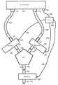
図5は、被測定デバイス(DUT)115を試験するように構成されたデバイステスター111、校正(cal)ポッド119、校正(cal)ポッド129、及び校正(cal)ポッド139を示す簡易ブロック図である。デバイステスター111は、例えば高周波(RF)ネットワークアナライザ、又はマイクロ波ベクトルネットワークアナライザ(VNA)である。 FIG. 5 is a simplified block diagram illustrating a
校正ポッド119の第1のポート120は、DUT115の第1のポート118に接続される。校正ポッド119の第2のポート121は、接続されていない。校正ポッド119のUSBポート122は、ケーブル128によりUSBハブ144に接続される。USBハブ144は、USBケーブル125によりデバイステスター111のUSBポート114にも接続される。 The
校正ポッド129の第1のポート130は、DUT115の第2のポート116に接続される。校正ポッド129の第2のポート131は、ケーブル123を介してデバイステスター111の第1のポート112(ポート1)に接続される。校正ポッド129のUSBポート132は、ケーブル133によりUSBハブ144に接続される。 The
校正ポッド139の第1のポート140は、DUT115の第3のポート117に接続される。校正ポッド139の第2のポート141は、ケーブル124を介してデバイステスター111の第2のポート113(ポート2)へ接続される。校正ポッド139のUSBポート142は、ケーブル143によりUSBハブ144に接続される。 The
USBプロトコルは、校正ポッド119、129、139とデバイステスター111との間の通信に使用される。代案として、ワイヤ接続、光接続、及び/又は無線接続の任意の多くの利用可能なタイプのプロトコルを通信に使用することもできる。 The USB protocol is used for communication between the
校正ポッド129は、デバイステスター111の第1のポート112(ポート1)で1ポート校正を実行する。校正ポッド139は、デバイステスター111の第2のポート113(ポート2)で1ポート校正を実行する。1ポート校正が完了すると、校正ポッド129と校正ポッド139のためのスルー経路をオンにし、校正がDUT115と校正ポッド129及び校正ポッド139の接合面へ変換される。 The
校正ポッド119は、インピーダンス終端状態に設定される。第2のポート116から第3のポート117へのDUT115のスルー経路が測定される。次に、「未知のスルー」校正を(上述したように)使用して、第2のポート116と第3のポート117との間のDUT115に関する全2ポート誤差補正項を得る。上述したように、三組の誤差補正済み2ポート測定値がDUT115に役立つ。それぞれの組は、校正ポッド119により提供されるように、DUT115のポート118における異なるインピーダンス設定からなる。三組の誤差補正済み2ポート測定値から、上述したようにDUT115の3ポートSパラメータを算出する。 The
図6は、校正ポッド119の簡易ブロック図である。校正ポッド129と校正ポッド139は、例えば設計において等価である。 FIG. 6 is a simplified block diagram of the
マイクロコントローラ233は、USBポート122に接続されたUSBポート回路232を介してデバイステスター111と通信する。コントローラ233用のプログラムは、ファームウェア231として格納される。メモリ236は、Sパラメータメモリ、電力(パワー)検出メモリ、ノイズ源メモリ、及びユーザーメモリを含む。Sパラメータメモリは校正ポッド119の特性記述を格納し、校正ポッド119をデバイステスター111に接続した際に、この特性記述を校正モジュール119がデバイステスター111に対して利用可能にする。電力検出メモリは、校正ポッド119に関する電力の特性記述の値を任意に格納するために使用される。ノイズ源メモリは、校正ポッド119に関するノイズ源の特性記述の値を任意に格納するために使用される。ユーザメモリは、システムのユーザにより利用されることができ、Sパラメータメモリ、電力検出メモリ、及びノイズ源メモリ内の値に加えて、又はそれらの代わりに使用され得る特性記述の値を格納することができる。 The
例えば、メモリ236はフラッシュメモリからなる。代案として、メモリ236は、別のタイプのコンピュータ読み取り可能な不揮発性メモリ(例えば、読み出し専用メモリ、プログラマブルROM、EPROM、EEPROM等)、又はコンピュータ読み取り可能な揮発性メモリ(例えば、ランダムアクセスメモリ、スタティックRAM、ダイナミックRAM等)からなる。 For example, the
コントローラ233からメモリ236へのデータ経路は、バススイッチ(SW)234とラッチ235を介して延びている。制御信号とアドレス信号は、コントローラ233からの命令を介して選択デコーダ237により生成される。選択デコーダ237は、ラッチ238とドライバ239を介してマルチステート回路243へ命令を供給する。マルチステート回路243は、校正ポッド119のポート120と121に接続される。マルチステート回路243が、ポート120とポート121で開放、短絡、スルー、及び負荷の校正標準の配置を制御する。 The data path from the
上記の説明は、本発明の例示的な方法および実施形態を単に開示して説明している。当事者には理解されるように、本発明はその思想または本質的な特徴から逸脱することなく他の具体的な形態で具現化され得る。従って、本発明の開示は、例示を意図したものであって、特許請求の範囲に記載された本発明の範囲を限定するものではない。 The foregoing description merely discloses and describes exemplary methods and embodiments of the present invention. As will be appreciated by those skilled in the art, the present invention may be embodied in other specific forms without departing from its spirit or essential characteristics. Accordingly, the disclosure of the present invention is intended to be illustrative and is not intended to limit the scope of the invention as recited in the claims.
11、111 デバイステスター
12、13、16-18、20、21、31-33、112、113、116-118、120、121 ポート
14、114 通信ポート
15、30、115 被測定デバイス(DUT)
19、119 校正モジュール
22、122 USBポート
30 方向性結合器
43 コントローラ
44 メモリ
45 ポート回路
11, 111 device tester
12, 13, 16-18, 20, 21, 31-33, 112, 113, 116-118, 120, 121 ports
14, 114 Communication port
15, 30, 115 Device under test (DUT)
19, 119 Calibration module
22, 122 USB port
30 Directional coupler
43 Controller
44 memory
45 port circuit
Claims (6)
Translated fromJapanese第1のポートと、
第2のポートと、
通信ポートとを含み、
前記デバイステスターが前記通信ポートを介して校正モジュールと通信し、前記被測定デバイスの第1のポートから前記校正モジュールのポートを物理的に切り離すことなく前記校正モジュールのポートにおける終端値を変更するように、前記校正モジュールに命令し、その命令は、前記被測定デバイスの第2のポートが前記デバイステスターの前記第1のポートに接続され、且つ前記被測定デバイスの第3のポートが前記デバイステスターの第2のポートに接続されて、前記デバイステスターが前記被測定デバイスの校正パラメータを取得する前記被測定デバイスの試験中に、与えられる、デバイステスター。The device under test adevice tester thattry trial,
And thefirstport,
And asecondport,
Including communication ports,
The device tester communicates with the calibration module via the communication portto change the termination value at the calibration module port without physically disconnecting the calibration module port from the first port of the device under test.And instructing the calibration module such that a second port of the device under test is connected to the first port of the device tester and a third port of the device under test is connected to the device tester. A device tester connected to a second port of the device to be provided during testing of the device under test to obtain calibration parameters of the device under test .
前記被測定デバイスの第1のポートが、前記パワースプリッタの入力ポートであり、及び
前記被測定デバイスの第2のポート及び第3のポートが、前記パワースプリッタの出力ポートである、請求項1に記載のデバイステスター。The device under test is a power splitter;
The first port of the device under test is an input port of the power splitter, and the second port and the third port of the device under test are output ports of the power splitter. Thedevice tester described.
前記被測定デバイスの第1のポートが、前記方向性結合器の出力ポートであり、及び
前記被測定デバイスの第2のポート及び第3のポートが、前記方向性結合器の被結合ポートである、請求項1に記載のデバイステスター。The device under test is a directional coupler;
The first port of the device under test is an output port of the directional coupler, and the second port and the third port of the device under test are coupled ports of the directional coupler. Thedevice tester according to claim 1.
前記被測定デバイスの第1のポートから前記被測定デバイスの第1のポートへの反射信号を表わすS11と、
前記被測定デバイスの第1のポートから前記被測定デバイスの第2のポートへの伝送信号を表わすS21と
前記被測定デバイスの第1のポートから前記被測定デバイスの第3のポートへの伝送信号を表わすS31と
前記被測定デバイスの第2のポートから前記被測定デバイスの第1のポートへの伝送信号を表わすS12と
前記被測定デバイスの第2のポートから前記被測定デバイスの第2のポートへの反射信号を表わすS22と、
前記被測定デバイスの第2のポートから前記被測定デバイスの第3のポートへの伝送信号を表わすS32と、
前記被測定デバイスの第3のポートから前記被測定デバイスの第1のポートへの伝送信号を表わすS13と、
前記被測定デバイスの第3のポートから前記被測定デバイスの第2のポートへの伝送信号を表わすS23と、及び
前記被測定デバイスの第3のポートから前記被測定デバイスの第3のポートへの反射信号を表わすS33とであり、
S21=S12、S13=S31、及びS23=S32である、請求項1に記載のデバイステスター。The calibration parameters are the following 3 port S parameters:
S11 representing a reflected signal from the first port of the device under test to the first port of the device under test;
S21 representing a transmission signal from the first port of the device under measurement to the second port of the device under measurement, and transmission from the first port of the device under measurement to the third port of the device under measurement the signal from the second port of the device under test and S12 representing the transmission signal from the second port of the device under test and S31 to the first port of the device under test representing the said measured device S22 representing the reflected signal to the two ports;
S32 representing a transmission signal from the second port of the device under test to the third port of the device under test;
S13 representing a transmission signal from the third port of the device under test to the first port of the device under test;
Wherein the S23 representing the transmission signal from the third port of the device under test to the second port of the device under test, and the to the third port of the device under test from the third port of the device under test S33 representing the reflected signal of
Thedevice tester according to claim 1, wherein S21 = S12 , S13 = S31 , and S23 = S32 .
Applications Claiming Priority (1)
| Application Number | Priority Date | Filing Date | Title |
|---|---|---|---|
| US10/712,645US7013229B2 (en) | 2003-11-13 | 2003-11-13 | Obtaining calibration parameters for a three-port device under test |
Publications (2)
| Publication Number | Publication Date |
|---|---|
| JP2005148067A JP2005148067A (en) | 2005-06-09 |
| JP4177804B2true JP4177804B2 (en) | 2008-11-05 |
Family
ID=34573588
Family Applications (1)
| Application Number | Title | Priority Date | Filing Date |
|---|---|---|---|
| JP2004328624AExpired - Fee RelatedJP4177804B2 (en) | 2003-11-13 | 2004-11-12 | Acquisition of calibration parameters for 3-port devices under test |
Country Status (2)
| Country | Link |
|---|---|
| US (1) | US7013229B2 (en) |
| JP (1) | JP4177804B2 (en) |
Families Citing this family (11)
| Publication number | Priority date | Publication date | Assignee | Title |
|---|---|---|---|---|
| US7002335B2 (en)* | 2004-05-24 | 2006-02-21 | Agilent Technologies, Inc. | Method for measuring a three-port device using a two-port vector network analyzer |
| US7170297B1 (en)* | 2006-03-20 | 2007-01-30 | Agilent Technologies, Inc. | Transmission response measurement system and method of using time gating |
| US7777497B2 (en)* | 2008-01-17 | 2010-08-17 | Com Dev International Ltd. | Method and system for tracking scattering parameter test system calibration |
| US8319502B2 (en)* | 2008-06-26 | 2012-11-27 | Dune Medical Devices Ltd. | RF calibration device and method |
| US8912809B2 (en)* | 2012-06-12 | 2014-12-16 | Apple Inc. | Methods and apparatus for performing wafer-level testing on antenna tuning elements |
| DE102013226065B4 (en) | 2013-12-16 | 2020-06-18 | Rohde & Schwarz GmbH & Co. Kommanditgesellschaft | Method for the controlled connection of a calibration standard in a calibration module and an associated calibration module |
| DE102016206104A1 (en)* | 2016-04-12 | 2017-10-12 | Rohde & Schwarz Gmbh & Co. Kg | Inline calibration module, program-controlled device and calibration and measuring system |
| US10901017B2 (en) | 2017-08-09 | 2021-01-26 | Nvidia Corporation | Systematic methodology to remove reflections from I/O measurements |
| CN112098792B (en)* | 2020-08-14 | 2023-02-28 | 中国电子科技集团公司第十三研究所 | Two-port on-chip calibration module model and method for parameter determination |
| US12078656B2 (en)* | 2020-09-11 | 2024-09-03 | National Technology & Engineering Solutions Of Sandia, Llc | Two-terminator RF adapter for background/environment noise measurement |
| CN119269853A (en)* | 2024-09-20 | 2025-01-07 | 武汉衍熙微器件有限公司 | Test Method |
Family Cites Families (12)
| Publication number | Priority date | Publication date | Assignee | Title |
|---|---|---|---|---|
| US5434511A (en)* | 1993-05-24 | 1995-07-18 | Atn Microwave, Inc. | Electronic microwave calibration device |
| US5467021A (en)* | 1993-05-24 | 1995-11-14 | Atn Microwave, Inc. | Calibration method and apparatus |
| US5587934A (en)* | 1993-10-21 | 1996-12-24 | Wiltron Company | Automatic VNA calibration apparatus |
| JP2807177B2 (en)* | 1994-07-27 | 1998-10-08 | 日本ヒューレット・パッカード株式会社 | Circuit network measuring device and calibration method |
| US5548538A (en)* | 1994-12-07 | 1996-08-20 | Wiltron Company | Internal automatic calibrator for vector network analyzers |
| US6333931B1 (en)* | 1998-12-28 | 2001-12-25 | Cisco Technology, Inc. | Method and apparatus for interconnecting a circuit-switched telephony network and a packet-switched data network, and applications thereof |
| US6421624B1 (en)* | 1999-02-05 | 2002-07-16 | Advantest Corp. | Multi-port device analysis apparatus and method and calibration method thereof |
| US6417674B1 (en)* | 2000-03-06 | 2002-07-09 | Agilent Technologies, Inc. | Two port self-calibration for an N-port network analyzer |
| US6614237B2 (en)* | 2000-09-18 | 2003-09-02 | Agilent Technologies, Inc. | Multiport automatic calibration device for a multiport test system |
| US6744262B2 (en)* | 2002-03-14 | 2004-06-01 | Agilent Technologies, Inc. | Method, apparatus, and article of manufacture for characterizing a device and predicting electrical behavior of the device in a circuit |
| US6757625B2 (en)* | 2002-04-22 | 2004-06-29 | Agilent Technologies, Inc. | Method, apparatus, and article of manufacture for predicting electrical behavior of a multiport device having balanced device ports |
| US6853198B2 (en)* | 2002-11-14 | 2005-02-08 | Agilent Technologies, Inc. | Method and apparatus for performing multiport through-reflect-line calibration and measurement |
- 2003
- 2003-11-13USUS10/712,645patent/US7013229B2/ennot_activeExpired - Fee Related
- 2004
- 2004-11-12JPJP2004328624Apatent/JP4177804B2/ennot_activeExpired - Fee Related
Also Published As
| Publication number | Publication date |
|---|---|
| US20050107972A1 (en) | 2005-05-19 |
| US7013229B2 (en) | 2006-03-14 |
| JP2005148067A (en) | 2005-06-09 |
Similar Documents
| Publication | Publication Date | Title |
|---|---|---|
| US12320882B2 (en) | Integrated vector network analyzer | |
| US6853198B2 (en) | Method and apparatus for performing multiport through-reflect-line calibration and measurement | |
| US7256585B1 (en) | Match-corrected power measurements with a vector network analyzer | |
| US10969421B2 (en) | Integrated vector network analyzer | |
| US6188968B1 (en) | Removing effects of adapters present during vector network analyzer calibration | |
| US6060888A (en) | Error correction method for reflection measurements of reciprocal devices in vector network analyzers | |
| US8860434B2 (en) | Method of measuring scattering parameters of device under test | |
| US6836743B1 (en) | Compensating for unequal load and source match in vector network analyzer calibration | |
| US20050030047A1 (en) | Method and apparatus for measuring a device under test using an improved through-reflect-line measurement calibration | |
| US6417674B1 (en) | Two port self-calibration for an N-port network analyzer | |
| US20040251922A1 (en) | Methods and computer program products for full N-port vector network analyzer calibrations | |
| JP2004317506A (en) | Characterization of balanced device including test system calibration | |
| US20080204039A1 (en) | Self Calibration Apparatus And Methods | |
| US20100318833A1 (en) | Method for the secondary error correction of a multi-port network analyzer | |
| JPH11118853A (en) | Automatic calibration of network analyzer | |
| US20110199107A1 (en) | Method and apparatus for calibrating a test system for measuring a device under test | |
| JP4177804B2 (en) | Acquisition of calibration parameters for 3-port devices under test | |
| US20170234959A1 (en) | Calibration apparatus and method for network analyzer | |
| US20130317767A1 (en) | Measurement error correction method and electronic component characteristic measurement apparatus | |
| CN113359078A (en) | Vector network analyzer calibration method based on sixteen-term error model | |
| US6965241B1 (en) | Automated electronic calibration apparatus | |
| US7030625B1 (en) | Method and apparatus for performing a minimum connection multiport through-reflect-line calibration and measurement | |
| US7088087B2 (en) | Network analyzer including automatic port extension calibration and method of operation | |
| US11054450B2 (en) | Method of calibrating a measurement and analyzing device as well as method of measuring a frequency-converting device under test | |
| US20080010034A1 (en) | Method for network analyzer calibration and network analyzer |
Legal Events
| Date | Code | Title | Description |
|---|---|---|---|
| A131 | Notification of reasons for refusal | Free format text:JAPANESE INTERMEDIATE CODE: A131 Effective date:20071127 | |
| A521 | Written amendment | Free format text:JAPANESE INTERMEDIATE CODE: A523 Effective date:20080226 | |
| TRDD | Decision of grant or rejection written | ||
| A01 | Written decision to grant a patent or to grant a registration (utility model) | Free format text:JAPANESE INTERMEDIATE CODE: A01 Effective date:20080722 | |
| A01 | Written decision to grant a patent or to grant a registration (utility model) | Free format text:JAPANESE INTERMEDIATE CODE: A01 | |
| A61 | First payment of annual fees (during grant procedure) | Free format text:JAPANESE INTERMEDIATE CODE: A61 Effective date:20080822 | |
| FPAY | Renewal fee payment (event date is renewal date of database) | Free format text:PAYMENT UNTIL: 20110829 Year of fee payment:3 | |
| R150 | Certificate of patent or registration of utility model | Free format text:JAPANESE INTERMEDIATE CODE: R150 | |
| LAPS | Cancellation because of no payment of annual fees |