JP4175826B2 - Liquid crystal display - Google Patents
Liquid crystal displayDownload PDFInfo
- Publication number
- JP4175826B2 JP4175826B2JP2002113972AJP2002113972AJP4175826B2JP 4175826 B2JP4175826 B2JP 4175826B2JP 2002113972 AJP2002113972 AJP 2002113972AJP 2002113972 AJP2002113972 AJP 2002113972AJP 4175826 B2JP4175826 B2JP 4175826B2
- Authority
- JP
- Japan
- Prior art keywords
- liquid crystal
- crystal display
- display device
- monomer
- substrates
- Prior art date
- Legal status (The legal status is an assumption and is not a legal conclusion. Google has not performed a legal analysis and makes no representation as to the accuracy of the status listed.)
- Expired - Lifetime
Links
Images

Classifications
- C—CHEMISTRY; METALLURGY
- C09—DYES; PAINTS; POLISHES; NATURAL RESINS; ADHESIVES; COMPOSITIONS NOT OTHERWISE PROVIDED FOR; APPLICATIONS OF MATERIALS NOT OTHERWISE PROVIDED FOR
- C09K—MATERIALS FOR MISCELLANEOUS APPLICATIONS, NOT PROVIDED FOR ELSEWHERE
- C09K19/00—Liquid crystal materials
- C09K19/04—Liquid crystal materials characterised by the chemical structure of the liquid crystal components, e.g. by a specific unit
- C09K19/06—Non-steroidal liquid crystal compounds
- C09K19/08—Non-steroidal liquid crystal compounds containing at least two non-condensed rings
- C09K19/10—Non-steroidal liquid crystal compounds containing at least two non-condensed rings containing at least two benzene rings
- C09K19/12—Non-steroidal liquid crystal compounds containing at least two non-condensed rings containing at least two benzene rings at least two benzene rings directly linked, e.g. biphenyls
- G—PHYSICS
- G02—OPTICS
- G02F—OPTICAL DEVICES OR ARRANGEMENTS FOR THE CONTROL OF LIGHT BY MODIFICATION OF THE OPTICAL PROPERTIES OF THE MEDIA OF THE ELEMENTS INVOLVED THEREIN; NON-LINEAR OPTICS; FREQUENCY-CHANGING OF LIGHT; OPTICAL LOGIC ELEMENTS; OPTICAL ANALOGUE/DIGITAL CONVERTERS
- G02F1/00—Devices or arrangements for the control of the intensity, colour, phase, polarisation or direction of light arriving from an independent light source, e.g. switching, gating or modulating; Non-linear optics
- G02F1/01—Devices or arrangements for the control of the intensity, colour, phase, polarisation or direction of light arriving from an independent light source, e.g. switching, gating or modulating; Non-linear optics for the control of the intensity, phase, polarisation or colour
- G02F1/13—Devices or arrangements for the control of the intensity, colour, phase, polarisation or direction of light arriving from an independent light source, e.g. switching, gating or modulating; Non-linear optics for the control of the intensity, phase, polarisation or colour based on liquid crystals, e.g. single liquid crystal display cells
- C—CHEMISTRY; METALLURGY
- C08—ORGANIC MACROMOLECULAR COMPOUNDS; THEIR PREPARATION OR CHEMICAL WORKING-UP; COMPOSITIONS BASED THEREON
- C08F—MACROMOLECULAR COMPOUNDS OBTAINED BY REACTIONS ONLY INVOLVING CARBON-TO-CARBON UNSATURATED BONDS
- C08F2/00—Processes of polymerisation
- C—CHEMISTRY; METALLURGY
- C09—DYES; PAINTS; POLISHES; NATURAL RESINS; ADHESIVES; COMPOSITIONS NOT OTHERWISE PROVIDED FOR; APPLICATIONS OF MATERIALS NOT OTHERWISE PROVIDED FOR
- C09K—MATERIALS FOR MISCELLANEOUS APPLICATIONS, NOT PROVIDED FOR ELSEWHERE
- C09K19/00—Liquid crystal materials
- C09K19/04—Liquid crystal materials characterised by the chemical structure of the liquid crystal components, e.g. by a specific unit
- C09K19/06—Non-steroidal liquid crystal compounds
- C09K19/08—Non-steroidal liquid crystal compounds containing at least two non-condensed rings
- C09K19/10—Non-steroidal liquid crystal compounds containing at least two non-condensed rings containing at least two benzene rings
- C09K19/20—Non-steroidal liquid crystal compounds containing at least two non-condensed rings containing at least two benzene rings linked by a chain containing carbon and oxygen atoms as chain links, e.g. esters or ethers
- C09K19/2007—Non-steroidal liquid crystal compounds containing at least two non-condensed rings containing at least two benzene rings linked by a chain containing carbon and oxygen atoms as chain links, e.g. esters or ethers the chain containing -COO- or -OCO- groups
- C—CHEMISTRY; METALLURGY
- C09—DYES; PAINTS; POLISHES; NATURAL RESINS; ADHESIVES; COMPOSITIONS NOT OTHERWISE PROVIDED FOR; APPLICATIONS OF MATERIALS NOT OTHERWISE PROVIDED FOR
- C09K—MATERIALS FOR MISCELLANEOUS APPLICATIONS, NOT PROVIDED FOR ELSEWHERE
- C09K19/00—Liquid crystal materials
- C09K19/04—Liquid crystal materials characterised by the chemical structure of the liquid crystal components, e.g. by a specific unit
- C09K19/06—Non-steroidal liquid crystal compounds
- C09K19/32—Non-steroidal liquid crystal compounds containing condensed ring systems, i.e. fused, bridged or spiro ring systems
- C09K19/322—Compounds containing a naphthalene ring or a completely or partially hydrogenated naphthalene ring
- C—CHEMISTRY; METALLURGY
- C09—DYES; PAINTS; POLISHES; NATURAL RESINS; ADHESIVES; COMPOSITIONS NOT OTHERWISE PROVIDED FOR; APPLICATIONS OF MATERIALS NOT OTHERWISE PROVIDED FOR
- C09K—MATERIALS FOR MISCELLANEOUS APPLICATIONS, NOT PROVIDED FOR ELSEWHERE
- C09K19/00—Liquid crystal materials
- C09K19/04—Liquid crystal materials characterised by the chemical structure of the liquid crystal components, e.g. by a specific unit
- C09K19/06—Non-steroidal liquid crystal compounds
- C09K19/34—Non-steroidal liquid crystal compounds containing at least one heterocyclic ring
- C—CHEMISTRY; METALLURGY
- C09—DYES; PAINTS; POLISHES; NATURAL RESINS; ADHESIVES; COMPOSITIONS NOT OTHERWISE PROVIDED FOR; APPLICATIONS OF MATERIALS NOT OTHERWISE PROVIDED FOR
- C09K—MATERIALS FOR MISCELLANEOUS APPLICATIONS, NOT PROVIDED FOR ELSEWHERE
- C09K19/00—Liquid crystal materials
- C09K19/04—Liquid crystal materials characterised by the chemical structure of the liquid crystal components, e.g. by a specific unit
- C09K19/38—Polymers
- G—PHYSICS
- G02—OPTICS
- G02F—OPTICAL DEVICES OR ARRANGEMENTS FOR THE CONTROL OF LIGHT BY MODIFICATION OF THE OPTICAL PROPERTIES OF THE MEDIA OF THE ELEMENTS INVOLVED THEREIN; NON-LINEAR OPTICS; FREQUENCY-CHANGING OF LIGHT; OPTICAL LOGIC ELEMENTS; OPTICAL ANALOGUE/DIGITAL CONVERTERS
- G02F1/00—Devices or arrangements for the control of the intensity, colour, phase, polarisation or direction of light arriving from an independent light source, e.g. switching, gating or modulating; Non-linear optics
- G02F1/01—Devices or arrangements for the control of the intensity, colour, phase, polarisation or direction of light arriving from an independent light source, e.g. switching, gating or modulating; Non-linear optics for the control of the intensity, phase, polarisation or colour
- G02F1/13—Devices or arrangements for the control of the intensity, colour, phase, polarisation or direction of light arriving from an independent light source, e.g. switching, gating or modulating; Non-linear optics for the control of the intensity, phase, polarisation or colour based on liquid crystals, e.g. single liquid crystal display cells
- G02F1/133—Constructional arrangements; Operation of liquid crystal cells; Circuit arrangements
- G02F1/1333—Constructional arrangements; Manufacturing methods
- G02F1/133365—Cells in which the active layer comprises a liquid crystalline polymer
- G—PHYSICS
- G02—OPTICS
- G02F—OPTICAL DEVICES OR ARRANGEMENTS FOR THE CONTROL OF LIGHT BY MODIFICATION OF THE OPTICAL PROPERTIES OF THE MEDIA OF THE ELEMENTS INVOLVED THEREIN; NON-LINEAR OPTICS; FREQUENCY-CHANGING OF LIGHT; OPTICAL LOGIC ELEMENTS; OPTICAL ANALOGUE/DIGITAL CONVERTERS
- G02F1/00—Devices or arrangements for the control of the intensity, colour, phase, polarisation or direction of light arriving from an independent light source, e.g. switching, gating or modulating; Non-linear optics
- G02F1/01—Devices or arrangements for the control of the intensity, colour, phase, polarisation or direction of light arriving from an independent light source, e.g. switching, gating or modulating; Non-linear optics for the control of the intensity, phase, polarisation or colour
- G02F1/13—Devices or arrangements for the control of the intensity, colour, phase, polarisation or direction of light arriving from an independent light source, e.g. switching, gating or modulating; Non-linear optics for the control of the intensity, phase, polarisation or colour based on liquid crystals, e.g. single liquid crystal display cells
- G02F1/133—Constructional arrangements; Operation of liquid crystal cells; Circuit arrangements
- G02F1/1333—Constructional arrangements; Manufacturing methods
- G02F1/1337—Surface-induced orientation of the liquid crystal molecules, e.g. by alignment layers
- G02F1/13378—Surface-induced orientation of the liquid crystal molecules, e.g. by alignment layers by treatment of the surface, e.g. embossing, rubbing or light irradiation
- G02F1/133788—Surface-induced orientation of the liquid crystal molecules, e.g. by alignment layers by treatment of the surface, e.g. embossing, rubbing or light irradiation by light irradiation, e.g. linearly polarised light photo-polymerisation
- G—PHYSICS
- G02—OPTICS
- G02F—OPTICAL DEVICES OR ARRANGEMENTS FOR THE CONTROL OF LIGHT BY MODIFICATION OF THE OPTICAL PROPERTIES OF THE MEDIA OF THE ELEMENTS INVOLVED THEREIN; NON-LINEAR OPTICS; FREQUENCY-CHANGING OF LIGHT; OPTICAL LOGIC ELEMENTS; OPTICAL ANALOGUE/DIGITAL CONVERTERS
- G02F1/00—Devices or arrangements for the control of the intensity, colour, phase, polarisation or direction of light arriving from an independent light source, e.g. switching, gating or modulating; Non-linear optics
- G02F1/01—Devices or arrangements for the control of the intensity, colour, phase, polarisation or direction of light arriving from an independent light source, e.g. switching, gating or modulating; Non-linear optics for the control of the intensity, phase, polarisation or colour
- G02F1/13—Devices or arrangements for the control of the intensity, colour, phase, polarisation or direction of light arriving from an independent light source, e.g. switching, gating or modulating; Non-linear optics for the control of the intensity, phase, polarisation or colour based on liquid crystals, e.g. single liquid crystal display cells
- G02F1/137—Devices or arrangements for the control of the intensity, colour, phase, polarisation or direction of light arriving from an independent light source, e.g. switching, gating or modulating; Non-linear optics for the control of the intensity, phase, polarisation or colour based on liquid crystals, e.g. single liquid crystal display cells characterised by the electro-optical or magneto-optical effect, e.g. field-induced phase transition, orientation effect, guest-host interaction or dynamic scattering
- G02F1/139—Devices or arrangements for the control of the intensity, colour, phase, polarisation or direction of light arriving from an independent light source, e.g. switching, gating or modulating; Non-linear optics for the control of the intensity, phase, polarisation or colour based on liquid crystals, e.g. single liquid crystal display cells characterised by the electro-optical or magneto-optical effect, e.g. field-induced phase transition, orientation effect, guest-host interaction or dynamic scattering based on orientation effects in which the liquid crystal remains transparent
- G02F1/1393—Devices or arrangements for the control of the intensity, colour, phase, polarisation or direction of light arriving from an independent light source, e.g. switching, gating or modulating; Non-linear optics for the control of the intensity, phase, polarisation or colour based on liquid crystals, e.g. single liquid crystal display cells characterised by the electro-optical or magneto-optical effect, e.g. field-induced phase transition, orientation effect, guest-host interaction or dynamic scattering based on orientation effects in which the liquid crystal remains transparent the birefringence of the liquid crystal being electrically controlled, e.g. ECB-, DAP-, HAN-, PI-LC cells
- C—CHEMISTRY; METALLURGY
- C09—DYES; PAINTS; POLISHES; NATURAL RESINS; ADHESIVES; COMPOSITIONS NOT OTHERWISE PROVIDED FOR; APPLICATIONS OF MATERIALS NOT OTHERWISE PROVIDED FOR
- C09K—MATERIALS FOR MISCELLANEOUS APPLICATIONS, NOT PROVIDED FOR ELSEWHERE
- C09K19/00—Liquid crystal materials
- C09K19/04—Liquid crystal materials characterised by the chemical structure of the liquid crystal components, e.g. by a specific unit
- C09K2019/0444—Liquid crystal materials characterised by the chemical structure of the liquid crystal components, e.g. by a specific unit characterized by a linking chain between rings or ring systems, a bridging chain between extensive mesogenic moieties or an end chain group
- C09K2019/0448—Liquid crystal materials characterised by the chemical structure of the liquid crystal components, e.g. by a specific unit characterized by a linking chain between rings or ring systems, a bridging chain between extensive mesogenic moieties or an end chain group the end chain group being a polymerizable end group, e.g. -Sp-P or acrylate
- C—CHEMISTRY; METALLURGY
- C09—DYES; PAINTS; POLISHES; NATURAL RESINS; ADHESIVES; COMPOSITIONS NOT OTHERWISE PROVIDED FOR; APPLICATIONS OF MATERIALS NOT OTHERWISE PROVIDED FOR
- C09K—MATERIALS FOR MISCELLANEOUS APPLICATIONS, NOT PROVIDED FOR ELSEWHERE
- C09K19/00—Liquid crystal materials
- C09K19/52—Liquid crystal materials characterised by components which are not liquid crystals, e.g. additives with special physical aspect: solvents, solid particles
- C09K19/54—Additives having no specific mesophase characterised by their chemical composition
- C09K19/542—Macromolecular compounds
- C09K2019/548—Macromolecular compounds stabilizing the alignment; Polymer stabilized alignment
- C—CHEMISTRY; METALLURGY
- C09—DYES; PAINTS; POLISHES; NATURAL RESINS; ADHESIVES; COMPOSITIONS NOT OTHERWISE PROVIDED FOR; APPLICATIONS OF MATERIALS NOT OTHERWISE PROVIDED FOR
- C09K—MATERIALS FOR MISCELLANEOUS APPLICATIONS, NOT PROVIDED FOR ELSEWHERE
- C09K2323/00—Functional layers of liquid crystal optical display excluding electroactive liquid crystal layer characterised by chemical composition
- C09K2323/03—Viewing layer characterised by chemical composition
- G—PHYSICS
- G02—OPTICS
- G02F—OPTICAL DEVICES OR ARRANGEMENTS FOR THE CONTROL OF LIGHT BY MODIFICATION OF THE OPTICAL PROPERTIES OF THE MEDIA OF THE ELEMENTS INVOLVED THEREIN; NON-LINEAR OPTICS; FREQUENCY-CHANGING OF LIGHT; OPTICAL LOGIC ELEMENTS; OPTICAL ANALOGUE/DIGITAL CONVERTERS
- G02F1/00—Devices or arrangements for the control of the intensity, colour, phase, polarisation or direction of light arriving from an independent light source, e.g. switching, gating or modulating; Non-linear optics
- G02F1/01—Devices or arrangements for the control of the intensity, colour, phase, polarisation or direction of light arriving from an independent light source, e.g. switching, gating or modulating; Non-linear optics for the control of the intensity, phase, polarisation or colour
- G02F1/13—Devices or arrangements for the control of the intensity, colour, phase, polarisation or direction of light arriving from an independent light source, e.g. switching, gating or modulating; Non-linear optics for the control of the intensity, phase, polarisation or colour based on liquid crystals, e.g. single liquid crystal display cells
- G02F1/133—Constructional arrangements; Operation of liquid crystal cells; Circuit arrangements
- G02F1/1333—Constructional arrangements; Manufacturing methods
- G02F1/133397—Constructional arrangements; Manufacturing methods for suppressing after-image or image-sticking
- G—PHYSICS
- G02—OPTICS
- G02F—OPTICAL DEVICES OR ARRANGEMENTS FOR THE CONTROL OF LIGHT BY MODIFICATION OF THE OPTICAL PROPERTIES OF THE MEDIA OF THE ELEMENTS INVOLVED THEREIN; NON-LINEAR OPTICS; FREQUENCY-CHANGING OF LIGHT; OPTICAL LOGIC ELEMENTS; OPTICAL ANALOGUE/DIGITAL CONVERTERS
- G02F1/00—Devices or arrangements for the control of the intensity, colour, phase, polarisation or direction of light arriving from an independent light source, e.g. switching, gating or modulating; Non-linear optics
- G02F1/01—Devices or arrangements for the control of the intensity, colour, phase, polarisation or direction of light arriving from an independent light source, e.g. switching, gating or modulating; Non-linear optics for the control of the intensity, phase, polarisation or colour
- G02F1/13—Devices or arrangements for the control of the intensity, colour, phase, polarisation or direction of light arriving from an independent light source, e.g. switching, gating or modulating; Non-linear optics for the control of the intensity, phase, polarisation or colour based on liquid crystals, e.g. single liquid crystal display cells
- G02F1/133—Constructional arrangements; Operation of liquid crystal cells; Circuit arrangements
- G02F1/1333—Constructional arrangements; Manufacturing methods
- G02F1/1337—Surface-induced orientation of the liquid crystal molecules, e.g. by alignment layers
- G02F1/133707—Structures for producing distorted electric fields, e.g. bumps, protrusions, recesses, slits in pixel electrodes
- G—PHYSICS
- G02—OPTICS
- G02F—OPTICAL DEVICES OR ARRANGEMENTS FOR THE CONTROL OF LIGHT BY MODIFICATION OF THE OPTICAL PROPERTIES OF THE MEDIA OF THE ELEMENTS INVOLVED THEREIN; NON-LINEAR OPTICS; FREQUENCY-CHANGING OF LIGHT; OPTICAL LOGIC ELEMENTS; OPTICAL ANALOGUE/DIGITAL CONVERTERS
- G02F1/00—Devices or arrangements for the control of the intensity, colour, phase, polarisation or direction of light arriving from an independent light source, e.g. switching, gating or modulating; Non-linear optics
- G02F1/01—Devices or arrangements for the control of the intensity, colour, phase, polarisation or direction of light arriving from an independent light source, e.g. switching, gating or modulating; Non-linear optics for the control of the intensity, phase, polarisation or colour
- G02F1/13—Devices or arrangements for the control of the intensity, colour, phase, polarisation or direction of light arriving from an independent light source, e.g. switching, gating or modulating; Non-linear optics for the control of the intensity, phase, polarisation or colour based on liquid crystals, e.g. single liquid crystal display cells
- G02F1/137—Devices or arrangements for the control of the intensity, colour, phase, polarisation or direction of light arriving from an independent light source, e.g. switching, gating or modulating; Non-linear optics for the control of the intensity, phase, polarisation or colour based on liquid crystals, e.g. single liquid crystal display cells characterised by the electro-optical or magneto-optical effect, e.g. field-induced phase transition, orientation effect, guest-host interaction or dynamic scattering
- G02F1/13775—Polymer-stabilized liquid crystal layers
Landscapes
- Chemical & Material Sciences (AREA)
- Physics & Mathematics (AREA)
- Crystallography & Structural Chemistry (AREA)
- Nonlinear Science (AREA)
- Organic Chemistry (AREA)
- Engineering & Computer Science (AREA)
- Materials Engineering (AREA)
- Optics & Photonics (AREA)
- General Physics & Mathematics (AREA)
- Mathematical Physics (AREA)
- Spectroscopy & Molecular Physics (AREA)
- Polymers & Plastics (AREA)
- Medicinal Chemistry (AREA)
- Chemical Kinetics & Catalysis (AREA)
- Health & Medical Sciences (AREA)
- Liquid Crystal (AREA)
- Addition Polymer Or Copolymer, Post-Treatments, Or Chemical Modifications (AREA)
- Liquid Crystal Substances (AREA)
- Polymerisation Methods In General (AREA)
Description
Translated fromJapanese【0001】
【発明の属する技術分野】
本発明は、光又は熱により重合するモノマーやオリゴマーなどを含有する液晶材料を基板間に封止し、液晶層に印加する電圧を調整しながら重合性成分を重合して液晶の配向方向を決定する液晶表示装置及び液晶材料に関する。前記電圧は0ボルトを含み、以下電圧調整とは0ボルトを含むものとする。
【0002】
【従来の技術】
アクティブマトリックスタイプの液晶表示装置は、以前はTN(twisted nematic)モードが主流であった。TNモードの場合、視角特性が狭いのが難点であった。そこで現在、広視野角液晶パネルには、MVA(multidomain vertical alignment)モードとIPS(In−Plane−Switching)モードと呼ばれる技術が採用されている。
【0003】
IPSモードでは、表示面方向に平行な水平面内に互いに対向する1組の平たい櫛形電極を設け、対向する電極間の液晶分子を水平面内でスイッチングする。平たい形状の櫛形電極は液晶表示装置の開口率を著しく低下させるので、IPSモード液晶表示装置では強力なバックライトが必要である。
【0004】
MVAモードでは、液晶を基板に垂直に配向させ、透明電極(ITO膜)に設けられたスリットと対向基板に設けられた突起によって液晶分子の配向を規定する。MVAモード液晶表示装置におけるスリットや突起による実質開口率の低下は櫛形電極を用いるIPSモード液晶表示装置におけるほどではないにしても、TNモード液晶表示装置に比べると、MVAモード液晶表示装置の光透過率は低い。そのため、MVAモード液晶表示装置は、低消費電力が要求されるノートパソコンには採用することができていない。
【0005】
最近のMVAモード液晶表示装置では、広視野角化のため、電圧印加時に液晶分子が4方向に倒れるよう、土手(突起)とITOスリットを複雑に配置しているため、光透過率が更に低くなっている。これらの配置を単純化し、土手間隔あるいはITOスリット間隙を広げれば、光透過率を高くすることができる。しかし、土手あるいはITOスリットの間隙が非常に広いと、液晶分子の傾斜の伝播に時間がかかるようになり、表示のため装置に電圧を印加したときの装置の応答が非常に遅くなる。
【0006】
この応答の遅れの問題の解決のために、MVAモード液晶表示装置の製造において、重合可能なモノマーを含有している液晶材料を基板間に注入し、電圧を印加した状態でモノマーを重合して液晶分子の倒れる方向を記憶しておくという技術が導入された。
【0007】
【発明が解決しようとする課題】
一般に、液晶表示装置には、同じ画像を長時間表示し続けると、表示画像を変えても前の画像が残って見えてしまう焼付き現象が、多かれ少なかれ認められる。重合可能なモノマーを含む液晶材料を基板間に注入し、電圧を印加した状態でモノマーを重合して液晶分子の倒れる方向を記憶しておくという上述の技術により製造した液晶表示装置においても、やはり焼付き現象の発生は避けて通れない問題であり、それを確実に低減できる技術はこれまで知られていないのが実状であった。
【0008】
そこで、本発明は、焼付きを効果的に低減した液晶表示装置、特にMVAモード液晶表示装置の提供を目的とするものである。
【0009】
【課題を解決するための手段】
本発明が提供する液晶表示装置は、透明電極と液晶分子を配向させる配向制御膜とを備えた2枚の基板を有し、これらの基板の間に液晶組成物を含んでなる液晶表示装置であり、重合可能なモノマーを含有している液晶組成物を2枚の基板の間に注入し、これらの基板の相対する透明電極の間に電圧を印加しながら、該モノマーを重合する工程を経て製造される液晶表示装置であって、上記液晶組成物中に含まれる重合可能なモノマーが、1つ以上の環構造あるいは縮環構造と、該環構造あるいは縮環構造と直接結合している2つの官能基とを有することを特徴とする液晶表示装置である。
【0010】
【発明の実施の形態】
本発明は、電圧印加時の応答の遅れを基板間に封入した液晶分子の倒れる方向を記憶しておくことにより改善した液晶表示装置における、いわゆる焼付き現象を、液晶分子の倒れる方向を規制するため液晶表示装置の製造段階で使用するモノマー化合物として特別なものを使用することにより大幅に低減したものである。
【0011】
具体的に言えば、本発明は、発明者らが液晶表示装置の焼付きの問題を解決するため、使用する各種モノマー化合物と液晶組成物について行った様々な検討の結果得た、以下の知見を基にしている。
液晶組成物中に含まれるモノマーの分子量が小さいほど、焼付きは少なくなる。
液晶組成物中に含まれるモノマーが環構造あるいは縮環構造と官能基を有し、且つ環構造と官能基が直接結合していると、焼付きが少なくなる。
環構造の数が1のモノマーより環構造2個が縮環したモノマーを使用する方が、環構造2個が縮環したモノマーより非縮環式の環構造2個のモノマーを使用する方が、焼付きが少なくなる。
【0012】
本発明において環構造あるいは縮環構造のモノマー化合物を使用するのは、官能基を持たない通常の液晶分子の方向とモノマーの分子方向とが揃うために必要である。使用するモノマーにおける環の数が1のモノマーより環構造2個が縮環したモノマーの方が、また、環構造2個が縮環したモノマーより非縮環式の環構造2個のモノマーの方が、通常の液晶分子を配向させる能力が高く、また、相対的に官能基部の分子中に占める割合が減り、分子そのものが剛直となる。一方、モノマーが環構造と官能基との間にアルキレン基あるいはポリメチレン基などの屈曲可能な部位を含むと、高分子化後、液晶表示装置に電圧を印加すると液晶分子とともに高分子も変形し、焼付きの原因になる。
【0013】
本発明で使用するモノマー化合物は、好ましくは、下記一般式(1)で表されるものから選ばれる。
P1−A1−(Z1−A2)n−P2 (1)
この式中、P1及びP2は官能基であって、それぞれ独立に、アクリレート、メタクリレート、ビニル、ビニロキシ又はエポキシ基であり、A1及びA2は環構造であって、それぞれ独立に、1,4−フェニレン又はナフタレン−2,6−ジイル基を表し、Z1は−COO−もしくは−OCO−基又は単結合であり、nは0、1又は2である。
【0014】
式(1)において、P1及びP2は好ましくはアクリレート基であり、Z1は好ましくは単結合であり、nは好ましくは0又は1である。本発明において殊に好ましいモノマーは、次の式で表される化合物である。
【0015】
【化5】
上式中、P1及びP2は先に式(1)において定義されたとおりであり、特に好ましいP1及びP2はアクリレート基である。
【0017】
上記の化合物のうちで非常に好ましいのは式(1a)及び(1b)の化合物であり、式(1a)の化合物が特に好ましい。
【0018】
【実施例】
次に、実施例により本発明を詳しく説明するが、本発明は以下の実施例に限定されるものではない。
【0019】
以下の例における液晶表示装置では、垂直配向膜を使用した。また、誘電率異方性が負の液晶を使用し、そして電圧無印加時の液晶分子のダイレクタが基板に対しておおよそ垂直方向になるようにした。偏光板はクロスニコルに液晶表示装置の両側に貼付するのでノーマリーブラックであり、偏光板の偏光軸はバスラインに対して平行であった。パネルサイズは15型、解像度はXGAであった。
【0020】
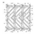
図1に、作製した液晶表示装置を説明する模式平面図を示し、図2に、図1のII−II線断面図を示す。一方のガラス基板16に、遮光用のブラックマトリクス34と色分解フィルタ(カラーフィルタ)39が形成され、色分解フィルタ39の上一面にITOの共通電極12が形成されている。ガラス基板16には、更にジグザグ状に突起20が形成され、また補助突起20’も形成されている。他方のガラス基板17には、複数本の平行なゲートバスライン31、ゲートバスライン31と垂直方向に平行に形成された複数本のデータバスライン32、ゲートバスライン31とデータバスライン32との交点に対応してマトリクス状に形成されれた薄膜トランジスタ(TFT)33、そしてITOの表示画素電極13が設けられている。ゲートバスライン31は、絶縁膜51によりデータバスライン32から切り離され、そしてデータバスライン32と同じ層にTFT33のソース・ドレイン電極が形成されている。データバスライン32の層上には絶縁膜52が形成され、更にその上に画素電極13が形成されている。画素電極13には、図1の平面図で突起20と平行に、且つ隣り合う突起20の中間の位置に、スリット21が設けられている。ゲートバスライン31と平行に、且つ隣り合うゲートバスライン31の中間の位置には、各画素電極13の電位を安定化するための補助容量用にCs電極35が設けられている。図2に見られるように、共通電極12と画素電極13とが対向するように2枚のガラス基板16、17を組み合わせ、それらの間に液晶組成物(図示せず)が保持される。共通電極12と画素電極13の表面には配向制御膜が形成されているが、簡単にするため、図2にこれらは図示していない。同様に、ガラス基板16、17のおのおのの外面側に貼付する偏光板も、簡単にするため、図2には図示していない。
【0021】
また、以下の例では、焼付き率を以下のようにして求めた。
白黒チェッカーパターンを表示領域に48時間表示させた。その後表示領域全域に所定の中間調(グレイ)を表示させ、白表示であった領域の輝度βと黒表示であった領域の輝度γとの差(β−γ)を、黒表示であった領域の輝度γで除して焼付き率を求めた。すなわち、焼付き率αを次の式で計算した。
焼付き率α=((β−γ)/γ)×100(%)
【0022】
(比較例1)
環構造と官能基の間にトリメチレン鎖を有し、分子量が比較的大きい、下式で表されるジアクリレート
【0023】
【化6】
を0.3wt%を加えた液晶組成物を、液晶表示装置の対向基板間に注入後、10Vの電圧を印加しながら、紫外線を室温で4J/cm2照射した。この液晶表示装置の48時間の焼付き率は25%であった。
【0025】
(比較例2)
環構造と官能基の間にヘキサメチレン鎖を有する、下式で表されるジアクリレート
【0026】
【化7】
を0.3wt%加えた液晶組成物を、液晶表示装置の対向基板間に注入後、10Vの電圧を印加しながら、紫外線を室温で4J/cm2照射した。この液晶表示装置の48時間の焼付き率は26%であった。
【0028】
(実施例1)
環構造と官能基が直接結合した、下式で表されるジアクリレート
【0029】
【化8】
を0.3wt%加えた液晶組成物を、液晶表示装置の対向基板間に注入後、10Vの電圧を印加しながら、紫外線を室温で4J/cm2照射した。この液晶表示装置の48時間の焼付き率は6%であった。
【0031】
【発明の効果】
以上説明したように、本発明によれば、焼付き率を大幅に低減した液晶表示装置の提供か可能になる。
【図面の簡単な説明】
【図1】比較例と実施例で作製した液晶表示装置を説明する模式平面図である。
【図2】図1のII−II線断面図である。
【符号の説明】
12…共通電極
13…画素電極
16、17…ガラス基板
20…突起
21…画素電極のスリット
31…ゲートバスライン
32…データバスライン
33…TFT
34…ブラックマトリクス
35…Cs電極[0001]
BACKGROUND OF THE INVENTION
In the present invention, a liquid crystal material containing a monomer or oligomer that is polymerized by light or heat is sealed between substrates, and a polymerizable component is polymerized while adjusting a voltage applied to the liquid crystal layer to determine the alignment direction of the liquid crystal. The present invention relates to a liquid crystal display device and a liquid crystal material. The voltage includes 0 volts, and the voltage adjustment hereinafter includes 0 volts.
[0002]
[Prior art]
In the past, active matrix type liquid crystal display devices were mainly in the TN (twisted nematic) mode. In the case of the TN mode, it is difficult to have a narrow viewing angle characteristic. Therefore, at present, technologies called an MVA (multidomain vertical alignment) mode and an IPS (In-Plane-Switching) mode are employed for wide viewing angle liquid crystal panels.
[0003]
In the IPS mode, a pair of flat comb electrodes facing each other are provided in a horizontal plane parallel to the display surface direction, and liquid crystal molecules between the facing electrodes are switched in the horizontal plane. Since the flat comb electrode significantly reduces the aperture ratio of the liquid crystal display device, the IPS mode liquid crystal display device requires a strong backlight.
[0004]
In the MVA mode, the liquid crystal is aligned perpendicular to the substrate, and the alignment of the liquid crystal molecules is defined by the slits provided on the transparent electrode (ITO film) and the protrusions provided on the counter substrate. In the MVA mode liquid crystal display device, the decrease in the substantial aperture ratio due to the slits and protrusions is not as great as that in the IPS mode liquid crystal display device using the comb-shaped electrode, but the light transmission of the MVA mode liquid crystal display device is smaller than that in the TN mode liquid crystal display device. The rate is low. For this reason, the MVA mode liquid crystal display device cannot be employed in notebook computers that require low power consumption.
[0005]
In recent MVA mode liquid crystal display devices, the banks (projections) and ITO slits are arranged in a complicated manner so that the liquid crystal molecules tilt in four directions when a voltage is applied in order to widen the viewing angle. It has become. If these arrangements are simplified and the bank interval or ITO slit gap is widened, the light transmittance can be increased. However, if the gap between the bank or the ITO slit is very wide, it takes time to propagate the tilt of the liquid crystal molecules, and the response of the device when the voltage is applied to the device for display becomes very slow.
[0006]
In order to solve this response delay problem, in the manufacture of an MVA mode liquid crystal display device, a liquid crystal material containing a polymerizable monomer is injected between the substrates, and the monomer is polymerized while a voltage is applied. A technology was introduced that remembers the direction in which liquid crystal molecules fall.
[0007]
[Problems to be solved by the invention]
In general, in a liquid crystal display device, when the same image is continuously displayed for a long time, a burn-in phenomenon in which a previous image remains and is seen even if the display image is changed is more or less recognized. Even in the liquid crystal display device manufactured by the above-described technique in which a liquid crystal material containing a polymerizable monomer is injected between the substrates and the monomer is polymerized in a state where a voltage is applied and the direction in which the liquid crystal molecules fall is stored. The occurrence of seizure phenomenon is an unavoidable problem, and there has been no known technology that can reliably reduce this phenomenon.
[0008]
SUMMARY OF THE INVENTION Accordingly, an object of the present invention is to provide a liquid crystal display device in which image sticking is effectively reduced, particularly an MVA mode liquid crystal display device.
[0009]
[Means for Solving the Problems]
The liquid crystal display device provided by the present invention is a liquid crystal display device having two substrates each having a transparent electrode and an alignment control film for aligning liquid crystal molecules, and including a liquid crystal composition between these substrates. There is a step of injecting a liquid crystal composition containing a polymerizable monomer between two substrates and polymerizing the monomer while applying a voltage between the transparent electrodes facing each other. A liquid crystal display device to be produced, wherein the polymerizable monomer contained in the liquid crystal composition is directly bonded to one or more ring structures or condensed ring structures and the ring structures or condensed ring structures 2 It is a liquid crystal display device characterized by having two functional groups.
[0010]
DETAILED DESCRIPTION OF THE INVENTION
The present invention regulates the direction in which liquid crystal molecules fall in a so-called image sticking phenomenon in a liquid crystal display device improved by storing the direction in which liquid crystal molecules encapsulated between substrates fall in response to voltage application. Therefore, the use of a special monomer compound used in the manufacturing stage of the liquid crystal display device is greatly reduced.
[0011]
Specifically, the present invention is based on the following findings obtained as a result of various studies conducted on various monomer compounds and liquid crystal compositions used by the inventors in order to solve the problem of image sticking of liquid crystal display devices. Based on.
The smaller the molecular weight of the monomer contained in the liquid crystal composition, the lower the image sticking.
When the monomer contained in the liquid crystal composition has a ring structure or a condensed ring structure and a functional group, and the ring structure and the functional group are directly bonded to each other, image sticking is reduced.
It is better to use a monomer having two ring structures condensed than a monomer having one ring structure, and to use a monomer having two non-condensed ring structures rather than a monomer having two ring structures condensed. Reduces seizure.
[0012]
The use of a monomer compound having a ring structure or a condensed ring structure in the present invention is necessary in order to align the direction of normal liquid crystal molecules having no functional group with the molecular direction of the monomer. In the monomer used, a monomer having two ring structures condensed than a monomer having one ring, and a monomer having two non-condensed ring structures than a monomer having two ring structures condensed However, the ability to align ordinary liquid crystal molecules is high, and the proportion of the functional group portion in the molecule is relatively reduced, and the molecule itself becomes rigid. On the other hand, if the monomer includes a bendable part such as an alkylene group or a polymethylene group between the ring structure and the functional group, when the voltage is applied to the liquid crystal display device after the polymerization, the polymer is deformed together with the liquid crystal molecules, Cause seizure.
[0013]
The monomer compound used in the present invention is preferably selected from those represented by the following general formula (1).
P1 -A1- (Z1 -A2 )n -P2 (1)
In this formula, P1 and P2 are functional groups, each independently an acrylate, methacrylate, vinyl, vinyloxy or epoxy group, A1 and A2 are ring structures, each independently 1 , 4-phenylene or naphthalene-2,6-diyl group, Z1 is —COO— or —OCO— group or a single bond, and n is 0, 1 or 2.
[0014]
In formula (1), P1 and P2 are preferably acrylate groups, Z1 is preferably a single bond, and n is preferably 0 or 1. A particularly preferred monomer in the present invention is a compound represented by the following formula.
[0015]
[Chemical formula 5]
In the above formula, P1 and P2 are as defined above in formula (1), and particularly preferred P1 and P2 are acrylate groups.
[0017]
Of the above compounds, very preferred are compounds of formula (1a) and (1b), with compounds of formula (1a) being particularly preferred.
[0018]
【Example】
EXAMPLES Next, although an Example demonstrates this invention in detail, this invention is not limited to a following example.
[0019]
In the liquid crystal display devices in the following examples, a vertical alignment film was used. In addition, liquid crystal having negative dielectric anisotropy was used, and the director of liquid crystal molecules when no voltage was applied was approximately perpendicular to the substrate. Since the polarizing plate was applied to both sides of the liquid crystal display device in crossed Nicol, it was normally black, and the polarizing axis of the polarizing plate was parallel to the bus line. The panel size was 15 inches and the resolution was XGA.
[0020]
FIG. 1 is a schematic plan view for explaining the manufactured liquid crystal display device, and FIG. 2 is a cross-sectional view taken along the line II-II in FIG. A
[0021]
In the following examples, the image sticking rate was obtained as follows.
The black and white checker pattern was displayed in the display area for 48 hours. Thereafter, a predetermined halftone (gray) was displayed over the entire display area, and the difference (β−γ) between the brightness β of the area that was white and the brightness γ of the area that was black was black. The image sticking rate was determined by dividing by the luminance γ of the region. That is, the image sticking rate α was calculated by the following formula.
Image sticking rate α = ((β−γ) / γ) × 100 (%)
[0022]
(Comparative Example 1)
A diacrylate represented by the following formula having a trimethylene chain between the ring structure and the functional group and having a relatively large molecular weight:
[Chemical 6]
After injecting 0.3 wt% of the liquid crystal composition between the opposite substrates of the liquid crystal display device, ultraviolet rays were irradiated at room temperature at 4 J / cm2 while applying a voltage of 10 V. The seizure rate of this liquid crystal display device over 48 hours was 25%.
[0025]
(Comparative Example 2)
A diacrylate represented by the following formula having a hexamethylene chain between the ring structure and the functional group:
[Chemical 7]
After injecting 0.3 wt% of the liquid crystal composition between the opposing substrates of the liquid crystal display device, ultraviolet rays were irradiated at room temperature at 4 J / cm2 while applying a voltage of 10 V. The seizure rate of this liquid crystal display device for 48 hours was 26%.
[0028]
(Example 1)
A diacrylate represented by the following formula in which a ring structure and a functional group are directly bonded:
[Chemical 8]
After injecting 0.3 wt% of the liquid crystal composition between the opposing substrates of the liquid crystal display device, ultraviolet rays were irradiated at room temperature at 4 J / cm2 while applying a voltage of 10 V. The seizure rate of this liquid crystal display device for 48 hours was 6%.
[0031]
【The invention's effect】
As described above, according to the present invention, it is possible to provide a liquid crystal display device with a significantly reduced image sticking rate.
[Brief description of the drawings]
FIG. 1 is a schematic plan view illustrating liquid crystal display devices manufactured in comparative examples and examples.
FIG. 2 is a cross-sectional view taken along the line II-II in FIG.
[Explanation of symbols]
DESCRIPTION OF
34 ...
Claims (8)
Translated fromJapanese前記液晶表示装置は、前記2枚の基板を挟持する一対の偏光板を有し、前記一対の偏光板はクロスニコルに配置されており、電圧無印加時の液晶分子のダイレクタは前記2枚の基板に対しておおよそ垂直方向であり、ノーマリブラックモードで表示を行うMVAモードの液晶表示装置。A liquid crystal display device having two substrates provided with a transparent electrode and avertical alignment film for aligning liquid crystal molecules, and comprising a liquid crystal composition between the substrates, and having anegative dielectric anisotropy a liquid crystal composition containingaliquid crystal and polymerizable monomer is injected between the two substrates, while applying a voltage between the opposing transparent electrodes of these substrates, a step of polymerizing the monomer A liquid crystal display device manufactured through the above process, wherein the polymerizable monomer contained in the liquid crystal composition is directly bonded to one or more ring structures or condensed ring structures and the ring structures or condensed ring structureshave a two functionalgroups,
The liquid crystal display device has a pair of polarizing plates sandwiching the two substrates, the pair of polarizing plates are arranged in a crossed Nicol state, and a director of liquid crystal molecules when no voltage is applied is the two sheets of polarizing plates. An MVA mode liquid crystal display devicethat performs display in a normally black mode that is substantially perpendicular to the substrate .
P1−A1−(Z1−A2)n−P2
(この式中、P1及びP2は、それぞれ独立に、アクリレート、メタクリレート、ビニル、ビニロキシ又はエポキシ基であり、A1及びA2は、それぞれ独立に、1,4−フェニレン又はナフタレン−2,6−ジイル基を表し、Z1は−COO−もしくは−OCO−基又は単結合であり、nは0、1又は2である)The liquid crystal display device according to claim 1, wherein the monomer is represented by the following general formula.
P1 -A1- (Z1 -A2 )n -P2
(In this formula, P1 and P2 are each independently an acrylate, methacrylate, vinyl, vinyloxy or epoxy group, and A1 and A2 are each independently 1,4-phenylene or naphthalene-2, A 6-diyl group, Z1 is a —COO— or —OCO— group or a single bond, and n is 0, 1 or 2)
Priority Applications (9)
| Application Number | Priority Date | Filing Date | Title |
|---|---|---|---|
| JP2002113972AJP4175826B2 (en) | 2002-04-16 | 2002-04-16 | Liquid crystal display |
| KR1020047016527AKR100677804B1 (en) | 2002-04-16 | 2003-04-15 | Liquid crystal display |
| CN03808533XACN1646662B (en) | 2002-04-16 | 2003-04-15 | Liquid-crystal display |
| PCT/JP2003/004791WO2003087261A1 (en) | 2002-04-16 | 2003-04-15 | Liquid-crystal display |
| DE60324541TDE60324541D1 (en) | 2002-04-16 | 2003-04-15 | LIQUID CRYSTAL DISPLAY |
| EP03746491AEP1498468B1 (en) | 2002-04-16 | 2003-04-15 | Liquid-crystal display |
| AU2003235166AAU2003235166A1 (en) | 2002-04-16 | 2003-04-15 | Liquid-crystal display |
| TW092108843ATWI321666B (en) | 2002-04-16 | 2003-04-16 | Liquid crystal display |
| US10/966,692US7169449B2 (en) | 2002-04-16 | 2004-10-15 | Liquid crystal display device |
Applications Claiming Priority (1)
| Application Number | Priority Date | Filing Date | Title |
|---|---|---|---|
| JP2002113972AJP4175826B2 (en) | 2002-04-16 | 2002-04-16 | Liquid crystal display |
Publications (2)
| Publication Number | Publication Date |
|---|---|
| JP2003307720A JP2003307720A (en) | 2003-10-31 |
| JP4175826B2true JP4175826B2 (en) | 2008-11-05 |
Family
ID=29243372
Family Applications (1)
| Application Number | Title | Priority Date | Filing Date |
|---|---|---|---|
| JP2002113972AExpired - LifetimeJP4175826B2 (en) | 2002-04-16 | 2002-04-16 | Liquid crystal display |
Country Status (9)
| Country | Link |
|---|---|
| US (1) | US7169449B2 (en) |
| EP (1) | EP1498468B1 (en) |
| JP (1) | JP4175826B2 (en) |
| KR (1) | KR100677804B1 (en) |
| CN (1) | CN1646662B (en) |
| AU (1) | AU2003235166A1 (en) |
| DE (1) | DE60324541D1 (en) |
| TW (1) | TWI321666B (en) |
| WO (1) | WO2003087261A1 (en) |
Cited By (14)
| Publication number | Priority date | Publication date | Assignee | Title |
|---|---|---|---|---|
| US9036119B2 (en) | 2011-03-09 | 2015-05-19 | Sharp Kabushiki Kaisha | Liquid crystal composition, liquid crystal display device, and method for producing liquid crystal display device |
| US9063380B2 (en) | 2011-08-29 | 2015-06-23 | Sharp Kabushiki Kaisha | Method for manufacturing liquid crystal display device |
| US9182632B2 (en) | 2010-12-06 | 2015-11-10 | Sharp Kabushiki Kaisha | Liquid crystal display device and method for manufacturing liquid crystal display device |
| US9195097B2 (en) | 2010-08-03 | 2015-11-24 | Sharp Kabushiki Kaisha | Liquid crystal display device and process for producing liquid-crystal display device |
| US9239493B2 (en) | 2010-12-22 | 2016-01-19 | Sharp Kabushiki Kaisha | Liquid crystal alignment agent, liquid crystal display, and method for manufacturing liquid crystal display |
| US9249242B2 (en) | 2011-08-29 | 2016-02-02 | Sharp Kabushiki Kaisha | Method for manufacturing liquid crystal display device |
| US9405153B2 (en) | 2011-08-25 | 2016-08-02 | Sharp Kabushiki Kaisha | Method for manufacturing liquid crystal display device |
| US9417482B2 (en) | 2011-08-26 | 2016-08-16 | Sharp Kabushiki Kaisha | Liquid crystal display panel and liquid crystal display device |
| US9488869B2 (en) | 2012-09-24 | 2016-11-08 | Sharp Kabushiki Kaisha | Liquid crystal display device and method for manufacturing same |
| US9557605B2 (en) | 2010-10-14 | 2017-01-31 | Merck Patent Gmbh | Method of producing liquid crystal display device |
| US9644146B2 (en) | 2010-09-07 | 2017-05-09 | Sharp Kabushiki Kaisha | Composition for forming liquid crystal layer, liquid crystal display device, and method for producing liquid crystal display device |
| US9798179B2 (en) | 2010-10-14 | 2017-10-24 | Merck Patent Gmbh | Liquid crystal display device |
| US10126601B2 (en) | 2012-04-27 | 2018-11-13 | Sharp Kabushiki Kaisha | Liquid crystal display device and method for manufacturing liquid crystal display device |
| US11326103B2 (en) | 2016-12-15 | 2022-05-10 | Dic Corporation | Liquid crystal display device |
Families Citing this family (262)
| Publication number | Priority date | Publication date | Assignee | Title |
|---|---|---|---|---|
| JP2005173439A (en) | 2003-12-15 | 2005-06-30 | Fujitsu Display Technologies Corp | Liquid crystal display device and manufacturing method thereof |
| JP4372648B2 (en) | 2004-09-13 | 2009-11-25 | シャープ株式会社 | Liquid crystal display device and manufacturing method thereof |
| JP4549819B2 (en)* | 2004-11-12 | 2010-09-22 | シャープ株式会社 | Liquid crystal display device and manufacturing method thereof |
| US7563490B2 (en) | 2004-12-06 | 2009-07-21 | Semiconductor Energy Laboratory Co., Ltd. | Liquid crystal display device |
| JP5238127B2 (en)* | 2004-12-06 | 2013-07-17 | 株式会社半導体エネルギー研究所 | Liquid crystal display |
| JP4628802B2 (en)* | 2005-01-20 | 2011-02-09 | シャープ株式会社 | Liquid crystal display |
| JP4753001B2 (en)* | 2005-02-02 | 2011-08-17 | Jsr株式会社 | Liquid crystal alignment film, liquid crystal display element and manufacturing method thereof |
| TWI325982B (en)* | 2005-06-08 | 2010-06-11 | Au Optronics Corp | Method for fabricating liquid crystal display |
| KR101547359B1 (en)* | 2006-07-19 | 2015-08-25 | 메르크 파텐트 게엠베하 | Liquid crystalline medium |
| EP1889894B1 (en) | 2006-07-25 | 2009-10-21 | MERCK PATENT GmbH | Liquid crystalline medium |
| CN102701983B (en)* | 2006-08-11 | 2015-10-28 | 友达光电股份有限公司 | Monomer and method for manufacturing liquid crystal display panel using same |
| DE502007004908D1 (en) | 2006-10-12 | 2010-10-14 | Merck Patent Gmbh | liquid-crystal display |
| TWI354677B (en)* | 2007-01-31 | 2011-12-21 | Au Optronics Corp | Photosensitive monomer, liquid crystal material ha |
| TWI349029B (en)* | 2007-03-30 | 2011-09-21 | Au Optronics Corp | Liquid crystalline medium, liquid crystal display panel using the same, and method for manufacturing liquid crystal display panel |
| KR101437864B1 (en) | 2007-04-24 | 2014-11-03 | 삼성디스플레이 주식회사 | Liquid crystal display and method for manufacturing the same |
| US8940375B2 (en) | 2007-07-30 | 2015-01-27 | Merck Patent Gmbh | Liquid-crystal display |
| WO2009030318A1 (en)* | 2007-08-29 | 2009-03-12 | Merck Patent Gmbh | Liquid crystal display |
| CN101790573B (en)* | 2007-08-30 | 2014-09-10 | 默克专利股份有限公司 | LCD Monitor |
| US8313669B2 (en)* | 2007-08-30 | 2012-11-20 | MERCK Patent Gesellschaft mit beschränkter Haftung | Liquid-crystal display |
| JP2010276622A (en) | 2007-09-19 | 2010-12-09 | シャープ株式会社 | Liquid crystal display |
| JP2009092816A (en)* | 2007-10-05 | 2009-04-30 | Sony Corp | Method of manufacturing liquid crystal display device |
| US8092871B2 (en) | 2007-10-15 | 2012-01-10 | Sharp Kabushiki Kaisha | Liquid crystal display device |
| US8114310B2 (en)* | 2007-10-22 | 2012-02-14 | Merck Patent Gmbh | Liquid-crystal display |
| TWI336017B (en)* | 2007-10-24 | 2011-01-11 | Au Optronics Corp | Method for manufacturing liquid crystal display |
| TWI368645B (en)* | 2007-10-24 | 2012-07-21 | Au Optronics Corp | Liquid crystal medium for psa process and liquid crystal display device |
| EP2065361B1 (en) | 2007-11-30 | 2014-12-17 | Merck Patent GmbH | Polymerisable compounds |
| EP2243813B1 (en) | 2008-02-22 | 2015-11-04 | Adeka Corporation | Liquid crystal composition containing polymerizable compound, and liquid crystal display device comprising the liquid crystal composition |
| US8697200B2 (en) | 2008-03-25 | 2014-04-15 | Merck Patent Gmbh | Liquid-crystal display |
| JP4618321B2 (en)* | 2008-04-24 | 2011-01-26 | ソニー株式会社 | Liquid crystal display element |
| US20110122350A1 (en)* | 2008-05-12 | 2011-05-26 | Kunihiro Tashiro | Liquid crystal display device |
| TWI395993B (en)* | 2008-06-30 | 2013-05-11 | Au Optronics Corp | Liquid crystal display panel and composition of liquid crystal layer thereof |
| CN101320153B (en)* | 2008-07-08 | 2010-10-13 | 友达光电股份有限公司 | Liquid crystal display panel and liquid crystal material thereof |
| US8436971B2 (en) | 2008-07-15 | 2013-05-07 | Sharp Kabushiki Kaisha | Liquid crystal display device |
| JP5847580B2 (en)* | 2008-07-28 | 2016-01-27 | メルク パテント ゲゼルシャフト ミット ベシュレンクテル ハフツングMerck Patent Gesellschaft mit beschraenkter Haftung | Liquid crystal display |
| CN102112911B (en)* | 2008-08-05 | 2014-05-07 | 夏普株式会社 | Liquid crystal display device and method for manufacturing the same |
| KR101499238B1 (en)* | 2008-08-07 | 2015-03-05 | 삼성디스플레이 주식회사 | Liquid crystal display |
| WO2010023880A1 (en)* | 2008-08-27 | 2010-03-04 | シャープ株式会社 | Liquid crystal display device |
| WO2010026721A1 (en)* | 2008-09-03 | 2010-03-11 | シャープ株式会社 | Alignment film, alignment film material, liquid crystal display device comprising alignment film, and method for manufacturing same |
| TWI395012B (en)* | 2008-09-03 | 2013-05-01 | Au Optronics Corp | Liquid crystal display panel and method for manufacturing the same |
| US8514357B2 (en) | 2008-09-17 | 2013-08-20 | Samsung Display Co., Ltd. | Alignment material, alignment layer, liquid crystal display device and manufacturing method thereof |
| CN104238193B (en) | 2008-09-17 | 2018-05-11 | 三星显示有限公司 | Directional material, oriented layer, Liquid crystal disply device and its preparation method |
| KR101646804B1 (en) | 2008-10-29 | 2016-08-08 | 메르크 파텐트 게엠베하 | Liquid crystal display |
| JPWO2010055633A1 (en)* | 2008-11-11 | 2012-04-12 | シャープ株式会社 | Liquid crystal display device and method of manufacturing liquid crystal display device |
| RU2011126145A (en) | 2008-11-27 | 2013-01-10 | Шарп Кабусики Кайся | ORIENTING FILM, LIQUID CRYSTAL DISPLAY, HAVING AN ORIENTING FILM, AND METHOD OF OBJECTING AN ORIENTING FILM |
| EP2372440B1 (en)* | 2008-11-27 | 2013-09-11 | Sharp Kabushiki Kaisha | Liquid crystal display |
| JP5710496B2 (en) | 2008-12-22 | 2015-04-30 | メルク パテント ゲゼルシャフト ミット ベシュレンクテル ハフツングMerck Patent Gesellschaft mit beschraenkter Haftung | LCD display |
| EP3075816B1 (en) | 2009-01-22 | 2018-05-23 | JNC Corporation | Liquid crystal composition and liquid crystal display device |
| TWI388905B (en)* | 2009-03-17 | 2013-03-11 | Au Optronics Corp | Liquid crystal display panel and method for fabricating the same |
| DE102009013710A1 (en) | 2009-03-20 | 2010-09-23 | Merck Patent Gmbh | Polymers from blends with vinyl ether monomers |
| US8647724B2 (en) | 2009-03-30 | 2014-02-11 | Sharp Kabushiki Kaisha | Liquid crystal display device, process for producing liquid crystal display device, composition for forming polymer layer, and composition for forming liquid crystal layer |
| US8860913B2 (en) | 2009-04-08 | 2014-10-14 | Sharp Kabushiki Kaisha | Liquid crystal display device, method for manufacturing liquid crystal display device, composition for forming photopolymer film, and composition for forming liquid crystal layer |
| KR101605038B1 (en) | 2009-04-14 | 2016-03-21 | 디아이씨 가부시끼가이샤 | Liquid crystal composition containing polymerizable compound and liquid crystal display element using same |
| DE102010012900A1 (en) | 2009-04-23 | 2010-11-25 | Merck Patent Gmbh | liquid-crystal display |
| TWI458706B (en) | 2009-05-11 | 2014-11-01 | Jnc Corp | Polymerizable compound and liquid crystal composition containing the same |
| DE102009022309A1 (en) | 2009-05-22 | 2010-11-25 | Merck Patent Gmbh | liquid-crystal display |
| KR101641535B1 (en)* | 2009-06-01 | 2016-07-22 | 삼성디스플레이 주식회사 | Method of manufacturing a liquid crystal display panel and liquid crystal display panel |
| CN102472923B (en)* | 2009-07-08 | 2014-06-18 | 夏普株式会社 | Liquid crystal display panel and process for production thereof |
| WO2011004519A1 (en) | 2009-07-08 | 2011-01-13 | シャープ株式会社 | Liquid crystal display panel and process for production thereof |
| TWI490316B (en)* | 2009-07-09 | 2015-07-01 | Rolic Ag | Ester group containing liquid crystals for optical or electro optical devices |
| KR101615926B1 (en) | 2009-07-28 | 2016-04-28 | 삼성디스플레이 주식회사 | Liquid crystal display device and method of manufacturing the same |
| JP5621966B2 (en)* | 2009-09-02 | 2014-11-12 | Jsr株式会社 | Manufacturing method of liquid crystal display element |
| EP2292720A1 (en) | 2009-09-08 | 2011-03-09 | Merck Patent GmbH | Liquid-crystal display |
| WO2011032630A1 (en) | 2009-09-18 | 2011-03-24 | Merck Patent Gmbh | Polymerizable compounds and liquid crystal media |
| DE102010035730A1 (en) | 2009-09-28 | 2011-04-07 | Merck Patent Gmbh | Polymerizable compounds and their use in liquid crystal displays |
| TWI477589B (en) | 2009-10-13 | 2015-03-21 | Dainippon Ink & Chemicals | Polymerizable compounds |
| DE102010047409A1 (en) | 2009-10-28 | 2011-05-05 | Merck Patent Gmbh | Polymerizable compounds and their use in liquid crystal displays |
| KR101734600B1 (en) | 2009-11-09 | 2017-05-11 | 제이엔씨 주식회사 | Liquid crystal display element, liquid crystal composition, aligning agent, and method for producing liquid crystal display element |
| US8663497B2 (en) | 2009-11-18 | 2014-03-04 | Adeka Corporation | Liquid crystal composition comprising polymerizable compound, and liquid crystal display element using said liquid crystal composition |
| US9005477B2 (en) | 2009-12-14 | 2015-04-14 | Dic Corporation | Liquid crystal composition containing polymerizable compound and liquid crystal display element using the same |
| KR101663563B1 (en)* | 2009-12-24 | 2016-10-07 | 엘지디스플레이 주식회사 | Methode of fabricating liquid crystal display device |
| DE102010055929A1 (en) | 2010-01-21 | 2011-07-28 | Merck Patent GmbH, 64293 | Polymerizable compounds and liquid-crystal media |
| JP5720919B2 (en) | 2010-02-04 | 2015-05-20 | Dic株式会社 | Liquid crystal composition containing polymerizable compound and liquid crystal display device using the same |
| WO2011105575A1 (en) | 2010-02-26 | 2011-09-01 | 日産化学工業株式会社 | Liquid crystal display element and liquid crystal aligning agent |
| DE102011011836A1 (en) | 2010-03-09 | 2011-09-15 | Merck Patent Gmbh | Polymerizable compounds and their use in liquid crystal media and liquid crystal displays |
| JP5692565B2 (en) | 2010-04-16 | 2015-04-01 | Dic株式会社 | Liquid crystal composition containing polymerizable compound and liquid crystal display device using the same |
| JP5743129B2 (en) | 2010-04-16 | 2015-07-01 | Dic株式会社 | Liquid crystal composition containing polymerizable compound and liquid crystal display device using the same |
| DE102011015546A1 (en) | 2010-04-26 | 2012-01-26 | Merck Patent Gmbh | Polymerizable compounds and their use in liquid crystal media and liquid crystal displays |
| US8840807B2 (en) | 2010-05-10 | 2014-09-23 | Jnc Corporation | Polymerizable compound |
| CN102279487B (en)* | 2010-06-10 | 2013-08-07 | 统炀企业有限公司 | Method for forming liquid crystal alignment layer by photopolymerization |
| DE102011103025A1 (en) | 2010-06-25 | 2012-01-05 | Merck Patent Gmbh | Polymerizable compounds and their use in liquid crystal displays |
| JP5694525B2 (en) | 2010-06-25 | 2015-04-01 | メルク パテント ゲゼルシャフト ミット ベシュレンクテル ハフツングMerck Patent Gesellschaft mit beschraenkter Haftung | Polymerizable compounds and their use in liquid crystal displays |
| KR101831006B1 (en) | 2010-06-30 | 2018-02-21 | 닛산 가가쿠 고교 가부시키 가이샤 | Liquid crystal-aligning agent, liquid crysat-aligning film, liquid crystal display element and method for producing liquid crystal display elements |
| JP5776908B2 (en)* | 2010-06-30 | 2015-09-09 | 日産化学工業株式会社 | Liquid crystal aligning agent, liquid crystal alignment film, liquid crystal display element, and method for manufacturing liquid crystal display element |
| TWI520948B (en) | 2010-06-30 | 2016-02-11 | Nissan Chemical Ind Ltd | A liquid crystal alignment device, a liquid crystal alignment device, a liquid crystal display device, and a liquid crystal display device, and a polymerizable compound |
| JP6069197B2 (en)* | 2010-07-15 | 2017-02-01 | メルク パテント ゲゼルシャフト ミット ベシュレンクテル ハフツングMerck Patent Gesellschaft mit beschraenkter Haftung | Liquid crystal display with liquid crystal medium and polymer stabilized homeotropic alignment |
| DE102011105930A1 (en) | 2010-07-21 | 2012-01-26 | Merck Patent Gmbh | Polymerizable mixtures and their use in liquid crystal displays |
| JP5951936B2 (en) | 2010-07-21 | 2016-07-13 | Jsr株式会社 | Manufacturing method of liquid crystal display element |
| KR101829941B1 (en) | 2010-07-22 | 2018-02-19 | 메르크 파텐트 게엠베하 | Polymer-stabilized liquid-crystal media and displays |
| US9164326B2 (en) | 2010-08-03 | 2015-10-20 | Sharp Kabushiki Kaisha | Liquid crystal display device and process for producing liquid crystal display device |
| US9164325B2 (en) | 2010-08-03 | 2015-10-20 | Sharp Kabushiki Kaisha | Liquid crystal display device and process for producing liquid crystal display device |
| CN101916012B (en)* | 2010-08-04 | 2011-10-12 | 友达光电股份有限公司 | display panel |
| DE102011108276A1 (en) | 2010-08-19 | 2012-02-23 | Merck Patent Gmbh | Liquid-crystalline medium and liquid-crystal displays |
| DE102011108708A1 (en) | 2010-09-25 | 2012-03-29 | Merck Patent Gmbh | Liquid crystal displays and liquid crystal media with homeotropic alignment |
| KR20120042169A (en) | 2010-10-22 | 2012-05-03 | 삼성모바일디스플레이주식회사 | Liquid crystal display and manufacturing method of the same |
| WO2012055473A1 (en) | 2010-10-26 | 2012-05-03 | Merck Patent Gmbh | Liquid-crystal medium and process for preparing a liquid-crystal device |
| JP5196073B2 (en)* | 2010-12-24 | 2013-05-15 | Dic株式会社 | Polymerizable compound-containing liquid crystal composition and liquid crystal display device using the same |
| EP2665798B1 (en) | 2011-01-20 | 2014-10-08 | Merck Patent GmbH | Polymerisable compounds and the use thereof in liquid-crystal displays |
| WO2012104008A1 (en) | 2011-02-05 | 2012-08-09 | Merck Patent Gmbh | Liquid crystal displays with homeotropic alignment |
| CN106701103A (en) | 2011-03-29 | 2017-05-24 | 默克专利股份有限公司 | Liquid-crystalline medium |
| JP5966329B2 (en)* | 2011-03-30 | 2016-08-10 | Jsr株式会社 | Manufacturing method of liquid crystal display element |
| WO2012133820A1 (en) | 2011-03-31 | 2012-10-04 | 日産化学工業株式会社 | Liquid crystal aligning agent, liquid crystal alignment film, liquid crystal display element, and method for manufacturing liquid crystal display element |
| KR20120124012A (en) | 2011-05-02 | 2012-11-12 | 삼성디스플레이 주식회사 | Liquid crystal display |
| JP5834489B2 (en)* | 2011-05-18 | 2015-12-24 | Dic株式会社 | Polymerizable naphthalene compound |
| JP5779977B2 (en) | 2011-05-20 | 2015-09-16 | Dic株式会社 | Nematic liquid crystal composition and liquid crystal display device using the same |
| JP5678798B2 (en)* | 2011-05-20 | 2015-03-04 | Dic株式会社 | Polymerizable compound-containing liquid crystal composition and liquid crystal display device using the same |
| EP2714844B1 (en) | 2011-05-27 | 2016-12-28 | Merck Patent GmbH | Polymerizable compounds and their use in liquid crystal media and liquid crystal displays |
| US9651828B2 (en) | 2011-06-27 | 2017-05-16 | Merck Patent Gmbh | Liquid crystal display device and method for manufacturing liquid crystal display device |
| US9217897B2 (en) | 2011-07-14 | 2015-12-22 | Sharp Kabushiki Kaisha | Liquid crystal display device and method for manufacturing liquid crystal display device |
| EP2743331B1 (en) | 2011-08-11 | 2019-09-11 | DIC Corporation | Liquid crystal composition containing polymerizable compound and liquid crystal display element using same |
| KR20130017938A (en)* | 2011-08-12 | 2013-02-20 | 주식회사 동진쎄미켐 | Reactive liquid crystal composition |
| KR101912630B1 (en)* | 2011-11-23 | 2018-10-31 | 삼성디스플레이 주식회사 | Liquid crystal device alignment layer and methods for manufacturing the same |
| US9073850B2 (en) | 2011-11-24 | 2015-07-07 | Jnc Corporation | Polymerizable compound |
| US9074132B2 (en) | 2011-11-28 | 2015-07-07 | Jnc Corporation | Liquid crystal composition and liquid crystal display device |
| KR101998907B1 (en) | 2011-12-28 | 2019-07-10 | 닛산 가가쿠 가부시키가이샤 | Liquid crystal orientation agent, liquid crystal orientation membrane, liquid crystal display element, and diamine compound |
| WO2013099937A1 (en) | 2011-12-28 | 2013-07-04 | 日産化学工業株式会社 | Liquid crystal aligning agent, liquid crystal alignment membrane, liquid crystal display element, and method for manufacturing liquid crystal display element |
| KR101988067B1 (en) | 2011-12-28 | 2019-06-11 | 닛산 가가쿠 가부시키가이샤 | Liquid crystal aligning agent, liquid crystal display element, method for manufacturing liquid crystal display element, and polymerizable compound |
| WO2013115130A1 (en) | 2012-01-30 | 2013-08-08 | シャープ株式会社 | Liquid crystal display device and manufacturing method therefor |
| TWI452122B (en) | 2012-02-24 | 2014-09-11 | Dainippon Ink & Chemicals | Liquid crystal composition |
| JP2015099170A (en)* | 2012-03-05 | 2015-05-28 | シャープ株式会社 | Liquid crystal display device and method for manufacturing liquid crystal display device |
| DE102012205373A1 (en) | 2012-04-02 | 2013-10-02 | Kyocera Display Europe Gmbh | Method for manufacturing LCD, involves combining inner and rough surface of substrate to achieve perpendicular orientation of liquid crystal with multiple angles |
| US9157027B2 (en) | 2012-04-24 | 2015-10-13 | Jnc Corporation | Compound having four polymerizable groups, liquid crystal composition and liquid crystal display device |
| CN102660300B (en) | 2012-04-28 | 2014-02-12 | 深圳市华星光电技术有限公司 | Liquid crystal medium composition, liquid crystal display using same and manufacturing method thereof |
| JP6363997B2 (en) | 2012-06-02 | 2018-07-25 | メルク パテント ゲゼルシャフト ミット ベシュレンクテル ハフツングMerck Patent Gesellschaft mit beschraenkter Haftung | Liquid crystal medium |
| EP2682448B1 (en) | 2012-07-05 | 2016-04-20 | Merck Patent GmbH | Polymerisable compounds and the use thereof in liquid-crystal displays |
| US8961823B2 (en) | 2012-07-05 | 2015-02-24 | Jnc Corporation | Polymerizable compound, liquid crystal composition and liquid crystal display device |
| US9150787B2 (en) | 2012-07-06 | 2015-10-06 | Jnc Corporation | Liquid crystal composition and liquid crystal display device |
| CN102863968A (en)* | 2012-09-21 | 2013-01-09 | 深圳市华星光电技术有限公司 | Liquid crystal medium mixture and liquid crystal display using liquid crystal medium mixture |
| CN102863970A (en)* | 2012-09-21 | 2013-01-09 | 深圳市华星光电技术有限公司 | Liquid-crystal medium mixture and liquid-crystal display utilizing same |
| CN104903363B (en) | 2012-10-19 | 2018-05-04 | 夏普株式会社 | Monomer, liquid-crystal composition, the manufacture method of liquid crystal display device and liquid crystal display device |
| WO2014061754A1 (en) | 2012-10-19 | 2014-04-24 | シャープ株式会社 | Liquid crystal display device |
| US10550327B2 (en)* | 2012-11-21 | 2020-02-04 | Merck Patent Gmbh | Polymerisable compounds and the use thereof in liquid-crystal displays |
| CN104870612B (en) | 2012-12-17 | 2017-09-12 | 默克专利股份有限公司 | Liquid crystal display and the liquid crystal media with vertical plane orientation |
| JP6350515B2 (en) | 2013-03-08 | 2018-07-04 | 日産化学工業株式会社 | Liquid crystal aligning agent, liquid crystal display element obtained using them, and method for producing the same |
| CN105190414B (en) | 2013-03-12 | 2018-02-06 | 日产化学工业株式会社 | Include the aligning agent for liquid crystal of the cross-linked compound with photoreactive group |
| CN105073950B (en) | 2013-03-21 | 2018-07-03 | Dic株式会社 | Liquid crystal composition containing polymerizable compound and liquid crystal display device using same |
| CN105122127B (en) | 2013-03-25 | 2018-06-05 | Dic株式会社 | Liquid crystal display element |
| JP6102423B2 (en)* | 2013-03-29 | 2017-03-29 | Dic株式会社 | Polymerizable compound and optical element |
| KR102344233B1 (en) | 2013-06-06 | 2021-12-27 | 닛산 가가쿠 가부시키가이샤 | Liquid crystal aligning agent, liquid crystal alignment film and liquid crystal display element |
| EP2818531B1 (en) | 2013-06-25 | 2017-07-26 | Merck Patent GmbH | Polymerisable compounds and the use thereof in liquid-crystal displays |
| WO2014208609A1 (en) | 2013-06-25 | 2014-12-31 | 日産化学工業株式会社 | Liquid-crystal alignment agent, liquid-crystal alignment film, and liquid-crystal display element |
| WO2015004954A1 (en) | 2013-07-11 | 2015-01-15 | Jnc株式会社 | Liquid crystal composition and liquid crystal display element |
| JP6561833B2 (en) | 2013-09-03 | 2019-08-21 | 日産化学株式会社 | Liquid crystal alignment agent, liquid crystal alignment film, and liquid crystal display element |
| EP2848676B1 (en) | 2013-09-12 | 2017-07-26 | Merck Patent GmbH | Liquid crystal medium |
| KR20160074483A (en) | 2013-10-22 | 2016-06-28 | 제이엔씨 주식회사 | Liquid crystal composition and liquid crystal display element |
| JP2015110741A (en) | 2013-11-11 | 2015-06-18 | Jnc株式会社 | Liquid crystal composition and liquid crystal display element |
| WO2015087911A1 (en)* | 2013-12-13 | 2015-06-18 | シャープ株式会社 | Light modulation device and display device |
| JPWO2015115588A1 (en) | 2014-01-30 | 2017-03-23 | 日産化学工業株式会社 | Liquid crystal aligning agent, liquid crystal aligning film, and liquid crystal display element |
| CN106132943B (en) | 2014-01-30 | 2019-09-20 | 日产化学工业株式会社 | The polymerizable compound being substituted with halogen atoms |
| EP3730590A1 (en) | 2014-03-10 | 2020-10-28 | Merck Patent GmbH | Liquid crystal media with homeotropic alignment |
| EP2921545B1 (en) | 2014-03-21 | 2019-08-21 | Merck Patent GmbH | Polymerisable compounds and the use thereof in liquid-crystal displays |
| JP2015205982A (en) | 2014-04-18 | 2015-11-19 | Jnc株式会社 | Liquid crystal composition and liquid crystal display element |
| WO2015174175A1 (en) | 2014-05-13 | 2015-11-19 | Dic株式会社 | Nematic liquid crystal composition and liquid crystal display element using same |
| KR20170018901A (en) | 2014-06-19 | 2017-02-20 | 디아이씨 가부시끼가이샤 | Polymerizable-monomer-containing liquid crystal composition and liquid crystal display element using same |
| US10294426B2 (en) | 2014-07-28 | 2019-05-21 | Merck Patent Gmbh | Liquid crystalline media having homeotropic alignment |
| EP3124465B1 (en) | 2014-07-30 | 2022-09-28 | Merck Patent GmbH | Polymerisable compounds and the use thereof in liquid-crystal displays |
| JP6451549B2 (en)* | 2014-08-11 | 2019-01-16 | Jnc株式会社 | Polymerizable compound and liquid crystal display device |
| EP2990459B1 (en) | 2014-08-25 | 2017-04-26 | Merck Patent GmbH | Polymerisable compounds and the use thereof in liquid-crystal displays |
| EP3372655B1 (en) | 2014-08-25 | 2019-12-18 | Merck Patent GmbH | Liquid-crystal medium |
| US10113115B2 (en) | 2014-09-05 | 2018-10-30 | DIC Corporation (Tokyo) | Nematic liquid crystal composition and liquid crystal display device using the same |
| US9659965B2 (en) | 2014-09-12 | 2017-05-23 | Samsung Display Co., Ltd. | Liquid crystal display device and method of manufacturing the same |
| KR20160035173A (en) | 2014-09-22 | 2016-03-31 | 삼성디스플레이 주식회사 | Liquid crystalline compound, liquid crystalline composition comprising the same and liquid crystalline display comprising the same |
| KR102462576B1 (en) | 2014-11-04 | 2022-11-02 | 닛산 가가쿠 가부시키가이샤 | Butyrolactone-compound production method |
| WO2016072366A1 (en) | 2014-11-04 | 2016-05-12 | 日産化学工業株式会社 | Butyrolactone compound, and production method |
| KR102541667B1 (en) | 2014-11-06 | 2023-06-13 | 코우리츠다이가쿠호우징 효고켄리츠다이가쿠 | Photoreactive liquid crystal composition, light control element and method for producing light control element |
| EP3020785B1 (en) | 2014-11-14 | 2017-12-13 | Merck Patent GmbH | Liquid crystal medium |
| EP3029127B1 (en) | 2014-12-01 | 2017-12-20 | Merck Patent GmbH | Liquid crystal medium |
| CN107075375B (en) | 2014-12-25 | 2020-11-13 | Dic株式会社 | Nematic liquid crystal composition and liquid crystal display element using the same |
| EP3246307B1 (en) | 2015-01-13 | 2019-11-27 | Nissan Chemical Corporation | Method for producing diamine precursor compound |
| EP3048159B1 (en) | 2015-01-22 | 2019-08-07 | Merck Patent GmbH | Liquid crystal medium |
| KR102529347B1 (en) | 2015-02-06 | 2023-05-04 | 닛산 가가쿠 가부시키가이샤 | Liquid crystal orientation agent, liquid crystal oriented film, and liquid crystal display element |
| JP6662306B2 (en) | 2015-02-06 | 2020-03-11 | 日産化学株式会社 | Liquid crystal aligning agent, liquid crystal display device, and method of manufacturing liquid crystal display device |
| CN107533259B (en) | 2015-03-04 | 2024-06-21 | 日产化学工业株式会社 | Liquid crystal alignment agent, liquid crystal alignment film, and liquid crystal display element |
| WO2016140302A1 (en) | 2015-03-04 | 2016-09-09 | 日産化学工業株式会社 | Polyimide precursor, and liquid crystal alignment agent, liquid crystal alignment film, and liquid crystal display element having precursor |
| WO2016140328A1 (en) | 2015-03-04 | 2016-09-09 | 日産化学工業株式会社 | Liquid crystal alignment agent, liquid crystal alignment film, and liquid crystal display element |
| KR20160129998A (en) | 2015-04-30 | 2016-11-10 | 삼성디스플레이 주식회사 | Display device and manufacturing method thereof |
| EP3121247B1 (en) | 2015-06-09 | 2019-10-02 | Merck Patent GmbH | Polymerisable compounds and the use thereof in liquid-crystal displays |
| EP3103855A1 (en) | 2015-06-11 | 2016-12-14 | Merck Patent GmbH | Liquid-crystalline medium |
| EP3112440B1 (en) | 2015-07-02 | 2019-07-24 | Merck Patent GmbH | Liquid-crystal medium |
| KR102573450B1 (en) | 2015-08-19 | 2023-08-31 | 닛산 가가쿠 가부시키가이샤 | Novel imide-based polymers used in liquid crystal alignment agents, etc. |
| CN108139634B (en) | 2015-08-19 | 2021-07-09 | 日产化学工业株式会社 | Liquid crystal aligning agent, liquid crystal alignment film, and liquid crystal display element |
| JP6881306B2 (en) | 2015-08-28 | 2021-06-02 | 日産化学株式会社 | A novel diamine compound having radical-generating ability and base-generating ability and a novel imide-based polymer using the same as a raw material. |
| CN108473409B (en) | 2015-10-23 | 2022-01-07 | 默克专利股份有限公司 | Benzil monoketal and application thereof |
| EP3162875B1 (en)* | 2015-10-30 | 2018-05-23 | Merck Patent GmbH | Polymerisable compounds and the use thereof in liquid-crystal displays |
| JP2019505496A (en) | 2015-12-17 | 2019-02-28 | メルク・パテント・ゲゼルシヤフト・ミツト・ベシユレンクテル・ハフツングMerck Patent GmbH | Cinnamic acid derivatives |
| WO2017119376A1 (en) | 2016-01-07 | 2017-07-13 | シャープ株式会社 | Liquid crystal display device and method for manufacturing liquid crystal display device |
| US10047290B2 (en) | 2016-02-05 | 2018-08-14 | Jnc Corporation | Liquid crystal composition and liquid crystal display device |
| KR102313718B1 (en) | 2016-04-27 | 2021-10-18 | 디아이씨 가부시끼가이샤 | Polymerizable compound and liquid crystal composition using same |
| EP3450523B1 (en) | 2016-04-27 | 2021-01-06 | DIC Corporation | Liquid crystal composition and liquid crystal display device |
| TWI744302B (en) | 2016-05-19 | 2021-11-01 | 日商捷恩智股份有限公司 | Polymerizable composition, liquid crystal composite, optical anisotropic body, liquid crystal display and use thereof |
| KR102469383B1 (en) | 2016-06-14 | 2022-11-21 | 닛산 가가쿠 가부시키가이샤 | Liquid crystal aligning agent, liquid crystal aligning film, and liquid crystal display element |
| US11299673B2 (en) | 2016-08-12 | 2022-04-12 | Merck Patent Gmbh | Liquid-crystal medium |
| KR102662829B1 (en) | 2016-09-27 | 2024-05-03 | 티씨엘 차이나 스타 옵토일렉트로닉스 테크놀로지 컴퍼니 리미티드 | Liquid crystal composition and display device including the same |
| DE102017010159A1 (en) | 2016-11-21 | 2018-05-24 | Merck Patent Gmbh | Compounds for homeotropic alignment of liquid-crystalline media |
| KR102609041B1 (en) | 2016-11-22 | 2023-12-01 | 닛산 가가쿠 가부시키가이샤 | Manufacturing method of liquid crystal display device and substrate for liquid crystal display device and liquid crystal display device assembly |
| KR102538719B1 (en) | 2016-12-08 | 2023-06-01 | 메르크 파텐트 게엠베하 | Polymerisable compounds and the use thereof in liquid-crystal displays |
| TWI752177B (en) | 2017-03-02 | 2022-01-11 | 日商日產化學工業股份有限公司 | Liquid crystal alignment agent, liquid crystal alignment film and liquid crystal display element |
| WO2018162454A1 (en) | 2017-03-09 | 2018-09-13 | Merck Patent Gmbh | Polymerisable compounds and the use thereof in liquid-crystal displays |
| TWI755503B (en) | 2017-03-30 | 2022-02-21 | 日商迪愛生股份有限公司 | Manufacturing method of liquid crystal display element |
| KR102623136B1 (en) | 2017-06-14 | 2024-01-09 | 닛산 가가쿠 가부시키가이샤 | Liquid crystal aligning agent, liquid crystal aligning film, liquid crystal display element using the same, and manufacturing method of the liquid crystal aligning film |
| CN109207169B (en) | 2017-06-30 | 2022-02-22 | 江苏和成显示科技有限公司 | Liquid crystal composition and application thereof |
| CN110869842B (en) | 2017-07-14 | 2022-06-03 | 日产化学株式会社 | Liquid crystal aligning agent, liquid crystal alignment film, and liquid crystal display element using same |
| KR102456697B1 (en) | 2017-08-22 | 2022-10-19 | 삼성디스플레이 주식회사 | Liquid crystal display and manufacturing method thereof |
| KR102672358B1 (en) | 2017-09-13 | 2024-06-04 | 닛산 가가쿠 가부시키가이샤 | Liquid crystal alignment agent, liquid crystal alignment film, and liquid crystal display device |
| JP2020535283A (en) | 2017-09-29 | 2020-12-03 | メルク パテント ゲゼルシャフト ミット ベシュレンクテル ハフツングMerck Patent Gesellschaft mit beschraenkter Haftung | Polymerizable compounds and their use in liquid crystal displays |
| EP3502210B1 (en) | 2017-12-20 | 2020-09-09 | Merck Patent GmbH | Liquid-crystal medium |
| EP3502209B1 (en) | 2017-12-20 | 2020-10-14 | Merck Patent GmbH | Liquid-crystalline media having homeotropic alignment |
| DE102019000286A1 (en) | 2018-02-05 | 2019-08-08 | Merck Patent Gmbh | Compounds for homeotropic alignment of liquid-crystalline media |
| KR20250123242A (en) | 2018-02-23 | 2025-08-14 | 닛산 가가쿠 가부시키가이샤 | Method for producing liquid crystal display element |
| JPWO2019188920A1 (en) | 2018-03-30 | 2021-04-22 | Jnc株式会社 | Liquid crystal composition and liquid crystal display element |
| US11312907B2 (en) | 2018-04-23 | 2022-04-26 | Merck Patent Gmbh | Liquid crystal mixture and liquid crystal display |
| EP3784752B1 (en) | 2018-04-23 | 2024-04-17 | Merck Patent GmbH | Liquid crystal mixture and liquid crystal display |
| CN111989383B (en) | 2018-04-23 | 2024-12-13 | 默克专利股份有限公司 | Liquid crystal mixture and liquid crystal display |
| KR20210005122A (en) | 2018-04-23 | 2021-01-13 | 메르크 파텐트 게엠베하 | Liquid crystal mixture and liquid crystal display |
| CN108681158B (en)* | 2018-05-21 | 2021-12-03 | 南京京东方显示技术有限公司 | Self-alignment display device and alignment method thereof |
| JP2019211719A (en)* | 2018-06-08 | 2019-12-12 | Jnc株式会社 | Liquid crystal element with insulating film, light control window, and manufacturing method |
| CN112352191A (en) | 2018-06-19 | 2021-02-09 | 日产化学株式会社 | Liquid crystal aligning agent, liquid crystal alignment film, liquid crystal display element using same, method for producing liquid crystal display element, and diamine compound |
| EP3604481B1 (en) | 2018-07-31 | 2021-05-26 | Merck Patent GmbH | Liquid-crystal medium |
| CN112585243A (en) | 2018-08-22 | 2021-03-30 | 默克专利股份有限公司 | Liquid crystal mixture and liquid crystal display |
| CN112585244B (en) | 2018-08-22 | 2025-02-21 | 默克专利股份有限公司 | Liquid crystal mixture and liquid crystal display |
| WO2020043643A1 (en) | 2018-08-28 | 2020-03-05 | Merck Patent Gmbh | Liquid crystal mixture and liquid crystal display |
| US20210348056A1 (en) | 2018-09-06 | 2021-11-11 | Merck Patent Gmbh | Polymerisable Compounds and the Use thereof in Liquid-Crystal Displays |
| EP3789470A1 (en) | 2018-09-06 | 2021-03-10 | Merck Patent GmbH | Liquid crystal media comprising polymerisable compounds |
| EP4209567B1 (en) | 2018-09-27 | 2024-08-14 | Merck Patent GmbH | Liquid-crystal medium |
| WO2020074440A1 (en) | 2018-10-10 | 2020-04-16 | Merck Patent Gmbh | Liquid crystal mixture and liquid crystal display |
| EP3816264A1 (en) | 2018-10-31 | 2021-05-05 | Merck Patent GmbH | Liquid crystal media comprising polymerisable compounds |
| US20230029961A1 (en) | 2018-11-07 | 2023-02-02 | Merck Patent Gmbh | Liquid crystal media comprising polymerisable compounds |
| US11999891B2 (en) | 2018-12-07 | 2024-06-04 | Merck Patent Gmbh | Liquid-crystal medium comprising polymerisable compounds and the use thereof in liquid-crystal displays |
| EP3891250A1 (en) | 2018-12-07 | 2021-10-13 | Merck Patent GmbH | Polymerisable compounds and the use thereof in liquid-crystal displays |
| WO2020120371A2 (en) | 2018-12-12 | 2020-06-18 | Merck Patent Gmbh | Liquid crystal mixture and liquid crystal display |
| CN118813269A (en) | 2018-12-20 | 2024-10-22 | 默克专利股份有限公司 | Liquid crystal medium |
| CN113423802B (en) | 2019-02-15 | 2024-05-28 | 默克专利股份有限公司 | Polymerizable compounds and their use in liquid crystal displays |
| EP3980510B1 (en) | 2019-06-04 | 2023-11-08 | Merck Patent GmbH | Liquid crystal mixture and liquid crystal display |
| EP3792334B1 (en) | 2019-09-16 | 2022-01-19 | Merck Patent GmbH | Liquid crystal mixture and liquid crystal display |
| CN114466882B (en) | 2019-09-24 | 2024-10-29 | 日产化学株式会社 | Liquid crystal aligning agent, liquid crystal alignment film, liquid crystal display element, polymer, and diamine |
| JPWO2021112092A1 (en) | 2019-12-06 | 2021-06-10 | ||
| KR20220113364A (en) | 2019-12-06 | 2022-08-12 | 닛산 가가쿠 가부시키가이샤 | A liquid crystal aligning agent, a liquid crystal aligning film, a liquid crystal display element, and the manufacturing method of a liquid crystal display element |
| KR20210077615A (en) | 2019-12-17 | 2021-06-25 | 메르크 파텐트 게엠베하 | Liquid crystal medium |
| CN115380244B (en) | 2020-03-30 | 2025-07-08 | 日产化学株式会社 | Liquid crystal aligning agent, liquid crystal alignment film, and liquid crystal display element |
| CN113046096A (en) | 2020-06-10 | 2021-06-29 | 默克专利股份有限公司 | Liquid-crystalline medium comprising polymerisable compounds |
| US12116521B2 (en) | 2020-07-03 | 2024-10-15 | Merck Patent Gmbh | Liquid crystal medium |
| CN115768854A (en) | 2020-07-03 | 2023-03-07 | 默克专利股份有限公司 | Liquid-crystalline medium |
| EP3933009B1 (en) | 2020-07-03 | 2023-08-16 | Merck Patent GmbH | Liquid crystal medium |
| JP7315106B2 (en) | 2020-07-14 | 2023-07-26 | 日産化学株式会社 | Liquid crystal alignment agent, liquid crystal alignment film and liquid crystal display element |
| CN116234856B (en) | 2020-07-17 | 2024-04-09 | 日产化学株式会社 | Liquid crystal aligning agent, liquid crystal alignment film and liquid crystal display element |
| CN114525139B (en) | 2020-10-07 | 2025-07-25 | 默克专利股份有限公司 | Liquid-crystalline medium |
| WO2022122780A1 (en) | 2020-12-11 | 2022-06-16 | Merck Patent Gmbh | Liquid crystal mixture and liquid crystal display |
| CN116940653A (en) | 2020-12-22 | 2023-10-24 | 默克专利股份有限公司 | Polymerizable compounds and their use in liquid crystal displays |
| KR20240055826A (en) | 2021-09-08 | 2024-04-29 | 메르크 파텐트 게엠베하 | liquid crystal medium |
| WO2023066827A1 (en) | 2021-10-18 | 2023-04-27 | Merck Patent Gmbh | Liquid crystal medium |
| EP4166628A1 (en) | 2021-10-18 | 2023-04-19 | Merck Patent GmbH | Liquid crystal medium |
| EP4261267B1 (en) | 2022-04-11 | 2025-08-13 | Merck Patent GmbH | Liquid-crystal medium |
| JP2023165655A (en) | 2022-05-06 | 2023-11-16 | メルク パテント ゲゼルシャフト ミット ベシュレンクテル ハフツング | liquid crystal medium |
| EP4296334A1 (en) | 2022-06-23 | 2023-12-27 | Merck Patent GmbH | Liquid-crystal medium |
| JP2024009784A (en) | 2022-07-11 | 2024-01-23 | メルク パテント ゲゼルシャフト ミット ベシュレンクテル ハフツング | liquid crystal medium |
| WO2024133363A1 (en) | 2022-12-23 | 2024-06-27 | Merck Patent Gmbh | Liquid-crystal medium |
| CN120390784A (en) | 2022-12-23 | 2025-07-29 | 默克专利股份有限公司 | Liquid crystal media |
| WO2024240724A1 (en) | 2023-05-25 | 2024-11-28 | Merck Patent Gmbh | Liquid-crystal medium |
| US20250215322A1 (en) | 2023-12-15 | 2025-07-03 | Merck Patent Gmbh | Liquid-crystal medium |
| US20250215323A1 (en) | 2023-12-26 | 2025-07-03 | Merck Patent Gmbh | Liquid-crystal medium |
| WO2025190813A1 (en) | 2024-03-11 | 2025-09-18 | Merck Patent Gmbh | Liquid-crystal medium |
| EP4617343A1 (en) | 2024-03-11 | 2025-09-17 | Merck Patent GmbH | Liquid-crystal medium |
| US20250297161A1 (en) | 2024-03-20 | 2025-09-25 | Merck Patent Gmbh | Liquid-crystal medium |
Family Cites Families (15)
| Publication number | Priority date | Publication date | Assignee | Title |
|---|---|---|---|---|
| KR100320567B1 (en)* | 1992-05-18 | 2002-06-20 | Liquid Crystal Light Modulators & Materials | |
| DE69229003T2 (en)* | 1992-05-18 | 1999-10-21 | Kent State University, Kent | LIQUID CRYSTALINE, LIGHT-MODULATING DEVICE AND MATERIAL |
| DE69419120T2 (en)* | 1993-12-24 | 1999-10-28 | Dainippon Ink And Chemicals, Inc. | Polymerizable liquid crystal composition and optically anisotropic film containing such a composition |
| EP0704514B1 (en)* | 1994-09-26 | 2000-01-26 | Sumitomo Chemical Company Limited | Optically anisotropic film |
| DE19532408A1 (en)* | 1995-09-01 | 1997-03-06 | Basf Ag | Polymerizable liquid crystalline compounds |
| US5750213A (en)* | 1996-02-26 | 1998-05-12 | Sharp Kabushiki Kaisha | Polymerizable compound and liquid crystal display device using the same |
| JPH1036847A (en)* | 1996-07-25 | 1998-02-10 | Seiko Epson Corp | Liquid crystal display device and method of manufacturing the same |
| JPH10239672A (en)* | 1996-12-24 | 1998-09-11 | Asahi Glass Co Ltd | Liquid crystal optical element and manufacturing method thereof |
| EP0939795B1 (en)* | 1997-04-29 | 2003-06-04 | Koninklijke Philips Electronics N.V. | Liquid crystal composition for preparing a cross-linked macroscopically oriented polymer |
| IT1297658B1 (en)* | 1997-06-27 | 1999-12-20 | Consorzio Per Le Tecnologie Bi | REVERSE MODE ELECTROOPTIC FILM CONSISTING OF A MUTUAL DISPERSION OF POLYMERS AND LIQUID CRYSTALS |
| KR100381565B1 (en)* | 1997-07-31 | 2003-05-12 | 아사히 가라스 가부시키가이샤 | Liquid-crystal composition and polymeric liquid crystal obtained by polymerizing the same |
| JPH11212121A (en)* | 1998-01-22 | 1999-08-06 | Asahi Chem Ind Co Ltd | Color liquid crystal display element |
| JP3807576B2 (en)* | 1998-01-28 | 2006-08-09 | シャープ株式会社 | Polymerizable compound, polymerizable resin material composition, polymerized cured product, and liquid crystal display device |
| US6778229B2 (en)* | 2001-10-02 | 2004-08-17 | Fujitsu Display Technologies Corporation | Liquid crystal display device and method of fabricating the same |
| US20030067579A1 (en)* | 2001-10-02 | 2003-04-10 | Fujitsu Limited | Liquid crystal display device and method of fabricating the same |
- 2002
- 2002-04-16JPJP2002113972Apatent/JP4175826B2/ennot_activeExpired - Lifetime
- 2003
- 2003-04-15AUAU2003235166Apatent/AU2003235166A1/ennot_activeAbandoned
- 2003-04-15WOPCT/JP2003/004791patent/WO2003087261A1/ennot_activeCeased
- 2003-04-15EPEP03746491Apatent/EP1498468B1/ennot_activeExpired - Lifetime
- 2003-04-15DEDE60324541Tpatent/DE60324541D1/ennot_activeExpired - Lifetime
- 2003-04-15KRKR1020047016527Apatent/KR100677804B1/ennot_activeExpired - Lifetime
- 2003-04-15CNCN03808533XApatent/CN1646662B/ennot_activeExpired - Lifetime
- 2003-04-16TWTW092108843Apatent/TWI321666B/ennot_activeIP Right Cessation
- 2004
- 2004-10-15USUS10/966,692patent/US7169449B2/ennot_activeExpired - Lifetime
Cited By (14)
| Publication number | Priority date | Publication date | Assignee | Title |
|---|---|---|---|---|
| US9195097B2 (en) | 2010-08-03 | 2015-11-24 | Sharp Kabushiki Kaisha | Liquid crystal display device and process for producing liquid-crystal display device |
| US9644146B2 (en) | 2010-09-07 | 2017-05-09 | Sharp Kabushiki Kaisha | Composition for forming liquid crystal layer, liquid crystal display device, and method for producing liquid crystal display device |
| US9557605B2 (en) | 2010-10-14 | 2017-01-31 | Merck Patent Gmbh | Method of producing liquid crystal display device |
| US9798179B2 (en) | 2010-10-14 | 2017-10-24 | Merck Patent Gmbh | Liquid crystal display device |
| US9182632B2 (en) | 2010-12-06 | 2015-11-10 | Sharp Kabushiki Kaisha | Liquid crystal display device and method for manufacturing liquid crystal display device |
| US9239493B2 (en) | 2010-12-22 | 2016-01-19 | Sharp Kabushiki Kaisha | Liquid crystal alignment agent, liquid crystal display, and method for manufacturing liquid crystal display |
| US9036119B2 (en) | 2011-03-09 | 2015-05-19 | Sharp Kabushiki Kaisha | Liquid crystal composition, liquid crystal display device, and method for producing liquid crystal display device |
| US9405153B2 (en) | 2011-08-25 | 2016-08-02 | Sharp Kabushiki Kaisha | Method for manufacturing liquid crystal display device |
| US9417482B2 (en) | 2011-08-26 | 2016-08-16 | Sharp Kabushiki Kaisha | Liquid crystal display panel and liquid crystal display device |
| US9249242B2 (en) | 2011-08-29 | 2016-02-02 | Sharp Kabushiki Kaisha | Method for manufacturing liquid crystal display device |
| US9063380B2 (en) | 2011-08-29 | 2015-06-23 | Sharp Kabushiki Kaisha | Method for manufacturing liquid crystal display device |
| US10126601B2 (en) | 2012-04-27 | 2018-11-13 | Sharp Kabushiki Kaisha | Liquid crystal display device and method for manufacturing liquid crystal display device |
| US9488869B2 (en) | 2012-09-24 | 2016-11-08 | Sharp Kabushiki Kaisha | Liquid crystal display device and method for manufacturing same |
| US11326103B2 (en) | 2016-12-15 | 2022-05-10 | Dic Corporation | Liquid crystal display device |
Also Published As
| Publication number | Publication date |
|---|---|
| WO2003087261A1 (en) | 2003-10-23 |
| EP1498468B1 (en) | 2008-11-05 |
| CN1646662B (en) | 2011-07-27 |
| TW200307828A (en) | 2003-12-16 |
| US20050116200A1 (en) | 2005-06-02 |
| JP2003307720A (en) | 2003-10-31 |
| EP1498468A1 (en) | 2005-01-19 |
| KR100677804B1 (en) | 2007-02-02 |
| DE60324541D1 (en) | 2008-12-18 |
| TWI321666B (en) | 2010-03-11 |
| US7169449B2 (en) | 2007-01-30 |
| KR20050009294A (en) | 2005-01-24 |
| EP1498468A4 (en) | 2007-03-28 |
| AU2003235166A8 (en) | 2003-10-27 |
| CN1646662A (en) | 2005-07-27 |
| AU2003235166A1 (en) | 2003-10-27 |
Similar Documents
| Publication | Publication Date | Title |
|---|---|---|
| JP4175826B2 (en) | Liquid crystal display | |
| CN1573458B (en) | Substrate for liquid crystal display and liquid crystal display using the same | |
| JP2976948B2 (en) | Liquid crystal display device, its manufacturing method and its driving method | |
| US6781665B2 (en) | Liquid crystal display and method of manufacturing the same | |
| JP3811811B2 (en) | Fringe field switching mode liquid crystal display | |
| TWI303735B (en) | Liquid crystal display and method of manufacturing the same | |
| US8089594B2 (en) | Liquid crystal display device and method of manufacturing the same | |
| US20080151145A1 (en) | Liquid crystal display element and method of manufacturing same | |
| US10527890B2 (en) | Liquid crystal display and manufacturing method thereof | |
| JP2000193977A (en) | Liquid crystal display | |
| JP4100941B2 (en) | Manufacturing method of liquid crystal display device | |
| JP2003228050A (en) | Liquid crystal display device and method of manufacturing the same | |
| JP4551230B2 (en) | Manufacturing method of liquid crystal display device | |
| KR100751188B1 (en) | Method for manufacturing ferroelectric liquid crystal display device | |
| KR20070030867A (en) | Liquid crystal display and liquid crystal material | |
| JP4937787B2 (en) | Liquid crystal display device and manufacturing method thereof | |
| JP3967171B2 (en) | Liquid crystal display device and manufacturing method thereof | |
| JP4057698B2 (en) | Liquid crystal display element and manufacturing method thereof | |
| CN1637493A (en) | Liquid crystal display device and fabrication method thereof | |
| JPH08286191A (en) | Liquid crystal display panel and its production | |
| JPH0643498A (en) | Ferroelectric liquid crystal display element | |
| JPH0682763A (en) | Liquid crystal display element |
Legal Events
| Date | Code | Title | Description |
|---|---|---|---|
| A621 | Written request for application examination | Free format text:JAPANESE INTERMEDIATE CODE: A621 Effective date:20050407 | |
| A711 | Notification of change in applicant | Free format text:JAPANESE INTERMEDIATE CODE: A711 Effective date:20050805 | |
| A521 | Request for written amendment filed | Free format text:JAPANESE INTERMEDIATE CODE: A821 Effective date:20050805 | |
| RD02 | Notification of acceptance of power of attorney | Free format text:JAPANESE INTERMEDIATE CODE: A7422 Effective date:20051018 | |
| RD04 | Notification of resignation of power of attorney | Free format text:JAPANESE INTERMEDIATE CODE: A7424 Effective date:20051018 | |
| A131 | Notification of reasons for refusal | Free format text:JAPANESE INTERMEDIATE CODE: A131 Effective date:20080422 | |
| A521 | Request for written amendment filed | Free format text:JAPANESE INTERMEDIATE CODE: A523 Effective date:20080619 | |
| TRDD | Decision of grant or rejection written | ||
| A01 | Written decision to grant a patent or to grant a registration (utility model) | Free format text:JAPANESE INTERMEDIATE CODE: A01 Effective date:20080819 | |
| A01 | Written decision to grant a patent or to grant a registration (utility model) | Free format text:JAPANESE INTERMEDIATE CODE: A01 | |
| A61 | First payment of annual fees (during grant procedure) | Free format text:JAPANESE INTERMEDIATE CODE: A61 Effective date:20080819 | |
| FPAY | Renewal fee payment (event date is renewal date of database) | Free format text:PAYMENT UNTIL: 20110829 Year of fee payment:3 | |
| R150 | Certificate of patent or registration of utility model | Free format text:JAPANESE INTERMEDIATE CODE: R150 Ref document number:4175826 Country of ref document:JP Free format text:JAPANESE INTERMEDIATE CODE: R150 | |
| FPAY | Renewal fee payment (event date is renewal date of database) | Free format text:PAYMENT UNTIL: 20120829 Year of fee payment:4 | |
| R250 | Receipt of annual fees | Free format text:JAPANESE INTERMEDIATE CODE: R250 | |
| FPAY | Renewal fee payment (event date is renewal date of database) | Free format text:PAYMENT UNTIL: 20120829 Year of fee payment:4 | |
| FPAY | Renewal fee payment (event date is renewal date of database) | Free format text:PAYMENT UNTIL: 20130829 Year of fee payment:5 | |
| R250 | Receipt of annual fees | Free format text:JAPANESE INTERMEDIATE CODE: R250 | |
| FPAY | Renewal fee payment (event date is renewal date of database) | Free format text:PAYMENT UNTIL: 20130829 Year of fee payment:5 | |
| S111 | Request for change of ownership or part of ownership | Free format text:JAPANESE INTERMEDIATE CODE: R313117 | |
| FPAY | Renewal fee payment (event date is renewal date of database) | Free format text:PAYMENT UNTIL: 20130829 Year of fee payment:5 | |
| R350 | Written notification of registration of transfer | Free format text:JAPANESE INTERMEDIATE CODE: R350 | |
| R250 | Receipt of annual fees | Free format text:JAPANESE INTERMEDIATE CODE: R250 | |
| R250 | Receipt of annual fees | Free format text:JAPANESE INTERMEDIATE CODE: R250 | |
| R250 | Receipt of annual fees | Free format text:JAPANESE INTERMEDIATE CODE: R250 | |
| R250 | Receipt of annual fees | Free format text:JAPANESE INTERMEDIATE CODE: R250 | |
| R250 | Receipt of annual fees | Free format text:JAPANESE INTERMEDIATE CODE: R250 | |
| R250 | Receipt of annual fees | Free format text:JAPANESE INTERMEDIATE CODE: R250 | |
| R250 | Receipt of annual fees | Free format text:JAPANESE INTERMEDIATE CODE: R250 | |
| R250 | Receipt of annual fees | Free format text:JAPANESE INTERMEDIATE CODE: R250 | |
| R250 | Receipt of annual fees | Free format text:JAPANESE INTERMEDIATE CODE: R250 | |
| EXPY | Cancellation because of completion of term |