JP4173307B2 - Manufacturing method of semiconductor integrated circuit - Google Patents
Manufacturing method of semiconductor integrated circuitDownload PDFInfo
- Publication number
- JP4173307B2 JP4173307B2JP2001505055AJP2001505055AJP4173307B2JP 4173307 B2JP4173307 B2JP 4173307B2JP 2001505055 AJP2001505055 AJP 2001505055AJP 2001505055 AJP2001505055 AJP 2001505055AJP 4173307 B2JP4173307 B2JP 4173307B2
- Authority
- JP
- Japan
- Prior art keywords
- insulating film
- etching
- integrated circuit
- semiconductor integrated
- circuit device
- Prior art date
- Legal status (The legal status is an assumption and is not a legal conclusion. Google has not performed a legal analysis and makes no representation as to the accuracy of the status listed.)
- Expired - Lifetime
Links
Images


Classifications
- H—ELECTRICITY
- H01—ELECTRIC ELEMENTS
- H01L—SEMICONDUCTOR DEVICES NOT COVERED BY CLASS H10
- H01L21/00—Processes or apparatus adapted for the manufacture or treatment of semiconductor or solid state devices or of parts thereof
- H01L21/02—Manufacture or treatment of semiconductor devices or of parts thereof
- H01L21/02104—Forming layers
- H01L21/02107—Forming insulating materials on a substrate
- H01L21/02109—Forming insulating materials on a substrate characterised by the type of layer, e.g. type of material, porous/non-porous, pre-cursors, mixtures or laminates
- H01L21/02112—Forming insulating materials on a substrate characterised by the type of layer, e.g. type of material, porous/non-porous, pre-cursors, mixtures or laminates characterised by the material of the layer
- H01L21/02123—Forming insulating materials on a substrate characterised by the type of layer, e.g. type of material, porous/non-porous, pre-cursors, mixtures or laminates characterised by the material of the layer the material containing silicon
- H01L21/02126—Forming insulating materials on a substrate characterised by the type of layer, e.g. type of material, porous/non-porous, pre-cursors, mixtures or laminates characterised by the material of the layer the material containing silicon the material containing Si, O, and at least one of H, N, C, F, or other non-metal elements, e.g. SiOC, SiOC:H or SiONC
- H—ELECTRICITY
- H01—ELECTRIC ELEMENTS
- H01L—SEMICONDUCTOR DEVICES NOT COVERED BY CLASS H10
- H01L21/00—Processes or apparatus adapted for the manufacture or treatment of semiconductor or solid state devices or of parts thereof
- H01L21/70—Manufacture or treatment of devices consisting of a plurality of solid state components formed in or on a common substrate or of parts thereof; Manufacture of integrated circuit devices or of parts thereof
- H01L21/71—Manufacture of specific parts of devices defined in group H01L21/70
- H01L21/768—Applying interconnections to be used for carrying current between separate components within a device comprising conductors and dielectrics
- H—ELECTRICITY
- H01—ELECTRIC ELEMENTS
- H01L—SEMICONDUCTOR DEVICES NOT COVERED BY CLASS H10
- H01L21/00—Processes or apparatus adapted for the manufacture or treatment of semiconductor or solid state devices or of parts thereof
- H01L21/02—Manufacture or treatment of semiconductor devices or of parts thereof
- H01L21/02104—Forming layers
- H01L21/02107—Forming insulating materials on a substrate
- H01L21/02109—Forming insulating materials on a substrate characterised by the type of layer, e.g. type of material, porous/non-porous, pre-cursors, mixtures or laminates
- H01L21/022—Forming insulating materials on a substrate characterised by the type of layer, e.g. type of material, porous/non-porous, pre-cursors, mixtures or laminates the layer being a laminate, i.e. composed of sublayers, e.g. stacks of alternating high-k metal oxides
- H—ELECTRICITY
- H01—ELECTRIC ELEMENTS
- H01L—SEMICONDUCTOR DEVICES NOT COVERED BY CLASS H10
- H01L21/00—Processes or apparatus adapted for the manufacture or treatment of semiconductor or solid state devices or of parts thereof
- H01L21/02—Manufacture or treatment of semiconductor devices or of parts thereof
- H01L21/04—Manufacture or treatment of semiconductor devices or of parts thereof the devices having potential barriers, e.g. a PN junction, depletion layer or carrier concentration layer
- H01L21/18—Manufacture or treatment of semiconductor devices or of parts thereof the devices having potential barriers, e.g. a PN junction, depletion layer or carrier concentration layer the devices having semiconductor bodies comprising elements of Group IV of the Periodic Table or AIIIBV compounds with or without impurities, e.g. doping materials
- H01L21/30—Treatment of semiconductor bodies using processes or apparatus not provided for in groups H01L21/20 - H01L21/26
- H01L21/302—Treatment of semiconductor bodies using processes or apparatus not provided for in groups H01L21/20 - H01L21/26 to change their surface-physical characteristics or shape, e.g. etching, polishing, cutting
- H01L21/306—Chemical or electrical treatment, e.g. electrolytic etching
- H01L21/3065—Plasma etching; Reactive-ion etching
- H—ELECTRICITY
- H01—ELECTRIC ELEMENTS
- H01L—SEMICONDUCTOR DEVICES NOT COVERED BY CLASS H10
- H01L21/00—Processes or apparatus adapted for the manufacture or treatment of semiconductor or solid state devices or of parts thereof
- H01L21/02—Manufacture or treatment of semiconductor devices or of parts thereof
- H01L21/04—Manufacture or treatment of semiconductor devices or of parts thereof the devices having potential barriers, e.g. a PN junction, depletion layer or carrier concentration layer
- H01L21/18—Manufacture or treatment of semiconductor devices or of parts thereof the devices having potential barriers, e.g. a PN junction, depletion layer or carrier concentration layer the devices having semiconductor bodies comprising elements of Group IV of the Periodic Table or AIIIBV compounds with or without impurities, e.g. doping materials
- H01L21/30—Treatment of semiconductor bodies using processes or apparatus not provided for in groups H01L21/20 - H01L21/26
- H01L21/31—Treatment of semiconductor bodies using processes or apparatus not provided for in groups H01L21/20 - H01L21/26 to form insulating layers thereon, e.g. for masking or by using photolithographic techniques; After treatment of these layers; Selection of materials for these layers
- H01L21/3105—After-treatment
- H01L21/311—Etching the insulating layers by chemical or physical means
- H01L21/31105—Etching inorganic layers
- H01L21/31111—Etching inorganic layers by chemical means
- H01L21/31116—Etching inorganic layers by chemical means by dry-etching
- H—ELECTRICITY
- H01—ELECTRIC ELEMENTS
- H01L—SEMICONDUCTOR DEVICES NOT COVERED BY CLASS H10
- H01L21/00—Processes or apparatus adapted for the manufacture or treatment of semiconductor or solid state devices or of parts thereof
- H01L21/02—Manufacture or treatment of semiconductor devices or of parts thereof
- H01L21/04—Manufacture or treatment of semiconductor devices or of parts thereof the devices having potential barriers, e.g. a PN junction, depletion layer or carrier concentration layer
- H01L21/18—Manufacture or treatment of semiconductor devices or of parts thereof the devices having potential barriers, e.g. a PN junction, depletion layer or carrier concentration layer the devices having semiconductor bodies comprising elements of Group IV of the Periodic Table or AIIIBV compounds with or without impurities, e.g. doping materials
- H01L21/30—Treatment of semiconductor bodies using processes or apparatus not provided for in groups H01L21/20 - H01L21/26
- H01L21/31—Treatment of semiconductor bodies using processes or apparatus not provided for in groups H01L21/20 - H01L21/26 to form insulating layers thereon, e.g. for masking or by using photolithographic techniques; After treatment of these layers; Selection of materials for these layers
- H01L21/3105—After-treatment
- H01L21/311—Etching the insulating layers by chemical or physical means
- H01L21/31127—Etching organic layers
- H01L21/31133—Etching organic layers by chemical means
- H01L21/31138—Etching organic layers by chemical means by dry-etching
- H—ELECTRICITY
- H01—ELECTRIC ELEMENTS
- H01L—SEMICONDUCTOR DEVICES NOT COVERED BY CLASS H10
- H01L21/00—Processes or apparatus adapted for the manufacture or treatment of semiconductor or solid state devices or of parts thereof
- H01L21/02—Manufacture or treatment of semiconductor devices or of parts thereof
- H01L21/04—Manufacture or treatment of semiconductor devices or of parts thereof the devices having potential barriers, e.g. a PN junction, depletion layer or carrier concentration layer
- H01L21/18—Manufacture or treatment of semiconductor devices or of parts thereof the devices having potential barriers, e.g. a PN junction, depletion layer or carrier concentration layer the devices having semiconductor bodies comprising elements of Group IV of the Periodic Table or AIIIBV compounds with or without impurities, e.g. doping materials
- H01L21/30—Treatment of semiconductor bodies using processes or apparatus not provided for in groups H01L21/20 - H01L21/26
- H01L21/31—Treatment of semiconductor bodies using processes or apparatus not provided for in groups H01L21/20 - H01L21/26 to form insulating layers thereon, e.g. for masking or by using photolithographic techniques; After treatment of these layers; Selection of materials for these layers
- H01L21/3105—After-treatment
- H01L21/311—Etching the insulating layers by chemical or physical means
- H01L21/31144—Etching the insulating layers by chemical or physical means using masks
- H—ELECTRICITY
- H01—ELECTRIC ELEMENTS
- H01L—SEMICONDUCTOR DEVICES NOT COVERED BY CLASS H10
- H01L21/00—Processes or apparatus adapted for the manufacture or treatment of semiconductor or solid state devices or of parts thereof
- H01L21/70—Manufacture or treatment of devices consisting of a plurality of solid state components formed in or on a common substrate or of parts thereof; Manufacture of integrated circuit devices or of parts thereof
- H01L21/71—Manufacture of specific parts of devices defined in group H01L21/70
- H01L21/768—Applying interconnections to be used for carrying current between separate components within a device comprising conductors and dielectrics
- H01L21/76801—Applying interconnections to be used for carrying current between separate components within a device comprising conductors and dielectrics characterised by the formation and the after-treatment of the dielectrics, e.g. smoothing
- H01L21/76802—Applying interconnections to be used for carrying current between separate components within a device comprising conductors and dielectrics characterised by the formation and the after-treatment of the dielectrics, e.g. smoothing by forming openings in dielectrics
- H01L21/76807—Applying interconnections to be used for carrying current between separate components within a device comprising conductors and dielectrics characterised by the formation and the after-treatment of the dielectrics, e.g. smoothing by forming openings in dielectrics for dual damascene structures
- H01L21/76808—Applying interconnections to be used for carrying current between separate components within a device comprising conductors and dielectrics characterised by the formation and the after-treatment of the dielectrics, e.g. smoothing by forming openings in dielectrics for dual damascene structures involving intermediate temporary filling with material
- H—ELECTRICITY
- H01—ELECTRIC ELEMENTS
- H01L—SEMICONDUCTOR DEVICES NOT COVERED BY CLASS H10
- H01L21/00—Processes or apparatus adapted for the manufacture or treatment of semiconductor or solid state devices or of parts thereof
- H01L21/70—Manufacture or treatment of devices consisting of a plurality of solid state components formed in or on a common substrate or of parts thereof; Manufacture of integrated circuit devices or of parts thereof
- H01L21/71—Manufacture of specific parts of devices defined in group H01L21/70
- H01L21/768—Applying interconnections to be used for carrying current between separate components within a device comprising conductors and dielectrics
- H01L21/76801—Applying interconnections to be used for carrying current between separate components within a device comprising conductors and dielectrics characterised by the formation and the after-treatment of the dielectrics, e.g. smoothing
- H01L21/76802—Applying interconnections to be used for carrying current between separate components within a device comprising conductors and dielectrics characterised by the formation and the after-treatment of the dielectrics, e.g. smoothing by forming openings in dielectrics
- H01L21/76807—Applying interconnections to be used for carrying current between separate components within a device comprising conductors and dielectrics characterised by the formation and the after-treatment of the dielectrics, e.g. smoothing by forming openings in dielectrics for dual damascene structures
- H01L21/7681—Applying interconnections to be used for carrying current between separate components within a device comprising conductors and dielectrics characterised by the formation and the after-treatment of the dielectrics, e.g. smoothing by forming openings in dielectrics for dual damascene structures involving one or more buried masks
- H—ELECTRICITY
- H01—ELECTRIC ELEMENTS
- H01L—SEMICONDUCTOR DEVICES NOT COVERED BY CLASS H10
- H01L21/00—Processes or apparatus adapted for the manufacture or treatment of semiconductor or solid state devices or of parts thereof
- H01L21/70—Manufacture or treatment of devices consisting of a plurality of solid state components formed in or on a common substrate or of parts thereof; Manufacture of integrated circuit devices or of parts thereof
- H01L21/71—Manufacture of specific parts of devices defined in group H01L21/70
- H01L21/768—Applying interconnections to be used for carrying current between separate components within a device comprising conductors and dielectrics
- H01L21/76801—Applying interconnections to be used for carrying current between separate components within a device comprising conductors and dielectrics characterised by the formation and the after-treatment of the dielectrics, e.g. smoothing
- H01L21/76802—Applying interconnections to be used for carrying current between separate components within a device comprising conductors and dielectrics characterised by the formation and the after-treatment of the dielectrics, e.g. smoothing by forming openings in dielectrics
- H01L21/76807—Applying interconnections to be used for carrying current between separate components within a device comprising conductors and dielectrics characterised by the formation and the after-treatment of the dielectrics, e.g. smoothing by forming openings in dielectrics for dual damascene structures
- H01L21/76811—Applying interconnections to be used for carrying current between separate components within a device comprising conductors and dielectrics characterised by the formation and the after-treatment of the dielectrics, e.g. smoothing by forming openings in dielectrics for dual damascene structures involving multiple stacked pre-patterned masks
- H—ELECTRICITY
- H01—ELECTRIC ELEMENTS
- H01L—SEMICONDUCTOR DEVICES NOT COVERED BY CLASS H10
- H01L21/00—Processes or apparatus adapted for the manufacture or treatment of semiconductor or solid state devices or of parts thereof
- H01L21/70—Manufacture or treatment of devices consisting of a plurality of solid state components formed in or on a common substrate or of parts thereof; Manufacture of integrated circuit devices or of parts thereof
- H01L21/71—Manufacture of specific parts of devices defined in group H01L21/70
- H01L21/768—Applying interconnections to be used for carrying current between separate components within a device comprising conductors and dielectrics
- H01L21/76801—Applying interconnections to be used for carrying current between separate components within a device comprising conductors and dielectrics characterised by the formation and the after-treatment of the dielectrics, e.g. smoothing
- H01L21/76802—Applying interconnections to be used for carrying current between separate components within a device comprising conductors and dielectrics characterised by the formation and the after-treatment of the dielectrics, e.g. smoothing by forming openings in dielectrics
- H01L21/76807—Applying interconnections to be used for carrying current between separate components within a device comprising conductors and dielectrics characterised by the formation and the after-treatment of the dielectrics, e.g. smoothing by forming openings in dielectrics for dual damascene structures
- H01L21/76813—Applying interconnections to be used for carrying current between separate components within a device comprising conductors and dielectrics characterised by the formation and the after-treatment of the dielectrics, e.g. smoothing by forming openings in dielectrics for dual damascene structures involving a partial via etch
- H—ELECTRICITY
- H01—ELECTRIC ELEMENTS
- H01L—SEMICONDUCTOR DEVICES NOT COVERED BY CLASS H10
- H01L21/00—Processes or apparatus adapted for the manufacture or treatment of semiconductor or solid state devices or of parts thereof
- H01L21/70—Manufacture or treatment of devices consisting of a plurality of solid state components formed in or on a common substrate or of parts thereof; Manufacture of integrated circuit devices or of parts thereof
- H01L21/71—Manufacture of specific parts of devices defined in group H01L21/70
- H01L21/768—Applying interconnections to be used for carrying current between separate components within a device comprising conductors and dielectrics
- H01L21/76801—Applying interconnections to be used for carrying current between separate components within a device comprising conductors and dielectrics characterised by the formation and the after-treatment of the dielectrics, e.g. smoothing
- H01L21/76829—Applying interconnections to be used for carrying current between separate components within a device comprising conductors and dielectrics characterised by the formation and the after-treatment of the dielectrics, e.g. smoothing characterised by the formation of thin functional dielectric layers, e.g. dielectric etch-stop, barrier, capping or liner layers
- H—ELECTRICITY
- H01—ELECTRIC ELEMENTS
- H01L—SEMICONDUCTOR DEVICES NOT COVERED BY CLASS H10
- H01L21/00—Processes or apparatus adapted for the manufacture or treatment of semiconductor or solid state devices or of parts thereof
- H01L21/02—Manufacture or treatment of semiconductor devices or of parts thereof
- H01L21/02104—Forming layers
- H01L21/02107—Forming insulating materials on a substrate
- H01L21/02109—Forming insulating materials on a substrate characterised by the type of layer, e.g. type of material, porous/non-porous, pre-cursors, mixtures or laminates
- H01L21/02112—Forming insulating materials on a substrate characterised by the type of layer, e.g. type of material, porous/non-porous, pre-cursors, mixtures or laminates characterised by the material of the layer
- H01L21/02123—Forming insulating materials on a substrate characterised by the type of layer, e.g. type of material, porous/non-porous, pre-cursors, mixtures or laminates characterised by the material of the layer the material containing silicon
- H01L21/0217—Forming insulating materials on a substrate characterised by the type of layer, e.g. type of material, porous/non-porous, pre-cursors, mixtures or laminates characterised by the material of the layer the material containing silicon the material being a silicon nitride not containing oxygen, e.g. SixNy or SixByNz
- H—ELECTRICITY
- H01—ELECTRIC ELEMENTS
- H01L—SEMICONDUCTOR DEVICES NOT COVERED BY CLASS H10
- H01L21/00—Processes or apparatus adapted for the manufacture or treatment of semiconductor or solid state devices or of parts thereof
- H01L21/02—Manufacture or treatment of semiconductor devices or of parts thereof
- H01L21/02104—Forming layers
- H01L21/02107—Forming insulating materials on a substrate
- H01L21/02225—Forming insulating materials on a substrate characterised by the process for the formation of the insulating layer
- H01L21/0226—Forming insulating materials on a substrate characterised by the process for the formation of the insulating layer formation by a deposition process
- H01L21/02263—Forming insulating materials on a substrate characterised by the process for the formation of the insulating layer formation by a deposition process deposition from the gas or vapour phase
- H01L21/02271—Forming insulating materials on a substrate characterised by the process for the formation of the insulating layer formation by a deposition process deposition from the gas or vapour phase deposition by decomposition or reaction of gaseous or vapour phase compounds, i.e. chemical vapour deposition
- H01L21/02274—Forming insulating materials on a substrate characterised by the process for the formation of the insulating layer formation by a deposition process deposition from the gas or vapour phase deposition by decomposition or reaction of gaseous or vapour phase compounds, i.e. chemical vapour deposition in the presence of a plasma [PECVD]
- H—ELECTRICITY
- H01—ELECTRIC ELEMENTS
- H01L—SEMICONDUCTOR DEVICES NOT COVERED BY CLASS H10
- H01L21/00—Processes or apparatus adapted for the manufacture or treatment of semiconductor or solid state devices or of parts thereof
- H01L21/70—Manufacture or treatment of devices consisting of a plurality of solid state components formed in or on a common substrate or of parts thereof; Manufacture of integrated circuit devices or of parts thereof
- H01L21/71—Manufacture of specific parts of devices defined in group H01L21/70
- H01L21/768—Applying interconnections to be used for carrying current between separate components within a device comprising conductors and dielectrics
- H01L21/76801—Applying interconnections to be used for carrying current between separate components within a device comprising conductors and dielectrics characterised by the formation and the after-treatment of the dielectrics, e.g. smoothing
- H01L21/76835—Combinations of two or more different dielectric layers having a low dielectric constant
Landscapes
- Engineering & Computer Science (AREA)
- Physics & Mathematics (AREA)
- General Physics & Mathematics (AREA)
- Condensed Matter Physics & Semiconductors (AREA)
- Manufacturing & Machinery (AREA)
- Computer Hardware Design (AREA)
- Microelectronics & Electronic Packaging (AREA)
- Power Engineering (AREA)
- Chemical & Material Sciences (AREA)
- General Chemical & Material Sciences (AREA)
- Chemical Kinetics & Catalysis (AREA)
- Inorganic Chemistry (AREA)
- Plasma & Fusion (AREA)
- Internal Circuitry In Semiconductor Integrated Circuit Devices (AREA)
- Drying Of Semiconductors (AREA)
Description
Translated fromJapanese技術分野
本発明は、半導体集積回路装置の製造方法および半導体集積回路装置技術に関し、特に、半導体集積回路装置における多層配線の形成方法に適用して有効な技術に関するものである。
背景技術
半導体集積回路装置の素子集積度の向上や半導体チップのサイズの縮小等に伴い、半導体集積回路装置を構成する配線の微細化および多層化が進められている。特に、多層配線構造を有するロジック系の半導体集積回路装置においては、配線遅延が半導体集積回路装置全体の信号遅延の支配的要因の1つとなっている。この配線を流れる信号の速度は、配線抵抗と配線容量とに強く依存していることから配線遅延を改善するために配線抵抗と配線容量とを低減することが重要である。
配線抵抗の低減に関しては、配線材料に銅系材料(銅または銅合金)を用いたダマシン(Damascene)法の適用が進められている。このダマシン法は、絶縁膜に配線形成用の溝を形成した後、その絶縁膜上および配線形成用の溝内に配線形成用の導体膜を被着し、さらに、その導体膜の不要な部分をば化学的機械研磨法(CMP;Chemical Mechanical Polishing)等により除去し、上記溝内のみに導体膜を残で、配線形成用の溝内に埋込配線を形成する方法である。この方法によれば、エッチング法による微細加工が困難な銅系材料の配線を形成することができる。
また、このダマシン法の応用であるデュアルダマシン法(Dual−Damascene)は、絶縁膜に配線形成用の溝およびその溝の底部から下層の接続部に延びるコンタクトホールまたはスルーホール等のような孔を形成した後、その絶縁膜上、配線形成用の溝および孔内に配線形成用の導体膜を被着し、さらに、その導体膜の不要な部分をCMP法等によって除去することで上記溝および孔内のみに導体膜を残すことにより、配線形成用の溝内に埋込配線を形成し、かつ、その孔内にプラグを形成する方法である。この方法によれば、配線形成工程数を削減することができるので、半導体集積回路装置の製造コストの低減を図ることができる。
このようなデュアルダマシン法については、例えば特開平9−306988号公報に記載があり、第1の層間絶縁膜とその上の第2の層間絶縁膜との間に、孔穿孔用の開口部が形成されたエッチングストッパ用の絶縁膜を設けておき、第2の層間絶縁膜にフォトレジスト膜を用いて溝を形成する際に、エッチングストッパ用の絶縁膜をエッチングストッパとして、その絶縁膜の孔穿孔用の開口部から露出する第1の層間絶縁膜に孔を穿孔する方式のデュアルダマシン法が開示されている。また、例えば特開平10−209273号公報には、層間絶縁膜に溝を形成した後、その溝の底部から下方に延びる孔を穿孔する方式のデュアルダマシン法が開示されている。
一方、配線容量の低減に関しては、上記絶縁膜として酸化シリコン膜にメチル基を含む有機SOG(Spin On Glass)膜を用いる技術がある。この有機SOG膜は、誘電率が低いので半導体集積回路装置の配線の総合的な誘電率を下げることが可能となる。誘電率の低い絶縁膜を層間絶縁膜として用いる技術については、例えば株式会社プレスジャーナル社、平成10年10月20日発行、「月刊セミコンダクタワールド11月号」p74から76に記載があり、ダマシン法またはデュアルダマシン法を用いた配線構造用の層間絶縁膜として用いられる種々の無機系および有機系の層間絶縁膜について開示されている。また、例えば特開平9−293780号公報には、通常の配線構造の層間絶縁膜として、有機SOG膜を用いた半導体集積回路装置技術について開示されている。また、例えば特開平11−67909号公報には、有機系低誘電率膜に溝や孔等をエッチングにより形成すると、その溝や孔の側面が平面方向に等方的に削れてしまう問題が開示されており、それを解決するためにオーバエッチング処理に際してフォーミングガスを用いる技術が開示されている。さらに、例えば特開平8−316209号公報には、有機高分子系の絶縁膜のエッチング処理に際して、酸化シリコン膜のエッチング処理と同様のCF系またはCHF系ガスを用いたプラズマエッチング処理を施すと、有機高分子系の絶縁膜に形成される溝や孔の底面や側面に炭素系堆積物が形成される結果、エッチングレートが低下や加工形状が劣化する課題が開示されており、それを解決するために有機高分子系の絶縁膜をエッチングする際に酸素系ガスを用いたプラズマエッチング処理を施したり、プラズマ中のC/F比を低下させた条件でプラズマエッチング処理を施す技術が開示されている。
ところで、上記ダマシン法やデュアルダマシン法においては、層間絶縁膜に配線形成用の溝や孔を形成する際に、その掘り過ぎにより下層に損傷を与えたり加工寸法精度が劣化したりする等を回避するために、層間絶縁膜の下層にエッチングストッパ用の絶縁膜を形成している。層間絶縁膜を酸化シリコン膜等で構成する技術では、上記エッチングストッパ用の絶縁膜として窒化シリコン膜を使用している。しかし、窒化シリコン膜は誘電率が高い(7程度)ので、配線全体の誘電率を下げる観点からは極力薄くする必要性がある。そこで、酸化シリコン膜等からなる層間絶縁膜に溝や孔を形成する際に、例えばCxFy系のガスおよび酸素ガスを用いることにより、層間絶縁膜とエッチングストッパ用の絶縁膜とのエッチング選択比が高くなるようなエッチング条件とする技術が採用されている。
ところが、本発明者らは、有機系の絶縁膜に、上記したエッチングガスとしてCxFyおよびO2ガスを用いた高選択なエッチング処理を施し、溝や孔等を形成しようとすると、溝や孔の底部外周に、溝や孔の底部中央の深さよりも相対的に深い溝(サブトレンチ)が形成されてしまう問題があることを見出した。これを回避するために選択性の低いエッチングガスを用いると上記エッチングストッパ用の絶縁膜を厚くしなければならず、その結果、半導体集積回路装置の配線の総合的な誘電率が増大する課題がある。
そこで、本発明の目的は、有機シロキサンを主成分とする絶縁膜にエッチング処理によって凹部を形成する際に、凹部の底部に異常形状が形成されるのを抑制することのできる技術を提供することにある。
また、本発明の目的は、有機シロキサンを主成分とする絶縁膜にエッチング処理によって凹部を形成する際に、エッチングストッパ膜に対して高いエッチング選択比を確保した状態で、凹部の底に異常形状が形成されるのを抑制することのできる技術を提供することにある。
また、本発明の目的は、有機シロキサンを主成分とする絶縁膜に微細な凹部を形成することのできる技術を提供することにある。
また、本発明の目的は、半導体集積回路装置の配線における総合的な誘電率を低減することのできる技術を提供することにある。
本発明の前記ならびにその他の目的と新規な特徴は、本明細書の記述および添付図面から明らかになるであろう。
発明の開示
本願において開示される発明のうち、代表的なものの概要を簡単に説明すれば、次のとおりである。
すなわち、本発明は、有機シロキサンを主成分とする絶縁膜に対して、フロロカーボンガスおよび窒素ガスを含むガス雰囲気中においてプラズマエッチング処理を施すことにより、その有機絶縁膜に配線形成用の溝や孔等のような凹部を形成する工程を有するものである。
また、本発明は、有機シロキサンを主成分とする絶縁膜に対して、フロロカーボンガスおよび酸素ガスを含むガス雰囲気中においてプラズマエッチング処理を施すことにより、その有機絶縁膜に配線形成用の溝や孔等のような凹部を形成する際に、そのエッチング処理中にエッチング条件を変えて複数段階に分けてエッチング処理を行うものである。
また、本発明は、有機シロキサンを主成分とする絶縁膜に対して、フロロカーボンガスおよび酸素ガスを含むガス雰囲気中においてプラズマエッチング処理を施すことにより、その有機絶縁膜に配線形成用の溝や孔等のような凹部を形成する際に、フロロカーボンガスと酸素ガスとの流量比を所定値にした状態で、凹部を形成するものである。
また、本発明は、層間絶縁膜を構成する有機シロキサンを主成分とする絶縁膜に溝や孔等のような凹部を形成する際にエッチングストッパとして用いた絶縁膜を、層間絶縁膜を構成する有機シロキサンを主成分とする絶縁膜よりも有機量の多い絶縁膜によって構成するものである。
本願において開示される発明のうち他の概要を簡単に説明すれば、次のとおりである。
1.以下の工程を有することを特徴とする半導体集積回路装置の製造方法:
(a)半導体集積回路基板の第1主面上に、有機シロキサンを主成分とする第1の絶縁膜を形成する工程;
(b)前記第1の絶縁膜上に、パターニングされたマスキング層を形成する工程;
(c)前記マスキング層が有る状態で、フロロカーボンガスを含むエッチングガスおよび窒素ガスを含むガス雰囲気中において、前記第1の絶縁膜に対してプラズマエッチング処理を施すことにより、前記第1の絶縁膜に第1の凹部を形成する工程。
2.前記1項記載の半導体集積回路装置の製造方法において、前記ガス雰囲気の最大のガス成分はアルゴンガスであることを特徴とする半導体集積回路装置の製造方法。
3.前記1または2項記載の半導体集積回路装置の製造方法において、前記ガス雰囲気は酸素ガスを含むことを特徴とする半導体集積回路装置の製造方法。
4.前記1または2項記載の半導体集積回路装置において、前記ガス雰囲気は酸素ガスを実質的に含まないことを特徴とする半導体集積回路装置の製造方法。
5.以下の工程を有することを特徴とする半導体集積回路装置の製造方法:
(a)半導体集積回路基板の第1主面上に、第1の有機シロキサンを主成分とする第1の絶縁膜を形成する工程;
(b)前記第1の絶縁膜上に、前記第1の有機シロキサンと比較して、炭素含有量が低い第2の有機シロキサンを主成分とする第2の絶縁膜を形成する工程。
6.前記5項記載の半導体集積回路装置の製造方法において、前記第2の絶縁膜は前記第1の絶縁膜に比較して、膜厚が厚いことを特徴とする半導体集積回路装置の製造方法。
7.前記5または6項記載の半導体集積回路装置の製造方法において、前記第1の絶縁膜は、前記第2の絶縁膜に比較して、炭素含有量が50%以上多いことを特徴とする半導体集積回路装置の製造方法。
8.前記5または6項記載の半導体集積回路装置の製造方法において、前記第1の絶縁膜は、前記第2の絶縁膜に比較して、炭素含有量が100%以上多いことを特徴とする半導体集積回路装置の製造方法。
9.以下の工程を有することを特徴とする半導体集積回路装置の製造方法:
(a)半導体集積回路基板の第1主面上に、有機シロキサンを主成分とする第1の絶縁膜を形成する工程;
(b)前記第1の絶縁膜上に、パターニングされたマスキング層を形成する工程;
(c)前記マスキング層が有る状態で、フロロカーボンガスを含むエッチングガスおよび異常形状が実質的に発生しない程度に酸素ガスを含むガス雰囲気中において、前記第1の絶縁膜に対してプラズマエッチング処理を施すことにより、前記第1の絶縁膜に第1の凹部を形成する工程。
10.前記9項記載の半導体集積回路装置の製造方法において、前記フロロカーボンガスに対する前記酸素ガスの比を1.0以下としたことを特徴とする半導体集積回路装置の製造方法。
11.前記9項記載の半導体集積回路装置の製造方法において、前記フロロカーボンガスに対する前記酸素ガスの比を0.9以下としたことを特徴とする半導体集積回路装置の製造方法。
12.前記9項記載の半導体集積回路装置の製造方法において、前記フロロカーボンガスに対する前記酸素ガスの比を0.8以下としたことを特徴とする半導体集積回路装置の製造方法。
13.以下の工程を含み、埋込配線を有することを特徴とする半導体集積回路装置の製造方法;
(a)半導体集積回路基板の第1主面上に、前記埋込配線を構成する第1の絶縁膜を形成する工程;
(b)前記第1の絶縁膜上に、前記埋込配線を構成する有機シロキサンを主成分とする第2の絶縁膜を形成する工程;
(c)前記第2の絶縁膜上にパターニングされたマスキング層を形成する工程;
(d)前記マスキング層が有る状態で、第1のガス雰囲気中において、前記第2の絶縁膜に対して第1のプラズマエッチング処理を施すことにより、前記第2の絶縁膜に第1の凹部を形成する工程;
(e)前記第1の凹部が形成された状態で、第2のガス雰囲気中において、前記第1のプラズマエッチング処理に比較して、前記第1の絶縁膜に対する前記第2の絶縁膜のエッチング選択比が相対的に大きい条件下において、前記第1の絶縁膜をエッチングストッパとして、前記第2の絶縁膜に対して第2のプラズマエッチング処理を施すことにより、前記第1の絶縁膜を露出させる工程。
14.前記13項記載の半導体集積回路装置の製造方法において、前記工程(d)の終了時には、前記第2の絶縁膜の初期の厚さと比較して、前記凹部底面の前記第2の絶縁膜の厚さは30%以下であることを特徴とする半導体集積回路装置の製造方法。
15.前記13項記載の半導体集積回路装置の製造方法において、前記工程(d)の終了時には、前記第2の絶縁膜の初期の厚さと比較して、前記凹部底面の前記第2の絶縁膜の厚さは20%以下であることを特徴とする半導体集積回路装置の製造方法。
16.前記13項記載の半導体集積回路装置の製造方法において、前記工程(d)の終了時には、前記凹部底面の前記第2の絶縁膜の厚さは15%以下であることを特徴とする半導体集積回路装置の製造方法。
17.前記13、14、15または16項記載の半導体集積回路装置の製造方法において、前記第1の絶縁膜は窒化シリコンを主成分とすることを特徴とする半導体集積回路装置の製造方法。
18.以下の構成を有することを特徴とする半導体集積回路装置;
(a)半導体集積回路チップの第1主面上に設けられ、第1の有機シロキサンを主成分とする第1の絶縁膜;
(b)前記第1の絶縁膜上に設けられ、前記第1の有機シロキサンと比較して、炭素含有量が低い第2の有機シロキサンを主成分とする第2の絶縁膜。
19.前記18項記載の半導体集積回路装置において、前記第2の絶縁膜は、前記第1の絶縁膜に比較して、膜厚が厚いことを特徴とする半導体集積回路装置。
20.前記18または19項記載の半導体集積回路装置において、前記第1の絶縁膜は、前記第2の絶縁膜に比較して、炭素含有量が50%以上多いことを特徴とする半導体集積回路装置。
21.前記18または19項記載の半導体集積回路装置において、前記第1の絶縁膜は、前記第2の絶縁膜に比較して、炭素含有量が100%以上多いことを特徴とする半導体集積回路装置。
22.以下の構成を有することを特徴とする半導体集積回路装置;
(a)半導体集積回路チップの第1主面上に設けられ、シリコン窒化物またはシリコン酸窒化物からなり、第1の開口を有する第1のシリコン窒化膜;
(b)前記第1のシリコン窒化膜上に設けられ、前記第1のシリコン窒化膜よりも誘電率が小さい第1の有機シロキサンを主成分とし、前記第1の開口に連結した第2の開口を有する第2の絶縁膜;
(c)前記第2の絶縁膜上に設けられ、前記第1のシリコン窒化膜よりも誘電率が小さい絶縁膜を主な構成膜とし、前記第2の開口に連結し前記第1の開口とともに第1のスルーホールを形成する第3の開口およびそれに連結した第1の配線埋込溝を有するとともに、前記第2の絶縁膜よりも厚い第1の層間絶縁膜;
(d)前記第1のスルーホールの底面および内側面並びに前記第1の配線埋込溝の底面および内側面を覆うように設けられた第1の導電性バリア層;
(e)前記第1の導電性バリア層が設けられた前記第1のスルーホール内および前記第1の配線埋込溝内に埋め込まれた銅を主成分とする第1の配線領域。
23.前記22項記載の半導体集積回路装置において、前記第2の絶縁膜は、前記第1のシリコン窒化膜よりも厚いことを特徴とする半導体集積回路装置。
24.前記23項記載の半導体集積回路装置において、前記第1の層間絶縁膜は、前記第1の有機シロキサンと比較して炭素数が少ない第2の有機シロキサンを主成分とすることを特徴とする半導体集積回路装置。
25.以下の工程を含み、埋込配線を有する半導体集積回路装置の製造方法;
(a)半導体集積回路基板の第1主面上に、前記埋込配線を構成する第1の絶縁膜を形成する工程;
(b)前記第1の絶縁膜上に、前記埋込配線を形成するための有機シロキサンを主成分とする第2の絶縁膜を形成する工程;
(c)前記第2の絶縁膜上にパターニングされたマスキング層を形成する工程;
(d)前記マスキング層が有る状態で、フロロカーボンガスを含むエッチングガスおよび窒素ガスを含む第1のガス雰囲気中において、前記第2の絶縁膜に対して第1のプラズマエッチング処理を施すことにより、前記第2の絶縁膜に第1の凹部を形成して、前記第1の絶縁膜を露出させる工程。
26.前記25項記載の半導体集積回路装置の製造方法において、前記第1の絶縁膜は窒化シリコンを主成分とすることを特徴とする半導体集積回路装置の製造方法。
27.前記25または26項記載の半導体集積回路装置の製造方法において、前記第1のガス雰囲気の最大のガス成分はアルゴンガスであることを特徴とする半導体集積回路装置の製造方法。
28.前記25、26または27項記載の半導体集積回路装置の製造方法において、前記第1のガス雰囲気は酸素ガスを含むことを特徴とする半導体集積回路装置の製造方法。
29.前記25、26または27項記載の半導体集積回路装置の製造方法において、前記第1のガス雰囲気は酸素ガスを実質的に含まないことを特徴とする半導体集積回路装置の製造方法。
30.以下の工程を含み、埋込配線を有する半導体集積回路装置の製造方法;
(a)半導体集積回路基板の第1主面上に、前記埋込配線の層間絶縁膜を形成し、第1の有機シロキサンを主成分とする第1の絶縁膜を形成する工程;
(b)前記第1の絶縁膜上に、前記埋込配線を形成し、前記第1の絶縁膜よりも膜厚が薄い、前記第1の有機シロキサンとは成分が異なる第2の有機シロキサンを主成分とする第2の絶縁膜を形成する工程;
(c)前記第2の絶縁膜上にパターニングされたマスキング層を形成する工程;
(d)前記マスキング層が有る状態で、フロロカーボンを含むエッチングガスを含む第1のガス雰囲気中において、前記第1の絶縁膜をエッチングストッパとして、前記第2の絶縁膜に対して第1のプラズマエッチング処理を施すことにより、前記第2の絶縁膜に第1の凹部を形成して、前記第1の絶縁膜を露出させる工程。
31.前記30項記載の半導体集積回路装置の製造方法において、前記第2の絶縁膜は、前記第1の絶縁膜に比較して膜厚が厚いことを特徴とする半導体集積回路装置の製造方法。
32.前記30または31項記載の半導体集積回路装置の製造方法において、前記第1の絶縁膜は、前記第2の絶縁膜に比較して炭素含有量が50%以上多いことを特徴とする半導体集積回路装置の製造方法。
33.前記30または31項記載の半導体集積回路装置の製造方法において、前記第1の絶縁膜は、前記第2の絶縁膜に比較して炭素含有量が100%以上多いことを特徴とする半導体集積回路装置の製造方法。
34.前記30または31項記載の半導体集積回路装置の製造方法において、前記工程(d)における前記第2の絶縁膜の前記第1の絶縁膜に対するエッチング選択比は4以上であることを特徴とする半導体集積回路装置の製造方法。
35.前記30または31項記載の半導体集積回路装置の製造方法において、前記工程(d)における前記第2の絶縁膜の前記第1の絶縁膜に対するエッチング選択比は5以上であることを特徴とする半導体集積回路装置の製造方法。
36.以下の工程を含み、配線層間の相互接続のためのプラグ領域と埋込配線メタルを一度に埋め込むデュアルダマシン型の埋込配線を有することを特徴とする半導体集積回路装置の製造方法;
(a)半導体集積回路基板の第1主面上に、前記埋込配線を構成する第1の絶縁膜を形成する工程;
(b)前記第1の絶縁膜上に、前記埋込配線を構成する有機シロキサンを主成分とする第2の絶縁膜を形成する工程;
(c)前記第2の絶縁膜上にパターニングされたマスキング層を形成する工程;
(d)前記マスキング層が有る状態で、第1のガス雰囲気中において、前記第2の絶縁膜に対して第1のプラズマエッチング処理を施すことにより、前記第2の絶縁膜に第1の凹部を形成する工程;
(e)前記第1の凹部が形成された状態で、第2のガス雰囲気中において、前記第1のプラズマエッチング処理に比較して、前記第1の絶縁膜に対する前記第2の絶縁膜のエッチング選択比が相対的に大きい条件下で、前記第2の絶縁膜に対して第2のプラズマエッチング処理を施すことにより、前記第1の絶縁膜を露出させる工程。
37.前記36項記載の半導体集積回路装置の製造方法において、前記第1の絶縁膜は、窒化シリコンを主成分とすることを特徴とする半導体集積回路装置の製造方法。
38.以下の工程を含み、配線層間の相互接続のためのプラグ領域と埋込配線メタルを一度に埋め込むデュアルダマシン型の埋込配線を有することを特徴とする半導体集積回路装置の製造方法;
(a)半導体集積回路基板の第1主面上に、前記埋込配線を形成するための第1の絶縁膜を形成する工程;
(b)前記第1の絶縁膜上に、前記埋込配線を形成するための有機シロキサンを主成分とする第2の絶縁膜を形成する工程;
(c)前記第2の絶縁膜上にパターニングされたマスキング層を形成する工程;
(d)前記マスキング層が有る状態で、フロロカーボンガスを含むエッチングガスおよび窒素ガスを含む第1のガス雰囲気中において、前記第1の絶縁膜をエッチングストッパとして、前記第2の絶縁膜に対して第1のプラズマエッチング処理を施すことにより、前記第2の絶縁膜に第1の凹部を形成して、前記第1の絶縁膜を露出させる工程。
39.前記38項記載の半導体集積回路装置の製造方法において、前記第1の絶縁膜は窒化シリコンを主成分とすることを特徴とする半導体集積回路装置の製造方法。
40.以下の工程を含み、配線層間の相互接続のためのプラグ領域と埋込配線とを形成するための導体膜を一度に埋め込むデュアルダマシン型の埋込配線を有することを特徴とする半導体集積回路装置の製造方法;
(a)半導体集積回路基板の第1主面上に、前記埋込配線の層間絶縁膜を構成し、第1の有機シロキサンを主成分とする第1の絶縁膜を形成する工程;
(b)前記第1の絶縁膜上に、前記埋込配線を構成し、前記第1の絶縁膜よりも膜厚が薄い、前記第1の有機シロキサンとは成分が異なる第2の有機シロキサンを主成分とする第2の絶縁膜を形成する工程;
(c)前記第2の絶縁膜上にパターニングされたマスキング層を形成する工程;
(d)前記マスキング層が有る状態で、フロロカーボンガスを含むエッチングガスを含む第1のガス雰囲気中において、前記第1の絶縁膜をエッチングストッパとして、前記第2の絶縁膜に対して第1のプラズマエッチング処理を施すことにより、前記第2の絶縁膜に第1の凹部を形成して、前記第1の絶縁膜を露出させる工程。
本願において開示される発明のうち、さらに他の概要を簡単に説明すれば、次のとおりである。
41.本発明は、(a)エッチングストッパ機能を有する第1の絶縁膜を堆積する工程と、
(b)前記第1の絶縁膜上に有機シロキサンを主成分とする第1の有機絶縁膜を堆積する工程と、
(c)前記第1の有機絶縁膜上にマスキング層を形成する工程と、
(d)前記マスキング層をエッチングマスクとし、かつ、前記第1の絶縁膜をエッチングストッパとして、前記第1の有機絶縁膜に対し、フロロカーボンガスおよび窒素ガスを含むガス雰囲気中においてプラズマドライエッチング処理を施すことにより凹部を形成する工程と、
(e)前記凹部から露出する第1の絶縁膜を除去する工程と、
(f)前記凹部内に導体膜を埋め込む工程とを有するものである。
42.本発明は、(a)エッチングストッパ機能を有する第1の絶縁膜を堆積する工程と、
(b)前記第1の絶縁膜上に有機シロキサンを主成分とする第1の有機絶縁膜を堆積する工程と、
(c)前記第1の有機絶縁膜上に、エッチングストッパ機能を有する第2の絶縁膜を堆積する工程と、
(d)前記第2の絶縁膜に凹部形成用の開口部を形成する工程と、
(e)前記(d)工程後の前記第2の絶縁膜上および前記開口部から露出する第1の有機絶縁膜上に、有機シロキサンを主成分とする第2の有機絶縁膜を堆積する工程と、
(f)前記第2の有機絶縁膜上にマスキング層を形成する工程と、
(g)前記マスキング層をエッチングマスクとし、かつ、前記第1の絶縁膜および前記開口部を有する第2の絶縁膜をエッチングストッパとして、前記第1、第2の有機絶縁膜に対し、フロロカーボンガスおよび窒素ガスを含むガス雰囲気中においてプラズマドライエッチング処理を施すことにより凹部を形成する工程と(h)前記凹部から露出する第1の絶縁膜を除去する工程と、
(i)前記凹部内に導体膜を埋め込む工程とを有するものである。
43.本発明は、(a)エッチングストッパ機能を有する第1の絶縁膜を堆積する工程と、
(b)前記第1の絶縁膜上に有機シロキサンを主成分とする第1の有機絶縁膜を堆積する工程と、
(c)前記第1の有機絶縁膜上に、エッチングストッパ機能を有する第2の絶縁膜を堆積する工程と、
(d)前記第2の絶縁膜上に有機シロキサンを主成分とする第2の有機絶縁膜を堆積する工程と、
(e)前記第2の有機絶縁膜上に第1のマスキング層を形成する工程と、
(f)前記第1のマスキング層をエッチングマスクとし、かつ、前記第1の絶縁膜をエッチングストッパとして、前記第1の絶縁膜および第1、第2の有機絶縁膜に対し、フロロカーボンガスおよび窒素ガスを含むガス雰囲気中においてプラズマドライエッチング処理を施すことにより第1の凹部を形成する工程と、
(g)前記第1のマスキング層を除去した後、前記第2の有機絶縁膜上に第2のマスキング層を形成する工程と、
(h)前記第2のマスキング層をエッチングマスクとし、かつ、前記第2の絶縁膜をエッチングストッパとして、前記第2の有機絶縁膜に対し、フロロカーボンガスおよび窒素ガスを含むガス雰囲気中においてプラズマドライエッチング処理を施すことにより第2の凹部を形成する工程と、
(i)前記第1,第2の凹部から露出する前記第1,第2の絶縁膜を除去する工程と、
(j)前記第1、第2の凹部内に導体膜を埋め込む工程とを有するものである。
44.本発明は、(a)エッチングストッパ機能を有する第1の絶縁膜を堆積する工程と、
(b)前記第1の絶縁膜上に有機シロキサンを主成分とする第1の有機絶縁膜を堆積する工程と、
(c)前記第1の有機絶縁膜上に第1のマスキング層を形成する工程と、
(d)前記第1のマスキング層をエッチングマスクとし、かつ、前記第1の絶縁膜をエッチングストッパとして、前記第1の有機絶縁膜に対し、フロロカーボンガスおよび窒素ガスを含むガス雰囲気中においてプラズマドライエッチング処理を施すことにより第1の凹部を形成する工程と、
(e)前記第1のマスキング層を除去した後、前記第1の有機絶縁膜上に第2のマスキング層を形成する工程と、
(f)前記第2のマスキング層をエッチングマスクとして、前記第1の有機絶縁膜に対し、フロロカーボンガスおよび窒素ガスを含むガス雰囲気中においてプラズマドライエッチング処理を施すことにより第2の凹部を形成する工程と、
(g)前記第1,第2の凹部から露出する前記第1の絶縁膜を除去する工程と、
(h)前記第1、第2の凹部内に導体膜を埋め込む工程とを有するものである。
45.本発明は、(a)エッチングストッパ機能を有する第1の絶縁膜を堆積する工程と、
(b)前記第1の絶縁膜上に有機シロキサンを主成分とする第1の有機絶縁膜を堆積する工程と、
(c)前記第1の有機絶縁膜上に、エッチングストッパ機能を有する第2の絶縁膜を堆積する工程と、
(d)前記第2の絶縁膜上に有機シロキサンを主成分とする第2の有機絶縁膜を堆積する工程と、
(e)前記第2の有機絶縁膜上に、エッチングストッパ機能を有する第3の絶縁膜を堆積する工程と、
(f)前記第3の絶縁膜に凹部形成用の開口部を形成する工程と、
(g)前記(f)工程後の前記第3の絶縁膜および第2の有機絶縁膜上に、第1のマスキング層を形成する工程と、
(h)前記第1のマスキング層をエッチングマスクとし、かつ、前記第2の絶縁膜をエッチングストッパとして、前記第2の有機絶縁膜に対し、フロロカーボンガスおよび窒素ガスを含むガス雰囲気中においてプラズマドライエッチング処理を施すことにより第1の凹部を形成する工程と、
(i)前記第1のマスキング層を除去した後、前記第3の絶縁膜をエッチングマスクとし、かつ、前記第1,2の絶縁膜をエッチングストッパとして、前記第1,2の有機絶縁膜に対し、フロロカーボンガスおよび窒素ガスを含むガス雰囲気中においてプラズマドライエッチング処理を施すことにより第2の凹部を形成する工程と、
(j)前記第1,第2の凹部から露出する前記第1,第2の絶縁膜を除去する工程と、
(k)前記第1、第2の凹部内に導体膜を埋め込む工程とを有するものである。
46.本発明は、(a)エッチングストッパ機能を有する第1の絶縁膜を堆積する工程と、
(b)前記第1の絶縁膜上に有機シロキサンを主成分とする第1の有機絶縁膜を堆積する工程と、
(c)前記第1の有機絶縁膜上にマスキング層を形成する工程と、
(d)前記マスキング層をエッチングマスクとし、かつ、前記第1の絶縁膜をエッチングストッパとして、前記第1の有機絶縁膜に対し、フロロカーボンガスおよび異常形状が発生しない程度に酸素ガスを含むガス雰囲気中においてプラズマドライエッチング処理を施すことにより凹部を形成する工程と、
(e)前記凹部から露出する第1の絶縁膜を除去する工程と、
(f)前記凹部内に導体膜を埋め込む工程とを有するものである。
47.本発明は、(a)エッチングストッパ機能を有する第1の絶縁膜を堆積する工程と、
(b)前記第1の絶縁膜上に有機シロキサンを主成分とする第1の有機絶縁膜を堆積する工程と、
(c)前記第1の有機絶縁膜上に、エッチングストッパ機能を有する第2の絶縁膜を堆積する工程と、
(d)前記第2の絶縁膜に凹部形成用の開口部を形成する工程と、
(e)前記(d)工程後の前記第2の絶縁膜上および前記開口部から露出する第1の有機絶縁膜上に、有機シロキサンを主成分とする第2の有機絶縁膜を堆積する工程と、
(f)前記第2の有機絶縁膜上にマスキング層を形成する工程と、
(g)前記マスキング層をエッチングマスクとし、かつ、前記第1の絶縁膜および前記開口部を有する第2の絶縁膜をエッチングストッパとして、前記第1、第2の有機絶縁膜に対し、フロロカーボンガスおよび異常形状が発生しない程度の酸素ガスを含むガス雰囲気中においてプラズマドライエッチング処理を施すことにより凹部を形成する工程と、
(h)前記凹部から露出する第1の絶縁膜を除去する工程と、
(i)前記凹部内に導体膜を埋め込む工程とを有するものである。
48.本発明は、(a)エッチングストッパ機能を有する第1の絶縁膜を堆積する工程と、
(b)前記第1の絶縁膜上に有機シロキサンを主成分とする第1の有機絶縁膜を堆積する工程と、
(c)前記第1の有機絶縁膜上に、エッチングストッパ機能を有する第2の絶縁膜を堆積する工程と、
(d)前記第2の絶縁膜上に有機シロキサンを主成分とする第2の有機絶縁膜を堆積する工程と、
(e)前記第2の有機絶縁膜上に第1のマスキング層を形成する工程と、
(f)前記第1のマスキング層をエッチングマスクとし、かつ、前記第1の絶縁膜をエッチングストッパとして、前記第1の絶縁膜および第1、第2の有機絶縁膜に対し、フロロカーボンガスおよび異常形状が発生しない程度の酸素ガスを含むガス雰囲気中においてプラズマドライエッチング処理を施すことにより第1の凹部を形成する工程と、
(g)前記第1のマスキング層を除去した後、前記第2の有機絶縁膜上に第2のマスキング層を形成する工程と、
(h)前記第2のマスキング層をエッチングマスクとし、かつ、前記第2の絶縁膜をエッチングストッパとして、前記第2の有機絶縁膜に対し、フロロカーボンガスおよび異常形状が発生しない程度の酸素ガスを含むガス雰囲気中においてプラズマドライエッチング処理を施すことにより第2の凹部を形成する工程と、
(i)前記第1,第2の凹部から露出する前記第1,第2の絶縁膜を除去する工程と、
(j)前記第1、第2の凹部内に導体膜を埋め込む工程とを有するものである。
49.本発明は、(a)エッチングストッパ機能を有する第1の絶縁膜を堆積する工程と、
(b)前記第1の絶縁膜上に有機シロキサンを主成分とする第1の有機絶縁膜を堆積する工程と、
(c)前記第1の有機絶縁膜上に第1のマスキング層を形成する工程と、
(d)前記第1のマスキング層をエッチングマスクとし、かつ、前記第1の絶縁膜をエッチングストッパとして、前記第1の有機絶縁膜に対し、フロロカーボンガスおよび異常形状が発生しない程度の酸素ガスを含むガス雰囲気中においてプラズマドライエッチング処理を施すことにより第1の凹部を形成する工程と、
(e)前記第1のマスキング層を除去した後、前記第1の有機絶縁膜上に第2のマスキング層を形成する工程と、
(f)前記第2のマスキング層をエッチングマスクとして、前記第1の有機絶縁膜に対し、フロロカーボンガスおよび異常形状が発生しない程度の酸素ガスを含むガス雰囲気中においてプラズマドライエッチング処理を施すことにより第2の凹部を形成する工程と、
(g)前記第1,第2の凹部から露出する前記第1の絶縁膜を除去する工程と、
(h)前記第1、第2の凹部内に導体膜を埋め込む工程とを有するものである。
50.本発明は、(a)エッチングストッパ機能を有する第1の絶縁膜を堆積する工程と、
(b)前記第1の絶縁膜上に有機シロキサンを主成分とする第1の有機絶縁膜を堆積する工程と、
(c)前記第1の有機絶縁膜上に、エッチングストッパ機能を有する第2の絶縁膜を堆積する工程と、
(d)前記第2の絶縁膜上に有機シロキサンを主成分とする第2の有機絶縁膜を堆積する工程と、
(e)前記第2の有機絶縁膜上に、エッチングストッパ機能を有する第3の絶縁膜を堆積する工程と、
(f)前記第3の絶縁膜に凹部形成用の開口部を形成する工程と、
(g)前記(f)工程後の前記第3の絶縁膜および第2の有機絶縁膜上に、第1のマスキング層を形成する工程と、
(h)前記第1のマスキング層をエッチングマスクとし、かつ、前記第2の絶縁膜をエッチングストッパとして、前記第2の有機絶縁膜に対し、フロロカーボンガスおよび異常形状が発生しない程度の酸素ガスを含むガス雰囲気中においてプラズマドライエッチング処理を施すことにより第1の凹部を形成する工程と、
(i)前記第1のマスキング層を除去した後、前記第3の絶縁膜をエッチングマスクとし、かつ、前記第1,2の絶縁膜をエッチングストッパとして、前記第1,2の有機絶縁膜に対し、フロロカーボンガスおよび異常形状が発生しない程度の酸素ガスを含むガス雰囲気中においてプラズマドライエッチング処理を施すことにより第2の凹部を形成する工程と、
(j)前記第1,第2の凹部から露出する前記第1,第2の絶縁膜を除去する工程と、
(k)前記第1、第2の凹部内に導体膜を埋め込む工程とを有するものである。
51.本発明は、(a)有機シロキサンを主成分とする第1の有機絶縁膜を堆積する工程と、
(b)前記第1の有機絶縁膜上に、前記第1の有機絶縁膜よりも炭素含有量が相対的に少ない有機シロキサンを主成分とする第2の有機絶縁膜を堆積する工程と、
(c)前記第2の有機絶縁膜上にマスキング層を形成する工程と、
(d)前記マスキング層をエッチングマスクとし、かつ、前記第1の有機絶縁膜をエッチングストッパとして、前記第2の有機絶縁膜に対し、フロロカーボンガスおよび酸素または窒素の少なくとも一方を含むガス雰囲気中においてプラズマドライエッチング処理を施すことにより凹部を形成する工程と、
(e)前記凹部から露出する前記第1の有機絶縁膜を除去する工程と、
(f)前記凹部内に導体膜を埋め込む工程とを有するものである。
52.本発明は、(a)有機シロキサンを主成分とする第1の有機絶縁膜を堆積する工程と、
(b)前記第1の有機絶縁膜上に、前記第1の有機絶縁膜よりも炭素含有量が相対的に少ない有機シロキサンを主成分とする第2の有機絶縁膜を堆積する工程と(c)前記第2の有機絶縁膜上に、前記第2の有機絶縁膜よりも炭素含有率の多い第3の有機絶縁膜を堆積する工程と、
(d)前記第3の絶縁膜に凹部形成用の開口部を形成する工程と、
(e)前記(d)工程後の前記第3の有機絶縁膜上および前記開口部から露出する第2の有機絶縁膜上に、前記第3の有機絶縁膜よりも炭素含有量の少ない有機シロキサンを主成分とする第4の有機絶縁膜を堆積する工程と、
(f)前記第4の有機絶縁膜上にマスキング層を形成する工程と、
(g)前記マスキング層をエッチングマスクとし、かつ、前記第1の有機絶縁膜および前記開口部を有する第3の有機絶縁膜をエッチングストッパとして、前記第2、第4の有機絶縁膜に対し、フロロカーボンガスおよび酸素または窒素の少なくとも一方のガスを含むガス雰囲気中においてプラズマドライエッチング処理を施すことにより凹部を形成する工程と、
(h)前記凹部から露出する第1の有機絶縁膜を除去する工程と、
(i)前記凹部内に導体膜を埋め込む工程とを有するものである。
53.本発明は、(a)有機シロキサンを主成分とする第1の有機絶縁膜を堆積する工程と、
(b)前記第1の有機絶縁膜上に、第1の有機絶縁膜よりも炭素含有量の少ない有機シロキサンを主成分とする第2の有機絶縁膜を堆積する工程と、
(c)前記第2の有機絶縁膜上に、前記第2の有機絶縁膜よりも炭素含有量の多い第3の有機絶縁膜を堆積する工程と、
(d)前記第3の有機絶縁膜上に、第3の有機絶縁膜よりも炭素含有量の少ない有機シロキサンを主成分とする第4の有機絶縁膜を堆積する工程と、
(e)前記第4の有機絶縁膜上に第1のマスキング層を形成する工程と、
(f)前記第1のマスキング層をエッチングマスクとし、かつ、前記第1の有機絶縁膜をエッチングストッパとして、前記第2、第3,第4の有機絶縁膜に対し、フロロカーボンガスおよび酸素または窒素の少なくとも一方のガスを含むガス雰囲気中においてプラズマドライエッチング処理を施すことにより第1の凹部を形成する工程と、
(g)前記第1のマスキング層を除去した後、前記第4の有機絶縁膜上に第2のマスキング層を形成する工程と、
(h)前記第2のマスキング層をエッチングマスクとし、かつ、前記第3の有機絶縁膜をエッチングストッパとして、前記第4の有機絶縁膜に対し、フロロカーボンガスおよび酸素または窒素の少なくとも一方のガスを含むガス雰囲気中においてプラズマドライエッチング処理を施すことにより第2の凹部を形成する工程と、
(i)前記第1,第2の凹部から露出する第1の有機絶縁膜を除去する工程と、
(j)前記第1、第2の凹部内に導体膜を埋め込む工程とを有するものである。
54.本発明は、(a)有機シロキサンを主成分とする第1の有機絶縁膜を堆積する工程と、
(b)前記第1の有機絶縁膜上に、第1の有機絶縁膜よりも炭素含有量が少ない有機シロキサンを主成分とする第2の有機絶縁膜を堆積する工程と、
(c)前記第2の有機絶縁膜上に第1のマスキング層を形成する工程と、
(d)前記第1のマスキング層をエッチングマスクとし、かつ、前記第1の有機絶縁膜をエッチングストッパとして、前記第2の有機絶縁膜に対し、フロロカーボンガスおよび酸素または窒素の少なくとも一方のガスを含むガス雰囲気中においてプラズマドライエッチング処理を施すことにより第1の凹部を形成する工程と、
(e)前記第1のマスキング層を除去した後、前記第2の有機絶縁膜上に第2のマスキング層を形成する工程と、
(f)前記第2のマスキング層をエッチングマスクとして、前記第2の有機絶縁膜に対し、フロロカーボンガスおよび酸素または窒素の少なくとも一方のガスを含むガス雰囲気中においてプラズマドライエッチング処理を施すことにより第2の凹部を形成する工程と、
(g)前記第1,第2の凹部から露出する前記第1の有機絶縁膜を除去する工程と、
(h)前記第1、第2の凹部内に導体膜を埋め込む工程とを有するものである。
55.本発明は、(a)有機シロキサンを主成分とする第1の有機絶縁膜を堆積する工程と、
(b)前記第1の有機絶縁膜上に、第1の有機絶縁膜よりも炭素含有量が少ない有機シロキサンを主成分とする第2の有機絶縁膜を堆積する工程と、
(c)前記第2の有機絶縁膜上に、第2の有機絶縁膜よりも炭素含有量が多い有機シロキサンを主成分とする第3の有機絶縁膜を堆積する工程と、
(d)前記第3の有機絶縁膜上に、第3の有機絶縁膜よりも炭素含有量の少ない有機シロキサンを主成分とする第4の有機絶縁膜を堆積する工程と、
(e)前記第4の有機絶縁膜上に、第4の有機絶縁膜よりも炭素含有量が多い有機シロキサンを主成分とする第5の有機絶縁膜を堆積する工程と、
(f)前記第5の絶縁膜に凹部形成用の開口部を形成する工程と、
(g)前記(f)工程後の前記第4、第5の有機絶縁膜上に、第1のマスキング層を形成する工程と、
(h)前記第1のマスキング層をエッチングマスクとし、かつ、前記第3の有機絶縁膜をエッチングストッパとして、前記第4の有機絶縁膜に対し、フロロカーボンガスおよび酸素または窒素の少なくとも一方のガスを含むガス雰囲気中においてプラズマドライエッチング処理を施すことにより第1の凹部を形成する工程と、
(i)前記第1のマスキング層を除去した後、前記第5の絶縁膜をエッチングマスクとし、かつ、前記第1,3の有機絶縁膜をエッチングストッパとして、前記第2、第4の有機絶縁膜に対し、フロロカーボンガスおよび酸素または窒素の少なくとも一方のガスを含むガス雰囲気中においてプラズマドライエッチング処理を施すことにより第2の凹部を形成する工程と、
(j)前記第1,第2の凹部から露出する前記第1の有機絶縁膜を除去する工程と、
(k)前記第1、第2の凹部内に導体膜を埋め込む工程とを有するものである。
56.本発明は、(a)エッチングストッパ機能を有する第1の絶縁膜を堆積する工程と、
(b)前記第1の絶縁膜上に有機シロキサンを主成分とする第1の有機絶縁膜を堆積する工程と、
(c)前記第1の有機絶縁膜上にマスキング層を形成する工程と、
(d)前記マスキング層をエッチングマスクとして、前記第1の有機絶縁膜に対し、フロロカーボンガスおよび酸素ガスを含むガス雰囲気中においてプラズマドライエッチング処理を施すことにより、前記第1の絶縁膜が露出する凹部を形成する工程と、
(e)前記凹部から露出する第1の絶縁膜を除去する工程と、
(f)前記凹部内に導体膜を埋め込む工程とを有し、前記(d)工程に際しては、形状優先条件でエッチング処理を施すことにより前記第1の有機絶縁膜の途中の厚さ位置までをエッチング除去した後、前記第1の絶縁膜に対する前記第1の有機絶縁膜のエッチング選択比が前記形状優先条件に比べて大きい高選択比条件とすることにより、前記第1の絶縁膜をエッチングストッパとして残りの前記第1の有機絶縁膜をエッチング除去して前記凹部を形成するものである。
57.本発明は、(a)エッチングストッパ機能を有する第1の絶縁膜を堆積する工程と、
(b)前記第1の絶縁膜上に有機シロキサンを主成分とする第1の有機絶縁膜を堆積する工程と、
(c)前記第1の有機絶縁膜上に、エッチングストッパ機能を有する第2の絶縁膜を堆積する工程と、
(d)前記第2の絶縁膜に凹部形成用の開口部を形成する工程と、
(e)前記(d)工程後の前記第2の絶縁膜上および前記開口部から露出する第1の有機絶縁膜上に、有機シロキサンを主成分とする第2の有機絶縁膜を堆積する工程と、
(f)前記第2の有機絶縁膜上にマスキング層を形成する工程と、
(g)前記マスキング層をエッチングマスクとして、前記第1、第2の有機絶縁膜に対し、フロロカーボンガスおよび酸素ガスを含むガス雰囲気中においてプラズマドライエッチング処理を施すことにより前記第1の絶縁膜が露出する凹部を形成する工程と、
(h)前記凹部から露出する第1の絶縁膜を除去する工程と、
(i)前記凹部内に導体膜を埋め込む工程とを有し、前記(g)工程に際しては、形状優先条件でエッチング処理を施すことにより前記第2の絶縁膜の途中の厚さ位置までをエッチング除去した後、前記第1、第2の絶縁膜に対する前記第1、2の有機絶縁膜のエッチング選択比が前記形状優先条件に比べて大きい高選択比条件とすることにより、前記第1、第2の絶縁膜をエッチングストッパとして前記第1,第2の有機絶縁膜をエッチング除去して前記凹部を形成するものである。
58.本発明は、(a)エッチングストッパ機能を有する第1の絶縁膜を堆積する工程と、
(b)前記第1の絶縁膜上に有機シロキサンを主成分とする第1の有機絶縁膜を堆積する工程と、
(c)前記第1の有機絶縁膜上に、エッチングストッパ機能を有する第2の絶縁膜を堆積する工程と、
(d)前記第2の絶縁膜上に有機シロキサンを主成分とする第2の有機絶縁膜を堆積する工程と、
(e)前記第2の有機絶縁膜上に第1のマスキング層を形成する工程と、
(f)前記第1のマスキング層をエッチングマスクとして、前記第1の絶縁膜および第1、第2の有機絶縁膜に対し、フロロカーボンガスおよび酸素ガスを含むガス雰囲気中においてプラズマドライエッチング処理を施すことにより前記第1の絶縁膜が露出する第1の凹部を形成する工程と、
(g)前記第1のマスキング層を除去した後、前記第2の有機絶縁膜上に第2のマスキング層を形成する工程と、
(h)前記第2のマスキング層をエッチングマスクとして、前記第2の有機絶縁膜に対し、フロロカーボンガスおよび酸素ガスを含むガス雰囲気中においてプラズマドライエッチング処理を施すことにより前記第1,第2の絶縁膜が露出する第2の凹部を形成する工程と、
(i)前記第1,第2の凹部から露出する前記第1,第2の絶縁膜を除去する工程と、
(j)前記第1、第2の凹部内に導体膜を埋め込む工程とを有し、前記(f)工程に際しては、形状優先条件でエッチング処理を施すことにより前記第1の有機絶縁膜の厚さ方向の途中の位置までエッチング除去した後、前記第1、第2の絶縁膜に対する前記第1、2の有機絶縁膜のエッチング選択比が前記形状優先条件に比べて大きい高選択比条件とすることにより、前記第1、第2の絶縁膜をエッチングストッパとして残りの前記第1の有機絶縁膜をエッチング除去して前記第1の凹部を形成し、
前記(h)工程に際しては、形状優先条件でエッチング処理を施すことにより前記第2の有機絶縁膜の厚さ方向の途中の位置までエッチング除去した後、前記第1、第2の絶縁膜に対する前記第1、2の有機絶縁膜のエッチング選択比が前記形状優先条件に比べて大きい高選択比条件とすることにより、前記第1、第2の絶縁膜をエッチングストッパとして残りの前記第2の有機絶縁膜をエッチング除去して前記第2の凹部を形成するものである。
59.本発明は、(a)エッチングストッパ機能を有する第1の絶縁膜を堆積する工程と、
(b)前記第1の絶縁膜上に有機シロキサンを主成分とする第1の有機絶縁膜を堆積する工程と、
(c)前記第1の有機絶縁膜上に第1のマスキング層を形成する工程と、
(d)前記第1のマスキング層をエッチングマスクとして、前記第1の有機絶縁膜に対し、フロロカーボンガスおよび酸素ガスを含むガス雰囲気中においてプラズマドライエッチング処理を施すことにより前記第1の絶縁膜が露出する第1の凹部を形成する工程と、
(e)前記第1のマスキング層を除去した後、前記第1の有機絶縁膜上に第2のマスキング層を形成する工程と、
(f)前記第2のマスキング層をエッチングマスクとして、前記第1の有機絶縁膜に対し、フロロカーボンガスおよび酸素ガスを含むガス雰囲気中においてプラズマドライエッチング処理を施すことにより前記第1の有機絶縁膜が露出する第2の凹部を形成する工程と、
(g)前記第1,第2の凹部から露出する前記第1の絶縁膜を除去する工程と、
(h)前記第1、第2の凹部内に導体膜を埋め込む工程とを有し、前記(d)工程に際しては、形状優先条件でエッチング処理を施すことにより前記第1の有機絶縁膜の厚さ方向の途中の位置までエッチング除去した後、前記第1の絶縁膜に対する前記第1の有機絶縁膜のエッチング選択比が前記形状優先条件に比べて大きい高選択比条件とすることにより、前記第1の絶縁膜をエッチングストッパとして残りの前記第1の有機絶縁膜をエッチング除去することにより前記第1の凹部を形成し、前記(f)工程に際しては、形状優先条件でエッチング処理を施すことにより前記第2の凹部を形成するものである。
60.本発明は、(a)エッチングストッパ機能を有する第1の絶縁膜を堆積する工程と、
(b)前記第1の絶縁膜上に有機シロキサンを主成分とする第1の有機絶縁膜を堆積する工程と、
(c)前記第1の有機絶縁膜上に、エッチングストッパ機能を有する第2の絶縁膜を堆積する工程と、
(d)前記第2の絶縁膜上に有機シロキサンを主成分とする第2の有機絶縁膜を堆積する工程と、
(e)前記第2の有機絶縁膜上に、エッチングストッパ機能を有する第3の絶縁膜を堆積する工程と、
(f)前記第3の絶縁膜に凹部形成用の開口部を形成する工程と、
(g)前記(f)工程後の前記第3の絶縁膜および第2の有機絶縁膜上に、第1のマスキング層を形成する工程と、
(h)前記第1のマスキング層をエッチングマスクとして、前記第2の有機絶縁膜に対し、フロロカーボンガスおよび酸素ガスを含むガス雰囲気中においてプラズマドライエッチング処理を施すことにより前記第2の絶縁膜が露出する第1の凹部を形成する工程と、
(i)前記第1のマスキング層を除去した後、前記第3の絶縁膜をエッチングマスクとして、前記第1,2の有機絶縁膜に対し、フロロカーボンガスおよび窒素ガスを含むガス雰囲気中においてプラズマドライエッチング処理を施すことにより前記第2の絶縁膜の露出する第2の凹部を形成する工程と、
(j)前記第1,第2の凹部から露出する前記第1,第2の絶縁膜を除去する工程と、
(k)前記第1、第2の凹部内に導体膜を埋め込む工程とを有し、前記(h)工程に際しては、形状優先条件でエッチング処理を施すことにより前記第2の有機絶縁膜の厚さ方向の途中の位置までエッチング除去した後、前記第2の絶縁膜に対する前記第2の有機絶縁膜のエッチング選択比が前記形状優先条件に比べて大きい高選択比条件とすることにより、前記第2の絶縁膜をエッチングストッパとして残りの前記第2の有機絶縁膜をエッチング除去することにより前記第1の凹部をするものである。
61.本発明は、前記41項から50項または前記56項から前記60項のいずれか1項の第1の絶縁膜および第1の絶縁膜が窒化シリコンからなるものである。
発明を実施するための最良の形態
本願発明を詳細に説明する前に、本願における用語の意味を説明すると次の通りである。
1.化学機械研磨(CMP:Chemical Mechanical Polishing)とは、一般に被研磨面を相対的に柔らかい布様のシート材料等からなる研磨パッドに接触させた状態で、スラリを供給しながら面方向に相対移動させて研磨を行うことを言う。本願においては、そのほか硬質の砥石面と相対移動させるCML(Chemical Mechanical Lapping)等も含むものとする。
2.デバイス面とは、半導体ウエハの主面であってその面にフォトリソグラフィにより、複数のチップ領域に対応するデバイスパターンが形成される面を言う。
3.埋込配線とは、シングルダマシン(Single Damascene)やデュアルダマシン(Dual Damascene)等のように絶縁膜に溝等を形成して、そこに導電膜を埋め込み、その後に不要な導電材料を除去する配線形成技術によりパターニングされた配線を言う。また、一般にシングルダマシンとは、2段階に分けてプラグメタルと配線用メタルを埋め込む埋込配線プロセスを言う。同様に、デュアルダマシンとは一般に一度にプラグメタルと配線用メタルとを埋め込む埋込配線プロセスを言う。
4.半導体集積回路ウエハ(半導体集積回路基板)または半導体ウエハ(半導体基板)とは、半導体集積回路の製造に用いるシリコン単結晶基板(一般にほぼ平面円形状)、サファイア基板、ガラス基板その他の絶縁、反絶縁または半導体基板等並びにそれらの複合的基板を言う。
5.有機シロキサンは一般にシロキサン結合を有する珪素化合物にアルキル基、アリル基等の有機官能基が結合した有機化合物、重合体およびそれらを含む共重合体を示す。樹脂の分野ではシリコーン樹脂とも呼ばれる。本明細書中では、有機絶縁膜とも言う。
6.有機SOG(Spin On Glass)は、一般にシロキサン重合体または他のモノマーとの共重合体に各種の有機官能基が結合した高分子樹脂を溶剤に溶いて、半導体ウエハ上にスピン塗布して形成する層間絶縁膜材料である。一般に、無機SOGに比べて、キュア後にクラックが入りにくいため厚めに形成できる特徴がある。有機シロキサン系層間絶縁膜材料にはCVD(Chemical Vapor Deposition)に依るものがある。
7.シリコンナイトライド、窒化珪素というときは、Si3N4のみでなくシリコンの窒化物で類似組成の絶縁膜を含むものとする。
8.エッチングストッパと言うときは、原則としてエッチング対象膜の当該エッチングストッパ膜に対するエッチング選択比が1以上のものを言う(AのBに対するエッチング選択比がXとは、AのエッチングレートがXで、Bのエッチングレートが1であることを言う)。すなわち、原則としてエッチング対象膜よりもエッチングレートが遅い膜であり、対象膜の下部に置かれる。一般に対象膜のエッチングが完全に終了した後、これよりエッチングレートが低いエッチストッパでエッチングを停止する。本願発明の目的に置いては、実用上、上記エッチング選択比が1.5程度以上有れば十分であるが、十分なプロセス余裕を確保するためには4程度以上が望ましい。
9.マスキング層は、一般にレジスト膜を言うが、無機マスクや非感光性の有機物マスク等も含むものとする。
10.異常形状(サブトレンチ)とは、溝または孔等のような凹部をドライエッチング処理によって形成する際に、その凹部の内側面から離れたところよりも、凹部の内側面の直下部において、被エッチング膜のエッチング速度等が大きくなることによってできる不本意な形状を言う。
11.スルーホールとは、異なる配線層間を電気的に接続するために配線層間の絶縁膜に穿孔された孔である。本明細書中においては配線層と半導体集積回路基板とを接続するために配線層と半導体集積回路基板との間の絶縁膜に穿孔されたコンタクトホールも含むものとする。
以下の実施の形態においては便宜上その必要があるときは、複数のセクションまたは実施の形態に分割して説明するが、特に明示した場合を除き、それらはお互いに無関係なものではなく、一方は他方の一部または全部の変形例、詳細、補足説明等の関係にある。
また、以下の実施の形態において、要素の数等(個数、数値、量、範囲等を含む)に言及する場合、特に明示した場合および原理的に明らかに特定の数に限定される場合等を除き、その特定の数に限定されるものではなく、特定の数以上でも以下でも良い。
さらに、以下の実施の形態において、その構成要素(要素ステップ等も含む)は、特に明示した場合および原理的に明らかに必須であると考えられる場合等を除き、必ずしも必須のものではないことは言うまでもない。
同様に、以下の実施の形態において、構成要素等の形状、位置関係等に言及するときは、特に明示した場合および原理的に明らかにそうでないと考えられる場合等を除き、実質的にその形状等に近似または類似するもの等を含むものとする。このことは、上記数値および範囲についても同様である。
また、本願において半導体集積回路装置というときは、シリコンウエハやサファイア基板等の半導体または絶縁体基板上に作られるものだけでなく、特に、そうでない旨明示された場合を除き、TFT(Tin−Film−Transistor)およびSTN(Super−Twisted−Nematic)液晶等のようなガラス等の他の絶縁基板上に作られるもの等も含むものとする。
以下、本発明の実施の形態を図面に基づいて詳細に説明する。なお、実施の形態を説明するための全図において同一機能を有するものは同一の符号を付し、その繰り返しの説明は省略する。また、本実施の形態においては、pチャネル型のMISFET(Metal Insulator Semiconductor Field Effect Transistor)をpMISと略し、nチャネル型のMISFETをnMISと略す。
(実施の形態1)
本実施の形態1は、有機シロキサンを主成分とする絶縁膜(以下、有機絶縁膜ともいう)に対して、フロロカーボンガスおよび窒素ガスを含むガス雰囲気中においてプラズマエッチング処理を施すことにより、その絶縁膜に配線形成用の溝や孔等のような凹部を形成する工程を有する本発明の技術思想を具体的に説明するものである。
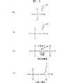
まず、本実施の形態を説明する前に、本発明者らが本発明をするのに検討した技術およびその課題等について説明する。図1(a)から(c)は、半導体集積回路装置の層間絶縁膜材料として一般的に用いられる酸化シリコン膜(SiO2等)に対して、フロロカーボン(CxFy)ガス、酸素(O2)ガスおよびアルゴン(Ar)ガス雰囲気中においてプラズマドライエッチング処理を施した場合エッチング原理を模式的に示した説明図である。
図1(a)に示すように、エッチング処理室内においてプラズマを生成すると、プラズマ中のCFラジカル等が酸化シリコン膜の表面に吸着し、CF系の堆積物が形成される。O*は酸素ラジカルを示している。この状態で、図1(b)に示すように、CFx+、Ar+またはO+等のようなエネルギーを持ったイオンが酸化シリコン膜の表面に入射すると、酸化シリコン膜の表面およびその近傍においては化学反応が生じ易いホットスポットが形成される。これにより、そのイオンのエネルギーを得てCF系の堆積物中のフッ素(F)と、酸化シリコン膜中のシリコン(Si)とが反応することにより、図1(c)に示すように、四フッ化シリコン(SiF4)が生成される。また、CF系の堆積物中の炭素(C)と酸化シリコン膜中の酸素等とが反応して一酸化炭素(CO)または二酸化炭素(CO2)等が生成される。SiF4、CO、CO2は揮発性が高いので共に排気される。このようにして酸化シリコン膜のエッチングが行われる。この場合、酸化シリコン膜のエッチングは、イオンアシストエッチングによって進行し、ケミカルエッチングによっては進行しない。
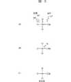
次に、図2(a)から(d)は、上記層間絶縁膜材料として、例えば有機SOG(Spin On Glass)等のような有機絶縁膜を用いた場合において、上記のような酸素を含むガス雰囲気中においてプラズマドライエッチングを施した場合のエッチング原理を模式的に示した説明図である。図2(a)は、有機絶縁膜の原子構造を模式的に示している。Siの4本の結合手のうち、3本には酸素が結合され、1本にはメチル基(CH3)が結合されている。この構造では、プラズマ中のO*等が、CH3とSiとの結合間に最も入り易い。その結果、有機絶縁膜にO*が近づくと、図2(b)に示すように、CH3とSiとの間に酸素が介在される構造となる。この状態で、更にO*が有機絶縁膜に近づくと、図2(c)に示すような準安定構造となる。この場合、構造中の酸素同士の結合間では反発する力が作用するのに対し、酸化シリコン膜中の酸素とCH3の水素とは互いに引き合う力が作用する。その結果、図2(d)に示すように、揮発性の高いCOH2が生成され、有機絶縁膜からCH3が除去される。すなわち、酸素添加ガス雰囲気中における有機絶縁膜のプラズマドライエッチング処理においては、O*が有機絶縁膜中のCH3を引き抜いてしまう結果、有機絶縁膜はポーラス化される。本発明者が行った分子軌道法による計算によれば、酸素添加ガス雰囲気中における有機絶縁膜のプラズマドライエッチング処理は、イオンアシストエッチングのみではなく、O*によるケミカルエッチングによって進行することが判明した。
ところで、O*は、CF系の堆積物中のC2F4をケミカルエッチングする。例えば図3(a)に示すように、O*がC2F4に近づくと、最終的に揮発性の高いCOF2に分解されてしまう。しかし、O*は、CF系の堆積物中のC2F5HやC2H6等をケミカルエッチングしない(イオンアシストは起こる)。例えば図3(b)に示すようにO*が、C2F5Hに近づいても酸素はフッ素と結合され化学反応が生じない。また、例えば図3(c)に示すように、O*がC2H6に近づいてもその炭素と水素との間にその酸素が介在され安定な生成物が形成される。したがって、酸素原子は、CF系の堆積物の厚いところではCF系の堆積物に邪魔されて有機絶縁膜をアタックできないが、CF系の堆積物の薄いところでは有機絶縁膜をアタックできると考えられる。
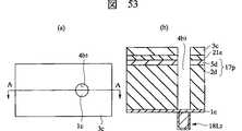
ここで、図4(a)から(e)は、例えばC4F8/O2ガスを用い、かつ、窒化シリコン膜に対するエッチング選択比を高くした状態でのプラズマドライエッチング処理によって有機絶縁膜に対してプラズマドライエッチング処理を行い有機絶縁膜に溝や孔等の凹部を形成する工程中の断面図を模式的に示している。図4(a)に示すように、絶縁膜50は、例えば窒化シリコン膜からなり、その上には、有機絶縁膜51が形成されている。有機絶縁膜51上には、フォトレジスト膜52をエッチングマスクとして、凹部53が形成されている。この凹部53の底においては、CF系の堆積物54の厚さが不均一となっている。すなわち、凹部53の底中央ではCF系の堆積物54が相対的に厚いのに対して、その底周辺ではCF系の堆積物54が相対的に薄い。このため、図4(b)に示すように、凹部53の底周辺においては、O*がCF系の堆積物54をケミカルエッチングしてしまう結果、下層の有機絶縁膜51の上面が露出される。これにより、図4(c)に示すように、凹部53の底周辺部においては、CH3が抜けてポーラス化する。これにより、その凹部53の底周辺においてO*が有機絶縁膜51をケミカルエッチングする。この状態で、図4(d)に示すように、その凹部53の底周辺部にCF+等のようなエネルギーをもったイオンが入射されると、ポーラス化された有機絶縁膜51は容易にイオンアシストエッチングされる。この結果、凹部53の底周辺に、底中央よりも深く掘り込まれた溝(以下、サブトレンチという)55が形成されてしまう。一度サブトレンチ55が形成されてしまうと、サブトレンチ55の斜面にはCF系の堆積物54が形成され難いので、図4(e)に示すように、O*のアタックを受ける結果、サブトレンチ55は大きく、深くなる。サブトレンチ55の問題は、孔や溝のアスペクト比が大きくなるほど孔や溝の底に堆積されるCF系の堆積物54の膜厚が不均一になるので顕著になる。
一方、窒化シリコン膜に対して、酸素を含むガス雰囲気中でプラズマドライエッチング処理を施すと、そのエッチングがイオンアシストのみで進行する。したがって、酸素を含むガス雰囲気中においてプラズマドライエッチング処理を施すと、有機絶縁膜は上記のようにケミカルエッチングとイオンアシストエッチングとの双方のエッチングが作用するのに対し、窒化シリコン膜はイオンアシストのみでエッチングが進行するので、エッチング選択比が高くなる。すなわち、酸素の量を増やせば有機絶縁膜と窒化シリコン膜とのエッチング選択比を高くできるが、サブトレンチは大きくなる。逆に、酸素の量を減らせばサブトレンチの発生は抑制されるが、有機絶縁膜と窒化シリコン膜とのエッチング選択比が小さくなってしまう。
このように、本発明者らの検討結果によれば、層間絶縁膜材料として有機絶縁膜を用いた場合に、そのエッチング処理に際して、酸化シリコン膜のエッチング処理時に行っている酸素を含むガス雰囲気中でのプラズマドライエッチング処理をただ単に適用すると、上記サブトレンチの問題が生じる一方、サブトレンチを抑えるべく酸素の量を減らすと、上記エッチング選択比がとれなくなる、という問題があることが見出された。
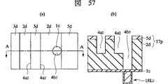
そこで、本発明者らは、プラズマエッチング処理に際し、上記酸素に代えて窒素を導入して実験した結果、サブトレンチの発生を抑制でき、かつ、エッチング選択比も確保できることを見出した。図5(a)から(c)は、有機絶縁膜を(HO)3SiCH3で表し、窒素原子を分子の近くにおいて、安定化する配置を分子軌道計算した結果を模式的に示している。この結果、図5(a)に示すように、窒素原子は、(HO)3SiCH3分子に反発され、吸着できず、反応性が低いことが分かった。ただし、窒素原子は、2eV程度のバリアを超えると、図5(b)に示すように、吸着し、図5(c)に示すように、安定化してケミカルエッチングが発生しない。したがって、有機絶縁膜は、窒素ガス添加に対しては、イオンアシストのみでエッチングが進行する。同様の分子軌道計算の結果、窒素ラジカルは、例えばC2 F5 H分子等のようなCF系の堆積物に対して、吸着できず反応性が低いことが判明した。また、C2H6やC2F4等に対しては安定エネルギーが負となり、反応にバリアがあることが判明した。したがって、窒素原子は、CF系の堆積膜をケミカルエッチングできずに、イオンアシストエッチングすると考えられる。以上のことから、窒素添加の場合は、有機絶縁膜中のCH3の引き抜き現象は生じないので、サブトレンチが発生しないと考えられる。
図6(a)から(d)は、図5で説明した窒素ガスを含むガス雰囲気中での有機絶縁膜に対するプラズマドライエッチング処理時の断面図を模式的に示している。図6(a)に示すように、窒化シリコン膜等からなる絶縁膜1上には、有機絶縁膜2が堆積され、さらに、その上にはエッチングマスクとして機能するフォトレジスト膜3がパターン形成されている。有機絶縁膜2に形成された凹部4の底には、CF系の堆積物Dが吸着されるが、この場合も、その厚さが凹部4の底面内において不均一となっている。すなわち、凹部4の底中央ではCF系の堆積物Dが相対的に厚いのに対して、その底周辺ではCF系の堆積物が相対的に薄い。しかし、図6(b)に示すように、この場合は、そのCF系の堆積物Dが薄い箇所に、N*(窒素ラジカル)が近づいても、上述のようにケミカルエッチングが生じないので、凹部4の底部外周部の有機絶縁膜2はポーラス化されないし、エッチング除去もされない。この状態で、図6(c)に示すように、CF+、Ar+またはN+等のようなエネルギーをもったイオンが凹部4の底に入射されることでイオンアシストエッチングが進行する。したがって、この場合は、そのエッチングが、凹部4の底面内においてほぼ均等に進行するので、図6(d)に示すように、凹部4の底に上記したサブトレンチが形成されない。
次に、本発明者らは、上述のようにガス種を代えて有機絶縁膜に対してプラズマドライエッチング処理を実際に行った。その実験における観測結果の模式図を図7および図8に示す。
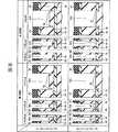
図7は、例えばC4F8/N2/Arガスを用いたプラズマドライエッチング処理を行った場合におけるアンダーエッチング時およびオーバーエッチング時の溝(凹部)4aおよび孔(凹部)4bの断面形状を模式的に示している。なお、アンダーエッチングは、溝4aおよび孔4bの底面が絶縁膜1に達せず、有機絶縁膜2の厚さ方向の途中位置で終端される程度のエッチング処理であり、オーバーエッチングは、溝4aおよび孔4bの底面が絶縁膜1に達する程度のエッチング処理である。
絶縁膜1は、例えばプラズマCVD法によって形成された窒化シリコン膜からなり、その厚さは、例えば100nm程度である。この絶縁膜1はエッチングストッパとしての機能を有している。その上の有機絶縁膜2は、例えば有機SOG膜からなり、その厚さは、例えば400nm程度である。さらに、その上の絶縁膜5は、例えばTEOS(Tetraethoxysilane)ガスを用いたプラズマCVD法によって形成された酸化シリコン膜からなり、その厚さは、例えば100nm程度である。この絶縁膜5は、主として有機絶縁膜2の機械的強度を確保するための機能を有しているものである。したがって、この絶縁膜5を設けない構造とすることもできる。溝4aは、その長さLが、例えば0.20μm、0.25μmおよび4.0μmの3種類が示されている。孔4bは、その直径が、例えば0.20μm、0.25μmおよび4.0μmの3種類が示されている。
エッチング装置としては、例えば平行平板型狭電極RIE(Reactive Ion Etching)装置を用いた。エッチング条件は、次の通りである。処理時における処理室内の圧力は、例えば20mT程度、高周波電力は、例えば1000/600W程度である。C4F8/N2/Arガスの流量比は、例えば12/200/300sccm程度である。処理時における下部電極の温度は、例えば20℃程度である。
このような窒素ガスを含むプラズマエッチングプロセスにおいては、図7に示すように、溝4aや孔4bの底部に上記したサブトレンチが発生せず、しかも、窒化シリコン膜に対する選択比が7.4程度と高い値が得られた。
一方、図8は、上記N2に代えてO2を用いた場合におけるアンダーエッチング時およびオーバーエッチング時の溝53aおよび孔53bの断面形状を模式的に示している。
絶縁膜50は、例えばTEOSガスを用いたプラズマCVD法によって形成された窒化シリコン膜からなり、その厚さは、例えば100nm程度である。その上の有機絶縁膜51は、例えば有機SOG膜からなり、その厚さは、例えば400nm程度である。さらに、その上の絶縁膜56は、例えばTEOSガスを用いたプラズマCVD法によって形成された酸化シリコン膜からなり、その厚さは、例えば100nm程度である。溝53aは、その長さLが、例えば0.20μm、0.25μmおよび4.0μmの3種類が示されている。孔53bは、その直径が、例えば0.20μm、0.25μmおよび4.0μmの3種類が示されている。
エッチング装置としては、例えば平行平板型狭電極RIE装置を用いた。エッチング条件は、次の通りである。処理時における処理室内の圧力は、例えば30mT程度、高周波電力は、例えば2200/1400W程度である。C4F8/O2/Arガスの流量比は、例えば13/15/420sccm程度である。処理時における下部電極の温度は、例えば−20℃程度である。
このような酸素ガスを含むプラズマドライエッチングプロセスにおいては、アンダーエッチングにおいて、直径が0.25μm程度およびそれ以下の小さな孔53bを除いて、サブトレンチ(異常形状)55が観測される。小さな孔53bにおいては、サブトレンチ54同士がつながってしまうため、見かけ上、サブトレンチ55が観測されない。このプロセスでは、窒化シリコン膜に対する選択比が5.0以下と低く、オーバーエッチングをかけるとサブトレンチ55が窒化シリコン膜等からなる絶縁膜50を突き抜けてしまう。すなわち、エッチングストッパとしての機能が保証されない。
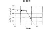
次に、図9に、上記窒素ガスを含むガス雰囲気中でのプラズマドライエッチング処理における有機絶縁膜のエッチングレートと窒化シリコン膜に対するエッチング選択比の窒素ガス流量依存性を示す。
窒素ガス流量が0(零)では、有機絶縁膜のエッチングが進行しないことから、窒素が有機絶縁膜のエッチングに必要であることがわかる。有機絶縁膜に、直径が、例えば0.25μm程度の孔を形成する際のエッチングレートと窒化シリコン膜に対するエッチング選択比は、窒素ガス流量に対して200sccm(炭素(C)/窒素(N)比が0.12)付近で極大値を持つ。図9から実用的なエッチング選択比とエッチングレートとが得られるのは、窒素ガス流量が150sccm(C/N比が0.16)から300sccm(C/N比が0.08)の場合だが、窒素ガス流量は、50sccm(C/N比が0.48)から500sccm(C/N比が0.048)でも良い。
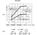
以上のようなガス種による有機絶縁膜のエッチング特性を図10に示す。CF系ガスのみによるエッチングでは、エッチングレートが遅く、エッチング選択比が低く、抜け性(エッチング除去状態の良否)は悪い。CF系ガスに酸素を添加したエッチングでは、エッチングレートおよびエッチング選択比と異常形状(特にサブトレンチ)とがトレードオフの関係にある。抜け性は良い。これに対して、本発明のCF系ガスに窒素を添加したエッチングでは、エッチングレートも400nm/min程度が得られ、サブトレンチ無しに窒化シリコン膜に対するエッチング選択比を7.4以上得ることができる。総合的に見ると、CF系ガスに窒素を添加したエッチングが、CF系ガスのみのエッチングやCF系ガスに酸素を添加したエッチングよりもエッチング特性が優れている。
次に、上記プラズマドライエッチング処理で用いた平行平板型のRIE装置6を図11に示す。このRIE装置6は、例えば2周波励起容量結合型のプラズマ源を持ち、エッチングチャンバ6aと、その内部に設置された下部電極6bと、これに電気的に接続された第1の高周波電源6cと、エッチングチャンバ6a内において下部電極6bに対向するように設置された上部電極6dと、これに電気的に接続された第2の高周波電極6eと、エッチングチャンバ6a内にガスを導入するガス導入系6fと、エッチングチャンバ6a内の圧力を一定に保つための排気系とを有している。半導体ウエハ(半導体集積回路基板)7は、下部電極6b上に配置されている。また、上記雰囲気ガスは、ガス導入系6fを通じて上部電極6dの下面側に供給され、さらにシャワープレート6gを介してエッチングチャンバ6a内に均等に供給される構造となっている。これら相対する下部電極6bと上部電極6dとの間にプラズマが形成される。ラジカル、原子、イオン等のような活性種は、下部電極6bおよび半導体ウエハ7の主面に対して垂直な電界に沿って入射し、その方向にリアクティブエッチングが進行するようになっている。ただし、エッチング装置としては、上記平行平板型狭電極RIE装置に限定されるものではなく種々変更可能であり、例えばICP(Inductively Coupled Plasma)型やECR(Electron Cyclotron Resonance)型のエッチング装置を用いることもできる。
図12は、ICP型のエッチング装置8を示している。エッチング装置8は、エッチングチャンバ8aと、その内部に設置された下部電極8bと、これに電気的に接続された第1の高周波電源8cと、エッチングチャンバ8aの上部外周に設置されたICPコイル8dと、これに電気的に接続された第2の高周波電源8eと、エッチングチャンバ8a内にガスを導入するガス導入系8fと、エッチングチャンバ8a内の圧力を一定に保つための排気系とを有している。半導体ウエハ(半導体集積回路基板)7は、下部電極8b上に配置されている。エッチングガスは、エッチングチャンバ8aの上部からエッチングチャンバ8a内に供給される。その状態で、第2の高周波電源8eからICPコイル8dに高周波電力が印加されることにより、エッチングチャンバ8a内にプラズマが形成される。また、第1の高周波電源8cは、イオネネルギーを制御するためのバイアス高周波電力を下部電極8bに供給するための電源である。
また、図13は、例えば平板アンテナ型UHF−ECR型のエッチング装置9を示している。エッチング装置9は、エッチングチャンバ9aと、その内部に設置された下部電極9bと、これに電気的に接続された第1の高周波電源9cと、エッチングチャンバ9aの上部に設置された平板状のアンテナ9dと、これに電気的に接続された第2の高周波電源9eおよびUHF電源9fと、電磁石9gと、エッチングチャンバ9a内にガスを導入するガス導入系と、エッチングチャンバ9a内の圧力を一定に保つための排気系とを有している。このアンテナ9dから放射される、例えば450MHzのUHF波と電磁石9gとによって形成される磁場によりECRを発生させ、エッチングガスをプラズマ化する。アンテナ9dの表面には、ガス導入および活性種制御のため、例えばシリコン等からなるシャワープレート9hが設置されている。アンテナ9dには、例えば13.56MHzの高周波電力を別途印加することで、シャワープレート9hに入射するイオンエネルギーを制御できる。下部電極9bにも、例えば800kHzの高周波バイアスを印加することにより、半導体ウエハ7への入射エネルギーを制御できるようになっている。また、アンテナ9dと下部電極9bとの間の距離は可変であり、プラズマ中のガスの解離を制御できるようになっている。なお、上記周波数は一例である。また、周波数の組み合わせも種々変更可能である。
以上の説明では処理ガスの種類を限定して記述したが、本発明の技術思想を用いる実施の形態においては、上記したものに限定されるものではなく種々変更可能である。
例えば上記の説明においては有機絶縁膜のエッチング処理に用いるCF系ガスとして対SiN選択比を得やすいC4F8を用いたが、これに限定されるものではなく種々変更可能であり、例えばCHF3CF4、CH2F2またはC5F8等を用いることもできる。また、その他に、CF系のガスとして、C3F6等のような飽和環状フロロカーボン、C5F9等のような非飽和環状フロロカーボン、CF4、CHF3またはCH2F2等のような非環状フロロカーボン、または、フロン対策として開発されているものにCF3I等のようなヨウ化フロロカーボン等がある。また、CF系のガスに代えて、例えばSF6を用いることもできる。
また、上記CF系/N2/ArガスのNに代えて、CF系/N2/Arガス中に、CF系ガスよりも少ない流量の酸素、すなわち、上記サブトレンチが生じないか又は生じても許容値の範囲内となる程度の酸素を添加しても良い。エッチング処理時には、エッチングと堆積との2つの要素が進行しているが、窒素のみの場合は、その堆積性が比較的高い場合がある。そこで、酸素を少量添加することで、その堆積性を抑えて抜け性(エッチング除去状態の良否)を向上させることができる。
また、上記CF系/N2/ArガスのN2に代えて、例えばNO、NO2またはNH3を用いることもできる。ただし、この場合は、ただ単にNOやNO2を導入すれば良いのではなく、上記サブトレンチの問題を考慮した酸素量の制御が必要である。
また、上記CF系/N2/Arガス中のArガスは添加しなくても良い。例えばICP型のエッチング装置を用いた場合にはプラズマの安定性が高いのでArを添加しなくても良い場合もある。また、そのArに代えてヘリウム(He)を添加することもできる。
次に、本発明の技術思想を用いて製造された半導体集積回路装置の一例を図14に示す。図14は、本発明の技術思想を、例えばCMIS(Complementary MIS)回路を有する半導体集積回路装置に適用した場合における半導体基板(半導体集積回路基板)7sの要部断面図を示している。この半導体基板7sは、上記半導体ウエハを切断して得られた平面四角形状の半導体チップを構成する基板であり、例えばp−型のシリコン単結晶からなる。半導体基板7sの主面から所定の深さに渡っては、nウエル10Nおよびpウエル10Pが形成されている。nウエル10Nには、例えばリンまたはヒ素が含有されている。また、pウエル10Pには、例えばホウ素が含有されている。また、半導体基板7sの主面側には、例えば溝型の分離部11が形成されている。この分離部11は、半導体基板7sの主面から半導体基板7sの厚さ方向に掘られた溝内に、例えば酸化シリコン膜からなる分離用の絶縁膜が埋め込まれて形成されている。
この分離部11に囲まれた活性領域には、pMISQpおよびnMISQnが形成されている。pMISQpおよびnMISQnのゲート絶縁膜12は、例えば酸化シリコン膜からなる。このゲート絶縁膜12に対して窒化処理を施すことにより、ゲート絶縁膜12と半導体基板7sとの界面に窒素を偏析させても良い。これにより、pMISQpおよびnMISQnにおけるホットキャリア効果を抑制できるので、微細化を確保したまま素子特性を向上させることができる。また、pMISQpおよびnMISQnのゲート電極13は、例えば低抵抗ポリシリコン上に、例えばコバルトシリサイドまたはタングステンシリサイド等のようなシリサイド膜を設けた、いわゆるポリサイド構造となっている。ただし、ゲート電極13は、例えば低抵抗ポリシリコンの単体膜で形成しても良いし、例えば低抵抗ポリシリコン膜上に窒化チタンや窒化タングステン等のようなバリア層を介してタングステン等のような金属膜を設けた、いわゆるポリメタル構造としても良い。ゲート長は、例えば0.14μm程度である。このゲート電極13の側面には、例えば酸化シリコン膜または窒化シリコン膜からなるサイドウォール14が形成されている。また、pMISQpのソース、ドレイン領域を構成する半導体領域15aには、例えばホウ素が含有されている。この半導体領域15aの上面には、例えばコバルトシリサイドまたはタングステンシリサイド等のようなシリサイド層15bが形成されている。また、nMISQnのソース、ドレイン領域を構成する半導体領域16aには、例えばリンまたはヒ素が含有されている。この半導体領域16aの上面には、例えばコバルトシリサイドまたはタングステンシリサイド等のようなシリサイド層16bが形成されている。なお、ゲート電極13のシリサイド層および半導体領域15a,16a上のシリサイド層15b、16bは、同工程時に形成されている。
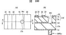
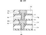
この半導体基板7sの主面上(分離部11の上面上を含む)には、層間絶縁膜17aが堆積されている。これにより、pMISQpおよびnMISQnは覆われている。この層間絶縁膜17aの上面はCMP(Chemical Mechanical Polish)法等によって平坦化されている。層間絶縁膜17aの上面には、第1層配線18L1が形成されている。第1層配線18L1は、例えばタングステンからなり、層間絶縁膜17aに穿孔された平面略円形状のコンタクトホール(凹部)19内の導体膜20を通じて上記pMISQpまたはnMISQnの半導体領域15a、16aと電気的に接続されている。導体膜20は、コンタクトホール19の側面および底面に被着されたチタン、窒化チタンまたはこれらの積層膜等からなる第1の導体膜と、その第1の導体膜が被着されたコンタクトホール19の内部に埋め込まれたタングステン等からなる第2の導体膜とを有している。
この層間絶縁膜17a上には、層間絶縁膜17bが堆積されている。この層間絶縁膜17bおよび第1層配線18L1上には絶縁膜1aが堆積されている。絶縁膜1aの上層には、層間絶縁膜17cから17k、17m、17nが層間絶縁膜17cから17k、17m、17nの各々の間にそれぞれ絶縁膜1bから1kを介在させて堆積されている。
層間絶縁膜17aから17k、17m、17nは、配線構造を構成するものであり、上記した有機絶縁膜の単体膜あるいは有機絶縁膜と他の絶縁膜との積層膜で構成されている。層間絶縁膜17aから17k、17m、17nにおける有機絶縁膜の誘電率は、例えば2.7から2.8程度である。したがって、半導体集積回路装置の配線の総合的な誘電率を下げることができるので、半導体集積回路装置の動作速度を向上させることが可能な構造となっている。この層間絶縁膜17aから17k、17m、17nで用いられている有機絶縁膜(上記有機絶縁膜2に対応)の基本的な化学構造の一例を次に示す。
また、絶縁膜1aから1kは、例えば窒化シリコン膜からなり、その誘電率は、例えば7程度である。この絶縁膜1aから1kのうち、絶縁膜1a、1b、1d、1f、1h、1jは、主としてエッチングストッパ機能を有し、絶縁膜1c,1e、1g、1i、1kは、主として銅の拡散抑制機能を有している。
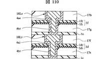
絶縁膜1aおよび層間絶縁膜17cには、スルーホール(凹部)4b1が形成されている。スルーホール4b1は、例えば平面略円形状に形成されており、第1層配線18L1の一部が露出されている。スルーホール4b1の内部には接続部(埋込配線)18PL1が形成されている。接続部18PL1は、スルーホール4b1の内側面および底面に被着された窒化チタン等からなる導体膜と、その導体膜が被着されたスルーホール4b1内に埋め込まれた銅等からなる相対的に厚い導体膜からなり、第1層配線18L1と電気的に接続されている。
絶縁膜1bおよび層間絶縁膜17dには、溝(凹部)4a1およびスルーホール(凹部)4b2が形成されている。溝4a1は、例えば平面長方形状に形成されており、その内部には第2層配線(埋込配線)18L2が形成されている。第2層配線18L2は、溝4a1の内側面および底面に被着された窒化チタン等からなる導体膜と、その導体膜が被着された溝4a1の内部に埋め込まれた銅等からなる相対的に厚い導体膜とからなり、接続部18PL1と電気的に接続されている。また、スルーホール4b2は、例えば平面略円形状に形成されており、その内部には接続部(埋込配線)18PL2が形成されている。接続部18PL2は、上記接続部18PL1と同じ構造および材料構成となっており、接続部18PL1と電気的に接続されている。
絶縁膜1c、1dおよび層間絶縁膜17e、17fには、溝(凹部)4a2,4a3およびスルーホール(凹部)4b3、4b4が形成されている。溝4a2,4a3は、例えば平面長方形状に形成されており、その内部には第3層配線(埋込配線)18L3が形成されている。ここでは、溝4a2内の第3層配線18L3がスルーホール4b3内の接続部(埋込配線)18PL3を通じて第2層配線18L2と電気的に接続されている状態が例示されている。このスルーホール4b3は、例えば平面略円形状に形成されており、溝4a2の底面から第2層配線18L2の上面に達する程度に延びている。したがって、溝4a2内の第3層配線18L3とスルーホール4b3内の接続部18PL3とは、一体的に形成されており、溝4a2おyびスルーホール4b3の内側面および底面に被着された窒化チタン等のような導体膜と、その導体膜の被着された溝4a2おyびスルーホール4b3の向上に埋め込まれた銅等からなる相対的に厚い導体膜とを有している。溝4a3内の第3層配線18L3も溝4a2内の第3層配線18L3と構造および材料構成は同じである。スルーホール4b4は、例えば平面略円形状に形成されており、層間絶縁膜17fの上面から接続部18PL2に達する程度に延びている。スルーホール4b4の内部には接続部(埋込配線)18PL4が形成されている。この接続部18PL4は、上記接続部18PL1と同じ材料構成となっており、接続部18PL2と電気的に接続されている。
絶縁膜1e、1fおよび層間絶縁膜17g、17hには、溝(凹部)4a4およびスルーホール(凹部)4b5が形成されている。溝4a4は、例えば平面長方形状に形成されており、その内部には第4層配線(埋込配線)18L4が形成されている。第4層配線18L4の構造および構成材料は第3層配線18L3と同じである。スルーホール4b5は、例えば平面略円形状に形成されており、層間絶縁膜17hの上面から第3層配線18L3や接続部18PL4に達する程度に延びている。スルーホール4b5の内部には接続部(埋込配線)18PL5が形成されている。この接続部18PL5,18PL5は、上記接続部18PL4と同じ材料構成となっており、一方は第3層配線18L3と電気的に接続され、他方は接続部18PL4と電気的に接続されている場合が例示されている。
絶縁膜1g、1hおよび層間絶縁膜17i、17jには、溝(凹部)4a5,4a6およびスルーホール(凹部)4b6、4b7が形成されている。溝4a5,4a6は、例えば平面長方形状に形成されており、その内部には第5層配線(埋込配線)18L5が形成されている。ここでは、溝4a6内の第5層配線18L5がスルーホール4b6内の接続部(埋込配線)18PL7を通じて第4層配線18L4と電気的に接続されている状態が例示されている。このスルーホール4b6は、例えば平面略円形状に形成されており、溝4a6の底面から第4層配線18L4の上面に達する程度に延びている。したがって、溝4a6内の第5層配線18L5とスルーホール4b6内の接続部18PL7とは、一体的に形成されている。この第5層配線18L5および接続部18PL7の構造および材料構成は、第3層配線18L3および接続部18PL3と同じである。溝4a5内の第5層配線18L5も溝4a6内の第5層配線18L5と構造および材料構成は同じである。スルーホール4b7は、例えば平面略円形状に形成されており、層間絶縁膜17jの上面から接続部18PL5に達する程度に延びている。スルーホール4b7の内部には接続部(埋込配線)18PL8が形成されている。この接続部18PL8は、上記接続部18PL5と同じ材料構成となっており、接続部18PL5と電気的に接続されている。
絶縁膜1i、1jおよび層間絶縁膜17k、17mには、溝(凹部)4a7,4a8およびスルーホール(凹部)4b8が形成されている。溝4a7は、例えば平面長方形状に形成されており、その内部には第6層配線(埋込配線)18L6が形成されている。ここでは、溝4a7内の第6層配線18L6がスルーホール4b8内の接続部(埋込配線)18PL9を通じて第5層配線18L5と電気的に接続されている状態が例示されている。このスルーホール4b8は、例えば平面略円形状に形成されており、溝4a7の底面から第5層配線18L5の上面に達する程度に延びている。したがって、溝4a7内の第6層配線18L6とスルーホール4b8内の接続部18PL9とは一体的に形成されており、その構造および材料構成は、上記第3層配線18L3と接続部18PL3と同じになっている。溝4a8内の第6層配線18L6も溝4a7内の第6層配線18L6と同じ構造および材料構成となっている。
絶縁膜1kおよび層間絶縁膜17nには、スルーホール(凹部)4b9が形成されている。スルーホール4b9は、例えば平面略円形状に形成されており、その底面から第6層配線18L6の一部が露出されている。スルーホール4b9の内部には接続部(埋込配線)18PL10が形成されている。接続部18PL10の構造および材料構成は、接続部18PL1等と同じである。接続部18PL10は、第6層配線18L6と電気的に接続されている。この層間絶縁膜17n上には、第7層配線18L7が形成されている。第7層配線18L7は、例えば窒化チタン、アルミニウムおよび窒化チタンが下層から順に堆積されてなり、接続部18PL10と電気的に接続されている。
なお、第2層配線18PL2は、シングルダマシン法で形成され、第3層配線18L3から18L6は、デュアルダマシン法で形成され、第1層配線18L1および第7層配線18L7は、通常の配線形成方法(導体膜の堆積およびパターニング)で形成されている。また、第1層配線18L1から第5層配線18L5の厚さは、例えば400nm程度、配線幅および最小の配線間隔は、例えば0.25μm程度である。第6層配線18L6の厚さは、例えば1200nm程度、配線幅および最小の配線間隔は、例えば0.75μm程度である。第7層配線18L7の厚さは、例えば2000nm程度、配線幅および最小の配線間隔は、例えば1.5μm程度である。接続部18PL3から18PL9の高さは、例えば500nm程度、直径は、例えば0.25μm程度である。接続部18PL10の高さは、例えば1200nm程度、直径は、例えば0.75μm程度である。
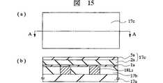
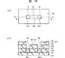
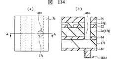
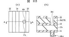
次に、本発明の技術思想を上記半導体集積回路装置の製造方法に適用した場合について図15から図36によって説明する。なお、図15から図36の各図において、(a)は図14の半導体集積回路装置の製造工程中における要部平面図、(b)は(a)のA−A線の断面図である。また、以降の半導体集積回路装置の製造方法の説明においては、説明を簡単にするため図14の一部を抜き出した図を示すものとする。
まず、本発明の技術思想をシングルダマシン法に適用した場合の一例を説明する。図15に示す上記層間絶縁膜17cは、上記絶縁膜1a上に堆積された有機絶縁膜2aと、その上に堆積された絶縁膜5aとを有している。絶縁膜1aの厚さは、例えば50nm程度である。有機絶縁膜2aは、例えば有機SOG膜によって形成され、その厚さは、例えば250nm程度である。絶縁膜5aは、例えばTEOSガスを用いたプラズマCVD法によって形成された酸化シリコン膜等からなり、その厚さは、例えば100nm程度である。この絶縁膜5aは、有機絶縁膜2aの機械的強度を確保するためのものなので、有機絶縁膜2aが機械的な強度を有している場合には、絶縁膜5aを設けなくても良い。
このような層間絶縁膜17c上に、図16に示すように、例えば厚さ120nm程度の反射防止膜21aを塗布する。続いて、その反射防止膜21a上に、フォトレジスト膜(マスキング層)3aを形成する。このフォトレジスト膜3aは、スルーホール形成用のマスクパターンであって、スルーホール形成領域が露出され、かつ、それ以外の領域が覆われるようにパターニングされている。その後、このフォトレジスト膜3aをエッチングマスクとして、そこから露出する反射防止膜21a、層間絶縁膜17cをプラズマドライエッチング処理によって順に除去する。これにより、図17に示すように、スルーホール4b1を形成する。このスルーホール4b1の底面に窒化シリコン膜等からなる絶縁膜1aが残されている。スルーホール4b1の直径は、例えば0.25μm程度である。
上記反射防止膜21aのエッチング条件は次の通りである。すなわち、処理ガスは、例えばCHF3/CF4/Arを用い、その流量比は、例えば10/90/950sccm程度である。処理室内の圧力は、例えば750mTorr程度、高周波電力は、例えば900W程度、下部電極温度は、例えば10℃程度である。エッチング装置としては、例えば平行平板型狭電極RIE装置を用いた。
また、上記層間絶縁膜17cのエッチング処理においては、上記本発明の技術思想を用いている。したがって、スルーホール4b1の底にサブトレンチを生じさせることなく、しかも窒化シリコン膜に対するエッチング選択比を高くした状態でエッチング処理が可能である。このエッチング条件は、次の通りである。すなわち、処理ガスは、例えばC4F8/N2/Arを用い、その流量比は、例えば12/200/300sccm程度である。処理室内の圧力は、例えば20mTorr程度、高周波電力は、例えば1000/600W程度、下部電極温度は、例えば20℃程度である。エッチング装置としては、例えば平行平板型狭電極RIE装置を用いた。
次いで、フォトレジスト膜3aおよび反射防止膜21aをアッシング処理によって図18に示すように除去した後、スルーホール4b1の底面から露出する絶縁膜1aをプラズマドライエッチング処理によって図19に示すように除去する。このエッチング処理では、窒化シリコン膜を選択的にエッチング除去する。これにより、スルーホール4b1の底面から第1層配線18L1の上面が露出される。この際のエッチング条件は、次の通りである。すなわち、処理ガスは、例えばCHF3/O2/Arを用い、その流量比は、例えば20/20/400sccm程度である。処理室内の圧力は、例えば50mTorr程度、高周波電力は、例えば1000/200W程度、下部電極温度は、例えば0℃程度である。エッチング装置としては、例えば平行平板型狭電極RIE装置を用いた。
次いで、例えば窒化チタン(TiN)、タンタル(Ta)または窒化タンタル(TaN)等からなるバリア導体膜を、層間絶縁膜17c上およびスルーホール4b1内にスパッタリング法によって堆積する。このバリア導体膜は、銅原子の拡散を抑制する機能や配線と層間絶縁膜との密着性を向上させる機能を有している。続いて、そのバリア導体膜上に、例えば銅からなる薄いシード(Seed)導体膜をスパッタリング法によって堆積した後、そのシード導体膜上に、例えば銅からなる主導体膜をメッキ法によって堆積する。その後、その主導体膜、シード導体膜およびバリア導体膜の不要な部分をCMP法等によって研磨して除去することにより、図20に示すように、スルーホール4b1内に接続部18PL1を形成する。
次いで、図21に示すように、層間絶縁膜17cおよび接続部18PL1の上面上に、上記絶縁膜1bをプラズマCVD法等によって堆積した後、その上に、層間絶縁膜17dを堆積する。層間絶縁膜17dは、有機絶縁膜2bとその上に堆積された絶縁膜5bとからなる。有機絶縁膜2bおよび絶縁膜5bの構造(形成方法、材料、厚さおよび機能等)は、それぞれ上記有機絶縁膜2aおよび絶縁膜5aの構造(形成方法、材料、厚さおよび機能等)と同じである。
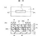
続いて、層間絶縁膜17d上に、図22に示すように、例えば上記反射防止膜21aと同じ厚さの反射防止膜21bを塗布する。その後、その反射防止膜21b上に、フォトレジスト膜3bを形成する。このフォトレジスト膜(マスキング層)3bは、配線溝形成用のマスクパターンであって、配線形成領域が露出され、かつ、それ以外の領域が覆われるようにパターニングされている。その後、このフォトレジスト膜3bをエッチングマスクとして、そこから露出する反射防止膜21bおよび層間絶縁膜17dをプラズマドライエッチング処理によって順に除去することにより、図23に示すように、溝4a1を形成する。溝4a1の底面には窒化シリコン膜からなる絶縁膜1bが残されている。
上記反射防止膜21bのエッチング条件は、上記反射防止膜21aのエッチング条件と同じである。また、上記層間絶縁膜17dのエッチング処理においては、上記本発明の技術思想を用いている。したがって、溝4a1の底にサブトレンチを生じさせることなく、しかも窒化シリコン膜に対するエッチング選択比を高くした状態でエッチング処理が可能である。この層間絶縁膜17dのエッチング条件は、上記層間絶縁膜17cのエッチング条件と同じである。
次いで、フォトレジスト膜3bおよび反射防止膜21bをアッシング処理によって図24に示すように除去した後、溝4a1の底面から露出する絶縁膜1bをプラズマドライエッチング処理によって図25に示すように除去する。これにより、溝4a1の底面から接続部18PL1の上面が露出される。この際のエッチング条件は、例えば処理ガスのCHF3/O2/Arの流量比が20/20/200sccm程度である以外は、上記絶縁膜1aのエッチング条件と同じである。続いて、例えば窒化チタン(TiN)からなるバリア導体膜を、層間絶縁膜17d上および溝4a1内にスパッタリング法によって堆積する。このバリア導体膜は、銅原子の拡散を抑制する機能および層間絶縁膜と配線との密着性を向上させる機能を有している。続いて、そのバリア導体膜上に、例えば銅からなる薄いシード(Seed)導体膜をスパッタリング法によって堆積した後、そのシード導体膜上に、例えば銅からなる主導体膜をメッキ法によって堆積する。その後、その主導体膜、シード導体膜およびバリア導体膜の不要な部分をCMP法等によって研磨して除去することにより、図26に示すように、溝4a1内に第2層配線18L2を形成する。
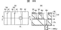
次に、本発明の技術思想をデュアルダマシン法に適用した場合の一例を説明する。なお、デュアルダマシン法の説明においては、図14の第2、第3層配線部分を一例として抜き出してその形成方法を説明するが、第4から第6層配線を形成する場合も同様の形成方法で対応できる。層間絶縁膜17gから17k、17m、17nの構造も層間絶縁膜17c、17d、17e、17fで代表されるものとする。
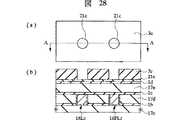
図27に示す上記絶縁膜1cは、銅の拡散を抑制する機能を有しており、その厚さは、例えば50nm程度である。その絶縁膜1c上には、層間絶縁膜17eが形成されている。この層間絶縁膜17eは、例えば上記有機絶縁膜2aと同じ材料および形成方法で形成されてなり、その厚さは、例えば400nm程度である。層間絶縁膜17e上には、上記絶縁膜1dが堆積されている。絶縁膜1dは主としてエッチングストッパとして機能し、その厚さは、例えば100nm程度である。
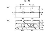
このような層間絶縁膜17e上に、図28に示すように、上記反射防止膜21a等と同じ厚さの反射防止膜21cを塗布した後、その反射防止膜21c上に、フォトレジスト膜(マスキング層)3cを形成する。このフォトレジスト膜3cは、スルーホール形成用のマスクパターンであって、スルーホール形成領域が露出され、かつ、それ以外の領域が覆われるようにパターニングされている。その後、このフォトレジスト膜3cをエッチングマスクとして、そこから露出する反射防止膜21c、絶縁膜1dをプラズマドライエッチング処理によって順に除去することにより、図29に示すように、絶縁膜1dにスルーホール4b3を形成する。このスルーホール4b3の底面からは層間絶縁膜17eが露出されている。スルーホール4b3の直径は、例えば0.25μm程度である。この残された絶縁膜1dは後述するようにエッチングマスクとして機能する。この反射防止膜21cのエッチング条件は、上記反射防止膜21aのエッチング条件と同じである。また、絶縁膜1dのエッチング条件は、例えば処理ガスのCHF3/O2/Arの流量比が20/20/200sccm程度である以外は、上記絶縁膜1aのエッチング条件と同じである。
次いで、フォトレジスト膜3cおよび反射防止膜21cをアッシング処理によって図30に示すように除去した後、図31に示すように、絶縁膜1dおよびスルーホール4b3から露出する層間絶縁膜17e上に、有機絶縁膜2cおよび絶縁膜5cを下層から順に堆積して層間絶縁膜17fを形成する。有機絶縁膜2cおよび絶縁膜5cの構造(形成方法、材料、厚さおよび機能等)は、それぞれ上記有機絶縁膜2aおよび絶縁膜5aの構造(形成方法、材料、厚さおよび機能等)と同じである。
続いて、層間絶縁膜17f上に、図32に示すように、反射防止膜21dを塗布する。反射防止膜21dの厚さは、上記反射防止膜21aと同じである。その後、その反射防止膜21d上に、フォトレジスト膜(マスキング層)3dを形成する。このフォトレジスト膜3dは、配線溝形成用のマスクパターンであって、配線形成領域が露出され、かつ、それ以外の領域が覆われるようにパターニングされている。その後、このフォトレジスト膜3dをエッチングマスクとして、そこから露出する反射防止膜21dおよび層間絶縁膜17f,17eをプラズマドライエッチング処理によって順に除去する。これにより、図33に示すように、層間絶縁膜17fに溝4a2を形成し、かつ、層間絶縁膜17eにスルーホール4b3を形成する。すなわち、1エッチング工程で溝4a2およびスルーホール4b3の両方を形成することができる。この溝4a2およびスルーホール4b3の底面には、それぞれ窒化シリコン膜からなる絶縁膜1d、1cが残されている。上記反射防止膜21dのエッチング条件は、上記反射防止膜21aのエッチング条件と同じである。また、層間絶縁膜17f,17eのエッチング処理では、絶縁膜1c、1dをエッチングストッパとして機能させる。そのエッチング条件は、上記層間絶縁膜17cのエッチング条件と同じである。
次いで、フォトレジスト膜3dおよび反射防止膜21dをアッシング処理によって図34に示すように除去した後、溝4a2およびスルーホール4b3の底面から露出する絶縁膜1d、1cをプラズマドライエッチング処理によって図35に示すように除去する。このエッチング処理では、窒化シリコン膜を選択的にエッチング除去する。これにより、溝4a2の底面から層間絶縁膜17eの上面が露出され、スルーホール4b3の底面から第2層配線18L2および接続部18PL2の上面が露出される。この際のエッチング条件は、上記絶縁膜1aのエッチング条件と同じである。
続いて、例えば銅の拡散抑制機能および絶縁膜との密着性向上機能を有する窒化チタン(TiN)、タンタル(Ta)または窒化タンタル(TaN)等からなるバリア導体膜を、層間絶縁膜17f上、溝4a2およびスルーホール4b3内にスパッタリング法によって堆積した後、そのバリア導体膜上に、例えば銅からなる薄いシード(Seed)導体膜をスパッタリング法によって堆積し、さらに、その上に、例えば銅からなる主導体膜をメッキ法によって堆積する。その後、その主導体膜、シード導体膜およびバリア導体膜の不要な部分をCMP法等によって研磨して除去することにより、図36に示すように、溝4a2内に第3層配線18L3を形成し、同時に、スルーホール4b3内に、その第3層配線18L3と一体的に構成される接続部18PL3を形成する。この第3層配線18L3は、スルーホール4b3内の接続部18PL3を通じて第2層配線18L2および接続部18PL2と電気的に接続されている。すなわち、第3層配線18L3は、第2層配線18L2と接続部18PL2とを電気的に接続している。図14に示した半導体集積回路装置においては、上述の配線形成方法を第6層配線18L6まで繰り返すことにより、その配線層を形成する。なお、第7層配線18L7は、層間絶縁膜17n上に配線形成用の導体膜を堆積した後、その導体膜を通常のフォトリソグラフィ技術およびドライエッチング技術によってパターニングすることで形成する。
このような本実施の形態1によれば、以下の効果を得ることが可能となる。
(1).有機絶縁膜2,2aから2cに溝や孔等のような凹部4を形成する際に、その凹部4の底面外周にサブトレンチ55が形成されてしまうのを抑制することが可能となる。
(2).上記(1)により、半導体集積回路装置を構成する配線層における不良の発生率を低減できる。したがって、半導体集積回路装置の信頼性および歩留まりを向上させることが可能となる。
(3).上記(1)により、有機絶縁膜2,2aから2cにアスペクト比が高い溝や孔等のような凹部4を形成することが可能となる。
(4).上記(3)により、半導体集積回路装置を構成する配線の微細化が可能となり、半導体集積回路装置の高集積化が可能となる。
(5).有機絶縁膜2,2aから2cに溝や孔等の凹部4を形成する際に、窒化シリコン膜からなる絶縁膜1,1aから1kに対するエッチング選択比を高くできる。したがって、凹部4の形成時に絶縁膜1,1aから1kの突き抜けの不具合を抑制することが可能となる。
(6).上記(5)により、絶縁膜1,1aから1kを薄くすることができるので、半導体集積回路装置の配線の総合的な誘電率を下げることができる。したがって、半導体集積回路装置の動作速度を向上させることが可能となる。
(実施の形態2)
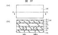
本実施の形態2は、前記実施の形態1の変形例を説明するものであって、本発明の技術思想を前記実施の形態1で説明したデュアルダマシン法とは別のデュアルダマシン法に適用した場合について説明するものである。本実施の形態2の半導体集積回路装置の製造方法を図37から図42により説明する。なお、図37から図42の各図において、(a)は図14の半導体集積回路装置の製造工程中における要部平面図、(b)は(a)のA−A線の断面図である。
まず、図27に示した絶縁膜1d上に、図37に示すように、層間絶縁膜17fを形成する。本実施の形態2においては、絶縁膜1dの材料としては前記実施の形態1と同様に窒化シリコン膜を用いているが、これに代えて、例えばTEOSガスを用いたプラズマCVD法で形成された厚さ100nm程度の酸化シリコン膜としても良い。この層間絶縁膜17fは、上記したように有機絶縁膜2c上に、絶縁膜5cが堆積されてなる。
続いて、図38に示すように、層間絶縁膜17f上に、上記反射防止膜21a等と同じ厚さの反射防止膜21eを塗布する。その後、その反射防止膜21e上に、上記フォトレジスト膜(マスキング層)3cを形成した後、このフォトレジスト膜3cをエッチングマスクとして、そこから露出する反射防止膜21e、層間絶縁膜17fをプラズマドライエッチング処理によって順に除去する。これにより、図39に示すように、層間絶縁膜17f、絶縁膜1d、層間絶縁膜17eにスルーホール4b3を形成する。このスルーホール4b3の底面からは絶縁膜1cが露出されている。スルーホール4b3の直径は、例えば0.25μm程度である。この反射防止膜21eのエッチング条件は、上記反射防止膜21aのエッチング条件と同じである。また、層間絶縁膜17f、絶縁膜1dおよび層間絶縁膜17eのエッチング処理は、例えば3段階に分けてエッチング処理を行う。すなわち、第1のエッチング処理では、酸化シリコン膜の方が窒化シリコン膜よりもエッチング除去され易い条件でエッチング処理することで絶縁膜1dをエッチングストッパとして層間絶縁膜17fをエッチング除去する。続いて、第2のエッチング処理では、窒化シリコン膜の方が酸化シリコン膜よりもエッチング除去され易い条件でエッチング処理することで絶縁膜1dをエッチング除去する。その後、第3のエッチング処理では、上記第1のエッチング処理と同様の条件で絶縁膜1cをエッチングストッパとして層間絶縁膜17eをエッチング除去する。層間絶縁膜17e、17fのエッチング処理では、本発明の技術思想を適用する。そのエッチング条件は、上記層間絶縁膜17cのエッチング条件と同じである。窒化シリコン膜等からなる絶縁膜1dのエッチング条件は、上記絶縁膜1aから1dのエッチング条件と同じである。
次いで、フォトレジスト膜3cおよび反射防止膜21eをアッシング処理によって図40に示すように除去した後、図41に示すように、層間絶縁膜17f上およびスルーホール4b3内に反射防止膜21fを塗布する。反射防止膜21fの厚さは、スルーホール4b3を埋め込むことから上記反射防止膜21aよりも厚く、例えば240nm程度である。続いて、その反射防止膜21f上に、上記フォトレジスト膜3dを形成した後、このフォトレジスト膜3dをエッチングマスクとして、そこから露出する反射防止膜21fおよび層間絶縁膜17fをプラズマドライエッチング処理によって順に除去する。これにより、図42に示すように、層間絶縁膜17fに溝4a2を形成する。なお、このエッチング処理後においては、スルーホール4b3の底部に反射防止膜21fが残されている。また、溝4a2の底面には、窒化シリコン膜からなる絶縁膜1dが残されている。
上記反射防止膜21fのエッチング条件は、次の通りである。すなわち、処理ガスは、例えばN2/O2を用い、その流量比は、例えば35/50sccm程度である。処理室内の圧力は、例えば10mTorr程度、高周波電力は、例えば500/140W程度、下部電極温度は、例えば−20℃程度である。エッチング装置としては、例えば平行平板型狭電極RIE装置を用いた。また、層間絶縁膜17fのエッチング処理は、本発明の技術思想を用いており、絶縁膜1dをエッチングストッパとして機能させる。そのエッチング条件は、上記層間絶縁膜17cのエッチング条件と同じである。
次いで、フォトレジスト膜3dおよび反射防止膜21fをアッシング処理によって除去し、前記実施の形態1で用いた図34と同じ構造を得る。これ以降の製造工程は、前記実施の形態1の図35および図36で説明した工程と同じなので説明を省略する。
このような本実施の形態2においては、前記実施の形態1で得られた効果と同様の効果を得ることが可能となる。特に、アスペクト比の高いスルーホール4b3をその断面形状に不具合を生じさせることなく、窒化シリコン膜に対する高いエッチング選択比を確保したまま形成することができる。
(実施の形態3)
本実施の形態3は、前記実施の形態1、2の変形例を説明するものであって、本発明の技術思想を前記実施の形態1、2で説明したデュアルダマシン法とは別のデュアルダマシン法に適用した場合について説明するものである。本実施の形態3の半導体集積回路装置の製造方法を図43から図50により説明する。なお、図43から図50の各図において、(a)は図14の半導体集積回路装置の製造工程中における要部平面図、(b)は(a)のA−A線の断面図である。
まず、図37に示した層間絶縁膜17f上に、図43に示すように、例えば窒化シリコン膜からなる絶縁膜22を形成する。この絶縁膜22は、溝や孔形成時のエッチングマスク用の部材であり、その厚さは、例えば150nm程度である。ただし、絶縁膜22は、窒化シリコン膜に限定されるものではなく種々変更可能であり、例えば窒化チタン、タンタル、窒化タンタル、ポリシリコンまたはこれら絶縁膜22として使用できる膜のうち、少なくとも1種類を含む膜を用いても良い。
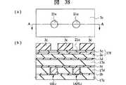
続いて、図44に示すように、絶縁膜22上に、反射防止膜21eを塗布する。その後、その反射防止膜21e上に、上記フォトレジスト膜(マスキング層)3dを形成した後、このフォトレジスト膜3dをエッチングマスクとして、そこから露出する反射防止膜21eおよび絶縁膜22をプラズマドライエッチング処理によって順に除去する。これにより、絶縁膜22に層間絶縁膜17fの上面が露出されるような開口部23を形成する。上記反射防止膜21eのエッチング条件は、上記反射防止膜21aのエッチング条件と同じである。また、絶縁膜22のエッチング条件は、上記絶縁膜1dのエッチング条件と同じである。
次いで、フォトレジスト膜3dをアッシング処理によって図46に示すように除去した後、図47に示すように、絶縁膜22上および開口部23内に、上記反射防止膜21aと同じ厚さの反射防止膜21gを塗布する。続いて、その反射防止膜21g上に、上記フォトレジスト膜3cを形成した後、このフォトレジスト膜3cをエッチングマスクとして、そこから露出する反射防止膜21g、層間絶縁膜17f、絶縁膜1dおよび層間絶縁膜17eをプラズマドライエッチング処理によって順に除去する。これにより、図48に示すように、層間絶縁膜17f、絶縁膜1dおよび層間絶縁膜17eにスルーホール4b3を形成する。スルーホール4b3の底面には層間絶縁膜17eが残されている。
上記反射防止膜21gのエッチング条件は、反射防止膜21aのエッチング条件と同じである。また、層間絶縁膜17f、絶縁膜1dおよび層間絶縁膜17eのエッチング条件は、次の通りである。すなわち、処理ガスは、例えばCHF3/O2/Arを用い、その流量比は、例えば50/10/500sccm程度である。処理室内の圧力は、例えば50mTorr程度、高周波電力は、例えば2200/1400W程度、下部電極温度は、例えば−20℃程度である。エッチング装置としては、例えば平行平板型狭電極RIE装置を用いた。エッチング終点はエッチング時間の設定によって行っている。
次いで、フォトレジスト膜3cおよび反射防止膜21fをアッシング処理によって図49に示すように除去した後、残された絶縁膜22をエッチングマスクとし、かつ、絶縁膜1c、1dをエッチングストッパとして、開口部23およびスルーホール4b3の底面から露出する層間絶縁膜17eをプラズマドライエッチング処理によって図50に示すように除去する。これにより、溝4a2およびスルーホール4b3を形成する。この溝4a2の底面からは、絶縁膜1dの上面が露出され、スルーホール4b3の底面からは、絶縁膜1cの上面が露出される。この際のエッチング処理は、本発明の技術思想を用いており、その条件は、上記層間絶縁膜17cのエッチング条件と同じである。
その後、絶縁膜1c、1d、22をプラズマドライエッチング処理によって除去する。このエッチング処理に際しては、窒化シリコン膜を選択的に除去する。このエッチング条件は、上記絶縁膜1aのエッチング条件と同じである。このようにして、前記実施の形態1で用いた図34と同じ構造を得る。これ以降の製造工程は、前記実施の形態1の図35および図36で説明した工程と同じなので説明を省略する。
このような本実施の形態3においては、前記実施の形態1で得られた効果と同様の効果を得ることが可能となる。
(実施の形態4)
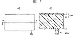
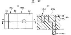
本実施の形態4は、前記実施の形態1の変形例を説明するものであって、層間絶縁膜の中間層に、窒化シリコン膜からなりエッチングストッパとして機能する絶縁膜を設けないで埋込配線を形成するデュアルダマシン法に本発明の技術思想を適用した場合について説明するものである。本実施の形態4の半導体集積回路装置の製造方法を図51から図59により説明する。なお、図51から図59の各図において、(a)は半導体集積回路装置の製造工程中における要部平面図、(b)は(a)のA−A線の断面図である。
図51に示すように、上記絶縁膜1c上には、層間絶縁膜17pが堆積されている。層間絶縁膜17pは、有機絶縁膜2dおよび絶縁膜5dが下層から順に堆積されてなる。有機絶縁膜2dは、上記有機絶縁膜2aから2cと同じ材料および形成方法からなるが、その厚さが、上述したものよりも厚く、例えば650から800nm程度である。また、絶縁膜5dは、上記絶縁膜5aから5cと同じ材料、同じ厚さ、形成方法および機能を有している。
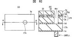
まず、図51に示した層間絶縁膜17p上に、図52に示すように、上記反射防止膜21eを塗布した後、上記フォトレジスト膜(マスキング層)3cを形成する。続いて、このフォトレジスト膜3cをエッチングマスクとして、そこから露出する反射防止膜21e、層間絶縁膜17pをプラズマドライエッチング処理によって除去する。これにより、図53に示すように、層間絶縁膜17pにスルーホール4b3を形成する。このスルーホール4b3の底面からは絶縁膜1cが露出されている。この反射防止膜21eのエッチング条件は、上記反射防止膜21aのエッチング条件と同じである。また、層間絶縁膜17pのエッチング処理は、本発明の技術思想を用い、絶縁膜1cをエッチングストッパとして行っており、そのエッチング条件は、上記層間絶縁膜17cのエッチング条件と同じである。
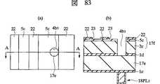
次いで、フォトレジスト膜3cをアッシング処理によって図54に示すように除去した後、図55に示すように、層間絶縁膜17p上およびスルーホール4b3内に反射防止膜21fを塗布する。続いて、その反射防止膜21f上に、上記フォトレジスト膜3dを形成した後、このフォトレジスト膜3dをエッチングマスクとして、そこから露出する反射防止膜21fおよび層間絶縁膜17pをプラズマドライエッチング処理によって除去する。これにより、図56に示すように、層間絶縁膜17pに溝4a2を形成する。
上記反射防止膜21fのエッチング条件は、次の通りである。すなわち、処理ガスは、例えばN2/O2を用い、その流量比は、例えば35/50sccm程度である。処理室内の圧力は、例えば10mTorr程度、高周波電力は、例えば500/140W程度、下部電極温度は、例えば−20℃程度である。エッチング装置としては、例えば平行平板型狭電極RIE装置を用いた。このエッチング処理後においては、溝4a2およびスルーホール4b3内反射防止膜21fが残されている。
また、層間絶縁膜17pのエッチング条件は、上記層間絶縁膜17cのエッチング条件と同じである。ただし、本実施の形態4においては、層間絶縁膜17pの厚さ方向の途中位置に窒化シリコン等からなるエッチングストッパ層を設けてないので、この層間絶縁膜17pのエッチング処理に際しては、そのエッチング終点をエッチング時間によって決めている。すなわち、溝4a2の深さをエッチング時間によって決めている。
次いで、フォトレジスト膜3dおよび反射防止膜21fをアッシング処理によって図57に示すように除去する。続いて、スルーホール4b3の底部の絶縁膜1cを図58に示すように前記実施の形態1から3で説明したように選択的にエッチング除去することにより、スルーホール4b3の底面から第2層配線18L2の一部を露出させる。その後、前記実施の形態1から3と同様にスルーホール4b3および溝4a2内に導体膜を埋め込むことにより、図59に示すように第3層配線18L3を形成する。
本実施の形態4においては、前記実施の形態1から3で得られた効果の他に、以下の効果を得ることが可能となる。すなわち、層間絶縁膜17pの中間層に窒化シリコン膜からなる絶縁膜(前記絶縁膜1d等)を設けないことにより、半導体集積回路装置の配線の総合的な誘電率を下げることができるので、半導体集積回路装置の動作速度をさらに向上させることが可能となる。
(実施の形態5)
本実施の形態5は、本発明の他の技術思想を説明するものであって、有機絶縁膜に対して、フロロカーボンガスおよび酸素ガスを含むガス雰囲気中においてプラズマエッチング処理を施すことにより、その有機絶縁膜に配線形成用の溝や孔等のような凹部を形成する際に、そのエッチング処理中にエッチング条件を変えて複数段階に分けて処理を行うものである。
本発明者らは、上記有機絶縁膜に溝や孔等のような凹部を形成するためのエッチング処理に際し、処理ガス中の酸素の量と上記サブトレンチおよび窒化シリコン膜に対するエッチング選択比との関係について検討した。図60は、その検討結果を示すものである。なお、下記のいずれのエッチング処理もエッチング装置は上記実施の形態1で説明した平行平板型のRIE装置を用いた。また、いずれの場合も高周波電力は、例えば3から0.2kW程度である。また、いずれの場合も、被処理用の半導体集積回路基板として、例えば直径8インチ程度の半導体ウエハを用いた。
図60の左側は、上記凹部4の形状を優先してエッチング条件を設定した場合である(形状優先条件)。処理ガスとしては、例えばC4F8/O2/Arガスを用い、その流量比は、例えば100から5/90から0/1000から0sccm程度である。ただし、ここでは、C4F8流量>O2流量とする。この場合、凹部4の形状は良好であるが、エッチング選択比は2以下と低くなる。
一方、図60の右側は、上部窒化シリコン膜に対するエッチング選択比を優先としてエッチング条件を設定した場合である(高選択比条件)。処理ガスとしては、例えばC4F8/O2/Arガスを用い、その流量比は、例えば100から5/90から0/1000から0sccm程度である。ただし、ここでは、C4F8流量≦O2流量とする。この場合、凹部4の底にサブトレンチ55が形成されているが、エッチング選択比は5まで確保できる。
このようにいずれか一方のエッチング条件のみで有機絶縁膜2に凹部4を形成しようとすると問題が生じる。そこで、本発明の技術思想においては、上記有機絶縁膜に上記溝や孔等のような凹部を形成する際に、1回のエッチング処理で形成するのではなく、有機絶縁膜の途中の深さまでは上記形状優先条件でエッチング処理を行い、その後、残りの有機絶縁膜を上記高選択比条件でエッチング除去するものである。
本発明の技術思想を上記シングルダマシン法に適用した場合を図61によって説明する。まず、図61(a)に示すように、絶縁膜5上にフォトレジスト膜3を形成した後、このフォトレジスト膜3をエッチングマスクとして1回目のエッチング処理を施すことにより絶縁膜5および有機絶縁膜2に溝または孔等のような凹部4を形成する。この1回目のエッチング処理においては、エッチング条件を上記した形状優先条件(例えばC4F8流量>O2流量)とし、窒化シリコン膜等からなる絶縁膜1の直上までエッチング処理を行う。すなわち、この処理後においては、凹部4の底面には、有機絶縁膜2が残され、絶縁膜1が露出されない。この凹部4の底部に残されている有機絶縁膜2の厚さは、エッチング処理前の元の有機絶縁膜2の厚さの30%以下、あるいは20%以下、好ましくは15%以下である。
続いて、図61(b)に示すように、フォトレジスト膜3をそのままエッチングマスクとして2回目のエッチング処理を施すことによりフォトレジスト膜3から露出された残りの有機絶縁膜2を除去して凹部4を完成させる。この2回目のエッチング処理においては、エッチング条件を上記した高選択比条件(例えばC4F8流量≦O2流量)とする。このため、窒化シリコン膜に対するエッチング選択比を高くした状態でエッチング処理を行うことが可能である。また、凹部4の底部に小さなサブトレンチ55が発生するが、これは許容の範囲であって絶縁膜1の上部の一部が削れる程度のものである。この処理後においては、凹部4の底面から絶縁膜1が露出される。
次に、本発明の技術思想を上記デュアルダマシン法に適用した場合を図62によって説明する。なお、図62(a)の絶縁膜1A,1Bは、例えば窒化シリコン膜からなる上記絶縁膜1に対応し、有機絶縁膜2A,2Bは、上記した有機絶縁膜2に対応している。絶縁膜1Bは、有機絶縁膜2A,2Bの間に形成され、孔形成用の開口部23が形成されている。
まず、図62(a)に示すように、絶縁膜5上にフォトレジスト膜3を形成した後、このフォトレジスト膜3をエッチングマスクとして1回目のエッチング処理を施すことにより、図62(b)に示すように、絶縁膜5および有機絶縁膜2Bに溝または孔等のような凹部4Aを形成する。この1回目のエッチング処理においては、エッチング条件を上記した形状優先条件(例えばC4F8流量>O2流量)とし、絶縁膜1Bの直上までエッチング処理を行う。すなわち、この処理後においては、凹部4Aの底面には、有機絶縁膜2Bが残され、その底面から絶縁膜1Bが露出されない。この凹部4Aの底部に残されている有機絶縁膜2Bの厚さは、エッチング処理前の元の有機絶縁膜2Bの厚さの30%以下、あるいは20%以下、好ましくは15%以下である。
続いて、図62(c)に示すように、フォトレジスト膜3をそのままエッチングマスクとして2回目のエッチング処理を施すことによりフォトレジスト膜3から露出された残りの有機絶縁膜2Bを除去する。そして、そのままエッチング処理を進めることにより、絶縁膜1Bをエッチングマスクとして絶縁膜1Bから露出する有機絶縁膜2Aをも除去する。これにより、凹部4A、4Bを完成させる。この2回目のエッチング処理においては、エッチング条件を上記した高選択比条件(例えばC4F8流量≦O2流量)とする。このため、窒化シリコン膜に対するエッチング選択比を高くした状態でエッチング処理を行うことが可能である。また、凹部4Aの底部外周に上記と同様の小さなサブトレンチ55が発生するが許容の範囲である。この処理後においては、凹部4Bの底面から絶縁膜1Aが露出される。
次に、このような本発明の技術思想を半導体集積回路装置の製造方法に適用した場合を図63から図70によって説明する。なお、図63から図70の各図において、(a)は図14の半導体集積回路装置の製造工程中における要部平面図、(b)は(a)のA−A線の断面図である。
本発明の技術思想をシングルダマシン法に適用した場合について説明する。まず、図63に示すように、前記実施の形態1と同様に、フォトレジスト膜3aをエッチングマスクとして、そこから露出する反射防止膜21aをプラズマドライエッチング処理によって除去して絶縁膜5aを露出させる。なお、ここでの有機絶縁膜2aの厚さは、例えば400nm程度である。また、フォトレジスト膜3aの厚さは、例えば0.78μm程度である。
続いて、図64に示すように、フォトレジスト膜3aをエッチングマスクとして、そこから露出する絶縁膜5aおよび有機絶縁膜2aを、例えばC4F8/O2/Arガスを用いたプラズマドライエッチング処理によって除去することによりスルーホール4b1を形成する。ただし、このエッチング処理では、エッチング条件を上記形状優先条件とし、有機絶縁膜2aの厚さ方向の途中の位置(絶縁膜1aの直上)でエッチング処理を終了する。したがって、この処理後のスルーホール4b1の底面には、サブトレンチは形成されない。また、スルーホール4b1の底面からは有機絶縁膜2aが露出され、絶縁膜1aは露出されない。この際の詳細なエッチング条件は、次の通りである。すなわち、C4F8/O2/Arガスの流量比は、例えば35/20/400sccm程度である。処理室内の圧力は、例えば25mTorr程度、高周波電力は、例えば500/200W程度、下部電極温度は、例えば−20℃程度である。エッチング装置としては、例えば平行平板型狭電極RIE装置を用いた。
その後、スルーホール4b1の底部の有機絶縁膜2aを、図65に示すように、例えばC4F8/O2/Arガスを用いたプラズマドライエッチング処理によって除去する。ただし、このエッチング処理では、エッチング条件を上記高選択比条件とし、絶縁膜1aをエッチングストッパとして機能させ、絶縁膜1aの上面が露出されるまでエッチング処理を行う。この際のエッチング条件は、次の通りである。すなわち、C4F8/O2/Arガスの流量比は、例えば13/15/420sccm程度である。処理室内の圧力は、例えば30mTorr程度、高周波電力は、例えば2200/1400程度、下部電極温度は、例えば−20℃程度である。エッチング装置としては、例えば平行平板型狭電極RIE装置を用いた。
次いで、前記実施の形態1と同様に、フォトレジスト膜3aおよび反射防止膜21aをアッシング処理によって除去した後、スルーホール4b1の底面から露出する絶縁膜1aを、例えばCHF3/O2を用いたプラズマドライエッチング処理によって図66に示すように除去することにより、第1層配線18L1の上面の一部を露出させ、スルーホール4b1を完成させる。このエッチング処理では、窒化シリコン膜を選択的にエッチング除去する。この際のエッチング条件は、次の通りである。すなわち、CHF3/O2の流量比は、例えば20/20sccm程度である。処理室内の圧力は、例えば50mTorr程度、高周波電力は、例えば1000/200W程度、下部電極温度は、例えば−10℃程度である。エッチング装置としては、例えば平行平板型狭電極RIE装置を用いた。その後、前記実施の形態1と同様に、スルーホール4b1内に、導体膜を埋め込み、接続部18PL1を形成する。
次に、本発明の技術思想をデュアルダマシン法に適用した場合について説明する。図67は、前記実施の形態1の図27から図32で説明した工程を経た後の本実施の形態5の半導体集積回路装置の製造工程中における要部を示している。なお、ここでの有機絶縁膜2cの厚さは、例えば300nm程度である。また、フォトレジスト膜3dの厚さは、例えば0.78μm程度である。この状態から前記実施の形態1と同様に、フォトレジスト膜3dをエッチングマスクとして、そこから露出する反射防止膜21dをプラズマドライエッチング処理によって除去して絶縁膜5cを露出させる。
続いて、図68に示すように、フォトレジスト膜3dをエッチングマスクとして、そこから露出する絶縁膜5cおよび有機絶縁膜2cを、例えばC4F8/O2/Arガスを用いたプラズマドライエッチング処理によって除去することにより溝4a2を形成する。ただし、このエッチング処理では、エッチング条件を上記形状優先条件とし、有機絶縁膜2cの厚さ方向の途中の位置(絶縁膜1dの直上)でエッチング処理を終了する。したがって、この処理後の溝4a2の底面には、サブトレンチは形成されない。また、溝4a2の底面からは有機絶縁膜2cが露出され、絶縁膜1cは露出されない。この際のエッチング条件は、例えば本実施の形態5の図64のスルーホール4b1を形成する際のエッチング条件と同じである。
その後、溝4a2の底部の有機絶縁膜2cおよび絶縁膜1dから露出する層間絶縁膜17eを、図69に示すように、例えばC4F8/O2/Arガスを用いたプラズマドライエッチング処理によって除去する。ただし、このエッチング処理では、エッチング条件を上記高選択比条件とし、絶縁膜1d、1cをエッチングストッパとして機能させ、絶縁膜1cの上面が露出されるまでエッチング処理を行う。これにより、溝4a2およびその底部から下方に延びるスルーホール4b3を形成する。この溝4a2の底面には絶縁膜1dが残され、スルーホール4b3の底面には絶縁膜1dが残されている。この際のエッチング条件は、例えば本実施の形態5の図65のスルーホール4b1を形成する際のエッチング条件と同じである。
次いで、前記実施の形態1と同様に、フォトレジスト膜3dおよび反射防止膜21dをアッシング処理によって除去した後、溝4a2およびスルーホール4b3の底面から露出する絶縁膜1d、1cを、例えばCHF3/O2を用いたプラズマドライエッチング処理によって図70に示すように除去することにより、溝4a2およびスルーホール4b3を完成させる。この処理後の溝4a2の底面からは層間絶縁膜17eの上面が露出され、スルーホール4b3の底面からは接続部18PL2の上面の一部が露出する。この際のエッチング条件は、本実施の形態5の図65,図66を用いて説明した絶縁膜1aのエッチング条件と同じである。その後、前記実施の形態1と同様に、溝4a2およびスルーホール4b3内に、導体膜を埋め込み、第3層配線18L3および接続部18PL3(図14,図36等参照)を形成する。これ以降は前記実施の形態1と同じなので説明を省略する。
このような本実施の形態5においては、以下の効果が得られる。
(1).有機絶縁膜2,2aから2cに溝や孔等のような凹部4を形成する際に、その凹部4の底面にサブトレンチが形成されないように、あるいは形成されても許容値の範囲を越えないように、その凹部4を形成することが可能となる。
(2).上記(1)により、半導体集積回路装置を構成する配線層における不良の発生率を低減できる。したがって、半導体集積回路装置の信頼性および歩留まりを向上させることが可能となる。
(3).上記(1)により、有機絶縁膜2,2aから2cにアスペクト比が高い溝や孔等のような凹部4を形成することが可能となる。
(4).上記(3)により、半導体集積回路装置を構成する配線の微細化が可能となり、半導体集積回路装置の高集積化が可能となる。
(5).有機絶縁膜2,2aから2cに溝や孔等のような凹部4を形成する際に、2回目のエッチング処理では高選択比条件でエッチング処理を行うので、窒化シリコン膜からなる絶縁膜1,1aから1kに対するエッチング選択比を確保した状態でのエッチング処理が可能である。したがって、凹部4の形成時に絶縁膜1,1aから1kの突き抜けの不具合を抑制することが可能となる。
(6).上記(5)により、絶縁膜1,1aから1kを薄くすることができるので、半導体集積回路装置の配線の総合的な誘電率を下げることができる。したがって、半導体集積回路装置の動作速度を向上させることが可能となる。
(7).上記(1)から(6)の効果を従来からの環境、例えばエッチング装置やガス種を変えずに得ることが可能となる。
(実施の形態6)
本実施の形態6は、前記実施の形態5の変形例を説明するものであって、上記半導体集積回路装置の配線を前記実施の形態5で説明したデュアルダマシン法とは別のデュアルダマシン法で形成する場合における本願発明の技術思想の適用例を説明するものである。
以下、本実施の形態6の半導体集積回路装置の製造方法を図71から図78により説明する。なお、図71から図78の各図において、(a)は図14の半導体集積回路装置の製造工程中における要部平面図、(b)は(a)のA−A線の断面図である。
図71は、前記実施の形態2の図37から図38で説明した工程を経た後の半導体集積回路装置の製造工程中における要部を示している。なお、ここでの有機絶縁膜2cの厚さは、例えば300nm程度である。また、フォトレジスト膜3cの厚さは、例えば0.78μm程度である。この状態から前記実施の形態2と同様に、フォトレジスト膜3cをエッチングマスクとして、そこから露出する反射防止膜21eをプラズマドライエッチング処理によって除去して絶縁膜5cを露出させる。
続いて、図72に示すように、フォトレジスト膜3cをエッチングマスクとして、そこから露出する絶縁膜5c、有機絶縁膜2c、絶縁膜1dおよび層間絶縁膜17eを、例えばC4F/O2/Arガスを用いたプラズマドライエッチング処理によって順次に除去することによりスルーホール4b3を形成する。ただし、このエッチング処理では、エッチング条件を前記形状優先条件とし、有機絶縁膜からなる層間絶縁膜17eの厚さ方向の途中位置(絶縁膜1cの直上)でエッチング処理を終了する。したがって、この処理後のスルーホール4b3の底面には、サブトレンチは形成されない。また、スルーホール4b3の底面からは層間絶縁膜17eが露出され、絶縁膜1cは露出されない。この際のエッチング条件は、前記実施の形態5の図64のスルーホール4b1の形成時のエッチング条件と同じである。
その後、スルーホール4b3の底部の層間絶縁膜17eを、図73に示すように、例えばC4F8/O2/Arガスを用いたプラズマドライエッチング処理によって除去する。ただし、このエッチング処理では、エッチング条件を前記高選択比条件とし、絶縁膜1cをエッチングストッパとして機能させ、絶縁膜1cの上面が露出されるまでエッチング処理を行う。この際のエッチング条件は、例えば前記実施の形態5の図65のスルーホール4b1の形成時のエッチング条件と同じである。
次いで、前記実施の形態2と同様に、フォトレジスト膜3cおよび反射防止膜21eをアッシング処理によって除去した後、図74に示すように、層間絶縁膜17f上およびスルーホール4b3内に反射防止膜21fを塗布する。続いて、その反射防止膜21f上に、上記フォトレジスト膜3dを形成した後、このフォトレジスト膜3dをエッチングマスクとして、そこから露出する反射防止膜21fを、例えば前記実施の形態2と同じ条件で図75に示すように除去する。その後、そのフォトレジスト膜3dをエッチングマスクとして、そこから露出する層間絶縁膜17fをプラズマドライエッチング処理によって除去することにより、図76に示すように、層間絶縁膜17fに溝4a2を形成する。ただし、この際のエッチング条件は、上記形状優先条件とし、そのエッチング処理を有機絶縁膜2cの厚さ方向の途中位置(絶縁膜1dの直上)で終了する。したがって、この処理後の溝4a2の底面には、サブトレンチは形成されない。また、溝4a2の底面からは有機絶縁膜2cが露出され、絶縁膜1cは露出されない。また、この場合、スルーホール4b3内に反射防止膜21fが残されている。この際のエッチング条件は、例えば前記実施の形態5の図64のスルーホール4b1の形成時のエッチング条件と同じである。
次いで、溝4a2の底部の有機絶縁膜2cを、図77に示すように、例えばC4F8/O2/Arガスを用いたプラズマドライエッチング処理によって除去する。ただし、この際にはエッチング条件を上記高選択比条件とし、絶縁膜1dをエッチングストッパとして機能させ、絶縁膜1dの上面が露出されるまでエッチング処理を行う。これにより、溝4a2のの底面から絶縁膜1dを露出させる。なお、スルーホール4b3の底面内には反射防止膜21fが残されている。この際のエッチング条件は、例えば本実施の形態5の図65のスルーホール4b1の形成時のエッチング条件と同じである。
次いで、前記実施の形態2と同様に、フォトレジスト膜3dおよび反射防止膜21fをアッシング処理によって除去した後、スルーホール4b3および溝4a2の底面から露出する絶縁膜1c、1dを、例えばCHF3/O2を用いたプラズマドライエッチング処理によって図78に示すように除去することにより、第1層配線18L1の上面の一部を露出させ、スルーホール4b3および溝4a2を完成させる。このエッチング条件は、前記実施の形態5の図65,図66を用いて説明した絶縁膜1aのエッチング条件と同じである。これ以降は前記実施の形態1から5と同じなので説明を省略する。
このような本実施の形態6においても前記実施の形態5と同様の効果を得ることが可能となる。特に、アスペクト比の高いスルーホール4b3を、その断面形状に不具合を生じさせることなく、あるいは生じさせても許容の範囲内で、窒化シリコン膜に対する高いエッチング選択比を確保したまま形成することができる。
(実施の形態7)
本実施の形態7は、前記実施の形態5の変形例を説明するものであって、上記半導体集積回路装置の配線を前記実施の形態5、6で説明したデュアルダマシン法とはさらに他のデュアルダマシン法で形成する場合における本願発明の技術思想の適用例を説明するものである。
以下、本実施の形態7の半導体集積回路装置の製造方法を図79から図84により説明する。なお、図79から図84の各図において、(a)は図14の半導体集積回路装置の製造工程中における要部平面図、(b)は(a)のA−A線の断面図である。
図79は、前記実施の形態3の図43から図47で説明した工程を経た後の半導体集積回路装置の製造工程中における要部を示している。なお、ここでの有機絶縁膜2cの厚さおよびフォトレジスト膜3cの厚さは、例えば前記実施の形態5、6と同じである。この状態から前記実施の形態3と同様に、フォトレジスト膜3cをエッチングマスクとして、そこから露出する反射防止膜21gをプラズマドライエッチング処理によって除去して絶縁膜5cを露出させる。
続いて、図80に示すように、フォトレジスト膜3cをエッチングマスクとして、そこから露出する絶縁膜5cおよび有機絶縁膜2cを、例えばC4F8/O2/Arガスを用い、かつ、前記実施の形態6と同様に形状優先条件に設定したプラズマドライエッチング処理によって順次に除去することによりスルーホール4b3を形成する。この処理後のスルーホール4b3の底面には有機絶縁膜2cが残され、絶縁膜1dは露出されない。
その後、スルーホール4b3の底部の有機絶縁膜2cを、図81に示すように、例えばC4F8/O2/Arガスを用い、かつ、前記実施の形態6と同様に高選択比条件に設定したプラズマドライエッチング処理によって除去する。これにより、この処理後のスルーホール4b3の底面からは絶縁膜1dが露出される。
次いで、フォトレジスト膜3cをマスクとして、スルーホール4b3の底面から露出する絶縁膜1dを、例えばCHF3/O2を用いたプラズマドライエッチング処理によって図82に示すように除去することにより、スルーホール4b3の底面から層間絶縁膜17eの上面を露出させる。このエッチング条件は、前記実施の形態5の図65,図66を用いて説明した絶縁膜1aのエッチング条件と同じである。
続いて、前記実施の形態3と同様に、フォトレジスト膜3cおよび反射防止膜21gをアッシング処理によって図83に示すように除去した後、残された絶縁膜22をエッチングマスクとし、かつ、絶縁膜1c、1dをエッチングストッパとして、開口部23およびスルーホール4b3の底面から露出する層間絶縁膜17f、17eをプラズマドライエッチング処理によって除去する。これにより、図84に示すように、溝4a2およびその底面から下方に延びるスルーホール4b3を形成する。この溝4a2の底面からは、絶縁膜1dの上面が露出され、スルーホール4b3の底面からは、絶縁膜1cの上面が露出される。この際のエッチング条件は、次の通りである。すなわち、処理ガスは、例えばC4F8/O2/Arを用い、その流量比は、例えば18/15/420sccm程度である。処理室内の圧力は、例えば30mTorr程度、高周波電力は、例えば2200/1400W程度、下部電極温度は、例えば−20℃程度である。エッチング装置としては、例えば平行平板型狭電極RIE装置を用いた。
これ以降の製造工程は、前記実施の形態3の図50で説明した工程および前記実施の形態1の図35および図36で説明した工程と同じなので説明を省略する。
このような本実施の形態7においては、前記実施の形態5で得られた効果の他に以下の効果を得ることが可能となる。すなわち、スルーホール4b3の加工において層間絶縁膜に窒化シリコン膜からなるエッチングストッパが設けられているので、スルーホール4b3の加工精度(深さの精度)を向上させることが可能となる。
(実施の形態8)
本実施の形態8は、前記実施の形態5の変形例を説明するものであって、上記半導体集積回路装置の配線を前記実施の形態5から7で説明したデュアルダマシン法とはさらに他のデュアルダマシン法で形成する場合における本願発明の技術思想の適用例を説明するものである。
以下、本実施の形態8の半導体集積回路装置の製造方法を図85から図90により説明する。なお、図85から図90の各図において、(a)は図14の半導体集積回路装置の製造工程中における要部平面図、(b)は(a)のA−A線の断面図である。
図85は、前記実施の形態4の図51、図52で説明した工程を経た後の半導体集積回路装置の製造工程中における要部を示している。なお、ここでの有機絶縁膜2dの厚さは、例えば800nm程度である。また、フォトレジスト膜3cの厚さは、例えば前記実施の形態5から7と同じである。この状態から前記実施の形態4と同様に、フォトレジスト膜3cをエッチングマスクとして、そこから露出する反射防止膜21eをプラズマドライエッチング処理によって除去して絶縁膜5dを露出させる。
続いて、図86に示すように、フォトレジスト膜3cをエッチングマスクとして、そこから露出する絶縁膜5dおよび有機絶縁膜2dを、例えばC4F8/O2/Arガスを用い、かつ、前記実施の形態6、7と同様に形状優先条件に設定したプラズマドライエッチング処理によって順次に除去することによりスルーホール4b3を形成する。この処理後のスルーホール4b3の底面には有機絶縁膜2cが残され、絶縁膜1cは露出されない。
その後、スルーホール4b3の底部の有機絶縁膜2dを、図87に示すように、例えばC4F8/O2/Arガスを用い、かつ、前記実施の形態6、7と同様に高選択比条件に設定したプラズマドライエッチング処理によって除去する。これにより、この処理後のスルーホール4b3の底面からは絶縁膜1cが露出される。
次いで、前記実施の形態4と同様に、フォトレジスト膜3cおよび反射防止膜21eをアッシング処理によって除去した後、図88に示すように、層間絶縁膜17p上およびスルーホール4b3内に反射防止膜21fを塗布する。続いて、その反射防止膜21f上に、上記フォトレジスト膜3dを形成した後、このフォトレジスト膜3dをエッチングマスクとして、そこから露出する反射防止膜21fを、例えば前記実施の形態4と同じエッチング条件で除去する。
その後、そのフォトレジスト膜3dをエッチングマスクとして、そこから露出する絶縁膜5dおよび有機絶縁膜2dを、例えば前記実施の形態6、7と同様に形状優先条件に設定したプラズマドライエッチング処理によって順次に除去することにより、図89に示すように、層間絶縁膜17pに溝4a2を形成する。このエッチング処理では、エッチング時間によって溝4a2の深さを制御している。この溝4a2の底面からは有機絶縁膜2dが露出され、絶縁膜1cは露出されない。また、この場合、スルーホール4b3内に反射防止膜21fが残されている。
次いで、フォトレジスト膜3dおよび反射防止膜21fをアッシング処理によって図90に示すように除去する。このようにして、層間絶縁膜17pに溝4a2およびその底面から下方に延びるスルーホール4b3を形成する。これ以降の製造工程は、前記実施の形態4の図58,図59で説明した工程と同じなので説明を省略する。
このような本実施の形態8においては、前記実施の形態5、6で得られた効果の他に、以下の効果を得ることが可能となる。すなわち、層間絶縁膜17pの中間層に窒化シリコン膜からなる絶縁膜(前記絶縁膜1d等)を設けないことにより、半導体集積回路装置の配線の総合的な誘電率を下げることができるので、半導体集積回路装置の動作速度をさらに向上させることが可能となる。
(実施の形態9)
本実施の形態9は、本発明の他の技術思想を説明するものであって、前記有機絶縁膜のエッチング形状(前記凹部の形状)を、処理ガス中の酸素の流量とCF系のガスの流量との比を適当な値にすることで制御するものである。
図91(a)は、平行平板型狭電極RIE装置で、例えば有機SOG膜により形成された有機絶縁膜と、窒化シリコン膜とをエッチング除去したときの処理ガス中における酸素流量とCF系のガス(例えばC4F8)流量との比と、各膜のエッチング速度との関係を示している。この時のエッチング条件は、次の通りである。すなわち、処理ガスは、例えばC4F8/O2/Arを用い、その流量比は、例えば8から43/15/400sccm程度、処理時の処理室内の圧力は、例えば4.0Pa程度、高周波電力密度は、例えば4.5W/cm2程度である。上記有機絶縁膜のエッチング速度は、処理ガス中の酸素とC4 F8との比が1近傍で極大値をとっている。
図91(b)は、上記エッチング条件で有機絶縁膜の溝パターン(凹部4)を加工した時のエッチング形状を観測した結果を模式的に示している。エッチング速度が極大値になる処理ガス中の酸素とC4F8との比以上では、前記サブトレンチと呼ばれる異常形状が発生し、酸素の比率が増加するとサブトレンチは深くなる。その様子をサブトレンチの深さのエッチング深さに対する比として示したのが図91(c)である。この図91(c)から処理ガス中の酸素とC4F8との比を変化させることにより、有機絶縁膜のエッチング形状を制御できることがわかる。
第1に、処理ガス中における酸素の比率が0.3以上、0.5以下の範囲においては、有機絶縁膜の凹部4の断面形状を矩形状に形成することができる。これを酸素の炭素に対する比として表すと、0.15以上、0.25以下の範囲になる。第2に、処理ガス中における酸素の比率が0以上、0.5以下の範囲においては、図91(b)に示すように、凹部4の側面にテーパ角がついてしまうので、エッチングするパターンの幅と深さによってはエッチング形状がくさび形になる。しかし、サブトレンチ(異常形状)は発生しないので、エッチングするパターンの幅および深さを考慮すれば、有機絶縁膜のエッチングに使用できる。この範囲は酸素の炭素に対する比として表すと、0以上、0.25以下の範囲になる。第3に、処理ガス中の酸素の比率が0.3以上、0.7以下の範囲においては、図91(b)に示すように、テーパ角はつかないものの、エッチング深さに対するサブトレンチの深さが0.3以下のサブトレンチが発生する。しかし、サブトレンチの深さはそれほど深くないので、例えば配線形成用の溝として使用可能である。これを酸素の炭素に対する比として表すと、0.15以上、0.35以下の範囲になる。
ダマシン法による配線構造等でエッチングストッパ膜あるいは配線材料に銅を使用した場合には銅の拡散を抑制する膜として使用される窒化シリコン膜と有機絶縁膜とのエッチング選択比も、処理ガス中の酸素流量とCF系のガス(例えばC4F8)流量の比が0以上、0.7以下の範囲では、図91(a)からわかるように、3程度あるので、窒化シリコン膜上でエッチングを停止させることも可能である。
このような効果は、前記したスルーホールやコンタクトホール等のような孔パターンについても同様の効果が得られる。また、上記エッチング条件は、高周波電力密度が4.5W/cm2での結果であるが、その値が、例えば3W/cm2以上、6W/cm2以下の範囲においては同様の効果を得ることができる。また、上記エッチング条件は、一例であり、C4F8流量、酸素流量の絶対値を変えても、高周波電力密度が上記の範囲にあり、酸素流量のCF流量に対する比が0以上、0.7以下、酸素の炭素に対する比として表すと、0以上、0.35以下であれば、上記の効果が得られる。
(実施の形態10)
本実施の形態10は、前記実施の形態9の変形例を説明するものであって、前記高周波電力密度の範囲を前記実施の形態9に示した範囲よりも小さくした場合を説明するものである。
図92(a)は、平行平板型狭電極RIE装置の高周波電力密度の範囲を前記実施の形態9に示した範囲よりも小さくした際の処理ガス中の酸素流量とCF系のガス(例えばC4F8)流量との比に対する上記有機絶縁膜および窒化シリコン膜のエッチング速度の関係を示している。この時のエッチング条件は、次の通りである。すなわち、処理ガスは、例えばC4F8/O2/Arを用い、その流量比は、例えば25/0から50/400sccm程度、処理時の処理室内の圧力は、例えば4.0Pa程度、高周波電力密度は、例えば0.6W/cm2程度である。この場合も、上記有機絶縁膜のエッチング速度は、処理ガス中の酸素とC4F8との比が1近傍で極大値をとっている。
図92(b)は、上記エッチング条件で有機絶縁膜の溝パターン(凹部4)を加工した時のエッチング形状の観測結果を模式的に示している。エッチング速度が極大値になる処理ガス中の酸素とC4F8との比以上では、前記サブトレンチ(異常形状)が発生し、酸素の比率が増加するとサブトレンチは深くなる。その様子をサブトレンチの深さのエッチング深さに対する比として示したのが図92(c)である。この場合もこの図92(c)から処理ガス中の酸素とC4F8との比を変化させることにより、有機絶縁膜のエッチング形状を制御できることがわかる。
第1に、処理ガス中における酸素の比率が0.3以上、0.5以下の範囲においては、有機絶縁膜の凹部4の断面形状を矩形状に形成することができる。これを酸素の炭素に対する比として表すと、0.15以上、0.25以下の範囲になる。第2に、処理ガス中における酸素の比率が0以上、0.5以下の範囲においては、図92(b)に示すように、凹部4の側面にテーパ角がついてしまうので、エッチングするパターンの幅と深さによってはエッチング形状がくさび形になる。しかし、サブトレンチ(異常形状)は発生しないので、エッチングするパターンの幅および深さを考慮すれば、有機絶縁膜のエッチングに使用できる。この範囲は酸素の炭素に対する比として表すと、0以上、0.25以下の範囲になる。第3に、処理ガス中の酸素の比率が0.3以上、0.9以下の範囲においては、図91(b)に示すように、テーパ角はつかないものの、エッチング深さに対するサブトレンチの深さが0.3以下のサブトレンチが発生する。しかし、このサブトレンチの深さはそれほど深くないので、例えば配線形成用の溝や孔として使用可能である。これを酸素の炭素に対する比として表すと、0.15以上、0.45以下の範囲になる。第4に、処理ガス中の酸素の比率が0以上、0.9以下ではテーパがつき、エッチング深さに対するサブトレンチ深さが0.3以下のサブトレンチが発生する。しかし、サブトレンチの深さは、それほど深くないので、エッチングするパターンの幅と深さを考慮すれば、例えば配線形成用の溝や孔として使用可能である。この範囲は酸素の炭素に対する比として表すと、0以上0.45以下の範囲になる。
本実施の形態10においても、ダマシン法による配線構造等でエッチングストッパ膜あるいは配線材料に銅を使用した場合には銅の拡散を抑制する膜として使用される窒化シリコン膜と有機絶縁膜とのエッチング選択比は、処理ガス中の酸素流量とCF系のガス(例えばC4F8)流量の比が0以上、0.9以下(酸素の炭素に対する比として表すと0以上、0.45以下)の範囲では、図92(a)からわかるように、3程度あるので、窒化シリコン膜上でエッチングを停止させることが可能である。
このような効果は、前記したスルーホールやコンタクトホール等のような孔パターンについても同様の効果が得られる。また、上記エッチング条件は、高周波電力密度が0.6W/cm2での結果であるが、その値が、例えば0.3W/cm2以上から3W/cm2の範囲においては同様の効果を得ることができる。また、上記エッチング条件は、一例であり、C4F8流量、酸素流量の絶対値を変えても、高周波電力密度が上記の範囲にあり、酸素流量のCF流量に対する比が0以上、0.9以下、すなわち、酸素の炭素に対する比として表すと、0以上、0.45以下であれば、上記の効果が得られる。
(実施の形態11)
本実施の形態11は、前記実施の形態9,10で説明した発明を、半導体集積回路装置の配線の形成方法に具体的に適用した場合を説明するものである。なお、本実施の形態11は、前記実施の形態1(シングルダマシン法)とエッチング条件以外は同じなので、本実施の形態11の説明においては、前記実施の形態1と異なる箇所を抜き出して説明する。
まず、図17のスルーホール4b1および図23の配線形成用の溝4a1の形成のためのエッチング条件は、次の通りである。すなわち、エッチング装置は、前記実施の形態1と同様に、例えば平行平板型狭電極RIE装置を用い、処理時の処理室内の圧力は、例えば4.0Pa程度、処理ガスは、例えばC4F8/O2/Arを用い、その流量比は、例えば25/10/400sccm程度、高周波電力密度は、例えば0.6W/cm2程度である。
ただし、上記した有機絶縁膜に対するエッチング処理時の条件は、上記したものに限定されるものではなく、前記実施の形態9、10に記述した範囲内において種々変更可能である。
このような本実施の形態11においても前記実施の形態5と同様の効果を得ることが可能となる。
(実施の形態12)
本実施の形態12は、前記実施の形態9,10で説明した発明を、半導体集積回路装置の配線形成方法(デュアルダマシン法)に適用した場合を説明するものである。なお、本実施の形態12の説明で用いる図93から図96の(a)は、図14の半導体集積回路装置の製造工程中の要部平面図であり、(b)は(a)のA−A線の断面図である。
図93は、前記実施の形態1の図27から図32で説明した工程を経た後の本実施の形態12の半導体集積回路装置の製造工程中における要部を示している。この状態から前記実施の形態1と同様に、フォトレジスト膜3dをエッチングマスクとして、そこから露出する反射防止膜21dをエッチング除去して絶縁膜5cを露出させた後、図94に示すように、フォトレジスト膜3dをエッチングマスクとして、そこから露出する絶縁膜5cおよび有機絶縁膜2cを、絶縁膜1dの上面が露出するまでプラズマドライエッチング処理によって順次除去することにより溝4a2を形成する。この際のエッチング条件は、次の通りである。すなわち、エッチング装置は、前記実施の形態1と同様に、例えば平行平板型狭電極RIE装置を用い、処理時の処理室内の圧力は、例えば4.0Pa程度、処理ガスは、例えばC4F8/O2/Arを用い、その流量比は、例えば43/15/400sccm程度、高周波電力密度は、例えば4.0W/cm2程度である。これにより、この処理後の溝4a2の底面には、サブトレンチは形成されない、または形成されても小さく許容の範囲である。また、絶縁膜1dをエッチングストッパとして機能させることができる。
続いて、フォトレジスト膜3dをエッチングマスクとし、かつ、絶縁膜1d、1cをエッチングストッパとして、絶縁膜1dから露出する有機絶縁膜2cおよびスルーホール4b3から露出される層間絶縁膜17eを図95に示すようにプラズマドライエッチング処理によって順にエッチング除去することにより、溝4a2の底部から下方に延びるスルーホール4b3を形成する。この際のエッチング条件は、次の通りである。すなわち、エッチング装置は、前記実施の形態1と同様に、例えば平行平板型狭電極RIE装置を用い、処理時の処理室内の圧力は、例えば4.0Pa程度、処理ガスは、例えばC4F8/O2/Arを用い、その流量比は、例えば25/10/400sccm程度、高周波電力密度は、例えば0.6W/cm2程度である。これにより、この処理後の溝4a2およびスルーホール4b3の底面には、サブトレンチは形成されない、または形成されても小さく許容の範囲である。また、絶縁膜1c、1dをエッチングストッパとして機能させることができる。ただし、エッチング選択比が3程度の条件とした場合は、あらかじめ上記有機絶縁膜からなる層間絶縁膜17eの厚さを、エッチングストッパとして機能する絶縁膜1dの厚さの3倍以下にしておく必要がある。この条件を満たさないと、層間絶縁膜17eにスルーホール4b3を形成している際に、絶縁膜1dが消失してしまうからである。なお、この処理後の溝4a2およびスルーホール4b3の底面には絶縁膜1d、1cが残されている。
その後、前記実施の形態1と同様に、フォトレジスト膜3dおよび反射防止膜21dをアッシング処理によって除去した後、溝4a2およびスルーホール4b3の底面から露出する絶縁膜1d、1cをエッチング処理によって図96に示すように除去することにより、溝4a2およびスルーホール4b3を完成させる。この処理後の溝4a2の底面からは層間絶縁膜17eの上面が露出され、スルーホール4b3の底面からは接続部18PL2の上面の一部が露出する。この際のエッチング条件は、前記実施の形態1と同じで良い。
これ以降は前記実施の形態1と同じなので説明を省略する。ただし、上記した有機絶縁膜に対するエッチング処理時の条件は、上記したものに限定されるものではなく、前記実施の形態9、10に記述した範囲内において種々変更可能である。
このような本実施の形態12においても前記実施の形態5と同様の効果を得ることが可能となる。
(実施の形態13)
本実施の形態13は、前記実施の形態9,10で説明した発明を、半導体集積回路装置の配線の形成方法に具体的に適用した場合を説明するものであって、前記実施の形態12とは異なるデュアルダマシン法を用いた配線形成方法を説明するものである。なお、本実施の形態13は、前記実施の形態2(デュアルダマシン法)とエッチング条件以外は同じで良いので、本実施の形態13の説明においては、前記実施の形態2と異なる箇所を抜き出して説明する。
本実施の形態13においては、図39のスルーホール4b3を、次のように形成する。まず、フォトレジスト膜3cをエッチングマスクとして、そこから露出する絶縁膜5c、有機絶縁膜2cをプラズマドライエッチング処理によって順に除去する。その際のエッチング条件は、次の通りである。すなわち、エッチング装置は、前記実施の形態1と同様に、例えば平行平板型狭電極RIE装置を用い、処理時の処理室内の圧力は、例えば4.0Pa程度、処理ガスは、例えばC4F8/O2/Arを用い、その流量比は、例えば25/10/400sccm程度、高周波電力密度は、例えば0.6W/cm2程度である。
続いて、フォトレジスト膜3cをエッチングマスクとして、窒化シリコン膜等からなる絶縁膜1dをプラズマドライエッチング処理によって除去する。その際のエッチング条件は、次の通りである。すなわち、エッチング装置は、通常のRIE装置を用い、処理時の処理室内の圧力は、例えば6.5Pa程度、処理ガスは、例えばCHF3/O2/Arを用い、その流量比は、例えば20/20/400sccm程度、高周波電力密度は、例えば0.6W/cm2程度である。
さらに続いて、フォトレジスト膜3cをエッチングマスクとし、かつ、絶縁膜1cをエッチングストッパとして、有機絶縁膜等からなる層間絶縁膜17eをプラズマドライエッチング処理によって除去する。これにより、底面から絶縁膜1cが露出するようなスルーホール4b3を形成する。その際のエッチング条件は、次の通りである。すなわち、エッチング装置は、前記実施の形態1と同様に、例えば平行平板型狭電極RIE装置を用い、処理時の処理室内の圧力は、例えば4.0Pa程度、処理ガスは、例えばC4F8/O2/Arを用い、その流量比は、例えば43/18/400sccm程度、高周波電力密度は、例えば4.5W/cm2程度である。
また、本実施の形態13においては、図42の溝4a2の形成のためのエッチング条件は、次の通りである。すなわち、エッチング装置は、前記実施の形態1と同様に、例えば平行平板型狭電極RIE装置を用い、処理時の処理室内の圧力は、例えば4.0Pa程度、処理ガスは、例えばC4F8/O2/Arを用い、その流量比は、例えば45/15/400sccm程度、高周波電力密度は、例えば4.0W/cm2程度である。
ただし、上記した有機絶縁膜に対するエッチング条件は、上記したものに限定されるものではなく、前記実施の形態9、10に記述した範囲内において種々変更可能である。
このような本実施の形態13においても前記実施の形態5、6と同様の効果を得ることが可能となる。
(実施の形態14)
本実施の形態14は、前記実施の形態9,10で説明した発明を半導体集積回路装置の配線の形成方法に適用した場合を説明するものであって、前記実施の形態12、13とは異なるデュアルダマシン法を説明するものである。なお、本実施の形態14の説明で用いる図97から図101の(a)は、図14の半導体集積回路装置の製造工程中の要部平面図であり、(b)は(a)のA−A線の断面図である。
図97は、前記実施の形態3の図43から図47で説明した工程を経た後の半導体集積回路装置の製造工程中における要部を示している。なお、絶縁膜22の開口部23の形成時のエッチング条件は、前記実施の形態3で説明したのと同じで良い。
この状態から前記実施の形態3と同様に、フォトレジスト膜3cをエッチングマスクとして、そこから露出する反射防止膜21gをプラズマドライエッチング処理によって除去して絶縁膜5cを露出させた後、フォトレジスト膜3cをエッチングマスクとし、かつ、絶縁膜1dをエッチングストッパとして、絶縁膜5cおよび有機絶縁膜2cをプラズマドライエッチング処理によって順に除去することにより、図98に示すようにスルーホール4b3を形成する。この際のエッチング条件は、次の通りである。すなわち、エッチング装置は、前記実施の形態1と同様に、例えば平行平板型狭電極RIE装置を用い、処理時の処理室内の圧力は、例えば4.0Pa程度、処理ガスは、例えばC4F8/O2/Arを用い、その流量比は、例えば43/15/400sccm程度、高周波電力密度は、例えば4.0W/cm2程度である。この処理後のスルーホール4b3の底面からは絶縁膜1dが露出されている。
続いて、フォトレジスト膜3cをマスクとして、スルーホール4b3の底部から露出する絶縁膜1dをプラズマドライエッチング処理によって図99に示すように除去することにより、スルーホール4b3の底面から層間絶縁膜17eの上面を露出させる。このエッチング条件は、次の通りである。すなわち、エッチング装置は、通常のRIE装置を用い、処理時の処理室内の圧力は、例えば6.5Pa程度、処理ガスは、例えばCHF3/O2/Arを用い、その流量比は、例えば20/20/400sccm程度、高周波電力密度は、例えば0.6W/cm2程度である。
その後、前記実施の形態3と同様に、フォトレジスト膜3cおよび反射防止膜21gをアッシング処理によって図100に示すように除去した後、残された絶縁膜22をエッチングマスクとし、かつ、絶縁膜1c、1dをエッチングストッパとして、開口部23およびスルーホール4b3の底面から露出する層間絶縁膜17f、17eをプラズマドライエッチング処理によって除去する。この際のエッチング条件は、例えば上記図98のスルーホール4b3の形成時のエッチング条件と同じである。これにより、図101に示すように、溝4a2およびスルーホール4b3を形成する。この溝4a2の底面からは、絶縁膜1dの上面が露出され、スルーホール4b3の底面からは、絶縁膜1cの上面が露出される。
ただし、上記エッチングマスクとなる絶縁膜22に対する、有機絶縁膜からなる上記絶縁膜2cのエッチング選択比が3程度である条件とした場合は、上記絶縁膜22の膜厚に対して、上記絶縁膜2cの膜厚をあらかじめ3倍以下にしておく必要がある。さらに、上記溝4a2を形成するときに、上記絶縁膜17eもエッチングされ、スルーホール4b3を形成するので、上記絶縁膜17eの膜厚も、上記絶縁膜22の膜厚の3倍以下にしておく必要がある。この条件を満たさないと、上記溝4a2、上記スルーホール4b3を加工中に、上記絶縁膜22が消失してしまうからである。
また、上記絶縁膜2c、17eの膜厚は、上記絶縁膜1d、1cの膜厚によっても制限される。もし、絶縁膜2cの膜厚が絶縁膜17eの膜厚よりも厚い場合は、その差が絶縁膜1cの膜厚の3倍以下である必要がある。逆に絶縁膜17eの膜厚が絶縁膜2cの膜厚よりも厚い場合は、その差が絶縁膜1dの膜厚の3倍以下である必要がある。この条件を満たさないと、上記溝4a2、上記スルーホール4b3を加工中に、上記絶縁膜1d、1cのどちらかが消失してしまうからである。
その後、溝4a2およびスルーホール4b3の底面から露出する絶縁膜1d、1cをエッチング除去する。その際のエッチング条件は、前記実施の形態3と同じである。
これ以降の製造工程は、前記実施の形態3の図50で説明した工程および前記実施の形態1の図35および図36で説明した工程と同じなので説明を省略する。ただし、上記した有機絶縁膜に対するエッチング条件は、上記したものに限定されるものではなく、前記実施の形態9、10に記述した範囲内において種々変更可能である。
このような本実施の形態14においても前記実施の形態5,7と同様の効果を得ることが可能となる。
(実施の形態15)
本実施の形態15は、前記実施の形態9,10で説明した発明を、半導体集積回路装置の配線の形成方法に適用した場合を説明するものであって、前記実施の形態14とはさらに異なるデュアルダマシン法を説明するものである。なお、本実施の形態15は、前記実施の形態4(デュアルダマシン法)とエッチング条件以外は同じなので、本実施の形態15の説明においては、前記実施の形態4と異なる箇所を抜き出して説明する。
本実施の形態15においては、図53のスルーホール4b3を形成するためのエッチング条件は、次の通りである。すなわち、エッチング装置は、前記実施の形態1と同様に、例えば平行平板型狭電極RIE装置を用い、処理時の処理室内の圧力は、例えば4.0Pa程度、処理ガスは、例えばC4F8/O2/Arを用い、その流量比は、例えば25/10/400sccm程度、高周波電力密度は、例えば0.6W/cm2程度である。
次に、図56の溝4a2を形成するためのエッチング条件は、次の通りである。すなわち、エッチング装置は、前記実施の形態1と同様に、例えば平行平板型狭電極RIE装置を用い、処理時の処理室内の圧力は、例えば6.5Pa程度、処理ガスは、例えばC4F8/O2/Arを用い、その流量比は、例えば45/15/400sccm程度、高周波電力密度は、例えば4.0W/cm2程度である。
ただし、上記した有機絶縁膜に対するエッチング条件は、上記したものに限定されるものではなく、前記実施の形態9、10に記述した範囲内において種々変更可能である。
このような本実施の形態15においても前記実施の形態5、8と同様の効果を得ることが可能となる。
(実施の形態16)
本実施の形態16は、本発明のさらに他の技術思想を説明するものであって、層間絶縁膜を構成する有機絶縁膜に溝や孔等のような凹部を形成する際にエッチングストッパとして用いた絶縁膜を、層間絶縁膜を構成する有機絶縁膜よりも有機量(炭素の含有量)の多い有機絶縁膜によって構成するものである。
本発明者らは前記実施の形態1から15で説明した発明を検討中に、同じ有機絶縁膜であっても、それに含まれる有機量によってエッチングレートが変わることを見出した。
図102は、本発明者らが行った実験結果による有機量比とエッチレートとの関係を示している。この図102から有機量の増加によってエッチレートが低下することがわかる。この際のエッチング条件は、次の通りである。すなわち、エッチング装置は、例えば平行平板型狭電極RIE装置を用い、処理時の処理室内の圧力は、例えば30mTorr程度、処理ガスは、例えばC4F8/O2/Arを用い、その流量比は、例えば13/15/420sccm程度、上部/下部電極電力は、例えば2200/1400W程度、下部電極の温度は、例えば−20℃である。なお、有機量比は、(相対的に有機量の多い有機絶縁膜の有機含有量)/(相対的に有機量の少ない有機絶縁膜の有機含有量)で表せる。
また、図102のエッチレートを層間絶縁膜を構成する有機絶縁膜に対するエッチング選択比として表したのが、図103(a),(b)および図104である。図103(a)は、半導体ウエハの主面上全面に、相対的に有機量の多い有機絶縁膜を堆積し、その上に相対的に有機量の少ない有機絶縁膜を堆積した状態で上層からエッチング処理を進めて行った場合において、相対的に有機量の少ない有機絶縁膜に対する相対的に有機量の多い絶縁膜のエッチング選択比を測定した結果である。また、図103(b)は、半導体ウエハの主面上全面に、相対的に有機量の多い有機絶縁膜を堆積し、その上に相対的に有機量の少ない有機絶縁膜を堆積した状態で、相対的に有機量の少ない有機絶縁膜に、例えば平面寸法が1μm程度の溝をエッチング処理によって形成した場合において、相対的に有機量の少ない有機絶縁膜に対する相対的に有機量の多い絶縁膜のエッチング選択比を測定した結果である。さらに、図104(a)は、上記図103(a),(b)の結果を1つのグラフ内に表したものであり、(b)は各有機量比での有機絶縁膜の化学構造例を模式的に示している。
これらの図から有機量の増加によってエッチング選択比が増加していることがわかる。特に、図103(b)のように、微細な溝の加工においては、有機量の増加によって、例えば層間絶縁膜として使用する有機絶縁膜(相対的に有機量の少ない有機絶縁膜)の有機量の約2倍の有機量とすることで、エッチングストッパ膜に必要なエッチング選択比5が得られている。すなわち、有機量の増加によって有機絶縁膜をエッチングストッパとして使用できることがわかる。なお、ここで言うエッチング選択比は、(相対的に有機量の少ない有機絶縁膜のエッチングレート)/(エッチングストッパ膜のエッチングレート)で表すことができる。
また、図105および図106は、有機絶縁膜に溝や孔等のような凹部を形成する際に、エッチングストッパとして窒化シリコン膜を用いた場合と、相対的に有機量の多い有機絶縁膜を用いた場合とで、凹部の寸法とエッチング選択比との関係を測定した結果を示すグラフ図である。エッチング条件は、図103および図104で説明したのと同じである。溝の幅や孔の直径が小さくなると、相対的に有機量の多い有機絶縁膜の方が、窒化シリコン膜よりもエッチング選択比が急激に高くなることがわかる。
また、図107は、本発明者らによって得られた各種絶縁膜の特性(接着性、エッチング選択比、銅の核酸抑制能、誘電率)をまとめた図である。なお、エッチング選択比は、相対的に有機量の少ない有機絶縁を層間絶縁膜として用いた場合におけるその層間絶縁膜に対する各膜のエッチング選択比である。また、エッチストッパ膜は、本発明の技術思想の相対的に有機量の多い有機絶縁膜であり、誘電率は、2.5から4.0が得られた。Blokは、アプライドマテリアルズ株式会社の商品名であって有機系の絶縁膜である。本発明の技術思想の新有機絶縁膜によれば、窒化シリコン膜と同等程度のエッチング選択比を確保したまま、誘電率を窒化シリコン膜の半分以下にすることが可能である。
本発明者らの実験結果によれば、例えばエッチストッパ用の有機膜の有機量比を2倍にした有機絶縁膜(有機絶縁膜(2倍)と略す)は、元の有機絶縁膜に比べてエッチングレートが1/3になる。更に、上記のように溝や孔で実験を行うと、マイクロローディング効果等によって更にエッチングレートは遅くなり、元の有機絶縁膜の1/6になる。この現象は、逆に言えば、有機絶縁膜(2倍)は、元の有機絶縁膜に対してエッチング選択比が6であると言える。しかも、この有機絶縁膜(2倍)の誘電率は、例えば2.7程度であり、窒化シリコン膜の誘電率7よりもかなり低い。そこで、この有機絶縁膜(2倍)をエッチングストッパとして配線層に介在させることで配線層の総合の誘電率を大幅に下げることができるので、半導体集積回路装置の動作速度を大幅に向上させることが可能となる。もちろん、例えば有機量を100%以上にした有機絶縁膜においても同じ効果が得られる。
このように相対的に有機量の多い有機絶縁膜が、相対的に有機量の少ない有機絶縁膜に対してエッチング選択比を高くできる理由としては、例えば次のことが考えられる。すなわち、図108(a)に示すように、有機量の多い有機絶縁膜においては、酸化シリコン(SiO)の含有量が少ないため、酸化シリコンのエッチャントであるCFラジカルの消費量が少ない。したがって、CFラジカルの堆積量が多く、エッチレートが遅い。また、図108(b)に示すように、エッチングしなくてはならない炭素(C)の密度が大きく、エッチャントの酸素(O)ラジカルが不足する。したがって、エッチレートが遅い。これらの理由により、相対的に有機量の少ない有機絶縁膜に対して、相対的に有機量の多い有機絶縁膜のエッチング選択が大きくなる。
また、このような有機量が相対的に多い有機絶縁膜は、層間絶縁膜の有機絶縁膜材料として、例えばSiLK(ダウケミカル社の商品名)、ブラックダイアモンド(アプライドマテリアルズ社の商品名)、Blok(アプライドマテリアルズ社の商品名)、BCB(ベンゾシクロブテン)、FLARE(アプライドシグナル社の商品名)等を用いた場合もエッチングストッパとして使用することができる。また、有機量が相対的に多い有機絶縁膜は、層間絶縁膜を有機絶縁膜以外の絶縁膜、例えばTEOSガスを用いたプラズマCVD法等によって形成された酸化シリコン膜またはSiOFで構成した場合もエッチングストッパとして使用することができる。また、このエッチングストッパとして使用する有機絶縁膜には、有機シロキサン系ストッパ膜、有機系ストッパ膜も含む。
次に、本発明の技術思想を用いた半導体集積回路装置の構造例を図109から図111に示す。図109から図111は、図14の第3層配線18L3と第4層配線18L4部分を抜き出して示している。
図109に示す本実施の形態16においては、絶縁膜1d、1fが、層間絶縁膜17eから17hにおける有機絶縁膜よりも有機量の多い有機絶縁膜で構成されている。絶縁膜1e、1cは、前記実施の形態1から15と同様に、例えば窒化シリコン膜からなる。なお、層間絶縁膜17eから17hの構造(材料、厚さ、機能および形成方法等)は前記実施の形態1から15で説明したのと同じである。
また、図110は、図109の変形例である。絶縁膜1d、1fを、例えば窒化シリコン膜1d1,1f1上に、上記層間絶縁膜17eから17hにおける有機絶縁膜よりも有機量の多い有機絶縁膜1d2,1f2を堆積することで構成したものである。この場合、絶縁膜1d、1f中の窒化シリコン膜1d1,1f1の厚さを薄くできるので、半導体集積回路装置における配線の総合的な誘電率を下げることができる。
さらに、図111は、図110の変形例である。絶縁膜1d、1fを、上記層間絶縁膜17eから17hにおける有機絶縁膜よりも有機量の多い有機絶縁膜1d2,1f2上に、例えば窒化シリコン膜1d1,1f2を堆積することで構成し、かつ、第3層配線18L3および第4層配線18L4下の窒化シリコン膜1d1,1f1を除去したものである。この場合、配線下の窒化シリコン膜を除去してあるので、図110の場合よりもさらに半導体集積回路装置の配線の総合的な誘電率を下げることができる。
次に、本発明の技術思想を半導体集積回路装置の製造方法に適用した場合について説明する。上記のような新有機絶縁膜をエッチングストッパとして用いる本発明の技術思想は、前記実施の形態1から15の全てに適用できる。この場合、図14の絶縁膜1b、1d、1f、1hを相対的に有機量の多い有機絶縁膜で構成すれば良い。その具体的な一例を次に記載する。
本発明の技術思想を、例えば前記実施の形態5のデュアルダマシン法に適用した場合は次の通りである。なお、ここでは前記実施の形態5で説明したのと異なる箇所について説明する。
まず、図67等において絶縁膜1dは、相対的に有機量の多い新有機絶縁膜を用い、その厚さは100nm程度である。この絶縁膜1dに対してエッチング処理を施すことにより、スルーホール4b3を形成する際のエッチング条件は、次の通りである。すなわち、エッチング装置は、例えば平行平板型狭電極RIE装置を用い、処理時の処理室内の圧力は、例えば25mTorr程度、処理ガスは、例えばC4F8/O2/Arを用い、その流量比は、例えば35/20/400sccm程度、上部/下部電極高周波電力は、例えば500/200W程度、下部電極の温度は、例えば−20℃である。
また、図68および図69の工程を経た後、前記実施の形態5では溝4a2の底の窒化シリコン膜からなる絶縁膜1dを除去していたが、本実施の形態16では新有機絶縁膜からなる絶縁膜1dを除去せず、スルーホール4b3の底面に残る窒化シリコン等からなる絶縁膜1cをエッチング除去する。エッチング条件は、前記実施の形態5等と同じである。その後、前記実施の形態1等と同様にして溝4a3およびスルーホール4b3内に導体膜を埋め込み、図109に示した配線構造を形成する。
さらに、本発明の技術思想を、例えば前記実施の形態6のデュアルダマシン法に適用した場合は、前記実施の形態6とエッチング条件等全て同じである。
このように、本実施の形態16によれば、前記実施の形態1から15で得られた効果の他に、以下の効果を得ることが可能となる。
(1).エッチングストッパとして誘電率の低い新有機絶縁膜を用いることにより、半導体集積回路装置の配線の総合的な誘電率を下げることが可能となる。
(実施の形態17)
また、前記実施の形態16で説明した本発明の技術思想を、例えば前記実施の形態7のデュアルダマシン法に適用した場合は次の通りである。
図112は、前記実施の形態3の図43から図47で説明した工程を経た後の半導体集積回路装置の製造工程中における要部を示している。なお、絶縁膜1dは、層間絶縁膜17e、17fにおける有機絶縁膜よりも有機量の多い有機絶縁膜からなり、その厚さは、例えば100nm程度である。
この状態から前記実施の形態3と同様に、フォトレジスト膜3cをエッチングマスクとして、そこから露出する反射防止膜21gをプラズマドライエッチング処理によって図113に示すように除去して絶縁膜5cを露出させる。この際のエッチング条件は、例えば前記実施の形態1、3等と同様でも良いが、次のようにしても良い。すなわち、エッチング装置は、例えば通常のRIE装置を用い、処理時の処理室内の圧力は、例えば750mTorr程度、処理ガスは、例えばCHF3/CF4/Arを用い、その流量比は、例えば10/90/950sccm程度、高周波電力は、例えば900W程度、下部電極の温度は、例えば10℃である。
続いて、フォトレジスト膜3cをエッチングマスクとして、有機絶縁膜2cおよび絶縁膜1dをプラズマドライエッチング処理によって順に除去することにより、図114に示すようにスルーホール4b3を形成する。この処理後のスルーホール4b3の底面からは層間絶縁膜17eが露出されている。この際のエッチング条件は、次の通りである。すなわち、エッチング装置は、前記実施の形態1と同様に、例えば平行平板型狭電極RIE装置を用い、処理時の処理室内の圧力は、例えば25mTorr程度、処理ガスは、例えばC4F8/O2/Arを用い、その流量比は、例えば35/20/400sccm程度、高周波電力密度は、例えば500/200W程度、下部電極温度は、例えば−20℃程度である。
その後、前記実施の形態3と同様に、フォトレジスト膜3cおよび反射防止膜21gをアッシング処理によって図115に示すように除去した後、残された絶縁膜22をエッチングマスクとして、開口部23およびスルーホール4b3の底面から露出する層間絶縁膜17f、17eをプラズマドライエッチング処理によって除去する。ここでは有機絶縁膜からなる層間絶縁膜17e、17fの途中の深さ位置まで溝4a2およびスルーホール4b3を形成する。これにより、図116に示すように、溝4a2およびスルーホール4b3を形成する。この溝4a2の底面には、有機絶縁膜2cが残され、スルーホール4b3の底面には、層間絶縁膜17eが残されている。この残されている絶縁膜(2c,17e)の厚さは、元の絶縁膜(2c,17e)の厚さの30%以下、あるいは20%以下、好ましくは15%以下である。この際のエッチング条件は、例えば上記図114のスルーホール4b3の形成時のエッチング条件と同じである。
次いで、絶縁膜22をエッチングマスクとして、残された層間絶縁膜17e、17fをプラズマドライエッチング処理によって除去する。ここでは絶縁膜1cおよび有機絶縁膜からなる絶縁膜1dをエッチングストッパとして、エッチング処理を施す。これにより、図117に示すように、溝4a2およびスルーホール4b3を形成する。この溝4a2の底面からは絶縁膜1dが露出され、スルーホール4b3の底面からは絶縁膜1cが露出されている。この際のエッチング条件は、次の通りである。すなわち、エッチング装置は、前記実施の形態1と同様に、例えば平行平板型狭電極RIE装置を用い、処理時の処理室内の圧力は、例えば30mTorr程度、処理ガスは、例えばC4F8/O2/Arを用い、その流量比は、例えば13/15/420sccm程度、高周波電力密度は、例えば2200/1400W程度、下部電極温度は、例えば−20℃程度である。
続いて、スルーホール4b3の底面から露出する絶縁膜1cを前記実施の形態1,3と同様に除去することにより、その底面から第2層配線18L2の上面一部を露出させる。これ以降の製造工程は、前記実施の形態1の図36で説明した工程と同じなので説明を省略する。ただし、上記した有機絶縁膜に対するエッチング条件は、上記したものに限定されるものではなく、前記実施の形態9、10に記述した範囲内において種々変更可能である。
このような本実施の形態17においても前記実施の形態5,7,16と同様の効果を得ることが可能となる。
以上、本発明者らによってなされた発明を実施の形態に基づき具体的に説明したが、本発明は前記実施の形態に限定されるものではなく、その要旨を逸脱しない範囲で種々変更可能であることはいうまでもない。
例えば前記実施の形態5から8,16,17においては、有機絶縁膜をエッチングする際の処理ガスをCxFy/酸素/アルゴンとしたが、これに限定されるものではなく、例えばその酸素に代えてNO、NO2またはCOを用いることもできる。
また、例えば前記実施の形態1から17においは、配線や接続部を構成する主導体膜の形成方法をメッキ法として説明したが、これに限定されるものではなく種々変更可能であり、例えばCVD法またはスパッタリング法を用いても良い。この場合はバリア導体膜上にシード導体膜を設ける必要がない。また、その主導体膜の材料は、銅に限定されるものではなく種々変更可能であり、例えばアルミニウム、金または銀を用いても良い。この場合は、主導体膜の原子が拡散するのを抑制するための窒化シリコン等からなる絶縁膜を設けなくても良い。
また、例えば前記実施の形態1から17においては、第1、第7層配線を通常の配線構造とした場合について説明したが、これに限定されるものではなく、例えは第1、第7層配線をダマシン法またはデュアルダマシン法によって形成しても良い。
また、前記実施の形態1から17においては、半導体集積回路基板として半導体単体からなる半導体基板を用いた場合について説明したが、これに限定されるものではなく、例えば絶縁層上に薄い半導体層を設けてなるSOI(Silicon On Insulator)基板、半導体基板上にエピタキシャル層を設けてなるエピタキシャル基板を用いても良い。
以上の説明では主として本発明者らによってなされた発明をその背景となった利用分野であるCMIS回路を有する半導体集積回路装置に適用した場合について説明したが、それに限定されるものではなく、例えばDRAM(Dynamic Random Access Memory)、SRAM(Static Random Access Memory)またはフラッシュメモリ(EEPROM;Electric Erasable Programmable Read Only Memory)等のようなメモリ回路を有する半導体集積回路装置、マイクロプロセッサ等のような論理回路を有する半導体集積回路装置あるいは上記メモリ回路と論理回路とを同一半導体基板に設けている混載型の半導体集積回路装置にも適用できる。
また、本発明の技術思想は、半導体集積回路装置の製造方法に適用されることに限定されるものではなく、例えば液晶基板や磁気ヘッド等のような他の電子装置(電子回路装置)等の製造方法にも適用できる。
本願によって開示される発明のうち、代表的なものによって得られる効果を簡単に説明すれば、以下の通りである。
(1).有機シロキサンを主成分とする絶縁膜に溝や孔等のような凹部をエッチング処理によって形成する際に、その凹部の底面外周に異常形状(サブトレンチ)が形成されてしまうのを抑制または防止することが可能となる。
(2).有機シロキサンを主成分とする絶縁膜に溝や孔等のような凹部をエッチング処理によって形成する際に、エッチングストッパとして機能する窒化シリコン膜に対してエッチング選択比を確保しつつ、かつ、凹部の底に異常形状が生じるのを抑制または防止した状態で、凹部を形成することが可能となる。
(3).上記(1),(2)により、半導体集積回路装置を構成する配線層における不良の発生率を低減できる。したがって、半導体集積回路装置の信頼性および歩留まりを向上させることが可能となる。
(4).上記(1),(2),(3)により、有機シロキサンを主成分とする絶縁膜にアスペクト比の高い溝や孔等のような凹部を形成することが可能となる。
(5).上記(4)により、半導体集積回路装置を構成する配線の微細化が可能となり、半導体集積回路装置の高集積化が可能となる。
(6).有機シロキサンを主成分とする絶縁膜に溝や孔等のような凹部を形成する際に、エッチングストッパとして機能する窒化シリコン膜に対するエッチング選択比を高くできる。このため、凹部の形成時に、その窒化シリコン膜の突き抜けの不具合を抑制することができる。したがって、エッチングストッパとして機能する窒化シリコン膜を薄くすることが可能となる。
(7).有機シロキサンを主成分とする絶縁膜であっても含まれる炭素の量によってエッチング選択比を変えることができる。したがって、誘電率の低い有機シロキサンを主成分とする絶縁膜をエッチングストッパとして使用することが可能となる。
(8).上記(6),(7)により、半導体集積回路装置の配線の総合的な誘電率を下げることができる。したがって、半導体集積回路装置の動作速度を向上させることが可能となる。
産業上の利用可能性
以上のように、本発明にかかる半導体集積回路装置の製造方法および半導体集積回路装置技術は、特に有機シロキサンを主成分とする絶縁膜を用いる半導体集積回路装置の製造方法および半導体集積回路装置に適用して有効である。
【図面の簡単な説明】
図1(a)から(c)は、半導体集積回路装置の層間絶縁膜材料として一般的に用いられる酸化シリコン膜に対して、フロロカーボンガス、酸素ガスおよびアルゴンガス雰囲気中においてプラズマドライエッチング処理を施した場合のエッチング原理を模式的に示した説明図である。
図2(a)から(d)は、有機シロキサンを主成分とする絶縁膜に対して、酸素を含むガス雰囲気中においてプラズマドライエッチング処理を施した場合のエッチング原理を模式的に示した説明図である。
図3(a)から(c)は、有機シロキサンを主成分とする絶縁膜に対して、酸素を含むガス雰囲気中においてプラズマドライエッチング処理を施した場合の化学的な反応の状態を示した説明図である。
図4(a)から(e)は、有機シロキサンを主成分とする絶縁膜に対して、酸素を含むガス雰囲気中においてプラズマドライエッチング処理を施すことにより、その絶縁膜に溝や孔等のような凹部を形成する工程中の断面図を模式的に示した説明図である。
図5(a)から(c)は、有機絶縁膜を(HO)3SiCH3で表し、窒素原子を分子の近くにおいて、安定化する配置を分子軌道計算した結果を模式的に示している。
図6(a)から(d)は、図5で説明した窒素ガスを含むガス雰囲気中での有機シロキサンを主成分とする絶縁膜に対するプラズマドライエッチング処理時の断面図を模式的に示している。
図7は有機シロキサンを主成分とする絶縁膜に対して、例えばC4F8/N2/Arガスを用いたプラズマドライエッチング処理を行った場合におけるアンダーエッチング時およびオーバーエッチング時の溝および孔の断面形状を模式的に示した要部断面図である。
図8は有機シロキサンを主成分とする絶縁膜に対して、例えばC4F8/O2/Arガスを用いたプラズマドライエッチング処理を行った場合におけるアンダーエッチング時およびオーバーエッチング時の溝および孔の断面形状を模式的に示した要部断面図である。
図9は窒素ガスを含むガス雰囲気中でのプラズマドライエッチング処理における有機シロキサンを主成分とする絶縁膜のエッチングレートと窒化シリコン膜に対するエッチング選択比の窒素ガス流量依存性を示す説明図である。
図10はガス種による有機絶縁膜のエッチング特性の説明図である。
図11は平行平板型のRIE装置の説明図である。
図12はエッチング装置の説明図である。
図13はエッチング装置の説明図である。
図14は本発明の一実施の形態である半導体集積回路装置の半導体集積回路基板の要部断面図である。
図15は図14の半導体集積回路装置の製造工程中における要部断面図である。
図16は図15に続く半導体集積回路装置の製造工程中における要部断面図である。
図17は図16に続く半導体集積回路装置の製造工程中における要部断面図である。
図18は図17に続く半導体集積回路装置の製造工程中における要部断面図である。
図19は図18に続く半導体集積回路装置の製造工程中における要部断面図である。
図20は図19に続く半導体集積回路装置の製造工程中における要部断面図である。
図21は図20に続く半導体集積回路装置の製造工程中における要部断面図である。
図22は図21に続く半導体集積回路装置の製造工程中における要部断面図である。
図23は図22に続く半導体集積回路装置の製造工程中における要部断面図である。
図24は図23に続く半導体集積回路装置の製造工程中における要部断面図である。
図25は図24に続く半導体集積回路装置の製造工程中における要部断面図である。
図26は図25に続く半導体集積回路装置の製造工程中における要部断面図である。
図27は本発明の他の実施の形態であって、図14の半導体集積回路装置の製造工程中における要部断面図である。
図28は図27に続く半導体集積回路装置の製造工程中における要部断面図である。
図29は図28に続く半導体集積回路装置の製造工程中における要部断面図である。
図30は図29に続く半導体集積回路装置の製造工程中における要部断面図である。
図31は図30に続く半導体集積回路装置の製造工程中における要部断面図である。
図32は図31に続く半導体集積回路装置の製造工程中における要部断面図である。
図33は図32に続く半導体集積回路装置の製造工程中における要部断面図である。
図34は図33に続く半導体集積回路装置の製造工程中における要部断面図である。
図35は図34に続く半導体集積回路装置の製造工程中における要部断面図である。
図36は図35に続く半導体集積回路装置の製造工程中における要部断面図である。
図37は本発明の他の実施の形態であって、図14の半導体集積回路装置の製造工程中における要部断面図である。
図38は図37に続く半導体集積回路装置の製造工程中における要部断面図である。
図39は図38に続く半導体集積回路装置の製造工程中における要部断面図である。
図40は図39に続く半導体集積回路装置の製造工程中における要部断面図である。
図41は図40に続く半導体集積回路装置の製造工程中における要部断面図である。
図42は図41に続く半導体集積回路装置の製造工程中における要部断面図である。
図43は本発明の他の実施の形態であって、図14の半導体集積回路装置の製造工程中における要部断面図である。
図44は図43に続く半導体集積回路装置の製造工程中における要部断面図である。
図45は図44に続く半導体集積回路装置の製造工程中における要部断面図である。
図46は図45に続く半導体集積回路装置の製造工程中における要部断面図である。
図47は図46に続く半導体集積回路装置の製造工程中における要部断面図である。
図48は図47に続く半導体集積回路装置の製造工程中における要部断面図である。
図49は図48に続く半導体集積回路装置の製造工程中における要部断面図である。
図50は図49に続く半導体集積回路装置の製造工程中における要部断面図である。
図51は本発明の他の実施の形態であって、図14の半導体集積回路装置の製造工程中における要部断面図である。
図52は図51に続く半導体集積回路装置の製造工程中における要部断面図である。
図53は図52に続く半導体集積回路装置の製造工程中における要部断面図である。
図54は図53に続く半導体集積回路装置の製造工程中における要部断面図である。
図55は図54に続く半導体集積回路装置の製造工程中における要部断面図である。
図56は図55に続く半導体集積回路装置の製造工程中における要部断面図である。
図57は図56に続く半導体集積回路装置の製造工程中における要部断面図である。
図58は図57に続く半導体集積回路装置の製造工程中における要部断面図である。
図59は図58に続く半導体集積回路装置の製造工程中における要部断面図である。
図60は有機シロキサンを主成分とする絶縁膜に溝や孔等のような凹部を形成するためのエッチング処理に際し、処理ガス中の酸素の量と上記サブトレンチおよび窒化シリコン膜に対するエッチング選択比との関係について検討した結果を示す説明図である。
図61(a),(b)は、本発明の一実施の形態であって、半導体集積回路装置の製造工程中における要部断面図である。
図62(a)から(c)は、本発明の一実施の形態であって、半導体集積回路装置の製造工程中における要部断面図である。
図63本発明の他の実施の形態であって、図14の半導体集積回路装置の製造工程中における要部断面図である。
図64は図63に続く半導体集積回路装置の製造工程中における要部断面図である。
図65は図64に続く半導体集積回路装置の製造工程中における要部断面図である。
図66は図65に続く半導体集積回路装置の製造工程中における要部断面図である。
図67は本発明の他の実施の形態であって、図14の半導体集積回路装置の製造工程中における要部断面図である。
図68は図67に続く半導体集積回路装置の製造工程中における要部断面図である。
図69は図68に続く半導体集積回路装置の製造工程中における要部断面図である。
図70は図69に続く半導体集積回路装置の製造工程中における要部断面図である。
図71は本発明の他の実施の形態であって、図14の半導体集積回路装置の製造工程中における要部断面図である。
図72は図71に続く半導体集積回路装置の製造工程中における要部断面図である。
図73は図72に続く半導体集積回路装置の製造工程中における要部断面図である。
図74は図73に続く半導体集積回路装置の製造工程中における要部断面図である。
図75は図74に続く半導体集積回路装置の製造工程中における要部断面図である。
図76は図75に続く半導体集積回路装置の製造工程中における要部断面図である。
図77は図76に続く半導体集積回路装置の製造工程中における要部断面図である。
図78は図77に続く半導体集積回路装置の製造工程中における要部断面図である。
図79は本発明の他の実施の形態であって、図14の半導体集積回路装置の製造工程中における要部断面図である。
図80は図79に続く半導体集積回路装置の製造工程中における要部断面図である。
図81は図80に続く半導体集積回路装置の製造工程中における要部断面図である。
図82は図81に続く半導体集積回路装置の製造工程中における要部断面図である。
図83は図82に続く半導体集積回路装置の製造工程中における要部断面図である。
図84は図83に続く半導体集積回路装置の製造工程中における要部断面図である。
図85は本発明の他の実施の形態であって、図14の半導体集積回路装置の製造工程中における要部断面図である。
図86は図85に続く半導体集積回路装置の製造工程中における要部断面図である。
図87は図86に続く半導体集積回路装置の製造工程中における要部断面図である。
図88は図87に続く半導体集積回路装置の製造工程中における要部断面図である。
図89は図88に続く半導体集積回路装置の製造工程中における要部断面図である。
図90は図89に続く半導体集積回路装置の製造工程中における要部断面図である。
図91(a)は平行平板型狭電極RIE装置で、有機シロキサンを主成分とする絶縁膜と、窒化シリコン膜とをエッチング除去したときの処理ガス中における酸素流量とCF系のガス流量との比と、各膜のエッチング速度との関係を示すグラフ図、(b)は上記エッチング条件で有機絶縁膜の溝パターンを加工した時のエッチング形状を観測した結果を模式的に示した説明図、(c)はCF系のガスに対する酸素の比と、エッチング深さに対するサブトレンチの深さの比との関係を示したグラフ図である。
図92(a)は平行平板型狭電極RIE装置の高周波電力密度の範囲を小さくした際の処理ガス中の酸素流量とCF系のガス流量との比に対する上記有機絶縁膜および窒化シリコン膜のエッチング速度の関係を示すグラフ図、(b)は上記エッチング条件で有機絶縁膜の溝パターンを加工した時のエッチング形状の観測結果を模式的に示した説明図、(c)は(a)の場合のCF系のガスに対する酸素の比と、エッチング深さに対するサブトレンチの深さの比との関係を示したグラフ図である。
図93は本発明の他の実施の形態であって、図14の半導体集積回路装置の製造工程中における要部断面図である。
図94は図93に続く半導体集積回路装置の製造工程中における要部断面図である。
図95は図94に続く半導体集積回路装置の製造工程中における要部断面図である。
図96は図95に続く半導体集積回路装置の製造工程中における要部断面図である。
図97は本発明の他の実施の形態であって、図14の半導体集積回路装置の製造工程中における要部断面図である。
図98は図97に続く半導体集積回路装置の製造工程中における要部断面図である。
図99は図98に続く半導体集積回路装置の製造工程中における要部断面図である。
図100は図99に続く半導体集積回路装置の製造工程中における要部断面図である。
図101は図100に続く半導体集積回路装置の製造工程中における要部断面図である。
図102は有機絶縁膜中の有機量比とエッチレートとの関係を示すグラフ図である。
図103(a),(b)は有機絶縁膜中の有機量比とエッチング選択比との関係を示すグラフ図である。
図104(a)は上記図103(a),(b)の結果を1つにまとめたグラフ図であり、(b)は各有機量比での有機絶縁膜の化学構造例を模式的に示した説明図である。
図105は有機絶縁膜に溝や孔等のような溝を形成する際に、エッチングストッパとして窒化シリコン膜を用いた場合と、相対的に有機量の多い有機絶縁膜を用いた場合とで、溝の寸法とエッチング選択比との関係を測定した結果を示すグラフ図である。
図106は有機絶縁膜に溝や孔等のような孔を形成する際に、エッチングストッパとして窒化シリコン膜を用いた場合と、相対的に有機量の多い有機絶縁膜を用いた場合とで、孔の寸法とエッチング選択比との関係を測定した結果を示すグラフ図である。
図107は本発明者らによって得られた各種絶縁膜の特性をまとめた説明図である。
図108(a),(b)は相対的に有機量の多い有機絶縁膜が、相対的に有機量の少ない有機絶縁膜に対してエッチング選択比を高くできる理由の説明図である。
図109は本発明の他の実施の形態である半導体集積回路装置の要部断面図である。
図110は本発明の他の実施の形態である半導体集積回路装置の要部断面図である。
図111は本発明のさらに他の実施の形態である半導体集積回路装置の要部断面図である。
図112は本発明の他の実施の形態であって、図14の半導体集積回路装置の製造工程中における要部断面図である。
図113は図112に続く半導体集積回路装置の製造工程中における要部断面図である。
図114は図113に続く半導体集積回路装置の製造工程中における要部断面図である。
図115は図114に続く半導体集積回路装置の製造工程中における要部断面図である。
図116は図115に続く半導体集積回路装置の製造工程中における要部断面図である。
図117は図116に続く半導体集積回路装置の製造工程中における要部断面図である。Technical field
The present invention relates to a method of manufacturing a semiconductor integrated circuit device and a semiconductor integrated circuit device technology, and more particularly to a technology effective when applied to a method of forming a multilayer wiring in a semiconductor integrated circuit device.
Background art
With the improvement of the degree of element integration of a semiconductor integrated circuit device and the reduction in the size of a semiconductor chip, the miniaturization and multilayering of wiring constituting the semiconductor integrated circuit device have been promoted. Particularly, in a logic semiconductor integrated circuit device having a multilayer wiring structure, wiring delay is one of the dominant factors of signal delay of the entire semiconductor integrated circuit device. Since the speed of the signal flowing through the wiring strongly depends on the wiring resistance and the wiring capacitance, it is important to reduce the wiring resistance and the wiring capacitance in order to improve the wiring delay.
With respect to the reduction of wiring resistance, application of a damascene method using a copper-based material (copper or copper alloy) as a wiring material is being promoted. In this damascene method, after a wiring forming groove is formed in an insulating film, a wiring forming conductor film is deposited on the insulating film and in the wiring forming groove, and an unnecessary portion of the conductor film is formed. Is removed by chemical mechanical polishing (CMP) or the like, and a conductive film is left only in the groove, and a buried wiring is formed in a groove for wiring formation. According to this method, it is possible to form a copper-based material wiring that is difficult to be finely processed by an etching method.
In addition, the dual damascene method, which is an application of this damascene method, includes a hole for wiring formation and a hole such as a contact hole or a through hole extending from the bottom of the groove to a lower connecting portion in the insulating film. After the formation, the conductor film for wiring formation is deposited on the insulating film in the groove and hole for wiring formation, and unnecessary portions of the conductor film are removed by a CMP method or the like to remove the groove and In this method, a conductive film is left only in the hole to form a buried wiring in the wiring forming groove, and a plug is formed in the hole. According to this method, since the number of wiring forming steps can be reduced, the manufacturing cost of the semiconductor integrated circuit device can be reduced.
Such a dual damascene method is described in, for example, Japanese Patent Application Laid-Open No. 9-306988, and an opening for punching holes is provided between the first interlayer insulating film and the second interlayer insulating film thereon. An insulating film for the formed etching stopper is provided, and when the groove is formed using the photoresist film in the second interlayer insulating film, the insulating film for the etching stopper is used as an etching stopper, and a hole in the insulating film is formed. A dual damascene method is disclosed in which holes are drilled in the first interlayer insulating film exposed from the opening for drilling. For example, Japanese Patent Application Laid-Open No. 10-209273 discloses a dual damascene method in which a groove is formed in an interlayer insulating film and then a hole extending downward from the bottom of the groove is formed.
On the other hand, with respect to the reduction of wiring capacitance, there is a technique of using an organic SOG (Spin On Glass) film containing a methyl group in the silicon oxide film as the insulating film. Since the organic SOG film has a low dielectric constant, the total dielectric constant of the wiring of the semiconductor integrated circuit device can be lowered. A technique for using an insulating film having a low dielectric constant as an interlayer insulating film is described in, for example, Press Journal Co., Ltd., published on October 20, 1998, “Monthly Semiconductor World November issue” p74 to 76. Alternatively, various inorganic and organic interlayer insulating films used as an interlayer insulating film for a wiring structure using a dual damascene method are disclosed. For example, Japanese Patent Laid-Open No. 9-293780 discloses a semiconductor integrated circuit device technology using an organic SOG film as an interlayer insulating film having a normal wiring structure. Further, for example, Japanese Patent Laid-Open No. 11-67909 discloses a problem that when grooves or holes are formed in an organic low dielectric constant film by etching, the side surfaces of the grooves or holes are isotropically shaved in the plane direction. In order to solve this problem, a technique using a forming gas in the over-etching process is disclosed. Further, for example, in JP-A-8-316209, when an organic polymer insulating film is etched, a plasma etching process using a CF or CHF gas similar to the etching process of a silicon oxide film is performed. The problem that the etching rate decreases and the processing shape deteriorates as a result of the formation of carbon-based deposits on the bottom and side surfaces of grooves and holes formed in organic polymer insulating films has been disclosed. Therefore, a technique for performing a plasma etching process using an oxygen-based gas when etching an organic polymer insulating film or performing a plasma etching process under a condition in which the C / F ratio in the plasma is reduced is disclosed. Yes.
By the way, in the above-mentioned damascene method and dual damascene method, when forming a trench or hole for wiring formation in an interlayer insulating film, avoiding damage to the lower layer or deterioration of processing dimensional accuracy due to excessive digging. Therefore, an insulating film for an etching stopper is formed below the interlayer insulating film. In the technique of forming the interlayer insulating film with a silicon oxide film or the like, a silicon nitride film is used as the insulating film for the etching stopper. However, since the silicon nitride film has a high dielectric constant (about 7), it is necessary to make it as thin as possible from the viewpoint of reducing the dielectric constant of the entire wiring. Therefore, when forming grooves and holes in the interlayer insulating film made of a silicon oxide film or the like, for example, by using a CxFy-based gas and an oxygen gas, the etching selectivity between the interlayer insulating film and the insulating film for the etching stopper is increased. A technique for increasing the etching conditions is employed.
However, the present inventors have applied CxFy and O as the above-described etching gases to the organic insulating film.2 When a highly selective etching process using gas is performed to form a groove or hole, a groove (sub-trench) that is relatively deeper than the depth of the center of the bottom of the groove or hole is formed on the outer periphery of the bottom of the groove or hole. It was found that there is a problem of being formed. In order to avoid this, if an etching gas with low selectivity is used, the insulating film for the etching stopper must be thickened, resulting in an increase in the overall dielectric constant of the wiring of the semiconductor integrated circuit device. is there.
Therefore, an object of the present invention is to provide a technique capable of suppressing the formation of an abnormal shape at the bottom of a recess when the recess is formed by etching in an insulating film containing organosiloxane as a main component. It is in.
Another object of the present invention is to form an abnormal shape at the bottom of the recess while ensuring a high etching selectivity with respect to the etching stopper film when the recess is formed in the insulating film mainly composed of organosiloxane by etching. It is an object of the present invention to provide a technique capable of suppressing the formation of the.
Another object of the present invention is to provide a technique capable of forming a fine recess in an insulating film containing organosiloxane as a main component.
Another object of the present invention is to provide a technique capable of reducing the total dielectric constant in the wiring of a semiconductor integrated circuit device.
The above and other objects and novel features of the present invention will be apparent from the description of this specification and the accompanying drawings.
Disclosure of the invention
Of the inventions disclosed in the present application, the outline of typical ones will be briefly described as follows.
That is, according to the present invention, an insulating film containing organic siloxane as a main component is subjected to a plasma etching process in a gas atmosphere containing a fluorocarbon gas and a nitrogen gas, so that a groove or hole for wiring formation is formed in the organic insulating film. And the like.
In addition, the present invention provides an insulating film containing organic siloxane as a main component by performing a plasma etching process in a gas atmosphere containing a fluorocarbon gas and an oxygen gas, thereby forming a wiring-forming groove or hole in the organic insulating film. When the recesses such as the above are formed, the etching process is changed into a plurality of stages by changing the etching conditions during the etching process.
In addition, the present invention provides an insulating film containing organic siloxane as a main component by performing a plasma etching process in a gas atmosphere containing a fluorocarbon gas and an oxygen gas, thereby forming a wiring-forming groove or hole in the organic insulating film. When the concave portion such as the above is formed, the concave portion is formed in a state where the flow ratio of the fluorocarbon gas and the oxygen gas is set to a predetermined value.
Further, according to the present invention, an insulating film used as an etching stopper when forming a recess such as a groove or a hole in an insulating film mainly composed of organosiloxane that forms the interlayer insulating film constitutes the interlayer insulating film. The insulating film is composed of an insulating film having an organic amount larger than that of an insulating film containing organic siloxane as a main component.
The following is a brief description of another outline of the invention disclosed in the present application.
1. A method for manufacturing a semiconductor integrated circuit device comprising the following steps:
(A) forming a first insulating film mainly composed of organosiloxane on the first main surface of the semiconductor integrated circuit substrate;
(B) forming a patterned masking layer on the first insulating film;
(C) Plasma etching treatment is performed on the first insulating film in a gas atmosphere containing an etching gas containing a fluorocarbon gas and a nitrogen gas in a state where the masking layer is present. Forming a first recess on the surface.
2. 2. The method of manufacturing a semiconductor integrated circuit device according to
3. 3. The method of manufacturing a semiconductor integrated circuit device according to
4). 3. The semiconductor integrated circuit device according to
5. A method for manufacturing a semiconductor integrated circuit device comprising the following steps:
(A) forming a first insulating film mainly composed of a first organosiloxane on a first main surface of a semiconductor integrated circuit substrate;
(B) forming a second insulating film mainly composed of a second organic siloxane having a lower carbon content than the first organic siloxane on the first insulating film;
6). 6. The method of manufacturing a semiconductor integrated circuit device according to
7). 7. The method of manufacturing a semiconductor integrated circuit device according to
8). 7. The method of manufacturing a semiconductor integrated circuit device according to
9. A method for manufacturing a semiconductor integrated circuit device comprising the following steps:
(A) forming a first insulating film mainly composed of organosiloxane on the first main surface of the semiconductor integrated circuit substrate;
(B) forming a patterned masking layer on the first insulating film;
(C) In the state where the masking layer is present, plasma etching is performed on the first insulating film in an etching gas containing a fluorocarbon gas and a gas atmosphere containing oxygen gas to such an extent that an abnormal shape is not substantially generated. Forming a first recess in the first insulating film by applying.
10. 10. The method of manufacturing a semiconductor integrated circuit device according to
11. 10. The method for manufacturing a semiconductor integrated circuit device according to
12 10. The method for manufacturing a semiconductor integrated circuit device according to
13. A method of manufacturing a semiconductor integrated circuit device, comprising the following steps, including embedded wiring;
(A) forming a first insulating film constituting the embedded wiring on the first main surface of the semiconductor integrated circuit substrate;
(B) forming a second insulating film mainly composed of organic siloxane constituting the embedded wiring on the first insulating film;
(C) forming a patterned masking layer on the second insulating film;
(D) In a state where the masking layer is present, a first plasma etching process is performed on the second insulating film in a first gas atmosphere, whereby a first recess is formed in the second insulating film. Forming a step;
(E) Etching of the second insulating film with respect to the first insulating film in the second gas atmosphere with the first recess formed, as compared with the first plasma etching process. Under the condition that the selectivity is relatively large, the first insulating film is exposed to the second insulating film by performing a second plasma etching process on the second insulating film using the first insulating film as an etching stopper. Process.
14 14. The method of manufacturing a semiconductor integrated circuit device according to
15. 14. The method of manufacturing a semiconductor integrated circuit device according to
16. 14. The semiconductor integrated circuit device manufacturing method according to
17. 17. The method of manufacturing a semiconductor integrated circuit device according to
18. A semiconductor integrated circuit device having the following configuration;
(A) a first insulating film which is provided on the first main surface of the semiconductor integrated circuit chip and mainly contains the first organosiloxane;
(B) A second insulating film which is provided on the first insulating film and mainly contains a second organic siloxane having a carbon content lower than that of the first organic siloxane.
19. 19. The semiconductor integrated circuit device according to
20. 20. The semiconductor integrated circuit device according to claim 18 or 19, wherein the first insulating film has a carbon content that is 50% or more higher than that of the second insulating film.
21. 20. The semiconductor integrated circuit device according to
22. A semiconductor integrated circuit device having the following configuration;
(A) a first silicon nitride film provided on the first main surface of the semiconductor integrated circuit chip, made of silicon nitride or silicon oxynitride and having a first opening;
(B) a second opening provided on the first silicon nitride film, the first opening having a dielectric constant smaller than that of the first silicon nitride film as a main component and connected to the first opening; A second insulating film having
(C) An insulating film provided on the second insulating film and having a dielectric constant smaller than that of the first silicon nitride film is used as a main constituent film, and is connected to the second opening together with the first opening. A first interlayer insulating film having a third opening for forming a first through hole and a first wiring buried groove connected thereto, and thicker than the second insulating film;
(D) a first conductive barrier layer provided to cover a bottom surface and an inner surface of the first through hole and a bottom surface and an inner surface of the first wiring embedding groove;
(E) A first wiring region mainly composed of copper embedded in the first through hole provided with the first conductive barrier layer and in the first wiring embedding groove.
23. 23. The semiconductor integrated circuit device according to
24. 24. The semiconductor integrated circuit device according to
25. A method of manufacturing a semiconductor integrated circuit device having embedded wiring, including the following steps:
(A) forming a first insulating film constituting the embedded wiring on the first main surface of the semiconductor integrated circuit substrate;
(B) forming a second insulating film mainly composed of organosiloxane for forming the embedded wiring on the first insulating film;
(C) forming a patterned masking layer on the second insulating film;
(D) By performing a first plasma etching process on the second insulating film in a first gas atmosphere containing an etching gas containing a fluorocarbon gas and a nitrogen gas in a state where the masking layer is present, Forming a first recess in the second insulating film to expose the first insulating film;
26. 26. The method for manufacturing a semiconductor integrated circuit device according to claim 25, wherein the first insulating film contains silicon nitride as a main component.
27. 27. The method for manufacturing a semiconductor integrated circuit device according to the above 25 or 26, wherein the largest gas component in the first gas atmosphere is argon gas.
28. 28. The method of manufacturing a semiconductor integrated circuit device according to the above 25, 26, or 27, wherein the first gas atmosphere contains oxygen gas.
29. 28. The method of manufacturing a semiconductor integrated circuit device according to 25, 26, or 27, wherein the first gas atmosphere does not substantially contain oxygen gas.
30. A method of manufacturing a semiconductor integrated circuit device having embedded wiring, including the following steps:
(A) forming an interlayer insulating film of the embedded wiring on a first main surface of a semiconductor integrated circuit substrate, and forming a first insulating film mainly composed of a first organosiloxane;
(B) forming the embedded wiring on the first insulating film, and forming a second organic siloxane having a thickness smaller than that of the first insulating film and having a component different from that of the first organic siloxane. Forming a second insulating film as a main component;
(C) forming a patterned masking layer on the second insulating film;
(D) In a state where the masking layer is present and in the first gas atmosphere containing an etching gas containing fluorocarbon, the first insulating film is used as an etching stopper and the first plasma is applied to the second insulating film. A step of forming a first recess in the second insulating film by performing an etching process to expose the first insulating film;
31. 31. The method for manufacturing a semiconductor integrated circuit device according to
32. 32. The method of manufacturing a semiconductor integrated circuit device according to the
33. 32. The method of manufacturing a semiconductor integrated circuit device according to the
34. 32. The method of manufacturing a semiconductor integrated circuit device according to the
35. 32. The method of manufacturing a semiconductor integrated circuit device according to the
36. A method of manufacturing a semiconductor integrated circuit device, comprising: a dual damascene type embedded wiring that embeds a plug region for interconnecting between wiring layers and an embedded wiring metal at a time;
(A) forming a first insulating film constituting the embedded wiring on the first main surface of the semiconductor integrated circuit substrate;
(B) forming a second insulating film mainly composed of organic siloxane constituting the embedded wiring on the first insulating film;
(C) forming a patterned masking layer on the second insulating film;
(D) In a state where the masking layer is present, a first plasma etching process is performed on the second insulating film in a first gas atmosphere, whereby a first recess is formed in the second insulating film. Forming a step;
(E) Etching of the second insulating film with respect to the first insulating film in the second gas atmosphere with the first recess formed, as compared with the first plasma etching process. A step of exposing the first insulating film by performing a second plasma etching process on the second insulating film under a condition where the selectivity is relatively large;
37. 37. A method for manufacturing a semiconductor integrated circuit device according to the
38. A method of manufacturing a semiconductor integrated circuit device, comprising: a dual damascene type embedded wiring that embeds a plug region for interconnecting between wiring layers and an embedded wiring metal at a time;
(A) forming a first insulating film for forming the embedded wiring on the first main surface of the semiconductor integrated circuit substrate;
(B) forming a second insulating film mainly composed of organosiloxane for forming the embedded wiring on the first insulating film;
(C) forming a patterned masking layer on the second insulating film;
(D) In a state where the masking layer is present and in the first gas atmosphere containing an etching gas containing a fluorocarbon gas and a nitrogen gas, the first insulating film is used as an etching stopper with respect to the second insulating film. Forming a first recess in the second insulating film by performing a first plasma etching process, and exposing the first insulating film;
39. 39. A manufacturing method of a semiconductor integrated circuit device according to claim 38, wherein the first insulating film contains silicon nitride as a main component.
40. A semiconductor integrated circuit device comprising a dual damascene type embedded wiring that embeds a conductor film for forming a plug region and an embedded wiring for interconnection between wiring layers at a time, including the following steps: Manufacturing method of
(A) forming an interlayer insulating film of the buried wiring on the first main surface of the semiconductor integrated circuit substrate, and forming a first insulating film mainly composed of a first organosiloxane;
(B) On the first insulating film, a second organic siloxane that constitutes the embedded wiring and is thinner than the first insulating film and has a component different from that of the first organic siloxane. Forming a second insulating film as a main component;
(C) forming a patterned masking layer on the second insulating film;
(D) In a state where the masking layer is present and in the first gas atmosphere containing an etching gas containing a fluorocarbon gas, the first insulating film is used as an etching stopper and the first insulating film is used as the first insulating film. Forming a first recess in the second insulating film by performing a plasma etching process to expose the first insulating film;
The following is a brief description of still another outline of the invention disclosed in the present application.
41. The present invention includes (a) depositing a first insulating film having an etching stopper function;
(B) depositing a first organic insulating film mainly composed of organosiloxane on the first insulating film;
(C) forming a masking layer on the first organic insulating film;
(D) Using the masking layer as an etching mask and the first insulating film as an etching stopper, a plasma dry etching process is performed on the first organic insulating film in a gas atmosphere containing a fluorocarbon gas and a nitrogen gas. Forming a recess by applying;
(E) removing the first insulating film exposed from the recess;
(F) a step of embedding a conductor film in the recess.
42. The present invention includes (a) depositing a first insulating film having an etching stopper function;
(B) depositing a first organic insulating film mainly composed of organosiloxane on the first insulating film;
(C) depositing a second insulating film having an etching stopper function on the first organic insulating film;
(D) forming a recess-forming opening in the second insulating film;
(E) A step of depositing a second organic insulating film containing organic siloxane as a main component on the second insulating film after the step (d) and on the first organic insulating film exposed from the opening. When,
(F) forming a masking layer on the second organic insulating film;
(G) Fluorocarbon gas for the first and second organic insulating films, using the masking layer as an etching mask and the first insulating film and the second insulating film having the opening as an etching stopper. And a step of forming a recess by performing a plasma dry etching process in a gas atmosphere containing nitrogen gas, and (h) a step of removing the first insulating film exposed from the recess,
(I) a step of embedding a conductor film in the recess.
43. The present invention includes (a) depositing a first insulating film having an etching stopper function;
(B) depositing a first organic insulating film mainly composed of organosiloxane on the first insulating film;
(C) depositing a second insulating film having an etching stopper function on the first organic insulating film;
(D) depositing a second organic insulating film mainly composed of organosiloxane on the second insulating film;
(E) forming a first masking layer on the second organic insulating film;
(F) Fluorocarbon gas and nitrogen with respect to the first insulating film and the first and second organic insulating films, using the first masking layer as an etching mask and the first insulating film as an etching stopper. Forming a first recess by performing a plasma dry etching process in a gas atmosphere containing a gas;
(G) forming the second masking layer on the second organic insulating film after removing the first masking layer;
(H) Using the second masking layer as an etching mask and the second insulating film as an etching stopper, the second organic insulating film is plasma-dried in a gas atmosphere containing a fluorocarbon gas and a nitrogen gas. Forming a second recess by performing an etching process;
(I) removing the first and second insulating films exposed from the first and second recesses;
(J) a step of embedding a conductor film in the first and second recesses.
44. The present invention includes (a) depositing a first insulating film having an etching stopper function;
(B) depositing a first organic insulating film mainly composed of organosiloxane on the first insulating film;
(C) forming a first masking layer on the first organic insulating film;
(D) Using the first masking layer as an etching mask and the first insulating film as an etching stopper, the first organic insulating film is plasma-dried in a gas atmosphere containing a fluorocarbon gas and a nitrogen gas. Forming a first recess by performing an etching process;
(E) after removing the first masking layer, forming a second masking layer on the first organic insulating film;
(F) Using the second masking layer as an etching mask, the first organic insulating film is subjected to plasma dry etching in a gas atmosphere containing a fluorocarbon gas and a nitrogen gas to form a second recess. Process,
(G) removing the first insulating film exposed from the first and second recesses;
(H) a step of embedding a conductor film in the first and second recesses.
45. The present invention includes (a) depositing a first insulating film having an etching stopper function;
(B) depositing a first organic insulating film mainly composed of organosiloxane on the first insulating film;
(C) depositing a second insulating film having an etching stopper function on the first organic insulating film;
(D) depositing a second organic insulating film mainly composed of organosiloxane on the second insulating film;
(E) depositing a third insulating film having an etching stopper function on the second organic insulating film;
(F) forming an opening for forming a recess in the third insulating film;
(G) forming a first masking layer on the third insulating film and the second organic insulating film after the step (f);
(H) Using the first masking layer as an etching mask and using the second insulating film as an etching stopper, the second organic insulating film is plasma-dried in a gas atmosphere containing a fluorocarbon gas and a nitrogen gas. Forming a first recess by performing an etching process;
(I) After removing the first masking layer, the first and second organic insulating films are formed using the third insulating film as an etching mask and the first and second insulating films as an etching stopper. On the other hand, forming a second recess by performing plasma dry etching in a gas atmosphere containing a fluorocarbon gas and a nitrogen gas;
(J) removing the first and second insulating films exposed from the first and second recesses;
(K) a step of embedding a conductor film in the first and second recesses.
46. The present invention includes (a) depositing a first insulating film having an etching stopper function;
(B) depositing a first organic insulating film mainly composed of organosiloxane on the first insulating film;
(C) forming a masking layer on the first organic insulating film;
(D) Using the masking layer as an etching mask and the first insulating film as an etching stopper, a gas atmosphere containing a fluorocarbon gas and oxygen gas to the extent that an abnormal shape does not occur with respect to the first organic insulating film A step of forming a recess by performing a plasma dry etching process inside,
(E) removing the first insulating film exposed from the recess;
(F) a step of embedding a conductor film in the recess.
47. The present invention includes (a) depositing a first insulating film having an etching stopper function;
(B) depositing a first organic insulating film mainly composed of organosiloxane on the first insulating film;
(C) depositing a second insulating film having an etching stopper function on the first organic insulating film;
(D) forming a recess-forming opening in the second insulating film;
(E) A step of depositing a second organic insulating film containing organic siloxane as a main component on the second insulating film after the step (d) and on the first organic insulating film exposed from the opening. When,
(F) forming a masking layer on the second organic insulating film;
(G) Fluorocarbon gas with respect to the first and second organic insulating films using the masking layer as an etching mask and the first insulating film and the second insulating film having the opening as an etching stopper. And forming a recess by performing a plasma dry etching process in a gas atmosphere containing oxygen gas to the extent that no abnormal shape occurs,
(H) removing the first insulating film exposed from the recess;
(I) a step of embedding a conductor film in the recess.
48. The present invention includes (a) depositing a first insulating film having an etching stopper function;
(B) depositing a first organic insulating film mainly composed of organosiloxane on the first insulating film;
(C) depositing a second insulating film having an etching stopper function on the first organic insulating film;
(D) depositing a second organic insulating film mainly composed of organosiloxane on the second insulating film;
(E) forming a first masking layer on the second organic insulating film;
(F) Fluorocarbon gas and abnormalities with respect to the first insulating film and the first and second organic insulating films, using the first masking layer as an etching mask and the first insulating film as an etching stopper. Forming a first recess by performing a plasma dry etching process in a gas atmosphere containing an oxygen gas that does not generate a shape;
(G) forming the second masking layer on the second organic insulating film after removing the first masking layer;
(H) Using the second masking layer as an etching mask and the second insulating film as an etching stopper, a fluorocarbon gas and an oxygen gas that does not generate an abnormal shape are generated with respect to the second organic insulating film. Forming a second recess by performing a plasma dry etching process in a gas atmosphere including:
(I) removing the first and second insulating films exposed from the first and second recesses;
(J) a step of embedding a conductor film in the first and second recesses.
49. The present invention includes (a) depositing a first insulating film having an etching stopper function;
(B) depositing a first organic insulating film mainly composed of organosiloxane on the first insulating film;
(C) forming a first masking layer on the first organic insulating film;
(D) Using the first masking layer as an etching mask and the first insulating film as an etching stopper, a fluorocarbon gas and an oxygen gas that does not generate an abnormal shape are generated with respect to the first organic insulating film. Forming a first recess by performing a plasma dry etching process in a gas atmosphere including:
(E) after removing the first masking layer, forming a second masking layer on the first organic insulating film;
(F) By performing a plasma dry etching process on the first organic insulating film in a gas atmosphere containing a fluorocarbon gas and an oxygen gas that does not generate an abnormal shape using the second masking layer as an etching mask. Forming a second recess;
(G) removing the first insulating film exposed from the first and second recesses;
(H) a step of embedding a conductor film in the first and second recesses.
50. The present invention includes (a) depositing a first insulating film having an etching stopper function;
(B) depositing a first organic insulating film mainly composed of organosiloxane on the first insulating film;
(C) depositing a second insulating film having an etching stopper function on the first organic insulating film;
(D) depositing a second organic insulating film mainly composed of organosiloxane on the second insulating film;
(E) depositing a third insulating film having an etching stopper function on the second organic insulating film;
(F) forming an opening for forming a recess in the third insulating film;
(G) forming a first masking layer on the third insulating film and the second organic insulating film after the step (f);
(H) Using the first masking layer as an etching mask and the second insulating film as an etching stopper, a fluorocarbon gas and an oxygen gas that does not generate an abnormal shape are generated with respect to the second organic insulating film. Forming a first recess by performing a plasma dry etching process in a gas atmosphere including:
(I) After removing the first masking layer, the first and second organic insulating films are formed using the third insulating film as an etching mask and the first and second insulating films as an etching stopper. On the other hand, a step of forming the second recess by performing a plasma dry etching process in a gas atmosphere containing a fluorocarbon gas and an oxygen gas that does not generate an abnormal shape;
(J) removing the first and second insulating films exposed from the first and second recesses;
(K) a step of embedding a conductor film in the first and second recesses.
51. The present invention includes (a) depositing a first organic insulating film mainly composed of organosiloxane,
(B) depositing on the first organic insulating film a second organic insulating film mainly composed of an organic siloxane having a carbon content relatively smaller than that of the first organic insulating film;
(C) forming a masking layer on the second organic insulating film;
(D) Using the masking layer as an etching mask and the first organic insulating film as an etching stopper, in a gas atmosphere containing at least one of a fluorocarbon gas and oxygen or nitrogen with respect to the second organic insulating film Forming a recess by performing a plasma dry etching process;
(E) removing the first organic insulating film exposed from the recess;
(F) a step of embedding a conductor film in the recess.
52. The present invention includes (a) depositing a first organic insulating film mainly composed of organosiloxane,
(B) depositing on the first organic insulating film a second organic insulating film composed mainly of an organic siloxane having a carbon content relatively smaller than that of the first organic insulating film; ) Depositing a third organic insulating film having a carbon content higher than that of the second organic insulating film on the second organic insulating film;
(D) forming a recess-forming opening in the third insulating film;
(E) Organosiloxane having a carbon content lower than that of the third organic insulating film on the third organic insulating film after the step (d) and on the second organic insulating film exposed from the opening. Depositing a fourth organic insulating film containing as a main component;
(F) forming a masking layer on the fourth organic insulating film;
(G) Using the masking layer as an etching mask, and using the first organic insulating film and the third organic insulating film having the opening as an etching stopper, the second and fourth organic insulating films, Forming a recess by performing a plasma dry etching process in a gas atmosphere containing a fluorocarbon gas and at least one of oxygen and nitrogen; and
(H) removing the first organic insulating film exposed from the recess;
(I) a step of embedding a conductor film in the recess.
53. The present invention includes (a) depositing a first organic insulating film mainly composed of organosiloxane,
(B) depositing on the first organic insulating film a second organic insulating film mainly composed of an organic siloxane having a carbon content lower than that of the first organic insulating film;
(C) depositing a third organic insulating film having a carbon content higher than that of the second organic insulating film on the second organic insulating film;
(D) depositing on the third organic insulating film a fourth organic insulating film mainly composed of organosiloxane having a carbon content lower than that of the third organic insulating film;
(E) forming a first masking layer on the fourth organic insulating film;
(F) Fluorocarbon gas and oxygen or nitrogen with respect to the second, third, and fourth organic insulating films using the first masking layer as an etching mask and the first organic insulating film as an etching stopper Forming a first recess by performing a plasma dry etching process in a gas atmosphere containing at least one of the gas,
(G) forming a second masking layer on the fourth organic insulating film after removing the first masking layer;
(H) Using the second masking layer as an etching mask and the third organic insulating film as an etching stopper, a fluorocarbon gas and at least one of oxygen or nitrogen gas is applied to the fourth organic insulating film. Forming a second recess by performing a plasma dry etching process in a gas atmosphere including:
(I) removing the first organic insulating film exposed from the first and second recesses;
(J) a step of embedding a conductor film in the first and second recesses.
54. The present invention includes (a) depositing a first organic insulating film mainly composed of organosiloxane,
(B) depositing on the first organic insulating film a second organic insulating film mainly composed of an organic siloxane having a carbon content lower than that of the first organic insulating film;
(C) forming a first masking layer on the second organic insulating film;
(D) Using the first masking layer as an etching mask and the first organic insulating film as an etching stopper, a fluorocarbon gas and at least one of oxygen or nitrogen gas is applied to the second organic insulating film. Forming a first recess by performing a plasma dry etching process in a gas atmosphere including:
(E) forming the second masking layer on the second organic insulating film after removing the first masking layer;
(F) Using the second masking layer as an etching mask, a plasma dry etching process is performed on the second organic insulating film in a gas atmosphere containing a fluorocarbon gas and at least one of oxygen and nitrogen. Forming the two recesses;
(G) removing the first organic insulating film exposed from the first and second recesses;
(H) a step of embedding a conductor film in the first and second recesses.
55. The present invention includes (a) depositing a first organic insulating film mainly composed of organosiloxane,
(B) depositing on the first organic insulating film a second organic insulating film mainly composed of an organic siloxane having a carbon content lower than that of the first organic insulating film;
(C) depositing a third organic insulating film mainly composed of an organic siloxane having a carbon content higher than that of the second organic insulating film on the second organic insulating film;
(D) depositing on the third organic insulating film a fourth organic insulating film mainly composed of organosiloxane having a carbon content lower than that of the third organic insulating film;
(E) depositing on the fourth organic insulating film a fifth organic insulating film mainly composed of an organic siloxane having a carbon content higher than that of the fourth organic insulating film;
(F) forming an opening for forming a recess in the fifth insulating film;
(G) forming a first masking layer on the fourth and fifth organic insulating films after the step (f);
(H) Using the first masking layer as an etching mask and using the third organic insulating film as an etching stopper, a fluorocarbon gas and at least one of oxygen or nitrogen gas is applied to the fourth organic insulating film. Forming a first recess by performing a plasma dry etching process in a gas atmosphere including:
(I) After removing the first masking layer, the second and fourth organic insulating layers are formed using the fifth insulating film as an etching mask and the first and third organic insulating films as etching stoppers. Forming a second recess by subjecting the film to plasma dry etching in a gas atmosphere containing a fluorocarbon gas and at least one of oxygen and nitrogen; and
(J) removing the first organic insulating film exposed from the first and second recesses;
(K) a step of embedding a conductor film in the first and second recesses.
56. The present invention includes (a) depositing a first insulating film having an etching stopper function;
(B) depositing a first organic insulating film mainly composed of organosiloxane on the first insulating film;
(C) forming a masking layer on the first organic insulating film;
(D) Using the masking layer as an etching mask, the first insulating film is exposed by subjecting the first organic insulating film to a plasma dry etching process in a gas atmosphere containing a fluorocarbon gas and an oxygen gas. Forming a recess;
(E) removing the first insulating film exposed from the recess;
(F) a step of embedding a conductor film in the recess, and in the step (d), etching is performed under a shape priority condition until a thickness position in the middle of the first organic insulating film is reached. After the etching removal, the first insulating film is made to be an etching stopper by setting the etching selectivity of the first organic insulating film to the first insulating film to be a high selection ratio condition which is larger than the shape priority condition. The remaining first organic insulating film is removed by etching to form the recess.
57. The present invention includes (a) depositing a first insulating film having an etching stopper function;
(B) depositing a first organic insulating film mainly composed of organosiloxane on the first insulating film;
(C) depositing a second insulating film having an etching stopper function on the first organic insulating film;
(D) forming a recess-forming opening in the second insulating film;
(E) A step of depositing a second organic insulating film containing organic siloxane as a main component on the second insulating film after the step (d) and on the first organic insulating film exposed from the opening. When,
(F) forming a masking layer on the second organic insulating film;
(G) Using the masking layer as an etching mask, the first and second organic insulating films are subjected to plasma dry etching in a gas atmosphere containing a fluorocarbon gas and an oxygen gas, whereby the first insulating film is formed. Forming an exposed recess;
(H) removing the first insulating film exposed from the recess;
(I) a step of embedding a conductor film in the recess, and in the step (g), etching is performed up to a thickness position in the middle of the second insulating film by performing an etching process under a shape priority condition. After removing the first and second insulating films, the first and second insulating films have a high selectivity ratio in which the etching selectivity ratio of the first and second organic insulating films is larger than the shape priority condition. The first and second organic insulating films are removed by etching using the second insulating film as an etching stopper to form the recess.
58. The present invention includes (a) depositing a first insulating film having an etching stopper function;
(B) depositing a first organic insulating film mainly composed of organosiloxane on the first insulating film;
(C) depositing a second insulating film having an etching stopper function on the first organic insulating film;
(D) depositing a second organic insulating film mainly composed of organosiloxane on the second insulating film;
(E) forming a first masking layer on the second organic insulating film;
(F) Using the first masking layer as an etching mask, a plasma dry etching process is performed on the first insulating film and the first and second organic insulating films in a gas atmosphere containing a fluorocarbon gas and an oxygen gas. Forming a first recess exposing the first insulating film;
(G) forming the second masking layer on the second organic insulating film after removing the first masking layer;
(H) Plasma dry etching is performed on the second organic insulating film in a gas atmosphere containing a fluorocarbon gas and an oxygen gas using the second masking layer as an etching mask. Forming a second recess in which the insulating film is exposed;
(I) removing the first and second insulating films exposed from the first and second recesses;
(J) a step of embedding a conductor film in the first and second recesses, and in the step (f), the thickness of the first organic insulating film is obtained by performing an etching process under a shape priority condition. After etching away to a position in the middle of the vertical direction, the high selectivity ratio is set such that the etching selectivity of the first and second organic insulating films to the first and second insulating films is larger than the shape priority condition. By using the first and second insulating films as etching stoppers, the remaining first organic insulating film is removed by etching to form the first recesses,
In the step (h), etching is performed to a position in the thickness direction of the second organic insulating film by performing an etching process under a shape priority condition, and then the first and second insulating films are subjected to the process. By setting the etching selectivity of the first and second organic insulating films to a high selection ratio condition that is larger than the shape priority condition, the remaining second organic film using the first and second insulating films as etching stoppers. The insulating film is removed by etching to form the second recess.
59. The present invention includes (a) depositing a first insulating film having an etching stopper function;
(B) depositing a first organic insulating film mainly composed of organosiloxane on the first insulating film;
(C) forming a first masking layer on the first organic insulating film;
(D) Using the first masking layer as an etching mask, the first insulating film is formed by subjecting the first organic insulating film to plasma dry etching in a gas atmosphere containing a fluorocarbon gas and an oxygen gas. Forming an exposed first recess;
(E) after removing the first masking layer, forming a second masking layer on the first organic insulating film;
(F) Using the second masking layer as an etching mask, the first organic insulating film is subjected to a plasma dry etching process in a gas atmosphere containing a fluorocarbon gas and an oxygen gas, with respect to the first organic insulating film. Forming a second recess in which is exposed;
(G) removing the first insulating film exposed from the first and second recesses;
(H) a step of embedding a conductor film in the first and second recesses, and in the step (d), the thickness of the first organic insulating film is obtained by performing an etching process under a shape priority condition. After etching away to a position in the middle of the vertical direction, the etching selectivity of the first organic insulating film with respect to the first insulating film is set to a high selectivity ratio condition which is larger than the shape priority condition, thereby The first recess is formed by etching away the remaining first organic insulating film using 1 insulating film as an etching stopper, and in the step (f), an etching process is performed under a shape priority condition. The second recess is formed.
60. The present invention includes (a) depositing a first insulating film having an etching stopper function;
(B) depositing a first organic insulating film mainly composed of organosiloxane on the first insulating film;
(C) depositing a second insulating film having an etching stopper function on the first organic insulating film;
(D) depositing a second organic insulating film mainly composed of organosiloxane on the second insulating film;
(E) depositing a third insulating film having an etching stopper function on the second organic insulating film;
(F) forming an opening for forming a recess in the third insulating film;
(G) forming a first masking layer on the third insulating film and the second organic insulating film after the step (f);
(H) The second insulating film is formed by subjecting the second organic insulating film to a plasma dry etching process in a gas atmosphere containing a fluorocarbon gas and an oxygen gas using the first masking layer as an etching mask. Forming an exposed first recess;
(I) After the first masking layer is removed, plasma drying is performed on the first and second organic insulating films in a gas atmosphere containing a fluorocarbon gas and a nitrogen gas using the third insulating film as an etching mask. Forming a second recess exposing the second insulating film by performing an etching process;
(J) removing the first and second insulating films exposed from the first and second recesses;
(K) a step of embedding a conductor film in the first and second recesses, and in the step (h), the thickness of the second organic insulating film is obtained by performing an etching process under shape priority conditions. After etching away to a position in the middle of the vertical direction, the etching selectivity of the second organic insulating film with respect to the second insulating film is set to be a high selection ratio condition which is larger than the shape priority condition. The first recess is formed by etching away the remaining second organic insulating film using the second insulating film as an etching stopper.
61. In the present invention, the first insulating film and the first insulating film according to any one of the
BEST MODE FOR CARRYING OUT THE INVENTION
Before describing the present invention in detail, the meaning of terms in the present application will be described as follows.
1. Chemical mechanical polishing (CMP) means that the surface to be polished is generally brought into contact with a polishing pad made of a relatively soft cloth-like sheet material or the like and is moved relative to the surface direction while supplying slurry. Say to do polishing. In addition, in this application, CML (Chemical Mechanical Lapping) etc. which move relatively with a hard grindstone surface etc. are also included.
2. The device surface is a main surface of a semiconductor wafer on which a device pattern corresponding to a plurality of chip regions is formed by photolithography.
3. The embedded wiring is a wiring that forms a groove or the like in an insulating film, such as single damascene or dual damascene, embeds the conductive film there, and then removes unnecessary conductive material. A wiring patterned by a forming technique. In general, single damascene refers to an embedded wiring process in which plug metal and wiring metal are embedded in two stages. Similarly, dual damascene generally refers to a buried wiring process in which plug metal and wiring metal are embedded at a time.
4). A semiconductor integrated circuit wafer (semiconductor integrated circuit substrate) or a semiconductor wafer (semiconductor substrate) is a silicon single crystal substrate (generally a substantially planar circular shape), a sapphire substrate, a glass substrate, or other insulation or anti-insulation used for manufacturing semiconductor integrated circuits Or a semiconductor substrate etc. and those composite substrates are said.
5. The organic siloxane generally indicates an organic compound, a polymer, and a copolymer containing them, in which an organic functional group such as an alkyl group or an allyl group is bonded to a silicon compound having a siloxane bond. In the resin field, it is also called a silicone resin. In this specification, it is also called an organic insulating film.
6). Organic SOG (Spin On Glass) is generally formed by dissolving a polymer resin in which various organic functional groups are bonded to a siloxane polymer or a copolymer with other monomers in a solvent and spin-coating it onto a semiconductor wafer. It is an interlayer insulating film material. Generally, compared to inorganic SOG, there is a feature that it can be formed thicker since cracks are less likely to occur after curing. Some organic siloxane-based interlayer insulating film materials depend on CVD (Chemical Vapor Deposition).
7). When silicon nitride or silicon nitride is used, Si3 N4 In addition, it is assumed that an insulating film having a similar composition is included with silicon nitride.
8). The term “etching stopper” generally means that the etching selectivity of the etching target film to the etching stopper film is 1 or more (the etching selectivity ratio of A to B is X, the etching rate of A is X, B The etching rate is 1). That is, in principle, the film has a slower etching rate than the etching target film, and is placed under the target film. In general, after the etching of the target film is completed, the etching is stopped with an etch stopper having an etching rate lower than that. For the purpose of the present invention, it is practically sufficient that the etching selection ratio is about 1.5 or more, but about 4 or more is desirable to ensure a sufficient process margin.
9. The masking layer generally refers to a resist film, but includes an inorganic mask, a non-photosensitive organic mask, and the like.
10. An abnormal shape (sub-trench) means that when a recess such as a groove or a hole is formed by dry etching, the portion to be etched is located directly below the inner surface of the recess rather than away from the inner surface of the recess. It refers to an unintentional shape that can be achieved by increasing the etching rate of the film.
11. A through hole is a hole drilled in an insulating film between wiring layers in order to electrically connect different wiring layers. In this specification, a contact hole drilled in an insulating film between the wiring layer and the semiconductor integrated circuit substrate for connecting the wiring layer and the semiconductor integrated circuit substrate is also included.
In the following embodiments, when it is necessary for the sake of convenience, the description will be divided into a plurality of sections or embodiments. However, unless otherwise specified, they are not irrelevant to each other. There are some or all of the modifications, details, supplementary explanations, and the like.
Further, in the following embodiments, when referring to the number of elements (including the number, numerical value, quantity, range, etc.), especially when clearly indicated and when clearly limited to a specific number in principle, etc. Except, it is not limited to the specific number, and may be more or less than the specific number.
Further, in the following embodiments, the constituent elements (including element steps and the like) are not necessarily indispensable unless otherwise specified and apparently essential in principle. Needless to say.
Similarly, in the following embodiments, when referring to the shapes, positional relationships, etc. of the components, etc., the shapes are substantially the same unless otherwise specified, or otherwise apparent in principle. And the like are included. The same applies to the above numerical values and ranges.
Further, in the present application, the term “semiconductor integrated circuit device” is not limited to those made on a semiconductor or insulator substrate such as a silicon wafer or a sapphire substrate, and particularly, TFT (Tin-Film) unless otherwise specified. -Transistor) and STN (Super-Twisted-Nematic) liquid crystal and the like made on other insulating substrates such as glass are also included.
Hereinafter, embodiments of the present invention will be described in detail with reference to the drawings. Note that components having the same function are denoted by the same reference symbols throughout the drawings for describing the embodiments, and the repetitive description thereof is omitted. In this embodiment, a p-channel type MISFET (Metal Insulator Semiconductor Field Effect Transistor) is abbreviated as pMIS, and an n-channel type MISFET is abbreviated as nMIS.
(Embodiment 1)
In the first embodiment, an insulating film containing organic siloxane as a main component (hereinafter also referred to as an organic insulating film) is subjected to plasma etching treatment in a gas atmosphere containing a fluorocarbon gas and a nitrogen gas, thereby insulating the insulating film. The technical idea of the present invention having a process of forming a recess such as a groove or hole for forming a wiring in the film will be specifically described.
First, before describing the present embodiment, a technique studied by the present inventors for studying the present invention, problems thereof, and the like will be described. FIGS. 1A to 1C show a silicon oxide film (SiO 2) generally used as an interlayer insulating film material of a semiconductor integrated circuit device.2 Etc.) for fluorocarbon (CxFy) gas, oxygen (O2 FIG. 4 is an explanatory view schematically showing an etching principle when a plasma dry etching process is performed in a gas and argon (Ar) gas atmosphere.
As shown in FIG. 1A, when plasma is generated in the etching chamber, CF radicals and the like in the plasma are adsorbed on the surface of the silicon oxide film, and a CF-based deposit is formed. O* Indicates an oxygen radical. In this state, as shown in FIG.+ , Ar+ Or O+ When ions having such energies enter the surface of the silicon oxide film, hot spots that are likely to cause a chemical reaction are formed on the surface of the silicon oxide film and in the vicinity thereof. As a result, the energy of the ions is obtained and fluorine (F) in the CF-based deposit reacts with silicon (Si) in the silicon oxide film, so that as shown in FIG. Silicon fluoride (SiF4 ) Is generated. In addition, carbon (C) in the CF-based deposit reacts with oxygen or the like in the silicon oxide film to react with carbon monoxide (CO) or carbon dioxide (CO2 ) Etc. are generated. SiF4 , CO, CO2 Are exhausted together because of their high volatility. In this way, the silicon oxide film is etched. In this case, the etching of the silicon oxide film proceeds by ion-assisted etching and does not proceed by chemical etching.
Next, FIGS. 2A to 2D show a gas containing oxygen as described above when an organic insulating film such as organic SOG (Spin On Glass) is used as the interlayer insulating film material. It is explanatory drawing which showed typically the etching principle at the time of performing plasma dry etching in atmosphere. FIG. 2A schematically shows the atomic structure of the organic insulating film. Of the four bonds of Si, oxygen is bonded to three and one has a methyl group (CH3 ) Are combined. In this structure, O in the plasma* Etc., CH3 It is most likely to enter between the bond between Si and Si. As a result, O in the organic insulating film* When approaching, as shown in FIG.3 In this structure, oxygen is interposed between Si and Si. In this state, further O* When approaching the organic insulating film, a metastable structure as shown in FIG. In this case, a repulsive force acts between the bonds of oxygen in the structure, whereas oxygen in the silicon oxide film and CH3 The hydrogen attracts each other. As a result, as shown in FIG.2 From the organic insulating film3 Is removed. That is, in the plasma dry etching process of the organic insulating film in the oxygen-added gas atmosphere, O* Is the CH in the organic insulating film.3 As a result, the organic insulating film becomes porous. According to the calculation by the molecular orbital method performed by the present inventor, the plasma dry etching treatment of the organic insulating film in the oxygen-added gas atmosphere is not only ion-assisted etching but also O-assisted etching.* It has been found that the chemical etching proceeds.
By the way, O* Is C in CF-based deposits.2 F4 Is chemically etched. For example, as shown in FIG.* Is C2 F4 As you approach, you will eventually have a highly volatile COF2 Will be disassembled. But O* Is C in CF-based deposits.2 F5 H or C2 H6 Etc. are not chemically etched (ion assist occurs). For example, as shown in FIG.* But C2 F5 Even when approaching H, oxygen is combined with fluorine and no chemical reaction occurs. For example, as shown in FIG.* Is C2 H6 The oxygen is interposed between the carbon and hydrogen, and a stable product is formed. Therefore, it is considered that oxygen atoms cannot be attacked by the CF-based deposits when the CF-based deposits are thick, but can attack the organic insulating film when the CF-based deposits are thin. .
Here, FIGS. 4A to 4E show, for example, C4 F8 / O2 A step of forming a recess such as a groove or a hole in the organic insulating film by performing a plasma dry etching process on the organic insulating film by a plasma dry etching process using a gas and a high etching selectivity with respect to the silicon nitride film The inside sectional view is shown schematically. As shown in FIG. 4A, the insulating
On the other hand, when a plasma dry etching process is performed on a silicon nitride film in a gas atmosphere containing oxygen, the etching proceeds only with ion assist. Therefore, when plasma dry etching is performed in a gas atmosphere containing oxygen, the organic insulating film is subjected to both chemical etching and ion-assisted etching as described above, whereas the silicon nitride film is only ion-assisted. Since the etching progresses at this point, the etching selectivity increases. That is, if the amount of oxygen is increased, the etching selectivity between the organic insulating film and the silicon nitride film can be increased, but the sub-trench becomes larger. Conversely, if the amount of oxygen is reduced, sub-trench generation is suppressed, but the etching selectivity between the organic insulating film and the silicon nitride film is reduced.
As described above, according to the examination results of the present inventors, when an organic insulating film is used as the interlayer insulating film material, the etching process is performed in a gas atmosphere containing oxygen, which is performed during the etching process of the silicon oxide film. It was found that simply applying the plasma dry etching process in the above would cause the above-mentioned sub-trench problem, but if the amount of oxygen was reduced to suppress the sub-trench, the above-mentioned etching selectivity could not be obtained. It was.
Therefore, the present inventors have found that, in the plasma etching process, nitrogen was introduced instead of the oxygen, and as a result, it was found that the generation of sub-trench can be suppressed and the etching selectivity can be secured. 5 (a) to 5 (c) show an organic insulating film (HO).3 SiCH3 And schematically shows the result of molecular orbital calculation of the arrangement to stabilize the nitrogen atom in the vicinity of the molecule. As a result, as shown in FIG. 5A, the nitrogen atom becomes (HO)3 SiCH3 It was repelled by the molecule, could not adsorb, and was found to have low reactivity. However, when the nitrogen atoms exceed the barrier of about 2 eV, they are adsorbed as shown in FIG. 5B, and are stabilized and no chemical etching occurs as shown in FIG. 5C. Therefore, the organic insulating film is etched only by ion assist when nitrogen gas is added. As a result of the same molecular orbital calculation, the nitrogen radical is, for example, C2 F5 It was found that the CF-based deposits such as H molecules could not be adsorbed and the reactivity was low. C2 H6 Or C2 F4 For example, the stable energy was negative, and it was found that the reaction had a barrier. Therefore, nitrogen atoms are considered to be ion-assisted etching without being able to chemically etch the CF-based deposited film. From the above, in the case of nitrogen addition, CH in the organic insulating film3 Since the pulling out phenomenon does not occur, it is considered that the sub-trench does not occur.
6 (a) to 6 (d) schematically show cross-sectional views during the plasma dry etching process for the organic insulating film in the gas atmosphere containing the nitrogen gas described in FIG. As shown in FIG. 6A, an organic
Next, the inventors actually performed a plasma dry etching process on the organic insulating film by changing the gas species as described above. The schematic diagram of the observation result in the experiment is shown in FIG. 7 and FIG.
For example, FIG.4 F8 / N2 The cross-sectional shape of the groove | channel (recessed part) 4a and the hole (recessed part) 4b at the time of under-etching and over-etching when the plasma dry etching process using / Ar gas is performed is schematically shown. Note that the under-etching is an etching process in which the bottom surfaces of the grooves 4a and the
The insulating
As an etching apparatus, for example, a parallel plate type narrow electrode RIE (Reactive Ion Etching) apparatus was used. Etching conditions are as follows. The pressure in the processing chamber during processing is, for example, about 20 mT, and the high-frequency power is, for example, about 1000/600 W. C4 F8 / N2 The flow rate ratio of / Ar gas is, for example, about 12/200/300 sccm. The temperature of the lower electrode during processing is, for example, about 20 ° C.
In such a plasma etching process containing nitrogen gas, as shown in FIG. 7, the above-mentioned sub-trench does not occur at the bottom of the groove 4a and the
On the other hand, FIG.2 O instead of2 The cross-sectional shape of the groove |
The insulating
As an etching apparatus, for example, a parallel plate type narrow electrode RIE apparatus was used. Etching conditions are as follows. The pressure in the processing chamber during processing is, for example, about 30 mT, and the high-frequency power is, for example, about 2200/1400 W. C4 F8 / O2 The flow rate ratio of / Ar gas is, for example, about 13/15/420 sccm. The temperature of the lower electrode during processing is, for example, about −20 ° C.
In such a plasma dry etching process including oxygen gas, a sub-trench (abnormal shape) 55 is observed in the under-etching except for a
Next, FIG. 9 shows the nitrogen gas flow rate dependency of the etching rate of the organic insulating film and the etching selectivity with respect to the silicon nitride film in the plasma dry etching process in the gas atmosphere containing nitrogen gas.
When the nitrogen gas flow rate is 0 (zero), the etching of the organic insulating film does not proceed, so that it is understood that nitrogen is necessary for the etching of the organic insulating film. The etching rate when forming a hole having a diameter of, for example, about 0.25 μm in the organic insulating film and the etching selectivity with respect to the silicon nitride film are 200 sccm (carbon (C) / nitrogen (N) ratio with respect to the nitrogen gas flow rate. Has a maximum near 0.12). The practical etching selectivity and etching rate can be obtained from FIG. 9 when the nitrogen gas flow rate is 150 sccm (C / N ratio is 0.16) to 300 sccm (C / N ratio is 0.08). The nitrogen gas flow rate may be 50 sccm (C / N ratio is 0.48) to 500 sccm (C / N ratio is 0.048).
FIG. 10 shows the etching characteristics of the organic insulating film by the above gas species. In the etching using only the CF-based gas, the etching rate is slow, the etching selectivity is low, and the detachability (good / unetched state) is poor. In etching in which oxygen is added to a CF-based gas, there is a trade-off relationship between the etching rate and etching selectivity and the abnormal shape (particularly the sub-trench). Looseness is good. On the other hand, in the etching in which nitrogen is added to the CF-based gas of the present invention, an etching rate of about 400 nm / min can be obtained, and an etching selectivity with respect to the silicon nitride film can be obtained at 7.4 or more without sub-trench. . Overall, etching in which nitrogen is added to a CF-based gas has better etching characteristics than etching using only a CF-based gas or etching in which oxygen is added to a CF-based gas.
Next, a parallel plate
FIG. 12 shows an ICP
FIG. 13 shows a flat antenna type UHF-ECR
In the above description, the type of the processing gas is limited and described. However, the embodiment using the technical idea of the present invention is not limited to the above and can be variously changed.
For example, in the above description, it is easy to obtain a selectivity ratio with respect to SiN as the CF-based gas used for the etching process of the organic insulating film4 F8 However, the present invention is not limited to this and can be variously modified. For example, CHF3 CF4 , CH2 F2 Or C5 F8 Etc. can also be used. In addition, as CF gas, C3 F6 Saturated cyclic fluorocarbon such as C5 F9 Unsaturated cyclic fluorocarbon such as CF4 , CHF3 Or CH2 F2 CF developed for non-cyclic fluorocarbons such as3 There are iodinated fluorocarbons such as I. Also, instead of CF gas, for example, SF6 Can also be used.
Also, the CF type / N2 / CF instead of N in Ar gas / N2 In the / Ar gas, oxygen having a flow rate lower than that of the CF-based gas, that is, oxygen that is within the allowable range even if the sub-trench is not generated or may be added may be added. During the etching process, two elements of etching and deposition are in progress, but in the case of only nitrogen, the deposition property may be relatively high. Therefore, by adding a small amount of oxygen, it is possible to suppress the deposition property and improve the detachability (goodness of etching removal state).
Also, the CF type / N2 / N of Ar gas2 For example, NO, NO2 Or NH3 Can also be used. However, in this case, simply NO or NO2 However, it is necessary to control the amount of oxygen in consideration of the problem of the sub-trench.
Also, the CF type / N2 / Ar gas in Ar gas may not be added. For example, when an ICP type etching apparatus is used, there is a case where it is not necessary to add Ar since the stability of plasma is high. Further, helium (He) can be added instead of Ar.
Next, FIG. 14 shows an example of a semiconductor integrated circuit device manufactured using the technical idea of the present invention. FIG. 14 is a cross-sectional view of the main part of a semiconductor substrate (semiconductor integrated circuit substrate) 7s when the technical idea of the present invention is applied to, for example, a semiconductor integrated circuit device having a CMIS (Complementary MIS) circuit. The semiconductor substrate 7s is a substrate constituting a planar rectangular semiconductor chip obtained by cutting the semiconductor wafer. For example, p− It consists of a single silicon crystal. An n well 10N and a p well 10P are formed from the main surface of the semiconductor substrate 7s to a predetermined depth. For example, phosphorus or arsenic is contained in the n-well 10N. The p well 10P contains, for example, boron. Further, for example, a groove-
In the active region surrounded by the
An interlayer insulating
An interlayer insulating
The
The insulating
A through hole (concave portion) 4b1 is formed in the insulating
A groove (concave portion) 4a1 and a through hole (concave portion) 4b2 are formed in the insulating
Grooves (concave portions) 4a2 and 4a3 and through holes (concave portions) 4b3 and 4b4 are formed in the insulating
A groove (concave portion) 4a4 and a through hole (concave portion) 4b5 are formed in the insulating films 1e and 1f and the
Grooves (concave portions) 4a5 and 4a6 and through holes (concave portions) 4b6 and 4b7 are formed in the insulating films 1g and 1h and the
Grooves (concave portions) 4a7, 4a8 and through holes (concave portions) 4b8 are formed in the insulating films 1i, 1j and the
Through holes (concave portions) 4b9 are formed in the insulating
The second layer wiring 18PL2 is formed by a single damascene method, the third layer wirings 18L3 to 18L6 are formed by a dual damascene method, and the first layer wiring 18L1 and the seventh layer wiring 18L7 are formed by a normal wiring formation method. (Deposition and patterning of conductor film). The thickness of the first layer wiring 18L1 to the fifth layer wiring 18L5 is, for example, about 400 nm, and the wiring width and the minimum wiring interval are, for example, about 0.25 μm. The thickness of the sixth layer wiring 18L6 is, for example, about 1200 nm, and the wiring width and the minimum wiring interval are, for example, about 0.75 μm. The thickness of the seventh layer wiring 18L7 is, for example, about 2000 nm, and the wiring width and the minimum wiring interval are, for example, about 1.5 μm. The height of the connecting portions 18PL3 to 18PL9 is, for example, about 500 nm, and the diameter is, for example, about 0.25 μm. The height of the connecting portion 18PL10 is, for example, about 1200 nm, and the diameter is, for example, about 0.75 μm.
Next, the case where the technical idea of the present invention is applied to the method for manufacturing the semiconductor integrated circuit device will be described with reference to FIGS. In each of FIGS. 15 to 36, (a) is a plan view of the main part in the manufacturing process of the semiconductor integrated circuit device of FIG. 14, and (b) is a sectional view taken along line AA of (a). . Further, in the following description of the method for manufacturing a semiconductor integrated circuit device, a drawing obtained by extracting a part of FIG. 14 is shown to simplify the description.
First, an example in which the technical idea of the present invention is applied to a single damascene method will be described. The
On the
The etching conditions for the
In the etching process for the
Next, after removing the
Next, a barrier conductor film made of, for example, titanium nitride (TiN), tantalum (Ta), or tantalum nitride (TaN) is deposited on the
Next, as shown in FIG. 21, after the insulating
Subsequently, as shown in FIG. 22, an
The etching conditions for the
Next, after removing the
Next, an example when the technical idea of the present invention is applied to the dual damascene method will be described. In the description of the dual damascene method, the second and third layer wiring portions in FIG. 14 are taken as an example to explain the formation method. However, the same formation method is used when forming the fourth to sixth layer wirings. It can respond. The structure of the interlayer insulating
The insulating
As shown in FIG. 28, an
Next, after the
Subsequently, as shown in FIG. 32, an
Next, after the
Subsequently, for example, a barrier conductor film made of titanium nitride (TiN), tantalum (Ta), tantalum nitride (TaN) or the like having a copper diffusion suppressing function and an adhesion improving function with the insulating film is formed on the
According to the first embodiment as described above, the following effects can be obtained.
(1). When the
(2). With the above (1), it is possible to reduce the occurrence rate of defects in the wiring layer constituting the semiconductor integrated circuit device. Therefore, the reliability and yield of the semiconductor integrated circuit device can be improved.
(3). By the above (1), it is possible to form the
(4). According to the above (3), it is possible to miniaturize the wiring that constitutes the semiconductor integrated circuit device, and the semiconductor integrated circuit device can be highly integrated.
(5). When the
(6). According to the above (5), since the insulating
(Embodiment 2)
The second embodiment describes a modification of the first embodiment, and the technical idea of the present invention is applied to a dual damascene method different from the dual damascene method described in the first embodiment. The case will be described. A method of manufacturing the semiconductor integrated circuit device according to the second embodiment will be described with reference to FIGS. In each of FIGS. 37 to 42, (a) is a plan view of the main part in the manufacturing process of the semiconductor integrated circuit device of FIG. 14, and (b) is a sectional view taken along line AA of (a). .
First, as shown in FIG. 37, an
Subsequently, as shown in FIG. 38, an
Next, after the
The etching conditions for the
Next, the
In the second embodiment, it is possible to obtain the same effect as that obtained in the first embodiment. In particular, the through hole 4b3 having a high aspect ratio can be formed while ensuring a high etching selection ratio with respect to the silicon nitride film without causing a problem in the cross-sectional shape.
(Embodiment 3)
The third embodiment describes a modification of the first and second embodiments. The dual damascene is different from the dual damascene method described in the first and second embodiments. It explains the case where it applies to law. A method of manufacturing the semiconductor integrated circuit device according to the third embodiment will be described with reference to FIGS. 43A to 50B, FIG. 43A is a plan view of a main part in the manufacturing process of the semiconductor integrated circuit device of FIG. 14, and FIG. 50B is a sectional view taken along line AA of FIG. .
First, as shown in FIG. 43, an insulating
Subsequently, as shown in FIG. 44, an
Next, after the
The etching conditions for the
Next, after the
Thereafter, the insulating
In the third embodiment, it is possible to obtain the same effect as that obtained in the first embodiment.
(Embodiment 4)
The fourth embodiment describes a modification of the first embodiment, in which an embedded wiring is formed without an insulating film made of a silicon nitride film functioning as an etching stopper in the intermediate layer of the interlayer insulating film. The case where the technical idea of the present invention is applied to the dual damascene method for forming the substrate will be described. A method of manufacturing the semiconductor integrated circuit device according to the fourth embodiment will be described with reference to FIGS. In FIGS. 51 to 59, (a) is a plan view of the main part during the manufacturing process of the semiconductor integrated circuit device, and (b) is a sectional view taken along line AA in (a).
As shown in FIG. 51, an
First, as shown in FIG. 52, after applying the
Next, after the
The etching conditions for the
The etching conditions for the
Next, the
In the fourth embodiment, in addition to the effects obtained in the first to third embodiments, the following effects can be obtained. That is, by not providing an insulating film (such as the insulating
(Embodiment 5)
The fifth embodiment explains another technical idea of the present invention, in which an organic insulating film is subjected to plasma etching in a gas atmosphere containing a fluorocarbon gas and an oxygen gas to thereby obtain the organic When forming a recess such as a groove or hole for forming a wiring in the insulating film, the etching conditions are changed during the etching process, and the process is performed in a plurality of stages.
In the etching process for forming a recess such as a groove or a hole in the organic insulating film, the present inventors have a relationship between the amount of oxygen in the processing gas and the etching selectivity with respect to the sub-trench and the silicon nitride film. Was examined. FIG. 60 shows the examination results. In any of the following etching processes, the parallel plate type RIE apparatus described in the first embodiment was used as the etching apparatus. In either case, the high frequency power is, for example, about 3 to 0.2 kW. In any case, for example, a semiconductor wafer having a diameter of about 8 inches was used as a semiconductor integrated circuit substrate to be processed.
The left side of FIG. 60 is a case where the etching conditions are set by giving priority to the shape of the recess 4 (shape priority condition). As the processing gas, for example, C4 F8 / O2 / Ar gas is used, and the flow rate ratio is, for example, about 100 to 5/90 to 0/1000 to 0 sccm. However, here C4 F8 Flow rate> O2 The flow rate. In this case, the shape of the
On the other hand, the right side of FIG. 60 shows a case where the etching conditions are set with priority given to the etching selectivity with respect to the upper silicon nitride film (high selectivity ratio condition). As the processing gas, for example, C4 F8 / O2 / Ar gas is used, and the flow rate ratio is, for example, about 100 to 5/90 to 0/1000 to 0 sccm. However, here C4 F8 Flow rate ≤ O2 The flow rate. In this case, although the sub-trench 55 is formed at the bottom of the
As described above, a problem occurs when the
The case where the technical idea of the present invention is applied to the single damascene method will be described with reference to FIG. First, as shown in FIG. 61A, after a
Subsequently, as shown in FIG. 61B, the remaining organic insulating
Next, the case where the technical idea of the present invention is applied to the dual damascene method will be described with reference to FIG. The insulating
First, as shown in FIG. 62A, after a
Subsequently, as shown in FIG. 62C, the remaining organic insulating
Next, the case where such a technical idea of the present invention is applied to a method of manufacturing a semiconductor integrated circuit device will be described with reference to FIGS. 63 to 70, (a) is a plan view of a main part during the manufacturing process of the semiconductor integrated circuit device of FIG. 14, and (b) is a sectional view taken along line AA of (a). .
The case where the technical idea of the present invention is applied to the single damascene method will be described. First, as shown in FIG. 63, similarly to the first embodiment, using the
Subsequently, as shown in FIG. 64, using the
Thereafter, the organic insulating
Next, as in the first embodiment, after the
Next, the case where the technical idea of the present invention is applied to the dual damascene method will be described. FIG. 67 shows the main parts in the manufacturing process of the semiconductor integrated circuit device of the present fifth embodiment after the steps described in FIGS. 27 to 32 of the first embodiment. Here, the thickness of the organic insulating
Subsequently, as shown in FIG. 68, using the
After that, the
Next, as in the first embodiment, after the
In the fifth embodiment, the following effects can be obtained.
(1). When forming a
(2). With the above (1), it is possible to reduce the occurrence rate of defects in the wiring layer constituting the semiconductor integrated circuit device. Therefore, the reliability and yield of the semiconductor integrated circuit device can be improved.
(3). By the above (1), it is possible to form the
(4). According to the above (3), it is possible to miniaturize the wiring that constitutes the semiconductor integrated circuit device, and the semiconductor integrated circuit device can be highly integrated.
(5). When the
(6). According to the above (5), since the insulating
(7). The effects (1) to (6) can be obtained without changing the conventional environment, for example, the etching apparatus or the gas type.
(Embodiment 6)
In the sixth embodiment, a modification of the fifth embodiment is described. The wiring of the semiconductor integrated circuit device is a dual damascene method different from the dual damascene method described in the fifth embodiment. An application example of the technical idea of the present invention in the case of forming will be described.
A method for manufacturing the semiconductor integrated circuit device according to the sixth embodiment will be described below with reference to FIGS. 71 to 78, (a) is a plan view of the main part in the manufacturing process of the semiconductor integrated circuit device of FIG. 14, and (b) is a sectional view taken along line AA of (a). .
FIG. 71 shows the main parts in the manufacturing process of the semiconductor integrated circuit device after the steps described in FIGS. 37 to 38 of the second embodiment. Here, the thickness of the organic insulating
Subsequently, as shown in FIG. 72, using the
Thereafter, the
Next, as in the second embodiment, after the
Next, as shown in FIG. 77, the organic insulating
Next, as in the second embodiment, after the
In the sixth embodiment, the same effect as in the fifth embodiment can be obtained. In particular, the through-hole 4b3 having a high aspect ratio can be formed while ensuring a high etching selectivity with respect to the silicon nitride film without causing a defect in the cross-sectional shape or within an allowable range. .
(Embodiment 7)
In the seventh embodiment, a modification of the fifth embodiment is described. The wiring of the semiconductor integrated circuit device is further different from the dual damascene method described in the fifth and sixth embodiments. An application example of the technical idea of the present invention in the case of forming by the damascene method will be described.
A method for manufacturing the semiconductor integrated circuit device according to the seventh embodiment will be described below with reference to FIGS. 79 to 84, (a) is a plan view of the main part in the manufacturing process of the semiconductor integrated circuit device of FIG. 14, and (b) is a cross-sectional view taken along the line AA of (a). .
FIG. 79 shows the main parts of the semiconductor integrated circuit device during the manufacturing process after the steps described with reference to FIGS. 43 to 47 in the third embodiment. Here, the thickness of the organic insulating
Subsequently, as shown in FIG. 80, using the
Thereafter, the organic insulating
Next, using the
Subsequently, after the
Subsequent manufacturing steps are the same as the steps described with reference to FIG. 50 of the third embodiment and the steps described with reference to FIGS.
In the seventh embodiment, the following effects can be obtained in addition to the effects obtained in the fifth embodiment. That is, since the etching stopper made of a silicon nitride film is provided in the interlayer insulating film in the processing of the through hole 4b3, the processing accuracy (depth accuracy) of the through hole 4b3 can be improved.
(Embodiment 8)
In the eighth embodiment, a modification of the fifth embodiment will be described. The wiring of the semiconductor integrated circuit device is further different from the dual damascene method described in the fifth to seventh embodiments. An application example of the technical idea of the present invention in the case of forming by the damascene method will be described.
A method for manufacturing the semiconductor integrated circuit device according to the eighth embodiment will be described below with reference to FIGS. 85 to 90, (a) is a plan view of the main part in the manufacturing process of the semiconductor integrated circuit device of FIG. 14, and (b) is a sectional view taken along line AA of (a). .
FIG. 85 shows the main part of the semiconductor integrated circuit device during the manufacturing process after the steps described in the fourth embodiment with reference to FIGS. 51 and 52. Here, the thickness of the organic insulating
Subsequently, as shown in FIG. 86, using the
Thereafter, the organic insulating
Next, as in the fourth embodiment, after removing the
After that, using the
Next, the
In the eighth embodiment, in addition to the effects obtained in the fifth and sixth embodiments, the following effects can be obtained. That is, by not providing an insulating film (such as the insulating
(Embodiment 9)
The ninth embodiment explains another technical idea of the present invention, in which the etching shape of the organic insulating film (the shape of the concave portion) is determined by changing the flow rate of oxygen in the processing gas and the CF-based gas. Control is performed by setting the ratio to the flow rate to an appropriate value.
FIG. 91A shows a parallel plate type narrow electrode RIE apparatus, for example, an oxygen flow rate in a processing gas and a CF-based gas when an organic insulating film formed of an organic SOG film and a silicon nitride film are removed by etching. (For example, C4 F8 ) The relationship between the ratio of the flow rate and the etching rate of each film is shown. Etching conditions at this time are as follows. That is, the processing gas is, for example, C4 F8 / O2 / Ar, the flow rate ratio is, for example, about 8 to 43/15/400 sccm, the pressure in the processing chamber during processing is, for example, about 4.0 Pa, and the high-frequency power density is, for example, 4.5 W / cm.2 Degree. The etching rate of the organic insulating film is such that oxygen in the processing gas and C4 F8 The ratio is a maximum value in the vicinity of 1.
FIG. 91B schematically shows the result of observation of the etching shape when the groove pattern (recess 4) of the organic insulating film is processed under the above etching conditions. Oxygen and C in the process gas at which the etching rate is maximized4 F8 Above this ratio, an abnormal shape called the sub-trench occurs, and the sub-trench becomes deeper as the oxygen ratio increases. FIG. 91C shows the state as a ratio of the depth of the sub-trench to the etching depth. From FIG. 91 (c), oxygen and C in the processing gas4 F8 It can be seen that the etching shape of the organic insulating film can be controlled by changing the ratio of the above.
First, when the ratio of oxygen in the processing gas is in the range of 0.3 to 0.5, the cross-sectional shape of the
When copper is used as the etching stopper film or wiring material in a damascene wiring structure, etc., the etching selectivity between the silicon nitride film and the organic insulating film used as a film that suppresses copper diffusion is also in the process gas. Oxygen flow rate and CF gas (eg C4 F8 ) When the flow rate ratio is in the range of 0 or more and 0.7 or less, as can be seen from FIG. 91 (a), there are about 3, so it is possible to stop the etching on the silicon nitride film.
Such an effect can be obtained for a hole pattern such as the above-described through hole or contact hole. Further, the above etching conditions are such that the high frequency power density is 4.5 W / cm.2 The value is, for example, 3 W / cm2 6 W / cm2 Similar effects can be obtained in the following ranges. The etching conditions are only examples, and C4 F8 Even if the absolute values of the flow rate and the oxygen flow rate are changed, the high frequency power density is in the above range, the ratio of the oxygen flow rate to the CF flow rate is 0 or more and 0.7 or less, and the ratio of oxygen to carbon is 0 or more, If it is 0.35 or less, the above effect can be obtained.
(Embodiment 10)
The tenth embodiment describes a modification of the ninth embodiment, and describes a case where the range of the high-frequency power density is made smaller than the range shown in the ninth embodiment. .
FIG. 92 (a) shows the flow rate of oxygen in the processing gas and the CF-based gas (for example C4 F8 ) The relationship of the etching rate of the organic insulating film and the silicon nitride film to the ratio to the flow rate is shown. Etching conditions at this time are as follows. That is, the processing gas is, for example, C4 F8 / O2 / Ar, the flow rate ratio is, for example, about 25/0 to 50/400 sccm, the pressure in the processing chamber during processing is, for example, about 4.0 Pa, and the high-frequency power density is, for example, 0.6 W / cm.2 Degree. Also in this case, the etching rate of the organic insulating film is such that oxygen in the processing gas and C4 F8 The ratio is a maximum value in the vicinity of 1.
FIG. 92B schematically shows an observation result of the etching shape when the groove pattern (recess 4) of the organic insulating film is processed under the above etching conditions. Oxygen and C in the process gas at which the etching rate is maximized4 F8 If the ratio is higher than the ratio, the sub-trench (abnormal shape) occurs, and the sub-trench becomes deeper as the oxygen ratio increases. FIG. 92C shows the state as a ratio of the depth of the sub-trench to the etching depth. In this case as well, from FIG. 92 (c), oxygen and C in the processing gas4 F8 It can be seen that the etching shape of the organic insulating film can be controlled by changing the ratio of the above.
First, when the ratio of oxygen in the processing gas is in the range of 0.3 to 0.5, the cross-sectional shape of the
Also in the tenth embodiment, when copper is used as an etching stopper film or wiring material in a damascene wiring structure or the like, etching of a silicon nitride film used as a film for suppressing copper diffusion and an organic insulating film The selection ratio depends on the oxygen flow rate in the processing gas and the CF-based gas (for example, C4 F8 ) In the range where the flow rate ratio is 0 or more and 0.9 or less (expressed as the ratio of oxygen to carbon is 0 or more and 0.45 or less), as shown in FIG. It is possible to stop the etching on the film.
Such an effect can be obtained for a hole pattern such as the above-described through hole or contact hole. Further, the above etching conditions are such that the high frequency power density is 0.6 W / cm.2 The result is, for example, 0.3 W / cm2 3W / cm from above2 The same effect can be obtained in the range of. The etching conditions are only examples, and C4 F8 Even if the absolute values of the flow rate and the oxygen flow rate are changed, the high frequency power density is in the above range, and the ratio of the oxygen flow rate to the CF flow rate is 0 or more and 0.9 or less, that is, expressed as a ratio of oxygen to carbon. Above, if it is 0.45 or less, the above-mentioned effect is acquired.
(Embodiment 11)
In the eleventh embodiment, a case where the invention described in the ninth and tenth embodiments is specifically applied to a method of forming a wiring of a semiconductor integrated circuit device will be described. Since the eleventh embodiment is the same as the first embodiment (single damascene method) except for the etching conditions, the description of the eleventh embodiment will be made by extracting portions that are different from the first embodiment. .
First, the etching conditions for forming the through hole 4b1 in FIG. 17 and the wiring formation groove 4a1 in FIG. 23 are as follows. That is, as in the first embodiment, the etching apparatus uses, for example, a parallel plate narrow electrode RIE apparatus, the pressure in the processing chamber during processing is, for example, about 4.0 Pa, and the processing gas is, for example, C4 F8 / O2 / Ar is used, the flow rate ratio is, for example, about 25/10/400 sccm, and the high frequency power density is, for example, 0.6 W / cm.2 Degree.
However, the conditions during the etching process for the organic insulating film described above are not limited to those described above, and can be variously changed within the ranges described in the ninth and tenth embodiments.
In the eleventh embodiment, the same effect as in the fifth embodiment can be obtained.
(Embodiment 12)
In the twelfth embodiment, the invention described in the ninth and tenth embodiments is applied to a wiring formation method (dual damascene method) for a semiconductor integrated circuit device. 93A to 96A used in the description of the twelfth embodiment are plan views of the main part during the manufacturing process of the semiconductor integrated circuit device of FIG. 14, and FIG. It is sectional drawing of a -A line.
FIG. 93 shows a main part of the semiconductor integrated circuit device according to the twelfth embodiment during the manufacturing process after the steps described with reference to FIGS. 27 to 32 in the first embodiment. From this state, as in the first embodiment, the
Subsequently, using the
Thereafter, as in the first embodiment, the
Since the subsequent steps are the same as those in the first embodiment, description thereof is omitted. However, the conditions during the etching process for the organic insulating film described above are not limited to those described above, and can be variously changed within the ranges described in the ninth and tenth embodiments.
Also in this twelfth embodiment, the same effect as in the fifth embodiment can be obtained.
(Embodiment 13)
In the thirteenth embodiment, the invention described in the ninth and tenth embodiments is specifically applied to a method of forming a wiring of a semiconductor integrated circuit device. FIG. 6 explains a wiring formation method using a different dual damascene method. The thirteenth embodiment may be the same as the second embodiment (dual damascene method) except for the etching conditions. Therefore, in the description of the thirteenth embodiment, portions different from the second embodiment are extracted. explain.
In the thirteenth embodiment, the through hole 4b3 of FIG. 39 is formed as follows. First, using the
Subsequently, the insulating
Subsequently, the
In the thirteenth embodiment, the etching conditions for forming the groove 4a2 in FIG. 42 are as follows. That is, as in the first embodiment, the etching apparatus uses, for example, a parallel plate narrow electrode RIE apparatus, the pressure in the processing chamber during processing is, for example, about 4.0 Pa, and the processing gas is, for example, C4 F8 / O2 / Ar is used, the flow rate ratio is, for example, about 45/15/400 sccm, and the high-frequency power density is, for example, 4.0 W / cm.2 Degree.
However, the etching conditions for the organic insulating film described above are not limited to those described above, and can be variously changed within the range described in the ninth and tenth embodiments.
In such a thirteenth embodiment, it is possible to obtain the same effects as those of the fifth and sixth embodiments.
(Embodiment 14)
The fourteenth embodiment explains the case where the invention described in the ninth and tenth embodiments is applied to the wiring forming method of the semiconductor integrated circuit device, and is different from the twelfth and thirteenth embodiments. It explains the dual damascene method. 97A to 101A used in the description of the fourteenth embodiment are plan views of the main part during the manufacturing process of the semiconductor integrated circuit device of FIG. 14, and FIG. It is sectional drawing of a -A line.
FIG. 97 shows the main parts in the manufacturing process of the semiconductor integrated circuit device after the steps described in FIGS. 43 to 47 of the third embodiment. Note that the etching conditions for forming the
In this state, as in the third embodiment, the
Subsequently, by using the
Thereafter, as in the third embodiment, the
However, when the etching selection ratio of the insulating
The thickness of the insulating
Thereafter, the insulating
Subsequent manufacturing steps are the same as the steps described with reference to FIG. 50 of the third embodiment and the steps described with reference to FIGS. However, the etching conditions for the organic insulating film described above are not limited to those described above, and can be variously changed within the range described in the ninth and tenth embodiments.
Also in the fourteenth embodiment, it is possible to obtain the same effects as in the fifth and seventh embodiments.
(Embodiment 15)
The fifteenth embodiment describes a case where the invention described in the ninth and tenth embodiments is applied to a method of forming a wiring of a semiconductor integrated circuit device, and is further different from the fourteenth embodiment. It explains the dual damascene method. Since the fifteenth embodiment is the same as the fourth embodiment (dual damascene method) except for the etching conditions, the description of the fifteenth embodiment will be made by extracting portions that are different from the fourth embodiment. .
In the fifteenth embodiment, the etching conditions for forming the through hole 4b3 in FIG. 53 are as follows. That is, as in the first embodiment, the etching apparatus uses, for example, a parallel plate narrow electrode RIE apparatus, the pressure in the processing chamber during processing is, for example, about 4.0 Pa, and the processing gas is, for example, C4 F8 / O2 / Ar is used, the flow rate ratio is, for example, about 25/10/400 sccm, and the high frequency power density is, for example, 0.6 W / cm.2 Degree.
Next, the etching conditions for forming the groove 4a2 in FIG. 56 are as follows. That is, as in the first embodiment, the etching apparatus uses, for example, a parallel plate type narrow electrode RIE apparatus, the pressure in the processing chamber during processing is, for example, about 6.5 Pa, and the processing gas is, for example, C4 F8 / O2 / Ar is used, the flow rate ratio is, for example, about 45/15/400 sccm, and the high-frequency power density is, for example, 4.0 W / cm.2 Degree.
However, the etching conditions for the organic insulating film described above are not limited to those described above, and can be variously changed within the range described in the ninth and tenth embodiments.
Also in this fifteenth embodiment, the same effects as in the fifth and eighth embodiments can be obtained.
(Embodiment 16)
The sixteenth embodiment explains still another technical idea of the present invention, and is used as an etching stopper when forming a recess such as a groove or a hole in an organic insulating film constituting an interlayer insulating film. The insulating film is formed of an organic insulating film having a larger organic content (carbon content) than the organic insulating film constituting the interlayer insulating film.
While examining the invention described in the first to fifteenth embodiments, the present inventors have found that the etching rate varies depending on the amount of organic contained in the same organic insulating film.
FIG. 102 shows the relationship between the organic amount ratio and the etch rate as a result of experiments conducted by the present inventors. It can be seen from FIG. 102 that the etch rate decreases as the organic amount increases. The etching conditions at this time are as follows. That is, the etching apparatus uses, for example, a parallel plate type narrow electrode RIE apparatus, the pressure in the processing chamber during processing is, for example, about 30 mTorr, and the processing gas is, for example, C4 F8 / O2 / Ar is used, the flow rate ratio is, for example, about 13/15/420 sccm, the upper / lower electrode power is, for example, about 2200/1400 W, and the temperature of the lower electrode is, for example, −20 ° C. The organic ratio can be expressed by (organic content of organic insulating film having relatively large organic amount) / (organic content of organic insulating film having relatively small organic amount).
Further, FIGS. 103A, 103B, and 104 show the etching rate of FIG. 102 as an etching selectivity with respect to the organic insulating film constituting the interlayer insulating film. FIG. 103A shows an organic insulating film having a relatively large amount of organic material deposited on the entire main surface of the semiconductor wafer, and an organic insulating film having a relatively small amount of organic material deposited thereon. It is the result of measuring the etching selectivity of the insulating film having a relatively large organic amount relative to the organic insulating film having a relatively small organic amount when the etching process is performed. FIG. 103B shows a state in which an organic insulating film having a relatively large organic amount is deposited on the entire main surface of the semiconductor wafer and an organic insulating film having a relatively small organic amount is deposited thereon. In the case where, for example, a groove having a plane dimension of about 1 μm is formed in an organic insulating film having a relatively small organic amount by etching, the insulating film having a relatively large organic amount with respect to the organic insulating film having a relatively small organic amount It is the result of having measured the etching selectivity. FIG. 104 (a) shows the results of FIGS. 103 (a) and 103 (b) in one graph, and FIG. 104 (b) shows an example of the chemical structure of the organic insulating film at each organic quantity ratio. Is schematically shown.
From these figures, it can be seen that the etching selectivity increases as the amount of organic increases. In particular, as shown in FIG. 103B, in the processing of fine grooves, the organic amount of an organic insulating film (an organic insulating film having a relatively small organic amount) used as an interlayer insulating film, for example, due to an increase in the organic amount. The
105 and 106 show a case where a silicon nitride film is used as an etching stopper when forming a recess such as a groove or a hole in the organic insulating film, and an organic insulating film having a relatively large organic amount is formed. It is a graph which shows the result of having measured the relationship between the dimension of a recessed part, and the etching selectivity by the case where it used. Etching conditions are the same as those described with reference to FIGS. It can be seen that when the width of the groove and the diameter of the hole are reduced, the organic insulating film having a relatively large organic amount has a higher etching selectivity than the silicon nitride film.
FIG. 107 is a table summarizing the characteristics (adhesiveness, etching selectivity, copper nucleic acid suppression ability, dielectric constant) of various insulating films obtained by the present inventors. Note that the etching selectivity is an etching selectivity of each film with respect to the interlayer insulating film when organic insulating having a relatively small organic amount is used as the interlayer insulating film. The etch stopper film is an organic insulating film having a relatively large organic amount according to the technical idea of the present invention, and a dielectric constant of 2.5 to 4.0 was obtained. Blok is a trade name of Applied Materials, Inc., and is an organic insulating film. According to the new organic insulating film of the technical idea of the present invention, it is possible to make the dielectric constant less than half that of the silicon nitride film while ensuring an etching selectivity similar to that of the silicon nitride film.
According to the experimental results of the present inventors, for example, an organic insulating film in which the organic amount ratio of the organic film for the etch stopper is doubled (abbreviated as organic insulating film (2 times)) is compared with the original organic insulating film. The etching rate becomes 1/3. Further, when the experiment is performed with the grooves and holes as described above, the etching rate is further reduced due to the microloading effect and the like, and becomes 1/6 of the original organic insulating film. In other words, the organic insulating film (doubled) has an etching selectivity of 6 with respect to the original organic insulating film. Moreover, the dielectric constant of this organic insulating film (2 times) is, for example, about 2.7, which is considerably lower than the
The reason why the organic insulating film having a relatively large organic amount can increase the etching selectivity relative to the organic insulating film having a relatively small organic amount is as follows, for example. That is, as shown in FIG. 108 (a), in an organic insulating film having a large amount of organic material, the amount of CF radical that is an etchant of silicon oxide is small because the content of silicon oxide (SiO) is small. Therefore, the amount of CF radicals deposited is large and the etch rate is slow. Further, as shown in FIG. 108B, the density of carbon (C) that must be etched is large, and the oxygen (O) radicals in the etchant are insufficient. Therefore, the etch rate is slow. For these reasons, the etching selection of the organic insulating film having a relatively large organic amount is increased with respect to the organic insulating film having a relatively small organic amount.
In addition, such an organic insulating film having a relatively large amount of organic material is, for example, SiLK (trade name of Dow Chemical Co.), black diamond (trade name of Applied Materials), or the like as an organic insulating film material of an interlayer insulating film. Even when Blok (trade name of Applied Materials), BCB (benzocyclobutene), FLARE (trade name of Applied Signal) or the like is used, it can be used as an etching stopper. In addition, the organic insulating film having a relatively large organic amount may be formed by forming the interlayer insulating film with an insulating film other than the organic insulating film, for example, a silicon oxide film or SiOF formed by a plasma CVD method using TEOS gas or the like. It can be used as an etching stopper. The organic insulating film used as the etching stopper includes an organic siloxane stopper film and an organic stopper film.
Next, structural examples of semiconductor integrated circuit devices using the technical idea of the present invention are shown in FIGS. 109 to 111 show the third layer wiring 18L3 and the fourth layer wiring 18L4 in FIG.
In the sixteenth embodiment shown in FIG. 109, the insulating
FIG. 110 is a modification of FIG. The insulating
Further, FIG. 111 is a modification of FIG. The insulating
Next, a case where the technical idea of the present invention is applied to a method for manufacturing a semiconductor integrated circuit device will be described. The technical idea of the present invention using the new organic insulating film as described above as an etching stopper can be applied to all of the first to fifteenth embodiments. In this case, the insulating
When the technical idea of the present invention is applied to, for example, the dual damascene method of the fifth embodiment, it is as follows. Note that here, different points from those described in the fifth embodiment will be described.
First, in FIG. 67 and the like, a new organic insulating film having a relatively large organic amount is used as the insulating
Further, after the steps of FIGS. 68 and 69, the insulating
Further, when the technical idea of the present invention is applied to, for example, the dual damascene method of the sixth embodiment, all the etching conditions and the like are the same as those of the sixth embodiment.
Thus, according to the sixteenth embodiment, in addition to the effects obtained in the first to fifteenth embodiments, the following effects can be obtained.
(1). By using a new organic insulating film having a low dielectric constant as an etching stopper, the overall dielectric constant of the wiring of the semiconductor integrated circuit device can be lowered.
(Embodiment 17)
Further, when the technical idea of the present invention described in the sixteenth embodiment is applied to, for example, the dual damascene method of the seventh embodiment, it is as follows.
FIG. 112 shows the main parts in the manufacturing process of the semiconductor integrated circuit device after the steps described in FIGS. 43 to 47 of the third embodiment. The insulating
From this state, as in the third embodiment, the
Subsequently, by using the
After that, as in the third embodiment, the
Next, using the insulating
Subsequently, the insulating
In the present seventeenth embodiment as well, it is possible to obtain the same effects as in the fifth, seventh and 16th embodiments.
Although the invention made by the present inventors has been specifically described based on the embodiment, the present invention is not limited to the embodiment, and various modifications can be made without departing from the scope of the invention. Needless to say.
For example, in
Further, for example, in
For example, in
In the first to seventeenth embodiments, the case where a semiconductor substrate made of a single semiconductor is used as the semiconductor integrated circuit substrate has been described. However, the present invention is not limited to this. For example, a thin semiconductor layer is formed on an insulating layer. An SOI (Silicon On Insulator) substrate provided or an epitaxial substrate provided with an epitaxial layer on a semiconductor substrate may be used.
In the above description, the case where the invention made by the present inventors is applied to a semiconductor integrated circuit device having a CMIS circuit which is a field of use as a background has been described. However, the present invention is not limited to this. (Dynamic Random Access Memory), SRAM (Static Random Access Memory), or a semiconductor integrated circuit having a memory circuit such as a flash memory (EEPROM; Electric Erasable Programmable Read Only Memory) The present invention can also be applied to a semiconductor integrated circuit device or a mixed type semiconductor integrated circuit device in which the memory circuit and the logic circuit are provided on the same semiconductor substrate.
The technical idea of the present invention is not limited to being applied to a method of manufacturing a semiconductor integrated circuit device. For example, other electronic devices (electronic circuit devices) such as a liquid crystal substrate and a magnetic head are used. It can also be applied to manufacturing methods.
The effects obtained by the representative ones of the inventions disclosed by the present application will be briefly described as follows.
(1). When a recess such as a groove or a hole is formed in an insulating film containing organic siloxane as a main component by etching, the formation of an abnormal shape (sub-trench) on the outer periphery of the bottom surface of the recess is suppressed or prevented. It becomes possible.
(2). When forming a recess such as a groove or a hole in an insulating film containing organic siloxane as a main component by an etching process, while maintaining an etching selectivity with respect to the silicon nitride film functioning as an etching stopper, The concave portion can be formed in a state where an abnormal shape is suppressed or prevented from occurring at the bottom.
(3). Due to the above (1) and (2), it is possible to reduce the incidence of defects in the wiring layers constituting the semiconductor integrated circuit device. Therefore, the reliability and yield of the semiconductor integrated circuit device can be improved.
(4). By the above (1), (2), and (3), it is possible to form a concave portion such as a groove or a hole having a high aspect ratio in the insulating film mainly composed of organosiloxane.
(5). According to the above (4), it is possible to miniaturize the wiring that constitutes the semiconductor integrated circuit device, and the semiconductor integrated circuit device can be highly integrated.
(6). When a recess such as a groove or a hole is formed in an insulating film containing organic siloxane as a main component, the etching selectivity with respect to the silicon nitride film functioning as an etching stopper can be increased. For this reason, it is possible to suppress a defect of the silicon nitride film penetrating when the recess is formed. Therefore, the silicon nitride film functioning as an etching stopper can be thinned.
(7). Even in an insulating film containing organic siloxane as a main component, the etching selectivity can be changed depending on the amount of carbon contained. Therefore, it is possible to use an insulating film mainly composed of organosiloxane having a low dielectric constant as an etching stopper.
(8). By the above (6) and (7), the total dielectric constant of the wiring of the semiconductor integrated circuit device can be lowered. Therefore, the operation speed of the semiconductor integrated circuit device can be improved.
Industrial applicability
As described above, the semiconductor integrated circuit device manufacturing method and the semiconductor integrated circuit device technology according to the present invention are particularly applicable to a semiconductor integrated circuit device manufacturing method and a semiconductor integrated circuit device using an insulating film mainly composed of organosiloxane. It is effective.
[Brief description of the drawings]
FIGS. 1A to 1C show that a silicon oxide film generally used as an interlayer insulating film material of a semiconductor integrated circuit device is subjected to a plasma dry etching process in an atmosphere of fluorocarbon gas, oxygen gas and argon gas. It is explanatory drawing which showed typically the etching principle at the time of doing.
FIGS. 2A to 2D are explanatory views schematically showing an etching principle when a plasma dry etching process is performed on an insulating film containing organosiloxane as a main component in a gas atmosphere containing oxygen. It is.
FIGS. 3A to 3C illustrate the state of chemical reaction when the plasma dry etching process is performed in an oxygen-containing gas atmosphere on an insulating film containing organosiloxane as a main component. FIG.
FIGS. 4A to 4E show that an insulating film containing organic siloxane as a main component is subjected to a plasma dry etching process in a gas atmosphere containing oxygen, so that the insulating film has grooves and holes. It is explanatory drawing which showed typically sectional drawing in the process of forming a simple recessed part.
5 (a) to 5 (c) show an organic insulating film (HO).3 SiCH3 And schematically shows the result of molecular orbital calculation of the arrangement to stabilize the nitrogen atom in the vicinity of the molecule.
FIGS. 6A to 6D schematically show cross-sectional views at the time of plasma dry etching treatment for an insulating film mainly composed of organosiloxane in a gas atmosphere containing nitrogen gas described in FIG. .
FIG. 7 shows an insulating film mainly composed of organosiloxane, for example, C4 F8 / N2 FIG. 7 is a cross-sectional view of the main part schematically showing the cross-sectional shapes of grooves and holes during under-etching and over-etching when plasma dry etching using / Ar gas is performed.
FIG. 8 shows an insulating film mainly composed of organic siloxane, for example, C4 F8 / O2 FIG. 7 is a cross-sectional view of the main part schematically showing the cross-sectional shapes of grooves and holes during under-etching and over-etching when plasma dry etching using / Ar gas is performed.
FIG. 9 is an explanatory diagram showing the nitrogen gas flow rate dependency of the etching rate of the insulating film mainly composed of organosiloxane and the etching selectivity with respect to the silicon nitride film in the plasma dry etching process in a gas atmosphere containing nitrogen gas.
FIG. 10 is an explanatory diagram of the etching characteristics of the organic insulating film depending on the gas type.
FIG. 11 is an explanatory diagram of a parallel plate type RIE apparatus.
FIG. 12 is an explanatory diagram of an etching apparatus.
FIG. 13 is an explanatory diagram of an etching apparatus.
FIG. 14 is a cross-sectional view of the main part of the semiconductor integrated circuit substrate of the semiconductor integrated circuit device according to one embodiment of the present invention.
FIG. 15 is a fragmentary cross-sectional view of the semiconductor integrated circuit device of FIG. 14 during the manufacturing process.
16 is a fragmentary cross-sectional view of the semiconductor integrated circuit device during a manufacturing step following that of FIG. 15.
FIG. 17 is a fragmentary cross-sectional view of the semiconductor integrated circuit device during a manufacturing step following that of FIG. 16.
18 is a fragmentary cross-sectional view of the semiconductor integrated circuit device during a manufacturing step following that of FIG.
FIG. 19 is a fragmentary cross-sectional view of the semiconductor integrated circuit device during a manufacturing step following that of FIG. 18.
20 is a fragmentary cross-sectional view of the semiconductor integrated circuit device during a manufacturing step following that of FIG.
FIG. 21 is a fragmentary cross-sectional view of the semiconductor integrated circuit device during a manufacturing step following that of FIG. 20.
FIG. 22 is a fragmentary cross-sectional view of the semiconductor integrated circuit device during a manufacturing step following that of FIG.
FIG. 23 is a fragmentary cross-sectional view of the semiconductor integrated circuit device during a manufacturing step following that of FIG. 22.
24 is a fragmentary cross-sectional view of the semiconductor integrated circuit device during a manufacturing step following that of FIG.
FIG. 25 is a fragmentary cross-sectional view of the semiconductor integrated circuit device during a manufacturing step following that of FIG.
FIG. 26 is a fragmentary cross-sectional view of the semiconductor integrated circuit device during a manufacturing step following that of FIG.
27 is another embodiment of the present invention, and is a fragmentary cross-sectional view of the semiconductor integrated circuit device of FIG. 14 during the manufacturing process.
FIG. 28 is a fragmentary cross-sectional view of the semiconductor integrated circuit device during a manufacturing step following that of FIG. 27.
FIG. 29 is a fragmentary cross-sectional view of the semiconductor integrated circuit device during the manufacturing step following that of FIG.
30 is a fragmentary cross-sectional view of the semiconductor integrated circuit device during a manufacturing step following that of FIG.
FIG. 31 is a fragmentary cross-sectional view of the semiconductor integrated circuit device during a manufacturing step following that of FIG. 30.
32 is a fragmentary cross-sectional view of the semiconductor integrated circuit device during a manufacturing step following that of FIG.
FIG. 33 is a fragmentary cross-sectional view of the semiconductor integrated circuit device during a manufacturing step following that of FIG. 32.
34 is a fragmentary cross-sectional view of the semiconductor integrated circuit device during a manufacturing step following that of FIG.
FIG. 35 is a fragmentary cross-sectional view of the semiconductor integrated circuit device during a manufacturing step following that of FIG. 34.
36 is a fragmentary cross-sectional view of the semiconductor integrated circuit device during a manufacturing step following that of FIG.
FIG. 37 shows another embodiment of the present invention and is a fragmentary cross-sectional view of the semiconductor integrated circuit device of FIG. 14 during the manufacturing process.
FIG. 38 is a fragmentary cross-sectional view of the semiconductor integrated circuit device during a manufacturing step following that of FIG.
39 is a fragmentary cross-sectional view of the semiconductor integrated circuit device during a manufacturing step following that of FIG.
40 is a fragmentary cross-sectional view of the semiconductor integrated circuit device during a manufacturing step following that of FIG.
41 is a fragmentary cross-sectional view of the semiconductor integrated circuit device during a manufacturing step following that of FIG.
42 is a fragmentary cross-sectional view of the semiconductor integrated circuit device during a manufacturing step following that of FIG.
FIG. 43 is another embodiment of the present invention, and is a fragmentary cross-sectional view of the semiconductor integrated circuit device of FIG. 14 during the manufacturing process.
44 is a fragmentary cross-sectional view of the semiconductor integrated circuit device during a manufacturing step following that of FIG.
45 is a fragmentary cross-sectional view of the semiconductor integrated circuit device during a manufacturing step following that of FIG.
46 is a fragmentary cross-sectional view of the semiconductor integrated circuit device during a manufacturing step following that of FIG.
47 is a fragmentary cross-sectional view of the semiconductor integrated circuit device during a manufacturing step following that of FIG.
48 is a fragmentary cross-sectional view of the semiconductor integrated circuit device during a manufacturing step following that of FIG.
49 is a fragmentary cross-sectional view of the semiconductor integrated circuit device during a manufacturing step following that of FIG.
50 is a fragmentary cross-sectional view of the semiconductor integrated circuit device during a manufacturing step following that of FIG.
FIG. 51 is another embodiment of the present invention, and is a fragmentary cross-sectional view of the semiconductor integrated circuit device of FIG. 14 during the manufacturing process.
FIG. 52 is a fragmentary cross-sectional view of the semiconductor integrated circuit device during a manufacturing step following that of FIG.
53 is a fragmentary cross-sectional view of the semiconductor integrated circuit device during a manufacturing step following that of FIG.
54 is a fragmentary cross-sectional view of the semiconductor integrated circuit device during a manufacturing step following that of FIG.
FIG. 55 is a fragmentary cross-sectional view of the semiconductor integrated circuit device during a manufacturing step following that of FIG.
56 is a fragmentary cross-sectional view of the semiconductor integrated circuit device during a manufacturing step following that of FIG.
57 is a fragmentary cross-sectional view of the semiconductor integrated circuit device during a manufacturing step following that of FIG.
58 is a fragmentary cross-sectional view of the semiconductor integrated circuit device during a manufacturing step following that of FIG.
59 is a fragmentary cross-sectional view of the semiconductor integrated circuit device during a manufacturing step following that of FIG.
FIG. 60 shows the amount of oxygen in the processing gas and the etching selectivity with respect to the sub-trench and the silicon nitride film in the etching process for forming a recess such as a groove or a hole in the insulating film mainly composed of organosiloxane. It is explanatory drawing which shows the result of having examined the relationship.
61 (a) and 61 (b) are cross-sectional views of the main part in the manufacturing process of the semiconductor integrated circuit device according to the embodiment of the present invention.
62 (a) to 62 (c) are cross-sectional views of the main part in the manufacturing process of the semiconductor integrated circuit device according to the embodiment of the present invention.
63 is another embodiment of the present invention, and is a fragmentary sectional view in the manufacturing process of the semiconductor integrated circuit device of FIG.
64 is a fragmentary cross-sectional view of the semiconductor integrated circuit device during a manufacturing step following that of FIG. 63.
65 is a fragmentary cross-sectional view of the semiconductor integrated circuit device during a manufacturing step following that of FIG.
66 is a fragmentary cross-sectional view of the semiconductor integrated circuit device during a manufacturing step following that of FIG.
67 is another embodiment of the present invention, and is a fragmentary cross-sectional view of the semiconductor integrated circuit device of FIG. 14 during the manufacturing process.
68 is a fragmentary cross-sectional view of the semiconductor integrated circuit device during a manufacturing step following that of FIG.
69 is a fragmentary cross-sectional view of the semiconductor integrated circuit device during a manufacturing step following that of FIG.
FIG. 70 is a fragmentary cross-sectional view of the semiconductor integrated circuit device during a manufacturing step following that of FIG. 69.
71 is another embodiment of the present invention, and is a fragmentary cross-sectional view of the semiconductor integrated circuit device of FIG. 14 during the manufacturing process.
72 is a fragmentary cross-sectional view of the semiconductor integrated circuit device during a manufacturing step following that of FIG.
73 is a fragmentary cross-sectional view of the semiconductor integrated circuit device during a manufacturing step following that of FIG.
FIG. 74 is a fragmentary cross-sectional view of the semiconductor integrated circuit device during a manufacturing step following that of FIG. 73.
FIG. 75 is a fragmentary cross-sectional view of the semiconductor integrated circuit device during a manufacturing step following that of FIG.
76 is a fragmentary cross-sectional view of the semiconductor integrated circuit device during a manufacturing step following that of FIG. 75.
77 is a fragmentary cross-sectional view of the semiconductor integrated circuit device during a manufacturing step following that of FIG. 76.
FIG. 78 is a fragmentary cross-sectional view of the semiconductor integrated circuit device during a manufacturing step following that of FIG. 77.
FIG. 79 is another embodiment of the present invention, and is a fragmentary cross-sectional view of the semiconductor integrated circuit device of FIG. 14 during the manufacturing process.
80 is a fragmentary cross-sectional view of the semiconductor integrated circuit device during a manufacturing step following that of FIG. 79.
81 is a fragmentary cross-sectional view of the semiconductor integrated circuit device during a manufacturing step following that of FIG.
FIG. 82 is a fragmentary cross-sectional view of the semiconductor integrated circuit device during a manufacturing step following that of FIG.
FIG. 83 is a fragmentary cross-sectional view of the semiconductor integrated circuit device during a manufacturing step following that of FIG.
84 is a fragmentary cross-sectional view of the semiconductor integrated circuit device during a manufacturing step following that of FIG. 83.
FIG. 85 shows another embodiment of the present invention, and is a fragmentary cross-sectional view of the semiconductor integrated circuit device of FIG. 14 during the manufacturing process.
86 is a fragmentary cross-sectional view of the semiconductor integrated circuit device during a manufacturing step following that of FIG.
87 is a fragmentary cross-sectional view of the semiconductor integrated circuit device during a manufacturing step following that of FIG.
88 is a fragmentary cross-sectional view of the semiconductor integrated circuit device during a manufacturing step following that of FIG. 87.
89 is a fragmentary cross-sectional view of the semiconductor integrated circuit device during a manufacturing step following that of FIG.
90 is a fragmentary cross-sectional view of the semiconductor integrated circuit device during a manufacturing step following that of FIG.
FIG. 91 (a) shows a parallel plate type narrow electrode RIE apparatus, in which an oxygen flow rate in a processing gas and a CF-based gas flow rate when an insulating film mainly composed of organosiloxane and a silicon nitride film are removed by etching are shown. Graph showing the relationship between the ratio and the etching rate of each film, (b) is an explanatory diagram schematically showing the results of observing the etching shape when processing the groove pattern of the organic insulating film under the above etching conditions, (C) is a graph showing the relationship between the ratio of oxygen to CF-based gas and the ratio of the depth of the sub-trench to the etching depth.
FIG. 92A shows the etching of the organic insulating film and the silicon nitride film with respect to the ratio of the flow rate of oxygen in the processing gas and the flow rate of CF gas when the range of the high frequency power density of the parallel plate type narrow electrode RIE apparatus is reduced. The graph which shows the relationship of speed, (b) is explanatory drawing which showed typically the observation result of the etching shape when the groove pattern of an organic insulating film was processed on the said etching conditions, (c) is the case of (a) FIG. 6 is a graph showing the relationship between the ratio of oxygen to CF gas and the ratio of the depth of the sub-trench to the etching depth.
93 is another embodiment of the present invention, and is a fragmentary cross-sectional view of the semiconductor integrated circuit device of FIG. 14 during the manufacturing process.
94 is a fragmentary cross-sectional view of the semiconductor integrated circuit device during a manufacturing step following that of FIG.
95 is a fragmentary cross-sectional view of the semiconductor integrated circuit device during a manufacturing step following that of FIG. 94.
FIG. 96 is a fragmentary cross-sectional view of the semiconductor integrated circuit device during a manufacturing step following that of FIG. 95.
97 is another embodiment of the present invention, and is a fragmentary cross-sectional view of the semiconductor integrated circuit device of FIG. 14 during the manufacturing process.
FIG. 98 is a fragmentary cross-sectional view of the semiconductor integrated circuit device during a manufacturing step following that of FIG. 97.
99 is a fragmentary cross-sectional view of the semiconductor integrated circuit device during a manufacturing step following that of FIG. 98. FIG.
100 is a fragmentary cross-sectional view of the semiconductor integrated circuit device during a manufacturing step following that of FIG. 99. FIG.
101 is a fragmentary cross-sectional view of the semiconductor integrated circuit device during a manufacturing step following that of FIG.
FIG. 102 is a graph showing the relationship between the organic amount ratio in the organic insulating film and the etch rate.
103 (a) and 103 (b) are graphs showing the relationship between the organic quantity ratio in the organic insulating film and the etching selectivity.
FIG. 104 (a) is a graph summarizing the results of FIGS. 103 (a) and 103 (b), and FIG. 104 (b) schematically shows an example of the chemical structure of the organic insulating film at each organic amount ratio. It is explanatory drawing shown.
FIG. 105 shows a case where a silicon nitride film is used as an etching stopper when a groove such as a groove or a hole is formed in the organic insulating film, and a case where an organic insulating film having a relatively large organic amount is used. It is a graph which shows the result of having measured the relationship between the dimension of a groove | channel, and an etching selectivity.
FIG. 106 shows a case where a silicon nitride film is used as an etching stopper when a hole such as a groove or a hole is formed in the organic insulating film, and a case where an organic insulating film having a relatively large organic amount is used. It is a graph which shows the result of having measured the relationship between the dimension of a hole, and an etching selectivity.
FIG. 107 is an explanatory view summarizing the characteristics of various insulating films obtained by the present inventors.
108 (a) and 108 (b) are explanatory diagrams for explaining why an organic insulating film having a relatively large organic amount can have a higher etching selectivity than an organic insulating film having a relatively small organic amount.
FIG. 109 is a fragmentary cross-sectional view of a semiconductor integrated circuit device according to another embodiment of the present invention.
FIG. 110 is a fragmentary cross-sectional view of a semiconductor integrated circuit device according to another embodiment of the present invention.
FIG. 111 is a cross-sectional view of an essential part of a semiconductor integrated circuit device according to still another embodiment of the present invention.
112 is another embodiment of the present invention, and is a fragmentary cross-sectional view of the semiconductor integrated circuit device of FIG. 14 during the manufacturing process.
FIG. 113 is a fragmentary cross-sectional view of the semiconductor integrated circuit device during a manufacturing step following that of FIG. 112.
114 is a fragmentary cross-sectional view of the semiconductor integrated circuit device during a manufacturing step following that of FIG. 113.
115 is a fragmentary cross-sectional view of the semiconductor integrated circuit device during a manufacturing step following that of FIG. 114.
116 is a fragmentary cross-sectional view of the semiconductor integrated circuit device during a manufacturing step following that of FIG. 115.
117 is a fragmentary cross-sectional view of the semiconductor integrated circuit device during a manufacturing step following that of FIG. 116.
Claims (20)
Translated fromJapanese(a)半導体集積回路基板の第1主面上に、銅を主成分とする第1の配線を形成する工程;
(b)前記第1の配線上に、第1の絶縁膜を形成する工程;
(c)前記第1の絶縁膜上に、有機シロキサンを主成分とし、且つ、前記第1の絶縁膜よりも膜厚の厚い第2の絶縁膜を形成する工程;
(d)前記第2の絶縁膜上に、パターニングされた第1のマスキング層を形成する工程;
(e)前記第1のマスキング層が有る状態で、フロロカーボンガスおよび窒素ガスを含むガス雰囲気中において、前記第1の絶縁膜をエッチングストッパとして、前記第2の絶縁膜に対してプラズマエッチング処理を施すことにより、前記第2の絶縁膜にスルーホールを形成する工程;
(f)前記(e)工程後に、前記第1のマスキング層を除去する工程;
(g)前記(f)工程後に、前記第2の絶縁膜上に、パターニングされた第2のマスキング層を形成する工程;
(h)前記第2のマスキング層が有る状態で、フロロカーボンガスおよび窒素ガスを含むガス雰囲気中において、前記第2の絶縁膜に対してプラズマエッチング処理を施すことにより、前記第2の絶縁膜に前記スルーホールよりも深さの浅い溝を形成する工程;
(i)前記(h)工程後に、前記スルーホール底部において、前記第1の絶縁膜を除去し、前記第1の配線の表面を露出する工程。A method for manufacturing a semiconductor integrated circuit device comprising the following steps:
(A) forming a first wiring mainly composed of copper on the first main surface of the semiconductor integrated circuit substrate;
(B) forming a first insulating film on the first wiring;
(C) forming a second insulating film containingorganosiloxane as a main component and having a thickness larger than that of the first insulating film on the first insulating film;
(D) forming a patterned first masking layer on the second insulating film;
(E) In the state where the first masking layer is present, in the gas atmosphere containing a fluorocarbon gas and a nitrogen gas, the second insulating film is subjected to a plasma etching process using the first insulating film as an etching stopper. Forming a through hole in the second insulating film by applying;
(F) A step of removing the first masking layer after the step (e);
(G) A step of forming a patterned second masking layer on the second insulating film after the step (f);
(H) Plasma etching treatment is performed on the second insulating film in a gas atmosphere containing a fluorocarbon gas and a nitrogen gas in a state where the second masking layer is present, thereby forming the second insulating film on the second insulating film. Forming a groove having a shallower depth than the through hole;
(I) A step of removing the first insulating film and exposing a surface of the first wiring at the bottom of the through hole after the step (h).
(a)半導体集積回路基板の第1主面上に、銅を主成分とする第1の配線を形成する工程;
(b)前記第1の配線上に、第1の絶縁膜を形成する工程;
(c)前記第1の絶縁膜上に、有機シロキサンを主成分とし、且つ、前記第1の絶縁膜よりも膜厚の厚い第2の絶縁膜を形成する工程;
(d)前記第2の絶縁膜上に、パターニングされた第1のマスキング層を形成する工程;
(e)前記第1のマスキング層が有る状態で、フロロカーボンガスおよび窒素ガスを含むガス雰囲気中において、前記第1の絶縁膜をエッチングストッパとして、前記第2の絶縁膜に対してプラズマエッチング処理を施すことにより、前記第2の絶縁膜にスルーホールを形成する工程;
(f)前記(e)工程後に、前記第1のマスキング層を除去する工程;
(g)前記(f)工程後に、前記第2の絶縁膜上に、パターニングされた第2のマスキング層を形成する工程;
(h)前記第2のマスキング層が有る状態で、フロロカーボンガスおよび窒素ガスを含むガス雰囲気中において、前記第2の絶縁膜に対してプラズマエッチング処理を施すことにより、前記第2の絶縁膜に前記スルーホールよりも深さの浅い溝を形成する工程;
(i)前記(h)工程後に、前記第2のマスキング層を除去する工程;
(j)前記(i)工程後に、前記スルーホール底部において、前記第1の絶縁膜を除去し、前記第1の配線の表面を露出する工程;
(k)前記(j)工程後に、前記スルーホール内および前記溝内に、銅を主成分とする導体膜を埋め込む工程。A method for manufacturing a semiconductor integrated circuit device comprising the following steps:
(A) forming a first wiring mainly composed of copper on the first main surface of the semiconductor integrated circuit substrate;
(B) forming a first insulating film on the first wiring;
(C) forming a second insulating film containingorganosiloxane as a main component and having a thickness larger than that of the first insulating film on the first insulating film;
(D) forming a patterned first masking layer on the second insulating film;
(E) In the state where the first masking layer is present, in the gas atmosphere containing a fluorocarbon gas and a nitrogen gas, the second insulating film is subjected to a plasma etching process using the first insulating film as an etching stopper. Forming a through hole in the second insulating film by applying;
(F) A step of removing the first masking layer after the step (e);
(G) A step of forming a patterned second masking layer on the second insulating film after the step (f);
(H) Plasma etching treatment is performed on the second insulating film in a gas atmosphere containing a fluorocarbon gas and a nitrogen gas in a state where the second masking layer is present, thereby forming the second insulating film on the second insulating film. Forming a groove having a shallower depth than the through hole;
(I) a step of removing the second masking layer after the step (h);
(J) After the step (i), a step of removing the first insulating film and exposing a surface of the first wiring at the bottom of the through hole;
(K) A step of burying a conductor film containing copper as a main component in the through hole and in the groove after the step (j).
前記(j)工程後であって、前記(k)工程前に、前記スルーホール内および前記溝内にバリア導体膜を形成する工程を有し、
前記(k)工程で、前記銅を主成分とする導体膜は、前記バリア導体膜を介して前記スルーホール内および前記溝内に埋め込まれることを特徴とする半導体集積回路装置の製造方法。The method of manufacturing a semiconductor integrated circuit device according to claim2 further comprises:
After the step (j) and before the step (k), forming a barrier conductor film in the through hole and in the groove,
The method of manufacturing a semiconductor integrated circuit device, wherein, in the step (k), the conductor film containing copper as a main component is embedded in the through hole and in the groove through the barrier conductor film.
Applications Claiming Priority (2)
| Application Number | Priority Date | Filing Date | Title |
|---|---|---|---|
| JP17808099 | 1999-06-24 | ||
| PCT/JP2000/004046WO2000079586A1 (en) | 1999-06-24 | 2000-06-21 | Production method for semiconductor integrated circuit device and semiconductor integrated circuit device |
Related Child Applications (1)
| Application Number | Title | Priority Date | Filing Date |
|---|---|---|---|
| JP2004049195ADivisionJP4173454B2 (en) | 1999-06-24 | 2004-02-25 | Manufacturing method of semiconductor integrated circuit device |
Publications (1)
| Publication Number | Publication Date |
|---|---|
| JP4173307B2true JP4173307B2 (en) | 2008-10-29 |
Family
ID=16042283
Family Applications (3)
| Application Number | Title | Priority Date | Filing Date |
|---|---|---|---|
| JP2001505055AExpired - LifetimeJP4173307B2 (en) | 1999-06-24 | 2000-06-21 | Manufacturing method of semiconductor integrated circuit |
| JP2008040978AExpired - LifetimeJP4881895B2 (en) | 1999-06-24 | 2008-02-22 | Manufacturing method of semiconductor integrated circuit device |
| JP2009280897AExpired - LifetimeJP5123924B2 (en) | 1999-06-24 | 2009-12-10 | Manufacturing method of semiconductor integrated circuit device |
Family Applications After (2)
| Application Number | Title | Priority Date | Filing Date |
|---|---|---|---|
| JP2008040978AExpired - LifetimeJP4881895B2 (en) | 1999-06-24 | 2008-02-22 | Manufacturing method of semiconductor integrated circuit device |
| JP2009280897AExpired - LifetimeJP5123924B2 (en) | 1999-06-24 | 2009-12-10 | Manufacturing method of semiconductor integrated circuit device |
Country Status (5)
| Country | Link |
|---|---|
| US (2) | US7419902B2 (en) |
| JP (3) | JP4173307B2 (en) |
| KR (1) | KR100768363B1 (en) |
| TW (1) | TW494479B (en) |
| WO (1) | WO2000079586A1 (en) |
Families Citing this family (62)
| Publication number | Priority date | Publication date | Assignee | Title |
|---|---|---|---|---|
| JP4173307B2 (en)* | 1999-06-24 | 2008-10-29 | 株式会社ルネサステクノロジ | Manufacturing method of semiconductor integrated circuit |
| JP4381526B2 (en) | 1999-10-26 | 2009-12-09 | 東京エレクトロン株式会社 | Plasma etching method |
| US6410437B1 (en)* | 2000-06-30 | 2002-06-25 | Lam Research Corporation | Method for etching dual damascene structures in organosilicate glass |
| JP2002270586A (en)* | 2001-03-08 | 2002-09-20 | Tokyo Electron Ltd | Etching method of organic based insulating film and dual damascene process |
| US6861347B2 (en)* | 2001-05-17 | 2005-03-01 | Samsung Electronics Co., Ltd. | Method for forming metal wiring layer of semiconductor device |
| JP4587604B2 (en)* | 2001-06-13 | 2010-11-24 | 富士通セミコンダクター株式会社 | Manufacturing method of semiconductor device |
| JP4891018B2 (en)* | 2001-08-07 | 2012-03-07 | ルネサスエレクトロニクス株式会社 | Manufacturing method of semiconductor integrated circuit device |
| JP2003234331A (en) | 2001-12-05 | 2003-08-22 | Tokyo Electron Ltd | Plasma etching method and plasma etching apparatus |
| TWI241868B (en)* | 2002-02-06 | 2005-10-11 | Matsushita Electric Industrial Co Ltd | Plasma processing method and apparatus |
| JP4176365B2 (en)* | 2002-03-25 | 2008-11-05 | 東京エレクトロン株式会社 | Plasma etching method |
| AU2003236309A1 (en) | 2002-04-08 | 2003-10-20 | Kabushiki Kaisha Toshiba | Plasma etching method |
| JP3989763B2 (en)* | 2002-04-15 | 2007-10-10 | 株式会社半導体エネルギー研究所 | Semiconductor display device |
| TWI288443B (en) | 2002-05-17 | 2007-10-11 | Semiconductor Energy Lab | SiN film, semiconductor device, and the manufacturing method thereof |
| KR100470390B1 (en)* | 2002-06-29 | 2005-02-07 | 주식회사 하이닉스반도체 | Method for minimizing space of local interconnection using damascene in fabricating SRAM device |
| US6917108B2 (en)* | 2002-11-14 | 2005-07-12 | International Business Machines Corporation | Reliable low-k interconnect structure with hybrid dielectric |
| US7247939B2 (en)* | 2003-04-01 | 2007-07-24 | Taiwan Semiconductor Manufacturing Co., Ltd. | Metal filled semiconductor features with improved structural stability |
| JP2005203429A (en)* | 2004-01-13 | 2005-07-28 | Semiconductor Leading Edge Technologies Inc | Method of manufacturing semiconductor device |
| US20050200026A1 (en)* | 2004-03-10 | 2005-09-15 | Taiwan Semiconductor Manufacturing Co. Ltd. | Contact structure for nanometer characteristic dimensions |
| JP5186086B2 (en)* | 2005-04-11 | 2013-04-17 | アイメック | Dual damascene patterning approach |
| JP4699172B2 (en)* | 2005-10-25 | 2011-06-08 | ルネサスエレクトロニクス株式会社 | Semiconductor device |
| US8395365B2 (en)* | 2005-11-11 | 2013-03-12 | Maxim Integrated Products, Inc. | Non-linear PWM controller |
| WO2008056748A1 (en)* | 2006-11-09 | 2008-05-15 | National University Corporation Tohoku University | Interlayer insulating film, wiring structure, electronic device and method for manufacturing the interlayer insulating film, the wiring structure and the electronic device |
| KR100824637B1 (en)* | 2007-06-26 | 2008-04-25 | 주식회사 동부하이텍 | NOR flash device and manufacturing method thereof |
| JP5067068B2 (en)* | 2007-08-17 | 2012-11-07 | 東京エレクトロン株式会社 | Semiconductor device manufacturing method and storage medium |
| US7936072B2 (en)* | 2007-11-12 | 2011-05-03 | Renesas Electronics Corporation | Semiconductor device having dual damascene structure |
| US9721825B2 (en) | 2008-12-02 | 2017-08-01 | Arizona Board Of Regents, A Body Corporate Of The State Of Arizona, Acting For And On Behalf Of Arizona State University | Method of providing a flexible semiconductor device and flexible semiconductor device thereof |
| US9601530B2 (en) | 2008-12-02 | 2017-03-21 | Arizona Board Of Regents, A Body Corporated Of The State Of Arizona, Acting For And On Behalf Of Arizona State University | Dual active layer semiconductor device and method of manufacturing the same |
| WO2010065459A2 (en)* | 2008-12-02 | 2010-06-10 | Arizona Board Of Regents, For And On Behalf Of Arizona State University | Method of etching organosiloxane dielectric material and semiconductor device thereof |
| US9991311B2 (en) | 2008-12-02 | 2018-06-05 | Arizona Board Of Regents On Behalf Of Arizona State University | Dual active layer semiconductor device and method of manufacturing the same |
| WO2010065457A2 (en)* | 2008-12-02 | 2010-06-10 | Arizona Board Of Regents, For And On Behalf Of Arizona State University | Method of providing a semiconductor device with a dielectric layer and semiconductor device thereof |
| KR101362025B1 (en) | 2009-05-29 | 2014-02-13 | 아리조나 보드 오브 리젠츠 퍼 앤 온 비하프 오브 아리조나 스테이트 유니버시티 | Method of providing a flexible semiconductor device at high temperatures and flexible semiconductor device thereof |
| ES2346396B2 (en)* | 2010-03-30 | 2011-09-08 | Universidad Politécnica de Madrid | METHOD OF MANUFACTURE OF SUBSTRATES OF INTEGRATED CIRCUITS BASED ON CMOS ENTECNOLOGY. |
| JP5671253B2 (en)* | 2010-05-07 | 2015-02-18 | ルネサスエレクトロニクス株式会社 | Manufacturing method of semiconductor device |
| WO2012021197A2 (en) | 2010-05-21 | 2012-02-16 | Arizona Board Of Regents, For And On Behalf Of Arizona State University | Method of manufacturing electronic devices on both sides of a carrier substrate and electronic devices thereof |
| WO2012021196A2 (en) | 2010-05-21 | 2012-02-16 | Arizona Board Of Regents, For And On Behalf Of Arizona State University | Method for manufacturing electronic devices and electronic devices thereof |
| JP2012015411A (en)* | 2010-07-02 | 2012-01-19 | Tokyo Electron Ltd | Semiconductor device manufacturing method and semiconductor device |
| US8722530B2 (en) | 2011-07-28 | 2014-05-13 | Freescale Semiconductor, Inc. | Method of making a die with recessed aluminum die pads |
| US20150001570A1 (en)* | 2011-09-02 | 2015-01-01 | King Dragon International Inc. | LED Package and Method of the Same |
| US9117941B2 (en)* | 2011-09-02 | 2015-08-25 | King Dragon International Inc. | LED package and method of the same |
| CN102779780B (en)* | 2012-07-25 | 2014-10-29 | 上海华力微电子有限公司 | Method for forming non-load-effect large size groove |
| KR101407590B1 (en)* | 2012-11-19 | 2014-06-13 | 삼성디스플레이 주식회사 | Organic light emitting display device and the manufacturing method thereof |
| CN103839821B (en)* | 2012-11-27 | 2016-08-31 | 中芯国际集成电路制造(上海)有限公司 | Transistor and manufacture method thereof |
| US9190317B2 (en)* | 2013-01-10 | 2015-11-17 | Semiconductor Manufacturing International (Shanghai) Corporation | Interconnection structures and fabrication method thereof |
| US9129956B2 (en)* | 2013-12-11 | 2015-09-08 | Taiwan Semiconductor Manufacturing Company, Ltd. | Device having multiple-layer pins in memory MUX1 layout |
| US9368448B2 (en)* | 2013-12-20 | 2016-06-14 | Applied Materials, Inc. | Metal-containing films as dielectric capping barrier for advanced interconnects |
| US9502653B2 (en)* | 2013-12-25 | 2016-11-22 | Ignis Innovation Inc. | Electrode contacts |
| US10381224B2 (en) | 2014-01-23 | 2019-08-13 | Arizona Board Of Regents On Behalf Of Arizona State University | Method of providing an electronic device and electronic device thereof |
| WO2015156891A2 (en) | 2014-01-23 | 2015-10-15 | Arizona Board Of Regents, Acting For And On Behalf Of Arizona State University | Method of providing a flexible semiconductor device and flexible semiconductor device thereof |
| WO2017034644A2 (en) | 2015-06-09 | 2017-03-02 | ARIZONA BOARD OF REGENTS a body corporate for THE STATE OF ARIZONA for and on behalf of ARIZONA STATE UNIVERSITY | Method of providing an electronic device and electronic device thereof |
| JP2017518638A (en) | 2014-05-13 | 2017-07-06 | アリゾナ・ボード・オブ・リージェンツ・フォー・アンド・オン・ビハーフ・オブ・アリゾナ・ステイト・ユニバーシティArizona Board Of Regents For And On Behalf Of Arizona State University | Method for providing an electronic device and the electronic device |
| JP6320282B2 (en)* | 2014-12-05 | 2018-05-09 | 東京エレクトロン株式会社 | Etching method |
| US10446582B2 (en) | 2014-12-22 | 2019-10-15 | Arizona Board Of Regents On Behalf Of Arizona State University | Method of providing an imaging system and imaging system thereof |
| US9741742B2 (en) | 2014-12-22 | 2017-08-22 | Arizona Board Of Regents, A Body Corporate Of The State Of Arizona, Acting For And On Behalf Of Arizona State University | Deformable electronic device and methods of providing and using deformable electronic device |
| US10460984B2 (en)* | 2015-04-15 | 2019-10-29 | Semiconductor Energy Laboratory Co., Ltd. | Method for fabricating electrode and semiconductor device |
| JP2017092142A (en)* | 2015-11-05 | 2017-05-25 | 東京エレクトロン株式会社 | Method of processing object to be processed |
| KR102487054B1 (en) | 2017-11-28 | 2023-01-13 | 삼성전자주식회사 | Etching method and methods of manufacturing semiconductor device using the same |
| JP6952629B2 (en)* | 2018-03-20 | 2021-10-20 | 株式会社東芝 | Semiconductor device |
| US10840189B2 (en)* | 2018-07-30 | 2020-11-17 | Taiwan Semiconductor Manufacturing Co., Ltd. | Integrated circuit devices having raised via contacts and methods of fabricating the same |
| KR20220015757A (en) | 2020-07-31 | 2022-02-08 | 삼성전자주식회사 | semiconductor package and method of manufacturing the same |
| KR20230046358A (en)* | 2021-09-29 | 2023-04-06 | 삼성디스플레이 주식회사 | Display panel and method of manufacturing the same |
| US20250079127A1 (en) | 2023-08-28 | 2025-03-06 | L'Air Liquide, Société Anonyme pour l'Etude et l'Exploitation des Procédés Georges Claude | Dielectric plasma etching using c2h2f2 |
| US20250232981A1 (en)* | 2024-01-15 | 2025-07-17 | Tokyo Electron Limited | High aspect ratio carbon layer etch with improved throughput and process window |
Family Cites Families (46)
| Publication number | Priority date | Publication date | Assignee | Title |
|---|---|---|---|---|
| JPH0219113Y2 (en)* | 1985-04-26 | 1990-05-28 | ||
| JPS63128730A (en)* | 1986-11-19 | 1988-06-01 | Fujitsu Ltd | Multilayer wiring method |
| JPH0738388B2 (en)* | 1987-03-31 | 1995-04-26 | 日本電信電話株式会社 | Pattern formation method |
| JPH0219113A (en)* | 1988-07-06 | 1990-01-23 | Matsushita Electric Ind Co Ltd | Automatic bread maker |
| JPH05343632A (en) | 1989-12-27 | 1993-12-24 | Motorola Inc | Cmos element and process |
| US5268590A (en) | 1989-12-27 | 1993-12-07 | Motorola, Inc. | CMOS device and process |
| US5047367A (en) | 1990-06-08 | 1991-09-10 | Intel Corporation | Process for formation of a self aligned titanium nitride/cobalt silicide bilayer |
| JP3128811B2 (en)* | 1990-08-07 | 2001-01-29 | セイコーエプソン株式会社 | Method for manufacturing semiconductor device |
| JP3285934B2 (en) | 1991-07-16 | 2002-05-27 | 株式会社東芝 | Method for manufacturing semiconductor device |
| JPH0590293A (en) | 1991-07-19 | 1993-04-09 | Toshiba Corp | Semiconductor device and manufacturing method thereof |
| US5269879A (en) | 1991-10-16 | 1993-12-14 | Lam Research Corporation | Method of etching vias without sputtering of underlying electrically conductive layer |
| JP2933766B2 (en)* | 1991-11-05 | 1999-08-16 | 松下電子工業株式会社 | Semiconductor device and manufacturing method thereof |
| TW209308B (en) | 1992-03-02 | 1993-07-11 | Digital Equipment Corp | Self-aligned cobalt silicide on MOS integrated circuits |
| JPH06151872A (en)* | 1992-11-09 | 1994-05-31 | Mitsubishi Kasei Corp | Fet device |
| JP3066886B2 (en) | 1992-12-24 | 2000-07-17 | 株式会社ジャパンエナジー | High purity cobalt sputtering target |
| US5635426A (en) | 1993-08-26 | 1997-06-03 | Fujitsu Limited | Method of making a semiconductor device having a silicide local interconnect |
| JP2950110B2 (en)* | 1993-09-24 | 1999-09-20 | 住友金属工業株式会社 | Plasma etching method |
| US5850096A (en) | 1994-02-25 | 1998-12-15 | Fujitsu Limited | Enhanced semiconductor integrated circuit device with a memory array and a peripheral circuit |
| JPH07283306A (en)* | 1994-04-15 | 1995-10-27 | Mitsubishi Electric Corp | Semiconductor device and manufacturing method thereof |
| US5652176A (en) | 1995-02-24 | 1997-07-29 | Motorola, Inc. | Method for providing trench isolation and borderless contact |
| US5889330A (en)* | 1995-03-10 | 1999-03-30 | Mitsubishi Denki Kabushiki Kaisha | Semiconductor device whose flattening resin film component has a controlled carbon atom content |
| JP3399154B2 (en) | 1995-05-22 | 2003-04-21 | ソニー株式会社 | Plasma etching method for laminated insulating film |
| US5780361A (en) | 1995-06-23 | 1998-07-14 | Nec Corporation | Salicide process for selectively forming a monocobalt disilicide film on a silicon region |
| JPH0955425A (en)* | 1995-08-10 | 1997-02-25 | Mitsubishi Electric Corp | Semiconductor device having multilayer Al wiring structure and method of manufacturing the same |
| US5549786A (en) | 1995-08-29 | 1996-08-27 | Advanced Micro Devices, Inc. | Highly selective, highly uniform plasma etch process for spin-on glass |
| JP2751895B2 (en) | 1995-10-31 | 1998-05-18 | 日本電気株式会社 | Method for manufacturing semiconductor device |
| JPH09306988A (en) | 1996-03-13 | 1997-11-28 | Sony Corp | Method of forming multilayer wiring |
| JP3460436B2 (en) | 1996-03-28 | 2003-10-27 | ソニー株式会社 | Method for manufacturing semiconductor device |
| JPH09293780A (en) | 1996-04-26 | 1997-11-11 | Hitachi Ltd | Wiring formation method |
| JPH09321024A (en)* | 1996-05-29 | 1997-12-12 | Toshiba Corp | Method for manufacturing semiconductor device |
| JP3997494B2 (en)* | 1996-09-17 | 2007-10-24 | ソニー株式会社 | Semiconductor device |
| JPH10209273A (en) | 1997-01-16 | 1998-08-07 | Fujitsu Ltd | Method for manufacturing semiconductor device |
| US6303488B1 (en)* | 1997-02-12 | 2001-10-16 | Micron Technology, Inc. | Semiconductor processing methods of forming openings to devices and substrates, exposing material from which photoresist cannot be substantially selectively removed |
| JP3959790B2 (en) | 1997-08-26 | 2007-08-15 | ソニー株式会社 | Manufacturing method of semiconductor device |
| JP3300643B2 (en) | 1997-09-09 | 2002-07-08 | 株式会社東芝 | Method for manufacturing semiconductor device |
| US6844267B1 (en)* | 1997-10-22 | 2005-01-18 | Interuniversitair Micro-Elektronica Centrum | Anisotropic etching of organic-containing insulating layers |
| EP0911697A3 (en)* | 1997-10-22 | 1999-09-15 | Interuniversitair Microelektronica Centrum Vzw | A fluorinated hard mask for micropatterning of polymers |
| US6340435B1 (en) | 1998-02-11 | 2002-01-22 | Applied Materials, Inc. | Integrated low K dielectrics and etch stops |
| US6287990B1 (en) | 1998-02-11 | 2001-09-11 | Applied Materials, Inc. | CVD plasma assisted low dielectric constant films |
| US6117786A (en) | 1998-05-05 | 2000-09-12 | Lam Research Corporation | Method for etching silicon dioxide using fluorocarbon gas chemistry |
| US6040248A (en)* | 1998-06-24 | 2000-03-21 | Taiwan Semiconductor Manufacturing Company | Chemistry for etching organic low-k materials |
| US6207583B1 (en)* | 1998-09-04 | 2001-03-27 | Alliedsignal Inc. | Photoresist ashing process for organic and inorganic polymer dielectric materials |
| JP3974284B2 (en) | 1999-03-18 | 2007-09-12 | 株式会社東芝 | Manufacturing method of semiconductor device |
| JP4173307B2 (en)* | 1999-06-24 | 2008-10-29 | 株式会社ルネサステクノロジ | Manufacturing method of semiconductor integrated circuit |
| US6521532B1 (en) | 1999-07-22 | 2003-02-18 | James A. Cunningham | Method for making integrated circuit including interconnects with enhanced electromigration resistance |
| US6541367B1 (en) | 2000-01-18 | 2003-04-01 | Applied Materials, Inc. | Very low dielectric constant plasma-enhanced CVD films |
- 2000
- 2000-06-21JPJP2001505055Apatent/JP4173307B2/ennot_activeExpired - Lifetime
- 2000-06-21WOPCT/JP2000/004046patent/WO2000079586A1/enactiveApplication Filing
- 2000-06-21KRKR1020017016181Apatent/KR100768363B1/ennot_activeExpired - Lifetime
- 2000-06-23TWTW089112416Apatent/TW494479B/ennot_activeIP Right Cessation
- 2005
- 2005-04-13USUS11/104,441patent/US7419902B2/ennot_activeExpired - Fee Related
- 2008
- 2008-02-22JPJP2008040978Apatent/JP4881895B2/ennot_activeExpired - Lifetime
- 2008-08-19USUS12/194,044patent/US7737023B2/ennot_activeExpired - Fee Related
- 2009
- 2009-12-10JPJP2009280897Apatent/JP5123924B2/ennot_activeExpired - Lifetime
Also Published As
| Publication number | Publication date |
|---|---|
| TW494479B (en) | 2002-07-11 |
| JP2010062587A (en) | 2010-03-18 |
| US7737023B2 (en) | 2010-06-15 |
| KR100768363B1 (en) | 2007-10-17 |
| JP5123924B2 (en) | 2013-01-23 |
| JP2008177596A (en) | 2008-07-31 |
| WO2000079586A1 (en) | 2000-12-28 |
| US20090011592A1 (en) | 2009-01-08 |
| KR20020020912A (en) | 2002-03-16 |
| US7419902B2 (en) | 2008-09-02 |
| JP4881895B2 (en) | 2012-02-22 |
| US20050186801A1 (en) | 2005-08-25 |
Similar Documents
| Publication | Publication Date | Title |
|---|---|---|
| JP4173307B2 (en) | Manufacturing method of semiconductor integrated circuit | |
| JP3400770B2 (en) | Etching method, semiconductor device and manufacturing method thereof | |
| US6716761B2 (en) | Method of forming fine patterns | |
| JP4256347B2 (en) | Manufacturing method of semiconductor device | |
| JP2006013190A (en) | Method of manufacturing semiconductor device | |
| JP4173454B2 (en) | Manufacturing method of semiconductor integrated circuit device | |
| JP2006024730A (en) | Manufacturing method of semiconductor device | |
| US7172965B2 (en) | Method for manufacturing semiconductor device | |
| US6815341B2 (en) | Method for fabricating metal interconnect in a carbon-containing silicon oxide film | |
| JP2001085389A (en) | Dry-etching method for semiconductor device | |
| JP3742243B2 (en) | Dry etching method and semiconductor device manufacturing method | |
| US6828250B1 (en) | Process for etching vias in organosilicate glass materials without causing RIE lag | |
| JP2005005697A (en) | Manufacturing method of semiconductor device | |
| JP4260764B2 (en) | Manufacturing method of semiconductor device | |
| JP2001284327A (en) | Dry etching method, semiconductor device manufacturing method, and semiconductor device | |
| JP2005328060A (en) | Manufacturing method of semiconductor device | |
| KR20010025972A (en) | Method of forming interconnection layer in semiconductor device | |
| KR100413496B1 (en) | method for forming metal line of semiconductor device | |
| JP2004221191A (en) | Method for manufacturing semiconductor device | |
| JPH08264644A (en) | Manufacture of semiconductor device having process for forming connecting hole | |
| KR100456420B1 (en) | Method of forming a copper wiring in a semiconductor device | |
| KR20030080317A (en) | Method for fabricating damascene pattern of smiconductor | |
| KR20030059473A (en) | Method for fabricating semiconductor device | |
| KR20030059468A (en) | Method for fabricating semiconductor device | |
| KR20050118468A (en) | Method of forming a metal wiring in a semiconductor device |
Legal Events
| Date | Code | Title | Description |
|---|---|---|---|
| A521 | Request for written amendment filed | Free format text:JAPANESE INTERMEDIATE CODE: A523 Effective date:20040225 | |
| A621 | Written request for application examination | Free format text:JAPANESE INTERMEDIATE CODE: A621 Effective date:20040225 | |
| A711 | Notification of change in applicant | Free format text:JAPANESE INTERMEDIATE CODE: A711 Effective date:20050315 | |
| A131 | Notification of reasons for refusal | Free format text:JAPANESE INTERMEDIATE CODE: A131 Effective date:20071225 | |
| A521 | Request for written amendment filed | Free format text:JAPANESE INTERMEDIATE CODE: A523 Effective date:20080222 | |
| A131 | Notification of reasons for refusal | Free format text:JAPANESE INTERMEDIATE CODE: A131 Effective date:20080430 | |
| A521 | Request for written amendment filed | Free format text:JAPANESE INTERMEDIATE CODE: A523 Effective date:20080626 | |
| TRDD | Decision of grant or rejection written | ||
| A01 | Written decision to grant a patent or to grant a registration (utility model) | Free format text:JAPANESE INTERMEDIATE CODE: A01 Effective date:20080729 | |
| A01 | Written decision to grant a patent or to grant a registration (utility model) | Free format text:JAPANESE INTERMEDIATE CODE: A01 | |
| A61 | First payment of annual fees (during grant procedure) | Free format text:JAPANESE INTERMEDIATE CODE: A61 Effective date:20080813 | |
| R150 | Certificate of patent or registration of utility model | Free format text:JAPANESE INTERMEDIATE CODE: R150 Ref document number:4173307 Country of ref document:JP Free format text:JAPANESE INTERMEDIATE CODE: R150 | |
| FPAY | Renewal fee payment (event date is renewal date of database) | Free format text:PAYMENT UNTIL: 20110822 Year of fee payment:3 | |
| FPAY | Renewal fee payment (event date is renewal date of database) | Free format text:PAYMENT UNTIL: 20110822 Year of fee payment:3 | |
| S111 | Request for change of ownership or part of ownership | Free format text:JAPANESE INTERMEDIATE CODE: R313111 | |
| FPAY | Renewal fee payment (event date is renewal date of database) | Free format text:PAYMENT UNTIL: 20110822 Year of fee payment:3 | |
| R350 | Written notification of registration of transfer | Free format text:JAPANESE INTERMEDIATE CODE: R350 | |
| FPAY | Renewal fee payment (event date is renewal date of database) | Free format text:PAYMENT UNTIL: 20120822 Year of fee payment:4 | |
| FPAY | Renewal fee payment (event date is renewal date of database) | Free format text:PAYMENT UNTIL: 20120822 Year of fee payment:4 | |
| FPAY | Renewal fee payment (event date is renewal date of database) | Free format text:PAYMENT UNTIL: 20130822 Year of fee payment:5 | |
| S531 | Written request for registration of change of domicile | Free format text:JAPANESE INTERMEDIATE CODE: R313531 | |
| R350 | Written notification of registration of transfer | Free format text:JAPANESE INTERMEDIATE CODE: R350 | |
| EXPY | Cancellation because of completion of term |