JP4172196B2 - Light emitting diode - Google Patents
Light emitting diodeDownload PDFInfo
- Publication number
- JP4172196B2 JP4172196B2JP2002103977AJP2002103977AJP4172196B2JP 4172196 B2JP4172196 B2JP 4172196B2JP 2002103977 AJP2002103977 AJP 2002103977AJP 2002103977 AJP2002103977 AJP 2002103977AJP 4172196 B2JP4172196 B2JP 4172196B2
- Authority
- JP
- Japan
- Prior art keywords
- light
- emitting element
- light emitting
- reflected
- reflecting
- Prior art date
- Legal status (The legal status is an assumption and is not a legal conclusion. Google has not performed a legal analysis and makes no representation as to the accuracy of the status listed.)
- Expired - Fee Related
Links
Images


Classifications
- H—ELECTRICITY
- H10—SEMICONDUCTOR DEVICES; ELECTRIC SOLID-STATE DEVICES NOT OTHERWISE PROVIDED FOR
- H10H—INORGANIC LIGHT-EMITTING SEMICONDUCTOR DEVICES HAVING POTENTIAL BARRIERS
- H10H20/00—Individual inorganic light-emitting semiconductor devices having potential barriers, e.g. light-emitting diodes [LED]
- H10H20/80—Constructional details
- H10H20/85—Packages
- H10H20/855—Optical field-shaping means, e.g. lenses
- H10H20/856—Reflecting means
- H—ELECTRICITY
- H10—SEMICONDUCTOR DEVICES; ELECTRIC SOLID-STATE DEVICES NOT OTHERWISE PROVIDED FOR
- H10H—INORGANIC LIGHT-EMITTING SEMICONDUCTOR DEVICES HAVING POTENTIAL BARRIERS
- H10H20/00—Individual inorganic light-emitting semiconductor devices having potential barriers, e.g. light-emitting diodes [LED]
- H10H20/80—Constructional details
- H10H20/85—Packages
- H10H20/851—Wavelength conversion means
- H10H20/8515—Wavelength conversion means not being in contact with the bodies
- H—ELECTRICITY
- H01—ELECTRIC ELEMENTS
- H01L—SEMICONDUCTOR DEVICES NOT COVERED BY CLASS H10
- H01L2224/00—Indexing scheme for arrangements for connecting or disconnecting semiconductor or solid-state bodies and methods related thereto as covered by H01L24/00
- H01L2224/01—Means for bonding being attached to, or being formed on, the surface to be connected, e.g. chip-to-package, die-attach, "first-level" interconnects; Manufacturing methods related thereto
- H01L2224/42—Wire connectors; Manufacturing methods related thereto
- H01L2224/47—Structure, shape, material or disposition of the wire connectors after the connecting process
- H01L2224/48—Structure, shape, material or disposition of the wire connectors after the connecting process of an individual wire connector
- H01L2224/4805—Shape
- H01L2224/4809—Loop shape
- H01L2224/48091—Arched
- H—ELECTRICITY
- H01—ELECTRIC ELEMENTS
- H01L—SEMICONDUCTOR DEVICES NOT COVERED BY CLASS H10
- H01L2224/00—Indexing scheme for arrangements for connecting or disconnecting semiconductor or solid-state bodies and methods related thereto as covered by H01L24/00
- H01L2224/01—Means for bonding being attached to, or being formed on, the surface to be connected, e.g. chip-to-package, die-attach, "first-level" interconnects; Manufacturing methods related thereto
- H01L2224/42—Wire connectors; Manufacturing methods related thereto
- H01L2224/47—Structure, shape, material or disposition of the wire connectors after the connecting process
- H01L2224/48—Structure, shape, material or disposition of the wire connectors after the connecting process of an individual wire connector
- H01L2224/481—Disposition
- H01L2224/48151—Connecting between a semiconductor or solid-state body and an item not being a semiconductor or solid-state body, e.g. chip-to-substrate, chip-to-passive
- H01L2224/48221—Connecting between a semiconductor or solid-state body and an item not being a semiconductor or solid-state body, e.g. chip-to-substrate, chip-to-passive the body and the item being stacked
- H01L2224/48225—Connecting between a semiconductor or solid-state body and an item not being a semiconductor or solid-state body, e.g. chip-to-substrate, chip-to-passive the body and the item being stacked the item being non-metallic, e.g. insulating substrate with or without metallisation
- H01L2224/48227—Connecting between a semiconductor or solid-state body and an item not being a semiconductor or solid-state body, e.g. chip-to-substrate, chip-to-passive the body and the item being stacked the item being non-metallic, e.g. insulating substrate with or without metallisation connecting the wire to a bond pad of the item
- H—ELECTRICITY
- H01—ELECTRIC ELEMENTS
- H01L—SEMICONDUCTOR DEVICES NOT COVERED BY CLASS H10
- H01L2224/00—Indexing scheme for arrangements for connecting or disconnecting semiconductor or solid-state bodies and methods related thereto as covered by H01L24/00
- H01L2224/01—Means for bonding being attached to, or being formed on, the surface to be connected, e.g. chip-to-package, die-attach, "first-level" interconnects; Manufacturing methods related thereto
- H01L2224/42—Wire connectors; Manufacturing methods related thereto
- H01L2224/47—Structure, shape, material or disposition of the wire connectors after the connecting process
- H01L2224/48—Structure, shape, material or disposition of the wire connectors after the connecting process of an individual wire connector
- H01L2224/484—Connecting portions
- H01L2224/48463—Connecting portions the connecting portion on the bonding area of the semiconductor or solid-state body being a ball bond
- H01L2224/48465—Connecting portions the connecting portion on the bonding area of the semiconductor or solid-state body being a ball bond the other connecting portion not on the bonding area being a wedge bond, i.e. ball-to-wedge, regular stitch
- H—ELECTRICITY
- H01—ELECTRIC ELEMENTS
- H01L—SEMICONDUCTOR DEVICES NOT COVERED BY CLASS H10
- H01L2924/00—Indexing scheme for arrangements or methods for connecting or disconnecting semiconductor or solid-state bodies as covered by H01L24/00
- H01L2924/15—Details of package parts other than the semiconductor or other solid state devices to be connected
- H01L2924/181—Encapsulation
- H01L2924/1815—Shape
- H—ELECTRICITY
- H10—SEMICONDUCTOR DEVICES; ELECTRIC SOLID-STATE DEVICES NOT OTHERWISE PROVIDED FOR
- H10H—INORGANIC LIGHT-EMITTING SEMICONDUCTOR DEVICES HAVING POTENTIAL BARRIERS
- H10H20/00—Individual inorganic light-emitting semiconductor devices having potential barriers, e.g. light-emitting diodes [LED]
- H10H20/80—Constructional details
- H10H20/85—Packages
- H10H20/8506—Containers
- Y—GENERAL TAGGING OF NEW TECHNOLOGICAL DEVELOPMENTS; GENERAL TAGGING OF CROSS-SECTIONAL TECHNOLOGIES SPANNING OVER SEVERAL SECTIONS OF THE IPC; TECHNICAL SUBJECTS COVERED BY FORMER USPC CROSS-REFERENCE ART COLLECTIONS [XRACs] AND DIGESTS
- Y10—TECHNICAL SUBJECTS COVERED BY FORMER USPC
- Y10S—TECHNICAL SUBJECTS COVERED BY FORMER USPC CROSS-REFERENCE ART COLLECTIONS [XRACs] AND DIGESTS
- Y10S428/00—Stock material or miscellaneous articles
- Y10S428/917—Electroluminescent
Landscapes
- Led Device Packages (AREA)
- Structures Or Materials For Encapsulating Or Coating Semiconductor Devices Or Solid State Devices (AREA)
Description
Translated fromJapanese【0001】
【発明の属する技術分野】
本発明は、発光素子の周囲に反射面を設けて、この反射面に蛍光体層を設けることによって、吸収される光を少なくして外部放射効率を大きくした発光ダイオードに関するものである。
【0002】
なお、本明細書中においては、LEDチップそのものは「発光素子」と呼び、LEDチップを搭載したパッケージ樹脂またはレンズ系等の光学装置を含む全体を「発光ダイオード」または「LED」と呼ぶこととする。
【0003】
【従来の技術】
従来、蛍光体を含有した透明樹脂により青色発光素子を封止し、青色発光素子が発する青色光と蛍光体が発する黄色系励起光とを混合することによって白色光とする白色光源がある。かかる構造では、青色発光素子による吸収、蛍光体による吸収が大きく、光効率が低かった。即ち、青色発光素子が発した光のうち、何割かは蛍光体で反射され青色発光素子に戻る。青色発光素子内は屈折率が高いため再度外部へ出射されにくく、光吸収率が高い。また、蛍光体層を通り外部放射される光は、蛍光体層内で吸収され、減衰されて外部放射される。
【0004】
一方、蛍光体層内で青色発光素子に隣接する側が青色光の照射密度が高く、黄色系励起光のうち青色発光素子への戻り光はやはり再度外部へ出射されにくく、光吸収率が高い。また、蛍光体層を通り外部放射される光は層内で吸収され、減衰されて外部放射される。
【0005】
【発明が解決しようとする課題】
このように、青色発光素子と蛍光体層が密接しているために、青色発光素子から発せられて蛍光体で反射された青色光、及び蛍光体で励起された黄色系励起光は、青色発光素子に戻って高い吸収率で吸収されてしまう。また、蛍光体層を通過する青色光及び黄色系励起光は、厚い蛍光体層を通るうちに層内で吸収減衰される。以上のことから、青色光と黄色系励起光が混合して生じた白色光の外部放射効率は低くなっていた。
【0006】
そこで、本発明は、発光素子と蛍光体層を密接させないことによって、発光素子へ戻って吸収される発光素子の光及び励起光の量を少なくするとともに、蛍光体層を反射材料上に形成することによって蛍光体層で吸収される発光素子の光及び励起光の量を少なくした発光ダイオードの提供を課題とするものである。
【0007】
【課題を解決するための手段】
請求項1の発明にかかる発光ダイオードは、発光素子を封止する光透過性材料と、前記発光素子の発光面に対向する中心部分に配置されている金属反射面からなる対向反射面と、前記発光素子の周囲に配設された反射面を傾斜面とした側面側反射部材とを具備し、前記側面側反射部材の反射面には蛍光体層を有し、前記発光素子から前記対向反射面に照射された光のうち前記側面側反射部材側に反射した光は前記傾斜面で反射されて外部へ放射され、また、前記発光素子から前記光透過性材料の界面方向に照射された光は全反射されて前記側面側反射部材に至り、前記傾斜面で反射されて外部へ放射され、そして、前記発光素子から直接前記側面側反射部材に至る光は前記傾斜面で反射され、その大部分は外部に放射されるものである。
【0008】
これによって、発光素子から発せられた光は対向反射面で反射され、側面側反射部材でさらに反射されて外部放射される。ここで、対向反射面、側面側反射部材のいずれかの反射面に蛍光体層が設けられているため、発光素子の光で蛍光が励起されて両方の光が混ぜられて所定の色の光となって外部放射される。発光素子と蛍光体層が離れているので、蛍光体で反射された発光素子の光も励起光も発光素子へ戻って吸収される割合は格段に小さくなる。また、蛍光体層が反射材料上に形成され、蛍光体層へ光を照射し、照射面から励起光を放射するため、蛍光体層で吸収される発光素子の光も励起光も格段に少なくなる。
【0009】
このようにして、発光素子と蛍光体層を密接させないことによって、発光素子へ戻って吸収される発光素子の光及び励起光の量を少なくするとともに、蛍光体層を反射材料上に形成することによって蛍光体層で吸収される発光素子の光及び励起光の量を少なくした発光ダイオードとなる。
【0010】
そして、前記発光素子を封止する光透過性材料を有するから、発光素子から放射される光量は封止されていない場合の約2倍になるので、蛍光体層で励起される蛍光の量も約2倍になり、発光ダイオードから外部放射される光量も大幅に増加する。また、封止されることによって発光素子の寿命も向上する。
【0011】
このようにして、放射される光量が多く、発光素子の寿命も長い優れた発光ダイオードとなる。
【0012】
更に、前記対向反射面は前記光透過性材料の界面反射を利用したものである。即ち、発光素子の発光面から放射される光のうち、光透過性材料の界面に垂直に近く入射する光はそのまま界面から外部放射されるが、光透過性材料の界面に対して臨界角以上に斜めに入射する光は界面で全反射されて側面側反射部材へ向かう。また、臨界角以上でなくても斜めに入射する光の一部は同様に界面で反射される。このように、対向反射面として光透過性材料の界面を利用することによって、対向反射面を金属材料等で新たに作製する必要がなくなるので、作製が容易になる。前記金属反射面としては、アルミ板等の金属板や金属蒸着膜等がある。かかる金属反射面は反射率が高いので、発光素子の発光面から放射された光を小さな反射損失で側面側反射部材へ向かわせることができる。したがって、蛍光体層における励起光の発生も多くなり、外部放射される発光素子の光及び励起光の光量も大きくなる。このようにして、反射率の高い金属反射面を用いることによって外部放射効率の一段と高い発光ダイオードとなる。
【0013】
このようにして、対向反射面として光透過性材料の界面を利用することによって、作製が容易な発光ダイオードとなる。
【0014】
請求項2の発明にかかる発光ダイオードは、請求項1の構成において、対向反射鏡の前記対向反射面を前記発光素子側に凸状に湾曲させてものである。
【0015】
これによって、発光素子から対向反射鏡に照射される光は大部分が側面側反射部材へ反射され、対向反射鏡の外側に外れた光も、透明エポキシ樹脂の界面で全反射されて側面側反射部材へ向かう。
【0016】
請求項3の発明にかかる発光ダイオードは、請求項1または請求項2の構成において、前記対向反射面の反射面に前記蛍光体層を有するものである。
【0017】
対向反射面は発光素子の発光面に対向しているので、発光素子の発する光の大部分が照射される。したがって、照射光が反射面の蛍光体層に当って励起される蛍光の光量も多くなる。
【0018】
このようにして、励起される蛍光の光量が多くなる発光ダイオードとなる。
【0019】
【発明の実施の形態】
以下、本発明の実施の形態について図面を参照して説明する。
【0020】
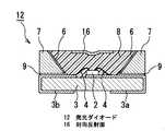
実施の形態1
まず、本発明の発光ダイオードの実施の形態1について、図1及び図2を参照して説明する。図1(a)は本発明の実施の形態1にかかる発光ダイオードの全体構成を示す平面図、(b)は縦断面図である。図2は本発明の実施の形態1にかかる発光ダイオードの光路を示す光路図である。
【0021】
図1に示されるように、本実施の形態1の発光ダイオード1は、青色発光素子(以下、単に「発光素子」ともいう。)2に電力を供給するリードをガラスエポキシ基板3に銅箔パターン3a,3bをプリントして作製している。このうち銅箔パターン3aの先端に発光素子2がマウントされ、発光素子2の上面の2個の電極がそれぞれワイヤ4によって銅箔パターン3a,3bに接続されている。さらに、ガラスエポキシ基板3の外周部分には、銅箔パターン3a,3bとの間に白色高反射レジスト9を挟んでアルミ材からなる側面側反射部材7が固定されている。この側面側反射部材7の内周には傾斜面7aからなる高反射率の反射面が形成されており、内部は光透過性材料としての透明エポキシ樹脂8で封止されている。そして、発光素子2の発光面と対向する中心部分には対向反射面としてのアルミ板からなる対向反射鏡5が高反射率の反射面を下にして配置されており、反射面には蛍光体層としての蛍光体混入樹脂6が一面に塗布されている。
【0022】
かかる構成を有する本実施の形態1の発光ダイオード1における白色光の発光時の光路について、図2を参照して説明する。
【0023】
図2に示されるように、発光素子2から対向反射面5に照射された青色光2aは、対向反射面5の表面の蛍光体混入樹脂6に含まれる蛍光体を励起して黄色系励起光6aを発生させる。発生した黄色系励起光6aのうち側面側反射部材7へ向かった光は、傾斜面7aで上方に反射されて外部へ放射される。また、発光素子2から透明エポキシ樹脂8の界面に照射された光は全反射されて側面側反射部材7に至り、傾斜面7aで上方に反射されて青色光2aのまま外部へ放射される。さらに、発光素子2から直接側面側反射部材7に至り、傾斜面7aで反射された青色光2aの大部分は上方へ反射されて外部放射されるが、一部の青色光2aは対向反射面5へ向かい、表面の蛍光体混入樹脂6に当って黄色系励起光6aを発生させる。
【0024】
このように、LED1においては蛍光体層としての蛍光体混入樹脂6が発光素子2に密接していないため、発光素子2内へ戻り吸収される青色光2a及び黄色系励起光6aの割合を極端に減らすことができる。また、蛍光体層6が対向反射面5上に形成され、この蛍光体層6に発光素子2から青色光2aが照射され、照射面から黄色系励起光6aを放射するため、蛍光体層6で吸収される青色光2a及び黄色系励起光6aの量が軽減される。このようにして、効率良く外部放射された青色光2aと黄色系励起光6aが混合されて白色光となり、LED1は輝度の高い白色光源となる。
【0025】
青色光2aは蛍光体層6表面で多く反射されるので、蛍光体層6内での吸収が少ない。また、蛍光体層6表面で、多くの光が励起されるので、黄色系励起光6aは外部へ放射され易く、吸収が少ない。
【0026】
実施の形態2
次に、本発明の発光ダイオードの実施の形態2について、図3を参照して説明する。図3は本発明の実施の形態2にかかる発光ダイオードを示す縦断面図である。なお、実施の形態1の図1と同一の部分には同一の符号を付して説明を省略する。
【0027】
図3に示されるように、本実施の形態2の発光ダイオード11が実施の形態1の発光ダイオード1と異なるのは、対向反射面を形成する対向反射鏡15が下へ凸状に湾曲している点である。これによって、側面側反射部材7へ向かう青色光及び黄色系励起光の割合が増加して、傾斜面7aで上方へ反射されて外部放射される青色光と黄色系励起光の光量が多くなるため、LED11はより輝度の高い白色光源となる。
【0028】
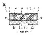
実施の形態3
次に、本発明の発光ダイオードの実施の形態3について、図4を参照して説明する。図4は本発明の実施の形態3にかかる発光ダイオードを示す縦断面図である。なお、実施の形態1の図1と同一の部分には同一の符号を付して説明を省略する。
【0029】
図4に示されるように、本実施の形態3の発光ダイオード12が実施の形態1の発光ダイオード1と異なるのは、蛍光体層としての蛍光体混入樹脂6が側面側反射部材7の反射面に塗布されている点と、対向反射面としての対向反射鏡16の中央部分が下へ凸状に湾曲している点である。
【0030】
これによって、発光素子2から対向反射鏡16に照射される青色光は大部分が側面側反射部材7へ反射され、対向反射鏡16の外側に外れた青色光も、透明エポキシ樹脂8の界面で全反射されて側面側反射部材7へ向かう。このように、発光素子2から発せられる青色光の大部分が側面側反射部材7へ向かい、側面側反射部材7の反射面には蛍光体層としての蛍光体混入樹脂6が塗布されているので、蛍光体層6へ照射された青色光によって照射面から黄色系励起光を放射するため、蛍光体層6で吸収される青色光及び黄色系励起光の量が軽減される。しかも、側面側反射部材7の反射面で反射された青色光及び黄色系励起光の大部分が対向反射鏡16の周囲の透明エポキシ樹脂8の界面から外部放射される。
【0031】
このようにして、本実施の形態3のLED12は、蛍光体混入樹脂6が塗布されている側面側反射部材7の反射面へ発光素子2の発する青色光の大部分が照射されることによって、外部放射効率が高く輝度の高い白色光源となる。
【0032】
実施の形態4
次に、本発明の発光ダイオードの実施の形態4について、図5を参照して説明する。図5は本発明の実施の形態4にかかる発光ダイオードを示す縦断面図である。なお、実施の形態3の図4と同一の部分には同一の符号を付して説明を省略する。
【0033】
図5に示されるように、本実施の形態4の発光ダイオード13が実施の形態3の発光ダイオード12と異なるのは、蛍光体層としての蛍光体混入樹脂6が側面側反射部材7の反射面のみでなく、対向反射面としての対向反射鏡16の反射面(下面)にも塗布されている点である。
【0034】
これによって、発光素子2から対向反射鏡16に照射される青色光は蛍光体層6に照射されて照射面から黄色系励起光を放射するため、蛍光体層6で吸収される青色光及び黄色系励起光の量が軽減される。対向反射鏡16で反射された青色光は大部分が側面側反射部材7へ反射され、対向反射鏡16の外側に外れた青色光も、透明エポキシ樹脂8の界面で全反射されて側面側反射部材7へ向かう。側面側反射部材7の反射面には蛍光体層としての蛍光体混入樹脂6が塗布されているので、蛍光体層6へ照射された青色光によって照射面から黄色系励起光を放射するため、蛍光体層6で吸収される青色光及び黄色系励起光の量が軽減される。しかも、側面側反射部材7の反射面で反射された青色光及び黄色系励起光の大部分が対向反射鏡16の周囲の透明エポキシ樹脂8の界面から外部放射される。
【0035】
このように、本実施の形態4のLED13においては、発光素子2から放射される青色光が二度にわたって蛍光体層6に照射された後、外部放射されるので、黄色系励起光の量が増して外部放射光の波長が長波長側へシフトする。また、二度にわたって蛍光体層6に照射されることによって、色の再現性が良好になる。さらに、側面側反射部材7及び対向反射鏡16の蛍光体層6の厚みを加減することによって、側面側反射部材7または対向反射鏡16でそのまま反射される青色光の割合を変えることができ、LED13から放射される光の色目を容易に変化させることができる。これによって、白色のみでなく赤色、緑色、青色を始めとして種々の色の光を出すことができる発光ダイオードとなる。
【0036】
上記各実施の形態においては、発光素子として青色発光素子を用い、蛍光体として青色光によって黄色系の蛍光を励起する蛍光体を用いた場合について説明したが、蛍光体を励起できる波長のものであれば、紫外線発光素子をも含めて何色の発光素子を用いても良く、何色の蛍光を発する蛍光体を用いても構わない。また、LEDにおいて発光素子等を封止する光透過性材料として透明エポキシ樹脂を用いているが、透明シリコン樹脂を始めとするその他の材料を用いても良い。
【0037】
さらに、金属反射面として高反射率のアルミ板を用いた例について説明したが、他の金属板や金属蒸着膜を用いることもできる。また、対向反射面及び側面側反射部材の材料としてアルミ材を使用した例について説明しているが、他の金属を始めとして、反射率の高い材料であれば如何なる材料を使用しても良い。
【0038】
さらに、上記各実施の形態に特有の効果として、ガラスエポキシ基板3に銅箔3a,3bをプリントしてリード部分を構成しているために、表面実装が容易に行えるという利点がある。
【0039】
発光ダイオードのその他の部分の構成、形状、数量、材質、大きさ、接続関係等についても、上記各実施の形態に限定されるものではない。
【0040】
【発明の効果】
以上説明したように、請求項1の発明にかかる発光ダイオードは、発光素子と、前記発光素子を封止する光透過性材料と、前記発光素子の発光面に対向する中心部分に配置されている金属反射面からなる対向反射面と、前記発光素子の周囲に配設された反射面を傾斜面とした側面側反射部材とを具備し、前記側面側反射部材の反射面には蛍光体層を有し、前記発光素子から前記対向反射面に照射された光のうち前記側面側反射部材側に反射した光は前記傾斜面で反射されて外部へ放射され、また、前記発光素子から前記光透過性材料の界面方向に照射された光は全反射されて前記側面側反射部材に至り、前記傾斜面で反射されて外部へ放射され、そして、前記発光素子から直接前記側面側反射部材に至る光は前記傾斜面で反射され、その大部分は外部に放射されるものである。
【0041】
これによって、発光素子から発せられた光は対向反射面で反射され、側面側反射部材でさらに反射されて外部放射される。ここで、対向反射面、側面側反射部材のいずれかの反射面に蛍光体層が設けられているため、発光素子の光で蛍光が励起されて両方の光が混ぜられて所定の色の光となって外部放射される。発光素子と蛍光体層が離れているので、蛍光体で反射された発光素子の光も励起光も発光素子へ戻って吸収される割合は格段に小さくなる。また、蛍光体層が反射材料上に形成され、蛍光体層へ光を照射し、照射面から励起光を放射するため、蛍光体層で吸収される発光素子の光も励起光も格段に少なくなる。
【0042】
このようにして、発光素子と蛍光体層を密接させないことによって、発光素子へ戻って吸収される発光素子の光及び励起光の量を少なくするとともに、蛍光体層を反射材料上に形成することによって蛍光体層で吸収される発光素子の光及び励起光の量を少なくした発光ダイオードとなる。
【0043】
そして、前記発光素子を封止する光透過性材料を有するものであるから、発光素子から放射される光量は封止されていない場合の約2倍になるので、蛍光体層で励起される蛍光の量も約2倍になり、発光ダイオードから外部放射される光量も大幅に増加する。また、封止されることによって発光素子の寿命も向上する。
【0044】
このようにして、放射される光量が多く、発光素子の寿命も長い優れた発光ダイオードとなる。
【0045】
また、前記対向反射面は前記光透過性材料の界面反射を利用したものである。即ち、発光素子の発光面から放射される光のうち、光透過性材料の界面に垂直に近く入射する光はそのまま界面から外部放射されるが、光透過性材料の界面に対して臨界角以上に斜めに入射する光は界面で全反射されて側面側反射部材へ向かう。また、臨界角以上でなくても斜めに入射する光の一部は同様に界面で反射される。このように、対向反射面として光透過性材料の界面を利用することによって、請求項2に記載の効果に加えて、対向反射面を金属材料等で新たに作製する必要がなくなるので、作製が容易になる。
【0046】
このようにして、対向反射面として光透過性材料の界面を利用することによって、作製が容易な発光ダイオードとなる。
また、前記対向反射面は金属反射面であるから、かかる金属反射面は反射率が高いので、発光素子の発光面から放射された光を小さな反射損失で側面側反射部材へ向かわせることができる。したがって、蛍光体層における励起光の発生も多くなり、外部放射される発光素子の光及び励起光の光量も大きくなる。よって、反射率の高い金属反射面を用いることによって外部放射効率の一段と高い発光ダイオードとなる。
【0047】
請求項2の発明にかかる発光ダイオードは、請求項1の構成において、対向反射鏡の前記対向反射面を前記発光素子側に凸状に湾曲させてものである。
【0048】
請求項1に記載の効果に加えて、発光素子から対向反射鏡に照射される光は大部分が側面側反射部材へ反射され、対向反射鏡の外側に外れた光も、透明エポキシ樹脂の界面で全反射されて側面側反射部材へ向かうから、効率のよい発光ダイオードとなる。
【0049】
請求項3の発明にかかる発光ダイオードは、請求項1または請求項2の構成において、前記対向反射面の反射面に前記蛍光体層を有するものである。
【0050】
請求項1または請求項2に記載の効果に加えて、対向反射面は発光素子の発光面に対向しているので、発光素子の発する光の大部分が照射される。したがって、照射光が反射面の蛍光体層に当って励起される蛍光の光量も多くなる。
【0051】
このようにして、励起される蛍光の光量が多くなる発光ダイオードとなる。
【図面の簡単な説明】
【図1】 図1(a)は本発明の実施の形態1にかかる発光ダイオードの全体構成を示す平面図、(b)は縦断面図である。
【図2】 図2は本発明の実施の形態1にかかる発光ダイオードの光路を示す光路図である。
【図3】 図3は本発明の実施の形態2にかかる発光ダイオードを示す縦断面図である。
【図4】 図4は本発明の実施の形態3にかかる発光ダイオードを示す縦断面図である。
【図5】 図5は本発明の実施の形態4にかかる発光ダイオードを示す縦断面図である。
【符号の説明】
1,11,12,13 発光ダイオード
2 発光素子
5,15,16 対向反射面
6 蛍光体層
7 側面側反射部材
7a 傾斜面
8 光透過性材料[0001]
BACKGROUND OF THE INVENTION
The present invention relates to a light emitting diode in which a reflection surface is provided around a light emitting element, and a phosphor layer is provided on the reflection surface, thereby reducing the absorbed light and increasing the external radiation efficiency.
[0002]
In the present specification, the LED chip itself is referred to as a “light emitting element”, and the whole including the optical device such as a package resin or a lens system on which the LED chip is mounted is referred to as a “light emitting diode” or “LED”. To do.
[0003]
[Prior art]
2. Description of the Related Art Conventionally, there is a white light source that forms white light by sealing a blue light emitting element with a transparent resin containing a phosphor and mixing blue light emitted from the blue light emitting element and yellow excitation light emitted from the phosphor. In such a structure, the absorption by the blue light emitting element and the absorption by the phosphor are large, and the light efficiency is low. That is, some of the light emitted from the blue light emitting element is reflected by the phosphor and returns to the blue light emitting element. The blue light emitting element has a high refractive index, so it is difficult to be emitted to the outside again, and the light absorption rate is high. Further, the light emitted through the phosphor layer is absorbed in the phosphor layer, attenuated, and emitted outside.
[0004]
On the other hand, the side adjacent to the blue light emitting element in the phosphor layer has a high irradiation density of blue light, and the return light to the blue light emitting element out of the yellow excitation light is still difficult to be emitted to the outside, and the light absorption rate is high. Further, light emitted outside through the phosphor layer is absorbed in the layer, attenuated, and emitted outside.
[0005]
[Problems to be solved by the invention]
As described above, since the blue light emitting element and the phosphor layer are in close contact with each other, blue light emitted from the blue light emitting element and reflected by the phosphor, and yellow excitation light excited by the phosphor emit blue light. It returns to the element and is absorbed with a high absorption rate. Further, the blue light and the yellow excitation light passing through the phosphor layer are absorbed and attenuated in the layer while passing through the thick phosphor layer. From the above, the external radiation efficiency of white light generated by mixing blue light and yellow excitation light has been low.
[0006]
Therefore, the present invention reduces the amount of light and excitation light of the light emitting element that is absorbed back to the light emitting element by not bringing the light emitting element and the phosphor layer into close contact with each other, and forms the phosphor layer on the reflective material. Accordingly, an object of the present invention is to provide a light emitting diode in which the amount of light and excitation light of the light emitting element absorbed by the phosphor layer is reduced.
[0007]
[Means for Solving the Problems]
The light-emitting diode according to the invention of
[0008]
Thereby, the light emitted from the light emitting element is reflected by the opposing reflection surface, further reflected by the side surface reflection member, and radiated to the outside. Here, since the phosphor layer is provided on the reflection surface of the opposing reflection surface or the side-surface-side reflection member, the fluorescence is excited by the light of the light emitting element, and both lights are mixed and light of a predetermined color. Becomes external radiation. Since the light emitting element and the phosphor layer are separated from each other, the ratio of the light of the light emitting element reflected by the phosphor and the excitation light that is returned to the light emitting element and absorbed is significantly reduced. In addition, since the phosphor layer is formed on the reflective material, the phosphor layer is irradiated with light, and the excitation light is emitted from the irradiation surface, so that the light of the light emitting element absorbed by the phosphor layer and the excitation light are extremely small. Become.
[0009]
In this way, by not bringing the light emitting element and the phosphor layer into close contact with each other, the amount of light and excitation light of the light emitting element that is absorbed back to the light emitting element is reduced, and the phosphor layer is formed on the reflective material. Thus, a light emitting diode in which the amount of light and excitation light absorbed by the phosphor layer is reduced is obtained.
[0010]
And since it has the light transmissive material which seals the said light emitting element, since the light quantity radiated | emittedfrom a light emitting element is about twice as much as the case where it is not sealed, the quantity of the fluorescence excited by a fluorescent substance layer is also The amount of light emitted from the light emitting diode is increased substantially by a factor of about two. In addition, the lifetime of the light emitting element is improved by sealing.
[0011]
In this manner, an excellent light-emitting diode that emits a large amount of light and has a long lifetime of the light-emitting element is obtained.
[0012]
Furthermore, the opposing reflection surface utilizes interface reflection of the light transmissive material. That is, of the light emitted from the light emitting surface of the light emitting element, the light that is incident perpendicularly to the interface of the light transmissive material is radiated externally from the interface as it is, but it is above the critical angle with respect to the interface of the light transmissive material. Light obliquely incident on the light is totally reflected at the interface and travels to the side-surface reflecting member. Even if the angle is not greater than the critical angle, a part of the incident light is reflected at the interface in the same manner. As described above, by using the interface of the light transmissive material as the counter reflecting surface, it is not necessary to newly manufacture the counter reflecting surface with a metal material or the like, so that the manufacturing becomes easy. Examples of themetal reflecting surface include a metal plate such as an aluminum plate and a metal vapor deposition film. Since such a metal reflecting surface has a high reflectance, light emitted from the light emitting surface of the light emitting element can be directed to the side reflecting member with a small reflection loss. Accordingly, the generation of excitation light in the phosphor layer is increased, and the amount of light emitted from the light emitting element and the amount of excitation light is increased. In this way, a light emitting diode with higher external radiation efficiency is obtained by using a metal reflecting surface having a high reflectance.
[0013]
In this manner, a light-emitting diode that is easy to manufacture is obtained by utilizing the interface of the light-transmitting material as the counter-reflection surface.
[0014]
According to a second aspect of the present invention, there is provided a light emitting diodeaccording to the firstaspect, wherein the counter reflecting surface of thecounter reflecting mirror is curved in a convex shape toward the light emitting element.
[0015]
As a result, most of the light radiated from the light emitting element to the opposing reflecting mirror is reflected to the side reflecting member, and the light that has gone outside the opposing reflecting mirror is also totally reflected at the interface of the transparent epoxy resin and reflected from the side. Head to the member.
[0016]
A light-emitting diode according to athird aspect of the present invention is the light-emitting diode according to thefirst or second aspect, wherein the phosphor layer is provided on the reflection surface of the opposing reflection surface.
[0017]
Since the opposing reflecting surface faces the light emitting surface of the light emitting element, most of the light emitted from the light emitting element is irradiated. Accordingly, the amount of fluorescent light that is excited when the irradiated light strikes the phosphor layer on the reflecting surface also increases.
[0018]
In this way, a light emitting diode in which the amount of excited fluorescence is increased.
[0019]
DETAILED DESCRIPTION OF THE INVENTION
Hereinafter, embodiments of the present invention will be described with reference to the drawings.
[0020]
First,
[0021]
As shown in FIG. 1, the light-emitting
[0022]
An optical path at the time of light emission of white light in the light-emitting
[0023]
As shown in FIG. 2, the
[0024]
As described above, in the
[0025]
Since the
[0026]
Next, a second embodiment of the light emitting diode of the present invention will be described with reference to FIG. FIG. 3 is a longitudinal sectional view showing a light emitting diode according to a second embodiment of the present invention. In addition, the same code | symbol is attached | subjected to the part same as FIG. 1 of
[0027]
As shown in FIG. 3, the light-emitting
[0028]
Next, a third embodiment of the light emitting diode of the present invention will be described with reference to FIG. FIG. 4 is a longitudinal sectional view showing a light emitting diode according to a third embodiment of the present invention. In addition, the same code | symbol is attached | subjected to the part same as FIG. 1 of
[0029]
As shown in FIG. 4, the
[0030]
As a result, most of the blue light emitted from the
[0031]
In this way, the
[0032]
Next, a fourth embodiment of the light emitting diode of the present invention will be described with reference to FIG. FIG. 5 is a longitudinal sectional view showing a light emitting diode according to a fourth embodiment of the present invention. In addition, the same code | symbol is attached | subjected to the part same as FIG. 4 of
[0033]
As shown in FIG. 5, the light-emitting
[0034]
Thereby, the blue light irradiated from the
[0035]
Thus, in LED13 of this
[0036]
In each of the above embodiments, a case where a blue light emitting element is used as a light emitting element and a phosphor that excites yellow fluorescence by blue light is used as a phosphor has been described. If so, any color light-emitting element including an ultraviolet light-emitting element may be used, and any color fluorescent substance may be used. Further, although a transparent epoxy resin is used as a light transmissive material for sealing a light emitting element or the like in an LED, other materials such as a transparent silicon resin may be used.
[0037]
Furthermore, although the example which used the aluminum plate of the high reflectance as a metal reflective surface was demonstrated, another metal plate and a metal vapor deposition film can also be used. Moreover, although the example which used the aluminum material as a material of an opposing reflective surface and a side surface side reflection member is demonstrated, what kind of material may be used if it is a material with high reflectance including another metal.
[0038]
Further, as an effect peculiar to each of the above embodiments, there is an advantage that the surface mounting can be easily performed because the lead portions are configured by printing the copper foils 3a and 3b on the
[0039]
The configuration, shape, quantity, material, size, connection relationship, and the like of the other parts of the light emitting diode are not limited to the above embodiments.
[0040]
【The invention's effect】
As described above, the light emitting diode according to the first aspect of the present invention isdisposed in the light emitting element, the light-transmitting material that seals the light emitting element, and the central portion that faces the light emitting surface of the light emitting element. A counter-reflection surface made of a metal reflection surface; and a side-surface-side reflection member having a reflection surface disposed around the light-emitting element as an inclined surface, and a phosphor layer is provided on the reflection surface of the side-surface-side reflection member And the light reflected from the light emitting element to the opposing reflecting surface is reflected by the inclined surface and radiated to the outside, and the light is transmitted from the light emitting element. The light irradiated in the interface direction of the conductive material is totally reflected to reach the side surface reflecting member, is reflected by the inclined surface and radiated to the outside, and the light directly reaches the side surface reflecting member from the light emitting element. Is reflected by the inclined surface, most of which It is intended to be emitted to the outside.
[0041]
Thereby, the light emitted from the light emitting element is reflected by the opposing reflection surface, further reflected by the side surface reflection member, and radiated to the outside. Here, since the phosphor layer is provided on the reflection surface of the opposing reflection surface or the side-surface-side reflection member, the fluorescence is excited by the light of the light emitting element, and both lights are mixed and light of a predetermined color. Becomes external radiation. Since the light emitting element and the phosphor layer are separated from each other, the ratio of the light of the light emitting element reflected by the phosphor and the excitation light that is returned to the light emitting element and absorbed is significantly reduced. In addition, since the phosphor layer is formed on the reflective material, the phosphor layer is irradiated with light, and the excitation light is emitted from the irradiation surface, so that the light of the light emitting element absorbed by the phosphor layer and the excitation light are extremely small. Become.
[0042]
In this way, by not bringing the light emitting element and the phosphor layer into close contact with each other, the amount of light and excitation light of the light emitting element that is absorbed back to the light emitting element is reduced, and the phosphor layer is formed on the reflective material. Thus, a light emitting diode in which the amount of light and excitation light absorbed by the phosphor layer is reduced is obtained.
[0043]
Since the light-transmitting material that seals the light-emitting element is used, the amount of light emittedfrom the light-emitting element is approximately twice that of the case where the light-emitting element is not sealed. The amount of light is also doubled, and the amount of light emitted from the light emitting diode is greatly increased. In addition, the lifetime of the light emitting element is improved by sealing.
[0044]
In this manner, an excellent light-emitting diode that emits a large amount of light and has a long lifetime of the light-emitting element is obtained.
[0045]
Moreover, the said opposing reflective surface utilizes the interface reflection of the said light transmissive material. That is, of the light emitted from the light emitting surface of the light emitting element, the light that is incident perpendicularly to the interface of the light transmissive material is radiated externally from the interface as it is, but it is above the critical angle with respect to the interface of the light transmissive material. Light obliquely incident on the light is totally reflected at the interface and travels to the side-surface reflecting member. Even if the angle is not greater than the critical angle, a part of the incident light is reflected at the interface in the same manner. In this way, by using the interface of the light transmissive material as the counter reflecting surface, in addition to the effect of
[0046]
In this manner, a light-emitting diode that is easy to manufacture is obtained by utilizing the interface of the light-transmitting material as the counter-reflection surface.
In addition, since the opposing reflecting surface is a metal reflecting surface, the metal reflecting surface has high reflectivity, and thus light emitted from the light emitting surface of the light emitting element can be directed to the side reflecting member with a small reflection loss. . Accordingly, the generation of excitation light in the phosphor layer is increased, and the amount of light emitted from the light emitting element and the amount of excitation light is increased. Therefore, by using a metal reflecting surface having a high reflectance, a light emitting diode with a higher external radiation efficiency is obtained.
[0047]
According to a second aspect of the present invention, there is provided a light emitting diodeaccording to the firstaspect, wherein the counter reflecting surface of thecounter reflecting mirror is curved in a convex shape toward the light emitting element.
[0048]
In addition to the effect according to
[0049]
A light-emitting diode according to athird aspect of the present invention is the light-emitting diode according to thefirst or second aspect, wherein the phosphor layer is provided on the reflection surface of the opposing reflection surface.
[0050]
In addition to the effect described in
[0051]
In this way, a light emitting diode in which the amount of excited fluorescence is increased.
[Brief description of the drawings]
FIG. 1A is a plan view showing an overall configuration of a light emitting diode according to a first embodiment of the present invention, and FIG. 1B is a longitudinal sectional view thereof.
FIG. 2 is an optical path diagram showing an optical path of the light emitting diode according to the first embodiment of the present invention.
FIG. 3 is a longitudinal sectional view showing a light emitting diode according to a second embodiment of the present invention.
FIG. 4 is a longitudinal sectional view showing a light emitting diode according to a third embodiment of the present invention.
FIG. 5 is a longitudinal sectional view showing a light emitting diode according to a fourth embodiment of the present invention.
[Explanation of symbols]
1, 11, 12, 13
Claims (3)
Translated fromJapanese前記側面側反射部材の反射面には蛍光体層を有し、前記発光素子から前記対向反射面に照射された光のうち前記側面側反射部材側に反射した光は前記傾斜面で反射されて外部へ放射され、また、前記発光素子から前記光透過性材料の界面方向に照射された光は全反射されて前記側面側反射部材に至り、前記傾斜面で反射されて外部へ放射され、そして、前記発光素子から直接前記側面側反射部材に至る光は前記傾斜面で反射され、その大部分は外部に放射されることを特徴とする発光ダイオード。A light-emitting element,a light-transmitting material that seals the light- emitting element,a counter-reflecting surface including ametal reflecting surface that is disposed at acentral portion facing the light-emitting surface of the light-emitting element, and a periphery of the light-emitting element A side-surface- side reflecting member havingan inclined reflecting surface provided,
The reflecting surface of the side-surface reflecting member has a phosphor layer, and light reflected from the light emitting element to the opposing reflecting surface toward the side-surface reflecting member is reflected by the inclined surface. The light emitted to the outside and irradiated from the light emitting element toward the interface of the light transmissive material is totally reflected to reach the side reflection member, reflected by the inclined surface and emitted to the outside, and The light directly from the light emitting element to the side surface reflecting member is reflected by the inclined surface, and most of the light is emitted to the outside .
Priority Applications (2)
| Application Number | Priority Date | Filing Date | Title |
|---|---|---|---|
| JP2002103977AJP4172196B2 (en) | 2002-04-05 | 2002-04-05 | Light emitting diode |
| US10/393,024US7279719B2 (en) | 2002-04-05 | 2003-03-21 | Light emitting diode |
Applications Claiming Priority (1)
| Application Number | Priority Date | Filing Date | Title |
|---|---|---|---|
| JP2002103977AJP4172196B2 (en) | 2002-04-05 | 2002-04-05 | Light emitting diode |
Publications (2)
| Publication Number | Publication Date |
|---|---|
| JP2003298117A JP2003298117A (en) | 2003-10-17 |
| JP4172196B2true JP4172196B2 (en) | 2008-10-29 |
Family
ID=29242805
Family Applications (1)
| Application Number | Title | Priority Date | Filing Date |
|---|---|---|---|
| JP2002103977AExpired - Fee RelatedJP4172196B2 (en) | 2002-04-05 | 2002-04-05 | Light emitting diode |
Country Status (2)
| Country | Link |
|---|---|
| US (1) | US7279719B2 (en) |
| JP (1) | JP4172196B2 (en) |
Families Citing this family (108)
| Publication number | Priority date | Publication date | Assignee | Title |
|---|---|---|---|---|
| JP3707688B2 (en)* | 2002-05-31 | 2005-10-19 | スタンレー電気株式会社 | Light emitting device and manufacturing method thereof |
| US7244965B2 (en) | 2002-09-04 | 2007-07-17 | Cree Inc, | Power surface mount light emitting die package |
| US7264378B2 (en) | 2002-09-04 | 2007-09-04 | Cree, Inc. | Power surface mount light emitting die package |
| US7775685B2 (en) | 2003-05-27 | 2010-08-17 | Cree, Inc. | Power surface mount light emitting die package |
| JP3910517B2 (en)* | 2002-10-07 | 2007-04-25 | シャープ株式会社 | LED device |
| US6897486B2 (en) | 2002-12-06 | 2005-05-24 | Ban P. Loh | LED package die having a small footprint |
| US7692206B2 (en) | 2002-12-06 | 2010-04-06 | Cree, Inc. | Composite leadframe LED package and method of making the same |
| CN101740560B (en) | 2003-04-01 | 2012-11-21 | 夏普株式会社 | Light-emitting apparatus, backlight apparatus, and display apparatus |
| US7777235B2 (en)* | 2003-05-05 | 2010-08-17 | Lighting Science Group Corporation | Light emitting diodes with improved light collimation |
| US8999736B2 (en)* | 2003-07-04 | 2015-04-07 | Epistar Corporation | Optoelectronic system |
| US6995402B2 (en)* | 2003-10-03 | 2006-02-07 | Lumileds Lighting, U.S., Llc | Integrated reflector cup for a light emitting device mount |
| US7517728B2 (en)* | 2004-03-31 | 2009-04-14 | Cree, Inc. | Semiconductor light emitting devices including a luminescent conversion element |
| US7837348B2 (en) | 2004-05-05 | 2010-11-23 | Rensselaer Polytechnic Institute | Lighting system using multiple colored light emitting sources and diffuser element |
| AU2005240186B2 (en) | 2004-05-05 | 2011-02-03 | Rensselaer Polytechnic Institute | High efficiency light source using solid-state emitter and down-conversion material |
| JP2005347467A (en)* | 2004-06-02 | 2005-12-15 | Fujikura Ltd | LIGHT EMITTING DEVICE AND LIGHTING DEVICE |
| US7456499B2 (en) | 2004-06-04 | 2008-11-25 | Cree, Inc. | Power light emitting die package with reflecting lens and the method of making the same |
| DE102005030128B4 (en)* | 2004-06-28 | 2011-02-03 | Kyocera Corp. | Light-emitting device and lighting device |
| JP2006066657A (en)* | 2004-08-27 | 2006-03-09 | Kyocera Corp | Light emitting device and lighting device |
| JP2006049814A (en)* | 2004-06-28 | 2006-02-16 | Kyocera Corp | Light emitting device and lighting device |
| DE102004045947A1 (en)* | 2004-06-30 | 2006-01-19 | Osram Opto Semiconductors Gmbh | LED array |
| CN100521266C (en)* | 2004-08-06 | 2009-07-29 | 皇家飞利浦电子股份有限公司 | LED lamp system |
| JP4624069B2 (en)* | 2004-10-27 | 2011-02-02 | 京セラ株式会社 | LIGHT EMITTING DEVICE, ITS MANUFACTURING METHOD, AND LIGHTING DEVICE |
| JP4615981B2 (en)* | 2004-12-08 | 2011-01-19 | スタンレー電気株式会社 | Light emitting diode and manufacturing method thereof |
| KR100610278B1 (en) | 2004-12-14 | 2006-08-09 | 알티전자 주식회사 | High Brightness White Light Emitting Diode and Manufacturing Method Thereof |
| JP4748411B2 (en)* | 2005-01-06 | 2011-08-17 | 株式会社フジクラ | Light emitting device, method for adjusting chromaticity of light emitting device, and lighting apparatus |
| US7777247B2 (en) | 2005-01-14 | 2010-08-17 | Cree, Inc. | Semiconductor light emitting device mounting substrates including a conductive lead extending therein |
| WO2006099741A1 (en)* | 2005-03-24 | 2006-09-28 | Tir Systems Ltd. | Solid-state lighting device package |
| WO2006105638A1 (en)* | 2005-04-05 | 2006-10-12 | Tir Systems Ltd. | Electronic device package with an integrated evaporator |
| CN100409462C (en)* | 2005-05-26 | 2008-08-06 | 陈隆建 | Reflection type white light emitting diode excited by fluorescent powder |
| JP4992282B2 (en)* | 2005-06-10 | 2012-08-08 | ソニー株式会社 | Light emitting diode, light emitting diode manufacturing method, light emitting diode backlight, light emitting diode illumination device, light emitting diode display, and electronic device |
| US7980743B2 (en) | 2005-06-14 | 2011-07-19 | Cree, Inc. | LED backlighting for displays |
| CA2597697C (en)* | 2005-06-23 | 2014-12-02 | Rensselaer Polytechnic Institute | Package design for producing white light with short-wavelength leds and down-conversion materials |
| US7293908B2 (en)* | 2005-10-18 | 2007-11-13 | Goldeneye, Inc. | Side emitting illumination systems incorporating light emitting diodes |
| KR101241650B1 (en) | 2005-10-19 | 2013-03-08 | 엘지이노텍 주식회사 | Package of light emitting diode |
| JP5209177B2 (en)* | 2005-11-14 | 2013-06-12 | 新光電気工業株式会社 | Semiconductor device and manufacturing method of semiconductor device |
| JP4771800B2 (en)* | 2005-12-02 | 2011-09-14 | スタンレー電気株式会社 | Semiconductor light emitting device and manufacturing method thereof |
| TWI326378B (en)* | 2005-12-16 | 2010-06-21 | Chimei Innolux Corp | Light emitting diode and back light module using the same |
| JP2007180203A (en)* | 2005-12-27 | 2007-07-12 | Shinko Electric Ind Co Ltd | Semiconductor device and manufacturing method of semiconductor device |
| US8044412B2 (en) | 2006-01-20 | 2011-10-25 | Taiwan Semiconductor Manufacturing Company, Ltd | Package for a light emitting element |
| US20070181897A1 (en)* | 2006-02-03 | 2007-08-09 | Been-Yu Liaw | High heat dissipating package baseplate for a high brightness LED |
| JP4838005B2 (en)* | 2006-02-20 | 2011-12-14 | 京セラ株式会社 | Light emitting device |
| JP5420141B2 (en)* | 2006-03-01 | 2014-02-19 | 東レ・ダウコーニング株式会社 | Curable silicone resin composition and cured product |
| US7977692B2 (en)* | 2006-03-31 | 2011-07-12 | Avago Technologies General Ip (Singapore) Pte. Ltd. | SMT LED with high light output for high power applications |
| US9502624B2 (en) | 2006-05-18 | 2016-11-22 | Nichia Corporation | Resin molding, surface mounted light emitting apparatus and methods for manufacturing the same |
| KR101496066B1 (en)* | 2006-06-02 | 2015-03-02 | 히타치가세이가부시끼가이샤 | Optical semiconductor element mounting package, and optical semiconductor device using the same |
| JP4611937B2 (en)* | 2006-06-07 | 2011-01-12 | 日亜化学工業株式会社 | Surface mount type light emitting device and manufacturing method thereof |
| US7703945B2 (en)* | 2006-06-27 | 2010-04-27 | Cree, Inc. | Efficient emitting LED package and method for efficiently emitting light |
| US7906794B2 (en)* | 2006-07-05 | 2011-03-15 | Koninklijke Philips Electronics N.V. | Light emitting device package with frame and optically transmissive element |
| US7703942B2 (en) | 2006-08-31 | 2010-04-27 | Rensselaer Polytechnic Institute | High-efficient light engines using light emitting diodes |
| KR20090057114A (en)* | 2006-09-27 | 2009-06-03 | 가부시끼가이샤 도시바 | Semiconductor light emitting device, backlight and display device comprising the semiconductor light emitting device |
| BRPI0718086A2 (en)* | 2006-10-31 | 2013-11-05 | Tir Technology Lp | LIGHTING DEVICE PACKAGING |
| US7889421B2 (en) | 2006-11-17 | 2011-02-15 | Rensselaer Polytechnic Institute | High-power white LEDs and manufacturing method thereof |
| TW200824150A (en)* | 2006-11-29 | 2008-06-01 | Solidlite Corp | Package structure of light emitting diode having high divergence angle |
| EP1928026A1 (en)* | 2006-11-30 | 2008-06-04 | Toshiba Lighting & Technology Corporation | Illumination device with semiconductor light-emitting elements |
| JP5380774B2 (en) | 2006-12-28 | 2014-01-08 | 日亜化学工業株式会社 | Surface mount type side surface light emitting device and manufacturing method thereof |
| JP4264109B2 (en)* | 2007-01-16 | 2009-05-13 | 株式会社東芝 | Light emitting device |
| US20090085053A1 (en)* | 2007-01-25 | 2009-04-02 | Hsing Chen | Light emitting diode package with large viewing angle |
| JP2008205170A (en)* | 2007-02-20 | 2008-09-04 | Nec Lighting Ltd | Light emitting semiconductor device |
| US20080198572A1 (en)* | 2007-02-21 | 2008-08-21 | Medendorp Nicholas W | LED lighting systems including luminescent layers on remote reflectors |
| TWI326923B (en)* | 2007-03-07 | 2010-07-01 | Lite On Technology Corp | White light emitting diode |
| WO2008129945A1 (en) | 2007-04-17 | 2008-10-30 | Nikon Corporation | Illuminating device, projector and camera |
| US7942556B2 (en)* | 2007-06-18 | 2011-05-17 | Xicato, Inc. | Solid state illumination device |
| US20090008662A1 (en)* | 2007-07-05 | 2009-01-08 | Ian Ashdown | Lighting device package |
| JP2009071254A (en)* | 2007-08-23 | 2009-04-02 | Panasonic Electric Works Co Ltd | Light emitting device |
| US7810956B2 (en)* | 2007-08-23 | 2010-10-12 | Koninklijke Philips Electronics N.V. | Light source including reflective wavelength-converting layer |
| US8866185B2 (en)* | 2007-09-06 | 2014-10-21 | SemiLEDs Optoelectronics Co., Ltd. | White light LED with multiple encapsulation layers |
| EP2193554B1 (en)* | 2007-09-20 | 2015-12-02 | Philips Intellectual Property & Standards GmbH | Light emitting diode package |
| KR100854915B1 (en)* | 2007-10-04 | 2008-08-27 | 정숙자 | Manufacturing method of epoxy resin block containing light emitting diode |
| US8946987B2 (en)* | 2007-11-07 | 2015-02-03 | Industrial Technology Research Institute | Light emitting device and fabricating method thereof |
| DE102007056874A1 (en)* | 2007-11-26 | 2009-05-28 | Osram Gesellschaft mit beschränkter Haftung | LED lighting device with conversion reflector |
| JP2009130301A (en)* | 2007-11-27 | 2009-06-11 | Sharp Corp | Light emitting device and method for manufacturing light emitting device |
| KR100954453B1 (en)* | 2008-07-04 | 2010-04-27 | (주) 아모엘이디 | LED package |
| CN101562221A (en)* | 2008-04-18 | 2009-10-21 | 富准精密工业(深圳)有限公司 | Side light emitting diode |
| WO2010029872A1 (en)* | 2008-09-09 | 2010-03-18 | 昭和電工株式会社 | Light emitting unit, light emitting module, and display device |
| TWI405356B (en)* | 2008-10-30 | 2013-08-11 | Gio Optoelectronics Corp | Light unit |
| JP2010171379A (en)* | 2008-12-25 | 2010-08-05 | Seiko Instruments Inc | Light-emitting device |
| KR101076738B1 (en) | 2009-01-09 | 2011-10-26 | 주식회사 이츠웰 | Fablication method of light emitting diode and light emitting diode using the same |
| JP5499325B2 (en)* | 2009-06-01 | 2014-05-21 | 東芝ライテック株式会社 | Light emitting module and lighting device |
| US8118454B2 (en)* | 2009-12-02 | 2012-02-21 | Abl Ip Holding Llc | Solid state lighting system with optic providing occluded remote phosphor |
| WO2011082497A1 (en)* | 2010-01-11 | 2011-07-14 | Cooledge Lighting Inc. | Package for light emitting and receiving devices |
| DE102010032302A1 (en)* | 2010-07-26 | 2012-01-26 | Osram Opto Semiconductors Gmbh | Optoelectronic semiconductor device, has reflecting element partially reflecting back emitted electromagnetic radiation in direction of semiconductor chip, and partially overlapping with main surface of chip in radiation emitting direction |
| DE102010048561A1 (en)* | 2010-10-18 | 2012-04-19 | ATMOS Medizin Technik GmbH & Co. KG | LED array with improved light output and method of operating an LED array with improved light output |
| US20120113619A1 (en)* | 2010-11-04 | 2012-05-10 | Au Optronics Corporation | Light source and backlight module having the same |
| US9057806B2 (en) | 2010-11-04 | 2015-06-16 | Au Optronics Corporation | Light source and backlight module having the same |
| JP5962102B2 (en)* | 2011-03-24 | 2016-08-03 | 日亜化学工業株式会社 | Light emitting device and manufacturing method thereof |
| US20120250320A1 (en)* | 2011-03-31 | 2012-10-04 | Xicato, Inc. | Color conversion cavities for led-based illumination modules |
| CN102760816A (en)* | 2011-04-26 | 2012-10-31 | 展晶科技(深圳)有限公司 | LED (light emitting diode) packaging structure and manufacturing method thereof |
| JP2012238830A (en) | 2011-05-09 | 2012-12-06 | Lumirich Co Ltd | Light emitting diode element |
| DE102011050450A1 (en) | 2011-05-18 | 2012-11-22 | Osram Opto Semiconductors Gmbh | Optoelectronic semiconductor chip, optoelectronic semiconductor component and method for producing an optoelectronic semiconductor component |
| KR101798884B1 (en) | 2011-05-18 | 2017-11-17 | 삼성전자주식회사 | Light emitting device assembly and head light including the same |
| EP2716967A4 (en)* | 2011-05-27 | 2015-06-10 | Olympus Corp | Light source device |
| JP2012248401A (en)* | 2011-05-27 | 2012-12-13 | Olympus Corp | Light source device |
| JP5851119B2 (en)* | 2011-05-27 | 2016-02-03 | オリンパス株式会社 | Light source device |
| KR101294488B1 (en)* | 2011-11-14 | 2013-08-07 | 엘지이노텍 주식회사 | Light emitting device |
| CN102522476B (en)* | 2011-12-23 | 2014-03-12 | 泉州万明光电有限公司 | Packaging structure of efficient light emitting diode light source |
| KR102176390B1 (en)* | 2012-03-30 | 2020-11-10 | 루미리즈 홀딩 비.브이. | Optical cavity including a light emitting device and wavelength converting material |
| KR102029802B1 (en)* | 2013-01-14 | 2019-10-08 | 엘지이노텍 주식회사 | Light emitting device and light apparatus having thereof |
| JP6094804B2 (en)* | 2013-04-02 | 2017-03-15 | 東芝ライテック株式会社 | LIGHTING DEVICE AND VEHICLE LIGHT |
| US9677918B2 (en)* | 2014-10-06 | 2017-06-13 | Continental Automotive Systems, Inc. | Light propagation and even distribution using air channels |
| US9799804B2 (en) | 2014-10-28 | 2017-10-24 | Matrix Lighting Ltd. | Light-emitting device with near full spectrum light output |
| JP6493348B2 (en)* | 2016-09-30 | 2019-04-03 | 日亜化学工業株式会社 | Light emitting device |
| US10195985B2 (en)* | 2017-03-08 | 2019-02-05 | Ford Global Technologies, Llc | Vehicle light system |
| JP6876810B2 (en)* | 2017-08-28 | 2021-05-26 | Hoya株式会社 | Light source device for endoscopes and endoscope system |
| CN110176529B (en)* | 2018-02-20 | 2022-03-08 | 晶元光电股份有限公司 | Light-emitting element and method of making the same |
| JP2019160859A (en)* | 2018-03-08 | 2019-09-19 | 豊田合成株式会社 | Light-emitting device |
| DE102018105908A1 (en) | 2018-03-14 | 2019-09-19 | Osram Opto Semiconductors Gmbh | Optoelectronic component and method for producing an optoelectronic component |
| CN110379912B (en)* | 2019-06-28 | 2021-06-22 | 佛山市国星光电股份有限公司 | LED devices, backlight modules and display devices |
| CN112349822B (en)* | 2019-08-09 | 2022-03-18 | 佛山市国星光电股份有限公司 | LED device and backlight module |
Family Cites Families (3)
| Publication number | Priority date | Publication date | Assignee | Title |
|---|---|---|---|---|
| TW383508B (en) | 1996-07-29 | 2000-03-01 | Nichia Kagaku Kogyo Kk | Light emitting device and display |
| JP3624699B2 (en)* | 1998-07-03 | 2005-03-02 | スタンレー電気株式会社 | Reflective LED lamp |
| US6155699A (en)* | 1999-03-15 | 2000-12-05 | Agilent Technologies, Inc. | Efficient phosphor-conversion led structure |
- 2002
- 2002-04-05JPJP2002103977Apatent/JP4172196B2/ennot_activeExpired - Fee Related
- 2003
- 2003-03-21USUS10/393,024patent/US7279719B2/ennot_activeExpired - Fee Related
Also Published As
| Publication number | Publication date |
|---|---|
| US7279719B2 (en) | 2007-10-09 |
| US20030201451A1 (en) | 2003-10-30 |
| JP2003298117A (en) | 2003-10-17 |
Similar Documents
| Publication | Publication Date | Title |
|---|---|---|
| JP4172196B2 (en) | Light emitting diode | |
| US6900587B2 (en) | Light-emitting diode | |
| JP4254276B2 (en) | Light emitting device and manufacturing method thereof | |
| KR101297405B1 (en) | Light emitting device employing dielectric multilayer reflecting mirror | |
| US7084435B2 (en) | Light emitting device using LED | |
| JP4182783B2 (en) | LED package | |
| JP5261380B2 (en) | Light emitting device | |
| JP6422636B2 (en) | Light source device | |
| JP5025636B2 (en) | Light emitting device | |
| US20100128463A1 (en) | Headlight for vehicle | |
| JP2001345483A (en) | Light emitting diode | |
| JP2008117666A (en) | Light emitting device and backlight device using the same | |
| JP2003110146A (en) | Light emitting device | |
| JP2007265964A (en) | Lighting device | |
| JP2003124521A (en) | Semiconductor light emitting device with case | |
| JP2008028181A (en) | Lighting device | |
| JP2007059864A (en) | LIGHTING DEVICE AND LIGHT EMITTING DIODE DEVICE | |
| KR20130112577A (en) | Led lighting apparatus | |
| JP2005191192A (en) | Light emitting element mounting substrate and light emitting device | |
| JP2008205170A (en) | Light emitting semiconductor device | |
| JP4747704B2 (en) | Method for manufacturing light emitting device with phosphor layer | |
| JP2001148509A (en) | Illuminating light source | |
| JP2001230451A (en) | Light emitting diode | |
| JP2008028182A (en) | Lighting device | |
| KR101258228B1 (en) | Light emitting device having plurality of light-converting material laters |
Legal Events
| Date | Code | Title | Description |
|---|---|---|---|
| A621 | Written request for application examination | Free format text:JAPANESE INTERMEDIATE CODE: A621 Effective date:20040924 | |
| A977 | Report on retrieval | Free format text:JAPANESE INTERMEDIATE CODE: A971007 Effective date:20070219 | |
| A131 | Notification of reasons for refusal | Free format text:JAPANESE INTERMEDIATE CODE: A131 Effective date:20070227 | |
| A521 | Request for written amendment filed | Free format text:JAPANESE INTERMEDIATE CODE: A523 Effective date:20070412 | |
| TRDD | Decision of grant or rejection written | ||
| A01 | Written decision to grant a patent or to grant a registration (utility model) | Free format text:JAPANESE INTERMEDIATE CODE: A01 Effective date:20080722 | |
| A01 | Written decision to grant a patent or to grant a registration (utility model) | Free format text:JAPANESE INTERMEDIATE CODE: A01 | |
| A61 | First payment of annual fees (during grant procedure) | Free format text:JAPANESE INTERMEDIATE CODE: A61 Effective date:20080804 | |
| R150 | Certificate of patent or registration of utility model | Free format text:JAPANESE INTERMEDIATE CODE: R150 | |
| FPAY | Renewal fee payment (event date is renewal date of database) | Free format text:PAYMENT UNTIL: 20110822 Year of fee payment:3 | |
| FPAY | Renewal fee payment (event date is renewal date of database) | Free format text:PAYMENT UNTIL: 20110822 Year of fee payment:3 | |
| FPAY | Renewal fee payment (event date is renewal date of database) | Free format text:PAYMENT UNTIL: 20120822 Year of fee payment:4 | |
| FPAY | Renewal fee payment (event date is renewal date of database) | Free format text:PAYMENT UNTIL: 20130822 Year of fee payment:5 | |
| LAPS | Cancellation because of no payment of annual fees |