JP4169150B2 - Method of forming a metal pattern using a sacrificial hard mask - Google Patents
Method of forming a metal pattern using a sacrificial hard maskDownload PDFInfo
- Publication number
- JP4169150B2 JP4169150B2JP2003003569AJP2003003569AJP4169150B2JP 4169150 B2JP4169150 B2JP 4169150B2JP 2003003569 AJP2003003569 AJP 2003003569AJP 2003003569 AJP2003003569 AJP 2003003569AJP 4169150 B2JP4169150 B2JP 4169150B2
- Authority
- JP
- Japan
- Prior art keywords
- hard mask
- mask layer
- layer
- forming
- metal
- Prior art date
- Legal status (The legal status is an assumption and is not a legal conclusion. Google has not performed a legal analysis and makes no representation as to the accuracy of the status listed.)
- Expired - Fee Related
Links
- 238000000034methodMethods0.000titleclaimsdescription128
- 229910052751metalInorganic materials0.000titleclaimsdescription81
- 239000002184metalSubstances0.000titleclaimsdescription81
- 239000010410layerSubstances0.000claimsdescription350
- 230000008569processEffects0.000claimsdescription77
- 238000000151depositionMethods0.000claimsdescription44
- 239000000758substrateSubstances0.000claimsdescription43
- 238000005498polishingMethods0.000claimsdescription36
- 239000000463materialSubstances0.000claimsdescription33
- 239000003870refractory metalSubstances0.000claimsdescription29
- HBMJWWWQQXIZIP-UHFFFAOYSA-Nsilicon carbideChemical group[Si+]#[C-]HBMJWWWQQXIZIP-UHFFFAOYSA-N0.000claimsdescription26
- 150000004767nitridesChemical class0.000claimsdescription17
- 238000005530etchingMethods0.000claimsdescription14
- 230000003647oxidationEffects0.000claimsdescription14
- 238000007254oxidation reactionMethods0.000claimsdescription14
- 239000011241protective layerSubstances0.000claimsdescription14
- 229910052710siliconInorganic materials0.000claimsdescription14
- XUIMIQQOPSSXEZ-UHFFFAOYSA-NSiliconChemical compound[Si]XUIMIQQOPSSXEZ-UHFFFAOYSA-N0.000claimsdescription13
- 239000010703siliconSubstances0.000claimsdescription13
- 229910010271silicon carbideInorganic materials0.000claimsdescription12
- 229910021417amorphous siliconInorganic materials0.000claimsdescription10
- 229910001092metal group alloyInorganic materials0.000claimsdescription10
- 229910052581Si3N4Inorganic materials0.000claimsdescription9
- HQVNEWCFYHHQES-UHFFFAOYSA-Nsilicon nitrideChemical compoundN12[Si]34N5[Si]62N3[Si]51N64HQVNEWCFYHHQES-UHFFFAOYSA-N0.000claimsdescription9
- 239000000126substanceSubstances0.000claimsdescription9
- 229910052799carbonInorganic materials0.000claimsdescription8
- 239000011521glassSubstances0.000claimsdescription7
- OKTJSMMVPCPJKN-UHFFFAOYSA-NCarbonChemical compound[C]OKTJSMMVPCPJKN-UHFFFAOYSA-N0.000claimsdescription6
- ATJFFYVFTNAWJD-UHFFFAOYSA-NTinChemical compound[Sn]ATJFFYVFTNAWJD-UHFFFAOYSA-N0.000claimsdescription6
- 229910052715tantalumInorganic materials0.000claimsdescription6
- 229910052719titaniumInorganic materials0.000claimsdescription6
- 230000001681protective effectEffects0.000claimsdescription4
- 229910020177SiOFInorganic materials0.000claimsdescription3
- 239000003638chemical reducing agentSubstances0.000claimsdescription3
- 229910052814silicon oxideInorganic materials0.000claimsdescription3
- 229910004298SiO 2Inorganic materials0.000claimsdescription2
- 230000009977dual effectEffects0.000description24
- 230000008021depositionEffects0.000description6
- 230000004888barrier functionEffects0.000description5
- 230000015572biosynthetic processEffects0.000description5
- 239000010949copperSubstances0.000description5
- RTZKZFJDLAIYFH-UHFFFAOYSA-NDiethyl etherChemical compoundCCOCCRTZKZFJDLAIYFH-UHFFFAOYSA-N0.000description4
- 238000005229chemical vapour depositionMethods0.000description4
- 230000006378damageEffects0.000description4
- 238000010586diagramMethods0.000description4
- 229910003465moissaniteInorganic materials0.000description4
- 238000000059patterningMethods0.000description4
- 239000004065semiconductorSubstances0.000description4
- 229910052802copperInorganic materials0.000description3
- NBVXSUQYWXRMNV-UHFFFAOYSA-NfluoromethaneChemical compoundFCNBVXSUQYWXRMNV-UHFFFAOYSA-N0.000description3
- 238000001459lithographyMethods0.000description3
- 238000001465metallisationMethods0.000description3
- 238000005240physical vapour depositionMethods0.000description3
- 238000005268plasma chemical vapour depositionMethods0.000description3
- 238000009832plasma treatmentMethods0.000description3
- 229910052721tungstenInorganic materials0.000description3
- CSCPPACGZOOCGX-UHFFFAOYSA-NAcetoneChemical compoundCC(C)=OCSCPPACGZOOCGX-UHFFFAOYSA-N0.000description2
- 229910004541SiNInorganic materials0.000description2
- VYPSYNLAJGMNEJ-UHFFFAOYSA-NSilicium dioxideChemical compoundO=[Si]=OVYPSYNLAJGMNEJ-UHFFFAOYSA-N0.000description2
- 229910004200TaSiNInorganic materials0.000description2
- 229910008482TiSiNInorganic materials0.000description2
- 229910008599TiWInorganic materials0.000description2
- 229910008807WSiNInorganic materials0.000description2
- 229910052782aluminiumInorganic materials0.000description2
- 239000003989dielectric materialSubstances0.000description2
- 229910052739hydrogenInorganic materials0.000description2
- QRXWMOHMRWLFEY-UHFFFAOYSA-NisoniazideChemical compoundNNC(=O)C1=CC=NC=C1QRXWMOHMRWLFEY-UHFFFAOYSA-N0.000description2
- 238000004519manufacturing processMethods0.000description2
- 238000012986modificationMethods0.000description2
- 230000004048modificationEffects0.000description2
- 238000007517polishing processMethods0.000description2
- 229920000412polyarylenePolymers0.000description2
- 229920000642polymerPolymers0.000description2
- 229910052709silverInorganic materials0.000description2
- 229920001187thermosetting polymerPolymers0.000description2
- 238000012876topographyMethods0.000description2
- RYGMFSIKBFXOCR-UHFFFAOYSA-NCopperChemical compound[Cu]RYGMFSIKBFXOCR-UHFFFAOYSA-N0.000description1
- 230000002378acidificating effectEffects0.000description1
- 229910002091carbon monoxideInorganic materials0.000description1
- 238000004140cleaningMethods0.000description1
- 238000000280densificationMethods0.000description1
- 238000005137deposition processMethods0.000description1
- 230000002542deteriorative effectEffects0.000description1
- 230000006872improvementEffects0.000description1
- 150000002736metal compoundsChemical class0.000description1
- 230000004792oxidative damageEffects0.000description1
- 230000001590oxidative effectEffects0.000description1
- 229910052760oxygenInorganic materials0.000description1
- 230000009467reductionEffects0.000description1
- 238000007788rougheningMethods0.000description1
- 235000012239silicon dioxideNutrition0.000description1
- 239000000377silicon dioxideSubstances0.000description1
- 239000002904solventSubstances0.000description1
- WFKWXMTUELFFGS-UHFFFAOYSA-NtungstenChemical compound[W]WFKWXMTUELFFGS-UHFFFAOYSA-N0.000description1
- 239000010937tungstenSubstances0.000description1
Images


Classifications
- H—ELECTRICITY
- H01—ELECTRIC ELEMENTS
- H01L—SEMICONDUCTOR DEVICES NOT COVERED BY CLASS H10
- H01L21/00—Processes or apparatus adapted for the manufacture or treatment of semiconductor or solid state devices or of parts thereof
- H01L21/70—Manufacture or treatment of devices consisting of a plurality of solid state components formed in or on a common substrate or of parts thereof; Manufacture of integrated circuit devices or of parts thereof
- H01L21/71—Manufacture of specific parts of devices defined in group H01L21/70
- H01L21/768—Applying interconnections to be used for carrying current between separate components within a device comprising conductors and dielectrics
- H01L21/76801—Applying interconnections to be used for carrying current between separate components within a device comprising conductors and dielectrics characterised by the formation and the after-treatment of the dielectrics, e.g. smoothing
- H01L21/76829—Applying interconnections to be used for carrying current between separate components within a device comprising conductors and dielectrics characterised by the formation and the after-treatment of the dielectrics, e.g. smoothing characterised by the formation of thin functional dielectric layers, e.g. dielectric etch-stop, barrier, capping or liner layers
- H—ELECTRICITY
- H01—ELECTRIC ELEMENTS
- H01L—SEMICONDUCTOR DEVICES NOT COVERED BY CLASS H10
- H01L21/00—Processes or apparatus adapted for the manufacture or treatment of semiconductor or solid state devices or of parts thereof
- H01L21/70—Manufacture or treatment of devices consisting of a plurality of solid state components formed in or on a common substrate or of parts thereof; Manufacture of integrated circuit devices or of parts thereof
- H01L21/71—Manufacture of specific parts of devices defined in group H01L21/70
- H01L21/768—Applying interconnections to be used for carrying current between separate components within a device comprising conductors and dielectrics
- H01L21/76801—Applying interconnections to be used for carrying current between separate components within a device comprising conductors and dielectrics characterised by the formation and the after-treatment of the dielectrics, e.g. smoothing
- H01L21/76802—Applying interconnections to be used for carrying current between separate components within a device comprising conductors and dielectrics characterised by the formation and the after-treatment of the dielectrics, e.g. smoothing by forming openings in dielectrics
- H01L21/76807—Applying interconnections to be used for carrying current between separate components within a device comprising conductors and dielectrics characterised by the formation and the after-treatment of the dielectrics, e.g. smoothing by forming openings in dielectrics for dual damascene structures
- H01L21/76811—Applying interconnections to be used for carrying current between separate components within a device comprising conductors and dielectrics characterised by the formation and the after-treatment of the dielectrics, e.g. smoothing by forming openings in dielectrics for dual damascene structures involving multiple stacked pre-patterned masks
- H—ELECTRICITY
- H01—ELECTRIC ELEMENTS
- H01L—SEMICONDUCTOR DEVICES NOT COVERED BY CLASS H10
- H01L21/00—Processes or apparatus adapted for the manufacture or treatment of semiconductor or solid state devices or of parts thereof
- H01L21/70—Manufacture or treatment of devices consisting of a plurality of solid state components formed in or on a common substrate or of parts thereof; Manufacture of integrated circuit devices or of parts thereof
- H01L21/71—Manufacture of specific parts of devices defined in group H01L21/70
- H01L21/768—Applying interconnections to be used for carrying current between separate components within a device comprising conductors and dielectrics
- H01L21/76801—Applying interconnections to be used for carrying current between separate components within a device comprising conductors and dielectrics characterised by the formation and the after-treatment of the dielectrics, e.g. smoothing
- H01L21/76822—Modification of the material of dielectric layers, e.g. grading, after-treatment to improve the stability of the layers, to increase their density etc.
- H01L21/76826—Modification of the material of dielectric layers, e.g. grading, after-treatment to improve the stability of the layers, to increase their density etc. by contacting the layer with gases, liquids or plasmas
Landscapes
- Engineering & Computer Science (AREA)
- Physics & Mathematics (AREA)
- Condensed Matter Physics & Semiconductors (AREA)
- General Physics & Mathematics (AREA)
- Manufacturing & Machinery (AREA)
- Computer Hardware Design (AREA)
- Microelectronics & Electronic Packaging (AREA)
- Power Engineering (AREA)
- Plasma & Fusion (AREA)
- Internal Circuitry In Semiconductor Integrated Circuit Devices (AREA)
Description
Translated fromJapanese【0001】
【発明の属する技術分野】
本発明は、半導体プロセスに関し、特に、デュアル・ダマシン・プロセスにおける配線作製のためのディープ・サブミクロン・リソグラフィの限界寸法制御(critical dimension control)に関する。
【0002】
この出願は、2000年4月17日に出願され、本出願と同一の譲受人に譲渡された“配線構造を作製する保護ハードマスク”と称される米国特許出願09/550,943に関連する。そして、この関連出願の開示が明細書の内容として引用される。
【0003】
【従来の技術】
多層配線構造を備えるデバイスは半導体産業において周知である。デュアル・ダマシン・プロセスが、このような構造の製造に成功した方法であることが証明されている。このプロセスは、一般的には、金属配線をレベル間誘電体(ILD)層に埋め込む工程と、ILD内に形成されたバイア・ホールをメタライズ(metallize)することによって金属層を接続する工程とを含む。全体的なデバイスの電気的性能を向上させるためには、ILDが低誘電率(K<4)を有することが極めて望ましい。加えて、極微細ピッチ(<300nm)のデバイスにおいては、配線とバイア・ホールとを、約100nmの限界寸法でILDへエッチングしなければならない。これは、一般的には、ハードマスクを用いてエッチングを行うということを必要とする。さらに、ILD上に残存するハードマスクの一部が、ILDにダメージを与え得るマスク除去プロセスを避けることが多くの場合望ましい。この層は“残留ハードマスク(residual hardmask)”あるいは“永久ハードマスク(permanent hardmask)”と呼ばれることもある。したがって、低KのILDと接触しているハードマスク層もまた、低誘電率を有する必要がある。
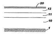
【0004】
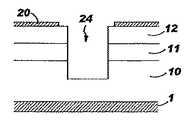
ILDに配線およびバイアを形成するための典型的なハードマスクを図1に概略的に示す。ILD10を(図示しない)下側のレベルを覆うバリア層1の上に配置する。ILDは、一般的には、有機ポリアリレンエーテル熱硬化性誘電体(organic polyarylene ether thermoset dielectric)もしくは同種の材料のようなポリマで形成される。ハードマスクは、3つの層11〜13を含む。永久ハードマスク層11は、低K材料(K<4.5)で形成される。このような材料の例としては、(Si,C,OおよびHを含有する)SiCOH,SiC,SiC:H,および(CおよびHを含有する)アモルファスSiのようなオルガノシリケート(organosilicate)が挙げられる。層11は、典型的には窒化シリコンである層12によって覆われ、層11と層12の厚さは、それぞれ約500Åと約350Åである。層13は、典型的には二酸化シリコンであり、約1500Åの厚さを有する。金属配線用パターンを層13へ転写し(“配線レベル(line-level)”・リソグラフィ)、図2に示されるようにマスク内に露出領域2を形成させる。さらなるプロセスは、図3に示されるように、レジストの層14を付着し、この層14をパターニングしてバイア開口部4を定める(“バイアレベル(via-level)”リソグラフィ)工程を含む。これは、層13をパターニングすることによって導入されたトポグラフィの上でレジスト14を少なくとも部分的に平坦化するということを必要とする。層13は、また、小平面の形成(すなわち、小平面3の形成)を免れず、これは限界寸法制御のロスを引き起こす。プラズマ・ポリマのその上への付着によって生じる配線縁部の粗化により、パターン転写の忠実度もまた低下する。
【0005】
さらに、図4に示されるように、後続のプロセスにおいて、エッチングされた配線とバイア開口部とを、(多くの場合ライナ15と共に)金属16で過充てんし、典型的には化学機械研磨(CMP)によって過剰な金属を除去する必要がある。金属16とライナ材料15とをほぼ同じ速度でCMPによって除去する場合(例えば、金属16が銅でありライナ15がタングステンである場合)には、残存するハードマスクは研磨停止層の機能も果たす必要がある。窒化シリコンの薄い層12は、CMP停止層として有効ではないであろう。
【0006】
【発明が解決しようとする課題】
ハードマスク構造が、低誘電率の利点を保持しながら極めて高い忠実度のパターン転写を備えるプロセスを可能にするとともに有効なCMP停止層を有する改良されたデュアル・ダマシン・プロセスの必要性が存在する。
【0007】
【課題を解決するための手段】
本発明は、上述した必要性を対象とするものであり、低K誘電体層の上側の酸化物層を少なくとも排除する犠牲ハードマスク層を含むハードマスク構造を用いるデュアル・ダマシン・プロセスを提供する。
【0008】
本発明の第一の態様によれば、3つのハードマスク層(下部層,中間層,上部層)を低K基板の上に付着する方法が提供される。上部ハードマスク層は、約200Åより薄い厚さを有する。第一のパターンに従って第一の開口部を上部ハードマスク層に形成し、それによって中間ハードマスク層の一部を露出させる。第二のパターンに従って第二の開口部を中間ハードマスク層の露出部分に形成し、対応する開口部を下部ハードマスク層に形成し、それによって基板の一部を露出させる。基板に開口部を形成し、そこに金属を付着する。過剰な金属をハードマスクの上に付着しその後除去してもよい。最後に、上部ハードマスク層を除去する。
【0009】
上部ハードマスク層の材料は、高融点金属,高融点金属ナイトライド,高融点金属合金,あるいは導電性Siベース材料(ドープトSiまたはドープトアモルファスSiのような)とすることができ、好ましくは、TaNのような高融点金属ナイトライドである。中間ハードマスク層は好ましくはSiNである。過剰な金属をCMPによって除去してもよく、上部ハードマスク層は研磨される際に過剰な金属より遅い研磨速度を有する。
【0010】
第一の開口部を形成するプロセスは、レジスト層を上部ハードマスク層の上に付着し、続いてそこからレジスト層を除去する工程を含んでもよく、中間ハードマスク層は、レジスト層の除去の際の酸化から下部ハードマスク層を保護するということを留意されたい。
【0011】
本発明の第二の態様によれば、下部ハードマスク層と上部ハードマスク層とを付着する方法が提供される。保護層を、下部ハードマスク層の上部表面と隣接する下部ハードマスク層の領域に形成する。この保護層は、レジスト除去が行われる際の酸化から下部ハードマスク層を保護する。上部表面領域に保護ナイトライド層を形成するかまたは、上部表面領域において下部ハードマスク層を高密度化するプラズマ処理に下部ハードマスク層をさらすことによって保護層を形成してもよい。保護層は約100Åの厚さを有する。
【0012】
本発明の他の態様によれば、下部ハードマスク層と上部ハードマスク層とを基板上に付着する方法が提供される。第一のパターンに従って第一の開口部を上部ハードマスク層に形成し、それによって下部ハードマスク層の一部を露出させる。このプロセスは、レジスト層を上部ハードマスク層の上に付着し、続いてそこからレジスト層を除去する工程を含む。レジスト層を非酸化レジスト・ストリップ・プロセスで除去し、下部ハードマスク層の酸化を回避する。特に、還元剤(reducing chemistry)を用いるプラズマ・レジスト・ストリップ・プロセスでレジストを除去してもよい。
【0013】
上部ハードマスク層はCMP停止層としても機能し得る薄い犠牲層であるということ、そして(一般的には低K材料から成る)下部ハードマスク層に対する酸化ダメージが回避されるということに注目されたい。
【0014】
【発明の実施の形態】
本発明のハードマスク構造は、低K誘電体ハードマスク層の上にあり、この層を保護する薄い(約100Å〜約200Å)犠牲層を用いる。この犠牲層は、金属配線パターンをエッチングするために有効なマスクであり、金属CMPプロセスにおいて有効な研磨停止層も提供する。
【0015】
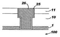
第一の実施の形態:3層ハードマスク
本実施の形態のハードマスクの構造を図5に示す。薄いハードマスク層20を、従来のハードマスクの酸化物層13の代わりに用いる(図1を対比されたい)。そして、薄いハードマスク層20は、3層ハードマスク構造の最上(上部)層である。下にある残留ハードマスクは、層11と層12とを含む。中間層12は、一般的には、典型的なプロセス工程(例えば、レジスト・マスクを用いるエッチング,レジスト・ストリップ(resist strip),湿式洗浄)の際に劣化しないという特性を有する誘電体材料から成る。この誘電体材料は、SiO2 ,SiN,SiON,SiOF,あるいは当業者に周知の同種の材料とすることができる。底部(下部)層11は、一般的には、SiC,SiC:H,オルガノシリケート(例えばSiCOH),SiCNH,スピンオンシルセスキオキサン(spin-on silsesquioxane),カーボンドープトオキシド(carbon-doped oxide),オルガノシリケートガラス,シリコンオキシカーバイド(silicon oxycarbide),アモルファス水素化シリコンカーバイド(amorphous hydrogenated silicon carbide),アモルファス水素化シリコンカーバイド/ナイトライド(amorphous hydrogenated silicon carbide/nitride),あるいは同種の適切な材料のような低誘電率材料から成る。この層は様々な典型的プロセス工程においてダメージを受け、したがって保護層(この場合には、誘電体層12)が必要とされるということが理解できる。特に、低K層11を、層20の付着の際およびレジスト・ストリップ・プロセスの際(例えばレジスト再構成の際)の酸化から保護する必要がある。
【0016】
層20は、少なくとも(i)層20の付着が下側の層にダメージを与えない、特に、層10および11の望ましい電気的性質を変質させない、および(ii)層20の研磨速度が、CMPによって除去される過剰な金属に比べて遅いという条件で、金属,金属化合物もしくは金属合金,半導体,または誘電体とすることができる。層20は、好ましくは高融点金属(例えばTa,Ti,W),高融点金属ナイトライド(例えばTaN,TiN,WN),高融点金属合金(例えばTaSiN,TiSiN,WSiN,TiW),導電性Siベース材料(ドープトSiまたはドープト・アモルファスSiのような),あるいは所定の他の金属(例えばCu,Al,Ag)である。より好ましくは、層20は高融点金属ナイトライドで形成される。特に、150ÅのTaN層が層10および11の望ましい性質を維持しながら良好なパターン忠実度をもたらすということが確認されている。
【0017】
この実施の形態において、ILD層10は、有機ポリアリレンエーテル熱硬化性誘電体で形成され、残留ハードマスク層11および12は、それぞれSiCおよびSiNである。そして、層20はTaNで形成される。層11および12は、化学蒸着法(CVD)によって形成されてもよく、またはプラズマCVDによって形成されてもよい。層11は、また、スピンオン・プロセスで付着されてもよい。層20は、物理蒸着法またはCVDによって形成されてもよい。
【0018】
図6〜12は、この実施の形態のハードマスクを用いるデュアル・ダマシン・プロセスにおける工程を説明する。レジスト層21をハードマスクの上に付着し、金属配線のパターンをそこに現像する。Cl2 またはCl2 /BCl3 化学物質(chemistry)を用いて層20に開口部22をエッチングすることにより、配線レベル・パターンをマスクへ転写する(図6)。次に、当業者に周知の方法を用いて、レジスト層21をストリップし、レジスト残留物を除去する。次に、第二のレジスト層23をマスクの上に付着し、バイア開口部24のパターンをそこに現像する(図7)。酸化物層13と比較して、層20は小平面の形成がはるかに少なく、導入されるトポグラフィがはるかに少ない(図3と図7を対比されたい)。
【0019】
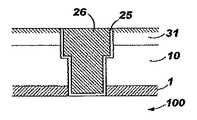
一続きのエッチング工程において、デュアル・ダマシン・パターンを残留ハードマスクへ最初に転写し、次にILDへ転写する。層11および12をフルオロカーボンベース化学物質を用いてエッチングする。次に、O2 ,O3 ,SO2 ,SO3 ,N2 ,NH3 ,N2 H2 ,N2 H4 ,H2 ,CO2 ,CO,CF4 ,CHF3 ,CH2 F2 またはCH3 Fのうちの1またはそれ以上を含む化学物質を用いて、ILD層10を部分的にエッチングする。このエッチングの際レジスト層23もまた除去する(図8)。次に、追加のフルオロカーボンベース・エッチングを、マスクとして層20を用いて実行し、金属配線パターンに従ってハードマスクの層11および12に開口部を形成する(開口部22)。さらなるエッチング工程は、先の部分的バイア・エッチングと同種の化学物質を用いて、配線レベル・パターンをILDに転写し、バイアの形成を完成させる(開口部24)。図9に示されるように、金属配線パターンを基板の上部に転写し、バイア・パターンを基板の下部に転写する。このエッチング工程は、バリア層1で停止し、バリア層1は典型的にはSiNまたはSiCで形成される。次に、フルオロカーボンベース・エッチングを用いてバリア層に開口部を形成し、その結果バイアのメタライゼーションが下のレベル100にコンタクトすることとなる。バイアの底部における開口部24の幅は、わずか約100nmとすることができる。
【0020】
メタライゼーション・プロセスは、好ましくはライナ25の付着と、それに続くバイア内,金属配線パターン内,そしてハードマスク上への金属26の付着とを含む(図10)。次に、CMPプロセスを用いて過剰な金属を研磨除去する。ライナ25のハードマスク層20の上にある部分も、一般的には、同一のCMPプロセスで除去する。特に、ライナ25がWであり金属26がCuである場合には、標準CMPプロセスは両者の間で選択的ではないであろう。このような場合、層20が研磨停止層として機能することが必要である(図11)。Cu用の典型的なCMPプロセスは、Wによって停止することはないが、Ti,Ta,TiN,またはTaNによって停止することとなる。したがって、この実施の形態で説明するTaNの層は、有効な研磨停止層を提供する。次に、層20を個別の研磨プロセスで除去する。この時点において、層12も除去して、ハードマスク構造のうちの低K層11だけが残留することが望ましい(図12)。
【0021】
この実施の形態のハードマスク構造は、図1のハードマスク構造と比べて限界寸法(金属配線の幅と間隔)制御の大いなる改善をもたらす。加えて、本実施の形態のハードマスクは、有効な研磨停止層を提供し、より信頼性の高いCMP金属除去プロセスの展開を可能にする。
【0022】
第二の実施の形態:2層ハードマスク
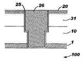
本実施の形態のハードマスクの構造を図13に示す。図5〜12と図13〜20との間で重複する参照符号は同一の構造を示す。第一の実施の形態におけるのと同様に、薄い犠牲ハードマスク層20がハードマスクの最上(上部)層を構成する。層20の材料は、高融点金属(例えばTa,Ti,W),高融点金属ナイトライド(例えばTaN,TiN,WN),高融点金属合金(例えばTaSiN,TiSiN,WSiN,TiW),導電性Siベース材料(ドープトSiまたはドープト・アモルファスSiのような),あるいは所定の他の金属(例えばCu,Al,Ag)とすることができる。好ましい材料はTaNであり、約150Åの厚さを有する。下側の層31は、第一の実施の形態の層11におけるのと同様にSiCOHまたは同種の材料のような低K誘電体であり、約500Åの厚さを有する。
【0023】
本実施の形態においては、(ナイトライド層12のような)中間ハードマスク層を排除する(図5と13を対比されたい)。これは、(i)低K層31を処理してこれをプロセスのダメージ(例えば、レジスト・ストリップ・プロセスの際の酸化によるダメージ)に強くする工程、および/または(ii)層31の露出した表面を酸化させないレジスト・ストリップ・プロセスを用いる工程によって成される。
【0024】
層31を、CVDまたはプラズマCVDを用いてILD層10の上に付着してもよい。この実施の形態においては、500Åの厚さのSiCOHをプラズマCVDによって付着する。次に、層31の表面を、層31の上部表面領域31t においてナイトライドを形成させるプラズマ(例えば、NH3 またはナイトライドベース・プラズマ)にさらす。代わりに、層31の表面を、表面領域31t において層を高密度化するプラズマ処理にさらしてもよく、あるいは層31を、領域31t において材料の密度が増加するという条件のもとで付着してもよい。上部表面領域31t は、約100Åの厚さを有する。
【0025】
他の方法においては、後段で詳述するような層31の表面を酸化させないレジスト・ストリップ・プロセスを用いることにより、低K層31のプラズマ処理または高密度化の必要性を回避できる。
【0026】
続いて、上部ハードマスク層20を層31の上に付着する。この実施の形態においては、150Åの厚さのTaNを物理蒸着法(PVD)によって付着する。上述したように、層20の付着プロセスが層31の性質を改質させず、層20の研磨速度が導電配線のために用いられる金属に比べて遅いという条件で、層20を、金属,半導体または誘電体とすることができる。
【0027】
図14〜20は、本実施の形態の2層ハードマスクを用いるデュアル・ダマシン・プロセスにおける工程を説明する図である。レジスト層21をハードマスクの上に付着する。次に、Cl2 またはCl2 /BCl3 化学物質を用いてハードマスク層20をパターニングして金属配線のパターンに従って開口部22を生じさせる配線レベル・パターニングを実行する(図14)。
【0028】
続いて、非酸化プラズマ・プロセス,還元プラズマ・プロセス,またはゆるい酸化プラズマ・プロセスを用いて、レジスト層21をストリップする。このプロセスは、好ましくは還元剤を用いるプラズマ・プロセスであり、最も好ましくは、層31の露出表面の酸化を防止するNH3 /H2 またはN2 /H2 プラズマ・プロセスである。代わりに、アセトンベース酸性(acetone-based acidic)レジスト・ストリップのような選択的溶媒ベース・レジスト・ストリップ・プロセスを用いてもよい。
【0029】
次に、レジスト層23を付着し、バイア開口部24のパターンをそこに現像するバイアレベル・パターニングを実行する(図15)。第一の実施の形態におけるのと同様に、配線レベル・パターンとバイアレベル・パターンとをハードマスク層31およびILD層10へ転写する。バイア・パターンをSiCOH層31へエッチングする。次に、バイア・パターンをILD層10へ転写する部分的バイア・エッチングを実行する(図16)。レジスト層23もこの部分的バイア・エッチング工程の際に除去する。次に、マスクとして層20を用いて追加のエッチングを実行し、金属配線パターンに従って層31に開口部を形成する(こうして、マスク層31内に開口部22を作成する)。図17に示されるように、先の部分的バイア・エッチングと同種の化学物質を用いるさらなるエッチング工程は、配線レベル・パターンをILDの上部へ転写し、ILDの下部を突き抜けるバイアの形成を完成する(開口部24)。
【0030】
次に、メタライゼーション・プロセス(好ましくは、ライナ25および金属26の付着を含む)を実行し、図18に示される構造を得る。次に、第一の実施の形態におけるのと同様に研磨停止層として機能する層20を用いるCMPプロセスを使用して、過剰な金属と露出したライナとを研磨除去する。過剰な金属を研磨した後(図19)、層20を個別の研磨プロセスで除去して図20に示される構造を得る。CMPによって層31の表面領域31t もまた除去することが望ましい。
【0031】
この実施の形態において、(層31から構成される)全残留ハードマスクが、ILD層10に加えて低K材料であるということに注目されたい。
【0032】
本実施の形態のハードマスクは、第一の実施の形態の利点を全て提供し、これに加えて、従来のハードマスク構造から1つの層を除くことにより、プロセスの複雑度の低減とプロセス時間の短縮化とを可能にする。
【0033】
特定の実施の形態の点から本発明を説明したが、多くの選択,変更および変形が当業者に対して明らかであることは、上述の説明にかんがみて明白である。したがって、本発明および特許請求の範囲の趣旨および範囲に含まれるこのような全ての選択,変更および変形を包含することを本発明は意図している。
【0034】
まとめとして、本発明の構成に関して以下の事項を開示する。
(1)金属パターンを基板に形成する方法であって、前記基板上に約4.5より低い誘電率を有する下部ハードマスク層を付着する工程と、前記下部ハードマスク層の上に中間ハードマスク層を付着する工程と、前記中間ハードマスク層の上に約200Åより薄い厚さを有する上部ハードマスク層を付着する工程と、第一のパターンに従って前記上部ハードマスク層に第一の開口部を形成し、それによって前記中間ハードマスク層の一部を露出させる工程と、第二のパターンに従って前記中間ハードマスク層の前記露出部分に第二の開口部を形成し、対応する開口部を前記下部ハードマスク層に形成し、それによって前記基板の一部を露出させる工程と、前記基板に開口部を形成する工程と、前記基板の開口部に金属を付着する工程と、前記上部ハードマスク層を除去する工程とを含む方法。
(2)前記上部ハードマスク層は、高融点金属,高融点金属ナイトライド,高融点金属合金,ドープトアモルファスシリコンおよびドープトシリコンより構成されるグループから選択された材料より成る上記(1)に記載の方法。
(3)前記中間ハードマスク層は、SiO2 ,SiN,SiONおよびSiOFより構成されるグループから選択された材料より成る上記(1)に記載の方法。(4)前記下部ハードマスク層は、SiC:H,SiCOH,SiCNH,カーボンドープトオキシド,オルガノシリケートガラス,シリコンオキシカーバイド,アモルファス水素化シリコンカーバイドおよびアモルファス水素化シリコンカーバイド/ナイトライドより構成されるグループから選択された材料より成る上記(1)に記載の方法。
(5)前記金属を付着する工程は、前記上部ハードマスク層の上に過剰な金属を付着する工程をさらに含み、前記上部ハードマスク層の研磨速度を前記金属の研磨速度より遅くして、化学機械研磨(CMP)プロセスで前記金属を研磨することによって前記過剰な金属を除去する工程をさらに含む上記(1)に記載の方法。
(6)前記第一の開口部を形成する工程は、前記上部ハードマスク層の上にレジスト層を付着し、続いて前記上部ハードマスク層から前記レジスト層を除去する工程を含み、前記中間ハードマスク層は前記レジスト層の除去の際の酸化から前記下部ハードマスク層を保護する上記(1)に記載の方法。
(7)約4より低い誘電率を有する基板に金属パターンを形成する方法であって、前記基板の上に約4.5より低い誘電率を有する下部ハードマスク層を付着する工程と、前記下部ハードマスク層の上部表面に隣接する下部ハードマスク層の領域に保護層を形成する工程と、前記下部ハードマスク層の上に約200Åより薄い厚さを有する上部ハードマスク層を付着する工程と、第一のパターンに従って前記上部ハードマスク層に第一の開口部を形成し、それによって前記下部ハードマスク層の一部を露出させる工程と、第二のパターンに従って前記下部ハードマスク層の前記露出部分に第二の開口部を形成し、それによって前記基板の一部を露出させる工程と、前記基板上に開口部を形成する工程と、前記基板の開口部に金属を付着する工程と、前記上部ハードマスク層を除去する工程とを含む方法。
(8)前記上部ハードマスク層の材料は、高融点金属,高融点金属ナイトライド,高融点金属合金,ドープトアモルファスシリコンおよびドープトシリコンより構成されるグループから選択される上記(7)に記載の方法。
(9)前記下部ハードマスク層は、SiC:H,SiCOH,SiCNH,カーボンドープトオキシド,オルガノシリケートガラス,シリコンオキシカーバイド,アモルファス水素化シリコンカーバイドおよびアモルファス水素化シリコンカーバイド/ナイトライドより構成されるグループから選択される材料より成る上記(7)に記載の方法。
(10)前記金属を付着する工程は、前記上部ハードマスク層の上に過剰な金属を付着する工程をさらに含み、前記上部ハードマスク層の研磨速度を前記金属の研磨速度より遅くして、化学機械研磨(CMP)プロセスで前記金属を研磨することによって前記過剰な金属を除去する工程をさらに含む上記(7)に記載の方法。
(11)前記第一の開口部を形成する工程は、前記上部ハードマスク層の上にレジスト層を付着し、続いて前記上部ハードマスク層から前記レジスト層を除去する工程を含み、前記保護層を形成する工程は、前記下部ハードマスク層をプラズマにさらし、それによって前記領域に、前記レジスト層の除去の際の酸化から前記下部ハードマスク層を保護する保護ナイトライド層を形成する工程を含む上記(7)に記載の方法。
(12)前記第一の開口部を形成する工程は、前記上部ハードマスク層の上にレジスト層を付着し、続いて前記上部ハードマスク層から前記レジスト層を除去する工程を含み、前記保護層を形成する工程は、前記領域において前記下部ハードマスク層を高密度化するプラズマに前記下部ハードマスク層をさらす工程を含み、前記保護層が前記レジスト層の除去の際の酸化から前記下部ハードマスク層を保護する上記(7)に記載の方法。
(13)前記下部ハードマスク層の上部表面に隣接する領域において前記下部ハードマスク層の材料の密度が増加するという条件のもとで前記下部ハードマスク層を付着する上記(7)に記載の方法。
(14)前記第一の開口部を形成する工程は、前記上部ハードマスク層の上にレジスト層を付着し、続いて前記上部ハードマスク層から前記レジスト層を除去する工程を含み、前記レジスト層は非酸化レジスト・ストリップ・プロセスで除去される上記(7)に記載の方法。
(15)前記保護層は約100Åの厚さを有する上記(7)に記載の方法。
(16)約4より低い誘電率を有する基板に金属パターンを形成する方法であって、前記基板上に約4.5より低い誘電率を有する下部ハードマスク層を付着する工程と、前記下部ハードマスク層の上に約200Åより薄い厚さを有する上部ハードマスク層を付着する工程と、第一のパターンに従って前記上部ハードマスク層に第一の開口部を形成し、それによって前記下部ハードマスク層の一部を露出させる工程と、第二のパターンに従って前記下部ハードマスク層の前記露出部分に第二の開口部を形成し、それによって前記基板の一部を露出させる工程と、前記基板に開口部を形成する工程と、前記基板の開口部に金属を付着する工程と、前記上部ハードマスク層を除去する工程とを含み、前記第一の開口部を形成する工程は、前記上部ハードマスク層の上にレジスト層を付着し、続いて前記上部ハードマスク層から前記レジスト層を除去する工程をさらに含み、前記レジスト層は非酸化レジスト・ストリップ・プロセスで除去される方法。
(17)前記上部ハードマスク層の材料は、高融点金属,高融点金属ナイトライド,高融点金属合金,ドープトアモルファスシリコンおよびドープトシリコンより構成されるグループから選択される上記(16)に記載の方法。
(18)前記下部ハードマスク層は、SiC:H,SiCOH,SiCNH,カーボンドープトオキシド,オルガノシリケートガラス,シリコンオキシカーバイド,アモルファス水素化シリコンカーバイドおよびアモルファス水素化シリコンカーバイド/ナイトライドより構成されるグループから選択される材料より成る上記(16)に記載の方法。
(19)前記金属を付着する工程は、前記上部ハードマスク層の上に過剰な金属を付着する工程をさらに含み、前記上部ハードマスク層の研磨速度を前記金属の研磨速度より遅くして、化学機械研磨(CMP)プロセスで前記金属を研磨することによって前記過剰な金属を除去する工程をさらに含む上記(16)に記載の方法。
(20)前記レジスト・ストリップ・プロセスは、還元剤を用いるプラズマ・プロセスである上記(16)に記載の方法。
【図面の簡単な説明】
【図1】デュアル・ダマシン・プロセスにおいて用いられる典型的なハードマスク構造の概略図である。
【図2】図1のハードマスクを用いる際に直面するプロセスの問題のいくつかを説明する図である。
【図3】図1のハードマスクを用いる際に直面するプロセスの問題のいくつかを説明する図である。
【図4】図1のハードマスクを用いる際に直面するプロセスの問題のいくつかを説明する図である。
【図5】本発明の第一の実施の形態に従って、3層ハードマスクを用いるデュアル・ダマシン・プロセスを説明する図である。
【図6】本発明の第一の実施の形態に従って、3層ハードマスクを用いるデュアル・ダマシン・プロセスを説明する図である。
【図7】本発明の第一の実施の形態に従って、3層ハードマスクを用いるデュアル・ダマシン・プロセスを説明する図である。
【図8】本発明の第一の実施の形態に従って、3層ハードマスクを用いるデュアル・ダマシン・プロセスを説明する図である。
【図9】本発明の第一の実施の形態に従って、3層ハードマスクを用いるデュアル・ダマシン・プロセスを説明する図である。
【図10】本発明の第一の実施の形態に従って、3層ハードマスクを用いるデュアル・ダマシン・プロセスを説明する図である。
【図11】本発明の第一の実施の形態に従って、3層ハードマスクを用いるデュアル・ダマシン・プロセスを説明する図である。
【図12】本発明の第一の実施の形態に従って、3層ハードマスクを用いるデュアル・ダマシン・プロセスを説明する図である。
【図13】本発明の第二の実施の形態に従って、2層ハードマスクを用いるデュアル・ダマシン・プロセスを説明する図である。
【図14】本発明の第二の実施の形態に従って、2層ハードマスクを用いるデュアル・ダマシン・プロセスを説明する図である。
【図15】本発明の第二の実施の形態に従って、2層ハードマスクを用いるデュアル・ダマシン・プロセスを説明する図である。
【図16】本発明の第二の実施の形態に従って、2層ハードマスクを用いるデュアル・ダマシン・プロセスを説明する図である。
【図17】本発明の第二の実施の形態に従って、2層ハードマスクを用いるデュアル・ダマシン・プロセスを説明する図である。
【図18】本発明の第二の実施の形態に従って、2層ハードマスクを用いるデュアル・ダマシン・プロセスを説明する図である。
【図19】本発明の第二の実施の形態に従って、2層ハードマスクを用いるデュアル・ダマシン・プロセスを説明する図である。
【図20】本発明の第二の実施の形態に従って、2層ハードマスクを用いるデュアル・ダマシン・プロセスを説明する図である。
【符号の説明】
1 バリア層
2 露出領域
3 小平面
4 バイア開口部
10 ILD層
11 ハードマスク層
12 ハードマスク層
13 ハードマスク層
14 レジスト層
15 ライナ
16 金属
20 ハードマスク層
21 レジスト層
22 開口部
23 第二のレジスト層
24 バイア開口部
25 ライナ
26 金属
31 ハードマスク層
31t 上部表面領域
100 レベル[0001]
BACKGROUND OF THE INVENTION
The present invention relates to semiconductor processes, and more particularly to critical dimension control in deep sub-micron lithography for wiring fabrication in a dual damascene process.
[0002]
This application is related to US patent application Ser. No. 09 / 550,943 filed Apr. 17, 2000 and assigned to the same assignee as the present application and referred to as “Protective Hard Mask for Fabricating Wiring Structure”. . The disclosure of this related application is cited as the content of the specification.
[0003]
[Prior art]
Devices with multilayer wiring structures are well known in the semiconductor industry. The dual damascene process has proven to be a successful method for producing such structures. This process generally includes the steps of embedding metal interconnects in an interlevel dielectric (ILD) layer and connecting the metal layers by metallizing via holes formed in the ILD. Including. In order to improve the overall device electrical performance, it is highly desirable that the ILD have a low dielectric constant (K <4). In addition, in very fine pitch (<300 nm) devices, wiring and via holes must be etched into the ILD with critical dimensions of about 100 nm. This generally requires etching using a hard mask. In addition, it is often desirable to avoid a mask removal process where a portion of the hard mask remaining on the ILD can damage the ILD. This layer is sometimes referred to as a “residual hardmask” or “permanent hardmask”. Therefore, the hard mask layer in contact with the low K ILD also needs to have a low dielectric constant.
[0004]
A typical hard mask for forming interconnects and vias in the ILD is schematically illustrated in FIG. An ILD 10 is placed on the
[0005]
Further, as shown in FIG. 4, in subsequent processes, the etched wiring and via openings are overfilled with metal 16 (often along with liner 15), typically chemical mechanical polishing (CMP). ) To remove excess metal. When the
[0006]
[Problems to be solved by the invention]
There is a need for an improved dual damascene process that enables a process with very high fidelity pattern transfer while the hard mask structure retains the advantages of low dielectric constant and has an effective CMP stop layer .
[0007]
[Means for Solving the Problems]
The present invention addresses the aforementioned needs and provides a dual damascene process using a hard mask structure that includes a sacrificial hard mask layer that at least eliminates the oxide layer above the low-K dielectric layer. .
[0008]
According to a first aspect of the present invention, a method is provided for depositing three hard mask layers (lower layer, intermediate layer, upper layer) on a low K substrate. The upper hard mask layer has a thickness less than about 200 mm. A first opening is formed in the upper hard mask layer according to the first pattern, thereby exposing a portion of the intermediate hard mask layer. A second opening is formed in the exposed portion of the intermediate hard mask layer according to the second pattern, and a corresponding opening is formed in the lower hard mask layer, thereby exposing a portion of the substrate. An opening is formed in the substrate, and metal is attached thereto. Excess metal may be deposited on the hard mask and then removed. Finally, the upper hard mask layer is removed.
[0009]
The material of the upper hard mask layer can be a refractory metal, a refractory metal nitride, a refractory metal alloy, or a conductive Si base material (such as doped Si or doped amorphous Si), preferably It is a refractory metal nitride such as TaN. The intermediate hard mask layer is preferably SiN. Excess metal may be removed by CMP, and the upper hard mask layer has a slower polishing rate than the excess metal when polished.
[0010]
The process of forming the first opening may include the steps of depositing a resist layer over the upper hard mask layer and subsequently removing the resist layer therefrom, the intermediate hard mask layer being a resist layer removal layer. Note that the lower hard mask layer is protected from oxidation during the process.
[0011]
According to a second aspect of the present invention, a method for depositing a lower hard mask layer and an upper hard mask layer is provided. A protective layer is formed in the region of the lower hard mask layer adjacent to the upper surface of the lower hard mask layer. This protective layer protects the lower hard mask layer from oxidation during resist removal. A protective nitride layer may be formed in the upper surface region, or the protective layer may be formed by exposing the lower hard mask layer to a plasma treatment that densifies the lower hard mask layer in the upper surface region. The protective layer has a thickness of about 100 mm.
[0012]
According to another aspect of the invention, a method is provided for depositing a lower hard mask layer and an upper hard mask layer on a substrate. A first opening is formed in the upper hard mask layer according to the first pattern, thereby exposing a portion of the lower hard mask layer. The process includes depositing a resist layer over the top hard mask layer and subsequently removing the resist layer therefrom. The resist layer is removed with a non-oxidized resist strip process to avoid oxidation of the lower hard mask layer. In particular, the resist may be removed by a plasma resist strip process using reducing chemistry.
[0013]
Note that the upper hard mask layer is a thin sacrificial layer that can also function as a CMP stop layer, and that oxidative damage to the lower hard mask layer (typically of a low K material) is avoided. .
[0014]
DETAILED DESCRIPTION OF THE INVENTION
The hard mask structure of the present invention uses a thin (about 100 to about 200) sacrificial layer overlying and protecting the low-K dielectric hard mask layer. This sacrificial layer is an effective mask for etching the metal wiring pattern, and also provides a polishing stop layer effective in the metal CMP process.
[0015]
First embodiment: three-layer hard mask
The structure of the hard mask of this embodiment is shown in FIG. A thin
[0016]
[0017]
In this embodiment, the
[0018]
6-12 illustrate the steps in a dual damascene process using the hard mask of this embodiment. A resist
[0019]
In a series of etching steps, the dual damascene pattern is first transferred to the residual hard mask and then transferred to the ILD.
[0020]
The metallization process preferably includes deposition of
[0021]
The hard mask structure of this embodiment provides a significant improvement in the control of critical dimensions (metal wiring width and spacing) compared to the hard mask structure of FIG. In addition, the hard mask of the present embodiment provides an effective polishing stop layer and enables the development of a more reliable CMP metal removal process.
[0022]
Second embodiment: two-layer hard mask
The structure of the hard mask of this embodiment mode is shown in FIG. Reference numerals overlapping between FIGS. 5 to 12 and FIGS. 13 to 20 indicate the same structure. As in the first embodiment, the thin sacrificial
[0023]
In the present embodiment, an intermediate hard mask layer (such as nitride layer 12) is eliminated (compare FIGS. 5 and 13). This may include (i) treating the
[0024]
[0025]
In other methods, the need for plasma treatment or densification of the
[0026]
Subsequently, an upper
[0027]
FIGS. 14 to 20 are diagrams illustrating steps in the dual damascene process using the two-layer hard mask of the present embodiment. A resist
[0028]
Subsequently, the resist
[0029]
Next, via-level patterning is performed to deposit a resist
[0030]
Next, a metallization process (preferably involving deposition of
[0031]
Note that in this embodiment, the total residual hard mask (consisting of layer 31) is a low-K material in addition to the
[0032]
The hard mask of this embodiment provides all of the advantages of the first embodiment, and in addition to this, by removing one layer from the conventional hard mask structure, the process complexity is reduced and the process time is reduced. Can be shortened.
[0033]
Although the present invention has been described in terms of particular embodiments, it will be apparent in view of the foregoing description that many choices, modifications and variations will be apparent to those skilled in the art. Accordingly, the present invention is intended to embrace all such alternatives, modifications and variations that fall within the spirit and scope of the present invention and claims.
[0034]
In summary, the following matters are disclosed regarding the configuration of the present invention.
(1) A method of forming a metal pattern on a substrate, comprising depositing a lower hard mask layer having a dielectric constant lower than about 4.5 on the substrate, and an intermediate hard mask on the lower hard mask layer. Depositing a layer, depositing an upper hard mask layer having a thickness of less than about 200 mm on the intermediate hard mask layer, and forming a first opening in the upper hard mask layer according to a first pattern. Forming a second opening in the exposed portion of the intermediate hard mask layer according to a second pattern, and exposing a portion of the intermediate hard mask layer in accordance with a second pattern; Forming a hard mask layer thereby exposing a portion of the substrate; forming an opening in the substrate; attaching a metal to the opening in the substrate; Method comprising the step of removing the part hard mask layer.
(2) In the above (1), the upper hard mask layer is made of a material selected from the group consisting of a refractory metal, a refractory metal nitride, a refractory metal alloy, doped amorphous silicon, and doped silicon. The method described.
(3) The intermediate hard mask layer is made of SiO.2 The method according to (1) above, comprising a material selected from the group consisting of SiN, SiON, and SiOF. (4) The lower hard mask layer is made of SiC: H, SiCOH, SiCNH, carbon doped oxide, organosilicate glass, silicon oxycarbide, amorphous hydrogenated silicon carbide, and amorphous hydrogenated silicon carbide / nitride. The method according to (1) above, comprising a material selected from:
(5) The step of depositing the metal further includes the step of depositing excess metal on the upper hard mask layer, and the polishing rate of the upper hard mask layer is made slower than the polishing rate of the metal, The method according to (1), further comprising removing the excess metal by polishing the metal in a mechanical polishing (CMP) process.
(6) The step of forming the first opening includes a step of attaching a resist layer on the upper hard mask layer, and subsequently removing the resist layer from the upper hard mask layer. The method according to (1) above, wherein the mask layer protects the lower hard mask layer from oxidation during the removal of the resist layer.
(7) A method of forming a metal pattern on a substrate having a dielectric constant lower than about 4, comprising depositing a lower hard mask layer having a dielectric constant lower than about 4.5 on the substrate; Forming a protective layer in a region of the lower hard mask layer adjacent to the upper surface of the hard mask layer; depositing an upper hard mask layer having a thickness of less than about 200 mm on the lower hard mask layer; Forming a first opening in the upper hard mask layer according to a first pattern, thereby exposing a portion of the lower hard mask layer; and exposing the portion of the lower hard mask layer according to a second pattern Forming a second opening, thereby exposing a portion of the substrate, forming an opening on the substrate, and attaching a metal to the opening of the substrate. If the method comprising the step of removing the upper hard mask layer.
(8) The material of the upper hard mask layer is described in (7) above, which is selected from the group consisting of a refractory metal, a refractory metal nitride, a refractory metal alloy, doped amorphous silicon, and doped silicon. the method of.
(9) The lower hard mask layer is made of SiC: H, SiCOH, SiCNH, carbon doped oxide, organosilicate glass, silicon oxycarbide, amorphous hydrogenated silicon carbide, and amorphous hydrogenated silicon carbide / nitride. The method according to (7) above, comprising a material selected from:
(10) The step of depositing the metal further includes the step of depositing excess metal on the upper hard mask layer, and the polishing rate of the upper hard mask layer is made slower than the polishing rate of the metal, The method according to (7), further comprising removing the excess metal by polishing the metal by a mechanical polishing (CMP) process.
(11) The step of forming the first opening includes a step of depositing a resist layer on the upper hard mask layer, and subsequently removing the resist layer from the upper hard mask layer. Forming a protective nitride layer that exposes the lower hard mask layer to plasma, thereby protecting the lower hard mask layer from oxidation during removal of the resist layer in the region. The method according to (7) above.
(12) The step of forming the first opening includes a step of attaching a resist layer on the upper hard mask layer, and subsequently removing the resist layer from the upper hard mask layer, Forming a step of exposing the lower hard mask layer to a plasma that densifies the lower hard mask layer in the region, wherein the protective layer removes the lower hard mask from oxidation during removal of the resist layer. The method according to (7) above, wherein the layer is protected.
(13) The method according to (7), wherein the lower hard mask layer is deposited under a condition that a material density of the lower hard mask layer increases in a region adjacent to the upper surface of the lower hard mask layer. .
(14) The step of forming the first opening includes a step of attaching a resist layer on the upper hard mask layer, and subsequently removing the resist layer from the upper hard mask layer. The method of (7) above, wherein is removed by a non-oxidized resist strip process.
(15) The method according to (7), wherein the protective layer has a thickness of about 100 mm.
(16) A method of forming a metal pattern on a substrate having a dielectric constant lower than about 4, comprising depositing a lower hard mask layer having a dielectric constant lower than about 4.5 on the substrate; Depositing an upper hard mask layer having a thickness of less than about 200 mm on the mask layer, and forming a first opening in the upper hard mask layer according to a first pattern, thereby forming the lower hard mask layer; Exposing a portion of the substrate, forming a second opening in the exposed portion of the lower hard mask layer according to a second pattern, thereby exposing a portion of the substrate, and opening the substrate Forming the first opening, and forming the first opening includes the steps of forming a portion, attaching a metal to the opening of the substrate, and removing the upper hard mask layer. The resist layer deposited on the Domasuku layer, followed by further comprising the step of removing the resist layer from the upper hard mask layer, the resist layer is a method that is removed in a non-oxidizing resist strip process.
(17) The material of the upper hard mask layer is described in (16) above, which is selected from the group consisting of a refractory metal, a refractory metal nitride, a refractory metal alloy, doped amorphous silicon, and doped silicon. the method of.
(18) The lower hard mask layer is made of SiC: H, SiCOH, SiCNH, carbon doped oxide, organosilicate glass, silicon oxycarbide, amorphous hydrogenated silicon carbide, and amorphous hydrogenated silicon carbide / nitride. The method according to (16), comprising a material selected from:
(19) The step of depositing the metal further includes the step of depositing excess metal on the upper hard mask layer, and the polishing rate of the upper hard mask layer is made slower than the polishing rate of the metal, The method according to (16), further comprising removing the excess metal by polishing the metal in a mechanical polishing (CMP) process.
(20) The method according to (16), wherein the resist strip process is a plasma process using a reducing agent.
[Brief description of the drawings]
FIG. 1 is a schematic diagram of an exemplary hard mask structure used in a dual damascene process.
FIG. 2 illustrates some of the process problems encountered when using the hard mask of FIG.
FIG. 3 illustrates some of the process problems encountered when using the hard mask of FIG.
FIG. 4 illustrates some of the process problems encountered when using the hard mask of FIG.
FIG. 5 illustrates a dual damascene process using a three-layer hard mask according to the first embodiment of the present invention.
FIG. 6 illustrates a dual damascene process using a three-layer hard mask in accordance with the first embodiment of the present invention.
FIG. 7 illustrates a dual damascene process using a three-layer hard mask according to the first embodiment of the present invention.
FIG. 8 illustrates a dual damascene process using a three-layer hard mask according to the first embodiment of the present invention.
FIG. 9 illustrates a dual damascene process using a three-layer hard mask according to the first embodiment of the present invention.
FIG. 10 illustrates a dual damascene process using a three-layer hard mask in accordance with the first embodiment of the present invention.
FIG. 11 illustrates a dual damascene process using a three-layer hard mask according to the first embodiment of the present invention.
FIG. 12 illustrates a dual damascene process using a three-layer hard mask according to the first embodiment of the present invention.
FIG. 13 illustrates a dual damascene process using a two-layer hard mask according to a second embodiment of the present invention.
FIG. 14 is a diagram illustrating a dual damascene process using a two-layer hard mask according to a second embodiment of the present invention.
FIG. 15 illustrates a dual damascene process using a two-layer hard mask according to a second embodiment of the present invention.
FIG. 16 illustrates a dual damascene process using a two-layer hard mask according to a second embodiment of the present invention.
FIG. 17 illustrates a dual damascene process using a two-layer hard mask in accordance with a second embodiment of the present invention.
FIG. 18 illustrates a dual damascene process using a two-layer hard mask in accordance with a second embodiment of the present invention.
FIG. 19 illustrates a dual damascene process using a two-layer hard mask in accordance with a second embodiment of the present invention.
FIG. 20 is a diagram illustrating a dual damascene process using a two-layer hard mask in accordance with a second embodiment of the present invention.
[Explanation of symbols]
1 Barrier layer
2 Exposed area
3 Small plane
4 Via opening
10 ILD layer
11 Hard mask layer
12 Hard mask layer
13 Hard mask layer
14 resist layer
15 liner
16 metal
20 Hard mask layer
21 resist layer
22 opening
23 Second resist layer
24 Bia opening
25 liner
26 metal
31 Hard mask layer
31t Upper surface area
100 levels
Claims (20)
Translated fromJapanese前記基板上に4.5より低い誘電率を有する下部ハードマスク層を付着する工程と、
前記下部ハードマスク層の上に中間ハードマスク層を付着する工程と、
前記中間ハードマスク層の上に200Åより薄い厚さを有する上部ハードマスク層を付着する工程と、
第一のパターンに従って前記上部ハードマスク層に第一の開口部を形成し、それによって前記中間ハードマスク層の一部を露出させる工程と、
第二のパターンに従って前記中間ハードマスク層の前記露出部分に第二の開口部を形成し、対応する開口部を前記下部ハードマスク層に形成し、それによって前記基板の一部を露出させる工程と、
前記露出した基板を部分的にエッチングする工程と、
前記上部ハードマスク層をマスクとして、中間ハードマスク層および下部ハードマスク層に開口部を形成する工程と、
前記基板の上部には第一のパターンに対応した溝部を、下部には第二のパターンに対応した開口部を形成する工程と、
前記基板の開口部に金属を付着する工程と、
前記上部ハードマスク層を除去する工程とを含み、
前記金属を付着する工程は、前記上部ハードマスク層の上に過剰な金属を付着する工程をさらに含み、
前記上部ハードマスク層の研磨速度を前記金属の研磨速度より遅くして、化学機械研磨(CMP)プロセスで前記金属を研磨することによって前記過剰な金属を除去する工程をさらに含み、
前記上部ハードマスク層は、高融点金属,高融点金属ナイトライド,高融点金属合金,ドープトアモルファスシリコンおよびドープトシリコンより構成されるグループから選択された材料より成る方法。A method of forming a metal pattern on a substrate having a dielectric constant less than 4, comprising:
Depositing a lower hard mask layer having a dielectric constant lower than 4.5 on the substrate;
Depositing an intermediate hard mask layer on the lower hard mask layer;
Depositing an upper hard mask layer having a thickness of less than 200 mm on the intermediate hard mask layer;
Forming a first opening in the upper hard mask layer according to a first pattern, thereby exposing a portion of the intermediate hard mask layer;
Forming a second opening in the exposed portion of the intermediate hard mask layer according to a second pattern, forming a corresponding opening in the lower hard mask layer, thereby exposing a portion of the substrate; ,
Partially etching the exposed substrate;
Using the upper hard mask layer as a mask, forming an opening in the intermediate hard mask layer and the lower hard mask layer;
Forminga groove corresponding to the first pattern in the upper portion of the substrate and forming an openingcorresponding to the second pattern in the lower portion ;
Attaching metal to the opening of the substrate;
Removing the upper hard mask layer,
Depositing the metal further comprises depositing excess metal over the upper hardmask layer;
Further comprising removing the excess metal by polishing the metal in a chemical mechanical polishing (CMP) process with a polishing rate of the upper hard mask layer slower than the polishing rate of the metal.
The upper hard mask layer is made of a material selected from the group consisting of a refractory metal, a refractory metal nitride, a refractory metal alloy, doped amorphous silicon, and doped silicon.
前記中間ハードマスク層は前記レジスト層の除去の際の酸化から前記下部ハードマスク層を保護する請求項1〜3いずれか1つに記載の方法。Forming the first opening includes depositing a resist layer on the upper hard mask layer and subsequently removing the resist layer from the upper hard mask layer;
The method of claim 1, wherein the intermediate hard mask layer protects the lower hard mask layer from oxidation during removal of the resist layer.
前記基板の上に4.5より低い誘電率を有する下部ハードマスク層を付着する工程と、
前記下部ハードマスク層の上部表面に隣接する下部ハードマスク層の領域に保護層を形成する工程と、
前記下部ハードマスク層の上に200Åより薄い厚さを有する上部ハードマスク層を付着する工程と、
第一のパターンに従って前記上部ハードマスク層に第一の開口部を形成し、それによって前記下部ハードマスク層の一部を露出させる工程と、
第二のパターンに従って前記下部ハードマスク層の前記露出部分に第二の開口部を形成し、それによって前記基板の一部を露出させる工程と、
前記露出した基板を部分的にエッチングする工程と、
前記上部ハードマスク層をマスクとして、保護層および下部ハードマスク層に開口部を形成する工程と、
前記基板の上部には第一のパターンに対応した溝部を、下部には第二のパターンに対応した開口部を形成する工程と、
前記基板の開口部に金属を付着する工程と、
前記上部ハードマスク層を除去する工程とを含み、
前記金属を付着する工程は、前記上部ハードマスク層の上に過剰な金属を付着する工程をさらに含み、
前記上部ハードマスク層の研磨速度を前記金属の研磨速度より遅くして、化学機械研磨(CMP)プロセスで前記金属を研磨することによって前記過剰な金属を除去する工程をさらに含み、
前記上部ハードマスク層の材料は、高融点金属,高融点金属ナイトライド,高融点金属合金,ドープトアモルファスシリコンおよびドープトシリコンより構成されるグループから選択される方法。A method of forming a metal pattern on a substrate having a dielectric constant lower than 4, comprising:
Depositing a lower hard mask layer having a dielectric constant lower than 4.5 on the substrate;
Forming a protective layer in a region of the lower hard mask layer adjacent to the upper surface of the lower hard mask layer;
Depositing an upper hard mask layer having a thickness of less than 200 mm on the lower hard mask layer;
Forming a first opening in the upper hard mask layer according to a first pattern, thereby exposing a portion of the lower hard mask layer;
Forming a second opening in the exposed portion of the lower hard mask layer according to a second pattern, thereby exposing a portion of the substrate;
Partially etching the exposed substrate;
Using the upper hard mask layer as a mask, forming an opening in theprotective layer and the lower hard mask layer;
Forminga groove corresponding to the first pattern in the upper portion of the substrate and forming an openingcorresponding to the second pattern in the lower portion ;
Attaching metal to the opening of the substrate;
Removing the upper hard mask layer,
Depositing the metal further comprises depositing excess metal over the upper hardmask layer;
Further comprising removing the excess metal by polishing the metal in a chemical mechanical polishing (CMP) process with a polishing rate of the upper hard mask layer slower than the polishing rate of the metal.
The material of the upper hard mask layer is selected from the group consisting of a refractory metal, a refractory metal nitride, a refractory metal alloy, doped amorphous silicon, and doped silicon.
前記保護層を形成する工程は、前記下部ハードマスク層をプラズマにさらし、それによって前記領域に、前記レジスト層の除去の際の酸化から前記下部ハードマスク層を保護する保護ナイトライド層を形成する工程を含む請求項7または8に記載の方法。Forming the first opening includes depositing a resist layer on the upper hard mask layer and subsequently removing the resist layer from the upper hard mask layer;
The step of forming the protective layer includes exposing the lower hard mask layer to plasma, thereby forming a protective nitride layer in the region to protect the lower hard mask layer from oxidation during the removal of the resist layer. The method according to claim 7 or 8, comprising a step.
前記保護層を形成する工程は、前記領域において前記下部ハードマスク層を高密度化するプラズマに前記下部ハードマスク層をさらす工程を含み、
前記保護層が前記レジスト層の除去の際の酸化から前記下部ハードマスク層を保護する請求項7〜9いずれか1つに記載の方法。Forming the first opening includes depositing a resist layer on the upper hard mask layer and subsequently removing the resist layer from the upper hard mask layer;
Forming the protective layer includes exposing the lower hard mask layer to plasma that densifies the lower hard mask layer in the region;
The method according to claim 7, wherein the protective layer protects the lower hard mask layer from oxidation during the removal of the resist layer.
前記レジスト層は非酸化レジスト・ストリップ・プロセスで除去される請求項7〜11いずれか1つに記載の方法。Forming the first opening includes depositing a resist layer on the upper hard mask layer and subsequently removing the resist layer from the upper hard mask layer;
The method of any one of claims 7-11, wherein the resist layer is removed by a non-oxidized resist strip process.
前記基板上に4.5より低い誘電率を有する下部ハードマスク層を付着する工程と、
前記下部ハードマスク層の上に200Åより薄い厚さを有する上部ハードマスク層を付着する工程と、
第一のパターンに従って前記上部ハードマスク層に第一の開口部を形成し、それによって前記下部ハードマスク層の一部を露出させる工程と、
第二のパターンに従って前記下部ハードマスク層の前記露出部分に第二の開口部を形成し、それによって前記基板の一部を露出させる工程と、
前記露出した基板を部分的にエッチングする工程と、
前記上部ハードマスク層をマスクとして、下部ハードマスク層に開口部を形成する工程と、
前記基板の上部には第一のパターンに対応した溝部を、下部には第二のパターンに対応した開口部を形成する工程と、
前記基板の開口部に金属を付着する工程と、
前記上部ハードマスク層を除去する工程とを含み、
前記第一の開口部を形成する工程は、前記上部ハードマスク層の上にレジスト層を付着し、続いて前記上部ハードマスク層から前記レジスト層を除去する工程をさらに含み、
前記レジスト層は非酸化レジスト・ストリップ・プロセスで除去され、
前記金属を付着する工程は、前記上部ハードマスク層の上に過剰な金属を付着する工程をさらに含み、
前記上部ハードマスク層の研磨速度を前記金属の研磨速度より遅くして、化学機械研磨(CMP)プロセスで前記金属を研磨することによって前記過剰な金属を除去する工程をさらに含み、
前記上部ハードマスク層の材料は、高融点金属,高融点金属ナイトライド,高融点金属合金,ドープトアモルファスシリコンおよびドープトシリコンより構成されるグループから選択される方法。A method of forming a metal pattern on a substrate having a dielectric constant lower than 4, comprising:
Depositing a lower hard mask layer having a dielectric constant lower than 4.5 on the substrate;
Depositing an upper hard mask layer having a thickness of less than 200 mm on the lower hard mask layer;
Forming a first opening in the upper hard mask layer according to a first pattern, thereby exposing a portion of the lower hard mask layer;
Forming a second opening in the exposed portion of the lower hard mask layer according to a second pattern, thereby exposing a portion of the substrate;
Partially etching the exposed substrate;
As a mask the upper hard masklayer, forming an opening at thebottom hard mask layer,
Forminga groove corresponding to the first pattern in the upper portion of the substrate and forming an openingcorresponding to the second pattern in the lower portion ;
Attaching metal to the opening of the substrate;
Removing the upper hard mask layer,
Forming the first opening further includes depositing a resist layer on the upper hard mask layer and subsequently removing the resist layer from the upper hard mask layer;
The resist layer is removed by a non-oxidized resist strip process;
Depositing the metal further comprises depositing excess metal over the upper hardmask layer;
Further comprising removing the excess metal by polishing the metal in a chemical mechanical polishing (CMP) process with a polishing rate of the upper hard mask layer slower than the polishing rate of the metal.
The material of the upper hard mask layer is selected from the group consisting of a refractory metal, a refractory metal nitride, a refractory metal alloy, doped amorphous silicon, and doped silicon.
Applications Claiming Priority (2)
| Application Number | Priority Date | Filing Date | Title |
|---|---|---|---|
| US10/053,288US6734096B2 (en) | 2002-01-17 | 2002-01-17 | Fine-pitch device lithography using a sacrificial hardmask |
| US10/053288 | 2002-01-17 |
Publications (2)
| Publication Number | Publication Date |
|---|---|
| JP2003218109A JP2003218109A (en) | 2003-07-31 |
| JP4169150B2true JP4169150B2 (en) | 2008-10-22 |
Family
ID=21983171
Family Applications (1)
| Application Number | Title | Priority Date | Filing Date |
|---|---|---|---|
| JP2003003569AExpired - Fee RelatedJP4169150B2 (en) | 2002-01-17 | 2003-01-09 | Method of forming a metal pattern using a sacrificial hard mask |
Country Status (2)
| Country | Link |
|---|---|
| US (1) | US6734096B2 (en) |
| JP (1) | JP4169150B2 (en) |
Families Citing this family (33)
| Publication number | Priority date | Publication date | Assignee | Title |
|---|---|---|---|---|
| US6740579B2 (en)* | 2002-06-18 | 2004-05-25 | Intel Corporation | Method of making a semiconductor device that includes a dual damascene interconnect |
| US6930048B1 (en)* | 2002-09-18 | 2005-08-16 | Lam Research Corporation | Etching a metal hard mask for an integrated circuit structure |
| US6969685B1 (en)* | 2002-09-18 | 2005-11-29 | Lam Research Corporation | Etching a dielectric layer in an integrated circuit structure having a metal hard mask layer |
| US6838372B2 (en)* | 2002-09-25 | 2005-01-04 | Cookson Electronics, Inc. | Via interconnect forming process and electronic component product thereof |
| JP4338495B2 (en) | 2002-10-30 | 2009-10-07 | 富士通マイクロエレクトロニクス株式会社 | Silicon oxycarbide, semiconductor device, and method of manufacturing semiconductor device |
| US7485570B2 (en) | 2002-10-30 | 2009-02-03 | Fujitsu Limited | Silicon oxycarbide, growth method of silicon oxycarbide layer, semiconductor device and manufacture method for semiconductor device |
| US7825516B2 (en)* | 2002-12-11 | 2010-11-02 | International Business Machines Corporation | Formation of aligned capped metal lines and interconnections in multilevel semiconductor structures |
| JP4170165B2 (en)* | 2003-06-30 | 2008-10-22 | Tdk株式会社 | Mask material for reactive ion etching, mask and dry etching method |
| WO2005013356A1 (en)* | 2003-07-18 | 2005-02-10 | Nec Corporation | Semiconductor device having trench wiring and process for fabricating semiconductor device |
| US20050056810A1 (en)* | 2003-09-17 | 2005-03-17 | Jinru Bian | Polishing composition for semiconductor wafers |
| US7081407B2 (en)* | 2003-12-16 | 2006-07-25 | Lam Research Corporation | Method of preventing damage to porous low-k materials during resist stripping |
| KR100593737B1 (en)* | 2004-01-28 | 2006-06-28 | 삼성전자주식회사 | Wiring Method and Wiring Structure of Semiconductor Device |
| JP2005217223A (en)* | 2004-01-30 | 2005-08-11 | Sony Corp | Method for manufacturing semiconductor device |
| US7273824B2 (en)* | 2004-07-08 | 2007-09-25 | United Microelectronics Corp. | Semiconductor structure and fabrication therefor |
| US7396769B2 (en)* | 2004-08-02 | 2008-07-08 | Lam Research Corporation | Method for stripping photoresist from etched wafer |
| CN100403495C (en)* | 2004-08-30 | 2008-07-16 | 联华电子股份有限公司 | Semiconductor manufacturing method and structure thereof |
| US7417254B2 (en)* | 2005-01-14 | 2008-08-26 | Au Optronics Corp. | Switching device for a pixel electrode and methods for fabricating the same |
| JP4880681B2 (en) | 2005-07-01 | 2012-02-22 | ケイ.ユー.ルーヴェン リサーチ アンド デベロップメント | Means for restoring the function of the damaged nervous system |
| US7394154B2 (en)* | 2005-09-13 | 2008-07-01 | International Business Machines Corporation | Embedded barrier for dielectric encapsulation |
| JP2007081113A (en)* | 2005-09-14 | 2007-03-29 | Sony Corp | Method for manufacturing semiconductor device |
| US7435676B2 (en)* | 2006-01-10 | 2008-10-14 | International Business Machines Corporation | Dual damascene process flow enabling minimal ULK film modification and enhanced stack integrity |
| US20070205507A1 (en)* | 2006-03-01 | 2007-09-06 | Hui-Lin Chang | Carbon and nitrogen based cap materials for metal hard mask scheme |
| JP2008010453A (en)* | 2006-06-27 | 2008-01-17 | Fujifilm Corp | Manufacturing method of semiconductor device |
| KR100880312B1 (en)* | 2006-07-25 | 2009-01-28 | 주식회사 하이닉스반도체 | Metal wiring formation method of semiconductor memory device |
| WO2009040670A2 (en)* | 2007-09-26 | 2009-04-02 | Tokyo Electron Limited | Semiconductor device and manufacturing method therefor |
| US20090118331A1 (en)* | 2007-11-02 | 2009-05-07 | Crooks Peter A | Use of Lobeline Epimers in the Treatment of Central Nervous System Diseases, Pathologies, and Drug Abuse |
| US8674484B2 (en)* | 2008-12-30 | 2014-03-18 | Intel Corporation | Dielectric separator layer |
| US8637403B2 (en) | 2011-12-12 | 2014-01-28 | International Business Machines Corporation | Locally tailoring chemical mechanical polishing (CMP) polish rate for dielectrics |
| CN105990315B (en)* | 2015-01-27 | 2019-01-29 | 中芯国际集成电路制造(上海)有限公司 | Metal interconnection structure and preparation method thereof |
| US10546756B2 (en)* | 2016-11-29 | 2020-01-28 | Lam Research Corporation | Method for generating vertical profiles in organic layer etches |
| US10586801B2 (en) | 2018-01-12 | 2020-03-10 | Intel Corporation | Flash memory cells |
| KR102723823B1 (en)* | 2020-08-31 | 2024-10-30 | 삼성전자주식회사 | Semiconductor devices |
| CN119764256B (en)* | 2025-03-06 | 2025-07-22 | 合肥晶合集成电路股份有限公司 | Semiconductor device and method for manufacturing the same |
Family Cites Families (16)
| Publication number | Priority date | Publication date | Assignee | Title |
|---|---|---|---|---|
| JPH1092791A (en) | 1996-09-10 | 1998-04-10 | Oki Electric Ind Co Ltd | Pattern formation |
| US6066569A (en) | 1997-09-30 | 2000-05-23 | Siemens Aktiengesellschaft | Dual damascene process for metal layers and organic intermetal layers |
| US6140226A (en) | 1998-01-16 | 2000-10-31 | International Business Machines Corporation | Dual damascene processing for semiconductor chip interconnects |
| JP3062491B2 (en)* | 1998-03-26 | 2000-07-10 | 松下電器産業株式会社 | Method of forming wiring structure |
| US6019906A (en) | 1998-05-29 | 2000-02-01 | Taiwan Semiconductor Manufacturing Company | Hard masking method for forming patterned oxygen containing plasma etchable layer |
| JP3501280B2 (en)* | 1998-08-31 | 2004-03-02 | 富士通株式会社 | Manufacturing method of semiconductor device |
| US6165695A (en) | 1998-12-01 | 2000-12-26 | Advanced Micro Devices, Inc. | Thin resist with amorphous silicon hard mask for via etch application |
| US6162587A (en) | 1998-12-01 | 2000-12-19 | Advanced Micro Devices | Thin resist with transition metal hard mask for via etch application |
| JP3436221B2 (en)* | 1999-03-15 | 2003-08-11 | ソニー株式会社 | Manufacturing method of semiconductor device |
| US6121150A (en) | 1999-04-22 | 2000-09-19 | Advanced Micro Devices, Inc. | Sputter-resistant hardmask for damascene trench/via formation |
| JP2001358218A (en)* | 2000-04-13 | 2001-12-26 | Canon Inc | Organic film etching method and device manufacturing method |
| US20020016797A1 (en)* | 2000-06-06 | 2002-02-07 | Seda Taysi | Network based interviewing and processing system |
| EP1837902B1 (en)* | 2000-08-21 | 2017-05-24 | Dow Global Technologies LLC | Use of organosilicate resins as hardmasks for organic polymer dielectrics in fabrication of microelectronic devices |
| US6537908B2 (en)* | 2001-02-28 | 2003-03-25 | International Business Machines Corporation | Method for dual-damascence patterning of low-k interconnects using spin-on distributed hardmask |
| US6503840B2 (en)* | 2001-05-02 | 2003-01-07 | Lsi Logic Corporation | Process for forming metal-filled openings in low dielectric constant dielectric material while inhibiting via poisoning |
| US20030064582A1 (en)* | 2001-09-28 | 2003-04-03 | Oladeji Isaiah O. | Mask layer and interconnect structure for dual damascene semiconductor manufacturing |
- 2002
- 2002-01-17USUS10/053,288patent/US6734096B2/ennot_activeExpired - Fee Related
- 2003
- 2003-01-09JPJP2003003569Apatent/JP4169150B2/ennot_activeExpired - Fee Related
Also Published As
| Publication number | Publication date |
|---|---|
| JP2003218109A (en) | 2003-07-31 |
| US20030134505A1 (en) | 2003-07-17 |
| US6734096B2 (en) | 2004-05-11 |
Similar Documents
| Publication | Publication Date | Title |
|---|---|---|
| JP4169150B2 (en) | Method of forming a metal pattern using a sacrificial hard mask | |
| US6245663B1 (en) | IC interconnect structures and methods for making same | |
| US8299617B2 (en) | Method and apparatus for forming metal-metal oxide etch stop/barrier for integrated circuit interconnects | |
| US7834457B2 (en) | Bilayer metal capping layer for interconnect applications | |
| CN100576494C (en) | Method for forming dual damascene wiring of semiconductor device using protective via capping layer | |
| JP4162241B2 (en) | Damascene interconnects and via liners using sacrificial inorganic polymer intermetallic dielectrics | |
| US8119519B2 (en) | Semiconductor device manufacturing method | |
| US6468898B1 (en) | Method of manufacturing semiconductor device | |
| EP1125327A1 (en) | High-performance dual-damascene interconnect structures | |
| KR20030051720A (en) | Method of etching dual damascene structure | |
| US20080174018A1 (en) | Semiconductor device and method for fabricating the same | |
| JP2009135518A (en) | Mutual connection manufacturing method | |
| JP2009111429A (en) | Process for manufacturing interconnection | |
| JP2003100724A (en) | Aluminium hard mask for dielectric etching | |
| JP2003179136A (en) | Mask layer and interconnection structure for manufacturing dual damascene semiconductor | |
| US7968456B2 (en) | Method of forming an embedded barrier layer for protection from chemical mechanical polishing process | |
| US20030219968A1 (en) | Sacrificial inlay process for improved integration of porous interlevel dielectrics | |
| US6548901B1 (en) | Cu/low-k BEOL with nonconcurrent hybrid dielectric interface | |
| US6682999B1 (en) | Semiconductor device having multilevel interconnections and method of manufacture thereof | |
| US8053359B2 (en) | Semiconductor device having a second level of metallization formed over a first level with minimal damage to the first level and method | |
| US6825561B1 (en) | Structure and method for eliminating time dependent dielectric breakdown failure of low-k material | |
| US7618887B2 (en) | Semiconductor device with a metal line and method of forming the same | |
| US20020127849A1 (en) | Method of manufacturing dual damascene structure | |
| JP2003282704A (en) | Method of manufacturing semiconductor device with dual-damacene | |
| JP4207113B2 (en) | Method for forming wiring structure |
Legal Events
| Date | Code | Title | Description |
|---|---|---|---|
| A977 | Report on retrieval | Free format text:JAPANESE INTERMEDIATE CODE: A971007 Effective date:20050803 | |
| A131 | Notification of reasons for refusal | Free format text:JAPANESE INTERMEDIATE CODE: A131 Effective date:20060919 | |
| RD12 | Notification of acceptance of power of sub attorney | Free format text:JAPANESE INTERMEDIATE CODE: A7432 Effective date:20061006 | |
| A521 | Written amendment | Free format text:JAPANESE INTERMEDIATE CODE: A821 Effective date:20061006 | |
| A521 | Written amendment | Free format text:JAPANESE INTERMEDIATE CODE: A523 Effective date:20061211 | |
| A131 | Notification of reasons for refusal | Free format text:JAPANESE INTERMEDIATE CODE: A131 Effective date:20080529 | |
| A521 | Written amendment | Free format text:JAPANESE INTERMEDIATE CODE: A523 Effective date:20080627 | |
| TRDD | Decision of grant or rejection written | ||
| A01 | Written decision to grant a patent or to grant a registration (utility model) | Free format text:JAPANESE INTERMEDIATE CODE: A01 Effective date:20080718 | |
| A01 | Written decision to grant a patent or to grant a registration (utility model) | Free format text:JAPANESE INTERMEDIATE CODE: A01 | |
| RD14 | Notification of resignation of power of sub attorney | Free format text:JAPANESE INTERMEDIATE CODE: A7434 Effective date:20080723 | |
| A61 | First payment of annual fees (during grant procedure) | Free format text:JAPANESE INTERMEDIATE CODE: A61 Effective date:20080730 | |
| FPAY | Renewal fee payment (event date is renewal date of database) | Free format text:PAYMENT UNTIL: 20110815 Year of fee payment:3 | |
| R150 | Certificate of patent or registration of utility model | Free format text:JAPANESE INTERMEDIATE CODE: R150 | |
| FPAY | Renewal fee payment (event date is renewal date of database) | Free format text:PAYMENT UNTIL: 20120815 Year of fee payment:4 | |
| FPAY | Renewal fee payment (event date is renewal date of database) | Free format text:PAYMENT UNTIL: 20130815 Year of fee payment:5 | |
| LAPS | Cancellation because of no payment of annual fees |