JP4167265B2 - Electrical connector using conductive terminal and conductive terminal - Google Patents
Electrical connector using conductive terminal and conductive terminalDownload PDFInfo
- Publication number
- JP4167265B2 JP4167265B2JP2005518859AJP2005518859AJP4167265B2JP 4167265 B2JP4167265 B2JP 4167265B2JP 2005518859 AJP2005518859 AJP 2005518859AJP 2005518859 AJP2005518859 AJP 2005518859AJP 4167265 B2JP4167265 B2JP 4167265B2
- Authority
- JP
- Japan
- Prior art keywords
- wall
- solder ball
- conductive terminal
- horizontal portion
- vertical
- Prior art date
- Legal status (The legal status is an assumption and is not a legal conclusion. Google has not performed a legal analysis and makes no representation as to the accuracy of the status listed.)
- Expired - Fee Related
Links
- 229910000679solderInorganic materials0.000claimsdescription54
- ATJFFYVFTNAWJD-UHFFFAOYSA-NTinChemical compound[Sn]ATJFFYVFTNAWJD-UHFFFAOYSA-N0.000description3
- 238000003780insertionMethods0.000description3
- 230000037431insertionEffects0.000description3
- 238000005476solderingMethods0.000description3
- 238000007792additionMethods0.000description1
- 239000000155meltSubstances0.000description1
- 238000000034methodMethods0.000description1
Images


Classifications
- H—ELECTRICITY
- H01—ELECTRIC ELEMENTS
- H01R—ELECTRICALLY-CONDUCTIVE CONNECTIONS; STRUCTURAL ASSOCIATIONS OF A PLURALITY OF MUTUALLY-INSULATED ELECTRICAL CONNECTING ELEMENTS; COUPLING DEVICES; CURRENT COLLECTORS
- H01R12/00—Structural associations of a plurality of mutually-insulated electrical connecting elements, specially adapted for printed circuits, e.g. printed circuit boards [PCB], flat or ribbon cables, or like generally planar structures, e.g. terminal strips, terminal blocks; Coupling devices specially adapted for printed circuits, flat or ribbon cables, or like generally planar structures; Terminals specially adapted for contact with, or insertion into, printed circuits, flat or ribbon cables, or like generally planar structures
- H01R12/50—Fixed connections
- H01R12/51—Fixed connections for rigid printed circuits or like structures
- H01R12/55—Fixed connections for rigid printed circuits or like structures characterised by the terminals
- H01R12/57—Fixed connections for rigid printed circuits or like structures characterised by the terminals surface mounting terminals
- H—ELECTRICITY
- H05—ELECTRIC TECHNIQUES NOT OTHERWISE PROVIDED FOR
- H05K—PRINTED CIRCUITS; CASINGS OR CONSTRUCTIONAL DETAILS OF ELECTRIC APPARATUS; MANUFACTURE OF ASSEMBLAGES OF ELECTRICAL COMPONENTS
- H05K3/00—Apparatus or processes for manufacturing printed circuits
- H05K3/30—Assembling printed circuits with electric components, e.g. with resistor
- H05K3/32—Assembling printed circuits with electric components, e.g. with resistor electrically connecting electric components or wires to printed circuits
- H05K3/34—Assembling printed circuits with electric components, e.g. with resistor electrically connecting electric components or wires to printed circuits by soldering
- H05K3/341—Surface mounted components
- H05K3/3421—Leaded components
- H05K3/3426—Leaded components characterised by the leads
- H—ELECTRICITY
- H01—ELECTRIC ELEMENTS
- H01R—ELECTRICALLY-CONDUCTIVE CONNECTIONS; STRUCTURAL ASSOCIATIONS OF A PLURALITY OF MUTUALLY-INSULATED ELECTRICAL CONNECTING ELEMENTS; COUPLING DEVICES; CURRENT COLLECTORS
- H01R12/00—Structural associations of a plurality of mutually-insulated electrical connecting elements, specially adapted for printed circuits, e.g. printed circuit boards [PCB], flat or ribbon cables, or like generally planar structures, e.g. terminal strips, terminal blocks; Coupling devices specially adapted for printed circuits, flat or ribbon cables, or like generally planar structures; Terminals specially adapted for contact with, or insertion into, printed circuits, flat or ribbon cables, or like generally planar structures
- H01R12/50—Fixed connections
- H01R12/51—Fixed connections for rigid printed circuits or like structures
- H01R12/52—Fixed connections for rigid printed circuits or like structures connecting to other rigid printed circuits or like structures
- H—ELECTRICITY
- H05—ELECTRIC TECHNIQUES NOT OTHERWISE PROVIDED FOR
- H05K—PRINTED CIRCUITS; CASINGS OR CONSTRUCTIONAL DETAILS OF ELECTRIC APPARATUS; MANUFACTURE OF ASSEMBLAGES OF ELECTRICAL COMPONENTS
- H05K2201/00—Indexing scheme relating to printed circuits covered by H05K1/00
- H05K2201/10—Details of components or other objects attached to or integrated in a printed circuit board
- H05K2201/10613—Details of electrical connections of non-printed components, e.g. special leads
- H05K2201/10954—Other details of electrical connections
- H05K2201/10984—Component carrying a connection agent, e.g. solder, adhesive
- H—ELECTRICITY
- H05—ELECTRIC TECHNIQUES NOT OTHERWISE PROVIDED FOR
- H05K—PRINTED CIRCUITS; CASINGS OR CONSTRUCTIONAL DETAILS OF ELECTRIC APPARATUS; MANUFACTURE OF ASSEMBLAGES OF ELECTRICAL COMPONENTS
- H05K2203/00—Indexing scheme relating to apparatus or processes for manufacturing printed circuits covered by H05K3/00
- H05K2203/04—Soldering or other types of metallurgic bonding
- H05K2203/041—Solder preforms in the shape of solder balls
- Y—GENERAL TAGGING OF NEW TECHNOLOGICAL DEVELOPMENTS; GENERAL TAGGING OF CROSS-SECTIONAL TECHNOLOGIES SPANNING OVER SEVERAL SECTIONS OF THE IPC; TECHNICAL SUBJECTS COVERED BY FORMER USPC CROSS-REFERENCE ART COLLECTIONS [XRACs] AND DIGESTS
- Y02—TECHNOLOGIES OR APPLICATIONS FOR MITIGATION OR ADAPTATION AGAINST CLIMATE CHANGE
- Y02P—CLIMATE CHANGE MITIGATION TECHNOLOGIES IN THE PRODUCTION OR PROCESSING OF GOODS
- Y02P70/00—Climate change mitigation technologies in the production process for final industrial or consumer products
- Y02P70/50—Manufacturing or production processes characterised by the final manufactured product
Landscapes
- Engineering & Computer Science (AREA)
- Manufacturing & Machinery (AREA)
- Microelectronics & Electronic Packaging (AREA)
- Coupling Device And Connection With Printed Circuit (AREA)
- Connections Effected By Soldering, Adhesion, Or Permanent Deformation (AREA)
Description
Translated fromJapanese本発明は、一般に導電性端子に関し、より詳細には回路基板に接続されたはんだボールを介して電子部品と回路基板との間の信号伝達が可能な電気コネクタに使用される導電性端子に関する。 The present invention relates generally to a conductive terminal, and more particularly to a conductive terminal used in an electrical connector capable of transmitting a signal between an electronic component and a circuit board via a solder ball connected to the circuit board.
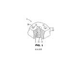
図1〜3を参照すると、台湾特許出願087216147号(公開番号392975号)に開示されているように、電気コネクタ1は、コンピュータ装置に使用される中央処理装置(「CPU」)とメインボードを電気的に相互接続するゼロ挿入力(「ZIF」)電気コネクタである。電気コネクタ1は、絶縁性ハウジング10と複数の導電性端子2とを有する。各導電性端子2は、その端にはんだボール23をあらかじめセットすることによって、表面実装技術(「SMT」)により回路基板30と電気的に接続する。 1-3, as disclosed in Taiwan Patent Application No. 087216147 (Publication No. 392975), the electrical connector 1 includes a central processing unit (“CPU”) used in a computer device and a main board. A zero insertion force (“ZIF”) electrical connector that is electrically interconnected. The electrical connector 1 has an
電気コネクタ1の絶縁性ハウジング10の下面は、回路基板30側に向けられ位置決めされた取付面12であり、上面は、電子部品を支承する支持面11である。また、絶縁性ハウジング10の取付面12と支持面11との間には複数のスルーホール13が貫通している。 The lower surface of the
対応するスルーホール13に収容された各導電性端子2は、支持面11に向かって延在する接触部20と、取付面12まで反対方向に延在する端部21とから成る。端部21の下面22は、対応するはんだボール23にはんだ付される。 Each
導電性端子2の端部21にはんだボール23をあらかじめセットする成功率を高めるために、端部21は接触部20に対して約90度の角度をなす円盤形平面であり、端部21と絶縁性ハウジング10の取付面12がほぼ同一の平面に配置される。端部21が平らな円盤形であることによってはんだボール23をあらかじめセットすることができる領域が広くなるため、はんだボール23は確実にあらかじめセットされる。更に、端部21の縁から複数の突起25が一体的に延在しており、これにより、はんだボール23が端部21の下面22からずれるのを防いでいる。 In order to increase the success rate of setting the
はんだボール23をあらかじめセットするSMTを利用するために、導電性端子2の一端の構造は、はんだボール23を容易に配置し接続することができるものでなければならない。導電性端子2の端部は、種々の解決策によってはんだボール23を配置し接続することができる様々な構造をとることができ、前述の方法はそのような解決策の1つに過ぎない。本発明は、はんだボール23の配置及び接続が改善された導電性端子を提供する。 In order to use the SMT in which the
本発明の目的は、はんだボールの配置を容易に行うことができる導電性端子及びその導電性端子を使用する電気コネクタを提供することである。 An object of the present invention is to provide a conductive terminal capable of easily arranging solder balls and an electrical connector using the conductive terminal.
本発明の他の目的は、はんだボールとはんだ付の確実性が向上した導電性端子を提供することである。 Another object of the present invention is to provide a conductive terminal with improved solder ball and soldering reliability.
本発明の導電性端子は、電子部品と回路基板との間の信号伝達が可能な電気コネクタの絶縁性ハウジングの複数の端子チャネル内に収容される。導電性端子は、第1の壁と、第1の壁と所定の角度で接続する第2の壁と、第2の壁と所定の角度で接続しかつ第1の壁と対向する第3の壁とを有する。導電性端子は、電子部品に電気接続される接触部と、はんだボールを介して回路基板に電気接続される取付部とを有する。取付部は、第1の壁の一端から湾曲して第3の壁に向かって延在する水平部と、第3の壁に形成され所定の角度で水平部に対応する鉛直部とを備える。水平部と鉛直部とがはんだボールに異なる二方向から接合しはんだボールが確実に位置決めされる。 The conductive terminal of the present invention is accommodated in a plurality of terminal channels of an insulating housing of an electrical connector capable of transmitting a signal between an electronic component and a circuit board. The conductive terminal includes a first wall, a second wall connected to the first wall at a predetermined angle, and a third wall connected to the second wall at a predetermined angle and facing the first wall. And a wall. The conductive terminal has a contact portion that is electrically connected to the electronic component, and a mounting portion that is electrically connected to the circuit board via a solder ball. The mounting portion includes a horizontal portion that curves from one end of the first wall and extends toward the third wall, and a vertical portion that is formed on the third wall and corresponds to the horizontal portion at a predetermined angle. The horizontal portion and the vertical portion are joined to the solder ball from two different directions, so that the solder ball is reliably positioned.
鉛直部と水平部の鉛直部側の側面との間に間隙が形成される。はんだボールが溶解すると錫(すず)がこの間隙(げき)に流れ込み、はんだボールと取付部の間のはんだ付の確実性が向上する。 A gap is formed between the vertical portion and the side surface of the horizontal portion on the vertical portion side. When the solder ball melts, tin flows into the gap, and the soldering reliability between the solder ball and the mounting portion is improved.
本発明の他の目的、特徴及び利点は、添付図面と関連して行われる以下の詳細な説明から明らかになるであろう。 Other objects, features and advantages of the present invention will become apparent from the following detailed description taken in conjunction with the accompanying drawings.
新規であると考えられる本発明の特徴は、添付の特許請求の範囲に詳細に説明される。本発明は、その目的及び利点とともに、添付図面と関連して行われる以下の説明を参照することによって最もよく理解することができる。図面において類似の参照符号は類似の要素を示す。 The features of the invention believed to be novel are set forth with particularity in the appended claims. The invention, together with its objects and advantages, can best be understood by referring to the following description taken in conjunction with the accompanying drawings. In the drawings, like reference numbers indicate like elements.
特定の実施形態を図面に示し本明細書に詳細に説明するが、本発明は様々な形態の実施形態をとることができ、本明細書の記載は発明の原理の例示であり、本発明は本明細書に記載し図示したものに限定されるものではないと理解されたい。 Although specific embodiments are shown in the drawings and are described in detail herein, the present invention can take various forms of embodiments, and the description herein is illustrative of the principles of the invention. It should be understood that the invention is not limited to what has been described and illustrated herein.
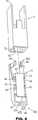
ここで、図4及び5を参照すると、電気コネクタに使用される本発明の導電性端子4は、従来技術と類似しており、電子部品(図示せず)と回路基板(図示せず)とを接続する。導電性端子4の端部には、はんだボール6があらかじめセットされる。 4 and 5, the conductive terminal 4 of the present invention used for an electrical connector is similar to the prior art, and includes an electronic component (not shown) and a circuit board (not shown). Connect.
電気コネクタは、絶縁性ハウジング5と、複数の導電性端子4とを含む。 The electrical connector includes an
絶縁性ハウジング5は、回路基板(コンピュータのマザーボード等)側に位置決めされる取付面51と、電子部品(中央処理装置(CPU)等)を支持する支持面52とを有する。絶縁性ハウジング5の取付面51と支持面52との間には複数の端子チャネル53が延在している。説明を分かりやすくするために、各図において示す絶縁性ハウジング5は1個の端子チャネル53を有するものとする。 The
各導電性端子4は、対応する端子チャネル53に収容される。導電性端子4は、第1の壁41と、該第1の壁41の一方の側部と約90度の角度をなして接続する第2の壁42と、該第2の壁42の他方の側部と約90度の角度をなして接続し第1の壁41と一定の距離で対向する第3の壁43とを有する。第1の壁41と第2の壁42との接続角部には複数の中空部44があり、これにより、第1の壁41と第2の壁42との接続角部の強度が弱まり、第1の壁41が中空部44に沿って容易に曲がるようになっている。同様に、第3の壁43と第2の壁42との接続角部には複数の中空部44があり、第3の壁43が中空部44に沿って第2の壁42の方に容易に曲がるようになっている。各導電性端子4が、対応する端子チャネル53に収容されると、取付面51に隣接する導電性端子4の一端部は取付部401となり、導電性端子4の取付部401とは反対側の支持面52に隣接する部分は接触部402となる。 Each conductive terminal 4 is accommodated in a corresponding
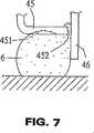
取付部401は、取付面51に隣接する第1の壁41の一端から第3の壁43に向けて約90度湾曲して延在する水平部45と、第3の壁43から延在し、約90度の角度で水平部45に対応する鉛直部46とを有する。図5を参照すると、水平部45と絶縁性ハウジング5の取付面51は略同一面内に存在する。鉛直部46は取付面51から延出し、はんだボール6を位置決めするためのL字状構造を水平部45と協同して形成している。 The
接触部402は、第1の壁41の一方の側に支持面52に隣接して形成された第1のばねアーム47と、第2の壁42の一方の側に支持面52に隣接して形成された第2のばねアーム48とを有する。第1のばねアーム47の自由端と第2のばねアーム48の自由端とは隣接して、電気要素(図示せず)の挿入部の挿入アームとなるばね収容構造を形成する。接触部402は本発明の新規性の要点ではなく、その電気接続の原理は、ZIF電気コネクタ(図示せず)の導電性端子の対応構造と類似しているので、ここでは詳しく説明しない。 The
図4〜6を参照すると、組立においては、導電性端子4は、絶縁性ハウジング5の取付面51からも絶縁性ハウジング5の対応する端子チャネル53に挿入することができ(図4参照)、絶縁性ハウジング5の支持面52からも絶縁性ハウジング5の対応する端子チャネル53に挿入することができる(図6参照)。導電性端子4を絶縁性ハウジング5の取付面51から絶縁性ハウジング5の対応する端子チャネル53に挿入する場合、導電性端子4の取付部401の鉛直部46を持って導電性端子4を挿入することができる。反対に、導電性端子4を絶縁性ハウジング5の支持面52から絶縁性ハウジング5の対応する端子チャネル53に挿入する場合、第2の壁42の一端に第1のばねアーム47と第2のばねアーム48に対応させて把持部49を形成し、これを持って導電性端子4を挿入することができる。 4-6, in assembly, the conductive terminal 4 can be inserted into the
図4及び5を参照すると、導電性端子4の取付部401は、その水平部45と鉛直部46とによってはんだボール6を位置決めする。はんだボール6が水平部45の表面に接触すると、鉛直部46は、水平部45に対し約90度の角度をなし水平部45と協同してL字状構造を形成しているため、はんだボール6が水平部45の延在方向に沿って移動するのを防ぐ。したがって、はんだボール6が、水平部45と鉛直部46とによって画定されたL字状スペースに置かれると、はんだボール6は水平部45及び鉛直部46とそれぞれ接続し、これらによって、異なる二方向の位置決めが行われる。したがって、はんだボール6は、水平部45の表面に正確に位置合せする必要はなく、容易に位置決めすることができる。 Referring to FIGS. 4 and 5, the
更に、はんだボール6の位置合せの正確性を向上させるため、水平部45に凹部451を形成する。はんだボール6が水平部45と接続すると、はんだボール6は水平部45の凹部451に収容されるため、はんだボール6の位置決めの確実性が向上する。 Furthermore, a
図7を参照すると、鉛直部46と水平部45の鉛直部46側の側面の間に間隙452が形成されている。はんだボール6が溶融すると、錫が間隙452に流れ込むため、はんだボール6を異なる二方向から水平部45及び鉛直部46の表面にそれぞれはんだ付することができるだけでなく、はんだボール6の錫の一部が間隙452を埋めて閉じ、はんだボール6と導電性端子4の取付部401の間をより確実にはんだ付することができる。 Referring to FIG. 7, a
導電性端子4は、第1の壁41、第2の壁42及び第3の壁43を有する。導電性端子4は、はんだボール6の位置決めの確実性が、第1の壁41から延在する水平部45と第3の壁43から延在する鉛直部46とによって形成されたL字状スペースによって向上している。鉛直部46と水平部45の鉛直部46側の側面との間に間隙452が形成され、溶融したはんだボール6の錫がこの間隙に入り込むため、はんだボール6のはんだ付の確実性が向上する。 The conductive terminal 4 has a
本発明をその例示的な実施形態に関して示し説明したが、当業者は、添付の特許請求の範囲に示したような本発明の趣旨及び範囲から逸脱することなく様々な変更、省略及び追加を行えると理解すべきである。 Although the invention has been shown and described with respect to exemplary embodiments thereof, those skilled in the art may make various changes, omissions and additions without departing from the spirit and scope of the invention as set forth in the appended claims. Should be understood.
Claims (7)
Translated fromJapanese第1の壁と、第1の壁と所定の角度で接続する第2の壁と、第2の壁と所定の角度で接続しかつ第1の壁と対向する第3の壁とを有し、
取付部は、第1の壁の一端から湾曲して第3の壁に向かって延在する水平部と、第3の壁に形成され所定の角度で水平部に対応する鉛直部とを備え、
該鉛直部は前記水平部のはんだボールとの接続面よりも延出し、前記鉛直部のはんだボールとの接続面と前記水平部のはんだボールとの接続面とがL字状構造を形成し、
前記鉛直部と水平部の鉛直部側の側面との間に間隙が形成され、
前記回路基板に電気接続する前にはんだボールが前記取付部に接合され、
前記水平部と鉛直部とがはんだボールに異なる二方向から接合してはんだボールを確実に位置決めする導電性端子。A contact portion that can be accommodated in an insulating housing and defined in a terminal channel defined between the electronic component and the circuit board; and a contact portion that is electrically connected to the electronic component; and a mounting portion that is electrically connected to the circuit board via a solder ball A conductive terminal comprising:
A first wall; a second wall connected to the first wall at a predetermined angle; and a third wall connected to the second wall at a predetermined angle and facing the first wall. ,
The mounting portion includes a horizontal portion that curves from one end of the first wall and extends toward the third wall, and a vertical portion that is formed on the third wall and corresponds to the horizontal portion at a predetermined angle.
The vertical portion extends from the connection surface of the horizontal portion with the solder ball, and the connection surface of the vertical portion with the solder ball and the connection surface of the horizontal portion with the solder ball form an L-shaped structure,
A gap is formed between the vertical part and the side of the horizontal part on the vertical part side,
Before the electrical connection to the circuit board, solder balls are joined to the mounting portion,
A conductive terminal for reliably positioning the solder ball by joining the horizontal portion and the vertical portion to the solder ball from two different directions.
回路基板に隣接する取付面と電子部品を支承するための支持面とを備え取付面及び支持面を貫通する複数の端子チャネルを画定する絶縁性ハウジングと、
対応する端子チャネル内にそれぞれ収容された複数の導電性端子とを有し、
導電性端子は、第1の壁と、第1の壁と接続する第2の壁と、第1の壁と対向して第2の壁と接続する第3の壁と、取付面に隣接する第1の壁の一端から湾曲して第3の壁に向かって延在する水平部と、所定の角度で水平部に対応し第3の壁から延在する鉛直部とを備え、
該鉛直部は前記水平部のはんだボールとの接続面よりも延出し、前記鉛直部のはんだボールとの接続面と前記水平部のはんだボールとの接続面とがL字状構造を形成し、
前記鉛直部と水平部の鉛直部側の側面との間に間隙が形成され、
前記回路基板に電気接続する前にはんだボールが接合され、
前記水平部と鉛直部とがはんだボールを確実に位置決めするための取付部を形成する電気コネクタ。An electrical connector for connecting an electronic component to a circuit board via a plurality of solder balls soldered to the circuit board,
An insulating housing having a mounting surface adjacent to the circuit board and a support surface for supporting the electronic component, and defining a plurality of terminal channels extending through the mounting surface and the support surface;
A plurality of conductive terminals each housed in a corresponding terminal channel;
The conductive terminal is adjacent to the first wall, the second wall connected to the first wall, the third wall facing the first wall and connected to the second wall, and the mounting surface. A horizontal portion curved from one end of the first wall and extending toward the third wall, and a vertical portion corresponding to the horizontal portion and extending from the third wall at a predetermined angle;
The vertical portion extends from the connection surface of the horizontal portion with the solder ball, and the connection surface of the vertical portion with the solder ball and the connection surface of the horizontal portion with the solder ball form an L-shaped structure,
A gap is formed between the vertical part and the side of the horizontal part on the vertical part side,
Solder balls are joined before electrical connection to the circuit board,
An electrical connector in which the horizontal portion and the vertical portion form an attachment portion for positioning the solder ball reliably.
Applications Claiming Priority (2)
| Application Number | Priority Date | Filing Date | Title |
|---|---|---|---|
| CNU032022816UCN2598181Y (en) | 2003-01-29 | 2003-01-29 | Conducting terminal and electric connector using same |
| PCT/US2004/002819WO2004068641A1 (en) | 2003-01-29 | 2004-01-29 | Conductive terminal and the electrical connector using the conductive terminal |
Publications (2)
| Publication Number | Publication Date |
|---|---|
| JP2006526251A JP2006526251A (en) | 2006-11-16 |
| JP4167265B2true JP4167265B2 (en) | 2008-10-15 |
Family
ID=29749115
Family Applications (1)
| Application Number | Title | Priority Date | Filing Date |
|---|---|---|---|
| JP2005518859AExpired - Fee RelatedJP4167265B2 (en) | 2003-01-29 | 2004-01-29 | Electrical connector using conductive terminal and conductive terminal |
Country Status (4)
| Country | Link |
|---|---|
| US (1) | US7297007B2 (en) |
| JP (1) | JP4167265B2 (en) |
| CN (1) | CN2598181Y (en) |
| WO (1) | WO2004068641A1 (en) |
Families Citing this family (12)
| Publication number | Priority date | Publication date | Assignee | Title |
|---|---|---|---|---|
| JP2007535094A (en) | 2003-07-16 | 2007-11-29 | グリフィクス インコーポレーティッド | Electrical interconnect assembly with interlocking contact system |
| US7297003B2 (en) | 2003-07-16 | 2007-11-20 | Gryphics, Inc. | Fine pitch electrical interconnect assembly |
| US7537461B2 (en) | 2003-07-16 | 2009-05-26 | Gryphics, Inc. | Fine pitch electrical interconnect assembly |
| CN200972994Y (en) | 2006-10-31 | 2007-11-07 | 富士康(昆山)电脑接插件有限公司 | Electric connector terminal |
| US7976319B2 (en)* | 2008-06-30 | 2011-07-12 | Tyco Electronics Corporation | Surface mount electrical connector having flexible solder tails |
| US7771244B1 (en)* | 2009-06-08 | 2010-08-10 | Lotes Co., Ltd | Electrical connector |
| US8899993B2 (en) | 2012-08-07 | 2014-12-02 | Amphenol InterCon Systems, Inc. | Interposer plate |
| US8708716B1 (en)* | 2012-11-12 | 2014-04-29 | Lotes Co., Ltd. | Electrical connector |
| US9825383B2 (en)* | 2015-04-27 | 2017-11-21 | Foxconn Interconnect Technology Limited | Shielded circuit board mounted connector having blade type contacts |
| CN205646233U (en)* | 2016-03-17 | 2016-10-12 | 富士康(昆山)电脑接插件有限公司 | Electric connector subassembly and electric connector thereof |
| US10431912B2 (en)* | 2017-09-29 | 2019-10-01 | Intel Corporation | CPU socket contact for improving bandwidth throughput |
| US10601195B2 (en)* | 2018-07-30 | 2020-03-24 | Lotes Co., Ltd | Electrical connector and electrical connector assembly capable of ensuring terminal positioning effect |
Family Cites Families (11)
| Publication number | Priority date | Publication date | Assignee | Title |
|---|---|---|---|---|
| TW392975U (en)* | 1998-09-29 | 2000-06-01 | Hon Hai Prec Ind Co Ltd | Electrical connector |
| TW422458U (en)* | 1999-04-09 | 2001-02-11 | Hon Hai Prec Ind Co Ltd | Electrical connector |
| US6257899B1 (en)* | 2000-07-26 | 2001-07-10 | Hon Hai Precision Ind. Co., Ltd. | Soft internal touch contact for IC socket |
| US6501665B1 (en)* | 2001-08-10 | 2002-12-31 | Lotes Co., Ltd. | Structure of a ball grid array IC mounting seat |
| US6530788B1 (en)* | 2001-10-09 | 2003-03-11 | Lotes Co., Ltd. | Structure of a ball grid array IC socket connection with solder ball |
| US6478637B1 (en)* | 2001-12-24 | 2002-11-12 | Hon Hai Precision Ind. Co., Ltd. | Contact for CPU socket |
| US6478599B1 (en)* | 2001-12-26 | 2002-11-12 | Hon Hai Precision Ind. Co., Ltd. | Contact for CPU socket |
| US6461183B1 (en)* | 2001-12-27 | 2002-10-08 | Hon Hai Precision Ind. Co., Ltd. | Terminal of socket connector |
| US6695628B2 (en)* | 2002-05-17 | 2004-02-24 | Hon Hai Precision Ind. Co., Ltd. | Battery connector |
| CN2598183Y (en)* | 2003-01-29 | 2004-01-07 | 莫列斯公司 | Conducting terminal and electric connector using same |
| US7001190B2 (en)* | 2004-04-26 | 2006-02-21 | Tyco Electronics Corporation | Repairable ball grid array contact |
- 2003
- 2003-01-29CNCNU032022816Upatent/CN2598181Y/ennot_activeExpired - Fee Related
- 2004
- 2004-01-29WOPCT/US2004/002819patent/WO2004068641A1/enactiveApplication Filing
- 2004-01-29JPJP2005518859Apatent/JP4167265B2/ennot_activeExpired - Fee Related
- 2004-01-29USUS10/537,928patent/US7297007B2/ennot_activeExpired - Fee Related
Also Published As
| Publication number | Publication date |
|---|---|
| US7297007B2 (en) | 2007-11-20 |
| WO2004068641A1 (en) | 2004-08-12 |
| US20060258200A1 (en) | 2006-11-16 |
| CN2598181Y (en) | 2004-01-07 |
| JP2006526251A (en) | 2006-11-16 |
Similar Documents
| Publication | Publication Date | Title |
|---|---|---|
| US6702594B2 (en) | Electrical contact for retaining solder preform | |
| US7125260B2 (en) | Mounting structure of connector | |
| US6155848A (en) | Auxiliary device for ZIF electrical connector | |
| JP2769638B2 (en) | Electrical connector and its electrical terminals | |
| US5997317A (en) | Ball grid array connector | |
| JP4143647B2 (en) | Electrical connector using conductive terminal and conductive terminal | |
| JP4167265B2 (en) | Electrical connector using conductive terminal and conductive terminal | |
| JP2003203735A (en) | Socket connector | |
| JP2003197299A (en) | Surface mount rectanglular electric connector | |
| KR20060126356A (en) | LIF socket connector | |
| US6135784A (en) | LIF PGA socket | |
| JP2003178844A (en) | Coaxial connector | |
| US6450826B1 (en) | Contact of electrical connector | |
| JP4230489B2 (en) | Electrical connector using conductive terminal and conductive terminal | |
| US8052433B2 (en) | Electrical connector having retention means arranged adjacent to passageway for holding fusible member thereto | |
| JP2002175855A (en) | connector | |
| TW201911673A (en) | Electrical connector and method of making the same | |
| CN201549675U (en) | Electrical connectors and their conductive terminals | |
| JP2672661B2 (en) | PCB mounted connector | |
| JP2004103491A (en) | Surface mount type connector | |
| US6382984B1 (en) | Electrical card connector for solderlessly electrically connecting to a printed circuit board | |
| CN2736972Y (en) | Electric connector | |
| CN210723446U (en) | Electrical connector | |
| CN212392407U (en) | Connectors and their terminals | |
| TWM640940U (en) | Insulation displacement connector and cable component comprising the same |
Legal Events
| Date | Code | Title | Description |
|---|---|---|---|
| A977 | Report on retrieval | Free format text:JAPANESE INTERMEDIATE CODE: A971007 Effective date:20070907 | |
| A131 | Notification of reasons for refusal | Free format text:JAPANESE INTERMEDIATE CODE: A131 Effective date:20070918 | |
| A521 | Request for written amendment filed | Free format text:JAPANESE INTERMEDIATE CODE: A523 Effective date:20071203 | |
| A131 | Notification of reasons for refusal | Free format text:JAPANESE INTERMEDIATE CODE: A131 Effective date:20080205 | |
| A601 | Written request for extension of time | Free format text:JAPANESE INTERMEDIATE CODE: A601 Effective date:20080507 | |
| A602 | Written permission of extension of time | Free format text:JAPANESE INTERMEDIATE CODE: A602 Effective date:20080514 | |
| A601 | Written request for extension of time | Free format text:JAPANESE INTERMEDIATE CODE: A601 Effective date:20080604 | |
| A602 | Written permission of extension of time | Free format text:JAPANESE INTERMEDIATE CODE: A602 Effective date:20080611 | |
| A521 | Request for written amendment filed | Free format text:JAPANESE INTERMEDIATE CODE: A523 Effective date:20080623 | |
| TRDD | Decision of grant or rejection written | ||
| A01 | Written decision to grant a patent or to grant a registration (utility model) | Free format text:JAPANESE INTERMEDIATE CODE: A01 Effective date:20080729 | |
| A01 | Written decision to grant a patent or to grant a registration (utility model) | Free format text:JAPANESE INTERMEDIATE CODE: A01 | |
| A61 | First payment of annual fees (during grant procedure) | Free format text:JAPANESE INTERMEDIATE CODE: A61 Effective date:20080731 | |
| R150 | Certificate of patent or registration of utility model | Free format text:JAPANESE INTERMEDIATE CODE: R150 | |
| FPAY | Renewal fee payment (event date is renewal date of database) | Free format text:PAYMENT UNTIL: 20110808 Year of fee payment:3 | |
| LAPS | Cancellation because of no payment of annual fees |