JP4166516B2 - Disk array device - Google Patents
Disk array deviceDownload PDFInfo
- Publication number
- JP4166516B2 JP4166516B2JP2002174949AJP2002174949AJP4166516B2JP 4166516 B2JP4166516 B2JP 4166516B2JP 2002174949 AJP2002174949 AJP 2002174949AJP 2002174949 AJP2002174949 AJP 2002174949AJP 4166516 B2JP4166516 B2JP 4166516B2
- Authority
- JP
- Japan
- Prior art keywords
- control board
- backboard
- controller
- disk array
- resource management
- Prior art date
- Legal status (The legal status is an assumption and is not a legal conclusion. Google has not performed a legal analysis and makes no representation as to the accuracy of the status listed.)
- Expired - Fee Related
Links
Images


Classifications
- G—PHYSICS
- G06—COMPUTING OR CALCULATING; COUNTING
- G06F—ELECTRIC DIGITAL DATA PROCESSING
- G06F11/00—Error detection; Error correction; Monitoring
- G06F11/30—Monitoring
- G06F11/32—Monitoring with visual or acoustical indication of the functioning of the machine
- G06F11/324—Display of status information
- G06F11/325—Display of status information by lamps or LED's
- G—PHYSICS
- G06—COMPUTING OR CALCULATING; COUNTING
- G06F—ELECTRIC DIGITAL DATA PROCESSING
- G06F11/00—Error detection; Error correction; Monitoring
- G06F11/30—Monitoring
- G06F11/3003—Monitoring arrangements specially adapted to the computing system or computing system component being monitored
- G06F11/3034—Monitoring arrangements specially adapted to the computing system or computing system component being monitored where the computing system component is a storage system, e.g. DASD based or network based
- G—PHYSICS
- G06—COMPUTING OR CALCULATING; COUNTING
- G06F—ELECTRIC DIGITAL DATA PROCESSING
- G06F11/00—Error detection; Error correction; Monitoring
- G06F11/30—Monitoring
- G06F11/3055—Monitoring arrangements for monitoring the status of the computing system or of the computing system component, e.g. monitoring if the computing system is on, off, available, not available
- G—PHYSICS
- G06—COMPUTING OR CALCULATING; COUNTING
- G06F—ELECTRIC DIGITAL DATA PROCESSING
- G06F11/00—Error detection; Error correction; Monitoring
- G06F11/30—Monitoring
- G06F11/3058—Monitoring arrangements for monitoring environmental properties or parameters of the computing system or of the computing system component, e.g. monitoring of power, currents, temperature, humidity, position, vibrations
- G—PHYSICS
- G11—INFORMATION STORAGE
- G11B—INFORMATION STORAGE BASED ON RELATIVE MOVEMENT BETWEEN RECORD CARRIER AND TRANSDUCER
- G11B27/00—Editing; Indexing; Addressing; Timing or synchronising; Monitoring; Measuring tape travel
- G11B27/002—Programmed access in sequence to a plurality of record carriers or indexed parts, e.g. tracks, thereof, e.g. for editing
- G—PHYSICS
- G11—INFORMATION STORAGE
- G11B—INFORMATION STORAGE BASED ON RELATIVE MOVEMENT BETWEEN RECORD CARRIER AND TRANSDUCER
- G11B27/00—Editing; Indexing; Addressing; Timing or synchronising; Monitoring; Measuring tape travel
- G11B27/10—Indexing; Addressing; Timing or synchronising; Measuring tape travel
- G11B27/34—Indicating arrangements
- G—PHYSICS
- G11—INFORMATION STORAGE
- G11B—INFORMATION STORAGE BASED ON RELATIVE MOVEMENT BETWEEN RECORD CARRIER AND TRANSDUCER
- G11B27/00—Editing; Indexing; Addressing; Timing or synchronising; Monitoring; Measuring tape travel
- G11B27/36—Monitoring, i.e. supervising the progress of recording or reproducing
- G—PHYSICS
- G11—INFORMATION STORAGE
- G11B—INFORMATION STORAGE BASED ON RELATIVE MOVEMENT BETWEEN RECORD CARRIER AND TRANSDUCER
- G11B33/00—Constructional parts, details or accessories not provided for in the other groups of this subclass
- G11B33/12—Disposition of constructional parts in the apparatus, e.g. of power supply, of modules
- G11B33/125—Disposition of constructional parts in the apparatus, e.g. of power supply, of modules the apparatus comprising a plurality of recording/reproducing devices, e.g. modular arrangements, arrays of disc drives
- G11B33/127—Mounting arrangements of constructional parts onto a chassis
- G11B33/128—Mounting arrangements of constructional parts onto a chassis of the plurality of recording/reproducing devices, e.g. disk drives, onto a chassis
- G—PHYSICS
- G11—INFORMATION STORAGE
- G11B—INFORMATION STORAGE BASED ON RELATIVE MOVEMENT BETWEEN RECORD CARRIER AND TRANSDUCER
- G11B2220/00—Record carriers by type
- G11B2220/20—Disc-shaped record carriers
- G—PHYSICS
- G11—INFORMATION STORAGE
- G11B—INFORMATION STORAGE BASED ON RELATIVE MOVEMENT BETWEEN RECORD CARRIER AND TRANSDUCER
- G11B2220/00—Record carriers by type
- G11B2220/40—Combinations of multiple record carriers
- G11B2220/41—Flat as opposed to hierarchical combination, e.g. library of tapes or discs, CD changer, or groups of record carriers that together store one title
- G11B2220/415—Redundant array of inexpensive disks [RAID] systems
Landscapes
- Engineering & Computer Science (AREA)
- Theoretical Computer Science (AREA)
- Physics & Mathematics (AREA)
- Computing Systems (AREA)
- Quality & Reliability (AREA)
- General Engineering & Computer Science (AREA)
- General Physics & Mathematics (AREA)
- Mathematical Physics (AREA)
- Power Sources (AREA)
- Debugging And Monitoring (AREA)
Description
Translated fromJapanese【0001】
【発明の属する技術分野】
この発明は、ディスクアレイ装置に関する。
【0002】
【発明の背景】
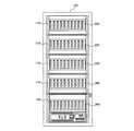
ラックマウント型のディスクアレイシステムの従来例を図9の正面図に示す。同図に示すように、ディスクアレイシステムは、要求される性能や仕様により、ディスクアレイ装置を構成する基本筐体(正ディスクアレイ装置)100に加え、ディスクドライブを増設すべく増設筐体(副ディスクアレイ装置)110を一台もしくは複数台備える。具体的には、ラックフレーム120内に基本筐体100及び増設筐体110を収容することで、ディスクアレイシステムを構成する。これら基本筐体100及び増設筐体110には、ディスクアレイ装置の各種機能を提供するボード(基板)やユニットが装備されている。
【0003】
従来、コントローラモジュールの他に、エンクロージャ(ENCLOSURE)と呼ばれる資源管理部を設け、専用の基板を用いてモジュール化していた。このエンクロージャとは、いくつかの機能を備えており、その一つは、増設筐体を追加してディスクアレイ装置を増設した場合に、各筐体内の各ハードディスクドライブモジュールへのアクセス制御を統合するための管理機能を有する。すなわち、エンクロージャは、各筐体内の各ハードディスクドライブ等の資源の状態に関する管理情報を収集し、監視する。基本筐体(正ディスクアレイ装置)は、コントローラに加え、このエンクロージャ(資源管理部)を有するが、増設筐体(副ディスクアレイ装置)は、エンクロージャ(副資源管理部)を備えればよく、コントローラを有する必要はない。
【0004】
具体的には、図8のブロック図に示すように、基本筐体100側のエンクロージャは、各ハードディスクドライブの状態の監視機能を実現すべく、コントローラ71とディスクドライブ200との間を結ぶファイバチャネルループ(FC-AL,Fibre Chanel Arbitration Loop)のスイッチ制御を行う。このエンクロージャにおけるファイバーループスイッチ(Fibre Loop Switch)機能はチップ化されたポートバイパス回路(Port Bypass Circuit,以下、PBCと称する)で実現される。一方、増設筐体110側のエンクロージャ(副資源管理部)は、基本筐体100側のエンクロージャとファイバチャネルループPBC、及び配線60,91で接続される。このことにより、増設筐体110側のディスクドライブ200等の資源に関する管理情報を収集し、監視することができる。
【0005】
この他、エンクロージャは、資源として、ディスクアレイ装置の動作状態を示す表示ランプ、電源モジュール、及びファンモジュールと、電気的に接続されるべく配線されており、各モジュールの状態に関するデータを取得したり、制御信号を送信する。すなわち、エンクロージャは、電源モジュールの監視機能、ディスクアレイ装置の動作状態を示す表示ランプの制御機能、及び筐体内の温度を監視してファンモジュールを制御する機能を有する。電源モジュールの監視機能としては、その運転状態の監視やオン/オフの制御を行う。図8では、これら各モジュールとのデータ及び制御信号は、資源管理情報として示されている。
【0006】
基本筐体100及び増設筐体110のエンクロージャによる資源機能の一つとして、ディスクドライブ200及び電源モジュールのディスクアレイ装置に対する装着状態に関するデータを収集し、このデータに基づき装着状態をコントローラに通知する。
このようなエンクロージャの各種機能は、エンクロージャ制御部として専用のLSI、マイコン、及びPBCにより実現される。
【0007】
【発明が解決しようとする課題】
図8の基本筐体におけるエンクロージャを単体の独立したモジュールとして実装することは、ディスクアレイ装置の小型化の阻害要因となっていた。特に、2Gbps等の高速伝送時には、波形品質を保つ為に数台のドライブ毎にCDR(Clock Data Recovery)を追加する必要がある。よって、ファイバーループスイッチ機能を実現するPBCの1チップあたりのCDRの数は制限されるため、PBCを実装する数が増えてしまい、小型化がさらに阻害される場合が多い。
【0008】
【課題を解決するための手段】
少なくとも、複数のディスクドライブと、前記ディスクドライブの制御部を有する制御基板とが一つの筐体に収容された正ディスクアレイ装置を備えたディスクアレイシステムにおける前記正ディスクアレイ装置の基板構造であって、
前記筐体内の資源を管理する資源管理部を前記正ディスクアレイ装置の前記制御基板に実装したことを特徴とするディスクアレイ装置の基板構造。
その他、本願が開示する課題、及びその解決方法は、発明の実施の形態の欄及び図面により明らかにされる。
【0009】
【発明の実施の形態】
本明細書の記載により、少なくとも次のことが明らかにされる。
前記ディスクアレイシステムは、少なくとも複数のディスクドライブが別の筐体に収容された増設用の副ディスクアレイ装置を更に備えたこととできる。
【0010】
前記資源管理部を二重化すべく、前記正ディスクアレイ装置は、前記筐体内の資源を管理する副資源管理部を実装した基板を備えたこととできる。
【0011】
前記基板の前記副資源管理部は、前記制御基板の前記制御部と電気的に接続されており、前記副資源管理部は前記制御部によって制御されることとできる。
【0012】
前記複数のディスクドライブは、相互にループを介して電気的に接続されており、前記制御基板の前記制御部が前記ループを通じて前記複数のディスクドライブに接続するのであって、前記制御基板の前記資源管理部は、前記ループによる前記接続の関係を切り替えるスイッチ制御を行うこととできる。
【0013】
前記ループは、ポートバイパス回路としてチップ化されて別の基板に実装されてなることとできる。
【0014】
前記制御基板の前記資源管理部は、前記ディスクアレイシステムの動作状態に関するデータを収集し、前記データに基づき前記動作状態を表示するランプの点灯を制御することとできる。
【0015】
前記制御基板の前記資源管理部は、前記ディスクアレイシステムの動作状態に関するデータを収集するにあたり、前記複数のディスクドライブにおける所定のディスクドライブを介して前記データを収集することとできる。
【0016】
前記制御基板の前記資源管理部は、前記複数のディスクドライブと、少なくとも前記ディスクドライブへ電源を供給する電源装置と電気的に接続されており、前記資源管理部は、前記複数のディスクドライブ及び前記電源装置の前記ディスクアレイ装置に対する装着状態に関するデータを収集し、前記データに基づき前記装着状態を前記制御部に通知することとできる。
【0017】
ディスクアレイ装置は、前記基板構造を有する前記正ディスクアレイ装置である。
【0018】
ディスクアレイシステムは、前記基板構造を有する前記正ディスクアレイ装置と前記副ディスクアレイ装置とを備える。
【0019】
以下、各実施例について、発明の背景の項で説明した事項と共通する事項は、重複するため省略し、発明の特徴に関する部分を中心に説明する。
【0020】
=====ディスクアレイ装置の構成=====
基本筐体としてのディスクアレイ装置の構成例を図1の正面側斜視図や図2の背面側斜視図に示す。図1に示すように、基本筐体を構成するシャーシ100には、通気性を有する前面飾り扉300が取り外し可能に取り付けられている。この前面飾り扉300には3列単位でルーバ301が取り外し可能にはめ込まれている。
【0021】
また、図1に示すように、基本筐体100を構成するシャーシの前面開口部には、左側から順番にハードディスクドライブのモジュール200(以下、HDDモジュールと記す)が取り外し可能に整列して配置されている。その取り外しは、各HDDモジュール200のハンドル部分201を持って行う。各HDDモジュール200は、内部に記録媒体として3.5インチ(約88.9mm)のディスクを備えており、ディスクの直径方向が高さ方向になるように配置される。シャーシ100は、前面開口部側に例えば14台のHDDモジュール200を格納する。
【0022】
さらに、シャーシの前面開口部の右側の1列には、操作パネルのモジュール400(以下、操作モジュールと記す)とバッテリのモジュール500(以下、バッテリモジュールと記す)が格納される。このバッテリモジュール500は、二次電池が内蔵され、定期的な交換が容易なように、シャーシの前面に配置されている。
【0023】
図2に示すように、ディスクアレイ装置を後面左方向から見ると、シャーシは後面部が開口しており、左右の両側面側にはファンモジュール800が脱着可能に配置されている。ファンモジュール800はシャーシの内部を冷却する。左右それぞれのファンモジュール800の背面部には排気のためのスリット801が設けられており、このスリット801から熱を放出する。このファンモジュール800により、外気が前面飾り扉300を通してシャーシ内に取り込まれ、シャーシ後部より排出される。
【0024】
図2に示すように、これら左右のファンモジュール800に挟まれる位置に、2台の電源のモジュール600(以下、電源モジュールと記す)が配置されている。電源モジュール600の下部には上下に2台のコントローラ(制御部)のモジュール700、702(以下、コントローラモジュールと記す)が配置されている。電源モジュール600、コントローラモジュール700、702はそれぞれ脱着可能である。なお、ファンモジュール800、電源モジュール(電源装置)600、及びコントローラモジュール700、702は全て2台ずつ備えている必要はなく、それぞれ1台のみでもディスクアレイ装置は稼働可能である。コントローラモジュール700、702は、ディスクアレイシステムを例えばRAID方式で制御するモジュールであり、この制御機能を実現する回路基板(制御基板)を実装している。
【0025】
ディスクアレイ装置の内部構造について説明する。図2のB−B断面でディスクアレイ装置を上方から見たときの内部の概略を図5に示す。また、図2のC−C断面でディスクアレイ装置を側方から見たときの内部の概略を図7に示す。バックボードと称する仕切り用基板900の後方には、コントローラモジュール700を接続するためのもう一枚のバックボード906が設けられている。以後、シャーシ前面側のバックボードを前面側バックボード900、コントローラモジュール700が接続されるバックボードを後面側バックボード905と呼ぶ。後面側バックボード905にはコネクタ906が備えられ、コントローラモジュール700のコネクタ701と接続される。また、前面側バックボード900と後面側バックボード905は相互にコネクタ908、909で結合される。
【0026】
コントローラモジュール700は、シャーシの後方から脱着可能に取り付けられている。内部には、前述したように、CPUや、メモリ、キャッシュ等を備えた制御基板を有している。さらに、ディスクアレイ装置の増設管理を行うエンクロージャの機能も備えている。コントローラモジュール700は、後面側バックボード905を介してディスクアレイ装置内の各モジュールと接続されており、各モジュールの制御、管理を行う。
【0027】
シャーシの前面開口部側にはHDDモジュール200が配置され、前面側バックボード900に接続されている。シャーシの後面開口部側には上部に電源モジュール600、下部にコントローラモジュール700、702が配置される。電源モジュール600は前面側バックボード900に接続され、コントローラモジュール700、702は後面側バックボード905に接続される。
【0028】
前面側バックボード900と後面側バックボード905は、相互にコネクタ908、909で接続されている。前面側バックボード900と後面側バックボード905間の情報のやりとりは、コネクタ908、909を介して行われる。
【0029】
これらのバックボードはバックボード固定枠に固定されてバックボードアッセンブリ912を構成している。また、後面側バックボード905には2枚のコントローラモジュール700、702を接続するためのコネクタ906、907が配置されている。コネクタ906はコントローラモジュール700を接続するためのコネクタであり、コネクタ907はコントローラモジュール702を接続するためのコネクタである。コントローラモジュール700と702は、相互にキャッシュデータを共有しており、モジュール間で高速なデータ転送を行うことが必要である。コネクタ906とコネクタ907は、後面側バックボード905上において、相互に対応するピンの位置が上下の同一位置になるように配置される。そのため、ピン間を結ぶ後面側バックボード905上のパターン配線の長さを最短にできる。これによりコントローラモジュール700と702の間での高速データ転送が実現可能となり、キャッシュの共有化が可能となる。
【0030】
図2のA−A断面でディスクアレイ装置を上方から見たときの内部の概略を図4に示す。前面側バックボード900には、2台の電源モジュールを接続可能とするためのコネクタ903と、2台のファンモジュールを接続可能とするためのコネクタ901が配置される。ファンモジュール800は、シャーシの右側面側に装着されるものと、左側面側に装着されるものは区別無く同一のものが使用される。そのため、前面側バックボード900上において、ファンモジュール800接続用コネクタ901の位置が右側用と左側用で上下に異なった配置となっている。
【0031】
=====第一実施例=====
本実施例では、図3のブロック図に示すように、基本筐体100側のディスクアレイ装置(正ディスクアレイ装置)のコントローラ(制御部)の基板(制御基板、以下、コントローラ基板と称す)11上にエンクロージャ部(資源管理部)13を実装することで、コントローラモジュール内にエンクロージャの機能を集約する。このことで、エンクロージャ専用の基板や、そのモジュールを省略することができ、ディスクアレイ装置及びディスクアレイシステムの小型化が図れる。
【0032】
具体的な構成としては、RAID方式のディスクアレイシステムを制御し、ホスト制御の機能を担うコントローラ部12と、ドライブ制御機能を担うエンクロージャ部13とを共通のコントローラモジュール(基板)に集約する。コントローラ部12は、ホスト制御部として外部のホストとのデータ入出力を制御する。エンクロージャ部13は、ドライブ制御部として、前述したように、各筐体内の各ディスクドライブの動作状態を監視し、制御する。
【0033】
ホストとのデータの入出力を可能とすべく、コントローラ12とディスクドライブ200との間はファイバチャネルループで接続されている。一方、エンクロージャ部13がディスクドライブ200の管理情報を収集可能とすべく、SES(SCSI Enclosure Service)用の二つの資源管理用ドライブ200aとエンクロージャ部13との間は、所定のインタフェースを介して接続される。このインタフェースは、例えば「SFF8067」と称される規格に則っており、ESI(Enclosure Service I/F)と称される。
【0034】
コントローラ基板700上には、ホスト制御部としての機能を実現すべく、ファイバープロトコルチップ(FPC)と称されるLSI及び周辺回路(S/P, シリアル-パラレル変換用回路)が実装されている。このコントローラ基板700上には、ホスト制御部を含むエンクロージャ部13としての機能を実現すべく、LSIやマイコン及びPBCが実装される。LSIは、前述した資源に関する情報を管理する機能と、ESIのハードウエア部分の機能とを司る。マイコンは、ESIのソフトウエア部分の他、各種の制御を司る。PBCは、ドライブバイパスの制御として、ファイバチャネルループ(FC-AL, Fibre Chanel Arbitration Loop)のスイッチ制御を行う。
【0035】
技術思想としての発明についての実施例の説明の便宜上、基本筐体においてコントローラ(モジュール)が一つの場合(シングルコントローラ方式)で説明したが、コントローラ(モジュール)を二つとした構成(デュアルコントローラ方式)にも適用可能である。このデュアルコントローラ方式の目的は、コントローラのモジュールを二重化することで、コントローラ及びエンクロージャの機能を冗長化し、ディスクアレイ装置の信頼性を担保することにある。すなわち、図6に示すように、基本筐体100において、二つのコントローラ基板(図中、CTL0及び CTL1)それぞれに共通の機能としてエンクロージャ部を設けることができる。
【0036】
=====第二実施例=====
前述した第一実施例では、コントローラ部12とエンクロージャ部13とを共通のモジュールで実現する点を中心に説明した。しかしながら、シングルコントローラ方式の場合、コントローラ部12及びエンクロージャ部13の双方について冗長性がなくなってしまう。そこで、重要なドライブ制御部を担うエンクロージャ部13については、冗長性を担保すべく、基板上にエンクロージャ部13のみを搭載したモジュールを用意する。このことで、信頼性の向上を図ることができる。
【0037】
基本的な構成としては、図6に示すディスクアレイシステムにおいて、図中右側に示される一方のコントローラ(モジュール)の基板700上から、破線で囲まれたコントローラ部12を省略して実質的にシングルコントローラ方式とし、エンクロージャ部13のみを残す。
【0038】
このような構成により、一方のエンクロージャ部13に障害が発生した場合、他方のエンクロージャ部13が代行して、エンクロージャの機能を担保できる。
【0039】
詳しくは、図6に示すデュアルコントローラ方式では、基本筐体における二つのコントローラ基板700のエンクロージャ部13間において、そのPBCが互いに接続されている。この接続関係を残したまま、シングルコントローラ方式に変更する。すなわち、一方のコントローラ基板700において、点線で囲まれた部分(図中においてコントローラ部12に相当)を実装せず、一方のコントローラ部12を省略し、エンクロージャ部13のみを残した構成のエンクロージャボードとする。このことで、シングルコントローラ方式でエンクロージャ部13に冗長性を持たせた構成とできる。
【0040】
そして、もともとデュアルコントローラ方式であった構成において相互のエンクロージャ13間がPBCを通じ接続されている。すなわち、デュアルコントローラ方式では、図6に示されるように、二つのコントローラ基板11上の各エンクロージャ部13の間は、互いのPBCがバックボード(別の基板、図中、「B/B」で示される)上に実装されたファイバチャネルループ(FC-AL)及びこのループに接続された資源管理用ドライブを介して接続されている。このため、そのまま、コントローラボードのコントローラ部から他方のエンクロージャボードのエンクロージャ部を制御することが可能である。
【0041】
したがって、このような二つのコントローラボードを用いたシングルコントローラ方式、あるいは、もともとのデュアルコントローラ方式としても、コントローラ部から共通の制御が可能となる。
【0042】
=====第三実施例=====
基本筐体のコントローラ基板に実装されたエンクロージャ部の構成要素であるファイバチャネルループ(FC-AL)を実現するPBCの実装について説明する。このPBCが、一枚のコントローラ基板上に収まりきらず、バックボード(B/B)と称される仕切用基板に実装された実施例を説明する。本実施例について、図6にブロック回路図を示し、図2のC-C線断面を側方からみた断面図を図7に示す。
【0043】
同図に示すように、シャーシの前面開口部側にはHDDモジュール200が配置され、前面側バックボード900に接続されている。シャーシの後面開口部側には上部に電源モジュール600、下部にコントローラモジュール700、702が配置される。電源モジュール600は前面側バックボード900に接続され、コントローラモジュール700、702は後面側バックボード905に接続される。前面側バックボード900と後面側バックボード905は、相互にコネクタ908、909で接続されている。前面側バックボード900と後面側バックボード905間の情報のやりとりは、コネクタ908、909を介して行われる。
【0044】
図3を参照して第一実施例で説明したように、エンクロージャ部の構成要素であるファイバチャネルループは、実装上、PBCの形態で実現される。このPBCの部分は、基本筐体の小型化の要請上、コントローラ基板に収めず、バックボードに実装する。図6にブロック回路図では、B/Bで示されるバックボード上にファイバチャネルループ(PBC)が示される。
【0045】
そこで、図7に示す断面図では、バックボード900の実装面上の空いた領域、つまり他のモジュールや基板類の邪魔にならない空き領域を有効活用してPBCを実装する。図中「PBC」で示されるように、PBCは、実装やPBCの機能及び実装の効率の観点から、バックボード900の両面にそれぞれ設けられる。
【0046】
このような実装構造により、エンクロージャ基板(モジュール)を省略して基本筐体の小型化を図りつつ、その上で更に、コントローラ基板(モジュール)700に実装したエンクロージャ部のうち、ファイバチャネルループを担うPBCをバックボードの空き領域に実装する。その分、コントローラ基板700の小型化を図ることができ、基本筐体の小型化に寄与できる。このことで、エンクロージャ部の冗長性を担保しながら、基本筐体としてのディスクアレイ装置及びディスクアレイシステムを小型化できる。
【0047】
以上、本発明について、その実施の形態に基づき具体的に説明したが、これに限定されるものではなく、その要旨を逸脱しない範囲で種々変更可能である。
【0048】
【発明の効果】
エンクロージャ部の冗長性を担保しながら、基本筐体としてのディスクアレイ装置及びディスクアレイシステムを小型化できる。
【図面の簡単な説明】
【図1】 本実施の一形態に係る基本筐体としてのディスクアレイ装置の正面側斜視図である。
【図2】 本実施の一形態に係る基本筐体としてのディスクアレイ装置の背面側斜視図である。
【図3】 本発明の一実施の形態に係るディスクアレイシステムの回路ブロック図である。
【図4】 図2のA−A断面でディスクアレイ装置を上方から見たときの内部構造を示す図である。
【図5】 図2のB−B断面でディスクアレイ装置を上方から見たときの内部構造を示す図である。
【図6】 本発明の一実施の形態に係るデュアルコントローラ方式ディスクアレイシステムの回路ブロック図である。
【図7】 図2のC−C断面でディスクアレイ装置を側方から見たときの内部構造を示す図である。
【図8】 従来のディスクアレイシステムの回路ブロック図である。
【図9】 ストレージシステムの全体構成を示す正面図である。
【符号の説明】
12 コントローラ部(制御部)
13 エンクロージャ部(資源管理部)
100 基本筐体(正ディスクアレイ装置)
110 増設筐体(副ディスクアレイ装置)
120 ラックフレーム
200 ディスクドライブ
200a 資源管理用ドライブ
900 前面側バックボード
905 後面側バックボード
600 電源モジュール
700 コントローラモジュール
800 ファンモジュール
700 コントローラ基板(制御基板)
B/B バックボード、別の基板
PBC Port Bypass Circuit,ポートバイパス回路
FC-AL ファイバチャネルループ[0001]
BACKGROUND OF THE INVENTION
The present invention relates to a disk array device.
[0002]
BACKGROUND OF THE INVENTION
A conventional example of a rack mount type disk array system is shown in the front view of FIG. As shown in the figure, the disk array system has an additional enclosure (secondary disk) to add disk drives in addition to the basic enclosure (primary disk array apparatus) 100 constituting the disk array apparatus, depending on the required performance and specifications. One or a plurality of (disk array devices) 110 are provided. Specifically, the disk array system is configured by housing the
[0003]
Conventionally, in addition to the controller module, a resource management unit called an enclosure (ENCLOSURE) is provided and modularized using a dedicated board. This enclosure has several functions, one of which integrates access control to each hard disk drive module in each enclosure when an additional enclosure is added and a disk array device is added. Management function. That is, the enclosure collects and monitors management information related to the state of resources such as hard disk drives in each housing. The basic chassis (primary disk array device) has this enclosure (resource management unit) in addition to the controller, but the additional chassis (secondary disk array device) only needs to have an enclosure (secondary resource management unit). There is no need to have a controller.
[0004]
Specifically, as shown in the block diagram of FIG. 8, the enclosure on the side of the
[0005]
In addition, the enclosure is wired as a resource so as to be electrically connected to an indicator lamp, a power supply module, and a fan module that indicate the operation status of the disk array device, and acquires data on the status of each module. , Send a control signal. That is, the enclosure has a monitoring function of the power supply module, a control function of a display lamp indicating the operation state of the disk array device, and a function of controlling the fan module by monitoring the temperature in the casing. As a monitoring function of the power supply module, the operation state is monitored and on / off control is performed. In FIG. 8, data and control signals with these modules are shown as resource management information.
[0006]
As one of resource functions by the enclosures of the
Various functions of such an enclosure are realized by a dedicated LSI, microcomputer, and PBC as an enclosure control unit.
[0007]
[Problems to be solved by the invention]
The mounting of the enclosure in the basic casing of FIG. 8 as a single independent module has been an obstacle to downsizing the disk array device. In particular, during high-speed transmission such as 2 Gbps, it is necessary to add CDR (Clock Data Recovery) for each of several drives in order to maintain waveform quality. Therefore, since the number of CDRs per chip of the PBC that realizes the fiber loop switch function is limited, the number of PBCs to be mounted increases, and the downsizing is often further hindered.
[0008]
[Means for Solving the Problems]
A substrate structure of the primary disk array device in a disk array system including a primary disk array device in which at least a plurality of disk drives and a control board having a control unit of the disk drive are housed in a single housing. ,
A substrate structure of a disk array device, wherein a resource management unit for managing resources in the housing is mounted on the control substrate of the primary disk array device.
In addition, the problems disclosed by the present application and the solutions thereof will be clarified by the embodiments of the present invention and the drawings.
[0009]
DETAILED DESCRIPTION OF THE INVENTION
At least the following will be clarified by the description of the present specification.
The disk array system may further include an additional secondary disk array device in which at least a plurality of disk drives are housed in a separate housing.
[0010]
In order to duplicate the resource management unit, the primary disk array device may include a substrate on which a secondary resource management unit that manages resources in the chassis is mounted.
[0011]
The secondary resource management unit of the board may be electrically connected to the control unit of the control board, and the secondary resource management unit may be controlled by the control unit.
[0012]
The plurality of disk drives are electrically connected to each other through a loop, and the control unit of the control board connects to the plurality of disk drives through the loop, and the resource of the control board The management unit can perform switch control for switching the connection relationship by the loop.
[0013]
The loop may be formed as a chip as a port bypass circuit and mounted on another substrate.
[0014]
The resource management unit of the control board can collect data relating to an operation state of the disk array system, and control lighting of a lamp that displays the operation state based on the data.
[0015]
The resource management unit of the control board can collect the data via a predetermined disk drive in the plurality of disk drives when collecting the data relating to the operation state of the disk array system.
[0016]
The resource management unit of the control board is electrically connected to the plurality of disk drives and at least a power supply device that supplies power to the disk drive, and the resource management unit includes the plurality of disk drives and the plurality of disk drives. Data on the mounting state of the power supply device with respect to the disk array device can be collected, and the mounting state can be notified to the control unit based on the data.
[0017]
The disk array device is the primary disk array device having the substrate structure.
[0018]
The disk array system includes the primary disk array device having the substrate structure and the secondary disk array device.
[0019]
In the following, in each embodiment, matters that are the same as those described in the background section of the invention will be omitted because they are duplicated, and description will be made focusing on portions relating to features of the invention.
[0020]
===== Configuration of Disk Array Device =====
A configuration example of a disk array device as a basic housing is shown in a front perspective view of FIG. 1 and a rear perspective view of FIG. As shown in FIG. 1, a front
[0021]
As shown in FIG. 1, hard disk drive modules 200 (hereinafter referred to as HDD modules) are detachably aligned in order from the left side in the front opening of the chassis constituting the
[0022]
Further, an operation panel module 400 (hereinafter referred to as an operation module) and a battery module 500 (hereinafter referred to as a battery module) are stored in one column on the right side of the front opening of the chassis. The
[0023]
As shown in FIG. 2, when the disk array device is viewed from the left side of the rear surface, the rear surface of the chassis is open, and
[0024]
As shown in FIG. 2, two power supply modules 600 (hereinafter referred to as power supply modules) are arranged at positions sandwiched between the left and
[0025]
The internal structure of the disk array device will be described. FIG. 5 shows an outline of the inside of the disk array device as viewed from above in the BB cross section of FIG. FIG. 7 shows an outline of the interior of the disk array device viewed from the side along the line CC in FIG. Behind the
[0026]
The
[0027]
An
[0028]
The front side backboard 900 and the
[0029]
These backboards are fixed to a backboard fixing frame to constitute a backboard assembly 912. In addition,
[0030]
FIG. 4 shows an outline of the interior of the disk array device as viewed from above in the AA section of FIG. A
[0031]
===== First Example =====
In this embodiment, as shown in the block diagram of FIG. 3, a substrate (control board, hereinafter referred to as a controller board) 11 of a controller (control unit) of a disk array device (primary disk array device) on the side of the
[0032]
As a specific configuration, a RAID type disk array system is controlled, and the controller unit 12 responsible for the host control function and the
[0033]
In order to enable data input / output with the host, the controller 12 and the
[0034]
On the
[0035]
For convenience of description of the embodiment of the invention as a technical idea, the case where there is one controller (module) in the basic housing (single controller method) has been described, but the configuration with two controllers (modules) (dual controller method) It is also applicable to. The purpose of this dual controller system is to make the functions of the controller and the enclosure redundant by duplicating the controller module and to ensure the reliability of the disk array device. That is, as shown in FIG. 6, in the
[0036]
===== Second Embodiment =====
In the first embodiment described above, the description has been focused on the point that the controller unit 12 and the
[0037]
As a basic configuration, inthe disk array system shownin FIG. 6, the controller unit 12 surrounded by a broken line is omitted from the
[0038]
With such a configuration, when a failure occurs in one
[0039]
Specifically, in the dual controller system shown in FIG. 6, the PBCs are connected to each other between the
[0040]
And in the structure which was originally a dual controller system, the
[0041]
Therefore, common control can be performed from the controller unit even in such a single controller system using two controller boards or the original dual controller system.
[0042]
===== Third Embodiment =====
The mounting of the PBC that realizes the Fiber Channel loop (FC-AL), which is a component of the enclosure portion mounted on the controller board of the basic housing, will be described. An embodiment will be described in which the PBC does not fit on a single controller board and is mounted on a partition board called a backboard (B / B). FIG. 6 shows a block circuit diagram of this embodiment, and FIG. 7 shows a cross-sectional view of the cross section taken along the line CC in FIG.
[0043]
As shown in the figure, the
[0044]
As described in the first embodiment with reference to FIG. 3, the fiber channel loop which is a component of the enclosure is realized in the form of PBC in terms of mounting. The PBC portion is mounted on the backboard instead of being housed in the controller board in order to reduce the size of the basic housing. In the block circuit diagram of FIG. 6, a fiber channel loop (PBC) is shown on the backboard indicated by B / B.
[0045]
Therefore, in the cross-sectional view shown in FIG. 7, the PBC is mounted by effectively utilizing an empty area on the mounting surface of the
[0046]
With such a mounting structure, the enclosure substrate (module) is omitted to reduce the size of the basic casing, and further, the fiber channel loop of the enclosure portion mounted on the controller substrate (module) 700 is carried. A PBC is mounted in an empty area of the backboard. Accordingly, the
[0047]
Although the present invention has been specifically described above based on the embodiment thereof, the present invention is not limited to this, and various modifications can be made without departing from the scope of the invention.
[0048]
【The invention's effect】
The disk array device and the disk array system as the basic casing can be reduced in size while ensuring the redundancy of the enclosure part.
[Brief description of the drawings]
FIG. 1 is a front perspective view of a disk array device as a basic chassis according to an embodiment of the present invention.
FIG. 2 is a rear perspective view of a disk array device as a basic housing according to an embodiment of the present invention.
FIG. 3 is a circuit block diagram of a disk array system according to an embodiment of the present invention.
4 is a diagram showing an internal structure when the disk array device is viewed from above in the AA cross section of FIG. 2;
5 is a diagram showing an internal structure when the disk array device is viewed from above in the BB cross section of FIG. 2;
FIG. 6 is a circuit block diagram of a dual controller disk array system according to an embodiment of the present invention.
7 is a diagram showing an internal structure when the disk array device is viewed from the side along the CC cross section of FIG. 2; FIG.
FIG. 8 is a circuit block diagram of a conventional disk array system.
FIG. 9 is a front view showing the overall configuration of the storage system.
[Explanation of symbols]
12 Controller part (control part)
13 Enclosure (Resource Management Department)
100 Basic chassis (primary disk array device)
110 Additional chassis (secondary disk array device)
120
B / B Backboard, another board PBC Port Bypass Circuit FC-AL Fiber Channel Loop
Claims (6)
Translated fromJapanese前記第1の制御部に接続され、前記第1の制御部から前記第1のディスクドライブにデータを送る第1のファイバチャネルループと、A first Fiber Channel loop connected to the first controller and sending data from the first controller to the first disk drive;
前記第1の制御部に接続され、前記第1のディスクドライブの前記第1のファイバチャネルループへの装着状態を前記第1の制御部に通知する第1の資源管理部と、A first resource management unit that is connected to the first control unit and notifies the first control unit of a mounting state of the first disk drive in the first Fiber Channel loop;
ホストコンピュータから送られてくるデータを前記第1のディスクドライブに格納する第2の制御部と、A second control unit for storing data sent from the host computer in the first disk drive;
前記第2の制御部に接続され、前記第2の制御部から前記第1のディスクドライブにデータを送る第2のファイバチャネルループと、A second Fiber Channel loop connected to the second controller and sending data from the second controller to the first disk drive;
前記第2の制御部に接続され、前記第1のディスクドライブの前記第2のファイバチャネルループへの装着状態を前記第2の制御部に通知する第2の資源管理部と、A second resource management unit connected to the second control unit and notifying the second control unit of a mounting state of the first disk drive in the second Fiber Channel loop;
前記第1の制御部と前記第1の資源管理部とを有する第1の制御基板と、A first control board having the first control unit and the first resource management unit;
前記第2の制御部と前記第2の資源管理部とを有する第2の制御基板と、A second control board having the second control unit and the second resource management unit;
前記第1のディスクドライブに電源を供給する電源装置と、A power supply for supplying power to the first disk drive;
前記第1の制御基板、前記第2の制御基板、及び前記電源装置が接続されるバックボードアッセンブリと、A backboard assembly to which the first control board, the second control board, and the power supply device are connected;
を有し、Have
前記バックボードアッセンブリは、互いの面を対向させて接続された第1のバックボードと第2のバックボードとを含み、The backboard assembly includes a first backboard and a second backboard connected to face each other,
前記電源装置は前記第1のバックボードに接続され、The power supply is connected to the first backboard;
前記第1の制御基板及び前記第2の制御基板は前記第2のバックボードに接続され、The first control board and the second control board are connected to the second backboard;
前記第1の制御基板、前記第2の制御基板、前記電源装置、及び前記バックボードアッセンブリが1つの基本筐体に収容されていることThe first control board, the second control board, the power supply device, and the backboard assembly are accommodated in one basic housing.
を特徴とするディスクアレイ装置。A disk array device characterized by the above.
前記第1のファイバチャネルループを構成する第1のポートバイパス回路、及び前記第1のファイバチャネルループを構成する第2のポートバイパス回路が、前記バックボードアッセンブリの空き領域に実装されていることThe first port bypass circuit constituting the first Fiber Channel loop and the second port bypass circuit constituting the first Fiber Channel loop are mounted in an empty area of the backboard assembly.
を特徴とするディスクアレイ装置。A disk array device characterized by the above.
第3の資源管理部、及び第2のディスクドライブが収容される増設筐体と、A third resource management unit and an additional enclosure that houses the second disk drive;
前記第1のファイバチャネルループに接続する第3のファイバチャネルループとA third Fiber Channel loop connected to the first Fiber Channel loop;
を含み、Including
前記第3の資源管理部は、前記第2のディスクドライブの前記第3のファイバチャネルループへの装着状態を前記第1の制御部に通知することThe third resource management unit notifies the first control unit of a mounting state of the second disk drive in the third Fiber Channel loop.
を特徴とするディスクアレイ装置。A disk array device characterized by the above.
前記第1の資源管理部及び前記第2の資源管理部は、前記第1のディスクドライブの一つである資源管理用ドライブを介して接続されていることThe first resource management unit and the second resource management unit are connected via a resource management drive that is one of the first disk drives.
を特徴とするディスクアレイ装置。A disk array device characterized by the above.
前記第1の制御基板及び第2の制御基板はキャッシュメモリを有し、The first control board and the second control board have a cache memory;
前記第1の制御基板及び前記第2の制御基板は相互にキャッシュデータを共有し、The first control board and the second control board share cache data with each other;
前記第1の制御基板が接続される前記第2のバックボードの第1のコネクタと前記第2の制御基板が接続される前記第2のバックボードの第2のコネクタは、相互に対応するピンの位置が上下の同一位置になるように配置されていることThe first connector of the second backboard to which the first control board is connected and the second connector of the second backboard to which the second control board is connected are mutually corresponding pins. Is placed so that the position of the top and bottom are the same
を特徴とするディスクアレイ装置。A disk array device characterized by the above.
前記第1の制御部に接続され、前記第1の制御部から前記第1のディスクドライブにデータを送る第1のファイバチャネルループと、A first Fiber Channel loop connected to the first controller and sending data from the first controller to the first disk drive;
前記第1の制御部に接続され、前記第1のディスクドライブの前記第1のファイバチャネルループへの装着状態を前記第1の制御部に通知する第1の資源管理部と、A first resource management unit connected to the first control unit and notifying the first control unit of a mounting state of the first disk drive in the first Fiber Channel loop;
前記第1の制御部から前記第1のディスクドライブにデータを送る第2のファイバチャネルループと、A second Fiber Channel loop for sending data from the first controller to the first disk drive;
前記第1のディスクドライブの前記第2のファイバチャネルループへの装着状態を前記第1の制御部に通知する第2の資源管理部と、A second resource management unit that notifies the first control unit of a mounting state of the first disk drive in the second Fiber Channel loop;
前記第1の制御部と前記第1の資源管理部とを有する第1の制御基板と、A first control board having the first control unit and the first resource management unit;
前記第2の資源管理部を有する第2の制御基板と、A second control board having the second resource management unit;
前記第1のディスクドライブに電源を供給する電源装置と、A power supply for supplying power to the first disk drive;
前記第1の制御基板、前記第2の制御基板、及び前記電源装置が接続されるバックボードアッセンブリと、A backboard assembly to which the first control board, the second control board, and the power supply device are connected;
を有し、Have
前記バックボードアッセンブリは、互いの面を対向させて接続された第1のバックボードと第2のバックボードとを含み、The backboard assembly includes a first backboard and a second backboard connected to face each other,
前記電源装置は前記第1のバックボードに接続され、The power supply is connected to the first backboard;
前記第1の制御基板及び前記第2の制御基板は前記第2のバックボードに接続され、The first control board and the second control board are connected to the second backboard;
前記第1の制御基板、前記第2の制御基板、前記電源装置、及び前記バックボードアッセンブリが1つの基本筐体に収容されていることThe first control board, the second control board, the power supply device, and the backboard assembly are accommodated in one basic housing.
を特徴とするディスクアレイ装置。A disk array device characterized by the above.
Priority Applications (3)
| Application Number | Priority Date | Filing Date | Title |
|---|---|---|---|
| JP2002174949AJP4166516B2 (en) | 2002-06-14 | 2002-06-14 | Disk array device |
| US10/445,490US7130144B2 (en) | 2002-06-14 | 2003-05-27 | Substrate structure of disk array apparatus, disk array apparatus and disk array system |
| US11/508,874US7493444B2 (en) | 2002-06-14 | 2006-08-24 | Substrate structure of disk array apparatus, disk array apparatus and disk array system |
Applications Claiming Priority (1)
| Application Number | Priority Date | Filing Date | Title |
|---|---|---|---|
| JP2002174949AJP4166516B2 (en) | 2002-06-14 | 2002-06-14 | Disk array device |
Publications (3)
| Publication Number | Publication Date |
|---|---|
| JP2004022059A JP2004022059A (en) | 2004-01-22 |
| JP2004022059A5 JP2004022059A5 (en) | 2005-10-13 |
| JP4166516B2true JP4166516B2 (en) | 2008-10-15 |
Family
ID=29728002
Family Applications (1)
| Application Number | Title | Priority Date | Filing Date |
|---|---|---|---|
| JP2002174949AExpired - Fee RelatedJP4166516B2 (en) | 2002-06-14 | 2002-06-14 | Disk array device |
Country Status (2)
| Country | Link |
|---|---|
| US (2) | US7130144B2 (en) |
| JP (1) | JP4166516B2 (en) |
Families Citing this family (20)
| Publication number | Priority date | Publication date | Assignee | Title |
|---|---|---|---|---|
| JP4166516B2 (en)* | 2002-06-14 | 2008-10-15 | 株式会社日立製作所 | Disk array device |
| JP4060235B2 (en) | 2003-05-22 | 2008-03-12 | 株式会社日立製作所 | Disk array device and disk array device control method |
| JP2004348464A (en) | 2003-05-22 | 2004-12-09 | Hitachi Ltd | Storage device and communication signal shaping circuit |
| JP4156499B2 (en) | 2003-11-28 | 2008-09-24 | 株式会社日立製作所 | Disk array device |
| JP4497918B2 (en) | 2003-12-25 | 2010-07-07 | 株式会社日立製作所 | Storage system |
| JP4634049B2 (en) | 2004-02-04 | 2011-02-16 | 株式会社日立製作所 | Error notification control in disk array system |
| US20050228943A1 (en)* | 2004-04-02 | 2005-10-13 | Decenzo David P | Multipath redundant storage system architecture and method |
| JP2005339216A (en) | 2004-05-27 | 2005-12-08 | Hitachi Ltd | Storage control system |
| EP2296085B1 (en)* | 2004-11-30 | 2013-05-15 | Fujitsu Limited | Data storage system and capacity changing method |
| JP2006293863A (en)* | 2005-04-13 | 2006-10-26 | Hitachi Ltd | Disk array device and control method thereof |
| JP4723290B2 (en)* | 2005-06-06 | 2011-07-13 | 株式会社日立製作所 | Disk array device and control method thereof |
| JP4919752B2 (en)* | 2006-09-29 | 2012-04-18 | 株式会社日立製作所 | Storage controller |
| JP4985750B2 (en)* | 2009-12-01 | 2012-07-25 | 富士通株式会社 | Data storage system |
| US8503190B2 (en)* | 2010-05-18 | 2013-08-06 | General Electric Company | Monitoring systems and backplane for a monitoring system |
| JP5545108B2 (en)* | 2010-08-04 | 2014-07-09 | 富士通株式会社 | Storage system, control device, and control method |
| US20130019045A1 (en)* | 2011-07-14 | 2013-01-17 | International Business Machines Corporation | Consolidating Computer Memory Drive Management In A Computing System |
| JP6107371B2 (en) | 2013-04-22 | 2017-04-05 | 富士通株式会社 | Rack mount equipment |
| US10303637B2 (en) | 2015-08-20 | 2019-05-28 | Toshiba Memory Corporation | Storage system including a plurality of storage devices arranged in a holder |
| CN107678906B (en)* | 2016-08-01 | 2021-01-29 | 杭州海康威视数字技术股份有限公司 | Hard disk management method and system |
| US10133302B2 (en)* | 2017-03-08 | 2018-11-20 | Celestica Technology Consultancy (Shanghai) Co. Ltd. | Cable management device and rack-mounted equipment system applying cable management device |
Family Cites Families (19)
| Publication number | Priority date | Publication date | Assignee | Title |
|---|---|---|---|---|
| EP0776009B1 (en) | 1990-11-30 | 1999-04-14 | Fujitsu Limited | Storage disk device having a plurality of storage disk modules |
| JP2550239B2 (en)* | 1991-09-12 | 1996-11-06 | 株式会社日立製作所 | External storage system |
| JPH096548A (en)* | 1995-06-22 | 1997-01-10 | Fujitsu Ltd | Disk array device |
| JPH096549A (en) | 1995-06-26 | 1997-01-10 | Hitachi Ltd | Stacked disk array device |
| US5684671A (en) | 1995-08-22 | 1997-11-04 | Sequent Computer Systems, Inc. | Packaging architecture for a data server |
| US5890214A (en)* | 1996-02-27 | 1999-03-30 | Data General Corporation | Dynamically upgradeable disk array chassis and method for dynamically upgrading a data storage system utilizing a selectively switchable shunt |
| US5732238A (en)* | 1996-06-12 | 1998-03-24 | Storage Computer Corporation | Non-volatile cache for providing data integrity in operation with a volatile demand paging cache in a data storage system |
| US6188571B1 (en) | 1997-11-03 | 2001-02-13 | Aiwa Raid Technology, Inc. | High density RAID subsystem with highly integrated controller |
| JP3946873B2 (en)* | 1998-06-19 | 2007-07-18 | 株式会社日立製作所 | Disk array controller |
| US6260079B1 (en)* | 1998-11-15 | 2001-07-10 | Hewlett-Packard Company | Method and system for enhancing fibre channel loop resiliency for a mass storage enclosure by increasing component redundancy and using shunt elements and intelligent bypass management |
| JP2000187561A (en)* | 1998-12-24 | 2000-07-04 | Hitachi Ltd | Storage system |
| US6574681B1 (en)* | 1999-10-21 | 2003-06-03 | H. Philip White | Network platform for field devices |
| IL150079A0 (en)* | 1999-12-07 | 2002-12-01 | Data Foundation Inc | Scalable storage architecture |
| US6574687B1 (en) | 1999-12-29 | 2003-06-03 | Emc Corporation | Fibre channel data storage system |
| JP2001216206A (en) | 2000-02-01 | 2001-08-10 | Nec Corp | Fault analysis method for loop-like interface, and system provided with fault analysis function |
| US6833634B1 (en)* | 2001-01-04 | 2004-12-21 | 3Pardata, Inc. | Disk enclosure with multiple power domains |
| US6775792B2 (en) | 2001-01-29 | 2004-08-10 | Snap Appliance, Inc. | Discrete mapping of parity blocks |
| GB2384405B (en)* | 2002-01-19 | 2004-10-06 | Ibm | Method and apparatus for detection of port name in a loop network |
| JP4166516B2 (en)* | 2002-06-14 | 2008-10-15 | 株式会社日立製作所 | Disk array device |
- 2002
- 2002-06-14JPJP2002174949Apatent/JP4166516B2/ennot_activeExpired - Fee Related
- 2003
- 2003-05-27USUS10/445,490patent/US7130144B2/ennot_activeExpired - Fee Related
- 2006
- 2006-08-24USUS11/508,874patent/US7493444B2/ennot_activeExpired - Fee Related
Also Published As
| Publication number | Publication date |
|---|---|
| JP2004022059A (en) | 2004-01-22 |
| US20060288164A1 (en) | 2006-12-21 |
| US7493444B2 (en) | 2009-02-17 |
| US7130144B2 (en) | 2006-10-31 |
| US20030231420A1 (en) | 2003-12-18 |
Similar Documents
| Publication | Publication Date | Title |
|---|---|---|
| JP4166516B2 (en) | Disk array device | |
| JP4060235B2 (en) | Disk array device and disk array device control method | |
| JP4312424B2 (en) | Disk array device | |
| US7042720B1 (en) | Modular multiple disk drive apparatus | |
| EP1975940B1 (en) | Disk array system | |
| US6819560B2 (en) | Forced air system for cooling a high density array of disk drives | |
| US7068500B1 (en) | Multi-drive hot plug drive carrier | |
| US8032785B1 (en) | Architecture for managing disk drives | |
| JP5243614B2 (en) | Storage device, storage controller of storage device, and housing for storage controller | |
| US7565488B2 (en) | Apparatus, system, and method for integrated blade raid controller and storage | |
| JP2004022059A5 (en) | ||
| US6970974B2 (en) | Method for managing disk drives of different types in disk array device | |
| US9280174B2 (en) | Data storage device enclosure and module | |
| JP4620502B2 (en) | Disk array device | |
| CN222071145U (en) | A high-density 2U server |
Legal Events
| Date | Code | Title | Description |
|---|---|---|---|
| RD04 | Notification of resignation of power of attorney | Free format text:JAPANESE INTERMEDIATE CODE: A7424 Effective date:20040928 | |
| A521 | Written amendment | Free format text:JAPANESE INTERMEDIATE CODE: A523 Effective date:20050608 | |
| A621 | Written request for application examination | Free format text:JAPANESE INTERMEDIATE CODE: A621 Effective date:20050608 | |
| RD02 | Notification of acceptance of power of attorney | Free format text:JAPANESE INTERMEDIATE CODE: A7422 Effective date:20050608 | |
| RD04 | Notification of resignation of power of attorney | Free format text:JAPANESE INTERMEDIATE CODE: A7424 Effective date:20050608 | |
| A977 | Report on retrieval | Free format text:JAPANESE INTERMEDIATE CODE: A971007 Effective date:20080401 | |
| A131 | Notification of reasons for refusal | Free format text:JAPANESE INTERMEDIATE CODE: A131 Effective date:20080513 | |
| A521 | Written amendment | Free format text:JAPANESE INTERMEDIATE CODE: A523 Effective date:20080603 | |
| TRDD | Decision of grant or rejection written | ||
| A01 | Written decision to grant a patent or to grant a registration (utility model) | Free format text:JAPANESE INTERMEDIATE CODE: A01 Effective date:20080729 | |
| A01 | Written decision to grant a patent or to grant a registration (utility model) | Free format text:JAPANESE INTERMEDIATE CODE: A01 | |
| A61 | First payment of annual fees (during grant procedure) | Free format text:JAPANESE INTERMEDIATE CODE: A61 Effective date:20080730 | |
| R150 | Certificate of patent or registration of utility model | Free format text:JAPANESE INTERMEDIATE CODE: R150 | |
| FPAY | Renewal fee payment (event date is renewal date of database) | Free format text:PAYMENT UNTIL: 20110808 Year of fee payment:3 | |
| FPAY | Renewal fee payment (event date is renewal date of database) | Free format text:PAYMENT UNTIL: 20120808 Year of fee payment:4 | |
| FPAY | Renewal fee payment (event date is renewal date of database) | Free format text:PAYMENT UNTIL: 20120808 Year of fee payment:4 | |
| FPAY | Renewal fee payment (event date is renewal date of database) | Free format text:PAYMENT UNTIL: 20130808 Year of fee payment:5 | |
| LAPS | Cancellation because of no payment of annual fees |