JP4166455B2 - Polarizing film and light emitting device - Google Patents
Polarizing film and light emitting deviceDownload PDFInfo
- Publication number
- JP4166455B2 JP4166455B2JP2001305862AJP2001305862AJP4166455B2JP 4166455 B2JP4166455 B2JP 4166455B2JP 2001305862 AJP2001305862 AJP 2001305862AJP 2001305862 AJP2001305862 AJP 2001305862AJP 4166455 B2JP4166455 B2JP 4166455B2
- Authority
- JP
- Japan
- Prior art keywords
- layer
- film
- light emitting
- aln
- light
- Prior art date
- Legal status (The legal status is an assumption and is not a legal conclusion. Google has not performed a legal analysis and makes no representation as to the accuracy of the status listed.)
- Expired - Fee Related
Links
Images


Classifications
- H—ELECTRICITY
- H10—SEMICONDUCTOR DEVICES; ELECTRIC SOLID-STATE DEVICES NOT OTHERWISE PROVIDED FOR
- H10K—ORGANIC ELECTRIC SOLID-STATE DEVICES
- H10K59/00—Integrated devices, or assemblies of multiple devices, comprising at least one organic light-emitting element covered by group H10K50/00
- H10K59/80—Constructional details
- H10K59/8791—Arrangements for improving contrast, e.g. preventing reflection of ambient light
- H—ELECTRICITY
- H10—SEMICONDUCTOR DEVICES; ELECTRIC SOLID-STATE DEVICES NOT OTHERWISE PROVIDED FOR
- H10K—ORGANIC ELECTRIC SOLID-STATE DEVICES
- H10K50/00—Organic light-emitting devices
- H10K50/80—Constructional details
- H10K50/84—Passivation; Containers; Encapsulations
- H10K50/842—Containers
- H10K50/8426—Peripheral sealing arrangements, e.g. adhesives, sealants
- H—ELECTRICITY
- H10—SEMICONDUCTOR DEVICES; ELECTRIC SOLID-STATE DEVICES NOT OTHERWISE PROVIDED FOR
- H10K—ORGANIC ELECTRIC SOLID-STATE DEVICES
- H10K50/00—Organic light-emitting devices
- H10K50/80—Constructional details
- H10K50/84—Passivation; Containers; Encapsulations
- H10K50/844—Encapsulations
- H—ELECTRICITY
- H10—SEMICONDUCTOR DEVICES; ELECTRIC SOLID-STATE DEVICES NOT OTHERWISE PROVIDED FOR
- H10K—ORGANIC ELECTRIC SOLID-STATE DEVICES
- H10K50/00—Organic light-emitting devices
- H10K50/80—Constructional details
- H10K50/86—Arrangements for improving contrast, e.g. preventing reflection of ambient light
- H—ELECTRICITY
- H10—SEMICONDUCTOR DEVICES; ELECTRIC SOLID-STATE DEVICES NOT OTHERWISE PROVIDED FOR
- H10K—ORGANIC ELECTRIC SOLID-STATE DEVICES
- H10K59/00—Integrated devices, or assemblies of multiple devices, comprising at least one organic light-emitting element covered by group H10K50/00
- H10K59/80—Constructional details
- H10K59/87—Passivation; Containers; Encapsulations
- H10K59/871—Self-supporting sealing arrangements
- H10K59/8722—Peripheral sealing arrangements, e.g. adhesives, sealants
- H—ELECTRICITY
- H10—SEMICONDUCTOR DEVICES; ELECTRIC SOLID-STATE DEVICES NOT OTHERWISE PROVIDED FOR
- H10K—ORGANIC ELECTRIC SOLID-STATE DEVICES
- H10K59/00—Integrated devices, or assemblies of multiple devices, comprising at least one organic light-emitting element covered by group H10K50/00
- H10K59/80—Constructional details
- H10K59/87—Passivation; Containers; Encapsulations
- H10K59/873—Encapsulations
- H—ELECTRICITY
- H10—SEMICONDUCTOR DEVICES; ELECTRIC SOLID-STATE DEVICES NOT OTHERWISE PROVIDED FOR
- H10D—INORGANIC ELECTRIC SEMICONDUCTOR DEVICES
- H10D86/00—Integrated devices formed in or on insulating or conducting substrates, e.g. formed in silicon-on-insulator [SOI] substrates or on stainless steel or glass substrates
- H10D86/01—Manufacture or treatment
- H10D86/021—Manufacture or treatment of multiple TFTs
- H10D86/0214—Manufacture or treatment of multiple TFTs using temporary substrates
- H—ELECTRICITY
- H10—SEMICONDUCTOR DEVICES; ELECTRIC SOLID-STATE DEVICES NOT OTHERWISE PROVIDED FOR
- H10D—INORGANIC ELECTRIC SEMICONDUCTOR DEVICES
- H10D86/00—Integrated devices formed in or on insulating or conducting substrates, e.g. formed in silicon-on-insulator [SOI] substrates or on stainless steel or glass substrates
- H10D86/40—Integrated devices formed in or on insulating or conducting substrates, e.g. formed in silicon-on-insulator [SOI] substrates or on stainless steel or glass substrates characterised by multiple TFTs
- H10D86/60—Integrated devices formed in or on insulating or conducting substrates, e.g. formed in silicon-on-insulator [SOI] substrates or on stainless steel or glass substrates characterised by multiple TFTs wherein the TFTs are in active matrices
- H—ELECTRICITY
- H10—SEMICONDUCTOR DEVICES; ELECTRIC SOLID-STATE DEVICES NOT OTHERWISE PROVIDED FOR
- H10K—ORGANIC ELECTRIC SOLID-STATE DEVICES
- H10K2102/00—Constructional details relating to the organic devices covered by this subclass
- H10K2102/301—Details of OLEDs
- H10K2102/302—Details of OLEDs of OLED structures
- H10K2102/3023—Direction of light emission
- H10K2102/3026—Top emission
- H—ELECTRICITY
- H10—SEMICONDUCTOR DEVICES; ELECTRIC SOLID-STATE DEVICES NOT OTHERWISE PROVIDED FOR
- H10K—ORGANIC ELECTRIC SOLID-STATE DEVICES
- H10K2102/00—Constructional details relating to the organic devices covered by this subclass
- H10K2102/301—Details of OLEDs
- H10K2102/311—Flexible OLED
- H—ELECTRICITY
- H10—SEMICONDUCTOR DEVICES; ELECTRIC SOLID-STATE DEVICES NOT OTHERWISE PROVIDED FOR
- H10K—ORGANIC ELECTRIC SOLID-STATE DEVICES
- H10K59/00—Integrated devices, or assemblies of multiple devices, comprising at least one organic light-emitting element covered by group H10K50/00
- H10K59/10—OLED displays
- H10K59/12—Active-matrix OLED [AMOLED] displays
Landscapes
- Physics & Mathematics (AREA)
- Optics & Photonics (AREA)
- Electroluminescent Light Sources (AREA)
- Devices For Indicating Variable Information By Combining Individual Elements (AREA)
- Polarising Elements (AREA)
- Surface Treatment Of Optical Elements (AREA)
- Thin Film Transistor (AREA)
Description
Translated fromJapanese【0001】
【発明の属する技術分野】
発光装置、特に、プラスチック基板上に形成された有機発光素子(OLED:Organic Light Emitting Device)を有する発光装置および電子機器に関する。また、該OLEDパネルにコントローラを含むIC等を実装した、OLEDモジュールに関する。なお本明細書において、OLEDパネル及びOLEDモジュールを共に発光装置と総称する。
【0002】
【従来の技術】
近年、絶縁表面を有する基板上に形成された半導体薄膜(厚さ数〜数百nm程度)を用いて薄膜トランジスタ(TFT)を構成する技術が注目されている。薄膜トランジスタはICや電気光学装置のような電子デバイスに広く応用され、特に画像表示装置のスイッチング素子として開発が急がれている。
【0003】
このような画像表示装置を利用したアプリケーションは様々なものが期待されているが、特に携帯機器への利用が注目されている。現在、ガラス基板や石英基板が多く使用されているが、割れやすく、重いという欠点がある。また、大量生産を行う上で、ガラス基板や石英基板は大型化が困難であり、不向きである。そのため、可撓性を有する基板、代表的にはフレキシブルなプラスチックフィルムの上にTFT素子を形成することが試みられている。
【0004】
しかしながら、プラスチックフィルムの耐熱性が低いためプロセスの最高温度を低くせざるを得ず、結果的にガラス基板上に形成する時ほど良好な電気特性のTFTを形成できないのが現状である。そのため、プラスチックフィルムを用いた高性能な発光素子は実現されていない。
【0005】
【発明が解決しようとする課題】
近年、自発光型素子としてOLEDを有したアクティブマトリクス型発光装置(以下、単に発光装置と呼ぶ)の研究が活発化している。発光装置は有機発光装置(OELD:Organic EL Display)又は有機ライトエミッティングダイオード(OLED:Organic Light Emitting Diode)とも呼ばれている。
【0006】
OLEDは自ら発光するため視認性が高く、液晶表示装置(LCD)で必要なバックライトが要らず薄型化に最適であると共に、視野角にも制限が無い。そのため、OLEDを用いた発光装置は、CRTやLCDに代わる表示装置として注目されている。
【0007】
もし、プラスチックフィルム等の可撓性を有する基板の上に有機発光素子(OLED:Organic Light Emitting Device)が形成された発光装置を作製することができれば、厚みが薄く軽量であるということに加えて、曲面を有するディスプレイや、ショーウィンドウ等などにも用いることができる。よって、その用途は携帯機器のみに限られず、応用範囲は非常に広い。
【0008】
しかし、プラスチックからなる基板は、一般的に水分や酸素を透過しやすく、有機発光層はこれらのものによって劣化が促進されるので、特に発光装置の寿命が短くなりやすい。そこで従来では、プラスチック基板とOLEDの間に窒化珪素や窒化酸化珪素などからなる絶縁膜を設け、水分や酸素の有機発光層への混入を防いでいた。しかしながら、窒化珪素や窒化酸化珪素などからなる絶縁膜では水分や酸素の有機発光層への混入を十分防止することは困難であった。
【0009】
加えて、プラスチックフィルム等の基板は一般的に熱に弱く、窒化珪素や窒化酸化珪素などの絶縁膜の成膜温度を高くしすぎると、基板が変形しやすくなる。また、成膜温度が低すぎると膜質の低下につながり、水分や酸素の透過を十分防ぐことが難しくなる。
【0010】
また、プラスチックフィルム等の基板上に設けた素子を駆動する際、局所的に発熱が生じて基板の一部が変形、変質してしまうことも問題になっている。
【0011】
さらに、水分や酸素の透過を防ぐために、窒化珪素や窒化酸化珪素などの絶縁膜の膜厚を厚くすると、応力が大きくなり、クラック(亀裂)が入りやすくなる。また、膜厚を厚くすると、基板が曲げられたときに膜にクラックが入りやすくなる。また、基板を剥離する際、被剥離層が曲げられ、被剥離層にクラックが入ることもある。
【0012】
また、TFTは、水分や酸素に加え、アルカリ金属(Li、Cs、Na等)やアルカリ土類金属(Ca、Mg等)や他の金属元素の不純物が活性層に拡散すると特性が変化しやすい。
【0013】
また、最終製品とした後においても、他の不純物、例えば人の汗や接続部品からの不純物が拡散し、有機発光層やTFTの活性層に混入すると、変質や劣化が促進される恐れがある。
【0014】
本発明は上記問題に鑑み、水分や酸素やアルカリ金属やアルカリ土類金属などの不純物の拡散による劣化を抑えることが可能な発光装置、具体的には、プラスチック基板上に形成されたOLEDを有する発光装置の提供を課題とする。
【0015】
【課題を解決するための手段】
一般に、OLEDを有する発光装置には、背景が映り込むことを防止する反射防止手段として円偏光板と呼ばれる偏光手段が設けられている。特開平9−127885号には光出射面に円偏光手段が設けられている発光素子が開示されている。
【0016】
本発明は、発光素子と観察者の間に設けられる円偏光板の一方の面または双方の面に、酸素や水分がOLEDの有機発光層に入り込むのを防ぎ、且つアルカリ金属およびアルカリ土類金属などの不純物がTFTの活性層に入り込むのを防ぐことの可能なAlNXOYで示される層、AlXNYで示される層またはAl2O3で示される層から選ばれた単層またはこれらの積層(これらの層を以下、バリア膜とも呼ぶ)を設けることを特徴としている。好ましくは、複数のバリア膜で挟んで酸素や水分がOLEDの有機発光層に入り込むのを防ぐ構成とする。
【0017】
本明細書において、円偏向板とは、OLEDを有する発光装置で背景が映り込むことを防止する反射防止手段を指しており、具体的には位相差板(λ/4板)、位相差フィルム、或いは位相差膜と、偏光板、偏光フィルム、或いは直線偏光膜との組み合わせからなる円偏光板(楕円偏光板を含む)を指している。なお、陰極などによる反射によって観測者の顔や天井などの背景が発光装置の表示部に映ることを背景の映り込みと呼んでいる。具体的には、偏光板の偏光軸と、位相差フィルムの偏光軸とのなす角が45°になるように設置したものを円偏光板と呼んでいる。こうして設置されると、外部から入射された偏光板を通過した光は直線偏光となり、位相差フィルムで45°ねじられ、楕円偏光となり、さらにこの楕円偏光が陰極で反射し、位相差フィルムで直線偏光となり。この直線偏光と偏光板の偏光軸のなす角が90°になるので、反射光は偏光板に吸収される。よって、観測者には映り込みが見えないように、発光装置に位相差フィルムと偏光板が設置されている。このように、円偏光板を用いることによって発光装置の外部から入射して陰極で反射された光が、再び外部に出ないようにしている。なお、本明細書において、円偏向板とは、円偏向フィルムをも含むものとする。
【0018】
また、本発明は、パッシブマトリクス型とアクティブマトリクス型の両方に適用することができ、さらに駆動方法も特に限定されない。
【0019】
本明細書で開示する発明の構成は、
陰極と、該陰極に接する有機化合物層と、該有機化合物層に接する陽極とを有する発光素子を有する発光装置であって、
前記発光装置に、AlNXOYで示される層の単層または積層を有する円偏光板が設けられていることを特徴とする発光装置である。
【0020】
上記構成において、前記円偏光板の一方の面または双方の面にAlNXOYで示される層の単層または積層を有していることを特徴としている。また、一方の面または双方の面にAlNXOYで示される層の単層または積層を有している円偏光板を封止材、支持体、またはカバー材として用いてさらなる軽量化を図ってもよい。
【0021】
また、上記構成において、前記円偏光板の一方の面にはAlNXOYで示される層の単層または積層を有し、もう一方の面には接着材を有していることを特徴としている。また、上記各構成において、前記円偏光板は、前記発光素子と観察者の間に設けられ、前記発光素子からの発光が観察者に届くまでの光路間に配置することを特徴としている。
【0022】
なお、上記各構成において、前記AlNXOYで示される層は、窒素を2.5atm%〜47.5atm%含ませることによって、水分や酸素をブロッキングすることができる効果に加え、熱伝導性が高く放熱効果を有するという特徴を有している。加えて、アルカリ金属やアルカリ土類金属などの不純物がTFTの活性層に入り込むのを防ぐことができる。また、上記各構成において、前記AlNXOYで示される層の膜厚は、50nm〜500nmであることを特徴としている。
【0023】
また、一対の基板の間に挟んだ発光装置であってもよく、本発明の他の構成は、
陰極と、該陰極に接する有機化合物層と、該有機化合物層に接する陽極とを有する発光素子を第1の基板と第2の基板との間に挟んだ発光装置であって、
前記第1の基板または前記第2の基板の一方に、AlNXOYで示される層、AlXNYで示される層、またはAl2O3で示される層から選ばれた単層または積層を有する円偏光板が設けられていることを特徴とする発光装置である。
【0024】
上記構成においては、前記円偏光板は、前記第1の基板または前記第2の基板の一方に接着材で固定されていることを特徴としている。
【0025】
また、AlNXOYで示される層、AlXNYで示される層またはAl2O3で示される層が設けられた円偏光板が設けられた側(光出射面側)に設け、もう一方の基板としてプラスチック基板を用いる場合、具体的には、プラスチック基板にAlNXOYで示される層、AlXNYで示される層またはAl2O3で示される層からなるバリア膜を2層以上設けて、さらに該2層のバリア膜の間に樹脂を含む応力緩和膜(以下、応力緩和膜と呼ぶ)を設けることが望ましい。そして、該3層以上の絶縁膜上にOLEDを形成して密封することにより、発光装置を形成する。
【0026】
また、円偏光板にAlNXOYで示される層、AlXNYで示される層またはAl2O3で示される層からなるバリア膜を2層以上設けて、さらに該2層のバリア膜の間に樹脂を含む応力緩和膜(以下、応力緩和膜と呼ぶ)を設けてもよい。
【0027】
上記構成、即ち、円偏光板またはプラスチック基板に設けたバリア膜と応力緩和膜の積層により、よりフレキシブルになり、曲げたときのクラックを防ぐことができる。
【0028】
円偏光板またはプラスチック基板に、AlNXOYで示される層、AlXNYで示される層、またはAl2O3で示される層からなる複数のバリア膜を積層することで、バリア膜にクラックが生じても、他のバリア膜で水分や酸素などの不純物が有機発光層に入り込むのを効果的に防ぐことができ、アルカリ金属などの不純物がTFTの活性層に入り込むのを効果的に防ぐことができる。
【0029】
また、バリア膜に比べて応力が小さい応力緩和膜を、応力緩和膜の間に挟むことで、全体の応力を緩和することができる。よって、トータルのバリア膜の厚さは同じであっても、1層のみのバリア膜に比べて、応力緩和膜を間に挟んだバリア膜は、応力によるクラックが入りにくい。
【0030】
また、バリア膜と応力緩和膜の積層の組み合わせは、AlNXOYで示される層(第1バリア膜)と、該層に接して有機樹脂からなる層と、該層に接してAlNXOYで示される層(第2バリア膜)との積層でもよいし、有機樹脂からなる層(第1応力緩和膜)と、該層に接してAlNXOYで示される層と、該層に接して有機樹脂からなる層(第2応力緩和膜)との積層でもよいし、AlNXOYで示される層(第1バリア膜)と、該層に接して有機樹脂からなる層と、該層に接してAl2O3で示される層(第2バリア膜)との積層でもよい。
【0031】
また、円偏光板またはプラスチック基板に設けるAlNXOYで示される層として前記発光素子との距離が近い側に窒素を多く含ませ、遠ざかるにつれて窒素が少なくなるような濃度勾配を持たせてもよい。このようにバリア膜をAlNXOYで示される層に窒素の濃度勾配を持たせた場合、トータルの膜厚を薄くすることができ、トータルの透光性を向上させることができる。
【0032】
また、本発明において、前記発光素子からの発光をどちらか一方に通過させて出射させる場合には、円偏光板が設けられている基板を通過させて使用者に認識させることが好ましい。
【0033】
また、2枚の基板で挟む際には接着層で基板同士を接着することになるが、両基板にバリア膜を設けても、接着層を通過して水分や酸素などの不純物が侵入してくる恐れがある。そこで、上記発光素子を覆うパッシベーション膜(保護膜とも呼ぶ)としてAlNXOYで示される層、AlXNYで示される層、またはAl2O3で示される層から選ばれた単層またはそれらの積層を用い、上記発光素子をバリア膜とパッシベーション膜とで包む構造とすることが好ましい。加えて、上記発光素子を覆って、AlNXOYで示される層、AlXNYで示される層、またはAl2O3で示される層からなるパッシベーション膜を2層以上設けて、さらに該2層のパッシベーション膜の間に樹脂を含む応力緩和膜(以下、応力緩和膜と呼ぶ)を設けてもよい。パッシベーション膜に比べて応力が小さい応力緩和膜を、応力緩和膜の間に挟むことで、全体の応力を緩和することができる。
【0034】
また、上記各構成において、前記有機樹脂からなる層は、AlXNYで示される層よりも応力が小さい材料、例えば、ポリイミド、アクリル、ポリアミド、ポリイミドアミド、ベンゾシクロブテン、またはエポキシ樹脂から選ばれた単層、またはそれらの積層からなることを特徴としている。また、上記各構成において、前記有機樹脂からなる層は、前記基板を接着する接着層を含むことを特徴としている。
【0035】
また、上記各構成における上記AlNXOYで示される層、AlXNYで示される層により、素子の発熱を拡散させて素子の劣化を抑える効果とともに、プラスチック基板の変形や変質を保護する効果を有する。
【0036】
また、上記各構成において、前記プラスチック基板は、可撓性を有するプラスチック基板であれば特に限定されないが、例えば、ポリエチレンテレフタレート(PET)、ポリエーテルスルホン(PES)、ポリエチレンナフタレート(PEN)、ポリカーボネート(PC)、ナイロン、ポリエーテルエーテルケトン(PEEK)、ポリスルホン(PSF)、ポリエーテルイミド(PEI)、ポリアリレート(PAR)、ポリブチレンテレフタレート(PBT)、ポリイミドから選ばれたプラスチック基板である。
【0037】
また、本発明の他の構成は、
フィルム表面にAlNXOYで示される層、AlXNYで示される層、またはAl2O3で示される層から選ばれた単層またはそれらの積層を有する有機偏光フィルムである。
【0038】
また、上記構成において、前記AlNXOYで示される層、AlXNYで示される層、またはAl2O3で示される層から選ばれた単層またはそれらの積層の合計膜厚は、50nm〜500nmである。
【0039】
なお、本明細書では、OLEDの陽極と陰極の間に形成された全ての層を有機発光層と定義する。有機発光層には具体的に、発光層、正孔注入層、電子注入層、正孔輸送層、電子輸送層等が含まれる。基本的にOLEDは、陽極/発光層/陰極が順に積層された構造を有しており、この構造に加えて、陽極/正孔注入層/発光層/陰極や、陽極/正孔注入層/発光層/電子輸送層/陰極等の順に積層した構造を有していることもある。
【0040】
また、OLEDは、電場を加えることで発生するルミネッセンス(Electroluminescence)が得られる有機化合物(有機発光材料)を含む層(以下、有機発光層と記す)と、陽極と、陰極とを有している。有機化合物におけるルミネッセンスには、一重項励起状態から基底状態に戻る際の発光(蛍光)と三重項励起状態から基底状態に戻る際の発光(リン光)とがあるが、本発明の発光装置は、上述した発光のうちの、いずれか一方の発光を用いていても良いし、または両方の発光を用いていても良い。
【0041】
【発明の実施の形態】
本発明の実施形態について、以下に説明する。
【0042】
(実施の形態1)
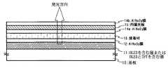
図1は、本発明の発光装置の一例を簡略に示した図である。
【0043】
まず、基板10を用意し、基板10上にOLEDを含む層またはOLEDとTFTを含む層11を形成する。基板10としては、特に限定されず、ガラス基板、石英基板、セラミック基板、シリコン基板、金属基板またはステンレス基板を用いても良い。ここでは簡略化のため、詳細なOLEDの構成やTFTの構成は図示しない。
【0044】
次いで、OLEDを含む層またはOLEDとTFTを含む層11を覆う保護膜(パッシベーション膜とも呼ばれる)を形成する。保護膜としては、AlNXOYで示される層、AlXNYで示される層、またはAl2O3で示される層から選ばれた単層または積層を用いればよく、ここではAlNXOY膜を用いる。
【0045】
そして、AlNXOYで示される層、AlXNYで示される層、またはAl2O3で示される層から選ばれた単層または積層が一方の面または双方の面に設けられた円偏光板15を用意する。ここでは双方の面にAlNXOY膜14a、14bが設けられた円偏光板15を図示している。
【0046】
次いで、OLEDを含む層またはOLEDとTFTを含む層11が形成された基板10と、双方の面にAlNXOY膜14a、14bが設けられた円偏光板15とを接着材13で貼り合わせ、封止する。接着材13としては透光性の高いもの、例えばエポキシ樹脂などを用いればよい。
【0047】
こうして、図1に示す発光装置が形成される。図1に示す発光装置は、図1中に示した矢印方向に発光するものであり、円偏光板15により背景が映り込むことを防止している。なお、本発明は、図1中に示した矢印方向に発光するものに限定されず、図1とは逆方向に発光するものにも適用できる。図1とは逆方向に発光する場合、基板10には透光性を有する基板を用い、OLEDを含む層またはOLEDとTFTを含む層11が設けられていない基板10の面側にAlNXOY膜が設けられた円偏光板を接着すればよい。
【0048】
また、膜厚100nmにおけるAlNXOY膜の透過率を図12に示す。図12に示すように、AlNXOY膜は透光性が非常に高く(可視光領域で透過率80%〜90%)、発光素子からの発光の妨げにならない。
【0049】
本発明において、AlNXOY膜は、スパッタ法を用い、例えば、窒化アルミニウム(AlN)ターゲットを用い、アルゴンガスと窒素ガスと酸素ガスを混合した雰囲気下にて成膜する。AlNXOY膜は、窒素を数atm%以上、好ましくは2.5atm%〜47.5atm%含む範囲であればよく、スパッタ条件(基板温度、原料ガスおよびその流量、成膜圧力など)を適宜調節することによって窒素濃度を調節することができる。なお、得られたAlNXOY膜のESCA(Electron Spectroscopy for Analysis)での分析による組成を図13に示す。また、アルミニウム(Al)ターゲットを用い、窒素ガス及び酸素ガスを含む雰囲気下にて成膜してもよい。なお、スパッタ法に限定されず、蒸着法やその他の公知技術を用いてもよい。
【0050】
また、AlNXOY膜による水分や酸素のブロッキング効果を確認するため、膜厚200nmのAlNXOY膜が設けられたフィルム基板でOLEDを封止したサンプルと、膜厚200nmのSiN膜が設けられたフィルム基板でOLEDを封止したサンプルとを用意して、85度に加熱した水蒸気雰囲気中での経時変化を調べる実験を行ったところ、SiN膜のサンプルに比べ、AlNXOY膜のサンプルのほうがOLEDの寿命が長く、長時間の発光が可能であった。この実験結果から、AlNXOY膜は、SiN膜よりも装置外から水分や酸素などの不純物といった有機化合物層の劣化を促す物質が侵入することを防げる材料膜であることが読み取れる。
【0051】
また、AlNXOY膜によるアルカリ金属のブロッキング効果を確認するため、シリコン基板上に膜厚50nmの熱酸化膜を設け、その上に膜厚40nmのAlNXOY膜を設け、その上にLiを含むアルミニウム電極を設け、これらの膜が設けられた面とは反対側のシリコン基板面にSiを含むアルミニウム電極を設けて300℃、1時間の熱処理を行った後、BTストレス試験(±1.7MV/cm、150℃、1時間)を行いMOS特性(C−V特性)を測定した。得られたC―V特性は、プラスの電圧を印加した時、即ち+BTの時、プラス側にシフトしていることから、シフトした原因はLiではなく、AlNXOY膜によるアルカリ金属のブロッキング効果が有ることが確認できた。比較のため、MOSの上方に絶縁膜(膜厚100nmの窒化シリコン膜)を介してAlLi合金を形成し、同様にそのMOSの特性変動を調べた。プラスの電圧を印加した時、即ち+BTの時、C−V特性変動は大きくマイナス側にシフトしており、その原因は、主にLiが活性層へ混入したことであると考えられる。
【0052】
(実施の形態2)
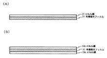
図2(A)および図2(B)は、本発明の有機偏光フィルムの一例を簡略に示した図である。
【0053】
本発明は、一方の面にAlNXOYで示される層、AlXNYで示される層、またはAl2O3で示される層から選ばれた単層または積層を有する有機偏光フィルムも発明の一つであり、図2(A)では、AlNXOY膜22が一方の面に設けられた有機偏光フィルム21を示す図である。
【0054】
また、本発明は、双方の面にAlNXOYで示される層、AlXNYで示される層、またはAl2O3で示される層から選ばれた単層または積層を有する有機偏光フィルムも発明の一つであり、図2(B)では、AlNXOY膜24a、24bが双方の面に設けられた有機偏光フィルム23を示す図である。
【0055】
ここでの有機偏光フィルムとは、偏光フィルム、位相差フィルム、またはこれらのフィルムを組み合わせたものを指しており、具体的にはポリマーフィルムの単層または積層を指している。本発明に用いられる有機偏光フィルムとしては、ポリビニルアルコール系フィルム、エチレンビニルアルコール系フィルム、セルロース系フィルム、ポリカーボネート系フィルムなどが挙げられる。
【0056】
有機偏光フィルムの一方の面または双方の面にAlNXOYで示される層、AlXNYで示される層、またはAl2O3で示される層から選ばれた単層または積層を設けることによって、アルカリ金属やアルカリ土類金属などの不純物の混入を効果的に防ぐ機能を備えたフィルムとすることができる。中でも、AlNXOYで示される層、AlXNYで示される層を用いた場合、発熱を拡散させる効果とともに、有機偏光フィルムの変形や変質を保護する効果を有する。
【0057】
図12に示したように、AlNXOY膜は透光性が非常に高く(可視光領域で透過率80%〜90%)、有機偏光フィルムの偏光機能の妨げにならない。
【0058】
こうして得られる有機偏光フィルムは、電子卓上計算機、電子時計、ワープロ、自動車や機械類の計器類等の液晶表示装置、サングラス、防目メガネ、立体メガネ、表示素子(CRT、LCD等)の反射防止フィルムとして用いることができる。
【0059】
特に、OLEDを有する発光装置に対して、背景が映り込むことを防止する反射防止手段として用いれば、酸素や水分がOLEDの有機発光層に入り込むのを防ぐこともできるため、非常に有用である。
【0060】
以上の構成でなる本発明について、以下に示す実施例でもってさらに詳細な説明を行うこととする。
【0061】
(実施例)
[実施例1]
本発明の実施例を図3及び図4を用いて説明する。ここでは、まず、同一基板上にnチャネル型TFTとpチャネル型TFTとを相補的に組み合わせたCMOS回路を同時に作製する方法について詳細に説明する。
【0062】
まず、基板100上に第1の材料層101、第2の材料層102、下地絶縁膜103を形成し、結晶構造を有する半導体膜を得た後、所望の形状にエッチング処理して島状に分離された半導体層104、105を形成する。
【0063】
基板100としては、ガラス基板(#1737)を用いる。
【0064】
また、第1の材料層101としては、成膜後或いは剥離直前において、1〜1×10¹⁰(Dyne/cm2)の範囲で引張応力を有することを特徴としている。前記第1の材料層としては、上記範囲の引張応力を有する材料であれば、特に限定されず、金属材料(Ti、Al、Ta、W、Mo、Cu、Cr、Nd、Fe、Ni、Co、Zr、Zn、Ru、Rh、Pd、Os、Ir、Ptなど)、半導体材料(例えばSi、Geなど)、絶縁体材料、有機材料のいずれか一層、またはこれらの積層を用いることができる。なかでも、タングステン膜、窒化タングステン膜、窒化チタン膜が好ましい。なお、1〜1×1010(Dyne/cm2)よりも大きな引張応力を有する膜は、熱処理を加えた場合、ピーリングを起しやすい。ここではスパッタ法で膜厚100nmの窒化チタン膜を用いる。なお、基板100と密着性が悪い場合にはバッファ層を設ければよい。
【0065】
また、第2の材料層102としては、−1〜−1×10¹⁰(Dyne/cm2)の範囲で圧縮応力を有することを特徴としている。前記第2の材料層としては、上記範囲の圧縮応力を有する材料であれば、特に限定されず、金属材料(Ti、Al、Ta、W、Mo、Cu、Cr、Nd、Fe、Ni、Co、Zr、Zn、Ru、Rh、Pd、Os、Ir、Ptなど)、半導体材料(例えばSi、Geなど)、絶縁体材料、有機材料のいずれか一層、またはこれらの積層を用いることができる。なお、−1×1010(Dyne/cm2)よりも大きな圧縮応力を有する膜は、熱処理を加えた場合、ピーリングを起しやすい。中でも、酸化シリコン材料または酸化金属材料からなる単層、またはこれらの積層が好ましい。ここではスパッタ法で膜厚200nmの酸化シリコン膜を用いる。この第1の材料層101と第2の材料層102の結合力は熱処理には強く、膜剥がれ(ピーリングとも呼ばれる)などが生じないが、物理的手段で簡単に第2の材料層の層内、あるいは界面において剥離することができる。
【0066】
また、下地絶縁膜103としては、プラズマCVD法で成膜温度400℃、原料ガスSiH4、NH3、N2Oから作製される酸化窒化シリコン膜(組成比Si=32%、O=27%、N=24%、H=17%)を50nm(好ましくは10〜200nm)形成する。次いで、表面をオゾン水で洗浄した後、表面の酸化膜を希フッ酸(1/100希釈)で除去する。次いでプラズマCVD法で成膜温度400℃、原料ガスSiH4、N2Oから作製される酸化窒化シリコン膜(組成比Si=32%、O=59%、N=7%、H=2%)を100nm(好ましくは50〜200nm)の厚さに積層形成し、さらに大気解放せずにプラズマCVD法で成膜温度300℃、成膜ガスSiH4で非晶質構造を有する半導体膜(ここではアモルファスシリコン膜)を54nmの厚さ(好ましくは25〜80nm)で形成する。
【0067】
本実施例では下地膜103を2層構造として示したが、前記絶縁膜の単層膜または2層以上積層させた構造として形成しても良い。また、半導体膜の材料に限定はないが、好ましくはシリコンまたはシリコンゲルマニウム(SiXGe1-X(X=0.0001〜0.02))合金などを用い、公知の手段(スパッタ法、LPCVD法、またはプラズマCVD法等)により形成すればよい。また、プラズマCVD装置は、枚葉式の装置でもよいし、バッチ式の装置でもよい。また、同一の成膜室で大気に触れることなく下地絶縁膜と半導体膜とを連続成膜してもよい。
【0068】
次いで、非晶質構造を有する半導体膜の表面を洗浄した後、オゾン水で表面に約2nmの極薄い酸化膜を形成する。
【0069】
次いで、重量換算で10ppmのニッケルを含む酢酸ニッケル塩溶液をスピナーで塗布する。塗布に代えてスパッタ法でニッケル元素を全面に散布する方法を用いてもよい。
【0070】
次いで、加熱処理を行い結晶化させて結晶構造を有する半導体膜を形成する。この加熱処理は、電気炉の熱処理または強光の照射を用いればよい。電気炉の熱処理で行う場合は、500℃〜650℃で4〜24時間で行えばよい。ここでは脱水素化のための熱処理(500℃、1時間)の後、結晶化のための熱処理(550℃、4時間)を行って結晶構造を有するシリコン膜を得る。なお、ここでは炉を用いた熱処理を用いて結晶化を行ったが、ランプアニール装置で結晶化を行ってもよい。なお、ここではシリコンの結晶化を助長する金属元素としてニッケルを用いた結晶化技術を用いたが、他の公知の結晶化技術、例えば固相成長法やレーザー結晶化法を用いてもよい。
【0071】
次いで、結晶構造を有するシリコン膜表面の酸化膜を希フッ酸等で除去した後、結晶化率を高め、結晶粒内に残される欠陥を補修するための第1のレーザー光(XeCl:波長308nm)の照射を大気中、または酸素雰囲気中で行う。レーザー光には波長400nm以下のエキシマレーザ光や、YAGレーザやYVO4レーザの第2高調波、第3高調波を用いる。第1のレーザー光は、パルス発振であってもよいし、連続発振でもよい。パルス発振の場合、繰り返し周波数10〜1000Hz程度のパルスレーザー光を用い、当該レーザー光を光学系にて100〜500mJ/cm2に集光し、90〜95%のオーバーラップ率をもって照射し、シリコン膜表面を走査させればよい。ここでは、繰り返し周波数30Hz、エネルギー密度393mJ/cm2で第1のレーザー光の照射を大気中で行なう。なお、大気中、または酸素雰囲気中で行うため、第1のレーザー光の照射により表面に酸化膜が形成される。
【0072】
次いで、第1のレーザー光の照射により形成された酸化膜を希フッ酸で除去した後、第2のレーザー光の照射を窒素雰囲気、或いは真空中で行い、半導体膜表面を平坦化する。このレーザー光(第2のレーザー光)には波長400nm以下のエキシマレーザー光や、YAGレーザーの第2高調波、第3高調波を用いる。第2のレーザー光のエネルギー密度は、第1のレーザー光のエネルギー密度より大きくし、好ましくは30〜60mJ/cm2大きくする。ここでは、繰り返し周波数30Hz、エネルギー密度453mJ/cm2で第2のレーザー光の照射を行ない、半導体膜表面における凹凸のP―V値(Peak to Valley、高さの最大値と最小値の差分)が50nm以下となる。このP−V値は、AFM(原子間力顕微鏡)により得られる。
【0073】
また、本実施例では第2のレーザー光の照射を全面に行ったが、オフ電流の低減は、画素部のTFTに特に効果があるため、少なくとも画素部のみに選択的に照射する工程としてもよい。
【0074】
次いで、オゾン水で表面を120秒処理して合計1〜5nmの酸化膜からなるバリア層を形成する。
【0075】
次いで、バリア層上にスパッタ法にてゲッタリングサイトとなるアルゴン元素を含む非晶質シリコン膜を膜厚150nmで形成する。本実施例のスパッタ法による成膜条件は、成膜圧力を0.3Paとし、ガス(Ar)流量を50(sccm)とし、成膜パワーを3kWとし、基板温度を150℃とする。なお、上記条件での非晶質シリコン膜に含まれるアルゴン元素の原子濃度は、3×10²⁰/cm3〜6×1020/cm3、酸素の原子濃度は1×1019/cm3〜3×1019/cm3である。その後、ランプアニール装置を用いて650℃、3分の熱処理を行いゲッタリングする。
【0076】
次いで、バリア層をエッチングストッパーとして、ゲッタリングサイトであるアルゴン元素を含む非晶質シリコン膜を選択的に除去した後、バリア層を希フッ酸で選択的に除去する。なお、ゲッタリングの際、ニッケルは酸素濃度の高い領域に移動しやすい傾向があるため、酸化膜からなるバリア層をゲッタリング後に除去することが望ましい。ここではゲッタリングを行った例を示したが、特に限定されず、他のゲッタリング方法でもよい。
【0077】
次いで、得られた結晶構造を有するシリコン膜(ポリシリコン膜とも呼ばれる)の表面にオゾン水で薄い酸化膜を形成した後、レジストからなるマスクを形成し、所望の形状にエッチング処理して島状に分離された半導体層104、105を形成する。半導体層を形成した後、レジストからなるマスクを除去する。
【0078】
次いで、フッ酸を含むエッチャントで酸化膜を除去すると同時にシリコン膜の表面を洗浄した後、ゲート絶縁膜106となる珪素を主成分とする絶縁膜を形成する。本実施例では、プラズマCVD法により115nmの厚さで酸化窒化シリコン膜(組成比Si=32%、O=59%、N=7%、H=2%)で形成する。
【0079】
次いで、図3(B)に示すように、ゲート絶縁膜106上に膜厚20〜100nmの第1の導電膜107と、膜厚100〜400nmの第2の導電膜108とを積層形成する。本実施例では、ゲート絶縁膜106上に膜厚50nmの窒化タンタル膜、膜厚370nmのタングステン膜を順次積層する。
【0080】
第1の導電膜及び第2の導電膜を形成する導電性材料としてはTa、W、Ti、Mo、Al、Cuから選ばれた元素、または前記元素を主成分とする合金材料もしくは化合物材料で形成する。また、第1の導電膜及び第2の導電膜としてリン等の不純物元素をドーピングした多結晶シリコン膜に代表される半導体膜や、、AgPdCu合金を用いてもよい。また、2層構造に限定されず、例えば、膜厚50nmのタングステン膜、膜厚500nmのアルミニウムとシリコンの合金(Al−Si)膜、膜厚30nmの窒化チタン膜を順次積層した3層構造としてもよい。また、3層構造とする場合、第1の導電膜のタングステンに代えて窒化タングステンを用いてもよいし、第2の導電膜のアルミニウムとシリコンの合金(Al−Si)膜に代えてアルミニウムとチタンの合金膜(Al−Ti)を用いてもよいし、第3の導電膜の窒化チタン膜に代えてチタン膜を用いてもよい。また、単層構造であってもよい。
【0081】
次に、図3(C)に示すように光露光工程によりレジストからなるマスク109を形成し、ゲート電極及び配線を形成するための第1のエッチング処理を行う。エッチングにはICP(Inductively Coupled Plasma:誘導結合型プラズマ)エッチング法を用いると良い。ICPエッチング法を用い、エッチング条件(コイル型の電極に印加される電力量、基板側の電極に印加される電力量、基板側の電極温度等)を適宜調節することによって所望のテーパー形状に膜をエッチングすることができる。なお、エッチング用ガスとしては、Cl2、BCl3、SiCl4、CCl4などを代表とする塩素系ガスまたはCF4、SF6、NF3などを代表とするフッ素系ガス、またはO2を適宜用いることができる。
【0082】
第1のエッチング処理では、レジストによるマスクの形状と、基板側に印加するバイアス電圧の効果により端部をテーパー形状とすることができる。テーパー部の角度は15〜45°となるようにする。また、ゲート絶縁膜上に残渣を残すことなくエッチングするためには、10〜20%程度の割合でエッチング時間を増加させると良い。W膜に対する酸化窒化シリコン膜の選択比は2〜4(代表的には3)であるので、オーバーエッチング処理により、酸化窒化シリコン膜が露出した面は20〜50nm程度エッチングされる。こうして、第1のエッチング処理により第1導電膜と第2導電膜から成る第1形状の導電層110、111(第1の導電層110a、111aと第2導電層110b、111b)を形成する。112はゲート絶縁膜であり、第1の形状の導電層で覆われない領域は20〜50nm程度エッチングされ薄くなる。
【0083】
そして、第1のドーピング処理を行いn型の不純物(ドナー)をドーピングする。(図3(D))その方法はイオンドープ法若しくはイオン注入法で行う。イオンドープ法の条件はドーズ量を1×10¹³〜5×10¹⁴/cm2として行う。n型を付与する不純物元素として15族に属する元素、典型的にはリン(P)または砒素(As)を用いる。この場合、第1形状の導電層110、111はドーピングする元素に対してマスクとなり、加速電圧を適宣調節(例えば、20〜60keV)して、ゲート絶縁膜112を通過した不純物元素により不純物領域(n+領域)113、114を形成する。例えば、不純物領域(n+領域)におけるリン(P)濃度は1×1020〜1×1021/cm3の範囲となるようにする。
【0084】
次いで、図4(A)に示すように第2のドーピング処理を行う。第1のドーピング処理よりもドーズ量を下げ高加速電圧の条件でn型の不純物(ドナー)をドーピングする。例えば、加速電圧を70〜120keVとし、1×10¹³/cm2のドーズ量で行い、図3(D)で半導体層に形成された第1の不純物領域の内側に不純物領域を形成する。ドーピングは、第2の導電膜110b、111bを不純物元素に対するマスクとして用い、第1の導電膜110a、111aの下側の領域に不純物元素が添加されるようにドーピングする。こうして、第1の導電膜110a、111aと重なる不純物領域(n−領域)115、116が形成される。この不純物領域は、第2の導電層110a、111aがほぼ同じ膜厚で残存していることから、第2の導電層に沿った方向における濃度差は小さく、1×1017〜1×1019/cm3の濃度で形成する。
【0085】
次いで、図4(B)に示すように第2のエッチング処理を行う。エッチングはICPエッチング法を用い、エッチングガスにCF4とCl2とO2を混合して、1Paの圧力でコイル型の電極に500WのRF電力(13.56MHz)を供給してプラズマを生成する。基板側(試料ステージ)には50WのRF(13.56MHz)電力を投入し、第1のエッチング処理に比べ低い自己バイアス電圧を印加する。このような条件によりタングステン膜を異方性エッチングし、第1の導電層である窒化タンタル膜またはチタン膜を残存させるようにする。こうして、第2形状の導電層117、118(第1の導電膜117a、118aと第2の導電膜117b、118b)を形成する。119はゲート絶縁膜であり、第2の形状の導電層117、118で覆われない領域はさらに20〜50nm程度エッチングされて膜厚が薄くなる。
【0086】
そして、図4(C)に示すように、レジストによるマスク120を形成し、pチャネル型TFTを形成する半導体層にp型の不純物(アクセプタ)をドーピングする。典型的にはボロン(B)を用いる。不純物領域(p+領域)121、122の不純物濃度は2×10²⁰〜2×10²¹/cm3となるようにし、含有するリン濃度の1.5〜3倍のボロンを添加して導電型を反転させる。
【0087】
以上までの工程でそれぞれの半導体層に不純物領域が形成される。第2形状の導電層117、118はゲート電極となる。その後、図4(D)に示すように、窒化シリコン膜または酸化窒化シリコン膜から成る保護絶縁膜123をプラズマCVD法で形成する。そして導電型の制御を目的としてそれぞれの半導体層に添加された不純物元素を活性化する工程を行う。
【0088】
さらに、窒化シリコン膜124を形成し、水素化処理を行う。その結果、窒化シリコン膜124中の水素が半導体層中に拡散させることで水素化を達成することができる。
【0089】
次いで、層間絶縁膜125を形成する。層間絶縁膜125は、ポリイミド、アクリルなどの有機絶縁物材料で形成する。勿論、プラズマCVD法でTEOS(Tetraethyl Ortho silicate)を用いて形成される酸化シリコン膜を適用しても良いが、平坦性を高める観点からは前記有機物材料を用いることが望ましい。
【0090】
次いで、コンタクトホールを形成し、アルミニウム(Al)、チタン(Ti)、タンタル(Ta)などを用いて、ソース配線またはドレイン配線126〜128を形成する。
【0091】
以上の工程で、nチャネル型TFTとpチャネル型TFTとを相補的に組み合わせたCMOS回路を得ることができる。
【0092】
pチャネル型TFTにはチャネル形成領域130、ソース領域またはドレイン領域として機能する不純物領域121、122を有している。
【0093】
nチャネル型TFTにはチャネル形成領域131、第2形状の導電層から成るゲート電極118と重なる不純物領域116a(Gate Overlapped Drain:GOLD領域)、ゲート電極の外側に形成される不純物領域116b(LDD領域)とソース領域またはドレイン領域として機能する不純物領域119を有している。
【0094】
このようなCMOS回路は、アクティブマトリクス型の発光装置やアクティブマトリクス型の液晶表示装置における駆動回路の一部を形成することを可能とする。それ以外にも、このようなnチャネル型TFTまたはpチャネル型TFTは、画素部のトランジスタに応用することができる。
【0095】
このようなCMOS回路を組み合わせることで基本論理回路を構成したり、さらに複雑なロジック回路(信号分割回路、D/Aコンバータ、オペアンプ、γ補正回路など)をも構成することができ、さらにはメモリやマイクロプロセッサをも形成することが可能である。
【0096】
[実施例2]
ここでは、上記実施例1で得られるTFTを用いてOLEDを有する発光装置を作製した例について図5を用い、以下に説明する。
【0097】
同一の絶縁体上に画素部とそれを駆動する駆動回路を有した発光装置の例(但し封止前の状態)を図5に示す。なお、駆動回路には基本単位となるCMOS回路を示し、画素部には一つの画素を示す。このCMOS回路は実施例1に従えば得ることができる。
【0098】
図5において、200は基板、201は第1の材料層、202は第2の材料層であり、その素子形成基板上に設けられた下地絶縁層203上にはnチャネル型TFTとpチャネル型TFTからなる駆動回路204、pチャネル型TFTからなるスイッチングTFTおよびnチャネル型TFTからなる電流制御TFTとが形成されている。また、本実施例では、TFTはすべてトップゲート型TFTで形成されている。
【0099】
nチャネル型TFTおよびpチャネル型TFTの説明は実施例1を参照すれば良いので省略する。また、スイッチングTFTはソース領域およびドレイン領域の間に二つのチャネル形成領域を有した構造(ダブルゲート構造)となっているpチャネル型TFTである。なお、本実施例はダブルゲート構造に限定されることなく、チャネル形成領域が一つ形成されるシングルゲート構造もしくは三つ形成されるトリプルゲート構造であっても良い。
【0100】
また、電流制御TFTのドレイン領域206の上には第2層間絶縁膜208が設けられる前に、第1層間絶縁膜207にコンタクトホールが設けられている。これは第2層間絶縁膜208にコンタクトホールを形成する際に、エッチング工程を簡単にするためである。第2層間絶縁膜208にはドレイン領域206に到達するようにコンタクトホールが形成され、ドレイン領域206に接続された画素電極209が設けられている。画素電極209はOLEDの陰極として機能する電極であり、周期表の1族もしくは2族に属する元素を含む導電膜を用いて形成されている。本実施例では、リチウムとアルミニウムとの化合物からなる導電膜を用いる。
【0101】
次に、213は画素電極209の端部を覆うように設けられた絶縁膜であり、本明細書中ではバンクと呼ぶ。バンク213は珪素を含む絶縁膜もしくは樹脂膜で形成すれば良い。樹脂膜を用いる場合、樹脂膜の比抵抗が1×10⁶〜1×10¹²Ωm(好ましくは1×10⁸〜1×10¹⁰Ωm)となるようにカーボン粒子もしくは金属粒子を添加すると、成膜時の絶縁破壊を抑えることができる。
【0102】
また、OLED210は画素電極(陰極)209、有機化合物層211および陽極212からなる。陽極212は、仕事関数の大きい導電膜、代表的には酸化物導電膜が用いられる。酸化物導電膜としては、酸化インジウム、酸化スズ、酸化亜鉛もしくはそれらの化合物を用いれば良い。
【0103】
なお、本明細書中では発光層に対して正孔注入層、正孔輸送層、正孔阻止層、電子輸送層、電子注入層もしくは電子阻止層を組み合わせた積層した層の総称を有機化合物層と定義する。但し、有機化合物層には有機化合物膜を単層で用いた場合も含むものとする。
【0104】
また、発光層としては、有機化合物材料であれば特に限定されないが、高分子材料や低分子材料を用いてもよく、例えばニ重項励起により発光する発光材料からなる薄膜、あるいは三重項励起により発光する発光材料からなる薄膜を用いることができる。
【0105】
なお、ここでは図示しないが陽極212を形成した後、OLED210を完全に覆うようにしてパッシベーション膜を設けることは有効である。パッシベーション膜としては、熱伝導性を有する膜、例えば、AlNXOYで示される層が適している。また、他のパッシベーション膜としては、さらにDLC膜、窒化珪素膜もしくは窒化酸化珪素膜を含む絶縁膜を積層してもよく、これらを組み合わせた積層を用いてもよい。
【0106】
次いで、OLED210を保護するため、実施の形態1に示したようにAlNXOYで示される層、AlXNYで示される層、またはAl2O3で示される層から選ばれた単層または積層を表面に有する円偏光板を貼りつけて封止(または封入)工程まで行った後、第1の材料層201が設けられた基板200を引き剥がす。そして第2の材料層にフィルム基板を接着層で貼り合わせる。貼り合わせるフィルム基板上には複数のバリア膜と、前記バリア膜どうしの間に前記バリア膜よりも応力の小さい層(応力緩和膜)とを設けることが好ましい。
【0107】
また、本実施例は、実施の形態2と組み合わせることができる。
【0108】
[実施例3]
ここでは、実施例2に示した工程とは異なる例を示し、具体的には剥離工程及び貼り合わせ工程についてさらに詳細な説明を図6、図7を用いて説明する。
【0109】
図6(A)中、300は基板、301は窒化物層、302は酸化物層、303は下地絶縁層、304a〜304cは素子、305はOLED、306は層間絶縁膜である。
【0110】
図6(A)において、基板300はガラス基板、石英基板、セラミック基板などを用いることができる。また、シリコン基板、金属基板またはステンレス基板を用いても良い。
【0111】
まず、図6(A)に示すように、実施の形態に従って、基板300上に第1の材料層301と第2の材料層302とを形成する。この第1の材料層301の膜応力と、第2の材料層302の膜応力とを異ならせることが重要である。各々の膜厚は、1nm〜1000nmの範囲で適宜設定し、各々の膜応力を調節すればよい。
【0112】
次いで、第2の材料層302上に被剥離層を形成する。被剥離層は、TFTを代表とする様々な素子(薄膜ダイオード、シリコンのPIN接合からなる光電変換素子やシリコン抵抗素子)を含む層とすればよい。また、基板300の耐え得る範囲の熱処理を行うことができる。なお、本発明において、第2の材料層302の膜応力と、第1の材料層301の膜応力が異なっていても、被剥離層の作製工程における熱処理によって膜剥がれなどが生じない。ここでは、被剥離層として、下地絶縁層303上に、駆動回路313の素子304a、304b、および画素部304の素子304cを形成し、画素部304の素子304cと電気的に接続するOLED305を形成し、OLEDを覆うように膜厚10nm〜1000nmである層間絶縁膜(透光性を有する有機樹脂)306を形成する。(図6(A))
【0113】
また、第1の材料層301や第2の材料層302によって表面に凹凸が形成された場合、下地絶縁層を形成する前後に表面を平坦化してもよい。平坦化を行った方が、被剥離層においてカバレッジが良好となり、素子を含む被剥離層を形成する場合、素子特性が安定しやすいため好ましい。なお、この平坦化処理として、塗布膜(レジスト膜等)を形成した後エッチングなどを行って平坦化するエッチバック法や機械的化学的研磨法(CMP法)等を用いればよい。
【0114】
次いで、層間絶縁膜306上に膜厚10nm〜1000nmであるAlNXOY膜で示されるアルミニウムを含む窒化酸化物膜307を形成する。(図6(B))このAlNXOY膜307は保護膜として機能する。ここでは、窒化アルミニウム(AlN)ターゲットを用い、アルゴンガス(20sccm)と窒素ガス(15sccm)と酸素ガス(5sccm)を混合した雰囲気下にて成膜する。また、アルミニウム(Al)ターゲットを用い、窒素ガス及び酸素ガスを含む雰囲気下にて成膜してもよい。また、AlNXOY膜307は、装置外から水分や酸素などの不純物といったOLEDの劣化を促す物質が侵入することを防ぐ効果も有している。
【0115】
次いで、FPC310やICチップ(図示しない)をCOG(chip on glass)方式やTAB(tape automated bonding)方式やワイヤボンディング方法で貼り付ける。また、各TFT素子の各配線と入出力端子311は、配線(接続配線)で繋がれており、入出力端子311にはFPC310を異方性導電材で接着する。異方性導電材は樹脂と表面にAuなどがメッキされた数十〜数百μm径の導電性粒子から成り、導電性粒子により入出力端子とFPCに形成された配線とが電気的に接続される。メモリ、CPU、コントローラ、D/Aコンバータ等を備えたICチップも同様に異方性導電材で基板に接着し、樹脂中に混入された導電性粒子により、ICチップに設けられた入出力端子と引出線または接続配線及び入出力端子と電気的に接続する。
【0116】
次いで、基板300を物理的手段により引き剥がすために被剥離層を固定する支持体(AlNXOY膜309bが設けられた円偏光板309a)309をエポキシ樹脂などの接着層308で貼りつける。(図6(C))また、円偏光板309aは、バリア膜として機能するAlNXOY膜を設けられて、水分や酸素などの不純物が有機発光層に入り込むのを効果的に防ぐことができる。
【0117】
FPC310やICチップを覆って支持体309を貼り付けるため、支持体309の接着により、入出力端子311とFPCとの接続をさらに固定することができる。また、ここではFPCやICチップを接着した後に支持体を接着した例を示したが、支持体を接着した後、FPCやICチップを装着してもよい。
【0118】
次いで、第1の材料層301が設けられている基板300を物理的手段により引き剥がす。第2の材料層302の膜応力と、第1の材料層301の膜応力が異なっているため、比較的小さな力で引き剥がすことができる。第1の材料層301と第2の材料層302との結合力は、熱エネルギーには耐え得る強さを有している一方、互いの膜応力は異なり、第1の材料層301と第2の材料層302との間には応力歪みを有しているため、力学的エネルギーに弱く、剥離するには最適である。こうして、第2の材料層302上に形成された被剥離層を基板300から分離することができる。剥離後の状態を図7(A)に示す。なお、この剥離方法は、小さな面積を有する被剥離層の剥離だけでなく、大きな面積を有する被剥離層を全面に渡って歩留まりよく剥離することが可能である。
【0119】
次いで、第2の材料層302をエポキシ樹脂などの接着層308により転写体309aに貼り付ける。本実施例では保護膜307に接着層を接着した例を示す。
【0120】
また、ここでは、転写体309aをプラスチックフィルム基板とすることで、軽量化を図っている。また、転写体312a上にバリア膜として機能するAlNXOYで示される層(AlNXOY膜とも呼ぶ)312bと、応力緩和膜(有機樹脂)312cと、AlNXOY膜312dとの積層を設けて、バリア膜で水分や酸素などの不純物が有機発光層に入り込むのを効果的に防ぐとともに、複数のバリア膜の間に応力緩和膜を設けることによって、よりフレキシブルな発光装置になり、曲げたときのクラックを防ぐことができる。
【0121】
このようにしてフレキシブルなプラスチック基板上に形成されたOLEDを有する発光装置が完成する。
【0122】
なお、本明細書中において、転写体とは、剥離された後、被剥離層と接着させるものであり、特に限定されず、プラスチック、ガラス、金属、セラミックス等、いかなる組成の基材でもよい。また、転写体の形状は特に限定されず、平面を有するもの、曲面を有するもの、可曲性を有するもの、フィルム状のものであってもよい。また、軽量化を最優先するのであれば、フィルム状のプラスチック基板、例えば、ポリエチレンテレフタレート(PET)、ポリエーテルスルホン(PES)、ポリエチレンナフタレート(PEN)、ポリカーボネート(PC)、ナイロン、ポリエーテルエーテルケトン(PEEK)、ポリスルホン(PSF)、ポリエーテルイミド(PEI)、ポリアリレート(PAR)、ポリブチレンテレフタレート(PBT)などのプラスチック基板が好ましい。
【0123】
また、本実施例は、実施の形態2と組み合わせることができる。
【0124】
[実施例4]
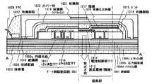
実施例3では、保護膜に接着層を接着して円偏光板を密着させる例を示したが、本実施例では、円偏光板と保護膜との間に空隙を有する例を図8に示す。
【0125】
図8(A)は、ELモジュールを示す上面図、図8(B)は図8(A)をA−A’で切断した断面図である。図8(B)において、表面にバリア膜として機能するAlNXOYで示される層(AlNXOY膜とも呼ぶ)810bと、応力緩和膜(有機樹脂)810cと、AlNXOY膜810dとの積層が設けられた可撓性を有するフィルム基板810a(例えば、プラスチック基板等)が接着層833で絶縁膜811と接着されている。なお、接着層833もバリア膜よりも応力の小さい材料を用いて応力緩和膜として機能させてもよい。このように、複数のバリア膜810b、810dを積層することで、バリア膜にクラックが生じても、他のバリア膜で水分や酸素などの不純物が有機発光層に入り込むのを効果的に防ぐことができる。加えて、複数のバリア膜の間に応力緩和膜を設けることによって、よりフレキシブルな発光装置になり、曲げたときのクラックを防ぐことができる。
【0126】
なお、ここでは耐熱性を有する基板上に絶縁膜811、絶縁膜820を設け、その上に画素部812、ソース側駆動回路814、及びゲート側駆動回路813を設けた後、カバー材、ここでは円偏光板830aを接着して固定し、耐熱性を有する基板を剥離した後、上記フィルム基板を貼りつけているが、特に限定されず、画素部822、ソース側駆動回路814、及びゲート側駆動回路813の形成温度に耐え得るフィルム基板であれば、フィルム基板上に画素部812、ソース側駆動回路814、及びゲート側駆動回路813を形成すればよく、その場合、接着層を設ける必要はない。
【0127】
耐熱性を有する基板(ガラス基板や石英基板)を剥離する技術は特に限定されず、ここでは、膜の内部応力を利用して剥離を行う剥離方法、具体的には、耐熱性を有する基板上に熱処理によって膜剥がれ(ピーリング)などのプロセス上の異常は生じない第1の材料層と第2の材料層との積層を設け、該積層上に素子(TFTや発光素子)を形成した後、物理的手段、代表的には機械的な力を加えること、例えば人間の手で引き剥がすことで容易に第2の材料層の層内または界面において、きれいに分離できる方法を用いる。第1の材料層と第2の材料層との結合力は、熱エネルギーには耐え得る強さを有している一方、剥離する直前において、引張応力を有する第1の材料層と圧縮応力を有する第2の材料層との間には応力歪みを有しているため、力学的エネルギーに弱く、剥離する。ここでは、第1の材料層としてタングステン膜を用い、第2の材料層としてスパッタ法による酸化珪素膜を用いて剥離させたため、絶縁膜811が第2の材料層に相当している。
【0128】
また、耐熱性を有する基板を剥離する他の技術として、分離層を介して存在する被剥離層を前記基板から剥離する剥離方法(特開平10−125929号公報、特開平10−125931号公報)を用いてもよい。上記公報に記載の技術は、非晶質シリコン(またはポリシリコン)からなる分離層を設け、基板を通過させてレーザー光を照射して非晶質シリコンに含まれる水素を放出させることにより、空隙を生じさせて基板を分離させるというものである。
【0129】
図8(B)において、絶縁膜820上には画素部812、ゲート側駆動回路813が形成されており、画素部812は電流制御用TFT821とそのドレインに電気的に接続された画素電極(陰極)822を含む複数の画素により形成される。電流制御用TFT821としてはpチャネル型TFTを用いることも可能であるが、nチャネル型TFTを用いることが好ましい。また、ゲート側駆動回路813はnチャネル型TFT823とpチャネル型TFT824とを組み合わせたCMOS回路を用いて形成される。各TFTの活性層としては、結晶構造を有する半導体膜(ポリシリコン膜)や非晶質構造を有する半導体膜(アモルファスシリコン膜など)を用いる。
【0130】
また、画素電極822は発光素子(OLED)の陰極として機能する。また、画素電極822の両端にはバンク825が形成され、画素電極822上には有機化合物層826および発光素子の陽極27が形成される。
【0131】
有機化合物層26としては、発光層、電荷輸送層または電荷注入層を自由に組み合わせて有機化合物層(発光及びそのためのキャリアの移動を行わせるための層)を形成すれば良い。例えば、低分子系有機化合物材料や高分子系有機化合物材料を用いればよい。また、有機化合物層826として一重項励起により発光(蛍光)する発光材料(シングレット化合物)からなる薄膜、または三重項励起により発光(リン光)する発光材料(トリプレット化合物)からなる薄膜を用いることができる。また、電荷輸送層や電荷注入層として炭化珪素等の無機材料を用いることも可能である。これらの有機材料や無機材料は公知の材料を用いることができる。
【0132】
陽極827は全画素に共通の配線としても機能し、接続配線818を経由してFPC819に電気的に接続されている。さらに、画素部812及びゲート側駆動回路813に含まれる素子は全て陽極827、有機樹脂828、及び保護膜829で覆われている。
【0133】
また、図8(A)において、828は有機樹脂、829は保護膜であり、画素部812および駆動回路813、814は有機樹脂828で覆われ、その有機樹脂は保護膜(AlNXOY膜)829で覆われている。なお、有機樹脂828としては、できるだけ可視光に対して透明もしくは半透明な材料を用いるのが好ましい。また、有機樹脂828はできるだけ水分や酸素などの不純物を透過しない材料であることが望ましい。
【0134】
さらに、画素部812および駆動回路813、814は、接着剤を用いて円偏光板830aで封止されている。円偏光板830aは、支持体として剥離前に接着される。なお、支持体となる円偏光板830aを接着した後、剥離する際には配線引き出し端子の部分(接続部分)が絶縁膜820、811のみとなり機械強度が弱くなるため、剥離前にFPC819を貼りつけ、さらに有機樹脂832で固定している。
【0135】
ここで、熱や外力などによる変形に耐えるため円偏光板830aはフィルム基板810aと同じ材質のもの、例えばプラスチック材料を用いることが望ましい。なお、水分や酸素などの不純物の侵入を防ぐため、円偏光板830aには予めAlNXOY膜830bを形成する。ここでは円偏光板中を通して発光を通過させるため、単層のバリア層(AlNXOY膜830b)としたが、フィルム基板810aと同様に、複数のバリア膜と、該バリア膜どうしの間に前記バリア膜よりも応力の小さい層(応力緩和膜)を設けてもよい。その場合、応力緩和膜としては透光性の高いものを用いる。
【0136】
なお、818はソース側駆動回路814及びゲート側駆動回路813に入力される信号を伝送するための配線であり、外部入力端子となるFPC(フレキシブルプリントサーキット)819からビデオ信号やクロック信号を受け取る。なお、ここではFPCしか図示されていないが、このFPCにはプリント配線基盤(PWB)が取り付けられていても良い。本明細書におけるELモジュールには、発光素子が設けられた基板本体だけでなく、それにFPCもしくはPWBが取り付けられた状態をも含むものとする。
【0137】
以上のような構造で発光素子をAlNXOYで示されるバリア膜810b、810d及びAlNXOYで示される保護膜829で封入することにより、発光素子を外気から完全に遮断することができ、装置外から水分や酸素等による有機化合物層の酸化が主原因である劣化を促す物質が侵入することを防ぐことができる。加えて、熱伝導性を有するAlNXOY膜により発熱を発散することができる。従って、信頼性の高い発光装置を得ることができる。
【0138】
加えて、複数のバリア膜の間に応力緩和膜を設けることによって、外力が与えられても破壊することなく、フレキシブルな発光装置になる。
【0139】
なお、フィルム基板810a上に画素部812や駆動回路や発光素子が設けられている。これらの画素部や駆動回路と同一基板上に複雑な集積回路(メモリ、CPU、コントローラ、D/Aコンバータ等)を形成しても可能であるが、少ないマスク数での作製は困難である。従って、メモリ、CPU、コントローラ、D/Aコンバータ等を備えたICチップを、COG(chip on glass)方式やTAB(tape automated bonding)方式やワイヤボンディング方法で実装することが好ましい。フィルム基板810aと円偏光板830aとを接着した後、ICチップを装着してもよいし、フィルム基板810aにICチップを装着した後で円偏光板830aで封止してもよい。
【0140】
なお、ここではFPCしか図示されていないが、このFPCにはプリント配線基盤(PWB)が取り付けられていても良い。
【0141】
また、画素電極を陽極とし、有機化合物層と陰極を積層して図8とは逆方向に発光する構成としてもよい。その場合には電流制御用TFTとしてpチャネル型TFTを用いることが好ましい。
【0142】
また、本実施例は、実施の形態2と組み合わせることができる。
【0143】
[実施例5]
本実施例では、画素電極を陽極とし、有機化合物層と陰極を積層して実施例4(図8)とは逆方向に発光する構成の一例を図9に示す。なお、上面図は図8と同一であるので省略する。
【0144】
図9に示した断面構造について以下に説明する。AlNXOY膜1000bと応力緩和膜1000cと、AlNXOY膜1000dとの積層が設けられた円偏光板1000aが絶縁膜1001と接着層1023で貼り合わせられている。絶縁膜1001上には絶縁膜1010が設けられ、絶縁膜1010の上方には画素部1002、ゲート側駆動回路1003が形成されており、画素部1002は電流制御用TFT1011とそのドレインに電気的に接続された画素電極1012を含む複数の画素により形成される。電流制御用TFT1011は、nチャネル型TFTを用いることも可能であるが、pチャネル型TFTを用いることが好ましい。また、ゲート側駆動回路1003はnチャネル型TFT1013とpチャネル型TFT1014とを組み合わせたCMOS回路を用いて形成される。
【0145】
これらのTFT(1011、1013、1014を含む)は、上記実施例1のnチャネル型TFT201、上記実施例1のpチャネル型TFT202に従って作製すればよい。
【0146】
画素電極1012は発光素子(OLED)の陽極として機能する。また、画素電極1012の両端にはバンク1015が形成され、画素電極1012上には有機化合物層1016および発光素子の陰極1017が形成される。
【0147】
陰極1017は全画素に共通の配線としても機能し、接続配線1008を経由してFPC1009に電気的に接続されている。さらに、画素部1002及びゲート側駆動回路1003に含まれる素子は全て陰極1017、有機樹脂1018、及び保護膜1019で覆われている。保護膜1019として、1000bと同じAlNXOY膜を用いてもよい。また、カバー材1020と接着層で貼り合わせている。また、カバー材には凹部を設け、乾燥剤1021を設置する。
【0148】
また、カバー材1020を図9に示す凹部形状とした場合、支持体となるカバー材1020を接着した後、剥離する際には配線引き出し端子の部分が絶縁膜1010のみとなり機械強度が弱くなるため、剥離前にFPC1009を貼りつけ、さらに有機樹脂1022で固定することが望ましい。
【0149】
また、図9では、画素電極を陽極とし、有機化合物層と陰極を積層したため、発光方向は図9に示す矢印の方向となっている。
【0150】
また、ここではトップゲート型TFTを例として説明したが、TFT構造に関係なく本発明を適用することが可能であり、例えばボトムゲート型(逆スタガ型)TFTや順スタガ型TFTに適用することが可能である。
【0151】
また、本実施例は、実施の形態2と組み合わせることができる。
【0152】
[実施例6]
本発明を実施して形成されたELモジュールは様々な電子機器に用いることができる。即ち、本発明を実施することによって、それらを組み込んだ全ての電子機器が完成される。
【0153】
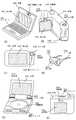
その様な電子機器としては、ビデオカメラ、デジタルカメラ、ヘッドマウントディスプレイ(ゴーグル型ディスプレイ)、カーナビゲーション、プロジェクタ、カーステレオ、パーソナルコンピュータ、携帯情報端末(モバイルコンピュータ、携帯電話または電子書籍等)などが挙げられる。それらの一例を図10、図11に示す。
【0154】
図10(A)はパーソナルコンピュータであり、本体2001、画像入力部2002、表示部2003、キーボード2004等を含む。
【0155】
図10(B)はビデオカメラであり、本体2101、表示部2102、音声入力部2103、操作スイッチ2104、バッテリー2105、受像部2106等を含む。
【0156】
図10(C)はモバイルコンピュータ(モービルコンピュータ)であり、本体2201、カメラ部2202、受像部2203、操作スイッチ2204、表示部2205等を含む。
【0157】
図10(D)はゴーグル型ディスプレイであり、本体2301、表示部2302、アーム部2303等を含む。
【0158】
図10(E)はプログラムを記録した記録媒体(以下、記録媒体と呼ぶ)を用いるプレーヤーであり、本体2401、表示部2402、スピーカ部2403、記録媒体2404、操作スイッチ2405等を含む。なお、このプレーヤーは記録媒体としてDVD(Digtial Versatile Disc)、CD等を用い、音楽鑑賞や映画鑑賞やゲームやインターネットを行うことができる。
【0159】
図10(F)はデジタルカメラであり、本体2501、表示部2502、接眼部2503、操作スイッチ2504、受像部(図示しない)等を含む。
【0160】
図11(A)は携帯電話であり、本体2901、音声出力部2902、音声入力部2903、表示部2904、操作スイッチ2905、アンテナ2906、画像入力部(CCD、イメージセンサ等)2907等を含む。
【0161】
図11(B)は携帯書籍(電子書籍)であり、本体3001、表示部3002、3003、記憶媒体3004、操作スイッチ3005、アンテナ3006等を含む。
【0162】
図11(C)はディスプレイであり、本体3101、支持台3102、表示部3103等を含む。
【0163】
ちなみに図11(C)に示すディスプレイは中小型または大型のもの、例えば5〜20インチの画面サイズのものである。また、このようなサイズの表示部を形成するためには、基板の一辺が1mのものを用い、多面取りを行って量産することが好ましい。
【0164】
以上の様に、本発明の適用範囲は極めて広く、あらゆる分野の電子機器の作製方法に適用することが可能である。また、本実施例の電子機器は実施例1〜5のどのような組み合わせからなる構成を用いても実現することができる。
【0165】
【発明の効果】
本発明により、水分や酸素やアルカリ金属やアルカリ土類金属などの不純物の拡散による劣化を抑えることが可能な発光装置を提供することができる。また、円偏光板に熱伝導性の高いバリア膜(AlNXOY膜またはAlXNYで示される層)を設けた場合、円偏光手段の機能を持たせたまま、発熱を拡散させて素子の劣化を抑える効果とともに、円偏光フィルムの変形や変質を保護する効果を有する。
【図面の簡単な説明】
【図1】 本発明の発光装置を説明する簡略断面図。
【図2】 本発明の有機偏光フィルムを説明する簡略断面図。
【図3】 TFTの作製工程を示す図。
【図4】 TFTの作製工程を示す図。
【図5】 OLEDが設けられたアクティブマトリクス基板の断面図。
【図6】 実施例3を説明する工程断面図。
【図7】 実施例3を説明する工程断面図。
【図8】 実施例4を説明するELモジュールの断面図。
【図9】 実施例5を説明するELモジュールの断面図。
【図10】 電子機器の一例を示す図。
【図11】 電子機器の一例を示す図。
【図12】 本発明のAlNXOY膜の透過率を示すグラフである。
【図13】 本発明のAlNXOY膜のESCA分析結果である。[0001]
BACKGROUND OF THE INVENTION
The present invention relates to a light emitting device, and more particularly, to a light emitting device and an electronic device having an organic light emitting device (OLED) formed on a plastic substrate. The present invention also relates to an OLED module in which an IC including a controller is mounted on the OLED panel. In this specification, the OLED panel and the OLED module are collectively referred to as a light emitting device.
[0002]
[Prior art]
In recent years, a technique for forming a thin film transistor (TFT) using a semiconductor thin film (having a thickness of about several to several hundred nm) formed on a substrate having an insulating surface has attracted attention. Thin film transistors are widely applied to electronic devices such as ICs and electro-optical devices, and development of switching devices for image display devices is urgently required.
[0003]
Various applications using such an image display device are expected, but the use for portable devices is attracting attention. Currently, many glass substrates and quartz substrates are used, but they have the disadvantage of being easily broken and heavy. Further, in mass production, it is difficult to increase the size of a glass substrate or a quartz substrate, which is not suitable. Therefore, attempts have been made to form TFT elements on a flexible substrate, typically a flexible plastic film.
[0004]
However, since the heat resistance of the plastic film is low, the maximum temperature of the process has to be lowered, and as a result, TFTs having better electrical characteristics cannot be formed when formed on a glass substrate. For this reason, a high-performance light-emitting element using a plastic film has not been realized.
[0005]
[Problems to be solved by the invention]
In recent years, research on an active matrix light-emitting device (hereinafter simply referred to as a light-emitting device) having an OLED as a self-luminous element has been activated. The light emitting device is also called an organic light emitting diode (OELD) or an organic light emitting diode (OLED).
[0006]
The OLED emits light by itself and has high visibility, is not required for a backlight necessary for a liquid crystal display device (LCD), is optimal for thinning, and has no restriction on the viewing angle. For this reason, light emitting devices using OLEDs have attracted attention as display devices that replace CRTs and LCDs.
[0007]
If a light emitting device in which an organic light emitting device (OLED) is formed on a flexible substrate such as a plastic film can be manufactured, in addition to being thin and lightweight. It can also be used for curved displays, show windows, and the like. Therefore, the application is not limited to portable devices, and the application range is very wide.
[0008]
However, a substrate made of plastic is generally easy to transmit moisture and oxygen, and deterioration of the organic light emitting layer is promoted by these materials. Therefore, the lifetime of the light emitting device is particularly likely to be shortened. Therefore, conventionally, an insulating film made of silicon nitride, silicon nitride oxide, or the like is provided between the plastic substrate and the OLED to prevent moisture and oxygen from being mixed into the organic light emitting layer. However, it has been difficult to sufficiently prevent moisture and oxygen from being mixed into the organic light emitting layer with an insulating film made of silicon nitride, silicon nitride oxide, or the like.
[0009]
In addition, a substrate such as a plastic film is generally vulnerable to heat, and if the film formation temperature of an insulating film such as silicon nitride or silicon nitride oxide is too high, the substrate is likely to be deformed. On the other hand, if the film formation temperature is too low, the film quality is deteriorated and it is difficult to sufficiently prevent the permeation of moisture and oxygen.
[0010]
Another problem is that when a device provided on a substrate such as a plastic film is driven, heat is locally generated and a part of the substrate is deformed or deteriorated.
[0011]
Further, when the thickness of an insulating film such as silicon nitride or silicon nitride oxide is increased in order to prevent moisture and oxygen from permeating, stress increases and cracks are likely to occur. Further, when the film thickness is increased, the film is likely to crack when the substrate is bent. Further, when the substrate is peeled off, the peeled layer is bent, and the peeled layer may be cracked.
[0012]
In addition to moisture and oxygen, TFT characteristics easily change when impurities of alkali metals (Li, Cs, Na, etc.), alkaline earth metals (Ca, Mg, etc.) and other metal elements diffuse into the active layer. .
[0013]
In addition, even after the final product is formed, other impurities such as human sweat and impurities from connection parts diffuse and mix in the organic light emitting layer and the active layer of the TFT, which may promote deterioration and deterioration. .
[0014]
In view of the above problems, the present invention includes a light emitting device capable of suppressing deterioration due to diffusion of impurities such as moisture, oxygen, alkali metal, and alkaline earth metal, specifically, an OLED formed on a plastic substrate. An object is to provide a light-emitting device.
[0015]
[Means for Solving the Problems]
In general, a light emitting device having an OLED is provided with a polarizing means called a circularly polarizing plate as an antireflection means for preventing a background from being reflected. Japanese Patent Application Laid-Open No. 9-127885 discloses a light emitting device in which circularly polarizing means is provided on the light exit surface.
[0016]
The present invention prevents oxygen or moisture from entering an organic light emitting layer of an OLED on one surface or both surfaces of a circularly polarizing plate provided between a light emitting element and an observer, and alkali metal and alkaline earth metal. AlN that can prevent impurities such as from entering the active layer of the TFTX OY Layer indicated by AlX NY Layer indicated by or Al2 OThree A single layer selected from the layers represented by the above or a laminate thereof (these layers are also referred to as a barrier film hereinafter) is provided. Preferably, the structure is such that oxygen and moisture are prevented from entering the organic light emitting layer of the OLED by being sandwiched between a plurality of barrier films.
[0017]
In this specification, the circular deflection plate refers to an antireflection means for preventing a background from being reflected in a light emitting device having an OLED, specifically, a retardation plate (λ / 4 plate), a retardation film. Alternatively, it refers to a circularly polarizing plate (including an elliptical polarizing plate) composed of a combination of a retardation film and a polarizing plate, a polarizing film, or a linear polarizing film. Note that reflection of the background of the observer's face or ceiling on the display unit of the light-emitting device due to reflection by a cathode or the like is called background reflection. Specifically, a circularly polarizing plate is set so that the angle formed by the polarizing axis of the polarizing plate and the polarizing axis of the retardation film is 45 °. When installed in this way, the light that has passed through the polarizing plate incident from the outside becomes linearly polarized light, twisted by 45 ° by the retardation film, becomes elliptically polarized light, and this elliptically polarized light is reflected by the cathode, and is linearly reflected by the retardation film. Become polarized. Since the angle between the linearly polarized light and the polarization axis of the polarizing plate is 90 °, the reflected light is absorbed by the polarizing plate. Therefore, a retardation film and a polarizing plate are installed in the light emitting device so that the viewer cannot see the reflection. In this way, by using the circularly polarizing plate, the light incident from the outside of the light emitting device and reflected by the cathode is prevented from coming out again. In the present specification, the circular deflection plate includes a circular deflection film.
[0018]
Further, the present invention can be applied to both a passive matrix type and an active matrix type, and the driving method is not particularly limited.
[0019]
The configuration of the invention disclosed in this specification is as follows.
A light emitting device having a light emitting element having a cathode, an organic compound layer in contact with the cathode, and an anode in contact with the organic compound layer,
In the light emitting device, AlNX OY A light-emitting device characterized in that a circularly polarizing plate having a single layer or a stack of layers represented by the above is provided.
[0020]
In the above configuration, AlN is formed on one surface or both surfaces of the circularly polarizing plate.X OY It is characterized by having a single layer or a stack of layers shown by Also, AlN on one or both sidesX OY Further reduction in weight may be achieved by using a circularly polarizing plate having a single layer or a laminate of the following as a sealing material, a support, or a cover material.
[0021]
In the above configuration, AlN is provided on one surface of the circularly polarizing plate.X OY It is characterized by having a single layer or a laminate of the layers shown in the following, and having an adhesive on the other surface. In each of the above configurations, the circularly polarizing plate is provided between the light emitting element and an observer, and is disposed between optical paths until light emitted from the light emitting element reaches the observer.
[0022]
In each of the above configurations, the AlNX OY In addition to the effect of blocking moisture and oxygen by containing 2.5 atm% to 47.5 atm% of nitrogen, the layer shown by has a feature of high heat conductivity and heat dissipation. Yes. In addition, impurities such as alkali metals and alkaline earth metals can be prevented from entering the active layer of the TFT. In each of the above configurations, the AlNX OY The film thickness of the layer indicated by is characterized by being 50 nm to 500 nm.
[0023]
Further, the light emitting device may be sandwiched between a pair of substrates, and the other configuration of the present invention is as follows.
A light emitting device having a light emitting element having a cathode, an organic compound layer in contact with the cathode, and an anode in contact with the organic compound layer sandwiched between a first substrate and a second substrate,
One of the first substrate and the second substrate is formed of AlN.X OY Layer indicated by AlX NY Or a layer indicated by Al2 OThree A light-emitting device characterized in that a circularly polarizing plate having a single layer or a laminate selected from the layers represented by the above is provided.
[0024]
In the above configuration, the circularly polarizing plate is fixed to one of the first substrate and the second substrate with an adhesive.
[0025]
AlNX OY Layer indicated by AlX NY Layer indicated by or Al2 OThree When a plastic substrate is used as the other substrate provided on the side (light emitting surface side) provided with the circularly polarizing plate provided with the layer shown in FIG.X OY Layer indicated by AlX NY Layer indicated by or Al2 OThree It is desirable to provide two or more barrier films each having a layer represented by the above, and further to provide a stress relaxation film containing a resin (hereinafter referred to as a stress relaxation film) between the two barrier films. Then, an OLED is formed and sealed on the three or more insulating films to form a light emitting device.
[0026]
In addition, AlNX OY Layer indicated by AlX NY Layer indicated by or Al2 OThree It is also possible to provide two or more barrier films composed of the layers indicated by the above, and further provide a stress relaxation film containing a resin (hereinafter referred to as a stress relaxation film) between the two barrier films.
[0027]
With the above configuration, that is, a laminate of a barrier film and a stress relaxation film provided on a circularly polarizing plate or a plastic substrate, it becomes more flexible and can prevent cracks when bent.
[0028]
AlN on circularly polarizing plate or plastic substrateX OY Layer indicated by AlX NY Or a layer indicated by Al2 OThree By laminating a plurality of barrier films composed of the layers indicated by the above, even if a crack occurs in the barrier film, it is possible to effectively prevent impurities such as moisture and oxygen from entering the organic light emitting layer in other barrier films. It is possible to effectively prevent impurities such as alkali metals from entering the active layer of the TFT.
[0029]
In addition, the entire stress can be relaxed by sandwiching a stress relaxation film having a smaller stress than the barrier film between the stress relaxation films. Therefore, even if the total thickness of the barrier film is the same, the barrier film with the stress relaxation film interposed therebetween is less prone to cracking due to stress, compared to a single barrier film.
[0030]
In addition, the combination of the barrier film and the stress relaxation film is AlN.X OY A layer (first barrier film) shown in FIG. 1, a layer made of an organic resin in contact with the layer, and AlN in contact with the layerX OY Or a layer made of an organic resin (first stress relaxation film) and AlN in contact with the layer.X OY And a layer composed of an organic resin in contact with the layer (second stress relaxation film) or AlNX OY A layer (first barrier film) shown in FIG. 1, a layer made of an organic resin in contact with the layer, and Al in contact with the layer2 OThree It may be laminated with a layer (second barrier film) indicated by
[0031]
AlN provided on a circularly polarizing plate or plastic substrateX OY The layer shown by the above may be provided with a concentration gradient such that a large amount of nitrogen is included on the side closer to the light emitting element, and the nitrogen decreases as the distance from the light emitting element increases. Thus, the barrier film is made of AlNX OY When the layer shown in FIG. 2 has a nitrogen concentration gradient, the total film thickness can be reduced, and the total translucency can be improved.
[0032]
In the present invention, when light emitted from the light-emitting element is allowed to pass through one of the light-emitting elements, the light-emitting element is preferably passed through a substrate provided with a circularly polarizing plate to be recognized by the user.
[0033]
In addition, when sandwiching between two substrates, the substrates are bonded to each other with an adhesive layer, but even if a barrier film is provided on both substrates, impurities such as moisture and oxygen penetrate through the adhesive layer. There is a risk of coming. Therefore, AlN is used as a passivation film (also called a protective film) that covers the light-emitting element.X OY Layer indicated by AlX NY Or a layer indicated by Al2 OThree It is preferable to use a single layer selected from the layers represented by the above or a laminate thereof and to have a structure in which the light-emitting element is wrapped with a barrier film and a passivation film. In addition, the light emitting element is covered with AlNX OY Layer indicated by AlX NY Or a layer indicated by Al2 OThree It is also possible to provide two or more passivation films composed of the layers indicated by the above, and further provide a stress relaxation film containing a resin (hereinafter referred to as a stress relaxation film) between the two passivation films. By sandwiching a stress relaxation film having a smaller stress than the passivation film between the stress relaxation films, the overall stress can be relaxed.
[0034]
In each of the above structures, the organic resin layer is made of Al.X NY It is characterized by comprising a single layer selected from materials having a stress lower than that of the layer, for example, polyimide, acrylic, polyamide, polyimide amide, benzocyclobutene, or epoxy resin, or a laminate thereof. In each of the above structures, the layer made of the organic resin includes an adhesive layer that adheres the substrate.
[0035]
In addition, the AlN in each of the above configurationsX OY Layer indicated by AlX NY In addition to the effect of suppressing the deterioration of the element by diffusing the heat generation of the element, the layer shown by the above has the effect of protecting the plastic substrate from deformation and alteration.
[0036]
Moreover, in each said structure, although the said plastic substrate will not be specifically limited if it is a plastic substrate which has flexibility, For example, a polyethylene terephthalate (PET), a polyether sulfone (PES), a polyethylene naphthalate (PEN), a polycarbonate It is a plastic substrate selected from (PC), nylon, polyetheretherketone (PEEK), polysulfone (PSF), polyetherimide (PEI), polyarylate (PAR), polybutylene terephthalate (PBT), and polyimide.
[0037]
In addition, other configurations of the present invention are:
AlN on the film surfaceX OY Layer indicated by AlX NY Or a layer indicated by Al2 OThree The organic polarizing film which has the single layer chosen from the layer shown by these, or those lamination | stacking.
[0038]
In the above configuration, the AlNX OY Layer indicated by AlX NY Or a layer indicated by Al2 OThree The total film thickness of the single layer selected from the layer shown by these or those laminated | stacked is 50 nm-500 nm.
[0039]
In this specification, all layers formed between the anode and the cathode of the OLED are defined as organic light emitting layers. Specifically, the organic light emitting layer includes a light emitting layer, a hole injection layer, an electron injection layer, a hole transport layer, an electron transport layer, and the like. Basically, the OLED has a structure in which an anode / light emitting layer / cathode is laminated in this order. In addition to this structure, the anode / hole injection layer / light emitting layer / cathode and the anode / hole injection layer / The light emitting layer / electron transport layer / cathode may be stacked in this order.
[0040]
In addition, the OLED has a layer containing an organic compound (organic light emitting material) from which luminescence generated by applying an electric field is obtained (hereinafter referred to as an organic light emitting layer), an anode, and a cathode. . Luminescence in organic compounds includes light emission (fluorescence) when returning from the singlet excited state to the ground state and light emission (phosphorescence) when returning from the triplet excited state to the ground state. Any one of the above-described light emission may be used, or both light emission may be used.
[0041]
DETAILED DESCRIPTION OF THE INVENTION
Embodiments of the present invention will be described below.
[0042]
(Embodiment 1)
FIG. 1 is a diagram schematically illustrating an example of a light emitting device according to the present invention.
[0043]
First, a
[0044]
Next, a protective film (also referred to as a passivation film) that covers the layer including the OLED or the layer 11 including the OLED and the TFT is formed. As the protective film, AlNX OY Layer indicated by AlX NY Or a layer indicated by Al2 OThree A single layer or a stack selected from the layers shown in FIG.X OY Use a membrane.
[0045]
And AlNX OY Layer indicated by AlX NY Or a layer indicated by Al2 OThree A circularly
[0046]
Next, the
[0047]
Thus, the light emitting device shown in FIG. 1 is formed. The light-emitting device shown in FIG. 1 emits light in the direction of the arrow shown in FIG. 1, and the
[0048]
Also, AlN at a film thickness of 100 nmX OY The permeability of the membrane is shown in FIG. As shown in FIG. 12, AlNX OY The film has a very high light-transmitting property (transmittance of 80% to 90% in the visible light region) and does not hinder light emission from the light-emitting element.
[0049]
In the present invention, AlNX OY The film is formed by sputtering, for example, using an aluminum nitride (AlN) target and in an atmosphere in which argon gas, nitrogen gas, and oxygen gas are mixed. AlNX OY The film may be in a range containing nitrogen at several atm% or more, preferably 2.5 atm% to 47.5 atm%, and the sputtering conditions (substrate temperature, source gas and its flow rate, film forming pressure, etc.) should be adjusted appropriately. The nitrogen concentration can be adjusted. The obtained AlNX OY The composition of the film analyzed by ESCA (Electron Spectroscopy for Analysis) is shown in FIG. Alternatively, an aluminum (Al) target may be used to form a film in an atmosphere containing nitrogen gas and oxygen gas. Note that the present invention is not limited to the sputtering method, and a vapor deposition method or other known techniques may be used.
[0050]
AlNX OY In order to confirm the blocking effect of moisture and oxygen by the film, AlN with a film thickness of 200 nmX OY A sample in which an OLED is sealed with a film substrate provided with a film and a sample in which an OLED is sealed with a film substrate provided with a 200 nm-thickness SiN film are prepared and heated in a water vapor atmosphere heated to 85 degrees. As a result of an experiment for examining the change over time of the AlN film, it was found that the AlNX OY The film sample had a longer OLED lifetime and could emit light for a longer time. From this experimental result, AlNX OY It can be seen that the film is a material film that can prevent a substance that promotes deterioration of the organic compound layer such as impurities such as moisture and oxygen from entering from the outside of the apparatus than the SiN film.
[0051]
AlNX OY In order to confirm the blocking effect of the alkali metal by the film, a thermal oxide film having a thickness of 50 nm is provided on the silicon substrate, and an AlN film having a thickness of 40 nm is formed thereon.X OY A film was provided, an aluminum electrode containing Li was provided thereon, and an aluminum electrode containing Si was provided on the silicon substrate surface opposite to the surface on which these films were provided, and heat treatment was performed at 300 ° C. for 1 hour. Thereafter, a BT stress test (± 1.7 MV / cm, 150 ° C., 1 hour) was performed to measure MOS characteristics (CV characteristics). The obtained CV characteristic is shifted to the positive side when a positive voltage is applied, that is, when + BT, so the cause of the shift is not Li but AlN.X OY It was confirmed that there was an alkali metal blocking effect by the film. For comparison, an AlLi alloy was formed above the MOS via an insulating film (a silicon nitride film having a thickness of 100 nm), and the characteristic variation of the MOS was similarly examined. When a positive voltage is applied, that is, when + BT, the CV characteristic fluctuation is greatly shifted to the negative side, and the cause is considered to be mainly that Li is mixed into the active layer.
[0052]
(Embodiment 2)
FIG. 2 (A) and FIG. 2 (B) are diagrams schematically showing an example of the organic polarizing film of the present invention.
[0053]
The present invention has AlN on one side.X OY Layer indicated by AlX NY Or a layer indicated by Al2 OThree An organic polarizing film having a single layer or a laminate selected from the layers shown in FIG. 2 is one of the inventions. In FIG.X OY It is a figure which shows the organic polarizing film 21 in which the film | membrane 22 was provided in one surface.
[0054]
The present invention also has AlN on both sides.X OY Layer indicated by AlX NY Or a layer indicated by Al2 OThree An organic polarizing film having a single layer or a laminate selected from the layers shown in FIG. 2 is one of the inventions. In FIG.X OY It is a figure which shows the organic polarizing film 23 in which film |
[0055]
The organic polarizing film herein refers to a polarizing film, a retardation film, or a combination of these films, and specifically refers to a single layer or a laminate of polymer films. Examples of the organic polarizing film used in the present invention include a polyvinyl alcohol film, an ethylene vinyl alcohol film, a cellulose film, and a polycarbonate film.
[0056]
AlN on one or both sides of the organic polarizing filmX OY Layer indicated by AlX NY Or a layer indicated by Al2 OThree By providing a single layer or a laminate selected from the layers represented by the above, a film having a function of effectively preventing contamination of impurities such as alkali metals and alkaline earth metals can be obtained. Above all, AlNX OY Layer indicated by AlX NY When the layer shown by is used, it has the effect of diffusing heat generation and protecting the deformation and alteration of the organic polarizing film.
[0057]
As shown in FIG. 12, AlNX OY The film has very high translucency (transmittance of 80% to 90% in the visible light region) and does not hinder the polarizing function of the organic polarizing film.
[0058]
The organic polarizing film thus obtained is used to prevent reflection of electronic desk calculators, electronic watches, word processors, liquid crystal display devices such as automobile and machinery instruments, sunglasses, eyeglasses, stereoscopic glasses, and display elements (CRT, LCD, etc.) It can be used as a film.
[0059]
In particular, if it is used as an antireflection means for preventing the background from being reflected on a light emitting device having an OLED, it is very useful because it can also prevent oxygen and moisture from entering the organic light emitting layer of the OLED. .
[0060]
The present invention having the above-described configuration will be described in more detail with the following examples.
[0061]
(Example)
[Example 1]
An embodiment of the present invention will be described with reference to FIGS. Here, a method for simultaneously manufacturing a CMOS circuit in which an n-channel TFT and a p-channel TFT are complementarily combined on the same substrate will be described in detail.
[0062]
First, a
[0063]
As the
[0064]
The
[0065]
The
[0066]
In addition, as the
[0067]
Although the
[0068]
Next, after cleaning the surface of the semiconductor film having an amorphous structure, an extremely thin oxide film of about 2 nm is formed on the surface with ozone water.
[0069]
Next, a nickel acetate salt solution containing 10 ppm of nickel by weight is applied by a spinner. Instead of coating, a method of spreading nickel element over the entire surface by sputtering may be used.
[0070]
Next, heat treatment is performed for crystallization, so that a semiconductor film having a crystal structure is formed. For this heat treatment, heat treatment in an electric furnace or irradiation with strong light may be used. When the heat treatment is performed in an electric furnace, the heat treatment may be performed at 500 to 650 ° C. for 4 to 24 hours. Here, after heat treatment for dehydrogenation (500 ° C., 1 hour), heat treatment for crystallization (550 ° C., 4 hours) is performed to obtain a silicon film having a crystal structure. Note that although crystallization is performed here using heat treatment using a furnace, crystallization may be performed using a lamp annealing apparatus. Although a crystallization technique using nickel as a metal element for promoting crystallization of silicon is used here, other known crystallization techniques such as a solid phase growth method and a laser crystallization method may be used.
[0071]
Next, after removing the oxide film on the surface of the silicon film having a crystal structure with dilute hydrofluoric acid or the like, a first laser beam (XeCl: wavelength 308 nm) for increasing the crystallization rate and repairing defects left in the crystal grains ) Is performed in the air or in an oxygen atmosphere. Laser light can be excimer laser light with a wavelength of 400 nm or less, YAG laser, YVOFour The second and third harmonics of the laser are used. The first laser light may be pulsed oscillation or continuous oscillation. In the case of pulse oscillation, pulse laser light with a repetition frequency of about 10 to 1000 Hz is used, and the laser light is 100 to 500 mJ / cm in an optical system.2 And the surface of the silicon film may be scanned by irradiating with an overlap rate of 90 to 95%. Here, repetition frequency 30Hz, energy density 393mJ / cm2 Then, the first laser beam is irradiated in the atmosphere. Note that an oxide film is formed on the surface by irradiation with the first laser light because it is performed in the air or in an oxygen atmosphere.
[0072]
Next, after removing the oxide film formed by irradiation with the first laser beam with dilute hydrofluoric acid, irradiation with the second laser beam is performed in a nitrogen atmosphere or in a vacuum to flatten the surface of the semiconductor film. As this laser light (second laser light), excimer laser light having a wavelength of 400 nm or less, and second and third harmonics of a YAG laser are used. The energy density of the second laser beam is larger than the energy density of the first laser beam, preferably 30 to 60 mJ / cm.2 Enlarge. Here, repetition frequency 30Hz, energy density 453mJ / cm2 Then, the second laser beam is irradiated, and the PV value (Peak to Valley, difference between the maximum value and the minimum value) of the unevenness on the surface of the semiconductor film becomes 50 nm or less. This PV value is obtained by an AFM (atomic force microscope).
[0073]
In this embodiment, the second laser beam is irradiated on the entire surface. However, since the reduction of the off-current is particularly effective for the TFT in the pixel portion, it is possible to selectively irradiate at least the pixel portion. Good.
[0074]
Next, the surface is treated with ozone water for 120 seconds to form a barrier layer made of an oxide film having a total thickness of 1 to 5 nm.
[0075]
Next, an amorphous silicon film containing an argon element serving as a gettering site is formed with a thickness of 150 nm on the barrier layer by a sputtering method. The film formation conditions by the sputtering method of this embodiment are as follows: the film formation pressure is 0.3 Pa, the gas (Ar) flow rate is 50 (sccm), the film formation power is 3 kW, and the substrate temperature is 150 ° C. Note that the atomic concentration of the argon element contained in the amorphous silicon film under the above conditions is 3 × 10²⁰ / CmThree ~ 6 × 10²⁰ / CmThree The atomic concentration of oxygen is 1 × 10¹⁹ / CmThree ~ 3x10¹⁹ / CmThree It is. Thereafter, heat treatment is performed at 650 ° C. for 3 minutes using a lamp annealing apparatus to perform gettering.
[0076]
Next, the amorphous silicon film containing an argon element as a gettering site is selectively removed using the barrier layer as an etching stopper, and then the barrier layer is selectively removed with dilute hydrofluoric acid. Note that during gettering, nickel tends to move to a region with a high oxygen concentration, and thus it is desirable to remove the barrier layer made of an oxide film after gettering. Here, an example in which gettering is performed is shown, but there is no particular limitation, and other gettering methods may be used.
[0077]
Next, after forming a thin oxide film with ozone water on the surface of the obtained silicon film having a crystal structure (also called a polysilicon film), a mask made of resist is formed and etched into a desired shape to form an island shape. The semiconductor layers 104 and 105 separated into two are formed. After the semiconductor layer is formed, the resist mask is removed.
[0078]
Next, the oxide film is removed with an etchant containing hydrofluoric acid, and at the same time, the surface of the silicon film is washed, and then an insulating film containing silicon as a main component to be the
[0079]
Next, as illustrated in FIG. 3B, a first
[0080]
The conductive material for forming the first conductive film and the second conductive film is an element selected from Ta, W, Ti, Mo, Al, and Cu, or an alloy material or a compound material containing the element as a main component. Form. Alternatively, a semiconductor film typified by a polycrystalline silicon film doped with an impurity element such as phosphorus, or an AgPdCu alloy may be used as the first conductive film and the second conductive film. Further, the present invention is not limited to the two-layer structure. For example, a three-layer structure in which a 50 nm-thickness tungsten film, a 500 nm-thickness aluminum and silicon alloy (Al-Si) film, and a 30 nm-thickness titanium nitride film are sequentially stacked. Also good. In the case of a three-layer structure, tungsten nitride may be used instead of tungsten of the first conductive film, or aluminum instead of the aluminum and silicon alloy (Al-Si) film of the second conductive film. A titanium alloy film (Al—Ti) may be used, or a titanium film may be used instead of the titanium nitride film of the third conductive film. Moreover, a single layer structure may be sufficient.
[0081]
Next, as shown in FIG. 3C, a resist
[0082]
In the first etching process, the end can be tapered by the shape of the mask made of resist and the effect of the bias voltage applied to the substrate side. The angle of the tapered portion is set to 15 to 45 °. In order to etch without leaving a residue on the gate insulating film, it is preferable to increase the etching time at a rate of about 10 to 20%. Since the selection ratio of the silicon oxynitride film to the W film is 2 to 4 (typically 3), the surface where the silicon oxynitride film is exposed is etched by about 20 to 50 nm by the over-etching process. Thus, first-shaped conductive layers 110 and 111 (first conductive layers 110a and 111a and second conductive layers 110b and 111b) made of the first conductive film and the second conductive film are formed by the first etching process.
[0083]
Then, a first doping process is performed to dope n-type impurities (donors). (FIG. 3D) The method is performed by ion doping or ion implantation. The condition of the ion doping method is a dose of 1 × 10¹³ ~ 5x10¹⁴ / Cm2 Do as. As the impurity element imparting n-type, an element belonging to
[0084]
Next, a second doping process is performed as shown in FIG. The n-type impurity (donor) is doped under a condition of a high acceleration voltage with a lower dose than in the first doping process. For example, the acceleration voltage is 70 to 120 keV and 1 × 10¹³ / Cm2 The impurity region is formed inside the first impurity region formed in the semiconductor layer in FIG. Doping is performed using the second conductive films 110b and 111b as masks against the impurity elements so that the impurity elements are added to the lower regions of the first conductive films 110a and 111a. Thus, impurity regions (n− regions) 115 and 116 overlapping with the first conductive films 110a and 111a are formed. In this impurity region, since the second conductive layers 110a and 111a remain with substantially the same film thickness, the concentration difference in the direction along the second conductive layer is small and 1 × 10¹⁷ ~ 1x10¹⁹ / CmThree Formed at a concentration of.
[0085]
Next, a second etching process is performed as shown in FIG. The ICP etching method is used for etching, and CF is used as an etching gas.Four And Cl2 And O2 And 500 W of RF power (13.56 MHz) is supplied to the coil-type electrode at a pressure of 1 Pa to generate plasma. 50 W RF (13.56 MHz) power is applied to the substrate side (sample stage), and a lower self-bias voltage is applied than in the first etching process. Under such conditions, the tungsten film is anisotropically etched to leave the tantalum nitride film or titanium film as the first conductive layer. Thus, second shape
[0086]
Then, as shown in FIG. 4C, a resist
[0087]
Through the above steps, impurity regions are formed in the respective semiconductor layers. The second shape
[0088]
Further, a
[0089]
Next, an
[0090]
Next, contact holes are formed, and source or drain
[0091]
Through the above steps, a CMOS circuit in which an n-channel TFT and a p-channel TFT are combined in a complementary manner can be obtained.
[0092]
The p-channel TFT has a
[0093]
The n-channel TFT includes a
[0094]
Such a CMOS circuit can form part of a driver circuit in an active matrix light-emitting device or an active matrix liquid crystal display device. In addition, such an n-channel TFT or a p-channel TFT can be applied to a transistor in a pixel portion.
[0095]
By combining such CMOS circuits, basic logic circuits can be configured, and more complex logic circuits (signal division circuits, D / A converters, operational amplifiers, γ correction circuits, etc.) can be configured, and memory It is also possible to form a microprocessor.
[0096]
[Example 2]
Here, an example in which a light-emitting device having an OLED is manufactured using the TFT obtained in Example 1 will be described with reference to FIGS.
[0097]
FIG. 5 shows an example of a light-emitting device having a pixel portion and a driving circuit for driving the pixel portion on the same insulator (but a state before sealing). Note that a CMOS circuit serving as a basic unit is shown in the driver circuit, and one pixel is shown in the pixel portion. This CMOS circuit can be obtained according to the first embodiment.
[0098]
In FIG. 5,
[0099]
Description of the n-channel TFT and the p-channel TFT will be omitted because the first embodiment can be referred to. The switching TFT is a p-channel TFT having a structure (double gate structure) having two channel formation regions between a source region and a drain region. Note that this embodiment is not limited to the double gate structure, and may be a single gate structure in which one channel formation region is formed or a triple gate structure in which three channel formation regions are formed.
[0100]
In addition, a contact hole is provided in the first
[0101]
Next,
[0102]
The
[0103]
In this specification, the organic compound layer is a general term for a layer in which a hole injection layer, a hole transport layer, a hole blocking layer, an electron transport layer, an electron injection layer, or an electron blocking layer are combined with the light emitting layer. It is defined as However, the organic compound layer includes a case where the organic compound film is used as a single layer.
[0104]
The light emitting layer is not particularly limited as long as it is an organic compound material, and a high molecular material or a low molecular material may be used. For example, a thin film made of a light emitting material that emits light by doublet excitation, or triplet excitation. A thin film made of a light emitting material that emits light can be used.
[0105]
Although not shown here, it is effective to provide a passivation film so as to completely cover the
[0106]
Next, in order to protect the
[0107]
Further, this embodiment can be combined with Embodiment Mode 2.
[0108]
[Example 3]
Here, an example different from the process shown in Example 2 is shown, and specifically, a more detailed description of the peeling process and the bonding process will be described with reference to FIGS.
[0109]
In FIG. 6A, 300 is a substrate, 301 is a nitride layer, 302 is an oxide layer, 303 is a base insulating layer, 304a to 304c are elements, 305 is an OLED, and 306 is an interlayer insulating film.
[0110]
In FIG. 6A, a glass substrate, a quartz substrate, a ceramic substrate, or the like can be used as the
[0111]
First, as illustrated in FIG. 6A, a first material layer 301 and a second material layer 302 are formed over a
[0112]
Next, a layer to be peeled is formed over the second material layer 302. The layer to be peeled may be a layer including various elements typified by TFTs (thin film diodes, photoelectric conversion elements made of silicon PIN junctions, and silicon resistance elements). Further, heat treatment within a range that the
[0113]
In the case where unevenness is formed on the surface by the first material layer 301 or the second material layer 302, the surface may be planarized before and after the base insulating layer is formed. The planarization is preferable because the coverage in the layer to be peeled is good and the layer to be peeled including the element is formed because the element characteristics are easily stabilized. Note that as this planarization treatment, an etch-back method in which a coating film (resist film or the like) is formed and then planarized by etching or the like, a mechanical chemical polishing method (CMP method), or the like may be used.
[0114]
Next, AlN having a thickness of 10 nm to 1000 nm is formed on the interlayer insulating film 306.X OY A nitride oxide film 307 containing aluminum shown in the film is formed. (FIG. 6 (B)) This AlNX OY The film 307 functions as a protective film. Here, an aluminum nitride (AlN) target is used, and deposition is performed in an atmosphere in which argon gas (20 sccm), nitrogen gas (15 sccm), and oxygen gas (5 sccm) are mixed. Alternatively, an aluminum (Al) target may be used to form a film in an atmosphere containing nitrogen gas and oxygen gas. AlNX OY The film 307 also has an effect of preventing a substance that promotes the deterioration of the OLED such as moisture or oxygen from entering from outside the apparatus.
[0115]
Next, the
[0116]
Next, a support (AlN) for fixing the layer to be peeled off in order to peel off the
[0117]
Since the support body 309 is attached so as to cover the
[0118]
Next, the
[0119]
Next, the second material layer 302 is attached to the transfer body 309a with an adhesive layer 308 such as an epoxy resin. In this embodiment, an example in which an adhesive layer is bonded to the protective film 307 is shown.
[0120]
Here, the transfer body 309a is a plastic film substrate to reduce the weight. Further, AlN functions as a barrier film on the transfer body 312a.X OY Layer (AlNX OY 312b), stress relaxation film (organic resin) 312c, and AlNX OY By providing a stack with the film 312d to effectively prevent impurities such as moisture and oxygen from entering the organic light emitting layer in the barrier film, and providing a stress relaxation film between the plurality of barrier films, It becomes a light-emitting device and can prevent cracks when bent.
[0121]
In this way, a light emitting device having an OLED formed on a flexible plastic substrate is completed.
[0122]
Note that in this specification, the transfer body is to be bonded to the layer to be peeled after being peeled, and is not particularly limited, and may be a base material having any composition such as plastic, glass, metal, ceramics and the like. The shape of the transfer body is not particularly limited, and may be a flat surface, a curved surface, a bendable material, or a film. If weight reduction is the top priority, a film-like plastic substrate such as polyethylene terephthalate (PET), polyethersulfone (PES), polyethylene naphthalate (PEN), polycarbonate (PC), nylon, polyetherether Plastic substrates such as ketone (PEEK), polysulfone (PSF), polyetherimide (PEI), polyarylate (PAR), and polybutylene terephthalate (PBT) are preferable.
[0123]
Further, this embodiment can be combined with Embodiment Mode 2.
[0124]
[Example 4]
In Example 3, an example in which an adhesive layer is adhered to the protective film to attach the circularly polarizing plate was shown. However, in this example, an example in which a gap is provided between the circularly polarizing plate and the protective film is shown in FIG. .
[0125]
8A is a top view illustrating the EL module, and FIG. 8B is a cross-sectional view taken along line AA ′ of FIG. 8A. In FIG. 8B, AlN functioning as a barrier film on the surface.X OY Layer (AlNX OY 810b, stress relaxation film (organic resin) 810c, and AlNX OY A flexible film substrate 810 a (eg, a plastic substrate) provided with a stack with the film 810 d is bonded to the insulating film 811 with an adhesive layer 833. Note that the adhesive layer 833 may also function as a stress relaxation film using a material having a stress smaller than that of the barrier film. As described above, by stacking the plurality of barrier films 810b and 810d, even when a crack occurs in the barrier film, it is possible to effectively prevent impurities such as moisture and oxygen from entering the organic light emitting layer in other barrier films. Can do. In addition, by providing a stress relaxation film between the plurality of barrier films, a more flexible light-emitting device can be obtained and cracks when bent can be prevented.
[0126]
Note that here, an insulating film 811 and an insulating film 820 are provided over a heat-resistant substrate, and after the pixel portion 812, the source side driver circuit 814, and the gate side driver circuit 813 are provided, a cover material, here The film substrate is attached after the circularly polarizing plate 830a is bonded and fixed, and the substrate having heat resistance is peeled off. However, the
[0127]
The technology for peeling off a substrate having heat resistance (a glass substrate or a quartz substrate) is not particularly limited, and here, a peeling method using the internal stress of the film, specifically, on a substrate having heat resistance After providing a stack of a first material layer and a second material layer that does not cause a process abnormality such as film peeling (peeling) by heat treatment, and forming an element (TFT or light emitting element) on the stack, Use a method that can be easily separated in the layer or interface of the second material layer by applying physical means, typically mechanical force, for example, by peeling it with a human hand. The bonding force between the first material layer and the second material layer is strong enough to withstand thermal energy, while the first material layer having tensile stress and the compressive stress immediately before peeling. Since it has a stress strain between the second material layer and the second material layer, it is weak against mechanical energy and peels off. Here, the insulating film 811 corresponds to the second material layer because a tungsten film is used as the first material layer and a silicon oxide film by a sputtering method is used as the second material layer.
[0128]
Further, as another technique for peeling off a substrate having heat resistance, a peeling method for peeling off a layer to be peeled existing through a separation layer from the substrate (JP 10-125929 A, JP 10-125931 A). May be used. The technique described in the above publication provides a separation layer made of amorphous silicon (or polysilicon), passes through the substrate, and irradiates laser light to release hydrogen contained in the amorphous silicon. This causes the substrate to be separated.
[0129]
8B, a pixel portion 812 and a gate side driver circuit 813 are formed over an insulating film 820. The pixel portion 812 includes a pixel electrode (cathode) electrically connected to the
[0130]
The
[0131]
As the organic compound layer 26, an organic compound layer (a layer for emitting light and moving carriers therefor) may be formed by freely combining a light emitting layer, a charge transport layer, or a charge injection layer. For example, a low molecular organic compound material or a high molecular organic compound material may be used. As the organic compound layer 826, a thin film made of a light emitting material (singlet compound) that emits light (fluorescence) by singlet excitation or a thin film made of a light emitting material (phosphorescence) that emits light (phosphorescence) by triplet excitation can be used. it can. It is also possible to use an inorganic material such as silicon carbide for the charge transport layer or the charge injection layer. As these organic materials and inorganic materials, known materials can be used.
[0132]
The anode 827 also functions as a wiring common to all pixels, and is electrically connected to the
[0133]
In FIG. 8A, 828 is an organic resin, 829 is a protective film, the pixel portion 812 and the drive circuits 813 and 814 are covered with the organic resin 828, and the organic resin is a protective film (AlN).X OY Film) 829. Note that as the organic resin 828, a material that is as transparent or translucent as possible to visible light is preferably used. The organic resin 828 is desirably a material that does not transmit impurities such as moisture and oxygen as much as possible.
[0134]
Further, the pixel portion 812 and the drive circuits 813 and 814 are sealed with a circularly polarizing plate 830a using an adhesive. The circularly polarizing plate 830a is bonded as a support before peeling. In addition, after bonding the circularly polarizing plate 830a to be the support, when peeling off, the wiring lead-out terminal portion (connection portion) becomes only the insulating films 820 and 811 and the mechanical strength is weakened. Therefore, the
[0135]
Here, the circularly polarizing plate 830a is preferably made of the same material as the film substrate 810a, for example, a plastic material, in order to withstand deformation due to heat or external force. In order to prevent intrusion of impurities such as moisture and oxygen, the circularly polarizing plate 830a is previously provided with AlN.X OY A film 830b is formed. Here, in order to allow light emission to pass through the circularly polarizing plate, a single barrier layer (AlNX OY Although the film 830b), as in the film substrate 810a, a plurality of barrier films and a layer (stress relaxation film) having a stress smaller than that of the barrier film may be provided between the barrier films. In that case, a highly light-transmitting film is used as the stress relaxation film.
[0136]
Note that reference numeral 818 denotes a wiring for transmitting signals input to the source side driver circuit 814 and the gate side driver circuit 813, and receives a video signal and a clock signal from an FPC (flexible printed circuit) 819 serving as an external input terminal. Although only the FPC is shown here, a printed wiring board (PWB) may be attached to the FPC. The EL module in this specification includes not only a substrate body provided with a light-emitting element but also a state in which an FPC or PWB is attached thereto.
[0137]
The light emitting device having the above structure is made of AlN.X OY Barrier films 810b and 810d and AlNX OY The light-emitting element can be completely shielded from the outside air by sealing with a protective film 829 shown in FIG. 2, and a substance that promotes deterioration mainly due to oxidation of the organic compound layer by moisture, oxygen, or the like enters from the outside of the apparatus. Can be prevented. In addition, AlN with thermal conductivityX OY Heat generation can be dissipated by the film. Therefore, a highly reliable light-emitting device can be obtained.
[0138]
In addition, by providing a stress relaxation film between the plurality of barrier films, a flexible light-emitting device is obtained without being broken even when an external force is applied.
[0139]
Note that a pixel portion 812, a driving circuit, and a light-emitting element are provided over the film substrate 810a. Although it is possible to form a complicated integrated circuit (memory, CPU, controller, D / A converter, etc.) on the same substrate as these pixel portions and drive circuits, it is difficult to manufacture with a small number of masks. Therefore, it is preferable to mount an IC chip including a memory, a CPU, a controller, a D / A converter, and the like by a COG (chip on glass) method, a TAB (tape automated bonding) method, or a wire bonding method. After bonding the film substrate 810a and the circularly polarizing plate 830a, an IC chip may be mounted, or after mounting the IC chip on the film substrate 810a, sealing may be performed with the circularly polarizing plate 830a.
[0140]
Although only the FPC is shown here, a printed wiring board (PWB) may be attached to the FPC.
[0141]
Alternatively, the pixel electrode may be an anode, the organic compound layer and the cathode may be stacked, and light may be emitted in the direction opposite to that in FIG. In that case, a p-channel TFT is preferably used as the current control TFT.
[0142]
Further, this embodiment can be combined with Embodiment Mode 2.
[0143]
[Example 5]
In this embodiment, an example of a structure in which the pixel electrode is used as an anode, an organic compound layer and a cathode are stacked, and light is emitted in a direction opposite to that in Embodiment 4 (FIG. 8) is shown in FIG. The top view is the same as FIG.
[0144]
The cross-sectional structure shown in FIG. 9 will be described below. AlNX OY Film 1000b, stress relaxation film 1000c, AlNX OY A circularly polarizing plate 1000 a provided with a stack with the film 1000 d is attached to the insulating film 1001 and the adhesive layer 1023. An insulating film 1010 is provided over the insulating film 1001, and a pixel portion 1002 and a gate side driver circuit 1003 are formed above the insulating film 1010. The pixel portion 1002 is electrically connected to the
[0145]
These TFTs (including 1011, 1013, and 1014) may be manufactured according to the n-
[0146]
The pixel electrode 1012 functions as an anode of a light emitting element (OLED). A bank 1015 is formed at both ends of the pixel electrode 1012, and an organic compound layer 1016 and a cathode 1017 of a light emitting element are formed on the pixel electrode 1012.
[0147]
The cathode 1017 also functions as a wiring common to all pixels, and is electrically connected to the
[0148]
Further, when the cover material 1020 has the concave shape shown in FIG. 9, when the cover material 1020 serving as a support is bonded and then peeled off, the wiring lead-out terminal portion becomes only the insulating film 1010 and the mechanical strength is weakened. It is desirable that the
[0149]
In FIG. 9, since the pixel electrode is an anode and the organic compound layer and the cathode are stacked, the light emission direction is the direction of the arrow shown in FIG.
[0150]
Although the top gate type TFT has been described as an example here, the present invention can be applied regardless of the TFT structure. For example, it can be applied to a bottom gate type (reverse stagger type) TFT or a forward stagger type TFT. Is possible.
[0151]
Further, this embodiment can be combined with Embodiment Mode 2.
[0152]
[Example 6]
An EL module formed by implementing the present invention can be used for various electronic devices. That is, by implementing the present invention, all electronic devices incorporating them are completed.
[0153]
Such electronic devices include video cameras, digital cameras, head mounted displays (goggles type displays), car navigation systems, projectors, car stereos, personal computers, personal digital assistants (mobile computers, mobile phones, electronic books, etc.), etc. Can be mentioned. Examples of these are shown in FIGS.
[0154]
FIG. 10A illustrates a personal computer, which includes a main body 2001, an image input portion 2002, a display portion 2003, a
[0155]
FIG. 10B illustrates a video camera, which includes a main body 2101, a display portion 2102, an
[0156]
FIG. 10C illustrates a mobile computer, which includes a main body 2201, a camera unit 2202, an
[0157]
FIG. 10D illustrates a goggle type display, which includes a
[0158]
FIG. 10E shows a player using a recording medium (hereinafter referred to as a recording medium) on which a program is recorded, and includes a main body 2401, a
[0159]
FIG. 10F illustrates a digital camera, which includes a main body 2501, a
[0160]
FIG. 11A shows a cellular phone, which includes a
[0161]
FIG. 11B illustrates a portable book (electronic book), which includes a
[0162]
FIG. 11C illustrates a display, which includes a
[0163]
Incidentally, the display shown in FIG. 11C is a medium or small size display, for example, a screen size of 5 to 20 inches. Further, in order to form a display portion having such a size, it is preferable to use a substrate having a side of 1 m and perform mass production by performing multiple chamfering.
[0164]
As described above, the applicable range of the present invention is so wide that the present invention can be applied to methods for manufacturing electronic devices in various fields. Moreover, the electronic apparatus of a present Example is realizable even if it uses the structure which consists of what combination of Examples 1-5.
[0165]
【The invention's effect】
According to the present invention, a light-emitting device capable of suppressing deterioration due to diffusion of impurities such as moisture, oxygen, alkali metal, and alkaline earth metal can be provided. In addition, a barrier film with high thermal conductivity (AlNX OY Film or AlX NY In the case where the layer shown in FIG. 2 is provided, while maintaining the function of the circularly polarizing means, it has the effect of suppressing the deterioration of the element by diffusing heat generation and protecting the deformation and alteration of the circularly polarizing film.
[Brief description of the drawings]
FIG. 1 is a simplified cross-sectional view illustrating a light-emitting device of the present invention.
FIG. 2 is a simplified cross-sectional view illustrating an organic polarizing film of the present invention.
FIG. 3 is a view showing a manufacturing process of a TFT.
4A and 4B are diagrams showing a manufacturing process of a TFT.
FIG. 5 is a cross-sectional view of an active matrix substrate provided with an OLED.
6 is a process cross-sectional view illustrating Example 3. FIG.
7 is a process cross-sectional view illustrating Example 3. FIG.
FIG. 8 is a cross-sectional view of an EL module for explaining Example 4;
FIG. 9 is a cross-sectional view of an EL module for explaining Example 5;
FIG 10 illustrates an example of an electronic device.
FIG 11 illustrates an example of an electronic device.
FIG. 12: AlN of the present inventionX OY It is a graph which shows the transmittance | permeability of a film | membrane.
FIG. 13: AlN of the present inventionX OY It is an ESCA analysis result of a film.
Claims (15)
Translated fromJapanese前記基板は可撓性を有し、
AlNxOyで示される材料でなる第1の層と、前記第1の層に接する有機樹脂からなる層と、前記有機樹脂からなる層に接するAlNxOyでなる第2の層との積層膜が前記基板と前記発光素子との間に設けられ、
AlNXOYで示される材料でなる第3の層を有する円偏光板が、前記発光素子の光出射面側に設けられ、
前記第1の層、前記第2の層および前記第3の層はそれぞれ、前記発光素子との距離が近い側に窒素が多く含まれ、遠ざかるにつれ窒素の濃度が減少していることを特徴とする発光装置。On a substrate, a light emitting device having a light emitting element having a cathode, a layer containing an organic compound in contact with the cathode, and an anode in contact with the layer containing the organic compound,
The substrate has flexibility;
A first layer made of a material represented by AlNx Oy , a layer made of an organic resin in contact with the first layer, and a second layer made of AlNx Oy in contact with the layer made of the organic resin. A laminated film is provided between the substrate and the light emitting element,
A circularly polarizing plate having a third layer made of a material represented by AlNX OY is provided on the light emitting surface side of the light emitting element;
Each of the first layer, the second layer, and the third layer includes a large amount of nitrogen on the side closer to the light emitting element, and the concentration of nitrogen decreases as the distance from the light emitting element increases. Light-emitting device.
前記基板は可撓性を有し、
AlNxOyで示される材料でなる第1の層と、前記第1の層に接する有機樹脂からなる層と、前記有機樹脂からなる層に接するAlNxOyでなる第2の層との積層膜が前記基板と前記接着層との間に設けられ、
AlNXOYで示される材料でなる第3の層を有する円偏光板が、前記発光素子の光出射面側に設けられ、
前記第1の層、前記第2の層および前記第3の層はそれぞれ、前記発光素子との距離が近い側に窒素が多く含まれ、遠ざかるにつれ窒素の濃度が減少していることを特徴とする発光装置。An adhesive layer on the substrate, a layer including a transistor on the adhesive layer, a cathode, a layer including an organic compound in contact with the cathode, and an anode in contact with the layer including the organic compound on the layer including the transistor A light-emitting device comprising:
The substrate has flexibility;
A first layer made of a material represented by AlNx Oy , a layer made of an organic resin in contact with the first layer, and a second layer made of AlNx Oy in contact with the layer made of the organic resin. A laminated film is provided between the substrate and the adhesive layer;
A circularly polarizing plate having a third layer made of a material represented by AlNX OY is provided on the light emitting surface side of the light emitting element;
Each of the first layer, the second layer, and the third layer includes a large amount of nitrogen on the side closer to the light emitting element, and the concentration of nitrogen decreases as the distance from the light emitting element increases. Light-emitting device.
前記積層膜上に、陰極と、前記陰極に接する有機化合物を含む層と、前記有機化合物を含む層に接する陽極とを有する発光素子が設けられ、
前記発光素子上に、AlNXOYで示される材料でなる第3の層を有する円偏光板が設けられ、
前記第1の層、前記第2の層および前記第3の層はそれぞれ、前記発光素子との距離が近い側に窒素が多く含まれ、遠ざかるにつれ窒素の濃度が減少していることを特徴とする発光装置。A first layer made of a material represented by AlNx Oy on a flexible substrate, a layer made of an organic resin in contact with the first layer, and AlNx Oy in contact with the layer made of the organic resin A laminated film with a second layer consisting of:
A light emitting element having a cathode, a layer containing an organic compound in contact with the cathode, and an anode in contact with the layer containing the organic compound is provided on the stacked film,
On the light emitting element, a circularly polarizing plate having a third layer made of a material represented by AlNX OY is provided,
Each of the first layer, the second layer, and the third layer includes a large amount of nitrogen on the side closer to the light emitting element, and the concentration of nitrogen decreases as the distance from the light emitting element increases. Light-emitting device.
前記積層膜上に、接着層と、前記接着層上にトランジスタを含む層と、前記トランジスタを含む層上に、陰極と、前記陰極に接する有機化合物を含む層と、前記有機化合物を含む層に接する陽極とを有する発光素子とが設けられ、
前記発光素子上に、AlNXOYで示される材料でなる第3の層を有する円偏光板が設けられ、
前記第1の層、前記第2の層および前記第3の層はそれぞれ、前記発光素子との距離が近い側に窒素が多く含まれ、遠ざかるにつれ窒素の濃度が減少していることを特徴とする発光装置。A first layer made of a material represented by AlNx Oy on a flexible substrate, a layer made of an organic resin in contact with the first layer, and AlNx Oy in contact with the layer made of the organic resin A laminated film with a second layer consisting of:
On the laminated film, an adhesive layer, a layer including a transistor on the adhesive layer, a layer including the transistor, a layer including an organic compound in contact with the cathode, and a layer including the organic compound A light-emitting element having an anode in contact therewith,
On the light emitting element, a circularly polarizing plate having a third layer made of a material represented by AlNX OY is provided,
Each of the first layer, the second layer, and the third layer includes a large amount of nitrogen on the side closer to the light emitting element, and the concentration of nitrogen decreases as the distance from the light emitting element increases. Light-emitting device.
Priority Applications (3)
| Application Number | Priority Date | Filing Date | Title |
|---|---|---|---|
| JP2001305862AJP4166455B2 (en) | 2001-10-01 | 2001-10-01 | Polarizing film and light emitting device |
| US10/260,398US7005671B2 (en) | 2001-10-01 | 2002-10-01 | Light emitting device, electronic equipment, and organic polarizing film |
| US11/203,406US7800099B2 (en) | 2001-10-01 | 2005-08-15 | Light emitting device, electronic equipment, and organic polarizing film |
Applications Claiming Priority (1)
| Application Number | Priority Date | Filing Date | Title |
|---|---|---|---|
| JP2001305862AJP4166455B2 (en) | 2001-10-01 | 2001-10-01 | Polarizing film and light emitting device |
Publications (3)
| Publication Number | Publication Date |
|---|---|
| JP2003115388A JP2003115388A (en) | 2003-04-18 |
| JP2003115388A5 JP2003115388A5 (en) | 2005-06-02 |
| JP4166455B2true JP4166455B2 (en) | 2008-10-15 |
Family
ID=19125587
Family Applications (1)
| Application Number | Title | Priority Date | Filing Date |
|---|---|---|---|
| JP2001305862AExpired - Fee RelatedJP4166455B2 (en) | 2001-10-01 | 2001-10-01 | Polarizing film and light emitting device |
Country Status (2)
| Country | Link |
|---|---|
| US (2) | US7005671B2 (en) |
| JP (1) | JP4166455B2 (en) |
Families Citing this family (345)
| Publication number | Priority date | Publication date | Assignee | Title |
|---|---|---|---|---|
| JP4101511B2 (en)* | 2001-12-27 | 2008-06-18 | 株式会社半導体エネルギー研究所 | Light emitting device and manufacturing method thereof |
| US20070258085A1 (en)* | 2006-05-02 | 2007-11-08 | Robbins Michael D | Substrate illumination and inspection system |
| US7161291B2 (en)* | 2002-09-24 | 2007-01-09 | Dai Nippon Printing Co., Ltd | Display element and method for producing the same |
| AU2003275615A1 (en)* | 2002-11-01 | 2004-05-25 | Semiconductor Energy Laboratory Co., Ltd. | Semiconductor device and method for manufacturing semiconductor device |
| US6881975B2 (en)* | 2002-12-17 | 2005-04-19 | Semiconductor Energy Laboratory Co., Ltd. | Semiconductor device and method of manufacturing the same |
| US7652359B2 (en)* | 2002-12-27 | 2010-01-26 | Semiconductor Energy Laboratory Co., Ltd. | Article having display device |
| TW579610B (en)* | 2003-01-30 | 2004-03-11 | Epistar Corp | Nitride light-emitting device having adhered reflective layer |
| US7973313B2 (en) | 2003-02-24 | 2011-07-05 | Semiconductor Energy Laboratory Co., Ltd. | Thin film integrated circuit device, IC label, container comprising the thin film integrated circuit, manufacturing method of the thin film integrated circuit device, manufacturing method of the container, and management method of product having the container |
| US7592239B2 (en)* | 2003-04-30 | 2009-09-22 | Industry University Cooperation Foundation-Hanyang University | Flexible single-crystal film and method of manufacturing the same |
| US20040218133A1 (en)* | 2003-04-30 | 2004-11-04 | Park Jong-Wan | Flexible electro-optical apparatus and method for manufacturing the same |
| JP4131838B2 (en)* | 2003-05-16 | 2008-08-13 | 株式会社半導体エネルギー研究所 | Display device |
| JP4417027B2 (en)* | 2003-05-21 | 2010-02-17 | 株式会社半導体エネルギー研究所 | Light emitting device |
| JP4531475B2 (en)* | 2003-08-15 | 2010-08-25 | 株式会社半導体エネルギー研究所 | Method for manufacturing semiconductor device |
| DE10339941A1 (en)* | 2003-08-29 | 2005-03-24 | BSH Bosch und Siemens Hausgeräte GmbH | Refrigeration unit with OLED display |
| CN100433377C (en)* | 2003-09-05 | 2008-11-12 | 晶元光电股份有限公司 | Nitride light-emitting element with pasted reflection layer |
| US20050093437A1 (en)* | 2003-10-31 | 2005-05-05 | Ouyang Michael X. | OLED structures with strain relief, antireflection and barrier layers |
| KR100565636B1 (en) | 2003-12-02 | 2006-03-30 | 엘지전자 주식회사 | Organic EL element and its manufacturing method |
| US7768405B2 (en)* | 2003-12-12 | 2010-08-03 | Semiconductor Energy Laboratory Co., Ltd | Semiconductor device and manufacturing method thereof |
| KR100656497B1 (en)* | 2004-02-09 | 2006-12-11 | 삼성에스디아이 주식회사 | Organic light emitting display device and manufacturing method |
| KR100581903B1 (en)* | 2004-03-09 | 2006-05-22 | 삼성에스디아이 주식회사 | Electroluminescent display device |
| KR100699988B1 (en)* | 2004-03-19 | 2007-03-26 | 삼성에스디아이 주식회사 | Flat Panel Display |
| DE102004016627A1 (en) | 2004-03-29 | 2005-11-24 | Gottlieb Binder Gmbh & Co. Kg | display device |
| US7764012B2 (en)* | 2004-04-16 | 2010-07-27 | Semiconductor Energy Laboratory Co., Ltd | Light emitting device comprising reduced frame portion, manufacturing method with improve productivity thereof, and electronic apparatus |
| JP4637513B2 (en)* | 2004-06-25 | 2011-02-23 | 株式会社 日立ディスプレイズ | Display device and driving method thereof |
| TWI238020B (en)* | 2004-08-26 | 2005-08-11 | Ind Tech Res Inst | Fabrication and structure for pixels of top-emitting organic light emitting diode |
| US7753751B2 (en) | 2004-09-29 | 2010-07-13 | Semiconductor Energy Laboratory Co., Ltd. | Method of fabricating the display device |
| JP2006100140A (en)* | 2004-09-29 | 2006-04-13 | Toshiba Matsushita Display Technology Co Ltd | Manufacturing method of organic EL display device |
| US7733448B2 (en)* | 2004-10-29 | 2010-06-08 | Semiconductor Energy Laboratory Co., Ltd. | Liquid crystal display device |
| JP2006138983A (en)* | 2004-11-11 | 2006-06-01 | Sony Corp | Particulate structural body, particulate structural body forming method and screen |
| KR100669778B1 (en)* | 2004-11-20 | 2007-01-16 | 삼성에스디아이 주식회사 | Substrate with substrate and thin film transistor |
| US20070188506A1 (en)* | 2005-02-14 | 2007-08-16 | Lieven Hollevoet | Methods and systems for power optimized display |
| JP2007026970A (en)* | 2005-07-20 | 2007-02-01 | Hitachi Displays Ltd | Organic light emitting display |
| KR100696200B1 (en)* | 2005-10-14 | 2007-03-20 | 한국전자통신연구원 | Active Drive Display and Manufacturing Method Thereof |
| TWI398705B (en)* | 2005-11-04 | 2013-06-11 | Semiconductor Energy Lab | Display device |
| WO2007063782A1 (en)* | 2005-11-30 | 2007-06-07 | Semiconductor Energy Laboratory Co., Ltd. | Display device |
| EP1793264A1 (en)* | 2005-12-05 | 2007-06-06 | Semiconductor Energy Laboratory Co., Ltd. | Liquid crystal display device |
| KR100714016B1 (en)* | 2005-12-13 | 2007-05-04 | 삼성에스디아이 주식회사 | Organic light emitting display |
| JP2007173084A (en)* | 2005-12-22 | 2007-07-05 | Canon Inc | Light emitting element |
| WO2007072766A1 (en)* | 2005-12-22 | 2007-06-28 | Semiconductor Energy Laboratory Co., Ltd. | Display device |
| EP1804114B1 (en)* | 2005-12-28 | 2014-03-05 | Semiconductor Energy Laboratory Co., Ltd. | Display device |
| EP1804115A1 (en)* | 2005-12-28 | 2007-07-04 | Semiconductor Energy Laboratory Co., Ltd. | Display device |
| EP1832915B1 (en) | 2006-01-31 | 2012-04-18 | Semiconductor Energy Laboratory Co., Ltd. | Display device with improved contrast |
| EP1826604B1 (en)* | 2006-01-31 | 2015-12-23 | Semiconductor Energy Laboratory Co., Ltd. | Display device |
| EP1816508A1 (en)* | 2006-02-02 | 2007-08-08 | Semiconductor Energy Laboratory Co., Ltd. | Display device |
| WO2007088954A1 (en)* | 2006-02-02 | 2007-08-09 | Semiconductor Energy Laboratory Co., Ltd. | Display device |
| EP1826605A1 (en) | 2006-02-24 | 2007-08-29 | Semiconductor Energy Laboratory Co., Ltd. | Display device |
| EP1826606B1 (en)* | 2006-02-24 | 2012-12-26 | Semiconductor Energy Laboratory Co., Ltd. | Display device |
| US7232969B1 (en)* | 2006-04-06 | 2007-06-19 | Speed Tech Corp. | Keypad |
| US20090116727A1 (en)* | 2006-05-02 | 2009-05-07 | Accretech Usa, Inc. | Apparatus and Method for Wafer Edge Defects Detection |
| US7508504B2 (en)* | 2006-05-02 | 2009-03-24 | Accretech Usa, Inc. | Automatic wafer edge inspection and review system |
| US20090122304A1 (en)* | 2006-05-02 | 2009-05-14 | Accretech Usa, Inc. | Apparatus and Method for Wafer Edge Exclusion Measurement |
| TW200809739A (en)* | 2006-08-08 | 2008-02-16 | Ritdisplay Corp | Method for fabricating active matrix organic electro-luminescence display panel |
| KR20080023380A (en)* | 2006-09-11 | 2008-03-14 | 삼성전자주식회사 | Method of manufacturing display panel and display substrate |
| JP2008270172A (en)* | 2007-03-26 | 2008-11-06 | Fuji Electric Holdings Co Ltd | Manufacturing method of organic EL element |
| JP5094250B2 (en)* | 2007-07-10 | 2012-12-12 | 株式会社ジャパンディスプレイイースト | Display device |
| US20090162667A1 (en)* | 2007-12-20 | 2009-06-25 | Lumination Llc | Lighting device having backlighting, illumination and display applications |
| KR101910451B1 (en) | 2008-07-10 | 2018-10-22 | 가부시키가이샤 한도오따이 에네루기 켄큐쇼 | Light-emitting device and electronic device using the same |
| JP5216716B2 (en)* | 2008-08-20 | 2013-06-19 | 株式会社半導体エネルギー研究所 | Light emitting device and manufacturing method thereof |
| KR101002659B1 (en) | 2008-12-23 | 2010-12-20 | 삼성모바일디스플레이주식회사 | Organic light emitting display |
| JP2010181777A (en)* | 2009-02-09 | 2010-08-19 | Hitachi Displays Ltd | Display device |
| KR101925238B1 (en) | 2009-04-06 | 2018-12-04 | 아리조나 보드 오브 리전트스, 아리조나주의 아리조나 주립대 대행법인 | Synthesis of four coordinated platinum complexes and their applications in light emitting devices thereof |
| US8378715B2 (en) | 2009-04-14 | 2013-02-19 | Monolithic 3D Inc. | Method to construct systems |
| US8373439B2 (en) | 2009-04-14 | 2013-02-12 | Monolithic 3D Inc. | 3D semiconductor device |
| US8362482B2 (en) | 2009-04-14 | 2013-01-29 | Monolithic 3D Inc. | Semiconductor device and structure |
| US7986042B2 (en) | 2009-04-14 | 2011-07-26 | Monolithic 3D Inc. | Method for fabrication of a semiconductor device and structure |
| US8395191B2 (en) | 2009-10-12 | 2013-03-12 | Monolithic 3D Inc. | Semiconductor device and structure |
| US9509313B2 (en) | 2009-04-14 | 2016-11-29 | Monolithic 3D Inc. | 3D semiconductor device |
| US8058137B1 (en) | 2009-04-14 | 2011-11-15 | Monolithic 3D Inc. | Method for fabrication of a semiconductor device and structure |
| US8384426B2 (en) | 2009-04-14 | 2013-02-26 | Monolithic 3D Inc. | Semiconductor device and structure |
| US9577642B2 (en) | 2009-04-14 | 2017-02-21 | Monolithic 3D Inc. | Method to form a 3D semiconductor device |
| US9711407B2 (en) | 2009-04-14 | 2017-07-18 | Monolithic 3D Inc. | Method of manufacturing a three dimensional integrated circuit by transfer of a mono-crystalline layer |
| US8362800B2 (en) | 2010-10-13 | 2013-01-29 | Monolithic 3D Inc. | 3D semiconductor device including field repairable logics |
| US8669778B1 (en) | 2009-04-14 | 2014-03-11 | Monolithic 3D Inc. | Method for design and manufacturing of a 3D semiconductor device |
| US8427200B2 (en) | 2009-04-14 | 2013-04-23 | Monolithic 3D Inc. | 3D semiconductor device |
| US8405420B2 (en) | 2009-04-14 | 2013-03-26 | Monolithic 3D Inc. | System comprising a semiconductor device and structure |
| US8754533B2 (en) | 2009-04-14 | 2014-06-17 | Monolithic 3D Inc. | Monolithic three-dimensional semiconductor device and structure |
| KR101155907B1 (en)* | 2009-06-04 | 2012-06-20 | 삼성모바일디스플레이주식회사 | Organic light emitting diode display and method for manufacturing the same |
| US10354995B2 (en) | 2009-10-12 | 2019-07-16 | Monolithic 3D Inc. | Semiconductor memory device and structure |
| US8536023B2 (en) | 2010-11-22 | 2013-09-17 | Monolithic 3D Inc. | Method of manufacturing a semiconductor device and structure |
| US8476145B2 (en) | 2010-10-13 | 2013-07-02 | Monolithic 3D Inc. | Method of fabricating a semiconductor device and structure |
| US8148728B2 (en) | 2009-10-12 | 2012-04-03 | Monolithic 3D, Inc. | Method for fabrication of a semiconductor device and structure |
| US11984445B2 (en) | 2009-10-12 | 2024-05-14 | Monolithic 3D Inc. | 3D semiconductor devices and structures with metal layers |
| US10366970B2 (en) | 2009-10-12 | 2019-07-30 | Monolithic 3D Inc. | 3D semiconductor device and structure |
| US10157909B2 (en) | 2009-10-12 | 2018-12-18 | Monolithic 3D Inc. | 3D semiconductor device and structure |
| US8742476B1 (en) | 2012-11-27 | 2014-06-03 | Monolithic 3D Inc. | Semiconductor device and structure |
| US12027518B1 (en) | 2009-10-12 | 2024-07-02 | Monolithic 3D Inc. | 3D semiconductor devices and structures with metal layers |
| US9099424B1 (en) | 2012-08-10 | 2015-08-04 | Monolithic 3D Inc. | Semiconductor system, device and structure with heat removal |
| US10388863B2 (en) | 2009-10-12 | 2019-08-20 | Monolithic 3D Inc. | 3D memory device and structure |
| US8450804B2 (en) | 2011-03-06 | 2013-05-28 | Monolithic 3D Inc. | Semiconductor device and structure for heat removal |
| US8581349B1 (en) | 2011-05-02 | 2013-11-12 | Monolithic 3D Inc. | 3D memory semiconductor device and structure |
| US10043781B2 (en) | 2009-10-12 | 2018-08-07 | Monolithic 3D Inc. | 3D semiconductor device and structure |
| US10910364B2 (en) | 2009-10-12 | 2021-02-02 | Monolitaic 3D Inc. | 3D semiconductor device |
| US11018133B2 (en) | 2009-10-12 | 2021-05-25 | Monolithic 3D Inc. | 3D integrated circuit |
| US11374118B2 (en) | 2009-10-12 | 2022-06-28 | Monolithic 3D Inc. | Method to form a 3D integrated circuit |
| KR101084230B1 (en)* | 2009-11-16 | 2011-11-16 | 삼성모바일디스플레이주식회사 | Organic light emitting display device and manufacturing method of organic light emitting display device |
| WO2011065362A1 (en)* | 2009-11-27 | 2011-06-03 | シャープ株式会社 | Semiconductor device and method for manufacturing the same |
| US8541819B1 (en) | 2010-12-09 | 2013-09-24 | Monolithic 3D Inc. | Semiconductor device and structure |
| US9099526B2 (en) | 2010-02-16 | 2015-08-04 | Monolithic 3D Inc. | Integrated circuit device and structure |
| US8492886B2 (en) | 2010-02-16 | 2013-07-23 | Monolithic 3D Inc | 3D integrated circuit with logic |
| US8026521B1 (en) | 2010-10-11 | 2011-09-27 | Monolithic 3D Inc. | Semiconductor device and structure |
| US8373230B1 (en) | 2010-10-13 | 2013-02-12 | Monolithic 3D Inc. | Method for fabrication of a semiconductor device and structure |
| US8461035B1 (en) | 2010-09-30 | 2013-06-11 | Monolithic 3D Inc. | Method for fabrication of a semiconductor device and structure |
| KR20130067276A (en) | 2010-04-30 | 2013-06-21 | 아리조나 보드 오브 리젠츠 퍼 앤 온 비하프 오브 아리조나 스테이트 유니버시티 | Synthesis of four coordinated palladium complexes and their applications in light emitting devices thereof |
| KR101701978B1 (en)* | 2010-06-03 | 2017-02-03 | 삼성디스플레이 주식회사 | Organic light emitting diode display apparatus and Method of manufacturing the same |
| KR20120004862A (en)* | 2010-07-07 | 2012-01-13 | 삼성모바일디스플레이주식회사 | Organic light emitting display |
| US8642416B2 (en) | 2010-07-30 | 2014-02-04 | Monolithic 3D Inc. | Method of forming three dimensional integrated circuit devices using layer transfer technique |
| US10217667B2 (en) | 2011-06-28 | 2019-02-26 | Monolithic 3D Inc. | 3D semiconductor device, fabrication method and system |
| US9953925B2 (en) | 2011-06-28 | 2018-04-24 | Monolithic 3D Inc. | Semiconductor system and device |
| US8901613B2 (en) | 2011-03-06 | 2014-12-02 | Monolithic 3D Inc. | Semiconductor device and structure for heat removal |
| US9219005B2 (en) | 2011-06-28 | 2015-12-22 | Monolithic 3D Inc. | Semiconductor system and device |
| US11482440B2 (en) | 2010-12-16 | 2022-10-25 | Monolithic 3D Inc. | 3D semiconductor device and structure with a built-in test circuit for repairing faulty circuits |
| US8163581B1 (en) | 2010-10-13 | 2012-04-24 | Monolith IC 3D | Semiconductor and optoelectronic devices |
| US10497713B2 (en) | 2010-11-18 | 2019-12-03 | Monolithic 3D Inc. | 3D semiconductor memory device and structure |
| US12362219B2 (en) | 2010-11-18 | 2025-07-15 | Monolithic 3D Inc. | 3D semiconductor memory device and structure |
| US8273610B2 (en) | 2010-11-18 | 2012-09-25 | Monolithic 3D Inc. | Method of constructing a semiconductor device and structure |
| US11227897B2 (en) | 2010-10-11 | 2022-01-18 | Monolithic 3D Inc. | Method for producing a 3D semiconductor memory device and structure |
| US11315980B1 (en) | 2010-10-11 | 2022-04-26 | Monolithic 3D Inc. | 3D semiconductor device and structure with transistors |
| US11469271B2 (en) | 2010-10-11 | 2022-10-11 | Monolithic 3D Inc. | Method to produce 3D semiconductor devices and structures with memory |
| US11257867B1 (en) | 2010-10-11 | 2022-02-22 | Monolithic 3D Inc. | 3D semiconductor device and structure with oxide bonds |
| US11018191B1 (en) | 2010-10-11 | 2021-05-25 | Monolithic 3D Inc. | 3D semiconductor device and structure |
| US10290682B2 (en) | 2010-10-11 | 2019-05-14 | Monolithic 3D Inc. | 3D IC semiconductor device and structure with stacked memory |
| US11600667B1 (en) | 2010-10-11 | 2023-03-07 | Monolithic 3D Inc. | Method to produce 3D semiconductor devices and structures with memory |
| US11158674B2 (en) | 2010-10-11 | 2021-10-26 | Monolithic 3D Inc. | Method to produce a 3D semiconductor device and structure |
| US8114757B1 (en) | 2010-10-11 | 2012-02-14 | Monolithic 3D Inc. | Semiconductor device and structure |
| US11024673B1 (en) | 2010-10-11 | 2021-06-01 | Monolithic 3D Inc. | 3D semiconductor device and structure |
| US10896931B1 (en) | 2010-10-11 | 2021-01-19 | Monolithic 3D Inc. | 3D semiconductor device and structure |
| US11984438B2 (en) | 2010-10-13 | 2024-05-14 | Monolithic 3D Inc. | Multilevel semiconductor device and structure with oxide bonding |
| US8379458B1 (en) | 2010-10-13 | 2013-02-19 | Monolithic 3D Inc. | Semiconductor device and structure |
| US11869915B2 (en) | 2010-10-13 | 2024-01-09 | Monolithic 3D Inc. | Multilevel semiconductor device and structure with image sensors and wafer bonding |
| US11605663B2 (en) | 2010-10-13 | 2023-03-14 | Monolithic 3D Inc. | Multilevel semiconductor device and structure with image sensors and wafer bonding |
| US11327227B2 (en) | 2010-10-13 | 2022-05-10 | Monolithic 3D Inc. | Multilevel semiconductor device and structure with electromagnetic modulators |
| US11437368B2 (en) | 2010-10-13 | 2022-09-06 | Monolithic 3D Inc. | Multilevel semiconductor device and structure with oxide bonding |
| US12094892B2 (en) | 2010-10-13 | 2024-09-17 | Monolithic 3D Inc. | 3D micro display device and structure |
| US12360310B2 (en) | 2010-10-13 | 2025-07-15 | Monolithic 3D Inc. | Multilevel semiconductor device and structure with oxide bonding |
| US11929372B2 (en) | 2010-10-13 | 2024-03-12 | Monolithic 3D Inc. | Multilevel semiconductor device and structure with image sensors and wafer bonding |
| US11855100B2 (en) | 2010-10-13 | 2023-12-26 | Monolithic 3D Inc. | Multilevel semiconductor device and structure with oxide bonding |
| US11163112B2 (en) | 2010-10-13 | 2021-11-02 | Monolithic 3D Inc. | Multilevel semiconductor device and structure with electromagnetic modulators |
| US12080743B2 (en) | 2010-10-13 | 2024-09-03 | Monolithic 3D Inc. | Multilevel semiconductor device and structure with image sensors and wafer bonding |
| US11043523B1 (en) | 2010-10-13 | 2021-06-22 | Monolithic 3D Inc. | Multilevel semiconductor device and structure with image sensors |
| US11694922B2 (en) | 2010-10-13 | 2023-07-04 | Monolithic 3D Inc. | Multilevel semiconductor device and structure with oxide bonding |
| US10943934B2 (en) | 2010-10-13 | 2021-03-09 | Monolithic 3D Inc. | Multilevel semiconductor device and structure |
| US11404466B2 (en) | 2010-10-13 | 2022-08-02 | Monolithic 3D Inc. | Multilevel semiconductor device and structure with image sensors |
| US10978501B1 (en) | 2010-10-13 | 2021-04-13 | Monolithic 3D Inc. | Multilevel semiconductor device and structure with waveguides |
| US10998374B1 (en) | 2010-10-13 | 2021-05-04 | Monolithic 3D Inc. | Multilevel semiconductor device and structure |
| US11133344B2 (en) | 2010-10-13 | 2021-09-28 | Monolithic 3D Inc. | Multilevel semiconductor device and structure with image sensors |
| US10833108B2 (en) | 2010-10-13 | 2020-11-10 | Monolithic 3D Inc. | 3D microdisplay device and structure |
| US10679977B2 (en) | 2010-10-13 | 2020-06-09 | Monolithic 3D Inc. | 3D microdisplay device and structure |
| US11063071B1 (en) | 2010-10-13 | 2021-07-13 | Monolithic 3D Inc. | Multilevel semiconductor device and structure with waveguides |
| US11164898B2 (en) | 2010-10-13 | 2021-11-02 | Monolithic 3D Inc. | Multilevel semiconductor device and structure |
| US11855114B2 (en) | 2010-10-13 | 2023-12-26 | Monolithic 3D Inc. | Multilevel semiconductor device and structure with image sensors and wafer bonding |
| US9197804B1 (en) | 2011-10-14 | 2015-11-24 | Monolithic 3D Inc. | Semiconductor and optoelectronic devices |
| US20130284946A1 (en)* | 2010-11-02 | 2013-10-31 | Kba-Notasys Sa | Device for irradiating substrate material in the form of a sheet or web and uses thereof |
| US12243765B2 (en) | 2010-11-18 | 2025-03-04 | Monolithic 3D Inc. | 3D semiconductor device and structure with metal layers and memory cells |
| US11901210B2 (en) | 2010-11-18 | 2024-02-13 | Monolithic 3D Inc. | 3D semiconductor device and structure with memory |
| US12272586B2 (en) | 2010-11-18 | 2025-04-08 | Monolithic 3D Inc. | 3D semiconductor memory device and structure with memory and metal layers |
| US11482438B2 (en) | 2010-11-18 | 2022-10-25 | Monolithic 3D Inc. | Methods for producing a 3D semiconductor memory device and structure |
| US12125737B1 (en) | 2010-11-18 | 2024-10-22 | Monolithic 3D Inc. | 3D semiconductor device and structure with metal layers and memory cells |
| US11004719B1 (en) | 2010-11-18 | 2021-05-11 | Monolithic 3D Inc. | Methods for producing a 3D semiconductor memory device and structure |
| US11862503B2 (en) | 2010-11-18 | 2024-01-02 | Monolithic 3D Inc. | Method for producing a 3D semiconductor device and structure with memory cells and multiple metal layers |
| US11854857B1 (en) | 2010-11-18 | 2023-12-26 | Monolithic 3D Inc. | Methods for producing a 3D semiconductor device and structure with memory cells and multiple metal layers |
| US11735462B2 (en) | 2010-11-18 | 2023-08-22 | Monolithic 3D Inc. | 3D semiconductor device and structure with single-crystal layers |
| US11107721B2 (en) | 2010-11-18 | 2021-08-31 | Monolithic 3D Inc. | 3D semiconductor device and structure with NAND logic |
| US11355381B2 (en) | 2010-11-18 | 2022-06-07 | Monolithic 3D Inc. | 3D semiconductor memory device and structure |
| US11482439B2 (en) | 2010-11-18 | 2022-10-25 | Monolithic 3D Inc. | Methods for producing a 3D semiconductor memory device comprising charge trap junction-less transistors |
| US12033884B2 (en) | 2010-11-18 | 2024-07-09 | Monolithic 3D Inc. | Methods for producing a 3D semiconductor device and structure with memory cells and multiple metal layers |
| US11615977B2 (en) | 2010-11-18 | 2023-03-28 | Monolithic 3D Inc. | 3D semiconductor memory device and structure |
| US11521888B2 (en) | 2010-11-18 | 2022-12-06 | Monolithic 3D Inc. | 3D semiconductor device and structure with high-k metal gate transistors |
| US11094576B1 (en) | 2010-11-18 | 2021-08-17 | Monolithic 3D Inc. | Methods for producing a 3D semiconductor memory device and structure |
| US11211279B2 (en) | 2010-11-18 | 2021-12-28 | Monolithic 3D Inc. | Method for processing a 3D integrated circuit and structure |
| US11923230B1 (en) | 2010-11-18 | 2024-03-05 | Monolithic 3D Inc. | 3D semiconductor device and structure with bonding |
| US11355380B2 (en) | 2010-11-18 | 2022-06-07 | Monolithic 3D Inc. | Methods for producing 3D semiconductor memory device and structure utilizing alignment marks |
| US11121021B2 (en) | 2010-11-18 | 2021-09-14 | Monolithic 3D Inc. | 3D semiconductor device and structure |
| US11569117B2 (en) | 2010-11-18 | 2023-01-31 | Monolithic 3D Inc. | 3D semiconductor device and structure with single-crystal layers |
| US11804396B2 (en) | 2010-11-18 | 2023-10-31 | Monolithic 3D Inc. | Methods for producing a 3D semiconductor device and structure with memory cells and multiple metal layers |
| US12100611B2 (en) | 2010-11-18 | 2024-09-24 | Monolithic 3D Inc. | Methods for producing a 3D semiconductor device and structure with memory cells and multiple metal layers |
| US11031275B2 (en) | 2010-11-18 | 2021-06-08 | Monolithic 3D Inc. | 3D semiconductor device and structure with memory |
| US11495484B2 (en) | 2010-11-18 | 2022-11-08 | Monolithic 3D Inc. | 3D semiconductor devices and structures with at least two single-crystal layers |
| US11018042B1 (en) | 2010-11-18 | 2021-05-25 | Monolithic 3D Inc. | 3D semiconductor memory device and structure |
| US12068187B2 (en) | 2010-11-18 | 2024-08-20 | Monolithic 3D Inc. | 3D semiconductor device and structure with bonding and DRAM memory cells |
| US11443971B2 (en) | 2010-11-18 | 2022-09-13 | Monolithic 3D Inc. | 3D semiconductor device and structure with memory |
| US11508605B2 (en) | 2010-11-18 | 2022-11-22 | Monolithic 3D Inc. | 3D semiconductor memory device and structure |
| US11784082B2 (en) | 2010-11-18 | 2023-10-10 | Monolithic 3D Inc. | 3D semiconductor device and structure with bonding |
| US11610802B2 (en) | 2010-11-18 | 2023-03-21 | Monolithic 3D Inc. | Method for producing a 3D semiconductor device and structure with single crystal transistors and metal gate electrodes |
| US12144190B2 (en) | 2010-11-18 | 2024-11-12 | Monolithic 3D Inc. | 3D semiconductor device and structure with bonding and memory cells preliminary class |
| US12154817B1 (en) | 2010-11-18 | 2024-11-26 | Monolithic 3D Inc. | Methods for producing a 3D semiconductor memory device and structure |
| US11164770B1 (en) | 2010-11-18 | 2021-11-02 | Monolithic 3D Inc. | Method for producing a 3D semiconductor memory device and structure |
| US12136562B2 (en) | 2010-11-18 | 2024-11-05 | Monolithic 3D Inc. | 3D semiconductor device and structure with single-crystal layers |
| TWI541247B (en) | 2011-02-18 | 2016-07-11 | 美國亞利桑那州立大學董事會 | Four-coordinate platinum and palladium complex with geometrically distortion charge transfer state and its application in illuminating devices |
| US8975670B2 (en) | 2011-03-06 | 2015-03-10 | Monolithic 3D Inc. | Semiconductor device and structure for heat removal |
| JP5881966B2 (en)* | 2011-04-01 | 2016-03-09 | 山本光学株式会社 | Lenses and glasses |
| CN103262663B (en) | 2011-04-28 | 2016-12-14 | 住友理工株式会社 | Microwave plasma generation and the magnetron sputtering film formation device of this device of employing |
| US9238668B2 (en) | 2011-05-26 | 2016-01-19 | Arizona Board Of Regents, Acting For And On Behalf Of Arizona State University | Synthesis of platinum and palladium complexes as narrow-band phosphorescent emitters for full color displays |
| US10388568B2 (en) | 2011-06-28 | 2019-08-20 | Monolithic 3D Inc. | 3D semiconductor device and system |
| US8687399B2 (en) | 2011-10-02 | 2014-04-01 | Monolithic 3D Inc. | Semiconductor device and structure |
| US9029173B2 (en) | 2011-10-18 | 2015-05-12 | Monolithic 3D Inc. | Method for fabrication of a semiconductor device and structure |
| JP5907701B2 (en)* | 2011-11-18 | 2016-04-26 | 住友理工株式会社 | Film member manufacturing method |
| US9000557B2 (en) | 2012-03-17 | 2015-04-07 | Zvi Or-Bach | Semiconductor device and structure |
| US11616004B1 (en) | 2012-04-09 | 2023-03-28 | Monolithic 3D Inc. | 3D semiconductor device and structure with metal layers and a connective path |
| US11881443B2 (en) | 2012-04-09 | 2024-01-23 | Monolithic 3D Inc. | 3D semiconductor device and structure with metal layers and a connective path |
| US11410912B2 (en) | 2012-04-09 | 2022-08-09 | Monolithic 3D Inc. | 3D semiconductor device with vias and isolation layers |
| US8557632B1 (en) | 2012-04-09 | 2013-10-15 | Monolithic 3D Inc. | Method for fabrication of a semiconductor device and structure |
| US11594473B2 (en) | 2012-04-09 | 2023-02-28 | Monolithic 3D Inc. | 3D semiconductor device and structure with metal layers and a connective path |
| US11164811B2 (en) | 2012-04-09 | 2021-11-02 | Monolithic 3D Inc. | 3D semiconductor device with isolation layers and oxide-to-oxide bonding |
| US11735501B1 (en) | 2012-04-09 | 2023-08-22 | Monolithic 3D Inc. | 3D semiconductor device and structure with metal layers and a connective path |
| US10600888B2 (en) | 2012-04-09 | 2020-03-24 | Monolithic 3D Inc. | 3D semiconductor device |
| US11088050B2 (en) | 2012-04-09 | 2021-08-10 | Monolithic 3D Inc. | 3D semiconductor device with isolation layers |
| US11694944B1 (en) | 2012-04-09 | 2023-07-04 | Monolithic 3D Inc. | 3D semiconductor device and structure with metal layers and a connective path |
| US11476181B1 (en) | 2012-04-09 | 2022-10-18 | Monolithic 3D Inc. | 3D semiconductor device and structure with metal layers |
| KR102079188B1 (en)* | 2012-05-09 | 2020-02-19 | 가부시키가이샤 한도오따이 에네루기 켄큐쇼 | Light-emitting device and electronic device |
| WO2014031977A1 (en) | 2012-08-24 | 2014-02-27 | Arizona Board Of Regents For And On Behalf Of Arizona State University | Metal compounds and methods and uses thereof |
| WO2014047616A1 (en) | 2012-09-24 | 2014-03-27 | Arizona Board Of Regents For And On Behalf Of Arizona State University | Metal compounds, methods, and uses thereof |
| WO2014109814A2 (en) | 2012-10-26 | 2014-07-17 | Arizona Board Of Regents Acting For And On Behalf Of Arizona State University | Metal complexes, methods, and uses thereof |
| US8574929B1 (en) | 2012-11-16 | 2013-11-05 | Monolithic 3D Inc. | Method to form a 3D semiconductor device and structure |
| US8686428B1 (en) | 2012-11-16 | 2014-04-01 | Monolithic 3D Inc. | Semiconductor device and structure |
| US11018116B2 (en) | 2012-12-22 | 2021-05-25 | Monolithic 3D Inc. | Method to form a 3D semiconductor device and structure |
| US11967583B2 (en) | 2012-12-22 | 2024-04-23 | Monolithic 3D Inc. | 3D semiconductor device and structure with metal layers |
| US11784169B2 (en) | 2012-12-22 | 2023-10-10 | Monolithic 3D Inc. | 3D semiconductor device and structure with metal layers |
| US11063024B1 (en) | 2012-12-22 | 2021-07-13 | Monlithic 3D Inc. | Method to form a 3D semiconductor device and structure |
| US11309292B2 (en) | 2012-12-22 | 2022-04-19 | Monolithic 3D Inc. | 3D semiconductor device and structure with metal layers |
| US11961827B1 (en) | 2012-12-22 | 2024-04-16 | Monolithic 3D Inc. | 3D semiconductor device and structure with metal layers |
| US12051674B2 (en) | 2012-12-22 | 2024-07-30 | Monolithic 3D Inc. | 3D semiconductor device and structure with metal layers |
| US11916045B2 (en) | 2012-12-22 | 2024-02-27 | Monolithic 3D Inc. | 3D semiconductor device and structure with metal layers |
| US8674470B1 (en) | 2012-12-22 | 2014-03-18 | Monolithic 3D Inc. | Semiconductor device and structure |
| US11217565B2 (en) | 2012-12-22 | 2022-01-04 | Monolithic 3D Inc. | Method to form a 3D semiconductor device and structure |
| US9385058B1 (en) | 2012-12-29 | 2016-07-05 | Monolithic 3D Inc. | Semiconductor device and structure |
| US10903089B1 (en) | 2012-12-29 | 2021-01-26 | Monolithic 3D Inc. | 3D semiconductor device and structure |
| US10892169B2 (en) | 2012-12-29 | 2021-01-12 | Monolithic 3D Inc. | 3D semiconductor device and structure |
| US12249538B2 (en) | 2012-12-29 | 2025-03-11 | Monolithic 3D Inc. | 3D semiconductor device and structure including power distribution grids |
| US11430668B2 (en) | 2012-12-29 | 2022-08-30 | Monolithic 3D Inc. | 3D semiconductor device and structure with bonding |
| US11087995B1 (en) | 2012-12-29 | 2021-08-10 | Monolithic 3D Inc. | 3D semiconductor device and structure |
| US11430667B2 (en) | 2012-12-29 | 2022-08-30 | Monolithic 3D Inc. | 3D semiconductor device and structure with bonding |
| US10651054B2 (en) | 2012-12-29 | 2020-05-12 | Monolithic 3D Inc. | 3D semiconductor device and structure |
| US9871034B1 (en) | 2012-12-29 | 2018-01-16 | Monolithic 3D Inc. | Semiconductor device and structure |
| US11177140B2 (en) | 2012-12-29 | 2021-11-16 | Monolithic 3D Inc. | 3D semiconductor device and structure |
| US10115663B2 (en) | 2012-12-29 | 2018-10-30 | Monolithic 3D Inc. | 3D semiconductor device and structure |
| US11004694B1 (en) | 2012-12-29 | 2021-05-11 | Monolithic 3D Inc. | 3D semiconductor device and structure |
| US10600657B2 (en) | 2012-12-29 | 2020-03-24 | Monolithic 3D Inc | 3D semiconductor device and structure |
| US11869965B2 (en) | 2013-03-11 | 2024-01-09 | Monolithic 3D Inc. | 3D semiconductor device and structure with metal layers and memory cells |
| US12094965B2 (en) | 2013-03-11 | 2024-09-17 | Monolithic 3D Inc. | 3D semiconductor device and structure with metal layers and memory cells |
| US8902663B1 (en) | 2013-03-11 | 2014-12-02 | Monolithic 3D Inc. | Method of maintaining a memory state |
| US10325651B2 (en) | 2013-03-11 | 2019-06-18 | Monolithic 3D Inc. | 3D semiconductor device with stacked memory |
| US11935949B1 (en) | 2013-03-11 | 2024-03-19 | Monolithic 3D Inc. | 3D semiconductor device and structure with metal layers and memory cells |
| US12100646B2 (en) | 2013-03-12 | 2024-09-24 | Monolithic 3D Inc. | 3D semiconductor device and structure with metal layers |
| US11088130B2 (en) | 2014-01-28 | 2021-08-10 | Monolithic 3D Inc. | 3D semiconductor device and structure |
| US11923374B2 (en) | 2013-03-12 | 2024-03-05 | Monolithic 3D Inc. | 3D semiconductor device and structure with metal layers |
| US11398569B2 (en) | 2013-03-12 | 2022-07-26 | Monolithic 3D Inc. | 3D semiconductor device and structure |
| US10840239B2 (en) | 2014-08-26 | 2020-11-17 | Monolithic 3D Inc. | 3D semiconductor device and structure |
| US8994404B1 (en) | 2013-03-12 | 2015-03-31 | Monolithic 3D Inc. | Semiconductor device and structure |
| US10224279B2 (en) | 2013-03-15 | 2019-03-05 | Monolithic 3D Inc. | Semiconductor device and structure |
| US9117749B1 (en) | 2013-03-15 | 2015-08-25 | Monolithic 3D Inc. | Semiconductor device and structure |
| US11574109B1 (en) | 2013-04-15 | 2023-02-07 | Monolithic 3D Inc | Automation methods for 3D integrated circuits and devices |
| US11720736B2 (en) | 2013-04-15 | 2023-08-08 | Monolithic 3D Inc. | Automation methods for 3D integrated circuits and devices |
| US11341309B1 (en) | 2013-04-15 | 2022-05-24 | Monolithic 3D Inc. | Automation for monolithic 3D devices |
| US11270055B1 (en) | 2013-04-15 | 2022-03-08 | Monolithic 3D Inc. | Automation for monolithic 3D devices |
| US9021414B1 (en) | 2013-04-15 | 2015-04-28 | Monolithic 3D Inc. | Automation for monolithic 3D devices |
| US11030371B2 (en) | 2013-04-15 | 2021-06-08 | Monolithic 3D Inc. | Automation for monolithic 3D devices |
| US11487928B2 (en) | 2013-04-15 | 2022-11-01 | Monolithic 3D Inc. | Automation for monolithic 3D devices |
| US9673409B2 (en) | 2013-06-10 | 2017-06-06 | Arizona Board Of Regents On Behalf Of Arizona State University | Phosphorescent tetradentate metal complexes having modified emission spectra |
| KR102080752B1 (en)* | 2013-07-23 | 2020-02-25 | 삼성디스플레이 주식회사 | Organic light emitting display devices and methods of manufacturing organic light emitting display devices |
| JP6804823B2 (en) | 2013-10-14 | 2020-12-23 | アリゾナ・ボード・オブ・リージェンツ・オン・ビハーフ・オブ・アリゾナ・ステイト・ユニバーシティーArizona Board of Regents on behalf of Arizona State University | Platinum complex and device |
| CN103682155A (en)* | 2013-12-10 | 2014-03-26 | 京东方科技集团股份有限公司 | Organic electroluminescence display, optical thin film stacking body of organic electroluminescence display and preparing method of optical thin film stacking body |
| US10020455B2 (en) | 2014-01-07 | 2018-07-10 | Arizona Board Of Regents On Behalf Of Arizona State University | Tetradentate platinum and palladium complex emitters containing phenyl-pyrazole and its analogues |
| US11107808B1 (en) | 2014-01-28 | 2021-08-31 | Monolithic 3D Inc. | 3D semiconductor device and structure |
| US11031394B1 (en) | 2014-01-28 | 2021-06-08 | Monolithic 3D Inc. | 3D semiconductor device and structure |
| US12094829B2 (en) | 2014-01-28 | 2024-09-17 | Monolithic 3D Inc. | 3D semiconductor device and structure |
| US10297586B2 (en) | 2015-03-09 | 2019-05-21 | Monolithic 3D Inc. | Methods for processing a 3D semiconductor device |
| WO2015131158A1 (en) | 2014-02-28 | 2015-09-03 | Arizona Board Of Regents On Behalf Of Arizona State University | Chiral metal complexes as emitters for organic polarized electroluminescent devices |
| JP2015195104A (en)* | 2014-03-31 | 2015-11-05 | 株式会社ジャパンディスプレイ | Display device |
| US9941479B2 (en) | 2014-06-02 | 2018-04-10 | Arizona Board Of Regents On Behalf Of Arizona State University | Tetradentate cyclometalated platinum complexes containing 9,10-dihydroacridine and its analogues |
| US9923155B2 (en) | 2014-07-24 | 2018-03-20 | Arizona Board Of Regents On Behalf Of Arizona State University | Tetradentate platinum (II) complexes cyclometalated with functionalized phenyl carbene ligands and their analogues |
| US9502671B2 (en) | 2014-07-28 | 2016-11-22 | Arizona Board Of Regents On Behalf Of Arizona State University | Tridentate cyclometalated metal complexes with six-membered coordination rings |
| US9818959B2 (en) | 2014-07-29 | 2017-11-14 | Arizona Board of Regents on behlaf of Arizona State University | Metal-assisted delayed fluorescent emitters containing tridentate ligands |
| WO2016025921A1 (en) | 2014-08-15 | 2016-02-18 | Arizona Board Of Regents On Behalf Of Arizona State University | Non-platinum metal complexes for excimer based single dopant white organic light emitting diodes |
| WO2016029137A1 (en) | 2014-08-22 | 2016-02-25 | Arizona Board Of Regents On Behalf Of Arizona State University | Organic light-emitting diodes with fluorescent and phosphorescent emitters |
| WO2016029186A1 (en) | 2014-08-22 | 2016-02-25 | Arizona Board Of Regents On Behalf Of Arizona State University | Metal-assisted delayed fluorescent materials as co-host materials for fluorescent oleds |
| WO2016059497A1 (en) | 2014-10-17 | 2016-04-21 | Semiconductor Energy Laboratory Co., Ltd. | Light-emitting device, module, electronic device, and method for manufacturing light-emitting device |
| US9865825B2 (en) | 2014-11-10 | 2018-01-09 | Arizona Board Of Regents On Behalf Of Arizona State University | Emitters based on octahedral metal complexes |
| US10033003B2 (en) | 2014-11-10 | 2018-07-24 | Arizona Board Of Regents On Behalf Of Arizona State University | Tetradentate metal complexes with carbon group bridging ligands |
| KR102479019B1 (en) | 2015-03-05 | 2022-12-19 | 삼성디스플레이 주식회사 | Flexible display device |
| US10381328B2 (en) | 2015-04-19 | 2019-08-13 | Monolithic 3D Inc. | Semiconductor device and structure |
| US10825779B2 (en) | 2015-04-19 | 2020-11-03 | Monolithic 3D Inc. | 3D semiconductor device and structure |
| US11011507B1 (en) | 2015-04-19 | 2021-05-18 | Monolithic 3D Inc. | 3D semiconductor device and structure |
| US11056468B1 (en) | 2015-04-19 | 2021-07-06 | Monolithic 3D Inc. | 3D semiconductor device and structure |
| KR102387038B1 (en)* | 2015-05-19 | 2022-04-15 | 삼성디스플레이 주식회사 | Display apparatus |
| US9711739B2 (en) | 2015-06-02 | 2017-07-18 | Arizona Board Of Regents On Behalf Of Arizona State University | Tetradentate metal complexes containing indoloacridine and its analogues |
| US9879039B2 (en) | 2015-06-03 | 2018-01-30 | Arizona Board Of Regents On Behalf Of Arizona State University | Tetradentate and octahedral metal complexes containing naphthyridinocarbazole and its analogues |
| WO2016197019A1 (en) | 2015-06-04 | 2016-12-08 | Jian Li | Transparent electroluminescent devices with controlled one-side emissive displays |
| US10978489B2 (en)* | 2015-07-24 | 2021-04-13 | Semiconductor Energy Laboratory Co., Ltd. | Semiconductor device, display panel, method for manufacturing semiconductor device, method for manufacturing display panel, and information processing device |
| US10158091B2 (en) | 2015-08-04 | 2018-12-18 | Arizona Board Of Regents On Behalf Of Arizona State University | Tetradentate platinum (II) and palladium (II) complexes, devices, and uses thereof |
| US11956952B2 (en) | 2015-08-23 | 2024-04-09 | Monolithic 3D Inc. | Semiconductor memory device and structure |
| CN108401468A (en) | 2015-09-21 | 2018-08-14 | 莫诺利特斯3D有限公司 | 3D semiconductor devices and structures |
| US12100658B2 (en) | 2015-09-21 | 2024-09-24 | Monolithic 3D Inc. | Method to produce a 3D multilayer semiconductor device and structure |
| US12250830B2 (en) | 2015-09-21 | 2025-03-11 | Monolithic 3D Inc. | 3D semiconductor memory devices and structures |
| US11937422B2 (en) | 2015-11-07 | 2024-03-19 | Monolithic 3D Inc. | Semiconductor memory device and structure |
| US11978731B2 (en) | 2015-09-21 | 2024-05-07 | Monolithic 3D Inc. | Method to produce a multi-level semiconductor memory device and structure |
| US11114427B2 (en) | 2015-11-07 | 2021-09-07 | Monolithic 3D Inc. | 3D semiconductor processor and memory device and structure |
| US12178055B2 (en) | 2015-09-21 | 2024-12-24 | Monolithic 3D Inc. | 3D semiconductor memory devices and structures |
| US10522225B1 (en) | 2015-10-02 | 2019-12-31 | Monolithic 3D Inc. | Semiconductor device with non-volatile memory |
| US12016181B2 (en) | 2015-10-24 | 2024-06-18 | Monolithic 3D Inc. | 3D semiconductor device and structure with logic and memory |
| US12120880B1 (en) | 2015-10-24 | 2024-10-15 | Monolithic 3D Inc. | 3D semiconductor device and structure with logic and memory |
| US11296115B1 (en) | 2015-10-24 | 2022-04-05 | Monolithic 3D Inc. | 3D semiconductor device and structure |
| US11114464B2 (en) | 2015-10-24 | 2021-09-07 | Monolithic 3D Inc. | 3D semiconductor device and structure |
| US10847540B2 (en) | 2015-10-24 | 2020-11-24 | Monolithic 3D Inc. | 3D semiconductor memory device and structure |
| US10418369B2 (en) | 2015-10-24 | 2019-09-17 | Monolithic 3D Inc. | Multi-level semiconductor memory device and structure |
| US12219769B2 (en) | 2015-10-24 | 2025-02-04 | Monolithic 3D Inc. | 3D semiconductor device and structure with logic and memory |
| US12035531B2 (en) | 2015-10-24 | 2024-07-09 | Monolithic 3D Inc. | 3D semiconductor device and structure with logic and memory |
| US11991884B1 (en) | 2015-10-24 | 2024-05-21 | Monolithic 3D Inc. | 3D semiconductor device and structure with logic and memory |
| US9786790B2 (en) | 2015-12-10 | 2017-10-10 | Industrial Technology Research Institute | Flexible device |
| US11335865B2 (en) | 2016-04-15 | 2022-05-17 | Arizona Board Of Regents On Behalf Of Arizona State University | OLED with multi-emissive material layer |
| US10475847B2 (en) | 2016-04-28 | 2019-11-12 | Taiwan Semiconductor Manufacturing Co., Ltd. | Semiconductor device having stress-neutralized film stack and method of fabricating same |
| US10177323B2 (en) | 2016-08-22 | 2019-01-08 | Arizona Board Of Regents On Behalf Of Arizona State University | Tetradentate platinum (II) and palladium (II) complexes and octahedral iridium complexes employing azepine functional groups and their analogues |
| US12225704B2 (en) | 2016-10-10 | 2025-02-11 | Monolithic 3D Inc. | 3D memory devices and structures with memory arrays and metal layers |
| US11251149B2 (en) | 2016-10-10 | 2022-02-15 | Monolithic 3D Inc. | 3D memory device and structure |
| US11711928B2 (en) | 2016-10-10 | 2023-07-25 | Monolithic 3D Inc. | 3D memory devices and structures with control circuits |
| US11329059B1 (en) | 2016-10-10 | 2022-05-10 | Monolithic 3D Inc. | 3D memory devices and structures with thinned single crystal substrates |
| US11930648B1 (en) | 2016-10-10 | 2024-03-12 | Monolithic 3D Inc. | 3D memory devices and structures with metal layers |
| US11869591B2 (en) | 2016-10-10 | 2024-01-09 | Monolithic 3D Inc. | 3D memory devices and structures with control circuits |
| US11812620B2 (en) | 2016-10-10 | 2023-11-07 | Monolithic 3D Inc. | 3D DRAM memory devices and structures with control circuits |
| KR20210083134A (en) | 2016-10-12 | 2021-07-06 | 아리조나 보드 오브 리젠츠 온 비하프 오브 아리조나 스테이트 유니버시티 | Narrowband red phosphorescent tetradentate platinum(II) complexes |
| KR102717588B1 (en)* | 2016-11-28 | 2024-10-17 | 삼성디스플레이 주식회사 | Display device and method of manufacturing display device |
| US11183670B2 (en) | 2016-12-16 | 2021-11-23 | Arizona Board Of Regents On Behalf Of Arizona State University | Organic light emitting diode with split emissive layer |
| KR102678967B1 (en) | 2017-01-27 | 2024-06-26 | 아리조나 보드 오브 리젠츠 온 비하프 오브 아리조나 스테이트 유니버시티 | Metal-assisted delayed fluorescence emitters using pyrido-pyrrolo-acridine and analogues |
| US11101435B2 (en) | 2017-05-19 | 2021-08-24 | Arizona Board Of Regents On Behalf Of Arizona State University | Tetradentate platinum and palladium complexes based on biscarbazole and analogues |
| US10516117B2 (en) | 2017-05-19 | 2019-12-24 | Arizona Board Of Regents On Behalf Of Arizona State University | Metal-assisted delayed fluorescent emttters employing benzo-imidazo-phenanthridine and analogues |
| KR102343573B1 (en)* | 2017-05-26 | 2021-12-28 | 삼성디스플레이 주식회사 | Flexible display device |
| JP6907032B2 (en)* | 2017-06-06 | 2021-07-21 | 株式会社ジャパンディスプレイ | Display device and its manufacturing method |
| US11647643B2 (en) | 2017-10-17 | 2023-05-09 | Arizona Board Of Regents On Behalf Of Arizona State University | Hole-blocking materials for organic light emitting diodes |
| WO2019079508A2 (en) | 2017-10-17 | 2019-04-25 | Jian Li | Phosphorescent excimers with preferred molecular orientation as monochromatic emitters for display and lighting applications |
| JP2019125423A (en) | 2018-01-12 | 2019-07-25 | 株式会社Joled | Display divice |
| US12037348B2 (en) | 2018-03-09 | 2024-07-16 | Arizona Board Of Regents On Behalf Of Arizona State University | Blue and narrow band green and red emitting metal complexes |
| WO2019175704A1 (en) | 2018-03-16 | 2019-09-19 | 株式会社半導体エネルギー研究所 | Electrical module, display panel, display device, input/output device, information processing device, and production method for electrical module |
| WO2020018476A1 (en) | 2018-07-16 | 2020-01-23 | Jian Li | Fluorinated porphyrin derivatives for optoelectronic applications |
| CN111277732A (en)* | 2018-12-04 | 2020-06-12 | 三赢科技(深圳)有限公司 | Vehicle-mounted camera and vehicle |
| US11878988B2 (en) | 2019-01-24 | 2024-01-23 | Arizona Board Of Regents On Behalf Of Arizona State University | Blue phosphorescent emitters employing functionalized imidazophenthridine and analogues |
| US11594691B2 (en) | 2019-01-25 | 2023-02-28 | Arizona Board Of Regents On Behalf Of Arizona State University | Light outcoupling efficiency of phosphorescent OLEDs by mixing horizontally aligned fluorescent emitters |
| US11018156B2 (en) | 2019-04-08 | 2021-05-25 | Monolithic 3D Inc. | 3D memory semiconductor devices and structures |
| US11763864B2 (en) | 2019-04-08 | 2023-09-19 | Monolithic 3D Inc. | 3D memory semiconductor devices and structures with bit-line pillars |
| US11158652B1 (en) | 2019-04-08 | 2021-10-26 | Monolithic 3D Inc. | 3D memory semiconductor devices and structures |
| US11296106B2 (en) | 2019-04-08 | 2022-04-05 | Monolithic 3D Inc. | 3D memory semiconductor devices and structures |
| US10892016B1 (en) | 2019-04-08 | 2021-01-12 | Monolithic 3D Inc. | 3D memory semiconductor devices and structures |
| US11785838B2 (en) | 2019-10-02 | 2023-10-10 | Arizona Board Of Regents On Behalf Of Arizona State University | Green and red organic light-emitting diodes employing excimer emitters |
| CN111129329A (en)* | 2019-12-26 | 2020-05-08 | Tcl华星光电技术有限公司 | Light-emitting electrochemical cell and electroluminescent display device |
| KR102811895B1 (en)* | 2020-04-27 | 2025-05-26 | 삼성디스플레이 주식회사 | Display device and method of manufacturing the same |
| US11945985B2 (en) | 2020-05-19 | 2024-04-02 | Arizona Board Of Regents On Behalf Of Arizona State University | Metal assisted delayed fluorescent emitters for organic light-emitting diodes |
| KR102839164B1 (en)* | 2021-10-28 | 2025-07-25 | 엘지디스플레이 주식회사 | Display apparatus |
Family Cites Families (105)
| Publication number | Priority date | Publication date | Assignee | Title |
|---|---|---|---|---|
| US3939834A (en) | 1974-09-24 | 1976-02-24 | Mcmahon Patrick J | Metal coated articles |
| US4489481A (en) | 1982-09-20 | 1984-12-25 | Texas Instruments Incorporated | Insulator and metallization method for VLSI devices with anisotropically-etched contact holes |
| JPS59121876A (en) | 1982-12-28 | 1984-07-14 | Toshiba Corp | Glass substrate for thin film devices |
| JPS61256663A (en) | 1985-05-09 | 1986-11-14 | Agency Of Ind Science & Technol | semiconductor equipment |
| JPS6435961A (en) | 1987-07-30 | 1989-02-07 | Ricoh Kk | Thin film transistor |
| JPS6435961U (en) | 1987-08-31 | 1989-03-03 | ||
| JPH0270059A (en) | 1987-12-02 | 1990-03-08 | Idemitsu Petrochem Co Ltd | Appliance and its production |
| US4911814A (en) | 1988-02-08 | 1990-03-27 | Nippon Telegraph And Telephone Corporation | Thin film forming apparatus and ion source utilizing sputtering with microwave plasma |
| JP2742057B2 (en) | 1988-07-14 | 1998-04-22 | シャープ株式会社 | Thin film EL panel |
| US5189405A (en) | 1989-01-26 | 1993-02-23 | Sharp Kabushiki Kaisha | Thin film electroluminescent panel |
| JPH02225346A (en) | 1989-02-27 | 1990-09-07 | Central Glass Co Ltd | Heat-reflective glass |
| JPH0329291A (en) | 1989-06-27 | 1991-02-07 | Sumitomo Bakelite Co Ltd | Water-trapping film for organic dispersed EL lamps |
| JP2915015B2 (en) | 1989-09-20 | 1999-07-05 | 富士通株式会社 | Semiconductor device and manufacturing method thereof |
| JP3071818B2 (en) | 1990-11-26 | 2000-07-31 | 松下電器産業株式会社 | Semiconductor substrate manufacturing method |
| US5946561A (en) | 1991-03-18 | 1999-08-31 | Semiconductor Energy Laboratory Co., Ltd. | Semiconductor device and method for forming the same |
| JP3175219B2 (en) | 1991-08-21 | 2001-06-11 | スズキ株式会社 | Scooter body front structure |
| JPH05203809A (en)* | 1992-01-24 | 1993-08-13 | Nippon Synthetic Chem Ind Co Ltd:The | Phase difference plate |
| JP2975766B2 (en) | 1992-05-13 | 1999-11-10 | 三洋電機株式会社 | Method for manufacturing flexible thin film solar cell |
| CN1196184C (en) | 1992-07-06 | 2005-04-06 | 株式会社半导体能源研究所 | Semiconductor device and method for forming the same |
| JPH06296023A (en) | 1993-02-10 | 1994-10-21 | Semiconductor Energy Lab Co Ltd | Thin-film semiconductor device and manufacture thereof |
| US5326968A (en)* | 1993-03-12 | 1994-07-05 | Honeywell Inc. | Photoelectric sensor with a circular polarizing lens attached to its housing |
| KR100294026B1 (en)* | 1993-06-24 | 2001-09-17 | 야마자끼 순페이 | Electro-optical device |
| US5455625A (en) | 1993-09-23 | 1995-10-03 | Rosco Inc. | Video camera unit, protective enclosure and power circuit for same, particularly for use in vehicles |
| JPH07109573A (en) | 1993-10-12 | 1995-04-25 | Semiconductor Energy Lab Co Ltd | Glass substrate and heat treatment |
| JPH07169567A (en)* | 1993-12-16 | 1995-07-04 | Idemitsu Kosan Co Ltd | Organic EL element |
| US5668524A (en) | 1994-02-09 | 1997-09-16 | Kyocera Corporation | Ceramic resistor and electrostatic chuck having an aluminum nitride crystal phase |
| JP3181006B2 (en) | 1994-08-11 | 2001-07-03 | 京セラ株式会社 | Electrostatic chuck |
| JP3273110B2 (en) | 1994-11-30 | 2002-04-08 | 京セラ株式会社 | Ceramic resistor |
| JP3145574B2 (en) | 1994-08-09 | 2001-03-12 | 京セラ株式会社 | Ceramic resistor |
| JP3254072B2 (en) | 1994-02-15 | 2002-02-04 | 株式会社半導体エネルギー研究所 | Method for manufacturing semiconductor device |
| JP3176219B2 (en) | 1994-05-31 | 2001-06-11 | 京セラ株式会社 | Electrostatic chuck |
| JPH0853116A (en) | 1994-08-11 | 1996-02-27 | Kirin Brewery Co Ltd | Carbon film coated plastic container |
| JPH0862590A (en)* | 1994-08-25 | 1996-03-08 | Mitsui Toatsu Chem Inc | Substrate for transparent electrode |
| JP3637078B2 (en) | 1994-08-29 | 2005-04-06 | 三井化学株式会社 | Gas barrier low moisture permeability insulating transparent electrode substrate and use thereof |
| US5627364A (en) | 1994-10-11 | 1997-05-06 | Tdk Corporation | Linear array image sensor with thin-film light emission element light source |
| US6083628A (en) | 1994-11-04 | 2000-07-04 | Sigma Laboratories Of Arizona, Inc. | Hybrid polymer film |
| JP3364081B2 (en) | 1995-02-16 | 2003-01-08 | 株式会社半導体エネルギー研究所 | Method for manufacturing semiconductor device |
| JP3152857B2 (en) | 1995-02-28 | 2001-04-03 | 京セラ株式会社 | Electrostatic chuck |
| JPH08286180A (en)* | 1995-04-13 | 1996-11-01 | Nippon Kayaku Co Ltd | Liquid crystal display element |
| US5771562A (en) | 1995-05-02 | 1998-06-30 | Motorola, Inc. | Passivation of organic devices |
| JP3107743B2 (en) | 1995-07-31 | 2000-11-13 | カシオ計算機株式会社 | Electron-emitting electrode, method of manufacturing the same, and cold cathode fluorescent tube and plasma display using the same |
| JPH09127885A (en)* | 1995-10-30 | 1997-05-16 | Sony Corp | Display element |
| US5811177A (en) | 1995-11-30 | 1998-09-22 | Motorola, Inc. | Passivation of electroluminescent organic devices |
| US5686360A (en) | 1995-11-30 | 1997-11-11 | Motorola | Passivation of organic devices |
| JPH09232475A (en) | 1996-02-22 | 1997-09-05 | Nitto Denko Corp | Semiconductor device and manufacturing method thereof |
| DE19627071A1 (en) | 1996-07-05 | 1998-01-08 | Bayer Ag | Electroluminescent devices |
| US5693956A (en) | 1996-07-29 | 1997-12-02 | Motorola | Inverted oleds on hard plastic substrate |
| JP3809681B2 (en) | 1996-08-27 | 2006-08-16 | セイコーエプソン株式会社 | Peeling method |
| JP4619462B2 (en) | 1996-08-27 | 2011-01-26 | セイコーエプソン株式会社 | Thin film element transfer method |
| JP4619461B2 (en) | 1996-08-27 | 2011-01-26 | セイコーエプソン株式会社 | Thin film device transfer method and device manufacturing method |
| CN1143394C (en) | 1996-08-27 | 2004-03-24 | 精工爱普生株式会社 | Peeling method, thin film device transfer method and thin film device |
| JP3979688B2 (en)* | 1996-11-07 | 2007-09-19 | 日本合成化学工業株式会社 | Manufacturing method of polarizing film |
| US6127199A (en) | 1996-11-12 | 2000-10-03 | Seiko Epson Corporation | Manufacturing method of active matrix substrate, active matrix substrate and liquid crystal display device |
| US5952778A (en) | 1997-03-18 | 1999-09-14 | International Business Machines Corporation | Encapsulated organic light emitting device |
| JP3290375B2 (en) | 1997-05-12 | 2002-06-10 | 松下電器産業株式会社 | Organic electroluminescent device |
| US6064521A (en)* | 1997-05-14 | 2000-05-16 | Burke; Douglas | Polarizing resonant scattering three dimensional image screen and display systems |
| US6198220B1 (en) | 1997-07-11 | 2001-03-06 | Emagin Corporation | Sealing structure for organic light emitting devices |
| JPH1177885A (en)* | 1997-09-17 | 1999-03-23 | Osaka Prefecture | Surface modified plastic material |
| JPH11168263A (en) | 1997-09-30 | 1999-06-22 | Canon Inc | Optical device and manufacturing method thereof |
| KR100249784B1 (en) | 1997-11-20 | 2000-04-01 | 정선종 | Packaging method of organic or polymer electroluminescent device using polymer composite membrane |
| JPH11259007A (en)* | 1998-03-10 | 1999-09-24 | Sony Corp | Reflection type display device |
| US6252253B1 (en) | 1998-06-10 | 2001-06-26 | Agere Systems Optoelectronics Guardian Corp. | Patterned light emitting diode devices |
| JP3215822B2 (en) | 1998-07-13 | 2001-10-09 | 住友特殊金属株式会社 | Magnetic head wafer and magnetic head |
| US6146225A (en) | 1998-07-30 | 2000-11-14 | Agilent Technologies, Inc. | Transparent, flexible permeability barrier for organic electroluminescent devices |
| US6165598A (en) | 1998-08-14 | 2000-12-26 | Libbey-Owens-Ford Co. | Color suppressed anti-reflective glass |
| JP2000085054A (en) | 1998-09-14 | 2000-03-28 | Daicel Chem Ind Ltd | Disintegrable laminate and method for producing the same |
| JP2000113437A (en) | 1998-10-08 | 2000-04-21 | Read Rite Smi Kk | Manufacturing method for magnetic head device, magnetic head device and intermediate product of magnetic head device |
| US6274887B1 (en) | 1998-11-02 | 2001-08-14 | Semiconductor Energy Laboratory Co., Ltd. | Semiconductor device and manufacturing method therefor |
| US6449239B1 (en) | 1998-11-25 | 2002-09-10 | Matsushita Electric Industrial Co., Ltd. | Optical information recording medium with thermal diffusion layer |
| EP1145338B1 (en) | 1998-12-16 | 2012-12-05 | Samsung Display Co., Ltd. | Environmental barrier material for organic light emitting device and method of making |
| US6268695B1 (en)* | 1998-12-16 | 2001-07-31 | Battelle Memorial Institute | Environmental barrier material for organic light emitting device and method of making |
| AU1669400A (en) | 1998-12-17 | 2000-07-03 | Cambridge Display Technology Limited | Organic light-emitting devices |
| JP2000194286A (en)* | 1998-12-28 | 2000-07-14 | Fujitsu Ltd | Color display device |
| JP4393617B2 (en)* | 1999-03-25 | 2010-01-06 | 株式会社半導体エネルギー研究所 | Liquid crystal panel and liquid crystal display device |
| HK1043664A1 (en)* | 1999-04-28 | 2002-09-20 | E‧I‧内穆尔杜邦公司 | Flexible organic electronic device with improved resistance to oxygen and moisture degradation |
| US7288420B1 (en) | 1999-06-04 | 2007-10-30 | Semiconductor Energy Laboratory Co., Ltd. | Method for manufacturing an electro-optical device |
| JP2001052864A (en)* | 1999-06-04 | 2001-02-23 | Semiconductor Energy Lab Co Ltd | Making method of opto-electronical device |
| US6770975B2 (en) | 1999-06-09 | 2004-08-03 | Alliedsignal Inc. | Integrated circuits with multiple low dielectric-constant inter-metal dielectrics |
| TW490713B (en) | 1999-07-22 | 2002-06-11 | Semiconductor Energy Lab | Semiconductor device and manufacturing method thereof |
| JP3942770B2 (en) | 1999-09-22 | 2007-07-11 | 株式会社半導体エネルギー研究所 | EL display device and electronic device |
| JP2001118674A (en) | 1999-10-19 | 2001-04-27 | Auto Network Gijutsu Kenkyusho:Kk | Organic EL display |
| US6573652B1 (en) | 1999-10-25 | 2003-06-03 | Battelle Memorial Institute | Encapsulated display devices |
| US6413645B1 (en) | 2000-04-20 | 2002-07-02 | Battelle Memorial Institute | Ultrabarrier substrates |
| US6548912B1 (en) | 1999-10-25 | 2003-04-15 | Battelle Memorial Institute | Semicoductor passivation using barrier coatings |
| US6623861B2 (en) | 2001-04-16 | 2003-09-23 | Battelle Memorial Institute | Multilayer plastic substrates |
| EP1096568A3 (en)* | 1999-10-28 | 2007-10-24 | Sony Corporation | Display apparatus and method for fabricating the same |
| JP4748859B2 (en) | 2000-01-17 | 2011-08-17 | 株式会社半導体エネルギー研究所 | Method for manufacturing light emitting device |
| JP2001217423A (en) | 2000-02-01 | 2001-08-10 | Sony Corp | Thin-film semiconductor device, display device and method of manufacturing the same |
| TW494447B (en) | 2000-02-01 | 2002-07-11 | Semiconductor Energy Lab | Semiconductor device and manufacturing method thereof |
| JP4682390B2 (en)* | 2000-02-25 | 2011-05-11 | 凸版印刷株式会社 | Polymer EL device |
| JP2001267578A (en)* | 2000-03-17 | 2001-09-28 | Sony Corp | Thin film semiconductor device and method of manufacturing the same |
| US6872607B2 (en) | 2000-03-21 | 2005-03-29 | Semiconductor Energy Laboratory Co., Ltd. | Method of manufacturing a semiconductor device |
| TW521226B (en) | 2000-03-27 | 2003-02-21 | Semiconductor Energy Lab | Electro-optical device |
| TWI226205B (en) | 2000-03-27 | 2005-01-01 | Semiconductor Energy Lab | Self-light emitting device and method of manufacturing the same |
| JP2001284592A (en) | 2000-03-29 | 2001-10-12 | Sony Corp | Thin film semiconductor device and driving method thereof |
| TW531901B (en) | 2000-04-27 | 2003-05-11 | Semiconductor Energy Lab | Light emitting device |
| TW483038B (en) | 2000-05-26 | 2002-04-11 | Koninkl Philips Electronics Nv | Display device |
| JP3840926B2 (en) | 2000-07-07 | 2006-11-01 | セイコーエプソン株式会社 | Organic EL display, method for manufacturing the same, and electronic device |
| EP1176434B1 (en) | 2000-07-27 | 2006-09-06 | Asahi Glass Company Ltd. | Substrate provided with antireflection films and its production method |
| US6549335B1 (en)* | 2000-07-28 | 2003-04-15 | 3M Innovative Properties Company | High durability circular polarizer for use with emissive displays |
| US6828950B2 (en) | 2000-08-10 | 2004-12-07 | Semiconductor Energy Laboratory Co., Ltd. | Display device and method of driving the same |
| US6639360B2 (en) | 2001-01-31 | 2003-10-28 | Gentex Corporation | High power radiation emitter device and heat dissipating package for electronic components |
| US7211828B2 (en) | 2001-06-20 | 2007-05-01 | Semiconductor Energy Laboratory Co., Ltd. | Light emitting device and electronic apparatus |
| TW546857B (en) | 2001-07-03 | 2003-08-11 | Semiconductor Energy Lab | Light-emitting device, method of manufacturing a light-emitting device, and electronic equipment |
| JP4024510B2 (en) | 2001-10-10 | 2007-12-19 | 株式会社半導体エネルギー研究所 | Recording medium and substrate |
- 2001
- 2001-10-01JPJP2001305862Apatent/JP4166455B2/ennot_activeExpired - Fee Related
- 2002
- 2002-10-01USUS10/260,398patent/US7005671B2/ennot_activeExpired - Lifetime
- 2005
- 2005-08-15USUS11/203,406patent/US7800099B2/ennot_activeExpired - Fee Related
Also Published As
| Publication number | Publication date |
|---|---|
| US20030062519A1 (en) | 2003-04-03 |
| US7005671B2 (en) | 2006-02-28 |
| US7800099B2 (en) | 2010-09-21 |
| JP2003115388A (en) | 2003-04-18 |
| US20060055847A1 (en) | 2006-03-16 |
Similar Documents
| Publication | Publication Date | Title |
|---|---|---|
| JP4166455B2 (en) | Polarizing film and light emitting device | |
| JP6549272B2 (en) | Method for manufacturing semiconductor device | |
| JP4027740B2 (en) | Method for manufacturing semiconductor device | |
| JP4413478B2 (en) | Method for manufacturing semiconductor device | |
| JP5504221B2 (en) | Light emitting device and manufacturing method thereof | |
| JP4527068B2 (en) | Peeling method, semiconductor device manufacturing method, and electronic book manufacturing method | |
| JP2003086356A (en) | Light emitting device and electronic device | |
| JP5127103B2 (en) | LIGHT EMITTING DEVICE AND ELECTRONIC DEVICE | |
| JP4567282B2 (en) | Method for manufacturing light emitting device | |
| JP6266038B2 (en) | Light emitting device | |
| JP5728599B2 (en) | Light emitting device | |
| JP4602261B2 (en) | Stripping method and semiconductor device manufacturing method | |
| JP6034897B2 (en) | Light emitting device | |
| JP5634536B2 (en) | Light emitting device | |
| JP5202673B2 (en) | Method for manufacturing semiconductor device | |
| JP2019149385A (en) | Light-emitting device | |
| JP2019149384A (en) | Light-emitting device | |
| JP2017188478A (en) | Light-emitting device |
Legal Events
| Date | Code | Title | Description |
|---|---|---|---|
| A521 | Request for written amendment filed | Free format text:JAPANESE INTERMEDIATE CODE: A523 Effective date:20040805 | |
| A621 | Written request for application examination | Free format text:JAPANESE INTERMEDIATE CODE: A621 Effective date:20040805 | |
| A977 | Report on retrieval | Free format text:JAPANESE INTERMEDIATE CODE: A971007 Effective date:20061225 | |
| A131 | Notification of reasons for refusal | Free format text:JAPANESE INTERMEDIATE CODE: A131 Effective date:20071002 | |
| A521 | Request for written amendment filed | Free format text:JAPANESE INTERMEDIATE CODE: A523 Effective date:20071203 | |
| A131 | Notification of reasons for refusal | Free format text:JAPANESE INTERMEDIATE CODE: A131 Effective date:20080212 | |
| A521 | Request for written amendment filed | Free format text:JAPANESE INTERMEDIATE CODE: A523 Effective date:20080410 | |
| TRDD | Decision of grant or rejection written | ||
| A01 | Written decision to grant a patent or to grant a registration (utility model) | Free format text:JAPANESE INTERMEDIATE CODE: A01 Effective date:20080729 | |
| A01 | Written decision to grant a patent or to grant a registration (utility model) | Free format text:JAPANESE INTERMEDIATE CODE: A01 | |
| A61 | First payment of annual fees (during grant procedure) | Free format text:JAPANESE INTERMEDIATE CODE: A61 Effective date:20080730 | |
| R150 | Certificate of patent or registration of utility model | Free format text:JAPANESE INTERMEDIATE CODE: R150 Ref document number:4166455 Country of ref document:JP Free format text:JAPANESE INTERMEDIATE CODE: R150 | |
| FPAY | Renewal fee payment (event date is renewal date of database) | Free format text:PAYMENT UNTIL: 20110808 Year of fee payment:3 | |
| FPAY | Renewal fee payment (event date is renewal date of database) | Free format text:PAYMENT UNTIL: 20110808 Year of fee payment:3 | |
| FPAY | Renewal fee payment (event date is renewal date of database) | Free format text:PAYMENT UNTIL: 20110808 Year of fee payment:3 | |
| FPAY | Renewal fee payment (event date is renewal date of database) | Free format text:PAYMENT UNTIL: 20110808 Year of fee payment:3 | |
| FPAY | Renewal fee payment (event date is renewal date of database) | Free format text:PAYMENT UNTIL: 20120808 Year of fee payment:4 | |
| R250 | Receipt of annual fees | Free format text:JAPANESE INTERMEDIATE CODE: R250 | |
| FPAY | Renewal fee payment (event date is renewal date of database) | Free format text:PAYMENT UNTIL: 20120808 Year of fee payment:4 | |
| FPAY | Renewal fee payment (event date is renewal date of database) | Free format text:PAYMENT UNTIL: 20120808 Year of fee payment:4 | |
| FPAY | Renewal fee payment (event date is renewal date of database) | Free format text:PAYMENT UNTIL: 20130808 Year of fee payment:5 | |
| R250 | Receipt of annual fees | Free format text:JAPANESE INTERMEDIATE CODE: R250 | |
| R250 | Receipt of annual fees | Free format text:JAPANESE INTERMEDIATE CODE: R250 | |
| R250 | Receipt of annual fees | Free format text:JAPANESE INTERMEDIATE CODE: R250 | |
| R250 | Receipt of annual fees | Free format text:JAPANESE INTERMEDIATE CODE: R250 | |
| R250 | Receipt of annual fees | Free format text:JAPANESE INTERMEDIATE CODE: R250 | |
| R250 | Receipt of annual fees | Free format text:JAPANESE INTERMEDIATE CODE: R250 | |
| R250 | Receipt of annual fees | Free format text:JAPANESE INTERMEDIATE CODE: R250 | |
| R250 | Receipt of annual fees | Free format text:JAPANESE INTERMEDIATE CODE: R250 | |
| R250 | Receipt of annual fees | Free format text:JAPANESE INTERMEDIATE CODE: R250 | |
| LAPS | Cancellation because of no payment of annual fees |