JP4164308B2 - Light amount adjusting element and imaging apparatus using the same - Google Patents
Light amount adjusting element and imaging apparatus using the sameDownload PDFInfo
- Publication number
- JP4164308B2 JP4164308B2JP2002219705AJP2002219705AJP4164308B2JP 4164308 B2JP4164308 B2JP 4164308B2JP 2002219705 AJP2002219705 AJP 2002219705AJP 2002219705 AJP2002219705 AJP 2002219705AJP 4164308 B2JP4164308 B2JP 4164308B2
- Authority
- JP
- Japan
- Prior art keywords
- electrode
- substrate
- electrodes
- light amount
- adjusting element
- Prior art date
- Legal status (The legal status is an assumption and is not a legal conclusion. Google has not performed a legal analysis and makes no representation as to the accuracy of the status listed.)
- Expired - Fee Related
Links
Images


Landscapes
- Diaphragms For Cameras (AREA)
- Electrochromic Elements, Electrophoresis, Or Variable Reflection Or Absorption Elements (AREA)
Description
Translated fromJapanese【0001】
【発明の属する技術分野】
本発明はレンズの光軸上に備え、光量に応じ透過率が変化する光量調整素子とその駆動方法、駆動装置およびこれを用いた装置に関するものである。
【0002】
【従来の技術】
透過率の異なるフィルタを選択的に光軸上に出し入れして、自動的に光量調整を行うビデオ、カメラ用交換レンズの光量調整装置が特開平05−040293に開示されている。係る発明は、透過率の異なる複数のフィルタを保持したフィルタ保持体を鏡筒内に設け、この鏡筒を組み付けたカメラ本体からの情報により前記フィルタ保持体を駆動して適正な光量がえられるように光軸上のフィルタを選択交換する駆動源とを備え、カメラ本体の電源が投入されて撮影待機状態になるときはフィルタ本体を駆動して光量調整動作を行い、カメラ本体が録画状態になったときは光量調整動作を規制する構成とした光量調整装置である。
【0003】
【発明が解決しようとする課題】
しかしながら、特開平05−040293で開示された光量調整装置は
・複数のフィルタとアクチュエーターを保持することから小型化が困難である。・フィルタによる透過率が不連続に変化するため、動画などの撮影中の切替が困難である。もしくは切り替えた場合に不自然な画像となる懸念がある。
といった問題点を抱えている。
【0004】
【課題を解決するための手段】
本発明者は、以上述べたように問題点を解析し、上記の問題は透過光量を無段階で変化できる素子を1つ備えることで改善できることを見出した。そこで、本発明の目的は、上記の従来技術の問題点を改善し、不透明帯電泳動粒子を電気信号で移動させて透過光量状態を変化させる電気泳動光量調整素子を提供することにある。
【0005】
本発明の第1は、透過光量を調節する光量調整素子であって、実質的に透明な第一基板と、該第一基板に間隙支持体を介して対向して配置された実質的に透明な第二基板と、前記両基板間に充填された透明絶縁性液体と複数の不透明帯電泳動粒子からなる電気泳動液と、前記両基板の少なくとも一方の対向面側の、平面方向に順次ずれて配置された3以上の電極を含む複数の電極群とを有し、
各電極群中の電極が他の電極群中の相対応する電極と電気的に結線されており、
前記不透明帯電泳動粒子を前記3以上の電極の1つに集める駆動電圧が、前記配置の順に時間的にずれて前記3以上の電極に順次印加されることを特徴とする光量調整素子である。
【0007】
また、前記の光量調整素子が、前記第1基板または第2基板が非透光性領域と透光性領域とを有し、前記非透光性領域に前記不透明帯電泳動粒子を集合させた透過状態と、前記透光性領域の一部もしくは全部に前記不透明帯電泳動粒子を分散させた半透光状態もしくは非透過状態とを含んで透過光量が調整されることが好ましい。
【0008】
【発明の実施の形態】
以下、本発明の実施態様について順に説明する。
【0009】
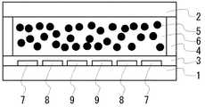
図1に本発明の代表的な断面構成図を、図7に本発明の代表的な平面図を示す。第一基板1上には第1電極7と第3電極9が配置されており、絶縁部3を挟んで第2電極8と第4電極10が配置されている。この場合、第1、第2、第3及び第4電極の4電極によって1つの電極群が構成されており、図7に示すように2つの電極群が存在し、各電極が周期的に配列している。さらにその上に間隙支持体4を挟んで第二基板2が配置されている。
【0010】
第一基板1と第二基板2と間隙支持体4によって作られる空間には透明な絶縁性液体6が充填され、その絶縁性液体6中に電界印加によって泳動する不透明帯電泳動粒子5が分散されている。第1電極7、第2電極8、第3電極9、第4電極10の平面パターンは環状であり、それを同心円状に配置している。図中にそれぞれ4本ずつ配置された第1電極7、第2電極8、第3電極9、第4電極10は、それぞれの電極同士が外部で結線され、電気的に接続されている。
【0011】
第一基板、第二基板は、実質的に光学的に透明である。なお、本発明において、実質的に透明であるとは、光透過率が可視光域(波長400−700nm)或は変調しようとする波長領域において、70%以上、好ましくは80%以上、より好ましくは90%以上であることを意味する。
【0012】
透明な電極のうち1つの電極群を形成する電極数は、3つ以上ならいくらでも良い。また上記電極群が1つであり、その中の電極数が3の場合を図2に示す。さらにこの電極数は、3電極以上あれば良く、かつ電極群数が複数あり、その電極パターンが周期的に配置されている場合が好ましい。この場合電極上に浮遊する不透明帯電泳動粒子を、一方の電極から他方の電極へ搬送することが可能であり、電極数が3を下回ると動作が不完全となる。
【0013】
ここで云う周期的とはこの電極群数をNとすると、第1電極7の平面方向の隣に第2電極8を配置し、その第2電極8の平面方向の隣に第3電極9を配置し、・・・、順次に第n電極の平面方向の隣に再度第1電極7を配置する構成を指す。ただし、電極群数が1つの場合は、第1電極7の平面方向の隣に第2電極8を配置し、その第2電極8の平面方向の隣に第3電極9を配置する構成に従って第n電極までを配置すればよい。また、各電極群に含まれる電極数はすべて等しくなくても良い。nを2以上の整数とすると、1電極群の最後の第n電極の隣に、次の電極群に属する第1電極が配置されていれば良い。
【0014】
電極は一方の基板のみに配置しても良いが両方の基板に配置しても良い。すくなくとも各電極は基板の対向面側に配置し平面方向にずらした位置に配置すればよい。電極は全面を覆うようにに配置するのが好ましいが(図1、図4)、その限りではない。全面を覆ってもいいし覆わなくても良い。つまり電極間に隙間があってよい(図2、図5)。さらには電極同士が一部重複していて配置されても良い(図3)。電極に透明電極を用いるのは好ましい構成だが、電極が全面を覆わない場合は透明電極でなくても良い。電極が全面を覆う場合には少なくとも一部の電極が透明であれば良い。
【0015】
不透明帯電泳動粒子5は電極に印加された電圧により発生する電場に依存して泳動する。例えば不透明帯電泳動粒子5が正に帯電している場合、不透明帯電泳動粒子5は最も低い電圧が印加された電極近傍に集まる。最も低い電圧を印加する電極を第1電極7、第2電極8・・・と替えると不透明帯電泳動粒子5は第1電極7に集まった後、第2電極8に集まる。これを繰り返すことで不透明帯電泳同粒子5を電気泳動光量調整素子21内で移動可能となり、不透明帯電泳同粒子5を凝集分散させ電気泳動光量調整素子21の透過光量を調整できる。また、不透明帯電泳動粒子5を逆方向へ移動させる場合には図12に示すように印加電圧の位相を逆にすればよい。
【0016】
駆動電圧の波形は特に限定しない。矩形波(図10)、正弦波、三角波などどのようの駆動波形でも良い。各電極に印加する駆動波形の位相差も特に限定しないが、均等な位相差をもって入力するのが好ましい(図11)。例えば電極群数がn個の場合、各電極間の位相差は2π/nとなる。
【0017】
不透明帯電泳動粒子5の駆動方法として、実効的な電界強度を徐々に増減させることは良い駆動方法の一つである(図13)。各電極に印加する電圧の入力波形は正弦波、矩形波などを位相をずらして入力すればよいが、それよりも低い周波数で電圧を増減させて入力しても良い。本素子は第1電極7から第2電極8、第2電極8から第3電極9、第3電極9から・・・と不透明帯電泳動粒子5を移動させて駆動するが、その第1電極7から第2電極8へ移動させる電圧と第2電極8から第3電極9へ移動させる電圧を僅かに変えることで粒子の搬送量を変化させ、粒子を均一に分散可能となる。例えば電圧を以下の式で与えられる値にして入力する駆動方法は1つの例である。
【0018】
【外1】
(但しf:周波数、t:時間、n:電極群の番号、N:電極群数、α:−1以上1以下の実数)
または図13に示すように駆動電圧の高さを徐々に低下もしくは増加させるサイクルを繰り返しても良い。
【0020】
電気泳動調光素子21の一部に不透明帯電泳動粒子5を集合させて透光状態をなし(図1),電気泳動調光素子21全体に不透明帯電泳動粒子5を分散させて半透光状態を成す(図2)のは良い駆動方法の1つである。透光状態をなす際に不透明帯電泳動粒子5を集合させる場所は素子内であればどこでも良い。素子中央に集めても良いし、素子周辺部に集めても良い(図1)。または1つ以上の電極群上に集めても良い。
【0021】
電気泳動調光素子21の一部に不透明な遮光部11を備える構成は好ましい構成の1つである(図4、図5、図8、図9)。遮光部11の構成は特に限定しない。一部が透明で一部が不透明な基板(図3)もしくは不透明な基板に穴をあけたもの(図4、図5)を第一基板1もしくは第二基板2の上に設けてもよいし、第一基板1もしくは第二基板2を不透明に着色しても良い。または一部が不透明な基板を第一基板1もしくは第二基板2に用いても良い。または、不透明の電極材料で電極を作成し遮光部11としても良い。
【0022】
遮光領域も特に限定しない。素子中央でもよいし、周辺部分(図8、図9)でも良い。一部を不透明材料で作成した電極を遮光部分としても良い。
【0023】
遮光部1に不透明帯電泳動粒子5を搬送して透光状態をなし、開口部12の一部もしくは全部に粒子を搬送して、半透光状態を成す方法は好ましい駆動方法の1つである。遮光部11に不透明帯電泳動粒子5を集めることで透光状態の透過率が一定になる。また不透明帯電泳動粒子5を開口部12の全部に分散して半透光状態をなしてもよいし(図8)、開口部12の一部に移動させて一部透光部分を残して半透光状態にする(図9)のも良い駆動方法である。不透明な電極と一部の透明な電極上に粒子を移動させて半透光状態をなすのも良い駆動方法である。
【0024】
絶縁部3を介して配置される電極層を2電極層以上備え、2つ以上でかつ全電極群数の半数以下の電極群を1つの電極層に配置することは好ましい構成の1つである。図2に示すように、電極間には絶縁部3もしくは電極間に隙間を作るなど、少なくとも絶縁を保つ部分が必要である。電極を全面に配置する場合、電極層を2つ以上備えかつ全電極群数の半数以下の電極群を1つの電極層に配置することで電極間の隙間の無い構成が可能となる(図1)。また、1つの電極層に2つ以上の電極群を配置することで電極層数を減少でき、製造が容易となる。好ましい構成としては2電極群を備えた電極層を第一基板1および第二基板2に1電極層ずつ(図3)もしくは2電極層ずつ(図4)を備える構成である。
【0025】
図7は、電極の形状が径の異なる環状で、それぞれの電極を同心に配置する構成は好ましい構成の1つである。電極の太さは特に限定しない。全ての電極で同じでもよいし、例えば電極の径に依存して変化しても良い。また、電極は完全な環でなくても良く、配線をするために環の一部を切断して配線を配置しても良い。環状の電極の最内部に配置される電極は必ずしも環状でなくても良く、例えば円の様に、その電極の内部を電極領域として含んでも良い。
【0026】
図6は、帯状の電極を配置し、その一部もしくは全部を素子の遠心方向に対して0度でない角度を持って配置する構成は好ましい構成の一つである。電極が遠心方向に対して0度でない角度で配置されることで不透明帯電泳動粒子5を遠心方向と円周方向に同時に搬送することができ、素子内の不透明帯電泳動粒子5の分布濃度を均一化できる。電極と遠心方向の成す角度は特に限定しない。一定でもよいし、素子中心からの距離に依存して変化しても良い。また電極の幅も特に限定しない。一定でもよいし、図6のように素子中心からの距離に依存して変化しても良い。
【0027】
不透明帯電泳動粒子5を所望の領域に移動させた後に、異なる2つの電圧をそれぞれ1つ以上の電極群に印加し、かつ電圧を交互に入れ替える方法は良い駆動方法の一つである。さらに、不透明帯電泳動粒子5にかかる実効的な電界強度を徐々に低下させて、電極の印加電圧を同じにする駆動方法も好ましい駆動方法である。これらの駆動方法により不透明帯電泳動粒子の分布が均一になり、透過率制御が容易となる。
【0028】
本素子を用いた好ましい撮像素子の例を図14に示す。各電極群に所望の電圧を印加する駆動回路23と素子を通過する光量を測定する光量測定手段22を備えている。光量測定手段22はどのようなものでも良い。例えば電荷結合素子などの撮像素子36を光量測定手段22に用いて、その出力に依存して適切な透過率になるように駆動回路23により電気泳動光量調整素子21を制御すればよい。
【0029】
またこの電気泳動光量調整素子35の適用方法は特に限定しないが、レンズ装置33、撮像モジュール32、および撮像装置31などに適用するのは良い適用方法である。一例を図15に示す。
【0030】
また本発明の電気泳動光量調整素子は、レンズと撮像素子などの光学部品の光軸上に配置すればその配置方法について特に限定しない。この一例を図16に示すが、本発明の電気泳動光量調整素子165をレンズ装置164の絞り位置に対応した場所に配置した例(図16−a)、もしくはレンズ164の前面に配置する構成(図16−b)は好ましい構成例である。
【0031】
レンズ装置を構成するレンズの枚数は特に限定しない。複数枚で構成しても良いし、1枚でもよい。少なくとも撮像素子に入射する光量を変化させることが出来て、かつ結像面で所望の像が得られればよく、どの位置に配置してもよい。これによってよって結像面に撮像素子166を配置することによって、入射光の光量を調節することが可能になる。
【0032】
【実施例】
以下、実施例に従って本発明を説明する。
【0033】
(実施例1)
本実施例では、図1に示す断面構成で、図7に示す平面構成の素子を作製し駆動を行った。
【0034】
作製した素子の大きさは直径1mm、厚さ0.53mmである。まず、第一基板1として厚さ0.2mmのガラスにITOを低温成膜し、フォトリソグラフィー及びエッチングにより図に示す形状にパターニングした。続いて、絶縁部としてSiO2を製膜し、その上にITOを低温成膜し、フォトリソグラフィー及びエッチングにより図に示す形状にパターニングした。また、同様に絶縁部としてSiO2を製膜した。この上に、間隙支持体4を形成した。間隙支持体4は、光感光性エポキシ樹脂を塗布した後、露光及びウエット現像を行うことによって形成し、30μmの高さとした。形成された空間内に絶縁性液体6及び不透明帯電泳動粒子5を充填した。絶縁性液体6としては、イソパラフィンを使用した。不透明帯電泳動粒子5としては、ポリスチレンとカーボンの混合物で、平均粒径2μm位のものを使用した。イソパラフィン中での不透明帯電泳動粒子5は正帯電極性を示した。次に、第2基板2として厚さ0.2mmのガラスを位置合わせを行ないながら第一基板1上に置き、素子周辺部を接着剤により張り合わせた。
【0035】
これに駆動装置23を接続して駆動を行った。まず、図11に示す波形により素子を駆動させたところ、素子全体に分散していた不透明帯電泳動粒子5は素子中央に搬送され透光状態となった。駆動電圧は10Vである。また、図12に示す波形により素子を駆動させたところ、素子中央に分散していた不透明帯電泳動粒子5は素子周辺に搬送され透光状態となった。駆動電圧は同様に10Vである。
【0036】
また、図13に示す波形により素子を駆動させたところ、素子周辺に分散していた不透明帯電泳動粒子5は素子全体に分散され半透光光状態となった。駆動電圧は最高10Vである。また第1電極7と第3電極9、第2電極8と第4電極10をそれぞれ同電位として、一方に5V他方に−5Vを交互に印加したところ不透明帯電泳動粒子5は均一に分散した。さらに、電圧を緩やかに小さくして全ての電極を0Vにしたところより均一に分散した。
【0037】
この駆動装置に光量測定手段22を接続し、その光量測定手段22の出力に依存して上記駆動電圧を選択して印加したところ、電気泳動光量調整素子21を透過する光量を一定に保つことができた。また、本素子を撮像装置31に取り付けて駆動させたところ、明所から暗所まで良好な画像を得ることができた。
【0038】
(実施例2)
本実施例では、図5に示す断面構成で、図6に示す平面構成の素子を作製し駆動を行った。
【0039】
作製した素子の大きさは直径1mm、厚さ0.53mmである。まず、第一基板1として厚さ0.2mmのガラスにITOを低温成膜し、フォトリソグラフィー及びエッチングにより図に示す形状にパターニングした。続いて、絶縁部としてSiO2を製膜した。この上に、間隙支持体4を形成した。間隙支持体4は、光感光性エポキシ樹脂を塗布した後、露光及びウエット現像を行うことによって形成し、30μmの高さとした。形成された空間内に絶縁性液体6及び不透明帯電泳動粒子5を充填した。絶縁性液体6としては、イソパラフィンを使用した。不透明帯電泳動粒子5としては、ポリスチレンとカーボンの混合物で、平均粒径2μm位のものを使用した。イソパラフィン中での不透明帯電泳動粒子5は正帯電極性を示した。次に、第2基板2として厚さ0.2mmのガラスを位置合わせを行ないながら第一基板1上に置き、素子周辺部を接着剤により張り合わせた。その上に直径0.7mmの穴をあけた不透明な基板を配置して遮光部とした。
【0040】
これに駆動装置23を接続して駆動を行った。まず、図12に示す波形により素子を駆動させたところ、素子全体に分散していた不透明帯電泳動粒子5は素子周辺に搬送され透光状態となった。駆動電圧は10Vである。また、図13に示す波形により素子を駆動させたところ、素子周辺に分散していた不透明帯電泳動粒子5は素子全体に分散され半透光光状態となった(図8)。駆動電圧は最高10Vである。また、図11に示す波形により素子を駆動させたところ、素子全体に分散していた不透明帯電泳動粒子5は素子中央に搬送され半透光状態となった(図9)。駆動電圧は同様に10Vである。また第1電極7と第3電極9、第2電極8と第4電極10をそれぞれ同電位として、一方に5V他方に−5Vを交互に印加したところ不透明帯電泳動粒子5は均一に分散した。さらに、電圧を緩やかに小さくして全ての電極を0Vにしたところより均一に分散した。
【0041】
この駆動装置に光量測定手段22を接続し、その光量測定手段22の出力に依存して上記駆動電圧を選択して印加したところ、電気泳動光量調整素子21を透過する光量を一定に保つことができた。また、本素子を撮像モジュール32に取り付けて駆動させたところ、明所から暗所まで良好な画像を得ることができた。
【0042】
【発明の効果】
以上、詳細に述べたように、本発明によって次のような効果が得られた。
第一に、1つの素子で透過率が変化する電気泳動光量調整素子を提供した。これによりこれまで小型化が困難であったレンズ装置、撮像モジュール、撮像装置を大幅に小型化できた。
【0043】
第二に、無段階で透過率を変化できることから動画の撮影中にも透過率を変えることができ、より良好な動画像の撮影が可能となった。
【図面の簡単な説明】
【図1】本発明の電気泳動光量調整素子の代表的な断面図の一例を示す。
【図2】本発明の電気泳動光量調整素子の代表的な断面図の一例を示す。
【図3】本発明の電気泳動光量調整素子の代表的な断面図の一例を示す。
【図4】本発明の電気泳動光量調整素子の代表的な断面図の一例を示す。
【図5】本発明の電気泳動光量調整素子の代表的な断面図の一例を示す。
【図6】本発明の電気泳動光量調整素子の代表的な平面図の一例を示す。
【図7】本発明の電気泳動光量調整素子の代表的な平面図の一例を示す。
【図8】本発明の電気泳動光量調整素子の代表的な平面図の一例を示す。
【図9】本発明の電気泳動光量調整素子の代表的な平面図の一例を示す。
【図10】本発明の電気泳動光量調整素子の代表的な駆動方法の一例を示す。
【図11】本発明の電気泳動光量調整素子の代表的な駆動方法の一例を示す。
【図12】本発明の電気泳動光量調整素子の代表的な駆動方法の一例を示す。
【図13】本発明の電気泳動光量調整素子の代表的な駆動方法の一例を示す。
【図14】本発明の電気泳動光量調整素子の代表的な適用方法の一例を示す。
【図15】本発明の電気泳動光量調整素子の代表的な適用方法の一例を示す。
【図16】本発明の電気泳動光量調整素子を用いた撮像装置の一例を示す図である。
【符号の説明】
1 第一基板
2 第二基板
3 絶縁部
4 間隙支持体
5 不透明帯電泳動粒子
6 絶縁性液体
7 第1電極
8 第2電極
9 第3電極
10 第4電極
11 遮光部
12 開口部
21 電気泳動光量調整素子
22 光量測定手段
23 駆動装置
31 撮像装置
32 撮像モジュール
33 レンズ装置
34 レンズ
35 電気泳動光量調整素子
36 撮像素子
37 撮像素子駆動装置
38 駆動装置
39 記憶装置[0001]
BACKGROUND OF THE INVENTION
The present invention relates to a light amount adjusting element which is provided on an optical axis of a lens and whose transmittance changes according to the light amount, a driving method thereof, a driving device, and a device using the same.
[0002]
[Prior art]
Japanese Laid-Open Patent Publication No. 05-040293 discloses a video / camera interchangeable lens light amount adjusting device that automatically adjusts the light amount by selectively inserting and removing filters having different transmittances on and off the optical axis. In this invention, a filter holder holding a plurality of filters having different transmittances is provided in a lens barrel, and an appropriate amount of light is obtained by driving the filter holder according to information from a camera body in which the lens barrel is assembled. A drive source for selectively exchanging the filter on the optical axis, and when the camera body is turned on and enters a shooting standby state, the filter body is driven to adjust the light amount, and the camera body is in a recording state. In this case, the light amount adjusting device is configured to restrict the light amount adjusting operation.
[0003]
[Problems to be solved by the invention]
However, the light amount adjusting device disclosed in Japanese Patent Laid-Open No. 05-040293 is difficult to reduce in size because it holds a plurality of filters and actuators. -Since the transmittance by the filter changes discontinuously, it is difficult to switch during shooting of a moving image or the like. Or, there is a concern that an unnatural image may be generated when switching.
There are problems such as.
[0004]
[Means for Solving the Problems]
The inventor has analyzed the problems as described above and found that the above problems can be improved by providing one element capable of changing the amount of transmitted light in a stepless manner. Accordingly, an object of the present invention is to provide an electrophoretic light amount adjusting element that improves the above-mentioned problems of the prior art and changes the transmitted light amount state by moving the opaque charged electrophoretic particles by an electric signal.
[0005]
A first aspect of the present invention is a light amount adjusting element that adjusts a transmitted light amount, and is a substantially transparent first substrate and a substantially transparent substrate disposed to face the first substrate through a gap support. A second substrate, an electrophoretic liquid composed of a transparent insulating liquid and a plurality of opaque charged electrophoretic particles filled between the two substrates, and at least one opposing surface side of the two substrates being sequentially shifted in the plane direction.A plurality of electrode groups including three or more electrodes arranged,
The electrodes in each electrode group are electrically connected to the corresponding electrodes in the other electrode groups,
The light amount adjusting element is characterized in that a driving voltage for collecting the opaque charged electrophoretic particles to one of the three or more electrodes is sequentially applied to the three or more electrodes while being shifted in time in the order of the arrangement.
[0007]
Further,the light amount adjusting device, thefirst substrate or the second substrateand a non-translucent regions and the light-transmitting region, said to set an opaque electrophoretic particles in the non-light-transmissive regiontransmitting state and thesaid opaque electrophoretic particlestransmitted light amount anda translucent state or non-transmissive state isdispersed in a part or all of the light transmitting regionis adjusted preferably.
[0008]
DETAILED DESCRIPTION OF THE INVENTION
Hereinafter, embodiments of the present invention will be described in order.
[0009]
FIG. 1 shows a typical sectional configuration diagram of the present invention, and FIG. 7 shows a typical plan view of the present invention. A
[0010]
A space formed by the
[0011]
The first substrate and the second substrate are substantially optically transparent. In the present invention, substantially transparent means that the light transmittance is 70% or more, preferably 80% or more, more preferably in the visible light region (wavelength 400 to 700 nm) or the wavelength region to be modulated. Means 90% or more.
[0012]
Of the transparent electrodes, the number of electrodes forming one electrode group may be any number as long as it is three or more. FIG. 2 shows the case where there is one electrode group and the number of electrodes in the electrode group is three. Further, the number of electrodes may be three or more, and there are a plurality of electrode groups, and the electrode patterns are preferably arranged periodically. In this case, the opaque charged electrophoretic particles floating on the electrode can be transported from one electrode to the other electrode, and when the number of electrodes is less than 3, the operation becomes incomplete.
[0013]
Here, the term “periodic” means that the number of electrode groups is N, the
[0014]
The electrodes may be disposed on only one substrate, but may be disposed on both substrates. At least each electrode may be arranged on the opposite surface side of the substrate and at a position shifted in the plane direction. The electrodes are preferably arranged so as to cover the entire surface (FIGS. 1 and 4), but this is not a limitation. The entire surface may or may not be covered. That is, there may be a gap between the electrodes (FIGS. 2 and 5). Furthermore, the electrodes may be partially overlapped and arranged (FIG. 3). Although it is preferable to use a transparent electrode for the electrode, it may not be a transparent electrode if the electrode does not cover the entire surface. When the electrode covers the entire surface, at least a part of the electrode may be transparent.
[0015]
The opaque charged
[0016]
The waveform of the drive voltage is not particularly limited. Any driving waveform such as a rectangular wave (FIG. 10), a sine wave, or a triangular wave may be used. The phase difference of the drive waveform applied to each electrode is not particularly limited, but it is preferable to input with a uniform phase difference (FIG. 11). For example, when the number of electrode groups is n, the phase difference between the electrodes is 2π / n.
[0017]
As a method for driving the opaque charged
[0018]
[Outside 1]
(Where f: frequency, t: time, n: number of electrode groups, N: number of electrode groups, α: real number from −1 to 1)
Alternatively, as shown in FIG. 13, a cycle for gradually decreasing or increasing the drive voltage may be repeated.
[0020]
The opaque charged
[0021]
A configuration in which the opaque
[0022]
The light shielding area is not particularly limited. The center of the element or the peripheral portion (FIGS. 8 and 9) may be used. An electrode partially made of an opaque material may be used as the light shielding portion.
[0023]
One preferred driving method is a method in which the opaque charged
[0024]
It is one of the preferable configurations that two or more electrode layers are provided via the insulating
[0025]
In FIG. 7, a configuration in which the electrodes are in an annular shape with different diameters and the electrodes are arranged concentrically is one of the preferable configurations. The thickness of the electrode is not particularly limited. It may be the same for all electrodes, or may vary depending on, for example, the diameter of the electrodes. In addition, the electrode may not be a complete ring, and in order to perform wiring, a part of the ring may be cut and the wiring may be arranged. The electrode arranged at the innermost part of the annular electrode does not necessarily have to be annular, and for example, the inside of the electrode may be included as an electrode region like a circle.
[0026]
FIG. 6 shows a preferred configuration in which strip-like electrodes are arranged and a part or all of them are arranged at an angle other than 0 degrees with respect to the centrifugal direction of the element. By arranging the electrodes at an angle other than 0 degrees with respect to the centrifugal direction, the opaque charged
[0027]
A method of moving the opaque charged
[0028]
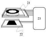
An example of a preferable image sensor using this element is shown in FIG. A
[0029]
The application method of the electrophoretic light
[0030]
The electrophoretic light amount adjusting element of the present invention is not particularly limited as to the arrangement method as long as it is arranged on the optical axis of an optical component such as a lens and an imaging element. An example of this is shown in FIG. 16, and an example in which the electrophoretic light
[0031]
The number of lenses constituting the lens device is not particularly limited. It may be composed of a plurality of sheets or a single sheet. As long as at least the amount of light incident on the image sensor can be changed and a desired image can be obtained on the imaging plane, it may be arranged at any position. Accordingly, it is possible to adjust the amount of incident light by disposing the
[0032]
【Example】
Hereinafter, the present invention will be described according to examples.
[0033]
(Example 1)
In this example, an element having the cross-sectional configuration shown in FIG. 1 and the planar configuration shown in FIG. 7 was produced and driven.
[0034]
The size of the manufactured element is 1 mm in diameter and 0.53 mm in thickness. First, an ITO film was formed at a low temperature on a glass having a thickness of 0.2 mm as the
[0035]
The
[0036]
Further, when the device was driven by the waveform shown in FIG. 13, the opaque charged
[0037]
When the light quantity measuring means 22 is connected to this driving device, and the drive voltage is selected and applied depending on the output of the light quantity measuring means 22, the light quantity transmitted through the electrophoretic light
[0038]
(Example 2)
In this example, an element having the cross-sectional configuration shown in FIG. 5 and the planar configuration shown in FIG. 6 was produced and driven.
[0039]
The size of the manufactured element is 1 mm in diameter and 0.53 mm in thickness. First, an ITO film was formed at a low temperature on a glass having a thickness of 0.2 mm as the
[0040]
The
[0041]
When the light quantity measuring means 22 is connected to this driving device, and the drive voltage is selected and applied depending on the output of the light quantity measuring means 22, the light quantity transmitted through the electrophoretic light
[0042]
【The invention's effect】
As described above in detail, the present invention has the following effects.
First, an electrophoretic light amount adjusting element in which the transmittance is changed by one element is provided. As a result, the lens device, the imaging module, and the imaging device that have been difficult to miniaturize can be greatly reduced in size.
[0043]
Secondly, since the transmittance can be changed in a stepless manner, the transmittance can be changed even during shooting of a moving image, and a better moving image can be shot.
[Brief description of the drawings]
FIG. 1 shows an example of a typical sectional view of an electrophoretic light amount adjusting element of the present invention.
FIG. 2 shows an example of a typical sectional view of an electrophoretic light amount adjusting element of the present invention.
FIG. 3 shows an example of a typical sectional view of an electrophoretic light amount adjusting element of the present invention.
FIG. 4 shows an example of a typical sectional view of an electrophoretic light amount adjusting element of the present invention.
FIG. 5 shows an example of a typical sectional view of an electrophoretic light amount adjusting element of the present invention.
FIG. 6 shows an example of a typical plan view of an electrophoretic light amount adjusting element of the present invention.
FIG. 7 shows an example of a typical plan view of an electrophoretic light amount adjusting element of the present invention.
FIG. 8 shows an example of a typical plan view of an electrophoretic light amount adjusting element of the present invention.
FIG. 9 shows an example of a typical plan view of an electrophoretic light amount adjusting element of the present invention.
FIG. 10 shows an example of a typical driving method of the electrophoretic light amount adjusting element of the present invention.
FIG. 11 shows an example of a typical driving method of the electrophoretic light amount adjusting element of the present invention.
FIG. 12 shows an example of a typical driving method of the electrophoretic light amount adjusting element of the present invention.
FIG. 13 shows an example of a typical driving method of the electrophoretic light amount adjusting element of the present invention.
FIG. 14 shows an example of a typical application method of the electrophoretic light amount adjusting element of the present invention.
FIG. 15 shows an example of a typical application method of the electrophoretic light amount adjusting element of the present invention.
FIG. 16 is a diagram illustrating an example of an imaging apparatus using the electrophoretic light amount adjusting element of the present invention.
[Explanation of symbols]
DESCRIPTION OF
Claims (7)
Translated fromJapanese実質的に透明な第一基板と、該第一基板に間隙支持体を介して対向して配置された実質的に透明な第二基板と、前記両基板間に充填された透明絶縁性液体と複数の不透明帯電泳動粒子からなる電気泳動液と、前記両基板の少なくとも一方の対向面側の、平面方向に順次ずれて配置された3以上の電極を含む複数の電極群とを有し、
各電極群中の電極が他の電極群中の相対応する電極と電気的に結線されており、
前記不透明帯電泳動粒子を前記3以上の電極の1つに集める駆動電圧が、前記配置の順に時間的にずれて前記3以上の電極に順次印加されることを特徴とする光量調整素子。A light amount adjusting element for adjusting a transmitted light amount,
A substantially transparent first substrate, a substantially transparent second substrate disposed opposite to the first substrate via a gap support, and a transparent insulating liquid filled between the substrates. An electrophoretic liquid composed of a plurality of opaque charged electrophoretic particles,and a plurality of electrode groups including three or more electrodes arranged sequentially shifted in a plane direction on at least one opposing surface side of the both substrates,
The electrodes in each electrode group are electrically connected to the corresponding electrodes in the other electrode groups,
A light amount adjusting element, wherein a driving voltage for collecting the opaque charged electrophoretic particles to one of the three or more electrodes is sequentially applied to the three or more electrodes in a time-shifted order.
Priority Applications (1)
| Application Number | Priority Date | Filing Date | Title |
|---|---|---|---|
| JP2002219705AJP4164308B2 (en) | 2002-07-29 | 2002-07-29 | Light amount adjusting element and imaging apparatus using the same |
Applications Claiming Priority (1)
| Application Number | Priority Date | Filing Date | Title |
|---|---|---|---|
| JP2002219705AJP4164308B2 (en) | 2002-07-29 | 2002-07-29 | Light amount adjusting element and imaging apparatus using the same |
Publications (2)
| Publication Number | Publication Date |
|---|---|
| JP2004061834A JP2004061834A (en) | 2004-02-26 |
| JP4164308B2true JP4164308B2 (en) | 2008-10-15 |
Family
ID=31940541
Family Applications (1)
| Application Number | Title | Priority Date | Filing Date |
|---|---|---|---|
| JP2002219705AExpired - Fee RelatedJP4164308B2 (en) | 2002-07-29 | 2002-07-29 | Light amount adjusting element and imaging apparatus using the same |
Country Status (1)
| Country | Link |
|---|---|
| JP (1) | JP4164308B2 (en) |
Cited By (2)
| Publication number | Priority date | Publication date | Assignee | Title |
|---|---|---|---|---|
| WO2015131512A1 (en)* | 2014-03-06 | 2015-09-11 | 京东方科技集团股份有限公司 | 3d conversion lens, 3d glasses, and control method therefor |
| KR20230013917A (en)* | 2021-07-20 | 2023-01-27 | 주식회사 그린에코스 | A smart aquaponics dome system |
Families Citing this family (9)
| Publication number | Priority date | Publication date | Assignee | Title |
|---|---|---|---|---|
| JP4557891B2 (en) | 2006-01-06 | 2010-10-06 | キヤノン株式会社 | Driving method of electrophoretic display device |
| EP1830345A1 (en)* | 2006-03-02 | 2007-09-05 | THOMSON Licensing | Driving scheme of a variable electrophoretic optical iris diaphragm |
| CN102385210B (en)* | 2010-08-30 | 2016-03-02 | 鸿富锦精密工业(深圳)有限公司 | Aperture and adopt the camera module of this aperture |
| KR101882734B1 (en)* | 2011-08-22 | 2018-08-27 | 삼성디스플레이 주식회사 | Electrophoretic display device |
| KR101973339B1 (en)* | 2018-11-21 | 2019-04-26 | 김광수 | Electronic Aperture |
| JP7145738B2 (en)* | 2018-11-28 | 2022-10-03 | Tianma Japan株式会社 | Beam direction controller |
| KR102142245B1 (en)* | 2019-04-22 | 2020-08-06 | 김광수 | Electronic Aperture |
| CN111240121B (en)* | 2020-02-21 | 2024-05-28 | 京东方科技集团股份有限公司 | Transparent control device and display screen |
| CN116943044B (en)* | 2023-09-18 | 2023-11-24 | 东莞市红富照明科技有限公司 | Far infrared physiotherapy lamp based on electrophoresis control |
- 2002
- 2002-07-29JPJP2002219705Apatent/JP4164308B2/ennot_activeExpired - Fee Related
Cited By (4)
| Publication number | Priority date | Publication date | Assignee | Title |
|---|---|---|---|---|
| WO2015131512A1 (en)* | 2014-03-06 | 2015-09-11 | 京东方科技集团股份有限公司 | 3d conversion lens, 3d glasses, and control method therefor |
| US10241343B2 (en) | 2014-03-06 | 2019-03-26 | Boe Technology Group Co., Ltd. | 3D conversion lens, 3D glasses and control method thereof |
| KR20230013917A (en)* | 2021-07-20 | 2023-01-27 | 주식회사 그린에코스 | A smart aquaponics dome system |
| KR102698011B1 (en)* | 2021-07-20 | 2024-08-22 | 주식회사 그린에코스 | A smart aquaponics dome system |
Also Published As
| Publication number | Publication date |
|---|---|
| JP2004061834A (en) | 2004-02-26 |
Similar Documents
| Publication | Publication Date | Title |
|---|---|---|
| JP4164308B2 (en) | Light amount adjusting element and imaging apparatus using the same | |
| US5745281A (en) | Electrostatically-driven light modulator and display | |
| US8061910B2 (en) | Micro shutter having iris function, method for manufacturing the same, and micro camera module having the same | |
| CN107219573B (en) | Fresnel lenses and glasses | |
| KR101410708B1 (en) | Reflective display panel and method for manufacturing such a display panel | |
| TW201300911A (en) | Three-dimensional image capturing device | |
| JP4684448B2 (en) | LIGHT MODULATION DEVICE, ITS MODULATION DEVICE MANUFACTURING METHOD, IMAGE FORMING DEVICE HAVING THE LIGHT MODULATION DEVICE, AND IMAGE PROJECTION DISPLAY DEVICE HAVING THE LIGHT MODULATION DEVICE | |
| CN103066069A (en) | TFT array substrate, electronic paper display panel and forming method thereof | |
| CN112379560A (en) | Diaphragm and diaphragm module | |
| US3973957A (en) | Imaging method including exposure of deformation imaging member through lenticular lens element | |
| JP2004061831A (en) | Electrophoretic light intensity adjustment element | |
| JP2004061833A (en) | Electrophoretic light quantity adjusting element, driving method thereof and apparatus using the same | |
| KR101534626B1 (en) | Electrophoretic display device and method of forming the partition wall | |
| CN115047687B (en) | Array device capable of independently controlling lens units, imaging device and driving method | |
| JP4033148B2 (en) | Lens barrel and imaging device | |
| JP4989949B2 (en) | Liquid crystal optical element and liquid crystal optical module | |
| JP2004061839A (en) | Electrophoretic light quantity adjusting element and its driving method | |
| JP3714083B2 (en) | Focal position variable spatial modulation device | |
| CN219831490U (en) | optical lens | |
| JP2004061832A (en) | Light amount adjusting element, driving method thereof and apparatus using the same | |
| US3997243A (en) | Color image reproduction system | |
| JP2007047363A (en) | Electrophoretic light amount adjusting element, driving method thereof, and imaging apparatus using the same | |
| JPH0211349A (en) | Liquid crystal shutter array apparatus and optical scanning apparatus using the same | |
| KR20170119149A (en) | Apparatus for electrically adjusting quantity of light, camera module including the apparatus, and the mobile device including the module | |
| JPH0283559A (en) | optical printer |
Legal Events
| Date | Code | Title | Description |
|---|---|---|---|
| A621 | Written request for application examination | Free format text:JAPANESE INTERMEDIATE CODE: A621 Effective date:20050714 | |
| A131 | Notification of reasons for refusal | Free format text:JAPANESE INTERMEDIATE CODE: A131 Effective date:20070123 | |
| A521 | Written amendment | Free format text:JAPANESE INTERMEDIATE CODE: A523 Effective date:20070326 | |
| A131 | Notification of reasons for refusal | Free format text:JAPANESE INTERMEDIATE CODE: A131 Effective date:20080415 | |
| A521 | Written amendment | Free format text:JAPANESE INTERMEDIATE CODE: A523 Effective date:20080616 | |
| TRDD | Decision of grant or rejection written | ||
| A01 | Written decision to grant a patent or to grant a registration (utility model) | Free format text:JAPANESE INTERMEDIATE CODE: A01 Effective date:20080708 | |
| A01 | Written decision to grant a patent or to grant a registration (utility model) | Free format text:JAPANESE INTERMEDIATE CODE: A01 | |
| A61 | First payment of annual fees (during grant procedure) | Free format text:JAPANESE INTERMEDIATE CODE: A61 Effective date:20080728 | |
| FPAY | Renewal fee payment (event date is renewal date of database) | Free format text:PAYMENT UNTIL: 20110801 Year of fee payment:3 | |
| R150 | Certificate of patent or registration of utility model | Free format text:JAPANESE INTERMEDIATE CODE: R150 | |
| FPAY | Renewal fee payment (event date is renewal date of database) | Free format text:PAYMENT UNTIL: 20120801 Year of fee payment:4 | |
| FPAY | Renewal fee payment (event date is renewal date of database) | Free format text:PAYMENT UNTIL: 20120801 Year of fee payment:4 | |
| FPAY | Renewal fee payment (event date is renewal date of database) | Free format text:PAYMENT UNTIL: 20130801 Year of fee payment:5 | |
| LAPS | Cancellation because of no payment of annual fees |