JP4161262B2 - ORGANIC ELECTROLUMINESCENT ELEMENT AND LIGHT EMITTING OR DISPLAY DEVICE USING THE SAME - Google Patents
ORGANIC ELECTROLUMINESCENT ELEMENT AND LIGHT EMITTING OR DISPLAY DEVICE USING THE SAMEDownload PDFInfo
- Publication number
- JP4161262B2 JP4161262B2JP2003165852AJP2003165852AJP4161262B2JP 4161262 B2JP4161262 B2JP 4161262B2JP 2003165852 AJP2003165852 AJP 2003165852AJP 2003165852 AJP2003165852 AJP 2003165852AJP 4161262 B2JP4161262 B2JP 4161262B2
- Authority
- JP
- Japan
- Prior art keywords
- organic electroluminescent
- layer
- structural formula
- light
- electroluminescent element
- Prior art date
- Legal status (The legal status is an assumption and is not a legal conclusion. Google has not performed a legal analysis and makes no representation as to the accuracy of the status listed.)
- Expired - Fee Related
Links
- 239000010410layerSubstances0.000claimsdescription549
- -1styryl compoundChemical group0.000claimsdescription123
- 239000000463materialSubstances0.000claimsdescription72
- 230000005525hole transportEffects0.000claimsdescription65
- 239000012044organic layerSubstances0.000claimsdescription32
- 238000005401electroluminescenceMethods0.000claimsdescription24
- 239000000470constituentSubstances0.000claimsdescription3
- 238000005259measurementMethods0.000description197
- 239000012299nitrogen atmosphereSubstances0.000description189
- 239000010408filmSubstances0.000description141
- 238000001228spectrumMethods0.000description102
- 238000000034methodMethods0.000description99
- 230000015572biosynthetic processEffects0.000description98
- 230000015556catabolic processEffects0.000description93
- 238000006731degradation reactionMethods0.000description93
- 125000005842heteroatomChemical group0.000description86
- 150000001875compoundsChemical class0.000description53
- IBHBKWKFFTZAHE-UHFFFAOYSA-Nn-[4-[4-(n-naphthalen-1-ylanilino)phenyl]phenyl]-n-phenylnaphthalen-1-amineChemical compoundC1=CC=CC=C1N(C=1C2=CC=CC=C2C=CC=1)C1=CC=C(C=2C=CC(=CC=2)N(C=2C=CC=CC=2)C=2C3=CC=CC=C3C=CC=2)C=C1IBHBKWKFFTZAHE-UHFFFAOYSA-N0.000description32
- 239000000758substrateSubstances0.000description29
- 230000000052comparative effectEffects0.000description25
- 229910052709silverInorganic materials0.000description22
- 229910052751metalInorganic materials0.000description21
- 239000002184metalSubstances0.000description21
- 238000007740vapor depositionMethods0.000description20
- 125000005504styryl groupChemical group0.000description16
- 239000010409thin filmSubstances0.000description14
- 238000000151depositionMethods0.000description13
- 230000008021depositionEffects0.000description13
- 239000000126substanceSubstances0.000description12
- 239000011521glassSubstances0.000description11
- 238000002156mixingMethods0.000description11
- 229910052782aluminiumInorganic materials0.000description9
- 239000003086colorantSubstances0.000description9
- 238000002347injectionMethods0.000description9
- 239000007924injectionSubstances0.000description9
- 239000011241protective layerSubstances0.000description9
- 239000010406cathode materialSubstances0.000description8
- 239000011159matrix materialSubstances0.000description8
- 239000012528membraneSubstances0.000description8
- 238000001771vacuum depositionMethods0.000description8
- 229910045601alloyInorganic materials0.000description7
- 239000000956alloySubstances0.000description7
- 229910052737goldInorganic materials0.000description6
- 239000010931goldSubstances0.000description6
- 229910052804chromiumInorganic materials0.000description5
- 239000011651chromiumSubstances0.000description5
- MWPLVEDNUUSJAV-UHFFFAOYSA-NanthraceneChemical compoundC1=CC=CC2=CC3=CC=CC=C3C=C21MWPLVEDNUUSJAV-UHFFFAOYSA-N0.000description4
- 230000000694effectsEffects0.000description4
- 125000001424substituent groupChemical group0.000description4
- 125000003118aryl groupChemical group0.000description3
- 125000004093cyano groupChemical group*C#N0.000description3
- 230000006866deteriorationEffects0.000description3
- RAXXELZNTBOGNW-UHFFFAOYSA-NimidazoleNatural productsC1=CNC=N1RAXXELZNTBOGNW-UHFFFAOYSA-N0.000description3
- 239000000203mixtureSubstances0.000description3
- 125000002080perylenyl groupChemical groupC1(=CC=C2C=CC=C3C4=CC=CC5=CC=CC(C1=C23)=C45)*0.000description3
- 150000004032porphyrinsChemical class0.000description3
- 238000005215recombinationMethods0.000description3
- 230000006798recombinationEffects0.000description3
- 238000011160researchMethods0.000description3
- 238000007789sealingMethods0.000description3
- KAKZBPTYRLMSJV-UHFFFAOYSA-NButadieneChemical compoundC=CC=CKAKZBPTYRLMSJV-UHFFFAOYSA-N0.000description2
- 0C*c(cc(c(C=Cc(cc1)ccc1N(c1ccccc1)c(cc1)ccc1OC)c1)C#N)c1C#NChemical compoundC*c(cc(c(C=Cc(cc1)ccc1N(c1ccccc1)c(cc1)ccc1OC)c1)C#N)c1C#N0.000description2
- ZMNPMFMJXNSMRO-NXVVXOECSA-NCc(cc1c2c3ccc(/C=C\c(cc4)ccc4N(c4ccccc4)c4cccc5c4cccc5)c2)ccc1c(C#N)c3C#NChemical compoundCc(cc1c2c3ccc(/C=C\c(cc4)ccc4N(c4ccccc4)c4cccc5c4cccc5)c2)ccc1c(C#N)c3C#NZMNPMFMJXNSMRO-NXVVXOECSA-N0.000description2
- VYZAMTAEIAYCRO-UHFFFAOYSA-NChromiumChemical compound[Cr]VYZAMTAEIAYCRO-UHFFFAOYSA-N0.000description2
- UFWIBTONFRDIAS-UHFFFAOYSA-NNaphthaleneChemical compoundC1=CC=CC2=CC=CC=C21UFWIBTONFRDIAS-UHFFFAOYSA-N0.000description2
- KYQCOXFCLRTKLS-UHFFFAOYSA-NPyrazineChemical compoundC1=CN=CC=N1KYQCOXFCLRTKLS-UHFFFAOYSA-N0.000description2
- SMWDFEZZVXVKRB-UHFFFAOYSA-NQuinolineChemical compoundN1=CC=CC2=CC=CC=C21SMWDFEZZVXVKRB-UHFFFAOYSA-N0.000description2
- 229910052581Si3N4Inorganic materials0.000description2
- VYPSYNLAJGMNEJ-UHFFFAOYSA-NSilicium dioxideChemical compoundO=[Si]=OVYPSYNLAJGMNEJ-UHFFFAOYSA-N0.000description2
- PJANXHGTPQOBST-VAWYXSNFSA-NStilbeneNatural productsC=1C=CC=CC=1/C=C/C1=CC=CC=C1PJANXHGTPQOBST-VAWYXSNFSA-N0.000description2
- 239000007983Tris bufferSubstances0.000description2
- DZBUGLKDJFMEHC-UHFFFAOYSA-NacridineChemical compoundC1=CC=CC2=CC3=CC=CC=C3N=C21DZBUGLKDJFMEHC-UHFFFAOYSA-N0.000description2
- XAGFODPZIPBFFR-UHFFFAOYSA-NaluminiumChemical compound[Al]XAGFODPZIPBFFR-UHFFFAOYSA-N0.000description2
- 150000004982aromatic aminesChemical class0.000description2
- 230000000903blocking effectEffects0.000description2
- WDECIBYCCFPHNR-UHFFFAOYSA-NchryseneChemical compoundC1=CC=CC2=CC=C3C4=CC=CC=C4C=CC3=C21WDECIBYCCFPHNR-UHFFFAOYSA-N0.000description2
- 239000000975dyeSubstances0.000description2
- 238000012494forced degradationMethods0.000description2
- PCHJSUWPFVWCPO-UHFFFAOYSA-NgoldChemical compound[Au]PCHJSUWPFVWCPO-UHFFFAOYSA-N0.000description2
- 229910052738indiumInorganic materials0.000description2
- 229910010272inorganic materialInorganic materials0.000description2
- 239000011147inorganic materialSubstances0.000description2
- 239000004973liquid crystal related substanceSubstances0.000description2
- 150000002894organic compoundsChemical class0.000description2
- 150000002902organometallic compoundsChemical class0.000description2
- CSHWQDPOILHKBI-UHFFFAOYSA-NperyreneNatural productsC1=CC(C2=CC=CC=3C2=C2C=CC=3)=C3C2=CC=CC3=C1CSHWQDPOILHKBI-UHFFFAOYSA-N0.000description2
- YNPNZTXNASCQKK-UHFFFAOYSA-NphenanthreneChemical compoundC1=CC=C2C3=CC=CC=C3C=CC2=C1YNPNZTXNASCQKK-UHFFFAOYSA-N0.000description2
- BBEAQIROQSPTKN-UHFFFAOYSA-NpyreneChemical compoundC1=CC=C2C=CC3=CC=CC4=CC=C1C2=C43BBEAQIROQSPTKN-UHFFFAOYSA-N0.000description2
- HQVNEWCFYHHQES-UHFFFAOYSA-Nsilicon nitrideChemical compoundN12[Si]34N5[Si]62N3[Si]51N64HQVNEWCFYHHQES-UHFFFAOYSA-N0.000description2
- 229910052814silicon oxideInorganic materials0.000description2
- PJANXHGTPQOBST-UHFFFAOYSA-NstilbeneChemical compoundC=1C=CC=CC=1C=CC1=CC=CC=C1PJANXHGTPQOBST-UHFFFAOYSA-N0.000description2
- 235000021286stilbenesNutrition0.000description2
- XOLBLPGZBRYERU-UHFFFAOYSA-Ntin dioxideChemical compoundO=[Sn]=OXOLBLPGZBRYERU-UHFFFAOYSA-N0.000description2
- 238000002834transmittanceMethods0.000description2
- 150000003852triazolesChemical class0.000description2
- JNUZADQZHYFJGW-JOCHJYFZSA-N(2R)-N-[3-[5-fluoro-2-(2-fluoro-3-methylsulfonylanilino)pyrimidin-4-yl]-1H-indol-7-yl]-3-methoxy-2-(4-methylpiperazin-1-yl)propanamideChemical compoundFC=1C(=NC(=NC=1)NC1=C(C(=CC=C1)S(=O)(=O)C)F)C1=CNC2=C(C=CC=C12)NC([C@@H](COC)N1CCN(CC1)C)=OJNUZADQZHYFJGW-JOCHJYFZSA-N0.000description1
- QIVUCLWGARAQIO-OLIXTKCUSA-N(3s)-n-[(3s,5s,6r)-6-methyl-2-oxo-1-(2,2,2-trifluoroethyl)-5-(2,3,6-trifluorophenyl)piperidin-3-yl]-2-oxospiro[1h-pyrrolo[2,3-b]pyridine-3,6'-5,7-dihydrocyclopenta[b]pyridine]-3'-carboxamideChemical compoundC1([C@H]2[C@H](N(C(=O)[C@@H](NC(=O)C=3C=C4C[C@]5(CC4=NC=3)C3=CC=CN=C3NC5=O)C2)CC(F)(F)F)C)=C(F)C=CC(F)=C1FQIVUCLWGARAQIO-OLIXTKCUSA-N0.000description1
- UWRZIZXBOLBCON-VOTSOKGWSA-N(e)-2-phenylethenamineChemical compoundN\C=C\C1=CC=CC=C1UWRZIZXBOLBCON-VOTSOKGWSA-N0.000description1
- GEYOCULIXLDCMW-UHFFFAOYSA-N1,2-phenylenediamineChemical compoundNC1=CC=CC=C1NGEYOCULIXLDCMW-UHFFFAOYSA-N0.000description1
- APQXWKHOGQFGTB-UHFFFAOYSA-N1-ethenyl-9h-carbazoleChemical classC12=CC=CC=C2NC2=C1C=CC=C2C=CAPQXWKHOGQFGTB-UHFFFAOYSA-N0.000description1
- SJADXKHSFIMCRC-UHFFFAOYSA-N1-n,1-n,4-n,4-n-tetrakis(4-methylphenyl)benzene-1,4-diamineChemical compoundC1=CC(C)=CC=C1N(C=1C=CC(=CC=1)N(C=1C=CC(C)=CC=1)C=1C=CC(C)=CC=1)C1=CC=C(C)C=C1SJADXKHSFIMCRC-UHFFFAOYSA-N0.000description1
- FBTOLQFRGURPJH-UHFFFAOYSA-N1-phenyl-9h-carbazoleChemical compoundC1=CC=CC=C1C1=CC=CC2=C1NC1=CC=CC=C12FBTOLQFRGURPJH-UHFFFAOYSA-N0.000description1
- SSORSZACHCNXSJ-UHFFFAOYSA-N2-[2-(3,4-dichlorophenyl)-3-[2-(2-hydroxypropylamino)pyrimidin-4-yl]imidazol-4-yl]acetonitrileChemical compoundClC=1C=C(C=CC=1Cl)C=1N(C(=CN=1)CC#N)C1=NC(=NC=C1)NCC(C)OSSORSZACHCNXSJ-UHFFFAOYSA-N0.000description1
- YLYPIBBGWLKELC-RMKNXTFCSA-N2-[2-[(e)-2-[4-(dimethylamino)phenyl]ethenyl]-6-methylpyran-4-ylidene]propanedinitrileChemical compoundC1=CC(N(C)C)=CC=C1\C=C\C1=CC(=C(C#N)C#N)C=C(C)O1YLYPIBBGWLKELC-RMKNXTFCSA-N0.000description1
- XSUNFLLNZQIJJG-UHFFFAOYSA-N2-n-naphthalen-2-yl-1-n,1-n,2-n-triphenylbenzene-1,2-diamineChemical compoundC1=CC=CC=C1N(C=1C(=CC=CC=1)N(C=1C=CC=CC=1)C=1C=C2C=CC=CC2=CC=1)C1=CC=CC=C1XSUNFLLNZQIJJG-UHFFFAOYSA-N0.000description1
- GOLORTLGFDVFDW-UHFFFAOYSA-N3-(1h-benzimidazol-2-yl)-7-(diethylamino)chromen-2-oneChemical compoundC1=CC=C2NC(C3=CC4=CC=C(C=C4OC3=O)N(CC)CC)=NC2=C1GOLORTLGFDVFDW-UHFFFAOYSA-N0.000description1
- BVGDAZBTIVRTGO-UONOGXRCSA-N3-[(1r)-1-(2,6-dichloro-3-fluorophenyl)ethoxy]-5-[4-methoxy-6-[(2s)-2-methylpiperazin-1-yl]pyridin-3-yl]pyridin-2-amineChemical compoundC1([C@@H](C)OC=2C(N)=NC=C(C=2)C2=CN=C(C=C2OC)N2[C@H](CNCC2)C)=C(Cl)C=CC(F)=C1ClBVGDAZBTIVRTGO-UONOGXRCSA-N0.000description1
- MCSXGCZMEPXKIW-UHFFFAOYSA-N3-hydroxy-4-[(4-methyl-2-nitrophenyl)diazenyl]-N-(3-nitrophenyl)naphthalene-2-carboxamideChemical compoundCc1ccc(N=Nc2c(O)c(cc3ccccc23)C(=O)Nc2cccc(c2)[N+]([O-])=O)c(c1)[N+]([O-])=OMCSXGCZMEPXKIW-UHFFFAOYSA-N0.000description1
- HFGHRUCCKVYFKL-UHFFFAOYSA-N4-ethoxy-2-piperazin-1-yl-7-pyridin-4-yl-5h-pyrimido[5,4-b]indoleChemical compoundC1=C2NC=3C(OCC)=NC(N4CCNCC4)=NC=3C2=CC=C1C1=CC=NC=C1HFGHRUCCKVYFKL-UHFFFAOYSA-N0.000description1
- YXYUIABODWXVIK-UHFFFAOYSA-N4-methyl-n,n-bis(4-methylphenyl)anilineChemical compoundC1=CC(C)=CC=C1N(C=1C=CC(C)=CC=1)C1=CC=C(C)C=C1YXYUIABODWXVIK-UHFFFAOYSA-N0.000description1
- RMTFQLKKBBWGAH-UHFFFAOYSA-N4-methyl-n-(4-methylphenyl)-n-[4-(2-phenylethenyl)phenyl]anilineChemical compoundC1=CC(C)=CC=C1N(C=1C=CC(C=CC=2C=CC=CC=2)=CC=1)C1=CC=C(C)C=C1RMTFQLKKBBWGAH-UHFFFAOYSA-N0.000description1
- SJVGFKBLUYAEOK-SFHVURJKSA-N6-[4-[(3S)-3-(3,5-difluorophenyl)-3,4-dihydropyrazole-2-carbonyl]piperidin-1-yl]pyrimidine-4-carbonitrileChemical compoundFC=1C=C(C=C(C=1)F)[C@@H]1CC=NN1C(=O)C1CCN(CC1)C1=CC(=NC=N1)C#NSJVGFKBLUYAEOK-SFHVURJKSA-N0.000description1
- 229910001316Ag alloyInorganic materials0.000description1
- RQKOXKKOVFSFPC-BNCCVWRVSA-NCOc(cc1)ccc1N(c1ccc(/C=C\c(c(C#N)cc(C#N)c2)c2C#N)cc1)c(cc1)ccc1OCChemical compoundCOc(cc1)ccc1N(c1ccc(/C=C\c(c(C#N)cc(C#N)c2)c2C#N)cc1)c(cc1)ccc1OCRQKOXKKOVFSFPC-BNCCVWRVSA-N0.000description1
- ULXOSIZKOVYPRW-WQRHYEAKSA-NCOc(cc1)ccc1N(c1ccc(/C=C\c(c(C#N)cc(C#N)c2)c2C#N)cc1)c1c(cccc2)c2ccc1Chemical compoundCOc(cc1)ccc1N(c1ccc(/C=C\c(c(C#N)cc(C#N)c2)c2C#N)cc1)c1c(cccc2)c2ccc1ULXOSIZKOVYPRW-WQRHYEAKSA-N0.000description1
- PIOKSBLYQVUTBV-KTKRTIGZSA-NCc(cc1)cc(c2cc(/C=C\c(cc3)ccc3N(c3ccccc3)c(cc3)ccc3OC)ccc22)c1c(C#N)c2C#NChemical compoundCc(cc1)cc(c2cc(/C=C\c(cc3)ccc3N(c3ccccc3)c(cc3)ccc3OC)ccc22)c1c(C#N)c2C#NPIOKSBLYQVUTBV-KTKRTIGZSA-N0.000description1
- LOZITLBBWGJSES-YPKPFQOOSA-NCc(cc1)cc(c2cc(/C=C\c(cc3)ccc3N(c3ccccc3)c3ccccc3)ccc22)c1c(C#N)c2C#NChemical compoundCc(cc1)cc(c2cc(/C=C\c(cc3)ccc3N(c3ccccc3)c3ccccc3)ccc22)c1c(C#N)c2C#NLOZITLBBWGJSES-YPKPFQOOSA-N0.000description1
- MFPCTXHLAPPLQH-AQTBWJFISA-NCc(cc1)ccc1N(c1ccc(/C=C\c(c(C#N)cc(C#N)c2)c2C#N)cc1)c1c(CCCC2)c2ccc1Chemical compoundCc(cc1)ccc1N(c1ccc(/C=C\c(c(C#N)cc(C#N)c2)c2C#N)cc1)c1c(CCCC2)c2ccc1MFPCTXHLAPPLQH-AQTBWJFISA-N0.000description1
- YILJYNMDDCXWTH-YPKPFQOOSA-NCc(cc1)ccc1N(c1ccc(/C=C\c(cc2)cc(c3cc(C)ccc33)c2c(C#N)c3C#N)cc1)c1cccc2c1cccc2Chemical compoundCc(cc1)ccc1N(c1ccc(/C=C\c(cc2)cc(c3cc(C)ccc33)c2c(C#N)c3C#N)cc1)c1cccc2c1cccc2YILJYNMDDCXWTH-YPKPFQOOSA-N0.000description1
- OJYRCNVYSYQKFV-NXVVXOECSA-NCc(cc1)ccc1N(c1ccc(/C=C\c(cc2)cc3c2c(C#N)c(cccc2)c2c3C#N)cc1)c1c(cccc2)c2ccc1Chemical compoundCc(cc1)ccc1N(c1ccc(/C=C\c(cc2)cc3c2c(C#N)c(cccc2)c2c3C#N)cc1)c1c(cccc2)c2ccc1OJYRCNVYSYQKFV-NXVVXOECSA-N0.000description1
- CPJOJGDJDKTTDR-UZYVYHOESA-NCc(cc1)ccc1N(c1ccc(/C=C\c(cccc23)c2c2c(C)cccc2c(C#N)c3C#N)cc1)c1c(cccc2)c2ccc1Chemical compoundCc(cc1)ccc1N(c1ccc(/C=C\c(cccc23)c2c2c(C)cccc2c(C#N)c3C#N)cc1)c1c(cccc2)c2ccc1CPJOJGDJDKTTDR-UZYVYHOESA-N0.000description1
- KQQSITFDQGIERG-YPKPFQOOSA-NCc(cc1)ccc1N(c1ccccc1)c1ccc(/C=C\c(cc2)cc3c2c(C#N)c(cccc2)c2c3C#N)cc1Chemical compoundCc(cc1)ccc1N(c1ccccc1)c1ccc(/C=C\c(cc2)cc3c2c(C#N)c(cccc2)c2c3C#N)cc1KQQSITFDQGIERG-YPKPFQOOSA-N0.000description1
- GISRWBROCYNDME-PELMWDNLSA-NF[C@H]1[C@H]([C@H](NC1=O)COC1=NC=CC2=CC(=C(C=C12)OC)C(=O)N)CChemical compoundF[C@H]1[C@H]([C@H](NC1=O)COC1=NC=CC2=CC(=C(C=C12)OC)C(=O)N)CGISRWBROCYNDME-PELMWDNLSA-N0.000description1
- KRHYYFGTRYWZRS-UHFFFAOYSA-MFluoride anionChemical compound[F-]KRHYYFGTRYWZRS-UHFFFAOYSA-M0.000description1
- ZCQWOFVYLHDMMC-UHFFFAOYSA-NOxazoleChemical compoundC1=COC=N1ZCQWOFVYLHDMMC-UHFFFAOYSA-N0.000description1
- PCNDJXKNXGMECE-UHFFFAOYSA-NPhenazineNatural productsC1=CC=CC2=NC3=CC=CC=C3N=C21PCNDJXKNXGMECE-UHFFFAOYSA-N0.000description1
- TWVGAEQMWFGWDX-UHFFFAOYSA-Nacetylene;thiopheneChemical groupC#C.C=1C=CSC=1TWVGAEQMWFGWDX-UHFFFAOYSA-N0.000description1
- 229910000272alkali metal oxideInorganic materials0.000description1
- 150000001340alkali metalsChemical class0.000description1
- 229910000287alkaline earth metal oxideInorganic materials0.000description1
- 125000003545alkoxy groupChemical group0.000description1
- 125000000217alkyl groupChemical group0.000description1
- AZDRQVAHHNSJOQ-UHFFFAOYSA-NalumaneChemical compound[AlH3]AZDRQVAHHNSJOQ-UHFFFAOYSA-N0.000description1
- 150000001448anilinesChemical class0.000description1
- HFACYLZERDEVSX-UHFFFAOYSA-NbenzidineChemical compoundC1=CC(N)=CC=C1C1=CC=C(N)C=C1HFACYLZERDEVSX-UHFFFAOYSA-N0.000description1
- 239000004020conductorSubstances0.000description1
- 238000010276constructionMethods0.000description1
- 238000002425crystallisationMethods0.000description1
- 230000008025crystallizationEffects0.000description1
- 238000013461designMethods0.000description1
- 238000010586diagramMethods0.000description1
- 239000012769display materialSubstances0.000description1
- 239000002019doping agentSubstances0.000description1
- 239000007772electrode materialSubstances0.000description1
- 238000000295emission spectrumMethods0.000description1
- 238000011156evaluationMethods0.000description1
- 230000005281excited stateEffects0.000description1
- GVEPBJHOBDJJJI-UHFFFAOYSA-NfluoranthreneNatural productsC1=CC(C2=CC=CC=C22)=C3C2=CC=CC3=C1GVEPBJHOBDJJJI-UHFFFAOYSA-N0.000description1
- YLQWCDOCJODRMT-UHFFFAOYSA-Nfluoren-9-oneChemical compoundC1=CC=C2C(=O)C3=CC=CC=C3C2=C1YLQWCDOCJODRMT-UHFFFAOYSA-N0.000description1
- 230000005283ground stateEffects0.000description1
- 125000005843halogen groupChemical group0.000description1
- 125000000623heterocyclic groupChemical group0.000description1
- 150000007857hydrazonesChemical class0.000description1
- AMGQUBHHOARCQH-UHFFFAOYSA-Nindium;oxotinChemical compound[In].[Sn]=OAMGQUBHHOARCQH-UHFFFAOYSA-N0.000description1
- 238000009413insulationMethods0.000description1
- 238000004020luminiscence typeMethods0.000description1
- 238000004519manufacturing processMethods0.000description1
- 150000002739metalsChemical class0.000description1
- 125000002496methyl groupChemical group[H]C([H])([H])*0.000description1
- DCZNSJVFOQPSRV-UHFFFAOYSA-Nn,n-diphenyl-4-[4-(n-phenylanilino)phenyl]anilineChemical groupC1=CC=CC=C1N(C=1C=CC(=CC=1)C=1C=CC(=CC=1)N(C=1C=CC=CC=1)C=1C=CC=CC=1)C1=CC=CC=C1DCZNSJVFOQPSRV-UHFFFAOYSA-N0.000description1
- VOVZXURTCKPRDQ-CQSZACIVSA-Nn-[4-[chloro(difluoro)methoxy]phenyl]-6-[(3r)-3-hydroxypyrrolidin-1-yl]-5-(1h-pyrazol-5-yl)pyridine-3-carboxamideChemical compoundC1[C@H](O)CCN1C1=NC=C(C(=O)NC=2C=CC(OC(F)(F)Cl)=CC=2)C=C1C1=CC=NN1VOVZXURTCKPRDQ-CQSZACIVSA-N0.000description1
- LKKPNUDVOYAOBB-UHFFFAOYSA-NnaphthalocyanineChemical compoundN1C(N=C2C3=CC4=CC=CC=C4C=C3C(N=C3C4=CC5=CC=CC=C5C=C4C(=N4)N3)=N2)=C(C=C2C(C=CC=C2)=C2)C2=C1N=C1C2=CC3=CC=CC=C3C=C2C4=N1LKKPNUDVOYAOBB-UHFFFAOYSA-N0.000description1
- VOFUROIFQGPCGE-UHFFFAOYSA-Nnile redChemical compoundC1=CC=C2C3=NC4=CC=C(N(CC)CC)C=C4OC3=CC(=O)C2=C1VOFUROIFQGPCGE-UHFFFAOYSA-N0.000description1
- 125000000449nitro groupChemical group[O-][N+](*)=O0.000description1
- XULSCZPZVQIMFM-IPZQJPLYSA-NodevixibatChemical compoundC12=CC(SC)=C(OCC(=O)N[C@@H](C(=O)N[C@@H](CC)C(O)=O)C=3C=CC(O)=CC=3)C=C2S(=O)(=O)NC(CCCC)(CCCC)CN1C1=CC=CC=C1XULSCZPZVQIMFM-IPZQJPLYSA-N0.000description1
- 230000003287optical effectEffects0.000description1
- 239000011368organic materialSubstances0.000description1
- WCPAKWJPBJAGKN-UHFFFAOYSA-NoxadiazoleChemical compoundC1=CON=N1WCPAKWJPBJAGKN-UHFFFAOYSA-N0.000description1
- 150000004866oxadiazolesChemical class0.000description1
- 125000000843phenylene groupChemical groupC1(=C(C=CC=C1)*)*0.000description1
- 229920000553poly(phenylenevinylene)Polymers0.000description1
- 229920000548poly(silane) polymerPolymers0.000description1
- 229920000642polymerPolymers0.000description1
- 230000001681protective effectEffects0.000description1
- 150000003219pyrazolinesChemical class0.000description1
- 238000002310reflectometryMethods0.000description1
- 238000012827research and developmentMethods0.000description1
- 238000000926separation methodMethods0.000description1
- 150000003377silicon compoundsChemical class0.000description1
- YNHJECZULSZAQK-UHFFFAOYSA-NtetraphenylporphyrinChemical compoundC1=CC(C(=C2C=CC(N2)=C(C=2C=CC=CC=2)C=2C=CC(N=2)=C(C=2C=CC=CC=2)C2=CC=C3N2)C=2C=CC=CC=2)=NC1=C3C1=CC=CC=C1YNHJECZULSZAQK-UHFFFAOYSA-N0.000description1
- 150000003577thiophenesChemical class0.000description1
- TVIVIEFSHFOWTE-UHFFFAOYSA-Ktri(quinolin-8-yloxy)alumaneChemical compound[Al+3].C1=CN=C2C([O-])=CC=CC2=C1.C1=CN=C2C([O-])=CC=CC2=C1.C1=CN=C2C([O-])=CC=CC2=C1TVIVIEFSHFOWTE-UHFFFAOYSA-K0.000description1
- 125000002023trifluoromethyl groupChemical groupFC(F)(F)*0.000description1
- AAAQKTZKLRYKHR-UHFFFAOYSA-NtriphenylmethaneChemical compoundC1=CC=CC=C1C(C=1C=CC=CC=1)C1=CC=CC=C1AAAQKTZKLRYKHR-UHFFFAOYSA-N0.000description1
- KMIOJWCYOHBUJS-HAKPAVFJSA-NvorolanibChemical compoundC1N(C(=O)N(C)C)CC[C@@H]1NC(=O)C1=C(C)NC(\C=C/2C3=CC(F)=CC=C3NC\2=O)=C1CKMIOJWCYOHBUJS-HAKPAVFJSA-N0.000description1
Images


Classifications
- C—CHEMISTRY; METALLURGY
- C09—DYES; PAINTS; POLISHES; NATURAL RESINS; ADHESIVES; COMPOSITIONS NOT OTHERWISE PROVIDED FOR; APPLICATIONS OF MATERIALS NOT OTHERWISE PROVIDED FOR
- C09K—MATERIALS FOR MISCELLANEOUS APPLICATIONS, NOT PROVIDED FOR ELSEWHERE
- C09K11/00—Luminescent, e.g. electroluminescent, chemiluminescent materials
- C09K11/06—Luminescent, e.g. electroluminescent, chemiluminescent materials containing organic luminescent materials
- H—ELECTRICITY
- H10—SEMICONDUCTOR DEVICES; ELECTRIC SOLID-STATE DEVICES NOT OTHERWISE PROVIDED FOR
- H10K—ORGANIC ELECTRIC SOLID-STATE DEVICES
- H10K85/00—Organic materials used in the body or electrodes of devices covered by this subclass
- H10K85/60—Organic compounds having low molecular weight
- H10K85/615—Polycyclic condensed aromatic hydrocarbons, e.g. anthracene
- H10K85/622—Polycyclic condensed aromatic hydrocarbons, e.g. anthracene containing four rings, e.g. pyrene
- H—ELECTRICITY
- H10—SEMICONDUCTOR DEVICES; ELECTRIC SOLID-STATE DEVICES NOT OTHERWISE PROVIDED FOR
- H10K—ORGANIC ELECTRIC SOLID-STATE DEVICES
- H10K85/00—Organic materials used in the body or electrodes of devices covered by this subclass
- H10K85/60—Organic compounds having low molecular weight
- H10K85/631—Amine compounds having at least two aryl rest on at least one amine-nitrogen atom, e.g. triphenylamine
- H10K85/633—Amine compounds having at least two aryl rest on at least one amine-nitrogen atom, e.g. triphenylamine comprising polycyclic condensed aromatic hydrocarbons as substituents on the nitrogen atom
- C—CHEMISTRY; METALLURGY
- C09—DYES; PAINTS; POLISHES; NATURAL RESINS; ADHESIVES; COMPOSITIONS NOT OTHERWISE PROVIDED FOR; APPLICATIONS OF MATERIALS NOT OTHERWISE PROVIDED FOR
- C09K—MATERIALS FOR MISCELLANEOUS APPLICATIONS, NOT PROVIDED FOR ELSEWHERE
- C09K2211/00—Chemical nature of organic luminescent or tenebrescent compounds
- C09K2211/10—Non-macromolecular compounds
- C09K2211/1003—Carbocyclic compounds
- C09K2211/1007—Non-condensed systems
- C—CHEMISTRY; METALLURGY
- C09—DYES; PAINTS; POLISHES; NATURAL RESINS; ADHESIVES; COMPOSITIONS NOT OTHERWISE PROVIDED FOR; APPLICATIONS OF MATERIALS NOT OTHERWISE PROVIDED FOR
- C09K—MATERIALS FOR MISCELLANEOUS APPLICATIONS, NOT PROVIDED FOR ELSEWHERE
- C09K2211/00—Chemical nature of organic luminescent or tenebrescent compounds
- C09K2211/10—Non-macromolecular compounds
- C09K2211/1003—Carbocyclic compounds
- C09K2211/1011—Condensed systems
- C—CHEMISTRY; METALLURGY
- C09—DYES; PAINTS; POLISHES; NATURAL RESINS; ADHESIVES; COMPOSITIONS NOT OTHERWISE PROVIDED FOR; APPLICATIONS OF MATERIALS NOT OTHERWISE PROVIDED FOR
- C09K—MATERIALS FOR MISCELLANEOUS APPLICATIONS, NOT PROVIDED FOR ELSEWHERE
- C09K2211/00—Chemical nature of organic luminescent or tenebrescent compounds
- C09K2211/10—Non-macromolecular compounds
- C09K2211/1003—Carbocyclic compounds
- C09K2211/1014—Carbocyclic compounds bridged by heteroatoms, e.g. N, P, Si or B
- C—CHEMISTRY; METALLURGY
- C09—DYES; PAINTS; POLISHES; NATURAL RESINS; ADHESIVES; COMPOSITIONS NOT OTHERWISE PROVIDED FOR; APPLICATIONS OF MATERIALS NOT OTHERWISE PROVIDED FOR
- C09K—MATERIALS FOR MISCELLANEOUS APPLICATIONS, NOT PROVIDED FOR ELSEWHERE
- C09K2211/00—Chemical nature of organic luminescent or tenebrescent compounds
- C09K2211/10—Non-macromolecular compounds
- C09K2211/1018—Heterocyclic compounds
- C09K2211/1025—Heterocyclic compounds characterised by ligands
- C09K2211/1029—Heterocyclic compounds characterised by ligands containing one nitrogen atom as the heteroatom
- H—ELECTRICITY
- H10—SEMICONDUCTOR DEVICES; ELECTRIC SOLID-STATE DEVICES NOT OTHERWISE PROVIDED FOR
- H10K—ORGANIC ELECTRIC SOLID-STATE DEVICES
- H10K50/00—Organic light-emitting devices
- H10K50/10—OLEDs or polymer light-emitting diodes [PLED]
- H10K50/11—OLEDs or polymer light-emitting diodes [PLED] characterised by the electroluminescent [EL] layers
- H—ELECTRICITY
- H10—SEMICONDUCTOR DEVICES; ELECTRIC SOLID-STATE DEVICES NOT OTHERWISE PROVIDED FOR
- H10K—ORGANIC ELECTRIC SOLID-STATE DEVICES
- H10K50/00—Organic light-emitting devices
- H10K50/10—OLEDs or polymer light-emitting diodes [PLED]
- H10K50/14—Carrier transporting layers
- H—ELECTRICITY
- H10—SEMICONDUCTOR DEVICES; ELECTRIC SOLID-STATE DEVICES NOT OTHERWISE PROVIDED FOR
- H10K—ORGANIC ELECTRIC SOLID-STATE DEVICES
- H10K85/00—Organic materials used in the body or electrodes of devices covered by this subclass
- H10K85/30—Coordination compounds
- H10K85/321—Metal complexes comprising a group IIIA element, e.g. Tris (8-hydroxyquinoline) gallium [Gaq3]
- H10K85/324—Metal complexes comprising a group IIIA element, e.g. Tris (8-hydroxyquinoline) gallium [Gaq3] comprising aluminium, e.g. Alq3
- H—ELECTRICITY
- H10—SEMICONDUCTOR DEVICES; ELECTRIC SOLID-STATE DEVICES NOT OTHERWISE PROVIDED FOR
- H10K—ORGANIC ELECTRIC SOLID-STATE DEVICES
- H10K85/00—Organic materials used in the body or electrodes of devices covered by this subclass
- H10K85/60—Organic compounds having low molecular weight
- H10K85/615—Polycyclic condensed aromatic hydrocarbons, e.g. anthracene
- Y—GENERAL TAGGING OF NEW TECHNOLOGICAL DEVELOPMENTS; GENERAL TAGGING OF CROSS-SECTIONAL TECHNOLOGIES SPANNING OVER SEVERAL SECTIONS OF THE IPC; TECHNICAL SUBJECTS COVERED BY FORMER USPC CROSS-REFERENCE ART COLLECTIONS [XRACs] AND DIGESTS
- Y10—TECHNICAL SUBJECTS COVERED BY FORMER USPC
- Y10S—TECHNICAL SUBJECTS COVERED BY FORMER USPC CROSS-REFERENCE ART COLLECTIONS [XRACs] AND DIGESTS
- Y10S428/00—Stock material or miscellaneous articles
- Y10S428/917—Electroluminescent
Landscapes
- Chemical & Material Sciences (AREA)
- Engineering & Computer Science (AREA)
- Materials Engineering (AREA)
- Physics & Mathematics (AREA)
- Spectroscopy & Molecular Physics (AREA)
- Organic Chemistry (AREA)
- Electroluminescent Light Sources (AREA)
Description
Translated fromJapanese【0001】
【発明の属する技術分野】
本発明は、発光領域を有する有機層が陽極と陰極との間に設けられている有機電界発光素子(有機EL素子)、及びこれを用いたディスプレイデバイス等の発光又は表示装置に関するものである。
【0002】
【従来の技術】
軽量で高効率のフラットパネルディスプレイが、例えばコンピュータやテレビジョンの画面表示用として盛んに研究、開発されている。
【0003】
まず、ブラウン管(CRT)は、輝度が高く、色再現性が良いため、現在ディスプレイとして最も多く使われているが、嵩高く、重く、また消費電力も高いという問題がある。
【0004】
また、軽量で高効率のフラットパネルディスプレイとして、アクティブマトリックス駆動等の液晶ディスプレイが商品化されているが、液晶ディスプレイは視野角が狭く、また自発光でないために、周囲が暗い環境下ではバックライトの消費電力が大きいことや、今後実用化が期待されている高精細度の高速ビデオ信号に対して十分な応答性能を有しない等の問題点がある。特に、大画面サイズのディスプレイを製造することは困難であり、そのコストが高いこと等の課題もある。
【0005】
これに対する代替として、発光ダイオードを用いたディスプレイの可能性があるが、やはり製造コストが高く、また、1つの基板上に発光ダイオードのマトリックス構造を形成することが難しい等の問題があり、ブラウン管に取って代わる低価格のディスプレイ候補としては、実用化までの課題が大きい。
【0006】
これらの諸課題を解決する可能性のあるフラットパネルディスプレイとして、最近、有機発光材料を用いた有機電界発光素子(有機EL素子)が注目されている。即ち、発光材料として有機化合物を用いることにより、自発光で、応答速度が高速であり、視野角依存性の無いフラットパネルディスプレイの実現が期待されている。
【0007】
有機電界発光素子の構成は、透光性の正極と金属陰極との間に、電流の注入によって発光する発光材料を含む有機薄膜を形成したものである。C. W. Tang、S. A. VanSlyke等は Applied Physics Letters第51巻12号913〜915頁(1987年)掲載の研究報告において、有機薄膜を正孔輸送性材料からなる薄膜と電子輸送性材料からなる薄膜との2層構造として、各々の電極から有機薄膜中に注入された正孔(ホール)と電子が再結合することにより発光する素子構造を開発した(シングルヘテロ構造の有機EL素子)。
【0008】
この素子構造では、正孔輸送材料または電子輸送材料のいずれかが発光材料を兼ねており、発光は発光材料の基底状態と励起状態のエネルギーギャップに対応した波長帯で起きる。このような2層構造とすることにより、大幅な駆動電圧の低減、発光効率の改善が行われた。
【0009】
その後、C. Adachi 、S. Tokita 、T. Tsutsui、S. Saito等の Japanese Journal of Applied Physics第27巻2号L269〜L271頁(1988年)掲載の研究報告に記載されているように、正孔輸送材料、発光材料、電子輸送材料の3層構造(ダブルヘテロ構造の有機EL素子)が開発され、更に、C. W. Tang、S. A. VanSlyke、C. H. Chen等の Journal of Applied Physics 第65巻9号3610〜3616頁(1989年)掲載の研究報告に記載されているように、電子輸送材料中に発光材料を含ませた素子構造などが開発された。これらの研究により、低電圧で、高輝度の発光の可能性が検証され、近年、研究開発が非常に活発に行われている。
【0010】
発光材料に用いる有機化合物は、その多様性から、理論的には分子構造を変化させることによって発光色を任意に変えることができるという利点があると言える。従って、分子設計を施すことにより、フルカラーディスプレイに必要な色純度の良いR(赤)、G(緑)、B(青)の3色を揃えることは、無機物を用いた薄膜EL素子と比べて容易であると言える。
【0011】
現在、後記の非特許文献1で報告されているように、電子輸送材料として、トリス(8−キノリノール)アルミニウム(以下、Alq3と略記する。)に4−ジシアノメチレン−6−(p−ジメチルアミノスチリル)−2−メチル−4H−ピラン(以下、DCMと略記する。)をドープした赤色発光の例等がある。
【0012】
また、後記の非特許文献2で報告されているBSB−BCNは、1000cd/m2以上の高い輝度を実現している。
【0013】
また、後記の特許文献1においては、特定のスチリル化合物を有機電界発光材料とすることを提案している。
【0014】
【非特許文献1】
Chem.Funct.Dyes,Proc.Int.Symp.,2nd P.536(1993)
【非特許文献2】
T.Tsutsui,D.U.Kim,Inorganic and Organic
electroluminescence 会議(1996、Berlin)
【特許文献1】
特開平7−188649号(特許請求の範囲、第5頁右欄8行目〜第22頁右欄5行目、図1〜図3)
【0015】
【発明が解決しようとする課題】
しかしながら、実際には有機電界発光素子においても、解決しなければならない問題がある。安定した高輝度の赤色発光素子の開発は難しく、上記非特許文献1に示されている電子輸送材料のようにAlq3にDCMをドープした赤色発光の例等は、輝度、信頼性ともにディスプレイ材料としては満足のいくものではない。
【0016】
また、上記非特許文献2に示されているBSB−BCNは、1000cd/m2以上の高い輝度を実現しているが、フルカラーに対応する赤色としての色度が完全なものとは言えない。
【0017】
さらに高輝度で安定かつ色純度の高い赤色発光素子の実現が、望まれているのが現状である。
【0018】
また、上記特許文献1においては、特定のスチリル化合物を有機電界発光材料とすることを提案しているが、目的の発光色が青色であり、赤色等の他の色波長を得ることを目的としたものではない。
【0019】
本発明の目的は、高い蛍光収率を有し、熱安定性にも優れた化合物を用いて、赤色等の比較的長波長の発光色を任意に選択でき、色純度が良く、高輝度かつ安定な発光を生じる有機電界発光素子、及びこれを用いた発光又は表示装置を提供することにある。
【0020】
【課題を解決するための手段】
本発明者は、上記課題を解決するために鋭意検討した結果、特に、特定のスチリル化合物と、これに効率良くエネルギーを伝達することが可能な材料とから発光領域を構成した有機電界発光素子を作製すれば、高輝度、高信頼性であって熱安定性も良好であり、赤色等の比較的長波長の色純度が良好な発光素子を提供できることを見出し、本発明に到達したものである。
【0021】
即ち、本発明は、発光領域を有する有機層が陽極と陰極との間に設けられ、電流の注入によって発光する有機物質を構成要素として含む有機電界発光素子において、前記有機層の構成層のうちの少なくとも1層が、下記構造式(17)−1〜(17)−68で表される特定のスチリル化合物の少なくとも1種(1種であってよいが、2種又はそれ以上であってもよい。)と、電荷輸送能を持つ材料とを含む混合層からなることを特徴とする有機電界発光素子に係るものである。
【0022】
【化2】
これらのスチリル化合物のうち、例えば構造式(17)−3におけるシアノ基の導入位置は、他の導入位置と比べて比較的短めの発光波長が得られるが、後者の場合は、分子骨格が安定化して発光波長をより長くすることができる。
【0024】
また、本発明の化合物を含む混合層を形成するに使用可能な材料としては、本発明の化合物の他に、正孔輸送性材料(例えば、芳香族アミン類等)、電子輸送性材料(例えば、Alq3、ピラゾリン類、オキサジアゾール類、トリアゾール類、フェニレン類等)、または一般に赤色発光用ドーパントとして用いられる一連の化合物(DCMおよびその類似化合物、ポルフィリン類、フタロシアニン類、ペリレン化合物、ナイルレッド、スクアリリウム化合物等)が挙げられる(以下、同様)。
【0025】
本発明の有機電界発光素子において、前記有機層が、正孔輸送層と電子輸送層とが積層された有機積層構造をなしており、前記有機積層構造のうちの少なくとも前記電子輸送層が、前記構造式(17)−1〜(17)−68で表されるスチリル化合物の少なくとも1種を含む前記混合層からなってよい。
【0026】
また、前記有機層が、正孔輸送層と電子輸送層とが積層された有機積層構造をなしており、前記有機積層構造のうちの少なくとも前記正孔輸送層が、前記構造式(17)−1〜(17)−68で表されるスチリル化合物の少なくとも1種を含む前記混合層からなっていてよい。
【0027】
また、前記有機層が、正孔輸送層と電子輸送層とが積層された有機積層構造をなしており、前記正孔輸送層が、前記構造式(17)−1〜(17)−68のいずれかで表されるスチリル化合物の少なくとも1種を含む前記混合層からなり、かつ前記電子輸送層が、前記構造式(17)−1〜(17)−68で表されるスチリル化合物の少なくとも1種を含む前記混合層からなっていてよい。
【0028】
また、前記有機層が、正孔輸送層と発光層と電子輸送層とが積層された有機積層構造をなしており、前記有機積層構造のうちの少なくとも前記発光層が、前記構造式(17)−1〜(17)−68のいずれかで表されるスチリル化合物の少なくとも1種を含む前記混合層からなっていてよい。
【0029】
また、前記混合層において、前記構造式(17)−1〜(17)−68のいずれかで表されるスチリル化合物の少なくとも1種が5〜90重量%の濃度範囲で、電荷輸送能を持つ前記材料に混合されているのがよい。
【0030】
また、前記混合層が、前記構造式(17)−1〜(17)−68のいずれかで表されるスチリル化合物の少なくとも1種と、600nm〜700nmの範囲に発光極大を有する赤色又は橙色発光色素とを含むのがよい。
【0031】
なお、上記した「混合層」とは、典型的には、上記スチリル化合物とその他の化合物との混合層を意味するが、これ以外にも、上記スチリル化合物に包含される2種又はそれ以上のスチリル化合物の混合層も意味する場合がある。このような混合層とすることによって、複数の化合物の組み合せで所望の輝度や色度の赤色発光等を生ぜしめることができる。
【0032】
本発明の有機電界発光素子は、例えば画素の少なくとも一部に用いたディスプレイデバイスとして構成された発光又は表示装置に好適なものである(以下、同様)。
【0033】
図1〜図6には、本発明に基づく有機電界発光素子(有機EL素子)の例をそれぞれ示す。
【0034】
図1は、陰極3を発光光20が透過する上面発光型の有機電界発光素子Aであって、発光光20は保護層4の側からも観測できる。図2は、陰極3での反射光も発光光20として得る下面発光型の有機電界発光素子Bを示す。
【0035】
図中、1は有機電界発光素子を形成するための基板である。ガラス、プラスチック及び他の適宜の材料を用いることができる。また、有機電界発光素子を他の表示素子と組み合わせて用いる場合には、基板を共用することもできる。2は透明、半透明又は不透明の電極であり、ITO(Indium tin oxide)、SnO2、Au、Ag、Al、Cr等が使用できる。
【0036】
また、5は有機発光層であり、上記したスチリル化合物を発光材料として含有している(但し、上記スチリル化合物は、少なくとも1種がその他の化合物と混合して、或いは複数種のスチリル化合物を併用して含有:以下、同様)。この発光層について、有機電界発光20を得る層構成としては、従来公知の種々の構成を用いることができる。
【0037】
後記するように、例えば、正孔(ホール)輸送層と電子輸送層のいずれかを構成する材料が発光性を有する場合、これらの薄膜を積層した構造が使用できる。更に、本発明の目的を満たす範囲で電荷輸送性能を上げるために、正孔輸送層と電子輸送層のいずれか若しくは両方が、複数種の材料の薄膜を積層した構造、又は、複数種の材料を混合した組成からなる薄膜を使用するのを妨げない。
【0038】
また、発光性能を上げるために、少なくとも1種以上の蛍光性の材料を用いて、この薄膜を正孔輸送層と電子輸送層の間に挟持した構造、更に少なくとも1種以上の蛍光性の材料を正孔輸送層若しくは電子輸送層、又はこれらの両方に含ませた構造を使用してもよい。これらの場合には、発光効率を改善するために、正孔(ホール)又は電子の輸送を制御するための薄膜をその層構成に含ませることも可能である。
【0039】
上記のスチリル化合物は、電子輸送性能と正孔輸送性能の両方を持つため、素子構造中、電子輸送性材料との混合発光層としても、或いは正孔輸送性材料との混合発光層としても用いることが可能である。また、該化合物を含む混合層を電子輸送層と正孔輸送層に挟み込んだ構成で発光材料として用いることも可能である。
【0040】
上記のスチリル化合物のうち異なる2種類以上の化合物を含む混合層を発光層として用いてもよい。適切な2種類以上の化合物の組み合わせを選ぶことにより、素子の電気的な特性を大きく変えることなく、発光色を任意に選ぶことが可能となる。
【0041】
また、上記のスチリル化合物のアリール部に、ハロゲン原子、ニトロ基、シアノ基、トリフルオロメチル基、置換基を有してもよいアルキル基、置換基を有してもよいアルコキシル基などの置換基を導入することにより、発光層を形成する薄膜の結晶化を抑制し、アモルファス性を向上させることができ、結果として発光素子の信頼性(特に半減寿命)を向上させることができる。
【0042】
なお、図1及び図2中、3は陰極であり、電極材料としては、Ag、Au、Al、Cr、In等の金属、又はこの金属とLi、Mg、Ca等の活性な金属との合金、或いはこれらが積層した構造が使用できる(以下、同様)。この陰極は更に、アルカリ金属又はアルカリ土類金属の酸化物又はフッ化物(LiF、Li2O等)等を複合又は積層した構造であってよい(以下、同様)。上面発光型の有機電界発光素子においては、陰極の厚さを調節することにより、用途に合った光透過率を得ることができる。また、図中、4は封止、保護層であり、有機電界発光素子全体を覆う構造とすることで、その効果が上がる。気密性が保たれれば、適宜の材料を使用することができる。
【0043】
本発明に基づく有機電界発光素子においては、有機層が、正孔輸送層と電子輸送層とが積層された有機積層構造(シングルへテロ構造)を有しており、正孔輸送層又は電子輸送層の形成材料として前記スチリル化合物を含む混合層が用いられてよい。或いは、有機層が正孔輸送層と発光層と電子輸送層とが順次積層された有機積層構造(ダブルヘテロ構造)を有しており、発光層の形成材料として前記スチリル化合物を含む混合層が用いられてよい。
【0044】
これらの混合層における前記スチリル化合物の混合比率は5〜90重量%が望ましく、2種以上の該材料を混合することにより、電子と正孔が再結合を起こして発光する領域が界面に留まらず、発光層内に広げることができる。このように発光領域を発光層内に広げることにより、素子の信頼性を向上させることができる。
【0045】
このような有機積層構造を有する有機電界発光素子の例を示すと、図3は、透光性の基板1上に、透光性の陽極2と、正孔輸送層6と電子輸送層7とからなる有機層5aと、陰極3とが順次積層された積層構造を有し、この積層構造が保護層4によって封止されてなる、シングルヘテロ構造の下面発光型の有機電界発光素子Cである。
【0046】
図3に示すように発光層を省略した層構成の場合には、正孔輸送層6と電子輸送層7の界面から所定波長の発光20を発生する。この発光は基板1側から観測される。
【0047】
また、図4は、透光性の基板1上に、透光性の陽極2と、正孔輸送層10と発光層11と電子輸送層12とからなる有機層5bと、陰極3とが順次積層された積層構造を有し、この積層構造が保護層4によって封止されてなる、ダブルヘテロ構造の下面発光型の有機電界発光素子Dである。
【0048】
図4に示した有機電界発光素子においては、陽極2と陰極3の間に直流電圧を印加することにより、陽極2から注入された正孔が正孔輸送層10を経て、また陰極3から注入された電子が電子輸送層12を経て、それぞれ発光層11に到達する。この結果、発光層11においては電子/正孔の再結合が生じて励起子が生成し、この励起子から所定波長の発光を発生する。
【0049】
上述した各有機電界発光素子C、Dにおいて、電荷輸送能を有する正孔輸送性材料として使用可能な材料としては、ベンジジン又はその誘導体、スチリルアミン又はその誘導体、トリフェニルメタン又はその誘導体をはじめ、ポルフィリン又はその誘導体、トリアゾール又はその誘導体、イミダゾール又はその誘導体、オキサジアゾール又はその誘導体、ポリアリールアルカン又はその誘導体、フェニレンジアミン又はその誘導体、アリールアミン又はその誘導体、オキサゾール又はその誘導体、アントラセン又はその誘導体、フルオレノン又はその誘導体、ヒドラゾン又はその誘導体、スチルベン又はその誘導体、またはポリシラン系化合物、ビニルカルバゾール系化合物、チオフェン系化合物、アニリン系化合物等の複素環式共役系ののモノマー、オリゴマー、ポリマー等が挙げられる(以下、同様)。
【0050】
具体的には、α−ナフチルフェニルジアミン、ポルフィリン、金属テトラフェニルポルフィリン、金属ナフタロシアニン、4,4’,4”−トリメチルトリフェニルアミン、4,4’,4”−トリス(3−メチルフェニルフェニルアミノ)トリフェニルアミン、N,N,N’,N’−テトラキス(p−トリル)p−フェニレンジアミン、N,N,N’,N’−テトラフェニル−4,4’−ジアミノビフェニル、N−フェニルカルバゾール、4−ジ−p−トリルアミノスチルベン、ポリ(パラフェニレンビニレン)、ポリ(チオフェンビニレン)、ポリ(2,2’−チエニルピロール)等が挙げられるが、これらに限定されるものではない。
【0051】
また、電荷輸送能を有する電子輸送性材料として使用可能な材料としては、キノリン又はその誘導体、ペリレン又はその誘導体、ビススチリル又はその誘導体、ピラジン又はその誘導体等が挙げられる(以下、同様)。
【0052】
具体的には、8−ヒドロキシキノリンアルミニウム(Alq3)、アントラセン、ナフタレン、フェナントレン、ピレン、クリセン、ペリレン、ブタジエン、クマリン、アクリジン、スチルベン、又はこれらの誘導体等が挙げられる。
【0053】
基板1は、例えば、ガラス、プラスチック等の光透過性の材料を適宣用いることができる。また、他の表示素子と組み合わせて用いる場合や、図3及び図4に示した積層構造をマトリックス状に配置する場合等は、この基板を共用してもよい。
【0054】
また、陽極2は、透明電極であり、ITOやSnO2等が使用できる。この陽極2と正孔輸送層6(又は正孔輸送層10)との間には、電荷注入効率を改善する目的で、無機物、有機物もしくは有機金属化合物、例えば2−TNATA(4,4’,4”−トリス(2−ナフチルフェニルアミノ)トリフェニルアミン)や、米国特許第4720432号に記載のポルフィリン化合物等(以下、同様)からなる薄膜を設けてもよい。なお、保護層4が金属等の導電性材料で形成されている場合は、陽極2の側面に絶縁膜が設けられていてもよい。
【0055】
また、有機電界発光素子Cにおける有機層5aは、正孔輸送層6と電子輸送層7とが積層された有機層であり、これらのいずれか又は双方に上記したスチリル化合物を含む混合層として、発光性の正孔輸送層6又は電子輸送層7を形成してよい。有機電界発光素子Dにおける有機層5bは、正孔輸送層10と上記したスチリル化合物を含む混合物からなる発光層11と電子輸送層12とが積層された有機層であるが、その他、種々の積層構造を採ることができる。例えば、正孔輸送層と電子輸送層のいずれか若しくは両方が発光してもよい。
【0056】
また、正孔輸送層において、正孔輸送性能を向上させるため、複数種の正孔輸送材料を積層した正孔輸送層を形成してもよい。
【0057】
また、有機電界発光素子Cにおいて、発光層は電子輸送性発光層7であってよいが、電源8から印加される電圧によっては、正孔輸送層6やその界面で発光される場合がある。同様に、有機電界発光素子Dにおいて、発光層は層11以外に、電子輸送層12であってもよく、正孔輸送層10であってもよい。発光性能を向上させるため、少なくとも1種の蛍光性材料を用いた発光層11を正孔輸送層と電子輸送層との間に狭持させた構造であるのがよい。或いは、この蛍光性材料を正孔輸送層又は電子輸送層、或いはこれら両層に含有させた構造を構成してよい。このような場合、発光効率を改善するために、正孔又は電子の輸送を制御するための薄膜(ホールブロッキング層やエキシトン生成層など)をその層構成に含ませることも可能である。
【0058】
また、陰極3に用いる材料としては、Li、Mg、Ca等の活性な金属とAg、Al、In等の金属との合金を使用でき、これらの金属層が積層した構造であってもよい。なお、陰極の厚みや材質を適宜選択することによって、用途に見合った有機電界発光素子を作製できる。
【0059】
また、保護層4は、封止膜として作用するものであり、有機電界発光素子全体を覆う構造とすることにより、電荷注入効率や発光効率を向上できる。なお、その気密性が保たれれば、アルミニウム、金、クロム等の単体金属又は合金や、酸化シリコン、窒化シリコン等のシリコン化合物、有機物など、適宜その材料を選択できる。
【0060】
図5は、基板1上に、陽極2と、正孔輸送層6と電子輸送層7とからなる有機層5cと、透明又は半透明の陰極3とが順次積層された積層構造を有し、この積層構造が保護層4によって封止されてなる、シングルへテロ構造の上面発光型の有機電界発光素子Eである。この場合、正孔輸送層6と電子輸送層7との界面から、所定波長の発光20を発生し、この発光は陰極3又は保護層4側から観測される。
【0061】
図6は、基板1上に、陽極2と、正孔注入層9と正孔輸送層10と発光層11と電子輸送層12とからなる有機層5dと、透明又は半透明の陰極3とが順次積層された積層構造を有し、この積層構造が保護層4によって封止されてなる、上面発光型の有機電界発光素子Fである。この有機電界発光素子においても、図4に示した有機電界発光素子と同様に、発光層11において、電子/正孔の再結合が生じて励起子が生成し、この励起子から所定波長の発光が発生する。
【0062】
上述した各有機電界発光素子E、Fにおいて、基板1は、例えば、Ag、Au、Al、Cr、In等、又はその合金等のような光反射性の材料を適宜用いることができる、また、他の表示素子と組み合わせて用いる場合や、図5及び図6に示した積層構造をマトリックス状に配置する場合等は、この基板を共用してもよい。
【0063】
また、この基板1上の陽極2は、反射性電極であり、Ag、Au、Al、Cr、In、又はその合金等を使用でき、またITO等を積層して使用でき、その厚みは成膜性及び反射性を考慮すると、50nm以上とするのがよく、200nm以下とすることができる。こうした陽極を用いると、基板1は上記した光反射性材料に限らず、ガラス等の透明又は半透明材料を用いてもよい。
【0064】
また、図6に示すように、陽極2と正孔輸送層10(又は正孔輸送層6)との間には、電荷注入効率を改善する目的で、無機物、有機物もしくは有機金属化合物からなる正孔注入層9を設けてもよい。なお、保護層4が金属等の導電性材料で形成されている場合は、絶縁分離のために、陽極2の側面に絶縁膜が設けられていてもよい。
【0065】
有機電界発光素子Eにおける有機層5cは、正孔輸送層6と電子輸送層7とが積層された有機層であり、これらのいずれか又は双方に上記したスチリル化合物を含む混合層として、発光性の正孔輸送層6又は電子輸送層7を形成してよい。有機電界発光素子Fにおける有機層5dは、正孔輸送層10と、上記したスチリル化合物を含む混合物からなる発光層11と、電子輸送層12とが積層された有機層であるが、その他、種々の積層構造を採ることができる。例えば、正孔輸送層と電子輸送層のいずれか若しくは両方が発光してもよい。
【0066】
また、正孔輸送層において、正孔輸送性能を向上させるため、複数種の正孔輸送材料を積層した正孔輸送層を形成してもよい。
【0067】
また、有機電界発光素子Eにおいて、発光層は電子輸送性発光層7であってよいが、電源8から印加される電圧によっては、正孔輸送層6やその界面で発光される場合がある。同様に、有機電界発光素子Fにおいて、発光層は層11以外に、電子輸送層12であってもよく、正孔輸送層10であってもよい。発光性能を向上させるため、少なくとも1種の蛍光性材料を用いた発光層11を正孔輸送層と電子輸送層との間に挟持させた構造であるのがよい。或いは、この蛍光性材料を正孔輸送層又は電子輸送層、或いはこれら両層に含有させた構造を構成してよい。このような場合、発光効率を改善するために、正孔又は電子の輸送を制御するための薄膜(ホールブロッキング層やエキシトン生成層など)をその層構成に含ませることも可能である。
【0068】
また、陰極3に用いる材料としては、Li、Mg、Ca等の活性な金属とAg、Al、In等の金属との合金を使用でき、これらの金属層が積層した構造であってもよい。なお、陰極の厚みや材質を適宜選択することによって、用途に見合った有機電界発光素子を作製できるが、陰極の厚みは0.5〜15nm、更には0.5〜5nm程度が望ましい。
【0069】
また、保護層4は、封止膜として作用するものであり、有機電界発光素子全体を覆う構造とすることにより、電荷注入効率や発光効率を向上できる。なお、その気密性が保たれれば、アルミニウム、金、クロム、酸化シリコン、窒化シリコン等の単体金属又は合金、化合物など、適宜その材料を選択できる。
【0070】
上述した各有機電界発光素子E、Fにおいては、発光層が陽極と陰極との間に挟持された構造であり、発光した光は陽極と陰極との間で多重干渉を生じる。陽極及び陰極の反射率、透過率などの光学的な特性と、これらに挟持された有機層の膜厚とを適当に選ぶことにより、多重干渉効果を積極的に利用することができ、素子E、Fより取り出される発光波長を制御することが可能となる。これにより、発光色度を改善することも可能となる。この多重干渉効果のメカニズムについては、J.Yamada等によるAM-LCD Digest of Technical Papers, OD-2, P77-80(2002)を参照することができる。
【0071】
上記した各有機電界発光素子に印加する電流は通常、直流であるが、パルス電流や交流を用いてもよい。電流値、電圧値は、素子破壊しない範囲内であれば特に制限はないが、有機電界発光素子の消費電力や寿命を考慮すると、なるべく小さい電気エネルギーで効率良く発光させることが望ましい。
【0072】
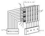
次に、図7は、本発明の有機電界発光素子を用いた平面ディスプレイの構成例である。図示の如く、例えばフルカラーディスプレイの場合は、赤(R)、緑(G)及び青(B)の3原色を発光可能な有機層5(5a,5b,5c,5d)が、陰極3と陽極2との間に配されている。陰極3及び陽極2は、互いに交差するストライプ状に設けることができ、輝度信号回路14及びシフトレジスタ内蔵の制御回路15により選択されて、それぞれに信号電圧が印加され、これによって、選択された陰極3及び陽極2が交差する位置(画素)の有機層が発光するように構成されている。
【0073】
即ち、図7は例えば8×3RGB単純マトリックスであって、正孔輸送層と、発光層及び電子輸送層のいずれか少なくとも一つからなる積層体5を陰極3と陽極2の間に配設したものである(図3又は図4、図5又は図6参照)。陰極と陽極は、ともにストライプ状にパターニングするとともに、互いにマトリックス状に直交させ、シフトレジスタ内蔵の制御回路15及び輝度信号回路14により時系列的に信号電圧を印加し、その交叉位置で発光するように構成されたものである。かかる構成のEL素子は、文字・記号等のディスプレイとしては勿論、画像再生装置としても使用できる。また、陰極3と陽極2のストライプ状パターンを赤(R)、緑(G)、青(B)の各色毎に配し、マルチカラーあるいはフルカラーの全固体型フラットパネルディスプレイを構成することが可能となる。また、上記の単純マトリックス方式のみならず、アクティブマトリックス方式での駆動も可能である。
【0074】
【実施例】
次に、本発明の実施例を示すが、本発明はこれに限定されるものではない。
【0075】
参考例1
この参考例は、下記構造式(18)−1のアミノスチリル化合物と、α−NPD(α−ナフチルフェニルジアミン)との混合層を正孔輸送性発光層として用い、シングルヘテロ構造の下面発光型の有機電界発光素子を作製した例である。
【0076】
【化3】
構造式(18)−1:
まず、真空蒸着装置中に、100nmの厚さのITOからなる陽極が一表面に形成された30mm×30mmのガラス基板をセッティングした。蒸着マスクとして複数の2.0mm×2.0mmの単位開口を有する金属マスクを基板に近接して配置し、真空蒸着法により10-4Pa以下の真空下で上記構造式(18)−1のスチリル化合物と正孔輸送材料であるα−NPDとを重量比1:1で混合した層を例えば50nmの厚さに正孔輸送層(兼発光層)として成膜した。蒸着レートは各々0.1nm/秒とした。
【0078】
さらに、電子輸送層材料として下記構造式のAlq3(トリス(8−キノリノール)アルミニウム)を正孔輸送層に接して蒸着した。Alq3からなるこの電子輸送層の膜厚も例えば50nmとし、蒸着レートは0.2nm/秒とした。
【0079】
【化5】
陰極材料としてはMgとAgの混合膜を採用し、これも蒸着により、例えばMgとAgの混合比を1:3として200nmの厚さに形成し、参考例1による図3に示した如き有機電界発光素子を作製した。
【0081】
このように作製した参考例1の有機電界発光素子に、窒素雰囲気下で順バイアス直流電圧を加えて発光特性を評価した。発光色は赤色であり、分光測定を行った結果、620nm付近に発光ピークを有するスペクトルを得た。分光測定は、大塚電子社製のフォトダイオードアレイを検出器とした分光器を用いた。また、電圧−輝度測定を行ったところ、8Vで1500cd/m2の輝度が得られた。
【0082】
この有機電界発光素子を作製後、窒素雰囲気下に1ヶ月間放置したが、素子劣化は観察されなかった。また、初期輝度300cd/m2で電流値を一定に通電して連続発光し、強制劣化させた際、輝度が半減するまで2500時間であった。
【0083】
参考例2
この参考例は、上記構造式(18)−1のスチリル化合物と、上記構造式のAlq3との混合層を電子輸送性発光層として用い、シングルヘテロ構造の下面発光型の有機電界発光素子を作製した例である。
【0084】
まず、真空蒸着装置中に、100nmの厚さのITOからなる陽極が一表面に形成された30mm×30mmのガラス基板をセッティングした。蒸着マスクとして複数の2.0mm×2.0mmの単位開口を有する金属マスクを基板に近接して配置し、真空蒸着法により10-4Pa以下の真空下で前記構造式のα−NPDを例えば50nmの厚さに成膜した。蒸着レートは0.1nm/秒とした。
【0085】
さらに、上記構造式(18)−1のスチリル化合物と電子輸送性材料であるAlq3とを重量比1:1で混合した層を正孔輸送層に接して蒸着した。上記構造式(18)−1のアミノスチリル化合物とAlq3とからなる電子輸送層(兼発光層)の膜厚も例えば50nmとし、蒸着レートは各々0.2nm/秒とした。
【0086】
陰極材料としてはMgとAgの混合膜を採用し、これも蒸着により、例えばMgとAgの混合比を1:3として200nmの厚さに形成し、参考例2による図3に示した如き有機電界発光素子を作製した。
【0087】
このように作製した参考例2の有機電界発光素子に、窒素雰囲気下で順バイアス直流電圧を加えて発光特性を評価した。発光色は赤色であり、参考例1と同様に分光測定を行った結果、620nm付近に発光ピークを有するスペクトルを得た。また、電圧−輝度測定を行ったところ、8Vで2600cd/m2の輝度が得られた。
【0088】
この有機電界発光素子を作製後、窒素雰囲気下に1ヶ月間放置したが、素子劣化は観察されなかった。また、初期輝度300cd/m2で電流値を一定に通電して連続発光し、強制劣化させた際、輝度が半減するまで2700時間であった。
【0089】
参考例3
この参考例は、上記構造式(18)−1のスチリル化合物と、上記構造式のAlq3との混合層を電子輸送性発光層として用い、ダブルヘテロ構造の下面発光型の有機電界発光素子を作製した例である。
【0090】
まず、真空蒸着装置中に、100nmの厚さのITOからなる陽極が一表面に形成された30mm×30mmのガラス基板をセッティングした。蒸着マスクとして複数の2.0mm×2.0mmの単位開口を有する金属マスクを基板に近接して配置し、真空蒸着法により10-4Pa以下の真空下で上記構造式のα−NPDを例えば30nmの厚さに成膜した。蒸着レートは0.2nm/秒とした。
【0091】
さらに、発光材料として上記構造式(18)−1のスチリル化合物とAlq3とを重量比1:1で正孔輸送層に接して蒸着した。上記構造式(18)−1のスチリル化合物とAlq3との混合層からなる発光層の膜厚も例えば30nmとし、蒸着レートは各々0.2nm/秒とした。
【0092】
さらに、電子輸送性材料として上記構造式のAlq3を発光層に接して蒸着した。Alq3の膜厚を例えば30nmとし、蒸着レートは0.2nm/秒とした。
【0093】
陰極材料としてはMgとAgの混合膜を採用し、これも蒸着により、例えばMgとAgの混合比を1:3として200nmの厚さに形成し、参考例3による図4に示した如き有機電界発光素子を作製した。
【0094】
このように作製した参考例3の有機電界発光素子に、窒素雰囲気下で順バイアス直流電圧を加えて発光特性を評価した。発光色は赤色であり、参考例1と同様に分光測定を行った結果、620nmに発光ピークを有するスペクトルを得た。また、電圧−輝度測定を行ったところ、8Vで3200cd/m2の輝度が得られた。
【0095】
この有機電界発光素子を作製後、窒素雰囲気下に1ヶ月間放置したが、素子劣化は観察されなかった。また、初期輝度300cd/m2で電流値を一定に通電して連続発光して強制劣化させた際、輝度が半減するまで3500時間であった。
【0096】
参考例4
この参考例は、上記構造式(18)−1のスチリル化合物と、下記構造式(18)−2のスチリル化合物との混合層を発光層として用い、ダブルヘテロ構造の下面発光型の有機電界発光素子を作製した例である。
【0097】
【化6】
構造式(18)−2:
まず、真空蒸着装置中に、100nmの厚さのITOからなる陽極が一表面に形成された30mm×30mmのガラス基板をセッティングした。蒸着マスクとして複数の2.0mm×2.0mmの単位開口を有する金属マスクを基板に近接して配置し、真空蒸着法により10-4Pa以下の真空下で上記構造式のα−NPDを例えば30nmの厚さに成膜した。蒸着レートは0.2nm/秒とした。
【0099】
さらに、発光材料として上記構造式(18)−1のスチリル化合物と上記構造式((18)−2のスチリル化合物とを重量比1:3で正孔輸送層に接して共蒸着した。上記構造式(18)−1のスチリル化合物と上記構造式(18)−2のスチリル化合物との混合層からなる発光層の膜厚も例えば30nmとし、蒸着レートは上記構造式(18)−1の化合物は0.1nm/秒、上記構造式(18)−2の化合物は0.3nm/秒とした。
【0100】
さらに、電子輸送性材料として上記構造式のAlq3を発光層に接して蒸着した。Alq3の膜厚を例えば30nmとし、蒸着レートは0.2nm/秒とした。
【0101】
陰極材料としてはMgとAgの混合膜を採用し、これも蒸着により、例えばMgとAgの混合比を1:3として200nmの厚さに形成し、参考例4による図4に示した如き有機電界発光素子を作製した。
【0102】
このように作製した参考例4の有機電界発光素子に、窒素雰囲気下で順バイアス直流電圧を加えて発光特性を評価した。発光色は橙色であり、参考例1と同様に分光測定を行った結果、610nmに発光ピークを有するスペクトルを得た。電圧−輝度測定を行ったところ、8Vで2200cd/m2の輝度が得られた。
【0103】
この有機電界発光素子を作製後、窒素雰囲気下に1ヶ月間放置したが、素子劣化は観察されなかった。また、初期輝度300cd/m2で電流値を一定に通電して連続発光して強制劣化させた際、輝度が半減するまで1000時間であった。
【0104】
参考例5
この参考例は、上記構造式(18)−1のスチリル化合物と、上記構造式のAlq3との混合層を電子輸送性発光層として用い、シングルヘテロ構造の下面発光型の有機電界発光素子を作製した例である。
【0105】
層構造、成膜法とも参考例2に準拠して有機電界発光素子を作製した。
【0106】
このように作製した参考例5の有機電界発光素子に、窒素雰囲気下で順バイアス直流電圧を加えて発光特性を評価した。発光色は橙色であり、参考例1と同様に分光測定を行った結果、608nm付近に発光ピークを有するスペクトルを得た。また、電圧−輝度測定を行ったところ、8Vで1000cd/m2の輝度が得られた。
【0107】
この有機電界発光素子を作製後、窒素雰囲気下に1ヶ月間放置したが、素子劣化は観察されなかった。また、初期輝度300cd/m2で電流値を一定に通電して連続発光し、強制劣化させた際、輝度が半減するまで800時間であった。
【0108】
参考例6
この参考例は、下記構造式(18)−3のスチリル化合物と、上記構造式のAlq3との混合層を電子輸送性発光層として用い、シングルヘテロ構造の下面発光型の有機電界発光素子を作製した例である。
【0109】
【化7】
構造式(18)−3:
層構造、成膜法とも参考例2に準拠して有機電界発光素子を作製した。
【0111】
このように作製した参考例6の有機電界発光素子に、窒素雰囲気下で順バイアス直流電圧を加えて発光特性を評価した。発光色は橙色であり、参考例1と同様に分光測定を行った結果、610nm付近に発光ピークを有するスペクトルを得た。また、電圧−輝度測定を行ったところ、8Vで500cd/m2の輝度が得られた。
【0112】
この有機電界発光素子を作製後、窒素雰囲気下に1ヶ月間放置したが、素子劣化は観察されなかった。また、初期輝度300cd/m2で電流値を一定に通電して連続発光し、強制劣化させた際、輝度が半減するまで700時間であった。
【0113】
参考例7
この参考例は、下記構造式(18)−4のスチリル化合物と、上記構造式のAlq3との混合層を電子輸送性発光層として用い、シングルヘテロ構造の下面発光型の有機電界発光素子を作製した例である。
【0114】
【化8】
構造式(18)−4:
層構造、成膜法とも参考例2に準拠して有機電界発光素子を作製した。
【0116】
このように作製した参考例7の有機電界発光素子に、窒素雰囲気下で順バイアス直流電圧を加えて発光特性を評価した。発光色は橙色であり、参考例1と同様に分光測定を行った結果、605nm付近に発光ピークを有するスペクトルを得た。また、電圧−輝度測定を行ったところ、8Vで1200cd/m2の輝度が得られた。
【0117】
この有機電界発光素子を作製後、窒素雰囲気下に1ヶ月間放置したが、素子劣化は観察されなかった。また、初期輝度300cd/m2で電流値を一定に通電して連続発光し、強制劣化させた際、輝度が半減するまで1100時間であった。
【0118】
実施例1
本実施例は、下記構造式(17)−1のスチリル化合物と、上記構造式のAlq3との混合層を電子輸送性発光層として用い、シングルヘテロ構造の下面発光型の有機電界発光素子を作製した例である。
【0119】
【化9】
構造式(17)−1:
層構造、成膜法とも参考例2に準拠して有機電界発光素子を作製した。
【0121】
このように作製した実施例1の有機電界発光素子に、窒素雰囲気下で順バイアス直流電圧を加えて発光特性を評価した。発光色は橙色であり、参考例1と同様に分光測定を行った結果、600nm付近に発光ピークを有するスペクトルを得た。また、電圧−輝度測定を行ったところ、8Vで1000cd/m2の輝度が得られた。
【0122】
この有機電界発光素子を作製後、窒素雰囲気下に1ヶ月間放置したが、素子劣化は観察されなかった。また、初期輝度300cd/m2で電流値を一定に通電して連続発光し、強制劣化させた際、輝度が半減するまで1400時間であった。
【0123】
参考例8
この参考例は、下記構造式(18)−5のスチリル化合物と、上記構造式のAlq3との混合層を電子輸送性発光層として用い、シングルヘテロ構造の下面発光型の有機電界発光素子を作製した例である。
【0124】
【化10】
構造式(18)−5:
層構造、成膜法とも参考例2に準拠して有機電界発光素子を作製した。
【0126】
このように作製した参考例8の有機電界発光素子に、窒素雰囲気下で順バイアス直流電圧を加えて発光特性を評価した。発光色は橙色であり、参考例1と同様に分光測定を行った結果、615nm付近に発光ピークを有するスペクトルを得た。また、電圧−輝度測定を行ったところ、8Vで900cd/m2の輝度が得られた。
【0127】
この有機電界発光素子を作製後、窒素雰囲気下に1ヶ月間放置したが、素子劣化は観察されなかった。また、初期輝度300cd/m2で電流値を一定に通電して連続発光し、強制劣化させた際、輝度が半減するまで850時間であった。
【0128】
参考例9
この参考例は、下記構造式(18)−6のスチリル化合物と、上記構造式のAlq3との混合層を電子輸送性発光層として用い、シングルヘテロ構造の下面発光型の有機電界発光素子を作製した例である。
【0129】
【化11】
構造式(18)−6:
層構造、成膜法とも参考例2に準拠して有機電界発光素子を作製した。
【0131】
このように作製した参考例9の有機電界発光素子に、窒素雰囲気下で順バイアス直流電圧を加えて発光特性を評価した。発光色は赤色であり、参考例1と同様に分光測定を行った結果、620nm付近に発光ピークを有するスペクトルを得た。また、電圧−輝度測定を行ったところ、8Vで800cd/m2の輝度が得られた。
【0132】
この有機電界発光素子を作製後、窒素雰囲気下に1ヶ月間放置したが、素子劣化は観察されなかった。また、初期輝度300cd/m2で電流値を一定に通電して連続発光し、強制劣化させた際、輝度が半減するまで700時間であった。
【0133】
参考例10
この参考例は、下記構造式(18)−7のスチリル化合物と、上記構造式のAlq3との混合層を電子輸送性発光層として用い、シングルヘテロ構造の下面発光型の有機電界発光素子を作製した例である。
【0134】
【化12】
構造式(18)−7:
層構造、成膜法とも参考例2に準拠して有機電界発光素子を作製した。
【0136】
このように作製した参考例10の有機電界発光素子に、窒素雰囲気下で順バイアス直流電圧を加えて発光特性を評価した。発光色は橙色であり、参考例1と同様に分光測定を行った結果、615nm付近に発光ピークを有するスペクトルを得た。また、電圧−輝度測定を行ったところ、8Vで1100cd/m2の輝度が得られた。
【0137】
この有機電界発光素子を作製後、窒素雰囲気下に1ヶ月間放置したが、素子劣化は観察されなかった。また、初期輝度300cd/m2で電流値を一定に通電して連続発光し、強制劣化させた際、輝度が半減するまで1000時間であった。
【0138】
実施例2
本実施例は、下記構造式(17)−2のスチリル化合物と、上記構造式のAlq3との混合層を電子輸送性発光層として用い、シングルヘテロ構造の下面発光型の有機電界発光素子を作製した例である。
【0139】
【化13】
構造式(17)−2:
層構造、成膜法とも参考例2に準拠して有機電界発光素子を作製した。
【0141】
このように作製した実施例2の有機電界発光素子に、窒素雰囲気下で順バイアス直流電圧を加えて発光特性を評価した。発光色は橙色であり、参考例1と同様に分光測定を行った結果、610nm付近に発光ピークを有するスペクトルを得た。また、電圧−輝度測定を行ったところ、8Vで950cd/m2の輝度が得られた。
【0142】
この有機電界発光素子を作製後、窒素雰囲気下に1ヶ月間放置したが、素子劣化は観察されなかった。また、初期輝度300cd/m2で電流値を一定に通電して連続発光し、強制劣化させた際、輝度が半減するまで1300時間であった。
【0143】
参考例11
この参考例は、下記構造式(18)−8のスチリル化合物と、上記構造式のAlq3との混合層を電子輸送性発光層として用い、シングルヘテロ構造の下面発光型の有機電界発光素子を作製した例である。
【0144】
【化14】
構造式(18)−8:
層構造、成膜法とも参考例2に準拠して有機電界発光素子を作製した。
【0146】
このように作製した参考例11の有機電界発光素子に、窒素雰囲気下で順バイアス直流電圧を加えて発光特性を評価した。発光色は橙色であり、参考例1と同様に分光測定を行った結果、605nm付近に発光ピークを有するスペクトルを得た。また、電圧−輝度測定を行ったところ、8Vで850cd/m2の輝度が得られた。
【0147】
この有機電界発光素子を作製後、窒素雰囲気下に1ヶ月間放置したが、素子劣化は観察されなかった。また、初期輝度300cd/m2で電流値を一定に通電して連続発光し、強制劣化させた際、輝度が半減するまで650時間であった。
【0148】
参考例12
この参考例は、下記構造式(18)−9のスチリル化合物と、上記構造式のAlq3との混合層を電子輸送性発光層として用い、シングルヘテロ構造の下面発光型の有機電界発光素子を作製した例である。
【0149】
【化15】
構造式(18)−9:
層構造、成膜法とも参考例2に準拠して有機電界発光素子を作製した。
【0151】
このように作製した参考例12の有機電界発光素子に、窒素雰囲気下で順バイアス直流電圧を加えて発光特性を評価した。発光色は橙色であり、参考例1と同様に分光測定を行った結果、610nm付近に発光ピークを有するスペクトルを得た。また、電圧−輝度測定を行ったところ、8Vで750cd/m2の輝度が得られた。
【0152】
この有機電界発光素子を作製後、窒素雰囲気下に1ヶ月間放置したが、素子劣化は観察されなかった。また、初期輝度300cd/m2で電流値を一定に通電して連続発光し、強制劣化させた際、輝度が半減するまで500時間であった。
【0153】
参考例13
この参考例は、下記構造式(18)−10のスチリル化合物と、上記構造式のAlq3との混合層を電子輸送性発光層として用い、シングルヘテロ構造の下面発光型の有機電界発光素子を作製した例である。
【0154】
【化16】
構造式(18)−10:
層構造、成膜法とも参考例2に準拠して有機電界発光素子を作製した。
【0156】
このように作製した参考例13の有機電界発光素子に、窒素雰囲気下で順バイアス直流電圧を加えて発光特性を評価した。発光色は赤色であり、参考例1と同様に分光測定を行った結果、625nm付近に発光ピークを有するスペクトルを得た。また、電圧−輝度測定を行ったところ、8Vで1000cd/m2の輝度が得られた。
【0157】
この有機電界発光素子を作製後、窒素雰囲気下に1ヶ月間放置したが、素子劣化は観察されなかった。また、初期輝度300cd/m2で電流値を一定に通電して連続発光し、強制劣化させた際、輝度が半減するまで1500時間であった。
【0158】
参考例14
この参考例は、下記構造式(18)−11のスチリル化合物と、上記構造式のAlq3との混合層を電子輸送性発光層として用い、シングルヘテロ構造の下面発光型の有機電界発光素子を作製した例である。
【0159】
【化17】
構造式(18)−11:
層構造、成膜法とも参考例2に準拠して有機電界発光素子を作製した。
【0161】
このように作製した参考例14の有機電界発光素子に、窒素雰囲気下で順バイアス直流電圧を加えて発光特性を評価した。発光色は橙色であり、参考例1と同様に分光測定を行った結果、610nm付近に発光ピークを有するスペクトルを得た。また、電圧−輝度測定を行ったところ、8Vで2000cd/m2の輝度が得られた。
【0162】
この有機電界発光素子を作製後、窒素雰囲気下に1ヶ月間放置したが、素子劣化は観察されなかった。また、初期輝度300cd/m2で電流値を一定に通電して連続発光し、強制劣化させた際、輝度が半減するまで2800時間であった。
【0163】
実施例3
本実施例は、下記構造式(17)−3のスチリル化合物と、上記構造式のAlq3との混合層を電子輸送性発光層として用い、シングルヘテロ構造の下面発光型の有機電界発光素子を作製した例である。
【0164】
【化18】
構造式(17)−3:
層構造、成膜法とも参考例2に準拠して有機電界発光素子を作製した。
【0166】
このように作製した実施例3の有機電界発光素子に、窒素雰囲気下で順バイアス直流電圧を加えて発光特性を評価した。発光色は橙色であり、参考例1と同様に分光測定を行った結果、605nm付近に発光ピークを有するスペクトルを得た。また、電圧−輝度測定を行ったところ、8Vで1800cd/m2の輝度が得られた。
【0167】
この有機電界発光素子を作製後、窒素雰囲気下に1ヶ月間放置したが、素子劣化は観察されなかった。また、初期輝度300cd/m2で電流値を一定に通電して連続発光し、強制劣化させた際、輝度が半減するまで3300時間であった。
【0168】
参考例15
この参考例は、下記構造式(18)−12のスチリル化合物と、上記構造式のAlq3との混合層を電子輸送性発光層として用い、シングルヘテロ構造の下面発光型の有機電界発光素子を作製した例である。
【0169】
【化19】
構造式(18)−12:
層構造、成膜法とも参考例2に準拠して有機電界発光素子を作製した。
【0171】
このように作製した参考例15の有機電界発光素子に、窒素雰囲気下で順バイアス直流電圧を加えて発光特性を評価した。発光色は橙色であり、参考例1と同様に分光測定を行った結果、605nm付近に発光ピークを有するスペクトルを得た。また、電圧−輝度測定を行ったところ、8Vで880cd/m2の輝度が得られた。
【0172】
この有機電界発光素子を作製後、窒素雰囲気下に1ヶ月間放置したが、素子劣化は観察されなかった。また、初期輝度300cd/m2で電流値を一定に通電して連続発光し、強制劣化させた際、輝度が半減するまで700時間であった。
【0173】
実施例4
本実施例は、下記構造式(17)−4のスチリル化合物と、上記構造式のAlq3との混合層を電子輸送性発光層として用い、シングルヘテロ構造の下面発光型の有機電界発光素子を作製した例である。
【0174】
【化20】
構造式(17)−4:
層構造、成膜法とも参考例2に準拠して有機電界発光素子を作製した。
【0176】
このように作製した実施例4の有機電界発光素子に、窒素雰囲気下で順バイアス直流電圧を加えて発光特性を評価した。発光色は橙色であり、参考例1と同様に分光測定を行った結果、605nm付近に発光ピークを有するスペクトルを得た。また、電圧−輝度測定を行ったところ、8Vで900cd/m2の輝度が得られた。
【0177】
この有機電界発光素子を作製後、窒素雰囲気下に1ヶ月間放置したが、素子劣化は観察されなかった。また、初期輝度300cd/m2で電流値を一定に通電して連続発光し、強制劣化させた際、輝度が半減するまで850時間であった。
【0178】
参考例16
この参考例は、下記構造式(18)−13のスチリル化合物と、上記構造式のAlq3との混合層を電子輸送性発光層として用い、シングルヘテロ構造の下面発光型の有機電界発光素子を作製した例である。
【0179】
【化21】
構造式(18)−13:
層構造、成膜法とも参考例2に準拠して有機電界発光素子を作製した。
【0181】
このように作製した参考例16の有機電界発光素子に、窒素雰囲気下で順バイアス直流電圧を加えて発光特性を評価した。発光色は赤色であり、参考例1と同様に分光測定を行った結果、700nm付近に発光ピークを有するスペクトルを得た。また、電圧−輝度測定を行ったところ、8Vで250cd/m2の輝度が得られた。
【0182】
この有機電界発光素子を作製後、窒素雰囲気下に1ヶ月間放置したが、素子劣化は観察されなかった。また、初期輝度300cd/m2で電流値を一定に通電して連続発光し、強制劣化させた際、輝度が半減するまで350時間であった。
【0183】
実施例5
本実施例は、下記構造式(17)−5のスチリル化合物と、上記構造式のAlq3との混合層を電子輸送性発光層として用い、シングルヘテロ構造の下面発光型の有機電界発光素子を作製した例である。
【0184】
【化22】
構造式(17)−5:
層構造、成膜法とも参考例2に準拠して有機電界発光素子を作製した。
【0186】
このように作製した実施例5の有機電界発光素子に、窒素雰囲気下で順バイアス直流電圧を加えて発光特性を評価した。発光色は赤色であり、参考例1と同様に分光測定を行った結果、690nm付近に発光ピークを有するスペクトルを得た。また、電圧−輝度測定を行ったところ、8Vで180cd/m2の輝度が得られた。
【0187】
この有機電界発光素子を作製後、窒素雰囲気下に1ヶ月間放置したが、素子劣化は観察されなかった。また、初期輝度300cd/m2で電流値を一定に通電して連続発光し、強制劣化させた際、輝度が半減するまで450時間であった。
【0188】
参考例17
この参考例は、下記構造式(18)−14のスチリル化合物と、上記構造式のAlq3との混合層を電子輸送性発光層として用い、シングルヘテロ構造の下面発光型の有機電界発光素子を作製した例である。
【0189】
【化23】
構造式(18)−14:
層構造、成膜法とも参考例2に準拠して有機電界発光素子を作製した。
【0191】
このように作製した参考例17の有機電界発光素子に、窒素雰囲気下で順バイアス直流電圧を加えて発光特性を評価した。発光色は赤色であり、参考例1と同様に分光測定を行った結果、690nm付近に発光ピークを有するスペクトルを得た。また、電圧−輝度測定を行ったところ、8Vで330cd/m2の輝度が得られた。
【0192】
この有機電界発光素子を作製後、窒素雰囲気下に1ヶ月間放置したが、素子劣化は観察されなかった。また、初期輝度300cd/m2で電流値を一定に通電して連続発光し、強制劣化させた際、輝度が半減するまで390時間であった。
【0193】
実施例6
本実施例は、下記構造式(17)−6のスチリル化合物と、上記構造式のAlq3との混合層を電子輸送性発光層として用い、シングルヘテロ構造の下面発光型の有機電界発光素子を作製した例である。
【0194】
【化24】
構造式(17)−6:
層構造、成膜法とも参考例2に準拠して有機電界発光素子を作製した。
【0196】
このように作製した実施例6の有機電界発光素子に、窒素雰囲気下で順バイアス直流電圧を加えて発光特性を評価した。発光色は赤色であり、参考例1と同様に分光測定を行った結果、680nm付近に発光ピークを有するスペクトルを得た。また、電圧−輝度測定を行ったところ、8Vで280cd/m2の輝度が得られた。
【0197】
この有機電界発光素子を作製後、窒素雰囲気下に1ヶ月間放置したが、素子劣化は観察されなかった。また、初期輝度300cd/m2で電流値を一定に通電して連続発光し、強制劣化させた際、輝度が半減するまで500時間であった。
【0198】
参考例18
この参考例は、下記構造式(18)−15のスチリル化合物と、上記構造式Alq3との混合層を電子輸送性発光層として用い、シングルヘテロ構造の下面発光型の有機電界発光素子を作製した例である。
【0199】
【化25】
構造式(18)−15:
層構造、成膜法とも参考例2に準拠して有機電界発光素子を作製した。
【0201】
このように作製した参考例18の有機電界発光素子に、窒素雰囲気下で順バイアス直流電圧を加えて発光特性を評価した。発光色は赤色であり、参考例1と同様に分光測定を行った結果、680nm付近に発光ピークを有するスペクトルを得た。また、電圧−輝度測定を行ったところ、8Vで220cd/m2の輝度が得られた。
【0202】
この有機電界発光素子を作製後、窒素雰囲気下に1ヶ月間放置したが、素子劣化は観察されなかった。また、初期輝度300cd/m2で電流値を一定に通電して連続発光し、強制劣化させた際、輝度が半減するまで210時間であった。
【0203】
実施例7
本実施例は、下記構造式(17)−7のスチリル化合物と、上記構造式のAlq3との混合層を電子輸送性発光層として用い、シングルヘテロ構造の下面発光型の有機電界発光素子を作製した例である。
【0204】
【化26】
構造式(17)−7:
層構造、成膜法とも参考例2に準拠して有機電界発光素子を作製した。
【0206】
このように作製した実施例7の有機電界発光素子に、窒素雰囲気下で順バイアス直流電圧を加えて発光特性を評価した。発光色は赤色であり、参考例1と同様に分光測定を行った結果、675nm付近に発光ピークを有するスペクトルを得た。また、電圧−輝度測定を行ったところ、8Vで240cd/m2の輝度が得られた。
【0207】
この有機電界発光素子を作製後、窒素雰囲気下に1ヶ月間放置したが、素子劣化は観察されなかった。また、初期輝度300cd/m2で電流値を一定に通電して連続発光し、強制劣化させた際、輝度が半減するまで240時間であった。
【0208】
実施例8
本実施例は、下記構造式(17)−8のスチリル化合物と、上記構造式のAlq3との混合層を電子輸送性発光層として用い、シングルヘテロ構造の下面発光型の有機電界発光素子を作製した例である。
【0209】
【化27】
構造式(17)−8:
層構造、成膜法とも参考例2に準拠して有機電界発光素子を作製した。
【0211】
このように作製した実施例8の有機電界発光素子に、窒素雰囲気下で順バイアス直流電圧を加えて発光特性を評価した。発光色は赤色であり、参考例1と同様に分光測定を行った結果、680nm付近に発光ピークを有するスペクトルを得た。また、電圧−輝度測定を行ったところ、8Vで260cd/m2の輝度が得られた。
【0212】
この有機電界発光素子を作製後、窒素雰囲気下に1ヶ月間放置したが、素子劣化は観察されなかった。また、初期輝度300cd/m2で電流値を一定に通電して連続発光し、強制劣化させた際、輝度が半減するまで320時間であった。
【0213】
実施例9
本実施例は、下記構造式(17)−9のスチリル化合物と、上記構造式のAlq3との混合層を電子輸送性発光層として用い、シングルヘテロ構造の下面発光型の有機電界発光素子を作製した例である。
【0214】
【化28】
構造式(17)−9:
層構造、成膜法とも参考例2に準拠して有機電界発光素子を作製した。
【0216】
このように作製した実施例9の有機電界発光素子に、窒素雰囲気下で順バイアス直流電圧を加えて発光特性を評価した。発光色は赤色であり、参考例1と同様に分光測定を行った結果、680nm付近に発光ピークを有するスペクトルを得た。また、電圧−輝度測定を行ったところ、8Vで180cd/m2の輝度が得られた。
【0217】
この有機電界発光素子を作製後、窒素雰囲気下に1ヶ月間放置したが、素子劣化は観察されなかった。また、初期輝度300cd/m2で電流値を一定に通電して連続発光し、強制劣化させた際、輝度が半減するまで280時間であった。
【0218】
実施例10
本実施例は、下記構造式(17)−10のスチリル化合物と、上記構造式のAlq3との混合層を電子輸送性発光層として用い、シングルヘテロ構造の下面発光型の有機電界発光素子を作製した例である。
【0219】
【化29】
構造式(17)−10:
層構造、成膜法とも参考例2に準拠して有機電界発光素子を作製した。
【0221】
このように作製した実施例10の有機電界発光素子に、窒素雰囲気下で順バイアス直流電圧を加えて発光特性を評価した。発光色は赤色であり、参考例1と同様に分光測定を行った結果、675nm付近に発光ピークを有するスペクトルを得た。また、電圧−輝度測定を行ったところ、8Vで340cd/m2の輝度が得られた。
【0222】
この有機電界発光素子を作製後、窒素雰囲気下に1ヶ月間放置したが、素子劣化は観察されなかった。また、初期輝度300cd/m2で電流値を一定に通電して連続発光し、強制劣化させた際、輝度が半減するまで600時間であった。
【0223】
実施例11
本実施例は、下記構造式(17)−11のスチリル化合物と、上記構造式Alq3との混合層を電子輸送性発光層として用い、シングルヘテロ構造の下面発光型の有機電界発光素子を作製した例である。
【0224】
【化30】
構造式(17)−11:
層構造、成膜法とも参考例2に準拠して有機電界発光素子を作製した。
【0226】
このように作製した実施例11の有機電界発光素子に、窒素雰囲気下で順バイアス直流電圧を加えて発光特性を評価した。発光色は赤色であり、参考例1と同様に分光測定を行った結果、630nm付近に発光ピークを有するスペクトルを得た。また、電圧−輝度測定を行ったところ、8Vで550cd/m2の輝度が得られた。
【0227】
この有機電界発光素子を作製後、窒素雰囲気下に1ヶ月間放置したが、素子劣化は観察されなかった。また、初期輝度300cd/m2で電流値を一定に通電して連続発光し、強制劣化させた際、輝度が半減するまで780時間であった。
【0228】
実施例12
本実施例は、下記構造式(17)−12のスチリル化合物と、上記構造式のAlq3との混合層を電子輸送性発光層として用い、シングルヘテロ構造の下面発光型の有機電界発光素子を作製した例である。
【0229】
【化31】
構造式(17)−12:
層構造、成膜法とも参考例2に準拠して有機電界発光素子を作製した。
【0231】
このように作製した実施例12の有機電界発光素子に、窒素雰囲気下で順バイアス直流電圧を加えて発光特性を評価した。発光色は赤色であり、参考例1と同様に分光測定を行った結果、640nm付近に発光ピークを有するスペクトルを得た。また、電圧−輝度測定を行ったところ、8Vで700cd/m2の輝度が得られた。
【0232】
この有機電界発光素子を作製後、窒素雰囲気下に1ヶ月間放置したが、素子劣化は観察されなかった。また、初期輝度300cd/m2で電流値を一定に通電して連続発光し、強制劣化させた際、輝度が半減するまで1500時間であった。
【0233】
実施例13
本実施例は、下記構造式(17)−13のスチリル化合物と、上記構造式のAlq3との混合層を電子輸送性発光層として用い、シングルヘテロ構造の下面発光型の有機電界発光素子を作製した例である。
【0234】
【化32】
構造式(17)−13:
層構造、成膜法とも参考例2に準拠して有機電界発光素子を作製した。
【0236】
このように作製した実施例13の有機電界発光素子に、窒素雰囲気下で順バイアス直流電圧を加えて発光特性を評価した。発光色は赤色であり、参考例1と同様に分光測定を行った結果、645nm付近に発光ピークを有するスペクトルを得た。また、電圧−輝度測定を行ったところ、8Vで720cd/m2の輝度が得られた。
【0237】
この有機電界発光素子を作製後、窒素雰囲気下に1ヶ月間放置したが、素子劣化は観察されなかった。また、初期輝度300cd/m2で電流値を一定に通電して連続発光し、強制劣化させた際、輝度が半減するまで2200時間であった。
【0238】
実施例14
本実施例は、下記構造式(17)−14のスチリル化合物と、上記の構造式のAlq3との混合層を電子輸送性発光層として用い、シングルヘテロ構造の下面発光型の有機電界発光素子を作製した例である。
【0239】
【化33】
構造式(17)−14:
層構造、成膜法とも参考例2に準拠して有機電界発光素子を作製した。
【0241】
このように作製した実施例14の有機電界発光素子に、窒素雰囲気下で順バイアス直流電圧を加えて発光特性を評価した。発光色は赤色であり、参考例1と同様に分光測定を行った結果、648nm付近に発光ピークを有するスペクトルを得た。また、電圧−輝度測定を行ったところ、8Vで750cd/m2の輝度が得られた。
【0242】
この有機電界発光素子を作製後、窒素雰囲気下に1ヶ月間放置したが、素子劣化は観察されなかった。また、初期輝度300cd/m2で電流値を一定に通電して連続発光し、強制劣化させた際、輝度が半減するまで3200時間であった。
【0243】
実施例15
本実施例は、下記構造式(17)−15のスチリル化合物と、上記構造式のAlq3との混合層を電子輸送性発光層として用い、シングルヘテロ構造の下面発光型の有機電界発光素子を作製した例である。
【0244】
【化34】
構造式(17)−15:
層構造、成膜法とも参考例2に準拠して有機電界発光素子を作製した。
【0246】
このように作製した実施例15の有機電界発光素子に、窒素雰囲気下で順バイアス直流電圧を加えて発光特性を評価した。発光色は赤色であり、参考例1と同様に分光測定を行った結果、665nm付近に発光ピークを有するスペクトルを得た。また、電圧−輝度測定を行ったところ、8Vで850cd/m2の輝度が得られた。
【0247】
この有機電界発光素子を作製後、窒素雰囲気下に1ヶ月間放置したが、素子劣化は観察されなかった。また、初期輝度300cd/m2で電流値を一定に通電して連続発光し、強制劣化させた際、輝度が半減するまで2500時間であった。
【0248】
実施例16
本実施例は、下記構造式(17)−16のスチリル化合物と、上記構造式のAlq3との混合層を電子輸送性発光層として用い、シングルヘテロ構造の下面発光型の有機電界発光素子を作製した例である。
【0249】
【化35】
構造式(17)−16:
層構造、成膜法とも参考例2に準拠して有機電界発光素子を作製した。
【0251】
このように作製した実施例16の有機電界発光素子に、窒素雰囲気下で順バイアス直流電圧を加えて発光特性を評価した。発光色は赤色であり、参考例1と同様に分光測定を行った結果、638nm付近に発光ピークを有するスペクトルを得た。また、電圧−輝度測定を行ったところ、8Vで1200cd/m2の輝度が得られた。
【0252】
この有機電界発光素子を作製後、窒素雰囲気下に1ヶ月間放置したが、素子劣化は観察されなかった。また、初期輝度300cd/m2で電流値を一定に通電して連続発光し、強制劣化させた際、輝度が半減するまで5000時間であった。
【0253】
実施例17
本実施例は、下記構造式(17)−17のスチリル化合物と、上記構造式のAlq3との混合層を電子輸送性発光層として用い、シングルヘテロ構造の下面発光型の有機電界発光素子を作製した例である。
【0254】
【化36】
構造式(17)−17:
層構造、成膜法とも参考例2に準拠して有機電界発光素子を作製した。
【0256】
このように作製した実施例17の有機電界発光素子に、窒素雰囲気下で順バイアス直流電圧を加えて発光特性を評価した。発光色は赤色であり、参考例1と同様に分光測定を行った結果、640nm付近に発光ピークを有するスペクトルを得た。また、電圧−輝度測定を行ったところ、8Vで1150cd/m2の輝度が得られた。
【0257】
この有機電界発光素子を作製後、窒素雰囲気下に1ヶ月間放置したが、素子劣化は観察されなかった。また、初期輝度300cd/m2で電流値を一定に通電して連続発光し、強制劣化させた際、輝度が半減するまで5500時間であった。
【0258】
実施例18
本実施例は、下記構造式(17)−18のスチリル化合物と、上記構造式のAlq3との混合層を電子輸送性発光層として用い、シングルヘテロ構造の下面発光型の有機電界発光素子を作製した例である。
【0259】
【化37】
構造式(17)−18:
層構造、成膜法とも参考例2に準拠して有機電界発光素子を作製した。
【0261】
このように作製した実施例18の有機電界発光素子に、窒素雰囲気下で順バイアス直流電圧を加えて発光特性を評価した。発光色は赤色であり、参考例1と同様に分光測定を行った結果、645nm付近に発光ピークを有するスペクトルを得た。また、電圧−輝度測定を行ったところ、8Vで1180cd/m2の輝度が得られた。
【0262】
この有機電界発光素子を作製後、窒素雰囲気下に1ヶ月間放置したが、素子劣化は観察されなかった。また、初期輝度300cd/m2で電流値を一定に通電して連続発光し、強制劣化させた際、輝度が半減するまで4800時間であった。
【0263】
実施例19
本実施例は、下記構造式(17)−19のスチリル化合物と、上記構造式のAlq3との混合層を電子輸送性発光層として用い、シングルヘテロ構造の下面発光型の有機電界発光素子を作製した例である。
【0264】
【化38】
構造式(17)−19:
層構造、成膜法とも参考例2に準拠して有機電界発光素子を作製した。
【0266】
このように作製した実施例19の有機電界発光素子に、窒素雰囲気下で順バイアス直流電圧を加えて発光特性を評価した。発光色は赤色であり、参考例1と同様に分光測定を行った結果、647nm付近に発光ピークを有するスペクトルを得た。また、電圧−輝度測定を行ったところ、8Vで950cd/m2の輝度が得られた。
【0267】
この有機電界発光素子を作製後、窒素雰囲気下に1ヶ月間放置したが、素子劣化は観察されなかった。また、初期輝度300cd/m2で電流値を一定に通電して連続発光し、強制劣化させた際、輝度が半減するまで5100時間であった。
【0268】
実施例20
本実施例は、下記構造式(17)−20のスチリル化合物と、上記構造式のAlq3との混合層を電子輸送性発光層として用い、シングルヘテロ構造の下面発光型の有機電界発光素子を作製した例である。
【0269】
【化39】
構造式(17)−20:
層構造、成膜法とも参考例2に準拠して有機電界発光素子を作製した。
【0271】
このように作製した実施例20の有機電界発光素子に、窒素雰囲気下で順バイアス直流電圧を加えて発光特性を評価した。発光色は赤色であり、参考例1と同様に分光測定を行った結果、632nm付近に発光ピークを有するスペクトルを得た。また、電圧−輝度測定を行ったところ、8Vで890cd/m2の輝度が得られた。
【0272】
この有機電界発光素子を作製後、窒素雰囲気下に1ヶ月間放置したが、素子劣化は観察されなかった。また、初期輝度300cd/m2で電流値を一定に通電して連続発光し、強制劣化させた際、輝度が半減するまで1500時間であった。
【0273】
実施例21
本実施例は、下記構造式(17)−21のスチリル化合物と、上記構造式のAlq3との混合層を電子輸送性発光層として用い、シングルヘテロ構造の下面発光型の有機電界発光素子を作製した例である。
【0274】
【化40】
構造式(17)−21:
層構造、成膜法とも参考例2に準拠して有機電界発光素子を作製した。
【0276】
このように作製した実施例21の有機電界発光素子に、窒素雰囲気下で順バイアス直流電圧を加えて発光特性を評価した。発光色は橙色であり、参考例1と同様に分光測定を行った結果、585nm付近に発光ピークを有するスペクトルを得た。また、電圧−輝度測定を行ったところ、8Vで300cd/m2の輝度が得られた。
【0277】
この有機電界発光素子を作製後、窒素雰囲気下に1ヶ月間放置したが、素子劣化は観察されなかった。また、初期輝度300cd/m2で電流値を一定に通電して連続発光し、強制劣化させた際、輝度が半減するまで850時間であった。
【0278】
実施例22
本実施例は、下記構造式(17)−22のスチリル化合物と、上記構造式のAlq3との混合層を電子輸送性発光層として用い、シングルヘテロ構造の下面発光型の有機電界発光素子を作製した例である。
【0279】
【化41】
構造式(17)−22:
層構造、成膜法とも参考例2に準拠して有機電界発光素子を作製した。
【0281】
このように作製した実施例22の有機電界発光素子に、窒素雰囲気下で順バイアス直流電圧を加えて発光特性を評価した。発光色は橙色であり、参考例1と同様に分光測定を行った結果、580nm付近に発光ピークを有するスペクトルを得た。また、電圧−輝度測定を行ったところ、8Vで580cd/m2の輝度が得られた。
【0282】
この有機電界発光素子を作製後、窒素雰囲気下に1ヶ月間放置したが、素子劣化は観察されなかった。また、初期輝度300cd/m2で電流値を一定に通電して連続発光し、強制劣化させた際、輝度が半減するまで1200時間であった。
【0283】
実施例23
本実施例は、下記構造式(17)−23のスチリル化合物と、上記構造式のAlq3との混合層を電子輸送性発光層として用い、シングルヘテロ構造の下面発光型の有機電界発光素子を作製した例である。
【0284】
【化42】
構造式(17)−23:
層構造、成膜法とも参考例2に準拠して有機電界発光素子を作製した。
【0286】
このように作製した実施例23の有機電界発光素子に、窒素雰囲気下で順バイアス直流電圧を加えて発光特性を評価した。発光色は赤色であり、参考例1と同様に分光測定を行った結果、650nm付近に発光ピークを有するスペクトルを得た。また、電圧−輝度測定を行ったところ、8Vで620cd/m2の輝度が得られた。
【0287】
この有機電界発光素子を作製後、窒素雰囲気下に1ヶ月間放置したが、素子劣化は観察されなかった。また、初期輝度300cd/m2で電流値を一定に通電して連続発光し、強制劣化させた際、輝度が半減するまで1500時間であった。
【0288】
実施例24
本実施例は、下記構造式(17)−24のスチリル化合物と、上記構造式のAlq3との混合層を電子輸送性発光層として用い、シングルヘテロ構造の下面発光型の有機電界発光素子を作製した例である。
【0289】
【化43】
構造式(17)−24:
層構造、成膜法とも参考例2に準拠して有機電界発光素子を作製した。
【0291】
このように作製した実施例24の有機電界発光素子に、窒素雰囲気下で順バイアス直流電圧を加えて発光特性を評価した。発光色は赤色であり、参考例1と同様に分光測定を行った結果、660nm付近に発光ピークを有するスペクトルを得た。また、電圧−輝度測定を行ったところ、8Vで520cd/m2の輝度が得られた。
【0292】
この有機電界発光素子を作製後、窒素雰囲気下に1ヶ月間放置したが、素子劣化は観察されなかった。また、初期輝度300cd/m2で電流値を一定に通電して連続発光し、強制劣化させた際、輝度が半減するまで850時間であった。
【0293】
実施例25
本実施例は、下記構造式(17)−25のスチリル化合物と、上記構造式のAlq3との混合層を電子輸送性発光層として用い、シングルヘテロ構造の下面発光型の有機電界発光素子を作製した例である。
【0294】
【化44】
構造式(17)−25:
層構造、成膜法とも参考例2に準拠して有機電界発光素子を作製した。
【0296】
このように作製した実施例25の有機電界発光素子に、窒素雰囲気下で順バイアス直流電圧を加えて発光特性を評価した。発光色は赤色であり、参考例1と同様に分光測定を行った結果、665nm付近に発光ピークを有するスペクトルを得た。また、電圧−輝度測定を行ったところ、8Vで750cd/m2の輝度が得られた。
【0297】
この有機電界発光素子を作製後、窒素雰囲気下に1ヶ月間放置したが、素子劣化は観察されなかった。また、初期輝度300cd/m2で電流値を一定に通電して連続発光し、強制劣化させた際、輝度が半減するまで720時間であった。
【0298】
実施例26
本実施例は、下記構造式(17)−26のスチリル化合物と、上記の構造式のAlq3との混合層を電子輸送性発光層として用い、シングルヘテロ構造の下面発光型の有機電界発光素子を作製した例である。
【0299】
【化45】
構造式(17)−26:
層構造、成膜法とも参考例2に準拠して有機電界発光素子を作製した。
【0301】
このように作製した実施例26の有機電界発光素子に、窒素雰囲気下で順バイアス直流電圧を加えて発光特性を評価した。発光色は赤色であり、参考例1と同様に分光測定を行った結果、645nm付近に発光ピークを有するスペクトルを得た。また、電圧−輝度測定を行ったところ、8Vで950cd/m2の輝度が得られた。
【0302】
この有機電界発光素子を作製後、窒素雰囲気下に1ヶ月間放置したが、素子劣化は観察されなかった。また、初期輝度300cd/m2で電流値を一定に通電して連続発光し、強制劣化させた際、輝度が半減するまで1200時間であった。
【0303】
実施例27
本実施例は、下記構造式(17)−27のスチリル化合物と、上記構造式のAlq3との混合層を電子輸送性発光層として用い、シングルヘテロ構造の下面発光型の有機電界発光素子を作製した例である。
【0304】
【化46】
構造式(17)−27:
層構造、成膜法とも参考例2に準拠して有機電界発光素子を作製した。
【0306】
このように作製した実施例27の有機電界発光素子に、窒素雰囲気下で順バイアス直流電圧を加えて発光特性を評価した。発光色は赤色であり、参考例1と同様に分光測定を行った結果、650nm付近に発光ピークを有するスペクトルを得た。また、電圧−輝度測定を行ったところ、8Vで900cd/m2の輝度が得られた。
【0307】
この有機電界発光素子を作製後、窒素雰囲気下に1ヶ月間放置したが、素子劣化は観察されなかった。また、初期輝度300cd/m2で電流値を一定に通電して連続発光し、強制劣化させた際、輝度が半減するまで1550時間であった。
【0308】
実施例28
本実施例は、下記構造式(17)−28のスチリル化合物と、上記構造式のAlq3との混合層を電子輸送性発光層として用い、シングルヘテロ構造の下面発光型の有機電界発光素子を作製した例である。
【0309】
【化47】
構造式(17)−28:
層構造、成膜法とも参考例2に準拠して有機電界発光素子を作製した。
【0311】
このように作製した実施例28の有機電界発光素子に、窒素雰囲気下で順バイアス直流電圧を加えて発光特性を評価した。発光色は赤色であり、参考例1と同様に分光測定を行った結果、655nm付近に発光ピークを有するスペクトルを得た。また、電圧−輝度測定を行ったところ、8Vで1000cd/m2の輝度が得られた。
【0312】
この有機電界発光素子を作製後、窒素雰囲気下に1ヶ月間放置したが、素子劣化は観察されなかった。また、初期輝度300cd/m2で電流値を一定に通電して連続発光し、強制劣化させた際、輝度が半減するまで1300時間であった。
【0313】
実施例29
本実施例は、下記構造式(17)−29のスチリル化合物と、上記構造式のAlq3との混合層を電子輸送性発光層として用い、シングルヘテロ構造の下面発光型の有機電界発光素子を作製した例である。
【0314】
【化48】
構造式(17)−29:
層構造、成膜法とも参考例2に準拠して有機電界発光素子を作製した。
【0316】
このように作製した実施例29の有機電界発光素子に、窒素雰囲気下で順バイアス直流電圧を加えて発光特性を評価した。発光色は赤色であり、参考例1と同様に分光測定を行った結果、655nm付近に発光ピークを有するスペクトルを得た。また、電圧−輝度測定を行ったところ、8Vで1100cd/m2の輝度が得られた。
【0317】
この有機電界発光素子を作製後、窒素雰囲気下に1ヶ月間放置したが、素子劣化は観察されなかった。また、初期輝度300cd/m2で電流値を一定に通電して連続発光し、強制劣化させた際、輝度が半減するまで1100時間であった。
【0318】
実施例30
本実施例は、下記構造式(17)−30のスチリル化合物と、上記構造式のAlq3との混合層を電子輸送性発光層として用い、シングルヘテロ構造の下面発光型の有機電界発光素子を作製した例である。
【0319】
【化49】
構造式(17)−30:
層構造、成膜法とも参考例2に準拠して有機電界発光素子を作製した。
【0321】
このように作製した実施例30の有機電界発光素子に、窒素雰囲気下で順バイアス直流電圧を加えて発光特性を評価した。発光色は赤色であり、参考例1と同様に分光測定を行った結果、642nm付近に発光ピークを有するスペクトルを得た。また、電圧−輝度測定を行ったところ、8Vで350cd/m2の輝度が得られた。
【0322】
この有機電界発光素子を作製後、窒素雰囲気下に1ヶ月間放置したが、素子劣化は観察されなかった。また、初期輝度300cd/m2で電流値を一定に通電して連続発光し、強制劣化させた際、輝度が半減するまで250時間であった。
【0323】
実施例31
本実施例は、下記構造式(17)−31のスチリル化合物と、上記構造式のAlq3との混合層を電子輸送性発光層として用い、シングルヘテロ構造の下面発光型の有機電界発光素子を作製した例である。
【0324】
【化50】
構造式(17)−31:
層構造、成膜法とも参考例2に準拠して有機電界発光素子を作製した。
【0326】
このように作製した実施例31の有機電界発光素子に、窒素雰囲気下で順バイアス直流電圧を加えて発光特性を評価した。発光色は赤色であり、参考例1と同様に分光測定を行った結果、640nm付近に発光ピークを有するスペクトルを得た。また、電圧−輝度測定を行ったところ、8Vで250cd/m2の輝度が得られた。
【0327】
この有機電界発光素子を作製後、窒素雰囲気下に1ヶ月間放置したが、素子劣化は観察されなかった。また、初期輝度300cd/m2で電流値を一定に通電して連続発光し、強制劣化させた際、輝度が半減するまで180時間であった。
【0328】
実施例32
本実施例は、下記構造式(17)−32のスチリル化合物と、上記構造式のAlq3との混合層を電子輸送性発光層として用い、シングルヘテロ構造の下面発光型の有機電界発光素子を作製した例である。
【0329】
【化51】
構造式(17)−32:
層構造、成膜法とも参考例2に準拠して有機電界発光素子を作製した。
【0331】
このように作製した実施例32の有機電界発光素子に、窒素雰囲気下で順バイアス直流電圧を加えて発光特性を評価した。発光色は赤色であり、参考例1と同様に分光測定を行った結果、625nm付近に発光ピークを有するスペクトルを得た。また、電圧−輝度測定を行ったところ、8Vで280cd/m2の輝度が得られた。
【0332】
この有機電界発光素子を作製後、窒素雰囲気下に1ヶ月間放置したが、素子劣化は観察されなかった。また、初期輝度300cd/m2で電流値を一定に通電して連続発光し、強制劣化させた際、輝度が半減するまで240時間であった。
【0333】
実施例33
本実施例は、下記構造式(17)−33のスチリル化合物と、上記構造式のAlq3との混合層を電子輸送性発光層として用い、シングルヘテロ構造の下面発光型の有機電界発光素子を作製した例である。
【0334】
【化52】
構造式(17)−33:
層構造、成膜法とも参考例2に準拠して有機電界発光素子を作製した。
【0336】
このように作製した実施例33の有機電界発光素子に、窒素雰囲気下で順バイアス直流電圧を加えて発光特性を評価した。発光色は赤色であり、参考例1と同様に分光測定を行った結果、635nm付近に発光ピークを有するスペクトルを得た。また、電圧−輝度測定を行ったところ、8Vで350cd/m2の輝度が得られた。
【0337】
この有機電界発光素子を作製後、窒素雰囲気下に1ヶ月間放置したが、素子劣化は観察されなかった。また、初期輝度300cd/m2で電流値を一定に通電して連続発光し、強制劣化させた際、輝度が半減するまで750時間であった。
【0338】
実施例34
本実施例は、下記構造式(17)−34のスチリル化合物と、上記構造式のAlq3との混合層を電子輸送性発光層として用い、シングルヘテロ構造の下面発光型の有機電界発光素子を作製した例である。
【0339】
【化53】
構造式(17)−34:
層構造、成膜法とも参考例2に準拠して有機電界発光素子を作製した。
【0341】
このように作製した実施例34の有機電界発光素子に、窒素雰囲気下で順バイアス直流電圧を加えて発光特性を評価した。発光色は赤色であり、参考例1と同様に分光測定を行った結果、640nm付近に発光ピークを有するスペクトルを得た。また、電圧−輝度測定を行ったところ、8Vで300cd/m2の輝度が得られた。
【0342】
この有機電界発光素子を作製後、窒素雰囲気下に1ヶ月間放置したが、素子劣化は観察されなかった。また、初期輝度300cd/m2で電流値を一定に通電して連続発光し、強制劣化させた際、輝度が半減するまで600時間であった。
【0343】
参考例19
この参考例は、下記構造式(18)−16のスチリル化合物と、上記構造式のAlq3との混合層を電子輸送性発光層として用い、シングルヘテロ構造の下面発光型の有機電界発光素子を作製した例である。
【0344】
【化54】
構造式(18)−16:
層構造、成膜法とも参考例2に準拠して有機電界発光素子を作製した。
【0346】
このように作製した参考例19の有機電界発光素子に、窒素雰囲気下で順バイアス直流電圧を加えて発光特性を評価した。発光色は赤色であり、参考例1と同様に分光測定を行った結果、650nm付近に発光ピークを有するスペクトルを得た。また、電圧−輝度測定を行ったところ、8Vで400cd/m2の輝度が得られた。
【0347】
この有機電界発光素子を作製後、窒素雰囲気下に1ヶ月間放置したが、素子劣化は観察されなかった。また、初期輝度300cd/m2で電流値を一定に通電して連続発光し、強制劣化させた際、輝度が半減するまで300時間であった。
【0348】
実施例35
本実施例は、下記構造式(17)−35のスチリル化合物と、上記構造式のAlq3との混合層を電子輸送性発光層として用い、シングルヘテロ構造の下面発光型の有機電界発光素子を作製した例である。
【0349】
【化55】
構造式(17)−35:
層構造、成膜法とも参考例2に準拠して有機電界発光素子を作製した。
【0351】
このように作製した実施例35の有機電界発光素子に、窒素雰囲気下で順バイアス直流電圧を加えて発光特性を評価した。発光色は赤色であり、参考例1と同様に分光測定を行った結果、645nm付近に発光ピークを有するスペクトルを得た。また、電圧−輝度測定を行ったところ、8Vで520cd/m2の輝度が得られた。
【0352】
この有機電界発光素子を作製後、窒素雰囲気下に1ヶ月間放置したが、素子劣化は観察されなかった。また、初期輝度300cd/m2で電流値を一定に通電して連続発光し、強制劣化させた際、輝度が半減するまで1050時間であった。
【0353】
実施例36
本実施例は、下記構造式(17)−36のスチリル化合物と、上記構造式のAlq3との混合層を電子輸送性発光層として用い、シングルヘテロ構造の下面発光型の有機電界発光素子を作製した例である。
【0354】
【化56】
構造式(17)−36:
層構造、成膜法とも参考例2に準拠して有機電界発光素子を作製した。
【0356】
このように作製した実施例36の有機電界発光素子に、窒素雰囲気下で順バイアス直流電圧を加えて発光特性を評価した。発光色は赤色であり、参考例1と同様に分光測定を行った結果、647nm付近に発光ピークを有するスペクトルを得た。また、電圧−輝度測定を行ったところ、8Vで500cd/m2の輝度が得られた。
【0357】
この有機電界発光素子を作製後、窒素雰囲気下に1ヶ月間放置したが、素子劣化は観察されなかった。また、初期輝度300cd/m2で電流値を一定に通電して連続発光し、強制劣化させた際、輝度が半減するまで1200時間であった。
【0358】
参考例20
この参考例は、下記構造式(18)−17のスチリル化合物と、上記構造式のAlq3との混合層を電子輸送性発光層として用い、シングルヘテロ構造の下面発光型の有機電界発光素子を作製した例である。
【0359】
【化57】
構造式(18)−17:
層構造、成膜法とも参考例2に準拠して有機電界発光素子を作製した。
【0361】
このように作製した参考例20の有機電界発光素子に、窒素雰囲気下で順バイアス直流電圧を加えて発光特性を評価した。発光色は赤色であり、参考例1と同様に分光測定を行った結果、633nm付近に発光ピークを有するスペクトルを得た。また、電圧−輝度測定を行ったところ、8Vで220cd/m2の輝度が得られた。
【0362】
この有機電界発光素子を作製後、窒素雰囲気下に1ヶ月間放置したが、素子劣化は観察されなかった。また、初期輝度300cd/m2で電流値を一定に通電して連続発光し、強制劣化させた際、輝度が半減するまで230時間であった。
【0363】
実施例37
本実施例は、下記構造式(17)−37のスチリル化合物と、上記構造式のAlq3との混合層を電子輸送性発光層として用い、シングルヘテロ構造の下面発光型の有機電界発光素子を作製した例である。
【0364】
【化58】
構造式(17)−37:
層構造、成膜法とも参考例2に準拠して有機電界発光素子を作製した。
【0366】
このように作製した実施例37の有機電界発光素子に、窒素雰囲気下で順バイアス直流電圧を加えて発光特性を評価した。発光色は橙色であり、参考例1と同様に分光測定を行った結果、595nm付近に発光ピークを有するスペクトルを得た。また、電圧−輝度測定を行ったところ、8Vで380cd/m2の輝度が得られた。
【0367】
この有機電界発光素子を作製後、窒素雰囲気下に1ヶ月間放置したが、素子劣化は観察されなかった。また、初期輝度300cd/m2で電流値を一定に通電して連続発光し、強制劣化させた際、輝度が半減するまで180時間であった。
【0368】
実施例38
本実施例は、下記構造式(17)−38のスチリル化合物と、上記構造式のAlq3との混合層を電子輸送性発光層として用い、シングルヘテロ構造の下面発光型の有機電界発光素子を作製した例である。
【0369】
【化59】
構造式(17)−38:
層構造、成膜法とも参考例2に準拠して有機電界発光素子を作製した。
【0371】
このように作製した実施例38の有機電界発光素子に、窒素雰囲気下で順バイアス直流電圧を加えて発光特性を評価した。発光色は橙色であり、参考例1と同様に分光測定を行った結果、590nm付近に発光ピークを有するスペクトルを得た。また、電圧−輝度測定を行ったところ、8Vで320cd/m2の輝度が得られた。
【0372】
この有機電界発光素子を作製後、窒素雰囲気下に1ヶ月間放置したが、素子劣化は観察されなかった。また、初期輝度300cd/m2で電流値を一定に通電して連続発光し、強制劣化させた際、輝度が半減するまで250時間であった。
【0373】
実施例39
本実施例は、下記構造式(17)−39のスチリル化合物と、上記構造式のAlq3との混合層を電子輸送性発光層として用い、シングルヘテロ構造の下面発光型の有機電界発光素子を作製した例である。
【0374】
【化60】
構造式(17)−39:
層構造、成膜法とも参考例2に準拠して有機電界発光素子を作製した。
【0376】
このように作製した実施例39の有機電界発光素子に、窒素雰囲気下で順バイアス直流電圧を加えて発光特性を評価した。発光色は橙色であり、参考例1と同様に分光測定を行った結果、588nm付近に発光ピークを有するスペクトルを得た。また、電圧−輝度測定を行ったところ、8Vで210cd/m2の輝度が得られた。
【0377】
この有機電界発光素子を作製後、窒素雰囲気下に1ヶ月間放置したが、素子劣化は観察されなかった。また、初期輝度300cd/m2で電流値を一定に通電して連続発光し、強制劣化させた際、輝度が半減するまで150時間であった。
【0378】
実施例40
本実施例は、下記構造式(17)−45のスチリル化合物と、上記構造式のAlq3との混合層を電子輸送性発光層として用い、シングルヘテロ構造の下面発光型の有機電界発光素子を作製した例である。
【0379】
【化61】
構造式(17)−45:
層構造、成膜法とも参考例2に準拠して有機電界発光素子を作製した。
【0381】
このように作製した実施例40の有機電界発光素子に、窒素雰囲気下で順バイアス直流電圧を加えて発光特性を評価した。発光色は橙色であり、参考例1と同様に分光測定を行った結果、605nm付近に発光ピークを有するスペクトルを得た。また、電圧−輝度測定を行ったところ、8Vで1000cd/m2の輝度が得られた。
【0382】
この有機電界発光素子を作製後、窒素雰囲気下に1ヶ月間放置したが、素子劣化は観察されなかった。また、初期輝度300cd/m2で電流値を一定に通電して連続発光し、強制劣化させた際、輝度が半減するまで1350時間であった。
【0383】
実施例41
本実施例は、下記構造式(17)−46のスチリル化合物と、上記構造式のAlq3との混合層を電子輸送性発光層として用い、シングルヘテロ構造の下面発光型の有機電界発光素子を作製した例である。
【0384】
【化62】
構造式(17)−46:
層構造、成膜法とも参考例2に準拠して有機電界発光素子を作製した。
【0386】
このように作製した実施例41の有機電界発光素子に、窒素雰囲気下で順バイアス直流電圧を加えて発光特性を評価した。発光色は橙色であり、参考例1と同様に分光測定を行った結果、600nm付近に発光ピークを有するスペクトルを得た。また、電圧−輝度測定を行ったところ、8Vで1950cd/m2の輝度が得られた。
【0387】
この有機電界発光素子を作製後、窒素雰囲気下に1ヶ月間放置したが、素子劣化は観察されなかった。また、初期輝度300cd/m2で電流値を一定に通電して連続発光し、強制劣化させた際、輝度が半減するまで3500時間であった。
【0388】
実施例42
本実施例は、下記構造式(17)−47のスチリル化合物と、上記構造式のAlq3との混合層を電子輸送性発光層として用い、シングルヘテロ構造の下面発光型の有機電界発光素子を作製した例である。
【0389】
【化63】
構造式(17)−47:
層構造、成膜法とも参考例2に準拠して有機電界発光素子を作製した。
【0391】
このように作製した実施例42の有機電界発光素子に、窒素雰囲気下で順バイアス直流電圧を加えて発光特性を評価した。発光色は赤色であり、参考例1と同様に分光測定を行った結果、670nm付近に発光ピークを有するスペクトルを得た。また、電圧−輝度測定を行ったところ、8Vで290cd/m2の輝度が得られた。
【0392】
この有機電界発光素子を作製後、窒素雰囲気下に1ヶ月間放置したが、素子劣化は観察されなかった。また、初期輝度300cd/m2で電流値を一定に通電して連続発光し、強制劣化させた際、輝度が半減するまで520時間であった。
【0393】
実施例43
本実施例は、下記構造式(17)−48のスチリル化合物と、上記構造式のAlq3との混合層を電子輸送性発光層として用い、シングルヘテロ構造の下面発光型の有機電界発光素子を作製した例である。
【0394】
【化64】
構造式(17)−48:
層構造、成膜法とも参考例2に準拠して有機電界発光素子を作製した。
【0396】
このように作製した実施例43の有機電界発光素子に、窒素雰囲気下で順バイアス直流電圧を加えて発光特性を評価した。発光色は赤色であり、参考例1と同様に分光測定を行った結果、625nm付近に発光ピークを有するスペクトルを得た。また、電圧−輝度測定を行ったところ、8Vで620cd/m2の輝度が得られた。
【0397】
この有機電界発光素子を作製後、窒素雰囲気下に1ヶ月間放置したが、素子劣化は観察されなかった。また、初期輝度300cd/m2で電流値を一定に通電して連続発光し、強制劣化させた際、輝度が半減するまで770時間であった。
【0398】
実施例44
本実施例は、下記構造式(17)−49のスチリル化合物と、上記構造式のAlq3との混合層を電子輸送性発光層として用い、シングルヘテロ構造の下面発光型の有機電界発光素子を作製した例である。
【0399】
【化65】
構造式(17)−49:
層構造、成膜法とも参考例2に準拠して有機電界発光素子を作製した。
【0401】
このように作製した実施例44の有機電界発光素子に、窒素雰囲気下で順バイアス直流電圧を加えて発光特性を評価した。発光色は赤色であり、実施例1と同様に分光測定を行った結果、635nm付近に発光ピークを有するスペクトルを得た。また、電圧−輝度測定を行ったところ、8Vで1260cd/m2の輝度が得られた。
【0402】
この有機電界発光素子を作製後、窒素雰囲気下に1ヶ月間放置したが、素子劣化は観察されなかった。また、初期輝度300cd/m2で電流値を一定に通電して連続発光し、強制劣化させた際、輝度が半減するまで5400時間であった。
【0403】
実施例45
本実施例は、下記構造式(17)−50のスチリル化合物と、上記構造式のAlq3との混合層を電子輸送性発光層として用い、シングルヘテロ構造の下面発光型の有機電界発光素子を作製した例である。
【0404】
【化66】
構造式(17)−50:
層構造、成膜法とも参考例2に準拠して有機電界発光素子を作製した。
【0406】
このように作製した実施例45の有機電界発光素子に、窒素雰囲気下で順バイアス直流電圧を加えて発光特性を評価した。発光色は赤色であり、参考例1と同様に分光測定を行った結果、645nm付近に発光ピークを有するスペクトルを得た。また、電圧−輝度測定を行ったところ、8Vで950cd/m2の輝度が得られた。
【0407】
この有機電界発光素子を作製後、窒素雰囲気下に1ヶ月間放置したが、素子劣化は観察されなかった。また、初期輝度300cd/m2で電流値を一定に通電して連続発光し、強制劣化させた際、輝度が半減するまで1600時間であった。
【0408】
実施例46
本実施例は、下記構造式(17)−51のスチリル化合物と、上記構造式のAlq3との混合層を電子輸送性発光層として用い、シングルヘテロ構造の下面発光型の有機電界発光素子を作製した例である。
【0409】
【化67】
構造式(17)−51:
層構造、成膜法とも参考例2に準拠して有機電界発光素子を作製した。
【0411】
このように作製した実施例46の有機電界発光素子に、窒素雰囲気下で順バイアス直流電圧を加えて発光特性を評価した。発光色は赤色であり、参考例1と同様に分光測定を行った結果、640nm付近に発光ピークを有するスペクトルを得た。また、電圧−輝度測定を行ったところ、8Vで550cd/m2の輝度が得られた。
【0412】
この有機電界発光素子を作製後、窒素雰囲気下に1ヶ月間放置したが、素子劣化は観察されなかった。また、初期輝度300cd/m2で電流値を一定に通電して連続発光し、強制劣化させた際、輝度が半減するまで1000時間であった。
【0413】
実施例47
本実施例は、下記構造式(17)−52のスチリル化合物と、上記構造式のAlq3との混合層を電子輸送性発光層として用い、シングルヘテロ構造の下面発光型の有機電界発光素子を作製した例である。
【0414】
【化68】
構造式(17)−52:
層構造、成膜法とも参考例2に準拠して有機電界発光素子を作製した。
【0416】
このように作製した実施例47の有機電界発光素子に、窒素雰囲気下で順バイアス直流電圧を加えて発光特性を評価した。発光色は橙色であり、参考例1と同様に分光測定を行った結果、587nm付近に発光ピークを有するスペクトルを得た。また、電圧−輝度測定を行ったところ、8Vで360cd/m2の輝度が得られた。
【0417】
この有機電界発光素子を作製後、窒素雰囲気下に1ヶ月間放置したが、素子劣化は観察されなかった。また、初期輝度300cd/m2で電流値を一定に通電して連続発光し、強制劣化させた際、輝度が半減するまで270時間であった。
【0418】
実施例48
本実施例は、上記構造式(17)−1のスチリル化合物と上記構造式(17)−6のスチリル化合物との混合層を電子輸送性発光層として用い、シングルヘテロ構造の下面発光型の有機電界発光素子を作製した例である。
【0419】
まず、真空蒸着装置中に、100nmの厚さのITOからなる陽極が一表面に形成された30mm×30mmのガラス基板をセッティングした。蒸着マスクとして、複数の2.0mm×2.0mmの単位開口を有する金属マスクを基板に近接して配置し、真空蒸着法によって10-4Pa以下の真空下で上記構造式のα−NPDを例えば50nmの厚さに成膜とした。蒸着レートは0.1nm/秒とした。
【0420】
さらに、上記構造式(17)−1のスチリル化合物と上記構造式(17)−6のスチリル化合物とを混合した層を正孔輸送層に接して蒸着した。この場合、構造式(17)−1のスチリル化合物の重量比を幾通りかに変えて作製した。スチリル化合物の混合層の膜厚も例えば50nmとした。
【0421】
陰極材料としてはMgとAgの混合膜を採用し、これも蒸着により、例えばMgとAgの混合比を1:3として200nmの厚さに形成し、有機電界発光素子を作製した。
【0422】
このように作製した実施例48の有機電界発光素子に、窒素雰囲気下で順バイアス直流電圧を加えて発光特性を評価した。発光スペクトルは2つのスチリル化合物の混合比によって変化し、発光ピークが600nmから680nmの範囲で任意の波長を選ぶことができた。この際、素子の電圧−電流特性など電気的な特性を大きく変えることはなかった。
【0423】
参考例21
この参考例は、上記構造式(18)−11のスチリル化合物と上記構造式のAlq3との混合層を電子輸送性発光層として用いたシングルヘテロ構造の下面発光型の有機電界発光素子において、発光層中の構造式(18)−11のスチリル化合物の濃度と発光色、駆動電圧、素子寿命の関係を調べた例である。それぞれの結果を下記表1に示す。
【0424】
層構造、成膜法とも参考例2に準拠して有機電界発光素子を作製した。
【0425】
【表1】
表1参考例21の素子特性
表1から明らかなように、発光層中のスチリル化合物の濃度が増すにつれて深い赤色の発光を呈し、駆動電圧は低下するが、素子寿命は低減する。このような発光層中のスチリル化合物の濃度と素子特性の関係から、色度、駆動電圧と半減寿命のすべてを兼ね備えた実用的に最適な濃度が存在することになる。この参考例21の場合では、スチリル化合物の濃度が5〜90重量%のうち、30〜90重量%で使用することが望ましいことがわかった。
【0427】
比較例1
この比較例は、上記構造式(17)−17で示されるスチリル化合物と、上記構造式(17)−17で示されるスチリル化合物においてアリール部から所定の置換基(メチル基)を取り除いた下記構造式のスチリル化合物A−1を用いて作製した有機電界発光素子の素子特性を比較した例である。
【0428】
それぞれのスチリル化合物と上記構造式のAlq3との混合層(重量比1:1)を電子輸送性発光層として用いたシングルヘテロ構造の下面発光型の有機電界発光素子を作製し、それぞれの素子特性を下記表2に比較して示す。層構造、成膜法とも参考例2に準拠して有機電界発光素子を作製した。
【0429】
【化69】
構造式 A−1:
素子構造:
素子1(実施例17):ITO/α−NPD(50nm)/構造式(17)−17のス チリル化合物+Alq3(50nm)/Mg:Ag(200nm)
素子2(比較例1):ITO/α−NPD(50nm)/化合物A−1のスチリル化合 物+Alq3(50nm)/Mg:Ag(200nm)
【0431】
【表2】
表2 素子特性の比較
表2から、構造式(17)−17のスチリル化合物とAlq3との混合層を発光層に用いた素子1では、構造式(17)−17のスチリル化合物が分子内アリール部にシアノ基、メチル基を有することにより、発光層のアモルファス性を向上させることが可能となり、その結果、アリール部の置換基の異なる素子2と比較して連続点灯半減寿命を向上させることができた。
【0433】
実施例49
本実施例は、下記構造式(17)−53のスチリル化合物と、上記構造式のAlq3との混合層を電子輸送性発光層として用い、シングルヘテロ構造の下面発光型の有機電界発光素子を作製した例である。
【0434】
【化70】
構造式(17)−53:
層構造、成膜法とも参考例2に準拠して有機電界発光素子を作製した。
【0436】
このように作製した実施例49の有機電界発光素子に、窒素雰囲気下で順バイアス直流電圧を加えて発光特性を評価した。発光色は橙色であり、参考例1と同様に分光測定を行った結果、595nm付近に発光ピークを有するスペクトルを得た。また、電圧−輝度測定を行ったところ、8Vで1500cd/m2の輝度が得られた。
【0437】
この有機電界発光素子を作製後、窒素雰囲気下に1ヶ月間放置したが、素子劣化は観察されなかった。また、初期輝度300cd/m2で電流値を一定に通電して連続発光し、強制劣化させた際、輝度が半減するまで1600時間であった。
【0438】
実施例50
本実施例は、下記構造式(17)−54のスチリル化合物と、上記構造式のAlq3との混合層を電子輸送性発光層として用い、シングルヘテロ構造の下面発光型の有機電界発光素子を作製した例である。
【0439】
【化71】
構造式(17)−54:
層構造、成膜法とも参考例2に準拠して有機電界発光素子を作製した。
【0441】
このように作製した実施例50の有機電界発光素子に、窒素雰囲気下で順バイアス直流電圧を加えて発光特性を評価した。発光色は橙色であり、参考例1と同様に分光測定を行った結果、605nm付近に発光ピークを有するスペクトルを得た。また、電圧−輝度測定を行ったところ、8Vで1100cd/m2の輝度が得られた。
【0442】
この有機電界発光素子を作製後、窒素雰囲気下に1ヶ月間放置したが、素子劣化は観察されなかった。また、初期輝度300cd/m2で電流値を一定に通電して連続発光し、強制劣化させた際、輝度が半減するまで950時間であった。
【0443】
実施例51
本実施例は、上記構造式(17)−17のスチリル化合物と、上記構造式のα−NPDとの混合層、及び上記構造式(17)−17のスチリル化合物と、上記構造式のAlq3との混合層の積層膜を発光層として用い、ダブルヘテロ構造の下面発光型の有機電界発光素子を作製した例である。
【0444】
まず、真空蒸着法により、100nmの厚さのITOからなる陽極が一表面に形成された30mm×30mmのガラス基板上に、上記構造式のα−NPDを例えば25nmの厚さに成膜した。さらに、発光材料として上記構造式(17)−17のスチリル化合物とα−NPDを重量比1:1で正孔輸送層に接して蒸着した。上記構造式(17)−17のスチリル化合物とα−NPDとの混合層からなる発光層の膜厚も例えば25nmとした。さらに、同じく発光材料として上記構造式(17)−17のスチリル化合物とAlq3を重量比1:1で蒸着した。上記構造式(17)−17のスチリル化合物とAlq3との混合層からなる発光層の膜厚も例えば25nmとした。
【0445】
さらに、電子輸送性材料として上記構造式のAlq3を発光層に接して蒸着した。Alq3の膜厚を例えば25nmとした。
【0446】
陰極材料としてはMgとAgの混合膜を採用し、これも蒸着により、例えばMgとAgの混合比を1:3として200nmの厚さに形成し、有機電界発光素子を作製した。
【0447】
このように作製した実施例51の有機電界発光素子に、窒素雰囲気下で順バイアス直流電圧を加えて発光特性を評価した。発光色は赤色であり、参考例1と同様に分光測定を行った結果、640nmに発光ピークを有するスペクトルを得た。また、電圧−輝度測定を行ったところ、8Vで900cd/m2の輝度が得られた。
【0448】
この有機電界発光素子を作製後、窒素雰囲気下に1ヶ月間放置したが、素子劣化は観察されなかった。また、初期輝度300cd/m2で電流値を一定に通電して連続発光して強制劣化させた際、輝度が半減するまで3900時間であった。
【0449】
実施例52
本実施例は、上記構造式(17)−17のスチリル化合物と、上記構造式のAlq3及び上記構造式のα−NPDとの混合層を発光層として用い、ダブルヘテロ構造の下面発光型の有機電界発光素子を作製した例である。
【0450】
まず、真空蒸着法により、100nmの厚さのITOからなる陽極が一表面に形成された30mm×30mmのガラス基板上に、上記構造式のα−NPDを例えば30nmの厚さに成膜した。さらに、発光材料として上記構造式(17)−17のスチリル化合物とAlq3及びα−NPDを重量比2:1:1で正孔輸送層に接して蒸着した。上記構造式(17)−17のスチリル化合物とAlq3及びα−NPDとの混合層からなる発光層の膜厚も例えば30nmとした。
【0451】
さらに、電子輸送性材料として上記構造式のAlq3を発光層に接して蒸着した。Alq3の膜厚を例えば30nmとした。
【0452】
陰極材料としてはMgとAgの混合膜を採用し、これも蒸着により、例えばMgとAgの混合比を1:3として200nmの厚さに形成し、有機電界発光素子を作製した。
【0453】
このように作製した実施例52の有機電界発光素子に、窒素雰囲気下で順バイアス直流電圧を加えて発光特性を評価した。発光色は赤色であり、参考例1と同様に分光測定を行った結果、640nmに発光ピークを有するスペクトルを得た。また、電圧−輝度測定を行ったところ、8Vで1000cd/m2の輝度が得られた。
【0454】
この有機電界発光素子を作製後、窒素雰囲気下に1ヶ月間放置したが、素子劣化は観察されなかった。また、初期輝度300cd/m2で電流値を一定に通電して連続発光して強制劣化させた際、輝度が半減するまで4100時間であった。
【0455】
実施例53
本実施例は、下記構造式(17)−55のスチリル化合物と、上記構造式のAlq3との混合層を電子輸送性発光層として用い、シングルヘテロ構造の下面発光型の有機電界発光素子を作製した例である。
【0456】
【化72】
構造式(17)−55:
層構造、成膜法とも参考例2に準拠して有機電界発光素子を作製した。
【0458】
このように作製した実施例53の有機電界発光素子に、窒素雰囲気下で順バイアス直流電圧を加えて発光特性を評価した。発光色は橙色であり、参考例1と同様に分光測定を行った結果、605nm付近に発光ピークを有するスペクトルを得た。また、電圧−輝度測定を行ったところ、8Vで900cd/m2の輝度が得られた。
【0459】
この有機電界発光素子を作製後、窒素雰囲気下に1ヶ月間放置したが、素子劣化は観察されなかった。また、初期輝度300cd/m2で電流値を一定に通電して連続発光し、強制劣化させた際、輝度が半減するまで1000時間であった。
【0460】
実施例54
本実施例は、下記構造式(17)−56のスチリル化合物と、上記構造式のAlq3との混合層を電子輸送性発光層として用い、シングルヘテロ構造の下面発光型の有機電界発光素子を作製した例である。
【0461】
【化73】
構造式(17)−56:
層構造、成膜法とも参考例2に準拠して有機電界発光素子を作製した。
【0463】
このように作製した実施例54の有機電界発光素子に、窒素雰囲気下で順バイアス直流電圧を加えて発光特性を評価した。発光色は橙色であり、参考例1と同様に分光測定を行った結果、600nm付近に発光ピークを有するスペクトルを得た。また、電圧−輝度測定を行ったところ、8Vで1700cd/m2の輝度が得られた。
【0464】
この有機電界発光素子を作製後、窒素雰囲気下に1ヶ月間放置したが、素子劣化は観察されなかった。また、初期輝度300cd/m2で電流値を一定に通電して連続発光し、強制劣化させた際、輝度が半減するまで3200時間であった。
【0465】
実施例55
本実施例は、下記構造式(17)−57のスチリル化合物と、上記構造式のAlq3との混合層を電子輸送性発光層として用い、シングルヘテロ構造の下面発光型の有機電界発光素子を作製した例である。
【0466】
【化74】
構造式(17)−57:
層構造、成膜法とも参考例2に準拠して有機電界発光素子を作製した。
【0468】
このように作製した実施例55の有機電界発光素子に、窒素雰囲気下で順バイアス直流電圧を加えて発光特性を評価した。発光色は赤色であり、参考例1と同様に分光測定を行った結果、670nm付近に発光ピークを有するスペクトルを得た。また、電圧−輝度測定を行ったところ、8Vで280cd/m2の輝度が得られた。
【0469】
この有機電界発光素子を作製後、窒素雰囲気下に1ヶ月間放置したが、素子劣化は観察されなかった。また、初期輝度300cd/m2で電流値を一定に通電して連続発光し、強制劣化させた際、輝度が半減するまで500時間であった。
【0470】
実施例56
本実施例は、下記構造式(17)−58のスチリル化合物と、上記構造式のAlq3との混合層を電子輸送性発光層として用い、シングルヘテロ構造の下面発光型の有機電界発光素子を作製した例である。
【0471】
【化75】
構造式(17)−58:
層構造、成膜法とも参考例2に準拠して有機電界発光素子を作製した。
【0473】
このように作製した実施例56の有機電界発光素子に、窒素雰囲気下で順バイアス直流電圧を加えて発光特性を評価した。発光色は赤色であり、参考例1と同様に分光測定を行った結果、625nm付近に発光ピークを有するスペクトルを得た。また、電圧−輝度測定を行ったところ、8Vで630cd/m2の輝度が得られた。
【0474】
この有機電界発光素子を作製後、窒素雰囲気下に1ヶ月間放置したが、素子劣化は観察されなかった。また、初期輝度300cd/m2で電流値を一定に通電して連続発光し、強制劣化させた際、輝度が半減するまで700時間であった。
【0475】
実施例57
本実施例は、下記構造式(17)−59のスチリル化合物と、上記構造式のAlq3との混合層を電子輸送性発光層として用い、シングルヘテロ構造の下面発光型の有機電界発光素子を作製した例である。
【0476】
【化76】
構造式(17)−59:
層構造、成膜法とも参考例2に準拠して有機電界発光素子を作製した。
【0478】
このように作製した実施例57の有機電界発光素子に、窒素雰囲気下で順バイアス直流電圧を加えて発光特性を評価した。発光色は赤色であり、参考例1と同様に分光測定を行った結果、635nm付近に発光ピークを有するスペクトルを得た。また、電圧−輝度測定を行ったところ、8Vで1220cd/m2の輝度が得られた。
【0479】
この有機電界発光素子を作製後、窒素雰囲気下に1ヶ月間放置したが、素子劣化は観察されなかった。また、初期輝度300cd/m2で電流値を一定に通電して連続発光し、強制劣化させた際、輝度が半減するまで5200時間であった。
【0480】
実施例58
本実施例は、下記構造式(17)−60のスチリル化合物と、上記構造式のAlq3との混合層を電子輸送性発光層として用い、シングルヘテロ構造の下面発光型の有機電界発光素子を作製した例である。
【0481】
【化77】
構造式(17)−60:
層構造、成膜法とも参考例2に準拠して有機電界発光素子を作製した。
【0483】
このように作製した実施例58の有機電界発光素子に、窒素雰囲気下で順バイアス直流電圧を加えて発光特性を評価した。発光色は赤色であり、参考例1と同様に分光測定を行った結果、645nm付近に発光ピークを有するスペクトルを得た。また、電圧−輝度測定を行ったところ、8Vで1000cd/m2の輝度が得られた。
【0484】
この有機電界発光素子を作製後、窒素雰囲気下に1ヶ月間放置したが、素子劣化は観察されなかった。また、初期輝度300cd/m2で電流値を一定に通電して連続発光し、強制劣化させた際、輝度が半減するまで1500時間であった。
【0485】
実施例59
本実施例は、下記構造式(17)−63のスチリル化合物と、上記構造式のAlq3との混合層を電子輸送性発光層として用い、シングルヘテロ構造の下面発光型の有機電界発光素子を作製した例である。
【0486】
【化78】
構造式(17)−63:
層構造、成膜法とも参考例2に準拠して有機電界発光素子を作製した。
【0488】
このように作製した実施例59の有機電界発光素子に、窒素雰囲気下で順バイアス直流電圧を加えて発光特性を評価した。発光色は橙色であり、参考例1と同様に分光測定を行った結果、610nm付近に発光ピークを有するスペクトルを得た。また、電圧−輝度測定を行ったところ、8Vで950cd/m2の輝度が得られた。
【0489】
この有機電界発光素子を作製後、窒素雰囲気下に1ヶ月間放置したが、素子劣化は観察されなかった。また、初期輝度300cd/m2で電流値を一定に通電して連続発光し、強制劣化させた際、輝度が半減するまで750時間であった。
【0490】
実施例60
本実施例は、下記構造式(17)−64のスチリル化合物と、上記構造式のAlq3との混合層を電子輸送性発光層として用い、シングルヘテロ構造の下面発光型の有機電界発光素子を作製した例である。
【0491】
【化79】
構造式(17)−64:
層構造、成膜法とも参考例2に準拠して有機電界発光素子を作製した。
【0493】
このように作製した実施例60の有機電界発光素子に、窒素雰囲気下で順バイアス直流電圧を加えて発光特性を評価した。発光色は橙色であり、参考例1と同様に分光測定を行った結果、610nm付近に発光ピークを有するスペクトルを得た。また、電圧−輝度測定を行ったところ、8Vで2000cd/m2の輝度が得られた。
【0494】
この有機電界発光素子を作製後、窒素雰囲気下に1ヶ月間放置したが、素子劣化は観察されなかった。また、初期輝度300cd/m2で電流値を一定に通電して連続発光し、強制劣化させた際、輝度が半減するまで2700時間であった。
【0495】
実施例61
本実施例は、下記構造式(17)−65のスチリル化合物と、上記構造式のAlq3との混合層を電子輸送性発光層として用い、シングルヘテロ構造の下面発光型の有機電界発光素子を作製した例である。
【0496】
【化80】
構造式(17)−65:
層構造、成膜法とも参考例2に準拠して有機電界発光素子を作製した。
【0498】
このように作製した実施例61の有機電界発光素子に、窒素雰囲気下で順バイアス直流電圧を加えて発光特性を評価した。発光色は橙色であり、参考例1と同様に分光測定を行った結果、595nm付近に発光ピークを有するスペクトルを得た。また、電圧−輝度測定を行ったところ、8Vで1400cd/m2の輝度が得られた。
【0499】
この有機電界発光素子を作製後、窒素雰囲気下に1ヶ月間放置したが、素子劣化は観察されなかった。また、初期輝度300cd/m2で電流値を一定に通電して連続発光し、強制劣化させた際、輝度が半減するまで1500時間であった。
【0500】
実施例62
本実施例は、下記構造式(17)−66のスチリル化合物と、上記構造式のAlq3との混合層を電子輸送性発光層として用い、シングルヘテロ構造の下面発光型の有機電界発光素子を作製した例である。
【0501】
【化81】
構造式(17)−66:
層構造、成膜法とも参考例2に準拠して有機電界発光素子を作製した。
【0503】
このように作製した実施例62の有機電界発光素子に、窒素雰囲気下で順バイアス直流電圧を加えて発光特性を評価した。発光色は赤色であり、参考例1と同様に分光測定を行った結果、690nm付近に発光ピークを有するスペクトルを得た。また、電圧−輝度測定を行ったところ、8Vで170cd/m2の輝度が得られた。
【0504】
この有機電界発光素子を作製後、窒素雰囲気下に1ヶ月間放置したが、素子劣化は観察されなかった。また、初期輝度300cd/m2で電流値を一定に通電して連続発光し、強制劣化させた際、輝度が半減するまで450時間であった。
【0505】
実施例63
本実施例は、下記構造式(17)−67のスチリル化合物と、上記構造式のAlq3との混合層を電子輸送性発光層として用い、シングルヘテロ構造の下面発光型の有機電界発光素子を作製した例である。
【0506】
【化82】
構造式(17)−67:
層構造、成膜法とも参考例2に準拠して有機電界発光素子を作製した。
【0508】
このように作製した実施例63の有機電界発光素子に、窒素雰囲気下で順バイアス直流電圧を加えて発光特性を評価した。発光色は赤色であり、参考例1と同様に分光測定を行った結果、640nm付近に発光ピークを有するスペクトルを得た。また、電圧−輝度測定を行ったところ、8Vで1100cd/m2の輝度が得られた。
【0509】
この有機電界発光素子を作製後、窒素雰囲気下に1ヶ月間放置したが、素子劣化は観察されなかった。また、初期輝度300cd/m2で電流値を一定に通電して連続発光し、強制劣化させた際、輝度が半減するまで5300時間であった。
【0510】
実施例64
本実施例は、下記構造式(17)−68のスチリル化合物と、上記構造式のAlq3との混合層を電子輸送性発光層として用い、シングルヘテロ構造の下面発光型の有機電界発光素子を作製した例である。
【0511】
【化83】
構造式(17)−68:
層構造、成膜法とも参考例2に準拠して有機電界発光素子を作製した。
【0513】
このように作製した実施例64の有機電界発光素子に、窒素雰囲気下で順バイアス直流電圧を加えて発光特性を評価した。発光色は赤色であり、参考例1と同様に分光測定を行った結果、650nm付近に発光ピークを有するスペクトルを得た。また、電圧−輝度測定を行ったところ、8Vで900cd/m2の輝度が得られた。
【0514】
この有機電界発光素子を作製後、窒素雰囲気下に1ヶ月間放置したが、素子劣化は観察されなかった。また、初期輝度300cd/m2で電流値を一定に通電して連続発光し、強制劣化させた際、輝度が半減するまで1600時間であった。
【0515】
比較例2
この比較例は、上記構造式(17)−2のスチリル化合物と上記構造式のAlq3との混合層を電子輸送性発光層として用いた素子と、上記構造式(17)−2のスチリル化合物のみの単独膜を電子輸送性発光層として用いた素子の素子特性を比較した例である。
【0516】
層構造、成膜法とも参考例2に準拠して有機電界発光素子を作製した。
【0517】
素子構造:
素子3(実施例2):ITO/α−NPD(50nm)/構造式(17)−2のスチリ ル化合物+Alq3(50nm)/Mg:Ag(200nm)
素子4(比較例2):ITO/α−NPD(50nm)/化合物(17)−2のスチリル化合物(50nm)/Mg:Ag(200nm)
【0518】
素子3及び素子4の発光色はいずれも橙色であり、参考例1と同様に分光測定を行った結果、610nm付近に発光ピークを有する同様のスペクトルが得られた。
【0519】
これらの有機電界発光素子に対して初期輝度300cd/m2で電流値を一定に通電して連続発光し、強制劣化させた際、輝度が半減するまで、素子3では1300時間であったのに対して、スチリル化合物単独膜を発光層として使用した素子4では350時間となった。
【0520】
比較例3
この比較例は、上記構造式(17)−3のスチリル化合物と上記構造式のAlq3との混合層を電子輸送性発光層として用いた素子と、上記構造式(17)−3のスチリル化合物のみの単独膜を電子輸送性発光層として用いた素子の素子特性を比較した例である。
【0521】
層構造、成膜法とも参考例2に準拠して有機電界発光素子を作製した。
【0522】
素子構造:
素子5(実施例3):ITO/α−NPD(50nm)/構造式(17)−3のスチリ ル化合物+Alq3(50nm)/Mg:Ag(200nm)
素子6(比較例3):ITO/α−NPD(50nm)/構造式(17)−3のスチリ ル化合物(50nm)/Mg:Ag(200nm)
【0523】
素子5及び素子6の発光色はいずれも橙色であり、参考例1と同様に分光測定を行った結果、605nm付近に発光ピークを有する同様のスペクトルが得られた。
【0524】
これらの有機電界発光素子に対して初期輝度300cd/m2で電流値を一定に通電して連続発光し、強制劣化させた際、輝度が半減するまで、素子5では3300時間であったのに対して、スチリル化合物単独膜を発光層として使用した素子6では600時間となった。
【0525】
比較例4
この比較例は、上記構造式(17)−6のスチリル化合物と上記構造式のAlq3との混合層を電子輸送性発光層として用いた素子と、上記構造式(17)−6のスチリル化合物のみの単独膜を電子輸送性発光層として用いた素子の素子特性を比較した例である。
【0526】
層構造、成膜法とも参考例2に準拠して有機電界発光素子を作製した。
【0527】
素子構造:
素子7(実施例6):ITO/α−NPD(50nm)/構造式(17)−6のスチリ ル化合物+Alq3(50nm)/Mg:Ag(200nm)
素子8(比較例4):ITO/α−NPD(50nm)/構造式(17)−6のスチリ ル化合物(50nm)/Mg:Ag(200nm)
【0528】
素子7及び素子8の発光色はいずれも赤色であり、参考例1と同様に分光測定を行った結果、680nm付近に発光ピークを有する同様のスペクトルが得られた。
【0529】
これらの有機電界発光素子に対して初期輝度300cd/m2で電流値を一定に通電して連続発光し、強制劣化させた際、輝度が半減するまで、素子7では500時間であったのに対して、スチリル化合物単独膜を発光層として使用した素子8では120時間となった。
【0530】
比較例5
この比較例は、上記構造式(17)−11のスチリル化合物と上記構造式Alq3との混合層を電子輸送性発光層として用いた素子と、上記構造式(17)−11のスチリル化合物のみの単独膜を電子輸送性発光層として用いた素子の素子特性を比較した例である。
【0531】
層構造、成膜法とも参考例2に準拠して有機電界発光素子を作製した。
【0532】
素子構造:
素子9(実施例11):ITO/α−NPD(50nm)/構造式(17)−11のス チリル化合物+Alq3(50nm)/Mg:Ag(200nm)
素子10(比較例5):ITO/α−NPD(50nm)/構造式(17)−11のス チリル化合物(50nm)/Mg:Ag(200nm)
【0533】
素子9及び素子10の発光色はいずれも赤色であり、参考例1と同様に分光測定を行った結果、630nm付近に発光ピークを有する同様のスペクトルが得られた。
【0534】
これらの有機電界発光素子に対して初期輝度300cd/m2で電流値を一定に通電して連続発光し、強制劣化させた際、輝度が半減するまで、素子9では780時間であったのに対して、スチリル化合物単独膜を発光層として使用した素子10では170時間となった。
【0535】
比較例6
この比較例は、上記構造式(17)−17のスチリル化合物と上記構造式のAlq3との混合層を電子輸送性発光層として用いた素子と、上記構造式(17)−17のスチリル化合物のみの単独膜を電子輸送性発光層として用いた素子の素子特性を比較した例である。
【0536】
層構造、成膜法とも参考例2に準拠して有機電界発光素子を作製した。
【0537】
素子構造:
素子11(実施例17):ITO/α−NPD(50nm)/構造式(17)−17の スチリル化合物+Alq3(50nm)/Mg:Ag(200nm)
素子12(比較例6):ITO/α−NPD(50nm)/構造式(17)−17のス チリル化合物(50nm)/Mg:Ag(200nm)
【0538】
素子11及び素子12の発光色はいずれも赤色であり、参考例1と同様に分光測定を行った結果、640nm付近に発光ピークを有する同様のスペクトルが得られた。
【0539】
これらの有機電界発光素子に対して初期輝度300cd/m2で電流値を一定に通電して連続発光し、強制劣化させた際、輝度が半減するまで、素子11では5500時間であったのに対して、スチリル化合物単独膜を発光層として使用した素子12では800時間となった。
【0540】
比較例7
この比較例は、上記構造式(17)−27のスチリル化合物と上記構造式Alq3の混合層を電子輸送性発光層として用いた素子と、上記構造式(17)−27のスチリル化合物のみの単独膜を電子輸送性発光層として用いた素子の素子特性を比較した例である。
【0541】
層構造、成膜法とも参考例2に準拠して有機電界発光素子を作製した。
【0542】
素子構造:
素子13(実施例27):ITO/α−NPD(50nm)/構造式(17)−27の スチリル化合物+Alq3(50nm)/Mg:Ag(200nm)
素子14(比較例7):ITO/α−NPD(50nm)/構造式(17)−27のス チリル化合物(50nm)/Mg:Ag(200nm)
【0543】
素子13及び素子14の発光色はいずれも赤色であり、参考例1と同様に分光測定を行った結果、650nm付近に発光ピークを有する同様のスペクトルが得られた。
【0544】
これらの有機電界発光素子に対して初期輝度300cd/m2で電流値を一定に通電して連続発光し、強制劣化させた際、輝度が半減するまで、素子13では1550時間であったのに対して、スチリル化合物単独膜を発光層として使用した素子14では280時間となった。
【0545】
比較例8
この比較例は、上記構造式(17)−35のスチリル化合物と上記構造式のAlq3との混合層を電子輸送性発光層として用いた素子と、上記構造式(17)−35のスチリル化合物のみの単独膜を電子輸送性発光層として用いた素子の素子特性を比較した例である。
【0546】
層構造、成膜法とも参考例2に準拠して有機電界発光素子を作製した。
【0547】
素子構造:
素子15(実施例35):ITO/α−NPD(50nm)/構造式(17)−35の スチリル化合物+Alq3(50nm)/Mg:Ag(200nm)
素子16(比較例8):ITO/α−NPD(50nm)/構造式(17)−35のス チリル化合物(50nm)/Mg:Ag(200nm)
【0548】
素子15及び素子16の発光色はいずれも赤色であり、参考例1と同様に分光測定を行った結果、645nm付近に発光ピークを有する同様のスペクトルが得られた。
【0549】
これらの有機電界発光素子に対して初期輝度300cd/m2で電流値を一定に通電して連続発光し、強制劣化させた際、輝度が半減するまで、素子15では1050時間であったのに対して、スチリル化合物単独膜を発光層として使用した素子16では180時間となった。
【0550】
比較例9
この比較例は、上記構造式(17)−38のスチリル化合物と上記構造式のAlq3との混合層を電子輸送性発光層として用いた素子と、上記構造式(17)−38のスチリル化合物のみの単独膜を電子輸送性発光層として用いた素子の素子特性を比較した例である。
【0551】
層構造、成膜法とも参考例2に準拠して有機電界発光素子を作製した。
【0552】
素子構造:
素子17(実施例38):ITO/α−NPD(50nm)/構造式(17)−38の スチリル化合物+Alq3(50nm)/Mg:Ag(200nm)
素子18(比較例9):ITO/α−NPD(50nm)/構造式(17)−38のス チリル化合物(50nm)/Mg:Ag(200nm)
【0553】
素子17及び素子18の発光色はいずれも橙色であり、参考例1と同様に分光測定を行った結果、590nm付近に発光ピークを有する同様のスペクトルが得られた。
【0554】
これらの有機電界発光素子に対して初期輝度300cd/m2で電流値を一定に通電して連続発光し、強制劣化させた際、輝度が半減するまで、素子17では250時間であったのに対して、スチリル化合物単独膜を発光層として使用した素子18では70時間となった。
【0555】
実施例65
本実施例は、上記構造式(17)−17のスチリル化合物と、上記構造式のAlq3との混合層を電子輸送性発光層として用い、上面発光型の有機電界発光素子を作製した例である。
【0556】
まず、真空蒸着装置中に、100nmの厚さの銀合金と、更にその上部に成膜された10nmの厚さのITOとからなる陽極が一表面に形成された30mm×30mmのガラス基板をセッティングした。蒸着マスクとして、複数の2.0mm×2.0mmの単位開口を有する金属マスクを基板に近接して配置し、真空蒸着法により10-4Pa以下の真空下で下記構造式の2−TNATAを例えば20nm成膜し、続いてその上に、α−NPDを例えば43nmの厚さに成膜した。蒸着レートは各々0.1nm/秒とした。
【0557】
【化84】
2−TNATA:
更に、上記構造式(17)−17のスチリル化合物と電子輸送性材料であるAlq3とを重量比1:1で混合した層を正孔輸送層に接して蒸着した。上記構造式(17)−17のアミノスチリル化合物とAlq3とからなる電子輸送層(兼発光層)の膜厚も例えば30nmとし、蒸着レートは各々0.2nm/秒とした。
【0559】
更に、その上に、電子輸送層としてAlq3を例えば36nmの厚さに成膜した。
【0560】
陰極材料としてはMgとAgの混合膜を採用し、これも蒸着により、例えばMgとAgの混合比を5:1として12nmの厚さに形成し、図6に示した如き有機電界発光素子を作製した。
【0561】
このように作製した実施例65の有機電界発光素子に、窒素雰囲気下で順バイアス直流電圧を加えて発光特性を評価した。発光色は赤色であり、参考例1と同様に分光測定を行った結果、640nm付近に発光ピークを有するスペクトルを得た。また、電圧−輝度測定を行ったところ、8Vで850cd/m2の輝度が得られた。
【0562】
この有機電界発光素子を作製後、窒素雰囲気下に1ヶ月放置したが、素子劣化は観察されなかった。また、初期輝度300cd/m2で電流値を一定に通電して連続発光し、強制劣化させた際、輝度が半減するまで8300時間であった。
【0563】
実施例66
本実施例は、上記構造式(17)−18のスチリル化合物と、上記構造式のAlq3との混合層を電子輸送性発光層として用い、上面発光型の有機電界発光素子を作製した例である。
【0564】
層構造、成膜法ともに実施例65に準拠して有機電界発光素子を作製した。
【0565】
このように作製した実施例66の有機電界発光素子に、窒素雰囲気下で順バイアス直流電圧を加えて発光特性を評価した。発光色は赤色であり、参考例1と同様に分光測定を行った結果、640nm付近に発光ピークを有するスペクトルを得た。また、電圧−輝度測定を行ったところ、8Vで900cd/m2の輝度が得られた。
【0566】
この有機電界発光素子を作製後、窒素雰囲気下に1ヶ月間放置したが、素子劣化は観察されなかった。また、初期輝度300cd/m2で電流値を一定に通電して連続発光し、強制劣化された際、輝度が半減するまで7000時間であった。
【0567】
実施例67
本実施例は、上記構造式(17)−19のスチリル化合物と、上記構造式のAlq3との混合層を電子輸送性発光層として用い、上面発光型の有機電界発光素子を作製した例である。
【0568】
層構造、成膜法ともに実施例65に準拠して有機電界発光素子を作製した。
【0569】
このように作製した実施例67の有機電界発光素子に、窒素雰囲気下で順バイアス直流電圧を加えて発光特性を評価した。発光色は赤色であり、参考例1と同様に分光測定を行った結果、643nm付近に発光ピークを有するスペクトルを得た。また、電圧−輝度測定を行ったところ、8Vで800cd/m2の輝度が得られた。
【0570】
この有機電界発光素子を作製後、窒素雰囲気下に1ヶ月間放置したが、素子劣化は観察されなかった。また、初期輝度300cd/m2で電流値を一定に通電して連続発光し、強制劣化された際、輝度が半減するまで6000時間であった。
【0571】
実施例68
本実施例は、上記構造式(17)−12のスチリル化合物と、上記構造式のAlq3との混合層を電子輸送性発光層として用い、上面発光型の有機電界発光素子を作製した例である。
【0572】
層構造、成膜法ともに実施例65に準拠して有機電界発光素子を作製した。
【0573】
このように作製した実施例68の有機電界発光素子に、窒素雰囲気下で順バイアス直流電圧を加えて発光特性を評価した。発光色は赤色であり、参考例1と同様に分光測定を行った結果、640nm付近に発光ピークを有するスペクトルを得た。また、電圧−輝度測定を行ったところ、8Vで650cd/m2の輝度が得られた。
【0574】
この有機電界発光素子を作製後、窒素雰囲気下に1ヶ月間放置したが、素子劣化は観察されなかった。また、初期輝度300cd/m2で電流値を一定に通電して連続発光し、強制劣化された際、輝度が半減するまで2200時間であった。
【0575】
実施例69
本実施例は、上記構造式(17)−13のスチリル化合物と、上記構造式のAlq3との混合層を電子輸送性発光層として用い、上面発光型の有機電界発光素子を作製した例である。
【0576】
層構造、成膜法ともに実施例65に準拠して有機電界発光素子を作製した。
【0577】
このように作製した実施例69の有機電界発光素子に、窒素雰囲気下で順バイアス直流電圧を加えて発光特性を評価した。発光色は赤色であり、参考例1と同様に分光測定を行った結果、642nm付近に発光ピークを有するスペクトルを得た。また、電圧−輝度測定を行ったところ、8Vで680cd/m2の輝度が得られた。
【0578】
この有機電界発光素子を作製後、窒素雰囲気下に1ヶ月間放置したが、素子劣化は観察されなかった。また、初期輝度300cd/m2で電流値を一定に通電して連続発光し、強制劣化された際、輝度が半減するまで3500時間であった。
【0579】
実施例70
本実施例は、上記構造式(17)−14のスチリル化合物と、上記構造式のAlq3との混合層を電子輸送性発光層として用い、上面発光型の有機電界発光素子を作製した例である。
【0580】
層構造、成膜法ともに実施例65に準拠して有機電界発光素子を作製した。
【0581】
このように作製した実施例70の有機電界発光素子に、窒素雰囲気下で順バイアス直流電圧を加えて発光特性を評価した。発光色は赤色であり、参考例1と同様に分光測定を行った結果、645nm付近に発光ピークを有するスペクトルを得た。また、電圧−輝度測定を行ったところ、8Vで660cd/m2の輝度が得られた。
【0582】
この有機電界発光素子を作製後、窒素雰囲気下に1ヶ月間放置したが、素子劣化は観察されなかった。また、初期輝度300cd/m2で電流値を一定に通電して連続発光し、強制劣化された際、輝度が半減するまで3800時間であった。
【0583】
実施例71
本実施例は、上記構造式(17)−15のスチリル化合物と、上記構造式のAlq3との混合層を電子輸送性発光層として用い、上面発光型の有機電界発光素子を作製した例である。
【0584】
層構造、成膜法ともに実施例65に準拠して有機電界発光素子を作製した。
【0585】
このように作製した実施例71の有機電界発光素子に、窒素雰囲気下で順バイアス直流電圧を加えて発光特性を評価した。発光色は赤色であり、参考例1と同様に分光測定を行った結果、650nm付近に発光ピークを有するスペクトルを得た。また、電圧−輝度測定を行ったところ、8Vで700cd/m2の輝度が得られた。
【0586】
この有機電界発光素子を作製後、窒素雰囲気下に1ヶ月間放置したが、素子劣化は観察されなかった。また、初期輝度300cd/m2で電流値を一定に通電して連続発光し、強制劣化された際、輝度が半減するまで3300時間であった。
【0587】
実施例72
本実施例は、上記構造式(17)−16のスチリル化合物と、上記構造式のAlq3との混合層を電子輸送性発光層として用い、上面発光型の有機電界発光素子を作製した例である。
【0588】
層構造、成膜法ともに実施例65に準拠して有機電界発光素子を作製した。
【0589】
このように作製した実施例72の有機電界発光素子に、窒素雰囲気下で順バイアス直流電圧を加えて発光特性を評価した。発光色は赤色であり、参考例1と同様に分光測定を行った結果、640nm付近に発光ピークを有するスペクトルを得た。また、電圧−輝度測定を行ったところ、8Vで1100cd/m2の輝度が得られた。
【0590】
この有機電界発光素子を作製後、窒素雰囲気下に1ヶ月間放置したが、素子劣化は観察されなかった。また、初期輝度300cd/m2で電流値を一定に通電して連続発光し、強制劣化された際、輝度が半減するまで6000時間であった。
【0591】
実施例73
本実施例は、上記構造式(17)−6のスチリル化合物と、上記構造式のAlq3との混合層を電子輸送性発光層として用い、上面発光型の有機電界発光素子を作製した例である。
【0592】
層構造、成膜法ともに実施例65に準拠して有機電界発光素子を作製した。
【0593】
このように作製した実施例73の有機電界発光素子に、窒素雰囲気下で順バイアス直流電圧を加えて発光特性を評価した。発光色は赤色であり、参考例1と同様に分光測定を行った結果、655nm付近に発光ピークを有するスペクトルを得た。また、電圧−輝度測定を行ったところ、8Vで200cd/m2の輝度が得られた。
【0594】
この有機電界発光素子を作製後、窒素雰囲気下に1ヶ月間放置したが、素子劣化は観察されなかった。また、初期輝度300cd/m2で電流値を一定に通電して連続発光し、強制劣化された際、輝度が半減するまで500時間であった。
【0595】
実施例74
本実施例は、上記構造式(17)−8のスチリル化合物と、上記構造式のAlq3との混合層を電子輸送性発光層として用い、上面発光型の有機電界発光素子を作製した例である。
【0596】
層構造、成膜法ともに実施例65に準拠して有機電界発光素子を作製した。
【0597】
このように作製した実施例74の有機電界発光素子に、窒素雰囲気下で順バイアス直流電圧を加えて発光特性を評価した。発光色は赤色であり、参考例1と同様に分光測定を行った結果、655nm付近に発光ピークを有するスペクトルを得た。また、電圧−輝度測定を行ったところ、8Vで210cd/m2の輝度が得られた。
【0598】
この有機電界発光素子を作製後、窒素雰囲気下に1ヶ月間放置したが、素子劣化は観察されなかった。また、初期輝度300cd/m2で電流値を一定に通電して連続発光し、強制劣化された際、輝度が半減するまで350時間であった。
【0599】
参考例22
この参考例は、上記構造式(18)−11のスチリル化合物と、上記構造式のAlq3との混合層を電子輸送性発光層として用い、上面発光型の有機電界発光素子を作製した例である。
【0600】
層構造、成膜法ともに実施例65に準拠して有機電界発光素子を作製した。
【0601】
このように作製した参考例22の有機電界発光素子に、窒素雰囲気下で順バイアス直流電圧を加えて発光特性を評価した。発光色は赤色であり、参考例1と同様に分光測定を行った結果、630nm付近に発光ピークを有するスペクトルを得た。また、電圧−輝度測定を行ったところ、8Vで1800cd/m2の輝度が得られた。
【0602】
この有機電界発光素子を作製後、窒素雰囲気下に1ヶ月間放置したが、素子劣化は観察されなかった。また、初期輝度300cd/m2で電流値を一定に通電して連続発光し、強制劣化された際、輝度が半減するまで2500時間であった。
【0603】
【発明の作用効果】
本発明の有機電界発光素子及び発光装置によれば、発光領域を有する有機層が陽極と陰極との間に設けられている有機電界発光素子において、前記有機層の構成層の少なくとも1層が、前記構造式(17)−1〜(17)−68で表される特定のスチリル化合物の少なくとも1種と、電荷輸送能を持つ材料とを含む混合層からなっているので、高輝度、高信頼性であって熱安定性も良好であり、赤色等の比較的長波長の発光色を任意に選択でき、色純度が良好な有機電界発光素子を提供することができる。
【図面の簡単な説明】
【図1】 本発明に基づく有機電界発光素子の要部概略断面図である。
【図2】 同、有機電界発光素子の他の例の要部概略断面図である。
【図3】 同、有機電界発光素子の他の例の要部概略断面図である。
【図4】 同、有機電界発光素子の他の例の要部概略断面図である。
【図5】 同、有機電界発光素子の他の例の要部概略断面図である。
【図6】 同、有機電界発光素子の更に他の例の要部概略断面図である。
【図7】 同、有機電界発光素子を用いたフルカラーの平面ディスプレイの構成図である。
【符号の説明】
1…基板、2…透明電極(陽極)、3…陰極、4…保護膜、5、5a、5b…有機層、
6…正孔輸送層、7…電子輸送層、8…電源、9…正孔注入層、10…正孔輸送層、
11…発光層、12…電子輸送層、14…輝度信号回路、15…制御回路、
20…発光光、A、B、C、D、E、F…有機電界発光素子[0001]
BACKGROUND OF THE INVENTION
The present invention relates to an organic electroluminescent element (organic EL element) in which an organic layer having a light emitting region is provided between an anode and a cathode, and a light emitting or display device such as a display device using the same.
[0002]
[Prior art]
Lightweight and high-efficiency flat panel displays have been actively researched and developed for display on computers and televisions, for example.
[0003]
First, a cathode ray tube (CRT) is currently used most frequently as a display because of its high luminance and good color reproducibility, but it has a problem that it is bulky, heavy, and consumes high power.
[0004]
In addition, liquid crystal displays such as active matrix drive have been commercialized as lightweight and highly efficient flat panel displays. However, liquid crystal displays have a narrow viewing angle and are not self-luminous. However, there is a problem that the power consumption of the high-definition video signal is large and that the high-definition high-speed video signal expected to be put into practical use in the future does not have sufficient response performance. In particular, it is difficult to produce a large-screen display, and there are problems such as high cost.
[0005]
As an alternative to this, there is a possibility of a display using light-emitting diodes, but there are problems such as high manufacturing cost and difficulty in forming a matrix structure of light-emitting diodes on one substrate. As a low-priced display candidate to replace, there is a big problem until practical use.
[0006]
Recently, an organic electroluminescent element (organic EL element) using an organic light emitting material has attracted attention as a flat panel display that can solve these problems. That is, by using an organic compound as a light-emitting material, it is expected to realize a flat panel display that is self-luminous, has a high response speed, and has no viewing angle dependency.
[0007]
The structure of the organic electroluminescent element is such that an organic thin film containing a light emitting material that emits light by current injection is formed between a light transmitting positive electrode and a metal cathode. CW Tang, SA Van Slyke et al., In a research report published in Applied Physics Letters Vol. 51, No. 51, pp. 913 to 915 (1987), made an organic thin film of a thin film made of a hole transport material and a thin film made of an electron transport material. As a two-layer structure, an element structure was developed that emits light by recombination of holes and electrons injected into the organic thin film from each electrode (single heterostructure organic EL element).
[0008]
In this element structure, either the hole transport material or the electron transport material serves as the light emitting material, and light emission occurs in a wavelength band corresponding to the energy gap between the ground state and the excited state of the light emitting material. By adopting such a two-layer structure, the driving voltage was greatly reduced and the luminous efficiency was improved.
[0009]
Then, as described in a research report published in Japanese Journal of Applied Physics Vol. 27, No. 2, pages L269-L271 (1988) by C. Adachi, S. Tokita, T. Tsutsui, S. Saito, etc. A three-layer structure (a double heterostructure organic EL device) of a hole transport material, a light-emitting material, and an electron transport material was developed. Furthermore, Journal of Applied Physics Vol. 65, No. 9, 3610 from CW Tang, SA Van Slyke, CH Chen, etc. As described in a research report published on page 3616 (1989), an element structure in which a light emitting material is included in an electron transport material has been developed. These studies have verified the possibility of light emission at low voltage and high brightness, and research and development have been very active in recent years.
[0010]
It can be said that the organic compound used for the light emitting material has an advantage that the emission color can be arbitrarily changed by changing the molecular structure in theory. Therefore, by applying molecular design, aligning the three colors of R (red), G (green), and B (blue) with good color purity required for full-color displays is less than thin film EL devices using inorganic materials. It can be said that it is easy.
[0011]
At present, as reported in Non-Patent Document 1 described later, as an electron transport material, tris (8-quinoli) is used.NoAluminum) (hereinafter referred to as Alq)ThreeAbbreviated. ) Doped with 4-dicyanomethylene-6- (p-dimethylaminostyryl) -2-methyl-4H-pyran (hereinafter abbreviated as DCM).
[0012]
In addition, BSB-BCN reported in Non-Patent Document 2 described later is 1000 cd / m.2The above high brightness is achieved.
[0013]
Patent Document 1 described later proposes that a specific styryl compound is an organic electroluminescent material.
[0014]
[Non-Patent Document 1]
Chem. Funct. Dyes, Proc. Int. Symp., 2nd P. 536 (1993)
[Non-Patent Document 2]
T. Tsutsui, D. U. Kim, Inorganic and Organic
electroluminescence conference (1996, Berlin)
[Patent Document 1]
JP-A-7-188649 (Claims,
[0015]
[Problems to be solved by the invention]
However, there are actually problems that need to be solved even in organic electroluminescent devices. It is difficult to develop a stable, high-brightness red light-emitting element, and Alq like the electron transport material shown in Non-Patent Document 1 above.ThreeThe example of red light emission doped with DCM is not satisfactory as a display material in terms of luminance and reliability.
[0016]
In addition, the BSB-BCN shown in Non-Patent Document 2 is 1000 cd / m.2Although the above high brightness is realized, it cannot be said that the chromaticity as red corresponding to full color is perfect.
[0017]
In addition, the realization of a red light-emitting element that has high brightness, is stable, and has high color purity is desired.
[0018]
Moreover, although the said patent document 1 has proposed making a specific styryl compound into an organic electroluminescent material, the target luminescent color is blue and it aims at obtaining other color wavelengths, such as red. It was n’t.
[0019]
An object of the present invention is to use a compound having a high fluorescence yield and excellent thermal stability, and can arbitrarily select an emission color of a relatively long wavelength such as red, has good color purity, high brightness, and An object of the present invention is to provide an organic electroluminescent element that generates stable light emission, and a light emitting or display device using the same.
[0020]
[Means for Solving the Problems]
As a result of diligent studies to solve the above problems, the present inventor, in particular, an organic electroluminescent device having a light emitting region composed of a specific styryl compound and a material capable of efficiently transmitting energy to the compound. As a result, the inventors have found that a light-emitting element having high luminance, high reliability, good thermal stability, and a relatively long wavelength color purity such as red can be provided, and the present invention has been achieved. .
[0021]
That is, the present invention relates to an organic electroluminescent device in which an organic layer having a light emitting region is provided between an anode and a cathode and includes an organic substance that emits light by current injection as a constituent element. At least one layer ofConstructionformula(17) -1 to (17) -68Represented byspecificAn organic electroluminescence comprising a mixed layer containing at least one kind of styryl compound (one kind or two or more kinds) and a material having a charge transporting ability. It relates to the element.
[0022]
[Chemical 2]
Of these styryl compounds, for example, Structural Formula (17)-3The introduction position of the cyano group in can give a relatively short emission wavelength compared to other introduction positions, but in the latter case, the molecular skeleton is stabilized and the emission wavelength can be made longer.
[0024]
In addition to the compound of the present invention, materials that can be used to form a mixed layer containing the compound of the present invention include a hole transporting material (for example, aromatic amines), an electron transporting material (for example, , AlqThree, Pyrazolines, oxadiazoles, triazoles, phenylenes, etc.) or a series of compounds commonly used as dopants for red light emission (DCM and similar compounds, porphyrins, phthalocyanines, perylene compounds, Nile red, squarylium compounds Etc.) (hereinafter the same).
[0025]
In the organic electroluminescent element of the present invention, the organic layer has an organic laminated structure in which a hole transport layer and an electron transport layer are laminated, and at least the electron transport layer in the organic laminated structure is Structural formulas (17) -1 to (17)-68It may consist of the said mixed layer containing at least 1 sort (s) of the styryl compound represented by these.
[0026]
The organic layer has an organic stacked structure in which a hole transport layer and an electron transport layer are stacked, and at least the hole transport layer in the organic stacked structure has the structural formula (17)- 1- (17)-68It may consist of the said mixed layer containing at least 1 sort (s) of the styryl compound represented by these.
[0027]
Further, the organic layer has an organic laminated structure in which a hole transport layer and an electron transport layer are laminated, and the hole transport layer has the structural formulas (17) -1 to (17)-68And the electron transport layer includes the mixed layer containing at least one styryl compound represented by any one of the structural formulas (17) -1 to (17)-68It may consist of the said mixed layer containing at least 1 sort (s) of the styryl compound represented by these.
[0028]
The organic layer has an organic laminated structure in which a hole transport layer, a light emitting layer, and an electron transport layer are laminated, and at least the light emitting layer in the organic laminated structure has the structural formula (17). −1 to (17) −68It may consist of the said mixed layer containing at least 1 sort (s) of the styryl compound represented by either.
[0029]
In the mixed layer, the structural formulas (17) -1 to (17)-68It is preferable that at least one of the styryl compounds represented by any of the above is mixed with the material having a charge transporting ability in a concentration range of 5 to 90% by weight.
[0030]
Further, the mixed layer has the structural formulas (17) -1 to (17)-68It is preferable to include at least one styryl compound represented by any of the above and a red or orange luminescent dye having an emission maximum in the range of 600 nm to 700 nm.
[0031]
The above-mentioned “mixed layer” typically means a mixed layer of the styryl compound and other compounds, but in addition to this, two or more kinds included in the styryl compound are included. It may also mean a mixed layer of styryl compounds. By using such a mixed layer, red light emission having a desired luminance and chromaticity can be generated by combining a plurality of compounds.
[0032]
The organic electroluminescent element of the present invention is suitable for light emission or a display device configured as a display device used for at least a part of pixels, for example (hereinafter the same).
[0033]
In FIGS. 1-6, the example of the organic electroluminescent element (organic EL element) based on this invention is each shown.
[0034]
FIG. 1 shows a top emission type organic electroluminescent element A in which the emitted
[0035]
In the figure, reference numeral 1 denotes a substrate for forming an organic electroluminescent element. Glass, plastic and other suitable materials can be used. Moreover, when using an organic electroluminescent element in combination with another display element, a board | substrate can also be shared. 2 is a transparent, translucent or opaque electrode, ITO (Indium tin oxide), SnO2, Au, Ag, Al, Cr, etc. can be used.
[0036]
[0037]
As will be described later, for example, when a material constituting either the hole transport layer or the electron transport layer has a light emitting property, a structure in which these thin films are stacked can be used. Furthermore, in order to improve the charge transport performance within the range of satisfying the object of the present invention, either or both of the hole transport layer and the electron transport layer have a structure in which thin films of plural kinds of materials are laminated, or plural kinds of materials. It does not prevent the use of a thin film having a composition mixed with
[0038]
Further, in order to improve the light emitting performance, at least one kind of fluorescent material is used, and the thin film is sandwiched between the hole transport layer and the electron transport layer, and at least one kind of fluorescent material. May be used in the hole transport layer, the electron transport layer, or both. In these cases, in order to improve luminous efficiency, a thin film for controlling the transport of holes or electrons can be included in the layer structure.
[0039]
Since the styryl compound has both electron transport performance and hole transport performance, it is used as a mixed light emitting layer with an electron transporting material or a mixed light emitting layer with a hole transporting material in the device structure. It is possible. In addition, a mixed layer containing the compound can be used as a light-emitting material in a structure in which an electron-transport layer and a hole-transport layer are sandwiched.
[0040]
You may use the mixed layer containing two or more types of different compounds among said styryl compounds as a light emitting layer. By selecting an appropriate combination of two or more types of compounds, it is possible to arbitrarily select the emission color without greatly changing the electrical characteristics of the device.
[0041]
Further, in the aryl part of the styryl compound, a substituent such as a halogen atom, a nitro group, a cyano group, a trifluoromethyl group, an alkyl group which may have a substituent, or an alkoxyl group which may have a substituent. By introducing, the crystallization of the thin film forming the light emitting layer can be suppressed and the amorphous property can be improved, and as a result, the reliability (particularly the half life) of the light emitting element can be improved.
[0042]
1 and 2,
[0043]
In the organic electroluminescent device according to the present invention, the organic layer has an organic laminated structure (single heterostructure) in which a hole transport layer and an electron transport layer are laminated, and the hole transport layer or the electron transport. A mixed layer containing the styryl compound may be used as a layer forming material. Alternatively, the organic layer has an organic laminated structure (double heterostructure) in which a hole transport layer, a light emitting layer, and an electron transport layer are sequentially laminated, and a mixed layer containing the styryl compound as a light emitting layer forming material is May be used.
[0044]
The mixing ratio of the styryl compound in these mixed layers is preferably 5 to 90% by weight, and by mixing two or more of the materials, a region where electrons and holes recombine and emit light does not stay at the interface. Can be spread in the light emitting layer. Thus, by extending the light emitting region in the light emitting layer, the reliability of the element can be improved.
[0045]
As an example of an organic electroluminescent device having such an organic laminated structure, FIG. 3 shows that a translucent anode 2, a hole transport layer 6 and an electron transport layer 7 are formed on a translucent substrate 1. 1 is a bottom-emitting organic electroluminescence device C having a single hetero structure, which has a laminated structure in which an
[0046]
In the case of a layer configuration in which the light emitting layer is omitted as shown in FIG. 3,
[0047]
Further, FIG. 4 shows that a light-transmitting anode 2, an
[0048]
In the organic electroluminescence device shown in FIG. 4, by applying a DC voltage between the anode 2 and the
[0049]
In each of the organic electroluminescent devices C and D described above, materials that can be used as a hole transporting material having charge transporting ability include benzidine or a derivative thereof, styrylamine or a derivative thereof, triphenylmethane or a derivative thereof, Porphyrin or derivative thereof, triazole or derivative thereof, imidazole or derivative thereof, oxadiazole or derivative thereof, polyarylalkane or derivative thereof, phenylenediamine or derivative thereof, arylamine or derivative thereof, oxazole or derivative thereof, anthracene or derivative thereof , Fluorenone or derivatives thereof, hydrazone or derivatives thereof, stilbene or derivatives thereof, or heterocyclic conjugated systems such as polysilane compounds, vinylcarbazole compounds, thiophene compounds, aniline compounds, etc. Nomar, oligomers, polymers, and the like (hereinafter, the same).
[0050]
Specifically, α-naphthylphenyldiamine, porphyrin, metal tetraphenylporphyrin, metal naphthalocyanine, 4,4 ′, 4 ″ -trimethyltriphenylamine, 4,4 ′, 4 ″ -tris (3-methylphenylphenyl Amino) triphenylamine, N, N, N ′, N′-tetrakis (p-tolyl) p-phenylenediamine, N, N, N ′, N′-tetraphenyl-4,4′-diaminobiphenyl, N— Examples include, but are not limited to, phenylcarbazole, 4-di-p-tolylaminostilbene, poly (paraphenylene vinylene), poly (thiophene vinylene), poly (2,2′-thienylpyrrole), and the like. .
[0051]
Examples of a material that can be used as an electron transporting material having charge transporting ability include quinoline or a derivative thereof, perylene or a derivative thereof, bisstyryl or a derivative thereof, pyrazine or a derivative thereof (hereinafter the same).
[0052]
Specifically, 8-hydroxyquinoline aluminum (AlqThree), Anthracene, naphthalene, phenanthrene, pyrene, chrysene, perylene, butadiene, coumarin, acridine, stilbene, or derivatives thereof.
[0053]
For the substrate 1, for example, a light-transmitting material such as glass or plastic can be appropriately used. Further, this substrate may be shared when used in combination with other display elements or when the stacked structure shown in FIGS. 3 and 4 is arranged in a matrix.
[0054]
The anode 2 is a transparent electrode, such as ITO or SnO.2Etc. can be used. Between the anode 2 and the hole transport layer 6 (or the hole transport layer 10), for the purpose of improving the charge injection efficiency, an inorganic substance, an organic substance or an organometallic compound such as 2-TNATA (4, 4 ′, 4 "-tris (2-naphthylphenylamino) triphenylamine) or a porphyrin compound described in US Pat. No. 4,720,432 (hereinafter the same) may be provided. In this case, an insulating film may be provided on the side surface of the anode 2.
[0055]
Moreover, the
[0056]
In the hole transport layer, a hole transport layer in which a plurality of types of hole transport materials are stacked may be formed in order to improve hole transport performance.
[0057]
In the organic electroluminescent device C, the light emitting layer may be the electron transporting light emitting layer 7, but depending on the voltage applied from the power supply 8, light may be emitted from the hole transporting layer 6 or its interface. Similarly, in the organic electroluminescent element D, the light emitting layer may be the electron transport layer 12 or the hole transport layer 10 in addition to the layer 11. In order to improve the light emitting performance, it is preferable that the light emitting layer 11 using at least one fluorescent material is sandwiched between the hole transport layer and the electron transport layer. Or you may comprise the structure which contained this fluorescent material in the positive hole transport layer or the electron carrying layer, or these both layers. In such a case, in order to improve luminous efficiency, a thin film (such as a hole blocking layer or an exciton generation layer) for controlling the transport of holes or electrons can be included in the layer configuration.
[0058]
The material used for the
[0059]
Moreover, the protective layer 4 acts as a sealing film, and can improve the charge injection efficiency and the light emission efficiency by covering the entire organic electroluminescence device. If the airtightness is maintained, aluminum, gold, chrome, etc.bodyThe material can be appropriately selected from metals or alloys, silicon compounds such as silicon oxide and silicon nitride, and organic substances.
[0060]
FIG. 5 has a laminated structure in which an anode 2, an
[0061]
FIG. 6 shows that an anode 2, an organic layer 5 d composed of a hole injection layer 9, a hole transport layer 10, a light emitting layer 11 and an electron transport layer 12, and a transparent or
[0062]
In each of the organic electroluminescent elements E and F described above, the substrate 1 can be appropriately made of a light reflective material such as Ag, Au, Al, Cr, In, or an alloy thereof. This substrate may be shared when used in combination with other display elements or when the stacked structure shown in FIGS. 5 and 6 is arranged in a matrix.
[0063]
Further, the anode 2 on the substrate 1 is a reflective electrode, and Ag, Au, Al, Cr, In, or an alloy thereof can be used, and ITO or the like can be laminated and used, and the thickness thereof is a film formation. In view of the properties and reflectivity, the thickness is preferably 50 nm or more, and can be 200 nm or less. When such an anode is used, the substrate 1 is not limited to the light reflecting material described above, and may be made of a transparent or translucent material such as glass.
[0064]
Further, as shown in FIG. 6, between the anode 2 and the hole transport layer 10 (or the hole transport layer 6), a positive electrode made of an inorganic material, an organic material or an organometallic compound is used for the purpose of improving the charge injection efficiency. A hole injection layer 9 may be provided. When the protective layer 4 is formed of a conductive material such as metal, an insulating film may be provided on the side surface of the anode 2 for insulation separation.
[0065]
The
[0066]
In the hole transport layer, a hole transport layer in which a plurality of types of hole transport materials are stacked may be formed in order to improve hole transport performance.
[0067]
In the organic electroluminescent element E, the light emitting layer may be the electron transporting light emitting layer 7, but depending on the voltage applied from the power supply 8, light may be emitted from the hole transporting layer 6 or its interface. Similarly, in the organic electroluminescent element F, the light emitting layer may be the electron transport layer 12 or the hole transport layer 10 in addition to the layer 11. In order to improve the light emitting performance, it is preferable that the light emitting layer 11 using at least one fluorescent material is sandwiched between the hole transport layer and the electron transport layer. Or you may comprise the structure which contained this fluorescent material in the positive hole transport layer or the electron carrying layer, or these both layers. In such a case, in order to improve luminous efficiency, a thin film (such as a hole blocking layer or an exciton generation layer) for controlling the transport of holes or electrons can be included in the layer configuration.
[0068]
The material used for the
[0069]
Moreover, the protective layer 4 acts as a sealing film, and can improve the charge injection efficiency and the light emission efficiency by covering the entire organic electroluminescence device. If the airtightness is maintained, aluminum, gold, chromium, silicon oxide, silicon nitride, etc.bodyThe material such as a metal, an alloy, or a compound can be appropriately selected.
[0070]
Each of the organic electroluminescent elements E and F described above has a structure in which the light emitting layer is sandwiched between the anode and the cathode, and the emitted light causes multiple interference between the anode and the cathode. By appropriately selecting the optical characteristics such as the reflectance and transmittance of the anode and the cathode and the film thickness of the organic layer sandwiched between them, the multiple interference effect can be positively utilized. , F can be used to control the emission wavelength. Thereby, it is also possible to improve the emission chromaticity. For the mechanism of this multiple interference effect, reference can be made to AM-LCD Digest of Technical Papers, OD-2, P77-80 (2002) by J. Yamada et al.
[0071]
The current applied to each of the organic electroluminescent elements is usually a direct current, but a pulse current or an alternating current may be used. The current value and the voltage value are not particularly limited as long as they are within the range that does not destroy the element. However, considering the power consumption and life of the organic electroluminescence element, it is desirable to efficiently emit light with as little electrical energy as possible.
[0072]
Next, FIG. 7 is a configuration example of a flat display using the organic electroluminescent element of the present invention. As shown in the figure, for example, in the case of a full color display, the organic layer 5 (5a, 5b, 5c, 5d) capable of emitting three primary colors of red (R), green (G), and blue (B) is formed by the
[0073]
That is, FIG. 7 is an 8 × 3 RGB simple matrix, for example, in which a
[0074]
【Example】
Next, although the Example of this invention is shown, this invention is not limited to this.
[0075]
Reference example 1
This referenceAn example is the following structural formula(18) -1This is an example in which a mixed layer of the aminostyryl compound and α-NPD (α-naphthylphenyldiamine) was used as a hole transporting light emitting layer to produce a single heterostructure bottom emission organic electroluminescence device.
[0076]
[Chemical 3]
Structural formula(18) -1:
First, a 30 mm × 30 mm glass substrate having an anode made of ITO having a thickness of 100 nm formed on one surface was set in a vacuum deposition apparatus. A plurality of metal masks having 2.0 mm × 2.0 mm unit openings are arranged close to the substrate as vapor deposition masks, and 10 by vacuum vapor deposition.-FourThe above structural formula under vacuum of Pa or less(18) -1A layer in which the styryl compound of [alpha] -NPD as a hole transporting material was mixed at a weight ratio of 1: 1 was formed as a hole transporting layer (also serving as a light emitting layer) with a thickness of, for example, 50 nm. The deposition rate was 0.1 nm / second.
[0078]
Furthermore, as an electron transport layer material, Alq of the following structural formulaThree(Tris (8-quinolinol) aluminum) was deposited in contact with the hole transport layer. AlqThreeThe thickness of the electron transport layer made of, for example, was also set to 50 nm, and the deposition rate was set to 0.2 nm / second.
[0079]
[Chemical formula 5]
As the cathode material, a mixed film of Mg and Ag is adopted, and this is also formed by vapor deposition, for example, with a mixing ratio of Mg and Ag of 1: 3 to a thickness of 200 nm,referenceAn organic electroluminescent device as shown in FIG.
[0081]
Made in this wayreferenceThe organic electroluminescent device of Example 1 was subjected to forward bias DC voltage in a nitrogen atmosphere to evaluate the light emission characteristics. The emission color was red, and as a result of spectroscopic measurement, a spectrum having an emission peak near 620 nm was obtained. For the spectroscopic measurement, a spectroscope using a photodiode array manufactured by Otsuka Electronics Co., Ltd. as a detector was used. Moreover, when voltage-luminance measurement was performed, 1500 cd / m at 8V was obtained.2Was obtained.
[0082]
After this organic electroluminescent device was fabricated, it was left in a nitrogen atmosphere for 1 month, but no device degradation was observed. Moreover, the initial luminance is 300 cd / m.2When the current was kept constant and the light was continuously emitted and forcedly deteriorated, it took 2500 hours until the luminance was reduced to half.
[0083]
Reference example 2
This referenceAn example is the above structural formula(18) -1A styryl compound of the formulaThreeAnd a mixed hetero layer as an electron-transporting light-emitting layer to produce a bottom-emitting organic electroluminescent element having a single heterostructure.
[0084]
First, a 30 mm × 30 mm glass substrate having an anode made of ITO having a thickness of 100 nm formed on one surface was set in a vacuum deposition apparatus. A plurality of metal masks having 2.0 mm × 2.0 mm unit openings are arranged close to the substrate as vapor deposition masks, and 10 by vacuum vapor deposition.-FourThe α-NPD having the above structural formula was formed in a thickness of, for example, 50 nm under a vacuum of Pa or less. The deposition rate was 0.1 nm / second.
[0085]
Furthermore, the above structural formula(18) -1Styryl compounds and electron transporting material AlqThreeWere mixed in a weight ratio of 1: 1 with a hole transport layer. Above structural formula(18) -1Aminostyryl compounds and AlqThreeThe film thickness of the electron transporting layer (also serving as the light emitting layer) consisting of, for example, was 50 nm, and the deposition rate was 0.2 nm / second.
[0086]
As the cathode material, a mixed film of Mg and Ag is adopted, and this is also formed by vapor deposition, for example, with a mixing ratio of Mg and Ag of 1: 3 to a thickness of 200 nm,referenceAn organic electroluminescent device as shown in FIG.
[0087]
Made in this wayreferenceThe organic electroluminescence device of Example 2 was subjected to evaluation of luminescence characteristics by applying a forward bias DC voltage in a nitrogen atmosphere. The emission color is red,referenceAs a result of performing spectroscopic measurement in the same manner as in Example 1, a spectrum having an emission peak near 620 nm was obtained. Moreover, when voltage-luminance measurement was performed, it was 2600 cd / m at 8V.2Was obtained.
[0088]
After this organic electroluminescent device was fabricated, it was left in a nitrogen atmosphere for 1 month, but no device degradation was observed. Moreover, the initial luminance is 300 cd / m.2When the current was kept constant and the light was continuously emitted and forcedly deteriorated, it took 2700 hours until the luminance was reduced to half.
[0089]
Reference example 3
This referenceAn example is the above structural formula(18) -1A styryl compound of the formulaThreeAnd a mixed hetero layer as an electron-transporting light-emitting layer to produce a bottom-emitting organic electroluminescent device having a double hetero structure.
[0090]
First, a 30 mm × 30 mm glass substrate having an anode made of ITO having a thickness of 100 nm formed on one surface was set in a vacuum deposition apparatus. A plurality of metal masks having 2.0 mm × 2.0 mm unit openings are arranged close to the substrate as vapor deposition masks, and 10 by vacuum vapor deposition.-FourAn α-NPD having the above structural formula was formed to a thickness of, for example, 30 nm under a vacuum of Pa or less. The deposition rate was 0.2 nm / second.
[0091]
Furthermore, the above structural formula as a luminescent material(18) -1Styryl compounds and AlqThreeWere deposited in contact with the hole transport layer at a weight ratio of 1: 1. Above structural formula(18) -1Styryl compounds and AlqThreeThe film thickness of the light emitting layer composed of the mixed layer was 30 nm, for example, and the deposition rate was 0.2 nm / second.
[0092]
Further, as an electron transporting material, Alq of the above structural formulaThreeWas deposited in contact with the light emitting layer. AlqThreeThe film thickness was 30 nm, for example, and the deposition rate was 0.2 nm / second.
[0093]
As the cathode material, a mixed film of Mg and Ag is adopted, and this is also formed by vapor deposition, for example, with a mixing ratio of Mg and Ag of 1: 3 to a thickness of 200 nm,referenceAn organic electroluminescent device as shown in FIG.
[0094]
Made in this wayreferenceThe organic electroluminescent element of Example 3 was subjected to a forward bias DC voltage in a nitrogen atmosphere to evaluate the light emission characteristics. The emission color is red,referenceAs a result of spectroscopic measurement as in Example 1, a spectrum having an emission peak at 620 nm was obtained. Moreover, when the voltage-luminance measurement was performed, it was 3200 cd / m at 8V.2Was obtained.
[0095]
After this organic electroluminescent device was fabricated, it was left in a nitrogen atmosphere for 1 month, but no device degradation was observed. Moreover, the initial luminance is 300 cd / m.2When the current was kept constant and the light was forcibly deteriorated by continuous light emission, it took 3500 hours until the luminance was reduced to half.
[0096]
Reference example 4
This referenceAn example is the above structural formula(18) -1And the following structural formula(18) -2This is an example in which a bottom emission type organic electroluminescence device having a double hetero structure was fabricated using a mixed layer of the above styryl compound as a light emitting layer.
[0097]
[Chemical 6]
Structural formula(18) -2:
First, a 30 mm × 30 mm glass substrate having an anode made of ITO having a thickness of 100 nm formed on one surface was set in a vacuum deposition apparatus. A plurality of metal masks having 2.0 mm × 2.0 mm unit openings are arranged close to the substrate as vapor deposition masks, and 10 by vacuum vapor deposition.-FourAn α-NPD having the above structural formula was formed to a thickness of, for example, 30 nm under a vacuum of Pa or less. The deposition rate was 0.2 nm / second.
[0099]
Furthermore, the above structural formula as a luminescent material(18) -1And the above structural formula ((18) -2The styryl compound was co-deposited in contact with the hole transport layer at a weight ratio of 1: 3. Above structural formula(18) -1And the above structural formula(18) -2The film thickness of the light-emitting layer composed of a mixed layer with the styryl compound is 30 nm, for example, and the deposition rate is the above structural formula(18) -1The compound of 0.1 nm / sec, the above structural formula(18) -2The compound of was 0.3 nm / sec.
[0100]
Further, as an electron transporting material, Alq of the above structural formulaThreeWas deposited in contact with the light emitting layer. AlqThreeThe film thickness was 30 nm, for example, and the deposition rate was 0.2 nm / second.
[0101]
As the cathode material, a mixed film of Mg and Ag is adopted, and this is also formed by vapor deposition, for example, with a mixing ratio of Mg and Ag of 1: 3 to a thickness of 200 nm,referenceAn organic electroluminescent device as shown in FIG.
[0102]
Made in this wayreferenceThe organic electroluminescence device of Example 4 was subjected to forward bias DC voltage under a nitrogen atmosphere to evaluate the light emission characteristics. The emission color is orange,referenceAs a result of performing spectroscopic measurement in the same manner as in Example 1, a spectrum having an emission peak at 610 nm was obtained. When the voltage-luminance measurement was performed, it was 2200 cd / m at 8V.2Was obtained.
[0103]
After this organic electroluminescent device was fabricated, it was left in a nitrogen atmosphere for 1 month, but no device degradation was observed. Moreover, the initial luminance is 300 cd / m.2When the current was kept constant and the light was forcibly deteriorated by continuous light emission, it took 1000 hours until the luminance was reduced to half.
[0104]
Reference Example 5
This referenceAn example is the above structural formula(18) -1A styryl compound of the formulaThreeAnd a mixed hetero layer as an electron-transporting light-emitting layer to produce a bottom-emitting organic electroluminescent element having a single heterostructure.
[0105]
Both layer structure and film formation methodreferenceAn organic electroluminescent element was produced according to Example 2.
[0106]
Made in this wayreferenceThe organic electroluminescence device of Example 5 was subjected to forward bias DC voltage application under a nitrogen atmosphere to evaluate the light emission characteristics. The emission color is orange,referenceAs a result of performing the spectroscopic measurement in the same manner as in Example 1, a spectrum having an emission peak near 608 nm was obtained. In addition, when the voltage-luminance measurement was performed, 1000 cd / m at 8V.2Was obtained.
[0107]
After this organic electroluminescent device was fabricated, it was left in a nitrogen atmosphere for 1 month, but no device degradation was observed. Moreover, the initial luminance is 300 cd / m.2When the current was kept constant and the light was continuously emitted and forcedly deteriorated, it took 800 hours until the luminance was reduced to half.
[0108]
Reference Example 6
This referenceAn example is the following structural formula (18) −3A styryl compound of the formulaThreeAnd a mixed hetero layer as an electron-transporting light-emitting layer to produce a bottom-emitting organic electroluminescent element having a single heterostructure.
[0109]
[Chemical 7]
Structural formula(18) −3:
Both layer structure and film formation methodreferenceAn organic electroluminescent element was produced according to Example 2.
[0111]
Made in this wayreferenceExample6A forward bias DC voltage was applied to the organic electroluminescent element in a nitrogen atmosphere to evaluate the light emission characteristics. The emission color is orange,referenceAs a result of performing the spectroscopic measurement in the same manner as in Example 1, a spectrum having an emission peak in the vicinity of 610 nm was obtained. Moreover, when voltage-luminance measurement was performed, 500 cd / m at 8V.2Was obtained.
[0112]
After this organic electroluminescent device was fabricated, it was left in a nitrogen atmosphere for 1 month, but no device degradation was observed. Moreover, the initial luminance is 300 cd / m.2When the current was kept constant and the light was continuously emitted and forcibly deteriorated, it took 700 hours until the luminance was reduced to half.
[0113]
Reference Example 7
This referenceAn example is the following structural formula (18) −4A styryl compound of the formulaThreeAnd a mixed hetero layer as an electron-transporting light-emitting layer to produce a bottom-emitting organic electroluminescent element having a single heterostructure.
[0114]
[Chemical 8]
Structural formula(18) −4:
Both layer structure and film formation methodreferenceAn organic electroluminescent element was produced according to Example 2.
[0116]
Made in this wayreferenceExample7A forward bias DC voltage was applied to the organic electroluminescent element in a nitrogen atmosphere to evaluate the light emission characteristics. The emission color is orange,referenceAs a result of performing spectroscopic measurement in the same manner as in Example 1, a spectrum having an emission peak near 605 nm was obtained. Moreover, when voltage-luminance measurement was performed, 1200 cd / m at 8V was obtained.2Was obtained.
[0117]
After this organic electroluminescent device was fabricated, it was left in a nitrogen atmosphere for 1 month, but no device degradation was observed. Moreover, the initial luminance is 300 cd / m.2When the current was kept constant and the light was continuously emitted and forcedly deteriorated, it took 1100 hours until the luminance was reduced to half.
[0118]
Example 1
This example has the following structural formula (17)-1A styryl compound of the formulaThreeAnd a mixed hetero layer as an electron-transporting light-emitting layer to produce a bottom-emitting organic electroluminescent element having a single heterostructure.
[0119]
[Chemical 9]
Structural formula (17)-1:
Both layer structure and film formation methodreferenceAn organic electroluminescent element was produced according to Example 2.
[0121]
Examples made in this way1A forward bias DC voltage was applied to the organic electroluminescent element in a nitrogen atmosphere to evaluate the light emission characteristics. The emission color is orange,referenceAs a result of performing the spectroscopic measurement in the same manner as in Example 1, a spectrum having an emission peak near 600 nm was obtained. In addition, when the voltage-luminance measurement was performed, 1000 cd / m at 8V.2Was obtained.
[0122]
After this organic electroluminescent device was fabricated, it was left in a nitrogen atmosphere for 1 month, but no device degradation was observed. Moreover, the initial luminance is 300 cd / m.2When the current was kept constant and the light was continuously emitted and forcibly deteriorated, it was 1400 hours until the luminance was reduced to half.
[0123]
Reference Example 8
This referenceAn example is the following structural formula (18) −5A styryl compound of the formulaThreeAnd a mixed hetero layer as an electron-transporting light-emitting layer to produce a bottom-emitting organic electroluminescent element having a single heterostructure.
[0124]
[Chemical Formula 10]
Structural formula(18) −5:
Both layer structure and film formation methodreferenceAn organic electroluminescent element was produced according to Example 2.
[0126]
Made in this wayreferenceExample8A forward bias DC voltage was applied to the organic electroluminescent element in a nitrogen atmosphere to evaluate the light emission characteristics. The emission color is orange,referenceAs a result of performing spectroscopic measurement in the same manner as in Example 1, a spectrum having an emission peak near 615 nm was obtained. Moreover, when voltage-luminance measurement was performed, 900 cd / m at 8 V was obtained.2Was obtained.
[0127]
After this organic electroluminescent device was fabricated, it was left in a nitrogen atmosphere for 1 month, but no device degradation was observed. Moreover, the initial luminance is 300 cd / m.2When the current was kept constant and the light was continuously emitted and forcibly deteriorated, it took 850 hours until the luminance was reduced to half.
[0128]
Reference Example 9
This referenceAn example is the following structural formula (18) −6A styryl compound of the formulaThreeAnd a mixed hetero layer as an electron-transporting light-emitting layer to produce a bottom-emitting organic electroluminescent element having a single heterostructure.
[0129]
Embedded image
Structural formula(18) −6:
Both layer structure and film formation methodreferenceAn organic electroluminescent element was produced according to Example 2.
[0131]
Made in this wayreferenceExample9A forward bias DC voltage was applied to the organic electroluminescent element in a nitrogen atmosphere to evaluate the light emission characteristics. The emission color is red,referenceAs a result of performing spectroscopic measurement in the same manner as in Example 1, a spectrum having an emission peak near 620 nm was obtained. Moreover, when the voltage-luminance measurement was performed, it was 800 cd / m at 8V.2Was obtained.
[0132]
After this organic electroluminescent device was fabricated, it was left in a nitrogen atmosphere for 1 month, but no device degradation was observed. Moreover, the initial luminance is 300 cd / m.2When the current was kept constant and the light was continuously emitted and forcibly deteriorated, it took 700 hours until the luminance was reduced to half.
[0133]
Reference Example 10
This referenceAn example is the following structural formula (18) −7A styryl compound of the formulaThreeAnd a mixed hetero layer as an electron-transporting light-emitting layer to produce a bottom-emitting organic electroluminescent element having a single heterostructure.
[0134]
Embedded image
Structural formula(18) −7:
Both layer structure and film formation methodreferenceAn organic electroluminescent element was produced according to Example 2.
[0136]
Made in this wayreferenceExample10A forward bias DC voltage was applied to the organic electroluminescent element in a nitrogen atmosphere to evaluate the light emission characteristics. The emission color is orange,referenceAs a result of performing spectroscopic measurement in the same manner as in Example 1, a spectrum having an emission peak near 615 nm was obtained. Moreover, when voltage-luminance measurement was performed, it was 1100 cd / m at 8V.2Was obtained.
[0137]
After this organic electroluminescent device was fabricated, it was left in a nitrogen atmosphere for 1 month, but no device degradation was observed. Moreover, the initial luminance is 300 cd / m.2When the current was kept constant and the light was continuously emitted and forcedly deteriorated, it took 1000 hours until the luminance was reduced to half.
[0138]
Example 2
This example has the following structural formula (17)-2A styryl compound of the formulaThreeAnd a mixed hetero layer as an electron-transporting light-emitting layer to produce a bottom-emitting organic electroluminescent element having a single heterostructure.
[0139]
Embedded image
Structural formula (17)-2:
Both layer structure and film formation methodreferenceAn organic electroluminescent element was produced according to Example 2.
[0141]
Examples made in this way2A forward bias DC voltage was applied to the organic electroluminescent element in a nitrogen atmosphere to evaluate the light emission characteristics. The emission color is orange,referenceAs a result of performing the spectroscopic measurement in the same manner as in Example 1, a spectrum having an emission peak in the vicinity of 610 nm was obtained. Moreover, when voltage-luminance measurement was performed, it was 950 cd / m at 8V.2Was obtained.
[0142]
After this organic electroluminescent device was fabricated, it was left in a nitrogen atmosphere for 1 month, but no device degradation was observed. Moreover, the initial luminance is 300 cd / m.2When the current was kept constant and the light was continuously emitted and forcedly deteriorated, it was 1300 hours until the luminance was reduced to half.
[0143]
Reference Example 11
This referenceAn example is the following structural formula (18) −8A styryl compound of the formulaThreeAnd a mixed hetero layer as an electron-transporting light-emitting layer to produce a bottom-emitting organic electroluminescent element having a single heterostructure.
[0144]
Embedded image
Structural formula(18) −8:
Both layer structure and film formation methodreferenceAn organic electroluminescent element was produced according to Example 2.
[0146]
Made in this wayreferenceExample11A forward bias DC voltage was applied to the organic electroluminescent element in a nitrogen atmosphere to evaluate the light emission characteristics. The emission color is orange,referenceAs a result of performing spectroscopic measurement in the same manner as in Example 1, a spectrum having an emission peak near 605 nm was obtained. Moreover, when voltage-luminance measurement was performed, it was 850 cd / m at 8V.2Was obtained.
[0147]
After this organic electroluminescent device was fabricated, it was left in a nitrogen atmosphere for 1 month, but no device degradation was observed. Moreover, the initial luminance is 300 cd / m.2When the current was kept constant and the light was continuously emitted and forcedly deteriorated, it took 650 hours until the luminance was reduced to half.
[0148]
Reference Example 12
This referenceAn example is the following structural formula (18) −9A styryl compound of the formulaThreeAnd a mixed hetero layer as an electron-transporting light-emitting layer to produce a bottom-emitting organic electroluminescent element having a single heterostructure.
[0149]
Embedded image
Structural formula(18) −9:
Both layer structure and film formation methodreferenceAn organic electroluminescent element was produced according to Example 2.
[0151]
Made in this wayreferenceExample12A forward bias DC voltage was applied to the organic electroluminescent element in a nitrogen atmosphere to evaluate the light emission characteristics. The emission color is orange,referenceAs a result of performing the spectroscopic measurement in the same manner as in Example 1, a spectrum having an emission peak in the vicinity of 610 nm was obtained. Moreover, when voltage-luminance measurement was performed, it was 750 cd / m at 8V.2Was obtained.
[0152]
After this organic electroluminescent device was fabricated, it was left in a nitrogen atmosphere for 1 month, but no device degradation was observed. Moreover, the initial luminance is 300 cd / m.2When the current was kept constant and the light was continuously emitted and forcibly deteriorated, it took 500 hours until the luminance was reduced to half.
[0153]
Reference Example 13
This referenceAn example is the following structural formula (18) −10A styryl compound of the formulaThreeAnd a mixed hetero layer as an electron-transporting light-emitting layer to produce a bottom-emitting organic electroluminescent element having a single heterostructure.
[0154]
Embedded image
Structural formula(18) −10:
Both layer structure and film formation methodreferenceAn organic electroluminescent element was produced according to Example 2.
[0156]
Made in this wayreferenceExample13A forward bias DC voltage was applied to the organic electroluminescent element in a nitrogen atmosphere to evaluate the light emission characteristics. The emission color is red,referenceAs a result of performing spectroscopic measurement in the same manner as in Example 1, a spectrum having an emission peak near 625 nm was obtained. In addition, when the voltage-luminance measurement was performed, 1000 cd / m at 8V.2Was obtained.
[0157]
After this organic electroluminescent device was fabricated, it was left in a nitrogen atmosphere for 1 month, but no device degradation was observed. Moreover, the initial luminance is 300 cd / m.2When the current was kept constant and the light was continuously emitted and forcedly deteriorated, it took 1500 hours until the luminance was reduced to half.
[0158]
Reference Example 14
This referenceAn example is the following structural formula (18)-11A styryl compound of the formulaThreeAnd a mixed hetero layer as an electron-transporting light-emitting layer to produce a bottom-emitting organic electroluminescent element having a single heterostructure.
[0159]
Embedded image
Structural formula(18) −11:
Both layer structure and film formation methodreferenceAn organic electroluminescent element was produced according to Example 2.
[0161]
Made in this wayreferenceExample14A forward bias DC voltage was applied to the organic electroluminescent element in a nitrogen atmosphere to evaluate the light emission characteristics. The emission color is orange,referenceAs a result of performing the spectroscopic measurement in the same manner as in Example 1, a spectrum having an emission peak in the vicinity of 610 nm was obtained. Further, when the voltage-luminance measurement was performed, 2000 cd / m at 8V.2Was obtained.
[0162]
After this organic electroluminescent device was fabricated, it was left in a nitrogen atmosphere for 1 month, but no device degradation was observed. Moreover, the initial luminance is 300 cd / m.2When the current was kept constant and the light was continuously emitted and forcedly deteriorated, it took 2800 hours until the luminance was reduced to half.
[0163]
Example 3
This example has the following structural formula (17)-3A styryl compound of the formulaThreeAnd a mixed hetero layer as an electron-transporting light-emitting layer to produce a bottom-emitting organic electroluminescent element having a single heterostructure.
[0164]
Embedded image
Structural formula (17)-3:
Both layer structure and film formation methodreferenceAn organic electroluminescent element was produced according to Example 2.
[0166]
Examples made in this way3A forward bias DC voltage was applied to the organic electroluminescent element in a nitrogen atmosphere to evaluate the light emission characteristics. The emission color is orange,referenceAs a result of performing spectroscopic measurement in the same manner as in Example 1, a spectrum having an emission peak near 605 nm was obtained. Moreover, when voltage-luminance measurement was performed, it was 1800 cd / m at 8V.2Was obtained.
[0167]
After this organic electroluminescent device was fabricated, it was left in a nitrogen atmosphere for 1 month, but no device degradation was observed. Moreover, the initial luminance is 300 cd / m.2When the current was kept constant and the light was continuously emitted and forcedly deteriorated, it took 3300 hours until the luminance was reduced to half.
[0168]
Reference Example 15
This referenceAn example is the following structural formula (18) −12A styryl compound of the formulaThreeAnd a mixed hetero layer as an electron-transporting light-emitting layer to produce a bottom-emitting organic electroluminescent element having a single heterostructure.
[0169]
Embedded image
Structural formula(18) −12:
Both layer structure and film formation methodreferenceAn organic electroluminescent element was produced according to Example 2.
[0171]
Made in this wayreferenceExample15A forward bias DC voltage was applied to the organic electroluminescent element in a nitrogen atmosphere to evaluate the light emission characteristics. The emission color is orange,referenceAs a result of performing spectroscopic measurement in the same manner as in Example 1, a spectrum having an emission peak near 605 nm was obtained. Moreover, when voltage-luminance measurement was performed, it was 880 cd / m at 8V.2Was obtained.
[0172]
After this organic electroluminescent device was fabricated, it was left in a nitrogen atmosphere for 1 month, but no device degradation was observed. Moreover, the initial luminance is 300 cd / m.2When the current was kept constant and the light was continuously emitted and forcibly deteriorated, it took 700 hours until the luminance was reduced to half.
[0173]
Example 4
This example has the following structural formula (17)-4A styryl compound of the formulaThreeAnd a mixed hetero layer as an electron-transporting light-emitting layer to produce a bottom-emitting organic electroluminescent element having a single heterostructure.
[0174]
Embedded image
Structural formula (17)-4:
Both layer structure and film formation methodreferenceAn organic electroluminescent element was produced according to Example 2.
[0176]
Examples made in this way4A forward bias DC voltage was applied to the organic electroluminescent element in a nitrogen atmosphere to evaluate the light emission characteristics. The emission color is orange,referenceAs a result of performing spectroscopic measurement in the same manner as in Example 1, a spectrum having an emission peak near 605 nm was obtained. Moreover, when voltage-luminance measurement was performed, 900 cd / m at 8 V was obtained.2Was obtained.
[0177]
After this organic electroluminescent device was fabricated, it was left in a nitrogen atmosphere for 1 month, but no device degradation was observed. Moreover, the initial luminance is 300 cd / m.2When the current was kept constant and the light was continuously emitted and forcibly deteriorated, it took 850 hours until the luminance was reduced to half.
[0178]
Reference Example 16
This referenceAn example is the following structural formula (18) −13A styryl compound of the formulaThreeAnd a mixed hetero layer as an electron-transporting light-emitting layer to produce a bottom-emitting organic electroluminescent element having a single heterostructure.
[0179]
Embedded image
Structural formula(18) −13:
Both layer structure and film formation methodreferenceAn organic electroluminescent element was produced according to Example 2.
[0181]
Made in this wayreferenceExample16A forward bias DC voltage was applied to the organic electroluminescent element in a nitrogen atmosphere to evaluate the light emission characteristics. The emission color is red,referenceAs a result of performing the spectroscopic measurement in the same manner as in Example 1, a spectrum having an emission peak near 700 nm was obtained. Moreover, when voltage-luminance measurement was performed, it was 250 cd / m at 8V.2Was obtained.
[0182]
After this organic electroluminescent device was fabricated, it was left in a nitrogen atmosphere for 1 month, but no device degradation was observed. Moreover, the initial luminance is 300 cd / m.2When the current was kept constant and the light was continuously emitted and forcibly deteriorated, it took 350 hours until the luminance was reduced to half.
[0183]
Example 5
This example has the following structural formula (17)-5A styryl compound of the formulaThreeAnd a mixed hetero layer as an electron-transporting light-emitting layer to produce a bottom-emitting organic electroluminescent element having a single heterostructure.
[0184]
Embedded image
Structural formula (17)-5:
Both layer structure and film formation methodreferenceAn organic electroluminescent element was produced according to Example 2.
[0186]
Examples made in this way5A forward bias DC voltage was applied to the organic electroluminescent element in a nitrogen atmosphere to evaluate the light emission characteristics. The emission color is red,referenceAs a result of spectroscopic measurement in the same manner as in Example 1, a spectrum having an emission peak near 690 nm was obtained. Moreover, when voltage-luminance measurement was performed, it was 180 cd / m at 8V.2Was obtained.
[0187]
After this organic electroluminescent device was fabricated, it was left in a nitrogen atmosphere for 1 month, but no device degradation was observed. Moreover, the initial luminance is 300 cd / m.2When the current was kept constant and the light was continuously emitted and forcibly deteriorated, it took 450 hours until the luminance was reduced to half.
[0188]
Reference Example 17
This referenceAn example is the following structural formula (18) −14A styryl compound of the formulaThreeAnd a mixed hetero layer as an electron-transporting light-emitting layer to produce a bottom-emitting organic electroluminescent element having a single heterostructure.
[0189]
Embedded image
Structural formula(18) −14:
Both layer structure and film formation methodreferenceAn organic electroluminescent element was produced according to Example 2.
[0191]
Made in this wayreferenceExample17A forward bias DC voltage was applied to the organic electroluminescent element in a nitrogen atmosphere to evaluate the light emission characteristics. The emission color is red,referenceAs a result of spectroscopic measurement in the same manner as in Example 1, a spectrum having an emission peak near 690 nm was obtained. Moreover, when voltage-luminance measurement was performed, it was 330 cd / m at 8V.2Was obtained.
[0192]
After this organic electroluminescent device was fabricated, it was left in a nitrogen atmosphere for 1 month, but no device degradation was observed. Moreover, the initial luminance is 300 cd / m.2When the current was kept constant and the light was continuously emitted and forcedly deteriorated, it was 390 hours until the luminance was reduced to half.
[0193]
Example 6
This example has the following structural formula (17)-6A styryl compound of the formulaThreeAnd a mixed hetero layer as an electron-transporting light-emitting layer to produce a bottom-emitting organic electroluminescent element having a single heterostructure.
[0194]
Embedded image
Structural formula (17)-6:
Both layer structure and film formation methodreferenceAn organic electroluminescent element was produced according to Example 2.
[0196]
Examples made in this way6A forward bias DC voltage was applied to the organic electroluminescent element in a nitrogen atmosphere to evaluate the light emission characteristics. The emission color is red,referenceAs a result of performing spectroscopic measurement in the same manner as in Example 1, a spectrum having an emission peak near 680 nm was obtained. Moreover, when voltage-luminance measurement was performed, it was 280 cd / m at 8V.2Was obtained.
[0197]
After this organic electroluminescent device was fabricated, it was left in a nitrogen atmosphere for 1 month, but no device degradation was observed. Moreover, the initial luminance is 300 cd / m.2When the current was kept constant and the light was continuously emitted and forcibly deteriorated, it took 500 hours until the luminance was reduced to half.
[0198]
Reference Example 18
This referenceAn example is the following structural formula (18) −15And a structural formula of AlqThreeAnd a mixed hetero layer as an electron-transporting light-emitting layer to produce a bottom-emitting organic electroluminescent element having a single heterostructure.
[0199]
Embedded image
Structural formula(18) −15:
Both layer structure and film formation methodreferenceAn organic electroluminescent element was produced according to Example 2.
[0201]
Made in this wayreferenceExample18A forward bias DC voltage was applied to the organic electroluminescent element in a nitrogen atmosphere to evaluate the light emission characteristics. The emission color is red,referenceAs a result of performing spectroscopic measurement in the same manner as in Example 1, a spectrum having an emission peak near 680 nm was obtained. Moreover, when voltage-luminance measurement was performed, it was 220 cd / m at 8V.2Was obtained.
[0202]
After this organic electroluminescent device was fabricated, it was left in a nitrogen atmosphere for 1 month, but no device degradation was observed. Moreover, the initial luminance is 300 cd / m.2When the current was kept constant and the light was continuously emitted and forcibly deteriorated, it was 210 hours until the luminance was reduced to half.
[0203]
Example 7
This example has the following structural formula (17)-7A styryl compound of the formulaThreeAnd a mixed hetero layer as an electron-transporting light-emitting layer to produce a bottom-emitting organic electroluminescent element having a single heterostructure.
[0204]
Embedded image
Structural formula (17)-7:
Both layer structure and film formation methodreferenceAn organic electroluminescent element was produced according to Example 2.
[0206]
Examples made in this way7A forward bias DC voltage was applied to the organic electroluminescent element in a nitrogen atmosphere to evaluate the light emission characteristics. The emission color is red,referenceAs a result of performing spectroscopic measurement in the same manner as in Example 1, a spectrum having an emission peak near 675 nm was obtained. Moreover, when the voltage-luminance measurement was performed, it was 240 cd / m at 8V.2Was obtained.
[0207]
After this organic electroluminescent device was fabricated, it was left in a nitrogen atmosphere for 1 month, but no device degradation was observed. Moreover, the initial luminance is 300 cd / m.2When the current was kept constant and the light was continuously emitted and forcibly deteriorated, it was 240 hours until the luminance was reduced to half.
[0208]
Example 8
This example has the following structural formula (17)-8A styryl compound of the formulaThreeAnd a mixed hetero layer as an electron-transporting light-emitting layer to produce a bottom-emitting organic electroluminescent element having a single heterostructure.
[0209]
Embedded image
Structural formula (17)-8:
Both layer structure and film formation methodreferenceAn organic electroluminescent element was produced according to Example 2.
[0211]
Examples made in this way8A forward bias DC voltage was applied to the organic electroluminescent element in a nitrogen atmosphere to evaluate the light emission characteristics. The emission color is red,referenceAs a result of performing spectroscopic measurement in the same manner as in Example 1, a spectrum having an emission peak near 680 nm was obtained. In addition, when voltage-luminance measurement was performed, 260 cd / m at 8V.2Was obtained.
[0212]
After this organic electroluminescent device was fabricated, it was left in a nitrogen atmosphere for 1 month, but no device degradation was observed. Moreover, the initial luminance is 300 cd / m.2When the current was kept constant and the light was continuously emitted and forcedly deteriorated, it took 320 hours until the luminance was reduced to half.
[0213]
Example 9
This example has the following structural formula (17)-9A styryl compound of the formulaThreeAnd a mixed hetero layer as an electron-transporting light-emitting layer to produce a bottom-emitting organic electroluminescent element having a single heterostructure.
[0214]
Embedded image
Structural formula (17)-9:
Both layer structure and film formation methodreferenceAn organic electroluminescent element was produced according to Example 2.
[0216]
Examples made in this way9A forward bias DC voltage was applied to the organic electroluminescent element in a nitrogen atmosphere to evaluate the light emission characteristics. The emission color is red,referenceAs a result of performing spectroscopic measurement in the same manner as in Example 1, a spectrum having an emission peak near 680 nm was obtained. Moreover, when voltage-luminance measurement was performed, it was 180 cd / m at 8V.2Was obtained.
[0217]
After this organic electroluminescent device was fabricated, it was left in a nitrogen atmosphere for 1 month, but no device degradation was observed. Moreover, the initial luminance is 300 cd / m.2When the current was kept constant and the light was continuously emitted and forcedly deteriorated, it was 280 hours until the luminance was reduced to half.
[0218]
Example 10
This example has the following structural formula (17)-10A styryl compound of the formulaThreeAnd a mixed hetero layer as an electron-transporting light-emitting layer to produce a bottom-emitting organic electroluminescent element having a single heterostructure.
[0219]
Embedded image
Structural formula (17)-10:
Both layer structure and film formation methodreferenceAn organic electroluminescent element was produced according to Example 2.
[0221]
Examples made in this way10A forward bias DC voltage was applied to the organic electroluminescent element in a nitrogen atmosphere to evaluate the light emission characteristics. The emission color is red,referenceAs a result of performing spectroscopic measurement in the same manner as in Example 1, a spectrum having an emission peak near 675 nm was obtained. Moreover, when voltage-luminance measurement was performed, it was 340 cd / m at 8V.2Was obtained.
[0222]
After this organic electroluminescent device was fabricated, it was left in a nitrogen atmosphere for 1 month, but no device degradation was observed. Moreover, the initial luminance is 300 cd / m.2When the current was kept constant and the light was continuously emitted and forcibly deteriorated, it took 600 hours until the luminance was reduced to half.
[0223]
Example 11
This example has the following structural formula (17)-11And a structural formula of AlqThreeAnd a mixed hetero layer as an electron-transporting light-emitting layer to produce a bottom-emitting organic electroluminescent element having a single heterostructure.
[0224]
Embedded image
Structural formula (17)-11:
Both layer structure and film formation methodreferenceAn organic electroluminescent element was produced according to Example 2.
[0226]
Examples made in this way11A forward bias DC voltage was applied to the organic electroluminescent element in a nitrogen atmosphere to evaluate the light emission characteristics. The emission color is red,referenceAs a result of spectroscopic measurement in the same manner as in Example 1, a spectrum having an emission peak in the vicinity of 630 nm was obtained. Moreover, when voltage-luminance measurement was performed, it was 550 cd / m at 8V.2Was obtained.
[0227]
After this organic electroluminescent device was fabricated, it was left in a nitrogen atmosphere for 1 month, but no device degradation was observed. Moreover, the initial luminance is 300 cd / m.2When the current was kept constant and the light was continuously emitted and forcedly deteriorated, it took 780 hours until the luminance was reduced to half.
[0228]
Example 12
This example has the following structural formula (17)-12A styryl compound of the formulaThreeAnd a mixed hetero layer as an electron-transporting light-emitting layer to produce a bottom-emitting organic electroluminescent element having a single heterostructure.
[0229]
Embedded image
Structural formula (17)-12:
Both layer structure and film formation methodreferenceAn organic electroluminescent element was produced according to Example 2.
[0231]
Examples made in this way12A forward bias DC voltage was applied to the organic electroluminescent element in a nitrogen atmosphere to evaluate the light emission characteristics. The emission color is red,referenceAs a result of performing the spectroscopic measurement in the same manner as in Example 1, a spectrum having an emission peak near 640 nm was obtained. Moreover, when voltage-luminance measurement was performed, it was 700 cd / m at 8V.2Was obtained.
[0232]
After this organic electroluminescent device was fabricated, it was left in a nitrogen atmosphere for 1 month, but no device degradation was observed. Moreover, the initial luminance is 300 cd / m.2When the current was kept constant and the light was continuously emitted and forcedly deteriorated, it took 1500 hours until the luminance was reduced to half.
[0233]
Example 13
This example has the following structural formula (17)-13A styryl compound of the formulaThreeAnd a mixed hetero layer as an electron-transporting light-emitting layer to produce a bottom-emitting organic electroluminescent element having a single heterostructure.
[0234]
Embedded image
Structural formula (17)-13:
Both layer structure and film formation methodreferenceAn organic electroluminescent element was produced according to Example 2.
[0236]
Examples made in this way13A forward bias DC voltage was applied to the organic electroluminescent element in a nitrogen atmosphere to evaluate the light emission characteristics. The emission color is red,referenceAs a result of performing the spectroscopic measurement in the same manner as in Example 1, a spectrum having an emission peak near 645 nm was obtained. Moreover, when voltage-luminance measurement was performed, it was 720 cd / m at 8V.2Was obtained.
[0237]
After this organic electroluminescent device was fabricated, it was left in a nitrogen atmosphere for 1 month, but no device degradation was observed. Moreover, the initial luminance is 300 cd / m.2When the current was kept constant and the light was continuously emitted and forcedly deteriorated, it was 2200 hours until the luminance was reduced to half.
[0238]
Example 14
This example has the following structural formula (17)-14Of the above styryl compound and Alq of the above structural formulaThreeAnd a mixed hetero layer as an electron-transporting light-emitting layer to produce a bottom-emitting organic electroluminescent element having a single heterostructure.
[0239]
Embedded image
Structural formula (17)-14:
Both layer structure and film formation methodreferenceAn organic electroluminescent element was produced according to Example 2.
[0241]
Examples made in this way14A forward bias DC voltage was applied to the organic electroluminescent element in a nitrogen atmosphere to evaluate the light emission characteristics. The emission color is red,referenceAs a result of performing the spectroscopic measurement in the same manner as in Example 1, a spectrum having an emission peak in the vicinity of 648 nm was obtained. Moreover, when voltage-luminance measurement was performed, it was 750 cd / m at 8V.2Was obtained.
[0242]
After this organic electroluminescent device was fabricated, it was left in a nitrogen atmosphere for 1 month, but no device degradation was observed. Moreover, the initial luminance is 300 cd / m.2When the current was kept constant and the light was continuously emitted and forcibly deteriorated, it was 3200 hours until the luminance was reduced to half.
[0243]
Example 15
This example has the following structural formula (17)-15A styryl compound of the formulaThreeAnd a mixed hetero layer as an electron-transporting light-emitting layer to produce a bottom-emitting organic electroluminescent element having a single heterostructure.
[0244]
Embedded image
Structural formula (17)-15:
Both layer structure and film formation methodreferenceAn organic electroluminescent element was produced according to Example 2.
[0246]
Examples made in this way15A forward bias DC voltage was applied to the organic electroluminescent element in a nitrogen atmosphere to evaluate the light emission characteristics. The emission color is red,referenceAs a result of performing spectroscopic measurement in the same manner as in Example 1, a spectrum having an emission peak near 665 nm was obtained. Moreover, when voltage-luminance measurement was performed, it was 850 cd / m at 8V.2Was obtained.
[0247]
After this organic electroluminescent device was fabricated, it was left in a nitrogen atmosphere for 1 month, but no device degradation was observed. Moreover, the initial luminance is 300 cd / m.2When the current was kept constant and the light was continuously emitted and forcedly deteriorated, it took 2500 hours until the luminance was reduced to half.
[0248]
Example 16
This example has the following structural formula (17)-16A styryl compound of the formulaThreeAnd a mixed hetero layer as an electron-transporting light-emitting layer to produce a bottom-emitting organic electroluminescent element having a single heterostructure.
[0249]
Embedded image
Structural formula (17)-16:
Both layer structure and film formation methodreferenceAn organic electroluminescent element was produced according to Example 2.
[0251]
Examples made in this way16A forward bias DC voltage was applied to the organic electroluminescent element in a nitrogen atmosphere to evaluate the light emission characteristics. The emission color is red,referenceAs a result of performing the spectroscopic measurement in the same manner as in Example 1, a spectrum having an emission peak in the vicinity of 638 nm was obtained. Moreover, when voltage-luminance measurement was performed, 1200 cd / m at 8V was obtained.2Was obtained.
[0252]
After this organic electroluminescent device was fabricated, it was left in a nitrogen atmosphere for 1 month, but no device degradation was observed. Moreover, the initial luminance is 300 cd / m.2When a constant current was applied to continuously emit light and forced deterioration, it took 5000 hours until the luminance was reduced to half.
[0253]
Example 17
This example has the following structural formula (17)-17A styryl compound of the formulaThreeAnd a mixed hetero layer as an electron-transporting light-emitting layer to produce a bottom-emitting organic electroluminescent element having a single heterostructure.
[0254]
Embedded image
Structural formula (17)-17:
Both layer structure and film formation methodreferenceAn organic electroluminescent element was produced according to Example 2.
[0256]
Examples made in this way17A forward bias DC voltage was applied to the organic electroluminescent element in a nitrogen atmosphere to evaluate the light emission characteristics. The emission color is red,referenceAs a result of performing the spectroscopic measurement in the same manner as in Example 1, a spectrum having an emission peak near 640 nm was obtained. Moreover, when voltage-luminance measurement was performed, it was 1150 cd / m at 8V.2Was obtained.
[0257]
After this organic electroluminescent device was fabricated, it was left in a nitrogen atmosphere for 1 month, but no device degradation was observed. Moreover, the initial luminance is 300 cd / m.2When the current value was kept constant and the light was continuously emitted and forcibly deteriorated, it was 5500 hours until the luminance was reduced to half.
[0258]
Example 18
This example has the following structural formula (17)-18A styryl compound of the formulaThreeAnd a mixed hetero layer as an electron-transporting light-emitting layer to produce a bottom-emitting organic electroluminescent element having a single heterostructure.
[0259]
Embedded image
Structural formula (17)-18:
Both layer structure and film formation methodreferenceAn organic electroluminescent element was produced according to Example 2.
[0261]
Examples made in this way18A forward bias DC voltage was applied to the organic electroluminescent element in a nitrogen atmosphere to evaluate the light emission characteristics. The emission color is red,referenceAs a result of performing the spectroscopic measurement in the same manner as in Example 1, a spectrum having an emission peak near 645 nm was obtained. Moreover, when voltage-luminance measurement was performed, it was 1180 cd / m at 8V.2Was obtained.
[0262]
After this organic electroluminescent device was fabricated, it was left in a nitrogen atmosphere for 1 month, but no device degradation was observed. Moreover, the initial luminance is 300 cd / m.2When the current was kept constant and the light was continuously emitted and forcedly deteriorated, it took 4800 hours until the luminance was reduced to half.
[0263]
Example 19
This example has the following structural formula (17)-19A styryl compound of the formulaThreeAnd a mixed hetero layer as an electron-transporting light-emitting layer to produce a bottom-emitting organic electroluminescent element having a single heterostructure.
[0264]
Embedded image
Structural formula (17)-19:
Both layer structure and film formation methodreferenceAn organic electroluminescent element was produced according to Example 2.
[0266]
Examples made in this way19A forward bias DC voltage was applied to the organic electroluminescent element in a nitrogen atmosphere to evaluate the light emission characteristics. The emission color is red,referenceAs a result of performing spectroscopic measurement in the same manner as in Example 1, a spectrum having an emission peak in the vicinity of 647 nm was obtained. Moreover, when voltage-luminance measurement was performed, it was 950 cd / m at 8V.2Was obtained.
[0267]
After this organic electroluminescent device was fabricated, it was left in a nitrogen atmosphere for 1 month, but no device degradation was observed. Moreover, the initial luminance is 300 cd / m.2When the current was kept constant and the light was continuously emitted and forcedly deteriorated, it was 5100 hours until the luminance was reduced to half.
[0268]
Example 20
This example has the following structural formula (17)-20A styryl compound of the formulaThreeAnd a mixed hetero layer as an electron-transporting light-emitting layer to produce a bottom-emitting organic electroluminescent element having a single heterostructure.
[0269]
Embedded image
Structural formula (17)-20:
Both layer structure and film formation methodreferenceAn organic electroluminescent element was produced according to Example 2.
[0271]
Examples made in this way20A forward bias DC voltage was applied to the organic electroluminescent element in a nitrogen atmosphere to evaluate the light emission characteristics. The emission color is red,referenceAs a result of performing the spectroscopic measurement in the same manner as in Example 1, a spectrum having an emission peak in the vicinity of 632 nm was obtained. Moreover, when voltage-luminance measurement was performed, it was 890 cd / m at 8V.2Was obtained.
[0272]
After this organic electroluminescent device was fabricated, it was left in a nitrogen atmosphere for 1 month, but no device degradation was observed. Moreover, the initial luminance is 300 cd / m.2When the current was kept constant and the light was continuously emitted and forcedly deteriorated, it took 1500 hours until the luminance was reduced to half.
[0273]
Example 21
This example has the following structural formula (17)-21A styryl compound of the formulaThreeAnd a mixed hetero layer as an electron-transporting light-emitting layer to produce a bottom-emitting organic electroluminescent element having a single heterostructure.
[0274]
Embedded image
Structural formula (17)-21:
Both layer structure and film formation methodreferenceAn organic electroluminescent element was produced according to Example 2.
[0276]
Examples made in this way21A forward bias DC voltage was applied to the organic electroluminescent element in a nitrogen atmosphere to evaluate the light emission characteristics. The emission color is orange,referenceAs a result of performing the spectroscopic measurement in the same manner as in Example 1, a spectrum having an emission peak in the vicinity of 585 nm was obtained. In addition, when voltage-luminance measurement was performed, 300 cd / m at 8V.2Was obtained.
[0277]
After this organic electroluminescent device was fabricated, it was left in a nitrogen atmosphere for 1 month, but no device degradation was observed. Moreover, the initial luminance is 300 cd / m.2When the current was kept constant and the light was continuously emitted and forcibly deteriorated, it took 850 hours until the luminance was reduced to half.
[0278]
Example 22
This example has the following structural formula (17)-22A styryl compound of the formulaThreeAnd a mixed hetero layer as an electron-transporting light-emitting layer to produce a bottom-emitting organic electroluminescent element having a single heterostructure.
[0279]
Embedded image
Structural formula (17)-22:
Both layer structure and film formation methodreferenceAn organic electroluminescent element was produced according to Example 2.
[0281]
Examples made in this way22A forward bias DC voltage was applied to the organic electroluminescent element in a nitrogen atmosphere to evaluate the light emission characteristics. The emission color is orange,referenceAs a result of spectroscopic measurement in the same manner as in Example 1, a spectrum having an emission peak in the vicinity of 580 nm was obtained. Moreover, when voltage-luminance measurement was performed, it was 580 cd / m at 8V.2Was obtained.
[0282]
After this organic electroluminescent device was fabricated, it was left in a nitrogen atmosphere for 1 month, but no device degradation was observed. Moreover, the initial luminance is 300 cd / m.2When the current was kept constant and the light was continuously emitted and forcibly deteriorated, it was 1200 hours until the luminance was reduced to half.
[0283]
Example 23
This example has the following structural formula (17)-23A styryl compound of the formulaThreeAnd a mixed hetero layer as an electron-transporting light-emitting layer to produce a bottom-emitting organic electroluminescent element having a single heterostructure.
[0284]
Embedded image
Structural formula (17)-23:
Both layer structure and film formation methodreferenceAn organic electroluminescent element was produced according to Example 2.
[0286]
Examples made in this way23A forward bias DC voltage was applied to the organic electroluminescent element in a nitrogen atmosphere to evaluate the light emission characteristics. The emission color is red,referenceAs a result of performing spectroscopic measurement in the same manner as in Example 1, a spectrum having an emission peak near 650 nm was obtained. Moreover, when voltage-luminance measurement was performed, it was 620 cd / m at 8V.2Was obtained.
[0287]
After this organic electroluminescent device was fabricated, it was left in a nitrogen atmosphere for 1 month, but no device degradation was observed. Moreover, the initial luminance is 300 cd / m.2When the current was kept constant and the light was continuously emitted and forcedly deteriorated, it took 1500 hours until the luminance was reduced to half.
[0288]
Example 24
This example has the following structural formula (17)-24A styryl compound of the formulaThreeAnd a mixed hetero layer as an electron-transporting light-emitting layer to produce a bottom-emitting organic electroluminescent element having a single heterostructure.
[0289]
Embedded image
Structural formula (17)-24:
Both layer structure and film formation methodreferenceAn organic electroluminescent element was produced according to Example 2.
[0291]
Examples made in this way24A forward bias DC voltage was applied to the organic electroluminescent element in a nitrogen atmosphere to evaluate the light emission characteristics. The emission color is red,referenceAs a result of performing the spectroscopic measurement in the same manner as in Example 1, a spectrum having an emission peak near 660 nm was obtained. Moreover, when voltage-luminance measurement was performed, it was 520 cd / m at 8V.2Was obtained.
[0292]
After this organic electroluminescent device was fabricated, it was left in a nitrogen atmosphere for 1 month, but no device degradation was observed. Moreover, the initial luminance is 300 cd / m.2When the current was kept constant and the light was continuously emitted and forcibly deteriorated, it took 850 hours until the luminance was reduced to half.
[0293]
Example 25
This example has the following structural formula (17)-25A styryl compound of the formulaThreeAnd a mixed hetero layer as an electron-transporting light-emitting layer to produce a bottom-emitting organic electroluminescent element having a single heterostructure.
[0294]
Embedded image
Structural formula (17)-25:
Both layer structure and film formation methodreferenceAn organic electroluminescent element was produced according to Example 2.
[0296]
Examples made in this way25A forward bias DC voltage was applied to the organic electroluminescent element in a nitrogen atmosphere to evaluate the light emission characteristics. The emission color is red,referenceAs a result of performing spectroscopic measurement in the same manner as in Example 1, a spectrum having an emission peak near 665 nm was obtained. Moreover, when voltage-luminance measurement was performed, it was 750 cd / m at 8V.2Was obtained.
[0297]
After this organic electroluminescent device was fabricated, it was left in a nitrogen atmosphere for 1 month, but no device degradation was observed. Moreover, the initial luminance is 300 cd / m.2When the current was kept constant and the light was continuously emitted and forcedly deteriorated, it took 720 hours until the luminance was reduced to half.
[0298]
Example 26
This example has the following structural formula (17)-26Of the above styryl compound and Alq of the above structural formulaThreeAnd a mixed hetero layer as an electron-transporting light-emitting layer to produce a bottom-emitting organic electroluminescent element having a single heterostructure.
[0299]
Embedded image
Structural formula (17)-26:
Both layer structure and film formation methodreferenceAn organic electroluminescent element was produced according to Example 2.
[0301]
Examples made in this way26A forward bias DC voltage was applied to the organic electroluminescent element in a nitrogen atmosphere to evaluate the light emission characteristics. The emission color is red,referenceAs a result of performing the spectroscopic measurement in the same manner as in Example 1, a spectrum having an emission peak near 645 nm was obtained. Moreover, when voltage-luminance measurement was performed, it was 950 cd / m at 8V.2Was obtained.
[0302]
After this organic electroluminescent device was fabricated, it was left in a nitrogen atmosphere for 1 month, but no device degradation was observed. Moreover, the initial luminance is 300 cd / m.2When the current was kept constant and the light was continuously emitted and forcibly deteriorated, it was 1200 hours until the luminance was reduced to half.
[0303]
Example 27
This example has the following structural formula (17)-27A styryl compound of the formulaThreeAnd a mixed hetero layer as an electron-transporting light-emitting layer to produce a bottom-emitting organic electroluminescent element having a single heterostructure.
[0304]
Embedded image
Structural formula (17)-27:
Both layer structure and film formation methodreferenceAn organic electroluminescent element was produced according to Example 2.
[0306]
Examples made in this way27A forward bias DC voltage was applied to the organic electroluminescent element in a nitrogen atmosphere to evaluate the light emission characteristics. The emission color is red,referenceAs a result of performing spectroscopic measurement in the same manner as in Example 1, a spectrum having an emission peak near 650 nm was obtained. Moreover, when voltage-luminance measurement was performed, 900 cd / m at 8 V was obtained.2Was obtained.
[0307]
After this organic electroluminescent device was fabricated, it was left in a nitrogen atmosphere for 1 month, but no device degradation was observed. Moreover, the initial luminance is 300 cd / m.2When the current was kept constant and the light was continuously emitted and forcedly deteriorated, it was 1550 hours until the luminance was reduced to half.
[0308]
Example 28
This example has the following structural formula (17)-28A styryl compound of the formulaThreeAnd a mixed hetero layer as an electron-transporting light-emitting layer to produce a bottom-emitting organic electroluminescent element having a single heterostructure.
[0309]
Embedded image
Structural formula (17)-28:
Both layer structure and film formation methodreferenceAn organic electroluminescent element was produced according to Example 2.
[0311]
Examples made in this way28A forward bias DC voltage was applied to the organic electroluminescent element in a nitrogen atmosphere to evaluate the light emission characteristics. The emission color is red,referenceAs a result of performing spectroscopic measurement in the same manner as in Example 1, a spectrum having an emission peak near 655 nm was obtained. In addition, when the voltage-luminance measurement was performed, 1000 cd / m at 8V.2Was obtained.
[0312]
After this organic electroluminescent device was fabricated, it was left in a nitrogen atmosphere for 1 month, but no device degradation was observed. Moreover, the initial luminance is 300 cd / m.2When the current was kept constant and the light was continuously emitted and forcedly deteriorated, it was 1300 hours until the luminance was reduced to half.
[0313]
Example 29
This example has the following structural formula (17)-29A styryl compound of the formulaThreeAnd a mixed hetero layer as an electron-transporting light-emitting layer to produce a bottom-emitting organic electroluminescent element having a single heterostructure.
[0314]
Embedded image
Structural formula (17)-29:
Both layer structure and film formation methodreferenceAn organic electroluminescent element was produced according to Example 2.
[0316]
Examples made in this way29A forward bias DC voltage was applied to the organic electroluminescent element in a nitrogen atmosphere to evaluate the light emission characteristics. The emission color is red,referenceAs a result of performing spectroscopic measurement in the same manner as in Example 1, a spectrum having an emission peak near 655 nm was obtained. Moreover, when voltage-luminance measurement was performed, it was 1100 cd / m at 8V.2Was obtained.
[0317]
After this organic electroluminescent device was fabricated, it was left in a nitrogen atmosphere for 1 month, but no device degradation was observed. Moreover, the initial luminance is 300 cd / m.2When the current was kept constant and the light was continuously emitted and forcedly deteriorated, it took 1100 hours until the luminance was reduced to half.
[0318]
Example 30
This example has the following structural formula (17)-30A styryl compound of the formulaThreeAnd a mixed hetero layer as an electron-transporting light-emitting layer to produce a bottom-emitting organic electroluminescent element having a single heterostructure.
[0319]
Embedded image
Structural formula (17)-30:
Both layer structure and film formation methodreferenceAn organic electroluminescent element was produced according to Example 2.
[0321]
Examples made in this way30A forward bias DC voltage was applied to the organic electroluminescent element in a nitrogen atmosphere to evaluate the light emission characteristics. The emission color is red,referenceAs a result of performing spectroscopic measurement in the same manner as in Example 1, a spectrum having an emission peak near 642 nm was obtained. Moreover, when voltage-luminance measurement was performed, 350 cd / m at 8V.2Was obtained.
[0322]
After this organic electroluminescent device was fabricated, it was left in a nitrogen atmosphere for 1 month, but no device degradation was observed. Moreover, the initial luminance is 300 cd / m.2When the current was kept constant and the light was continuously emitted and forcibly deteriorated, it took 250 hours until the luminance was reduced to half.
[0323]
Example 31
This example has the following structural formula (17)-31A styryl compound of the formulaThreeAnd a mixed hetero layer as an electron-transporting light-emitting layer to produce a bottom-emitting organic electroluminescent element having a single heterostructure.
[0324]
Embedded image
Structural formula (17)-31:
Both layer structure and film formation methodreferenceAn organic electroluminescent element was produced according to Example 2.
[0326]
Examples made in this way31A forward bias DC voltage was applied to the organic electroluminescent element in a nitrogen atmosphere to evaluate the light emission characteristics. The emission color is red,referenceAs a result of performing the spectroscopic measurement in the same manner as in Example 1, a spectrum having an emission peak near 640 nm was obtained. Moreover, when voltage-luminance measurement was performed, it was 250 cd / m at 8V.2Was obtained.
[0327]
After this organic electroluminescent device was fabricated, it was left in a nitrogen atmosphere for 1 month, but no device degradation was observed. Moreover, the initial luminance is 300 cd / m.2When the current was kept constant and the light was continuously emitted and forcibly deteriorated, it took 180 hours until the luminance was reduced to half.
[0328]
Example 32
This example has the following structural formula (17)-32A styryl compound of the formulaThreeAnd a mixed hetero layer as an electron-transporting light-emitting layer to produce a bottom-emitting organic electroluminescent element having a single heterostructure.
[0329]
Embedded image
Structural formula (17)-32:
Both layer structure and film formation methodreferenceAn organic electroluminescent element was produced according to Example 2.
[0331]
Examples made in this way32A forward bias DC voltage was applied to the organic electroluminescent element in a nitrogen atmosphere to evaluate the light emission characteristics. The emission color is red,referenceAs a result of performing spectroscopic measurement in the same manner as in Example 1, a spectrum having an emission peak near 625 nm was obtained. Moreover, when voltage-luminance measurement was performed, it was 280 cd / m at 8V.2Was obtained.
[0332]
After this organic electroluminescent device was fabricated, it was left in a nitrogen atmosphere for 1 month, but no device degradation was observed. Moreover, the initial luminance is 300 cd / m.2When the current was kept constant and the light was continuously emitted and forcibly deteriorated, it was 240 hours until the luminance was reduced to half.
[0333]
Example 33
This example has the following structural formula (17)-33A styryl compound of the formulaThreeAnd a mixed hetero layer as an electron-transporting light-emitting layer to produce a bottom-emitting organic electroluminescent element having a single heterostructure.
[0334]
Embedded image
Structural formula (17)-33:
Both layer structure and film formation methodreferenceAn organic electroluminescent element was produced according to Example 2.
[0336]
Examples made in this way33A forward bias DC voltage was applied to the organic electroluminescent element in a nitrogen atmosphere to evaluate the light emission characteristics. The emission color is red,referenceAs a result of performing the spectroscopic measurement in the same manner as in Example 1, a spectrum having an emission peak near 635 nm was obtained. Moreover, when voltage-luminance measurement was performed, 350 cd / m at 8V.2Was obtained.
[0337]
After this organic electroluminescent device was fabricated, it was left in a nitrogen atmosphere for 1 month, but no device degradation was observed. Moreover, the initial luminance is 300 cd / m.2When the current was kept constant and the light was continuously emitted and forcedly deteriorated, it took 750 hours until the luminance was reduced to half.
[0338]
Example 34
This example has the following structural formula (17)-34A styryl compound of the formulaThreeAnd a mixed hetero layer as an electron-transporting light-emitting layer to produce a bottom-emitting organic electroluminescent element having a single heterostructure.
[0339]
Embedded image
Structural formula (17)-34:
Both layer structure and film formation methodreferenceAn organic electroluminescent element was produced according to Example 2.
[0341]
Examples made in this way34A forward bias DC voltage was applied to the organic electroluminescent element in a nitrogen atmosphere to evaluate the light emission characteristics. The emission color is red,referenceAs a result of performing the spectroscopic measurement in the same manner as in Example 1, a spectrum having an emission peak near 640 nm was obtained. In addition, when voltage-luminance measurement was performed, 300 cd / m at 8V.2Was obtained.
[0342]
After this organic electroluminescent device was fabricated, it was left in a nitrogen atmosphere for 1 month, but no device degradation was observed. Moreover, the initial luminance is 300 cd / m.2When the current was kept constant and the light was continuously emitted and forcibly deteriorated, it took 600 hours until the luminance was reduced to half.
[0343]
Reference Example 19
This referenceAn example is the following structural formula (18) −16A styryl compound of the formulaThreeAnd a mixed hetero layer as an electron-transporting light-emitting layer to produce a bottom-emitting organic electroluminescent element having a single heterostructure.
[0344]
Embedded image
Structural formula(18) −16:
Both layer structure and film formation methodreferenceAn organic electroluminescent element was produced according to Example 2.
[0346]
Made in this wayreferenceExample19A forward bias DC voltage was applied to the organic electroluminescent element in a nitrogen atmosphere to evaluate the light emission characteristics. The emission color is red,referenceAs a result of performing spectroscopic measurement in the same manner as in Example 1, a spectrum having an emission peak near 650 nm was obtained. Moreover, when voltage-luminance measurement was performed, it was 400 cd / m at 8V.2Was obtained.
[0347]
After this organic electroluminescent device was fabricated, it was left in a nitrogen atmosphere for 1 month, but no device degradation was observed. Moreover, the initial luminance is 300 cd / m.2When the current was kept constant and the light was continuously emitted and forcibly deteriorated, it took 300 hours until the luminance was halved.
[0348]
Example 35
This example has the following structural formula (17)-35A styryl compound of the formulaThreeAnd a mixed hetero layer as an electron-transporting light-emitting layer to produce a bottom-emitting organic electroluminescent element having a single heterostructure.
[0349]
Embedded image
Structural formula (17)-35:
Both layer structure and film formation methodreferenceAn organic electroluminescent element was produced according to Example 2.
[0351]
Examples made in this way35A forward bias DC voltage was applied to the organic electroluminescent element in a nitrogen atmosphere to evaluate the light emission characteristics. The emission color is red,referenceAs a result of performing the spectroscopic measurement in the same manner as in Example 1, a spectrum having an emission peak near 645 nm was obtained. Moreover, when voltage-luminance measurement was performed, it was 520 cd / m at 8V.2Was obtained.
[0352]
After this organic electroluminescent device was fabricated, it was left in a nitrogen atmosphere for 1 month, but no device degradation was observed. Moreover, the initial luminance is 300 cd / m.2When the current was kept constant and the light was continuously emitted and forcedly deteriorated, it took 1050 hours until the luminance was reduced to half.
[0353]
Example 36
This example has the following structural formula (17)-36A styryl compound of the formulaThreeAnd a mixed hetero layer as an electron-transporting light-emitting layer to produce a bottom-emitting organic electroluminescent element having a single heterostructure.
[0354]
Embedded image
Structural formula (17)-36:
Both layer structure and film formation methodreferenceAn organic electroluminescent element was produced according to Example 2.
[0356]
Examples made in this way36A forward bias DC voltage was applied to the organic electroluminescent element in a nitrogen atmosphere to evaluate the light emission characteristics. The emission color is red,referenceAs a result of performing spectroscopic measurement in the same manner as in Example 1, a spectrum having an emission peak in the vicinity of 647 nm was obtained. Moreover, when voltage-luminance measurement was performed, 500 cd / m at 8V.2Was obtained.
[0357]
After this organic electroluminescent device was fabricated, it was left in a nitrogen atmosphere for 1 month, but no device degradation was observed. Moreover, the initial luminance is 300 cd / m.2When the current was kept constant and the light was continuously emitted and forcibly deteriorated, it was 1200 hours until the luminance was reduced to half.
[0358]
Reference Example 20
This referenceAn example is the following structural formula (18) −17A styryl compound of the formulaThreeAnd a mixed hetero layer as an electron-transporting light-emitting layer to produce a bottom-emitting organic electroluminescent element having a single heterostructure.
[0359]
Embedded image
Structural formula(18) −17:
Both layer structure and film formation methodreferenceAn organic electroluminescent element was produced according to Example 2.
[0361]
Made in this wayreferenceExample20A forward bias DC voltage was applied to the organic electroluminescent element in a nitrogen atmosphere to evaluate the light emission characteristics. The emission color is red,referenceAs a result of performing spectroscopic measurement in the same manner as in Example 1, a spectrum having an emission peak near 633 nm was obtained. Moreover, when voltage-luminance measurement was performed, it was 220 cd / m at 8V.2Was obtained.
[0362]
After this organic electroluminescent device was fabricated, it was left in a nitrogen atmosphere for 1 month, but no device degradation was observed. Moreover, the initial luminance is 300 cd / m.2When the current was kept constant and the light was continuously emitted and forcibly deteriorated, it was 230 hours until the luminance was reduced to half.
[0363]
Example 37
This example has the following structural formula (17)-37A styryl compound of the formulaThreeAnd a mixed hetero layer as an electron-transporting light-emitting layer to produce a bottom-emitting organic electroluminescent element having a single heterostructure.
[0364]
Embedded image
Structural formula (17)-37:
Both layer structure and film formation methodreferenceAn organic electroluminescent element was produced according to Example 2.
[0366]
Examples made in this way37A forward bias DC voltage was applied to the organic electroluminescent element in a nitrogen atmosphere to evaluate the light emission characteristics. The emission color is orange,referenceAs a result of spectroscopic measurement in the same manner as in Example 1, a spectrum having an emission peak in the vicinity of 595 nm was obtained. Moreover, when voltage-luminance measurement was performed, it was 380 cd / m at 8V.2Was obtained.
[0367]
After this organic electroluminescent device was fabricated, it was left in a nitrogen atmosphere for 1 month, but no device degradation was observed. Moreover, the initial luminance is 300 cd / m.2When the current was kept constant and the light was continuously emitted and forcibly deteriorated, it took 180 hours until the luminance was reduced to half.
[0368]
Example 38
This example has the following structural formula (17)-38A styryl compound of the formulaThreeAnd a mixed hetero layer as an electron-transporting light-emitting layer to produce a bottom-emitting organic electroluminescent element having a single heterostructure.
[0369]
Embedded image
Structural formula (17)-38:
Both layer structure and film formation methodreferenceAn organic electroluminescent element was produced according to Example 2.
[0371]
Examples made in this way38A forward bias DC voltage was applied to the organic electroluminescent element in a nitrogen atmosphere to evaluate the light emission characteristics. The emission color is orange,referenceAs a result of spectroscopic measurement in the same manner as in Example 1, a spectrum having an emission peak in the vicinity of 590 nm was obtained. Moreover, when voltage-luminance measurement was performed, it was 320 cd / m at 8V.2Was obtained.
[0372]
After this organic electroluminescent device was fabricated, it was left in a nitrogen atmosphere for 1 month, but no device degradation was observed. Moreover, the initial luminance is 300 cd / m.2When the current was kept constant and the light was continuously emitted and forcibly deteriorated, it took 250 hours until the luminance was reduced to half.
[0373]
Example 39
This example has the following structural formula (17)-39A styryl compound of the formulaThreeAnd a mixed hetero layer as an electron-transporting light-emitting layer to produce a bottom-emitting organic electroluminescent element having a single heterostructure.
[0374]
Embedded image
Structural formula (17)-39:
Both layer structure and film formation methodreferenceAn organic electroluminescent element was produced according to Example 2.
[0376]
Examples made in this way39A forward bias DC voltage was applied to the organic electroluminescent element in a nitrogen atmosphere to evaluate the light emission characteristics. The emission color is orange,referenceAs a result of spectroscopic measurement in the same manner as in Example 1, a spectrum having an emission peak in the vicinity of 588 nm was obtained. Moreover, when voltage-luminance measurement was performed, it was 210 cd / m at 8V.2Was obtained.
[0377]
After this organic electroluminescent device was fabricated, it was left in a nitrogen atmosphere for 1 month, but no device degradation was observed. Moreover, the initial luminance is 300 cd / m.2When the current was kept constant and the light was continuously emitted and forcibly deteriorated, it took 150 hours until the luminance was reduced to half.
[0378]
Example 40
This example has the following structural formula (17)-45A styryl compound of the formulaThreeAnd a mixed hetero layer as an electron-transporting light-emitting layer to produce a bottom-emitting organic electroluminescent element having a single heterostructure.
[0379]
Embedded image
Structural formula (17)-45:
Both layer structure and film formation methodreferenceAn organic electroluminescent element was produced according to Example 2.
[0381]
Examples made in this way40A forward bias DC voltage was applied to the organic electroluminescent element in a nitrogen atmosphere to evaluate the light emission characteristics. The emission color is orange,referenceAs a result of performing spectroscopic measurement in the same manner as in Example 1, a spectrum having an emission peak near 605 nm was obtained. In addition, when the voltage-luminance measurement was performed, 1000 cd / m at 8V.2Was obtained.
[0382]
After this organic electroluminescent device was fabricated, it was left in a nitrogen atmosphere for 1 month, but no device degradation was observed. Moreover, the initial luminance is 300 cd / m.2When the current was kept constant and the light was continuously emitted and forcibly deteriorated, it was 1350 hours until the luminance was reduced to half.
[0383]
Example 41
This example has the following structural formula (17)-46A styryl compound of the formulaThreeAnd a mixed hetero layer as an electron-transporting light-emitting layer to produce a bottom-emitting organic electroluminescent element having a single heterostructure.
[0384]
Embedded image
Structural formula (17)-46:
Both layer structure and film formation methodreferenceAn organic electroluminescent element was produced according to Example 2.
[0386]
Examples made in this way41A forward bias DC voltage was applied to the organic electroluminescent element in a nitrogen atmosphere to evaluate the light emission characteristics. The emission color is orange,referenceAs a result of performing the spectroscopic measurement in the same manner as in Example 1, a spectrum having an emission peak near 600 nm was obtained. Moreover, when voltage-luminance measurement was performed, it was 1950 cd / m at 8V.2Was obtained.
[0387]
After this organic electroluminescent device was fabricated, it was left in a nitrogen atmosphere for 1 month, but no device degradation was observed. Moreover, the initial luminance is 300 cd / m.2When the current was kept constant and the light was continuously emitted and forcedly deteriorated, it took 3500 hours until the luminance was reduced to half.
[0388]
Example 42
This example has the following structural formula (17)-47A styryl compound of the formulaThreeAnd a mixed hetero layer as an electron-transporting light-emitting layer to produce a bottom-emitting organic electroluminescent element having a single heterostructure.
[0389]
Embedded image
Structural formula (17)-47:
Both layer structure and film formation methodreferenceAn organic electroluminescent element was produced according to Example 2.
[0390]
Examples made in this way42A forward bias DC voltage was applied to the organic electroluminescent element in a nitrogen atmosphere to evaluate the light emission characteristics. The emission color is red,referenceAs a result of performing spectroscopic measurement in the same manner as in Example 1, a spectrum having an emission peak near 670 nm was obtained. Moreover, when voltage-luminance measurement was performed, it was 290 cd / m at 8V.2Was obtained.
[0392]
After this organic electroluminescent device was fabricated, it was left in a nitrogen atmosphere for 1 month, but no device degradation was observed. Moreover, the initial luminance is 300 cd / m.2When the current was kept constant and the light was continuously emitted and forcedly deteriorated, it took 520 hours until the luminance was reduced to half.
[0393]
Example 43
This example has the following structural formula (17)-48A styryl compound of the formulaThreeAnd a mixed hetero layer as an electron-transporting light-emitting layer to produce a bottom-emitting organic electroluminescent element having a single heterostructure.
[0394]
Embedded image
Structural formula (17)-48:
Both layer structure and film formation methodreferenceAn organic electroluminescent element was produced according to Example 2.
[0396]
Examples made in this way43A forward bias DC voltage was applied to the organic electroluminescent element in a nitrogen atmosphere to evaluate the light emission characteristics. The emission color is red,referenceAs a result of performing spectroscopic measurement in the same manner as in Example 1, a spectrum having an emission peak near 625 nm was obtained. Moreover, when voltage-luminance measurement was performed, it was 620 cd / m at 8V.2Was obtained.
[0397]
After this organic electroluminescent device was fabricated, it was left in a nitrogen atmosphere for 1 month, but no device degradation was observed. Moreover, the initial luminance is 300 cd / m.2When the current was kept constant and the light was continuously emitted and forcedly deteriorated, it was 770 hours until the luminance was reduced to half.
[0398]
Example 44
This example has the following structural formula (17)-49A styryl compound of the formulaThreeAnd a mixed hetero layer as an electron-transporting light-emitting layer to produce a bottom-emitting organic electroluminescent element having a single heterostructure.
[0399]
Embedded image
Structural formula (17)-49:
Both layer structure and film formation methodreferenceAn organic electroluminescent element was produced according to Example 2.
[0401]
Examples made in this way44A forward bias DC voltage was applied to the organic electroluminescent element in a nitrogen atmosphere to evaluate the light emission characteristics. The emission color is red,ImplementationAs a result of performing the spectroscopic measurement in the same manner as in Example 1, a spectrum having an emission peak near 635 nm was obtained. Moreover, when voltage-luminance measurement was performed, it was 1260 cd / m at 8V.2Was obtained.
[0402]
After this organic electroluminescent device was fabricated, it was left in a nitrogen atmosphere for 1 month, but no device degradation was observed. Moreover, the initial luminance is 300 cd / m.2When the current was kept constant and the light was continuously emitted and forcedly deteriorated, it took 5400 hours until the luminance was reduced to half.
[0403]
Example 45
This example has the following structural formula (17)-50A styryl compound of the formulaThreeAnd a mixed hetero layer as an electron-transporting light-emitting layer to produce a bottom-emitting organic electroluminescent element having a single heterostructure.
[0404]
Embedded image
Structural formula (17)-50:
Both layer structure and film formation methodreferenceAn organic electroluminescent element was produced according to Example 2.
[0406]
Examples made in this way45A forward bias DC voltage was applied to the organic electroluminescent element in a nitrogen atmosphere to evaluate the light emission characteristics. The emission color is red,referenceAs a result of performing the spectroscopic measurement in the same manner as in Example 1, a spectrum having an emission peak near 645 nm was obtained. Moreover, when voltage-luminance measurement was performed, it was 950 cd / m at 8V.2Was obtained.
[0407]
After this organic electroluminescent device was fabricated, it was left in a nitrogen atmosphere for 1 month, but no device degradation was observed. Moreover, the initial luminance is 300 cd / m.2When the current was kept constant and the light was continuously emitted and forcedly deteriorated, it was 1600 hours until the luminance was reduced to half.
[0408]
Example 46
This example has the following structural formula (17)-51A styryl compound of the formulaThreeAnd a mixed hetero layer as an electron-transporting light-emitting layer to produce a bottom-emitting organic electroluminescent element having a single heterostructure.
[0409]
Embedded image
Structural formula (17)-51:
Both layer structure and film formation methodreferenceAn organic electroluminescent element was produced according to Example 2.
[0411]
Examples made in this way46A forward bias DC voltage was applied to the organic electroluminescent element in a nitrogen atmosphere to evaluate the light emission characteristics. The emission color is red,referenceAs a result of performing the spectroscopic measurement in the same manner as in Example 1, a spectrum having an emission peak near 640 nm was obtained. Moreover, when voltage-luminance measurement was performed, it was 550 cd / m at 8V.2Was obtained.
[0412]
After this organic electroluminescent device was fabricated, it was left in a nitrogen atmosphere for 1 month, but no device degradation was observed. Moreover, the initial luminance is 300 cd / m.2When the current was kept constant and the light was continuously emitted and forcedly deteriorated, it took 1000 hours until the luminance was reduced to half.
[0413]
Example 47
This example has the following structural formula (17)-52A styryl compound of the formulaThreeAnd a mixed hetero layer as an electron-transporting light-emitting layer to produce a bottom-emitting organic electroluminescent element having a single heterostructure.
[0414]
Embedded image
Structural formula (17)-52:
Both layer structure and film formation methodreferenceAn organic electroluminescent element was produced according to Example 2.
[0416]
Examples made in this way47A forward bias DC voltage was applied to the organic electroluminescent element in a nitrogen atmosphere to evaluate the light emission characteristics. The emission color is orange,referenceAs a result of performing spectroscopic measurement in the same manner as in Example 1, a spectrum having an emission peak in the vicinity of 587 nm was obtained. Moreover, when voltage-luminance measurement was performed, it was 360 cd / m at 8V.2Was obtained.
[0417]
After this organic electroluminescent device was fabricated, it was left in a nitrogen atmosphere for 1 month, but no device degradation was observed. Moreover, the initial luminance is 300 cd / m.2When the current was kept constant and the light was continuously emitted and forcedly deteriorated, it was 270 hours until the luminance was reduced to half.
[0418]
Example 48
In this example, the structural formula (17)-1And the above structural formula (17)-6This is an example in which a mixed layer with a styryl compound was used as an electron-transporting light-emitting layer to produce a single heterostructure bottom emission organic electroluminescence device.
[0419]
First, a 30 mm × 30 mm glass substrate having an anode made of ITO having a thickness of 100 nm formed on one surface was set in a vacuum deposition apparatus. As a vapor deposition mask, a plurality of metal masks having 2.0 mm × 2.0 mm unit openings are arranged close to the substrate, and 10 by vacuum vapor deposition.-FourAn α-NPD having the above structural formula was formed to a thickness of, for example, 50 nm under a vacuum of Pa or less. The deposition rate was 0.1 nm / second.
[0420]
Furthermore, the above structural formula (17)-1And the above structural formula (17)-6A layer mixed with the styryl compound was deposited in contact with the hole transport layer. In this case, structural formula (17)-1The styryl compound was prepared with various weight ratios. The film thickness of the mixed layer of styryl compounds was also set to 50 nm, for example.
[0421]
As the cathode material, a mixed film of Mg and Ag was adopted, and this was also formed by vapor deposition to a thickness of 200 nm with a mixing ratio of Mg and Ag of 1: 3, for example, to produce an organic electroluminescent device.
[0422]
Examples made in this way48A forward bias DC voltage was applied to the organic electroluminescent element in a nitrogen atmosphere to evaluate the light emission characteristics. The emission spectrum changed depending on the mixing ratio of the two styryl compounds, and an arbitrary wavelength could be selected in the range of the emission peak from 600 nm to 680 nm. At this time, electrical characteristics such as voltage-current characteristics of the element were not significantly changed.
[0423]
Reference Example 21
This referenceAn example is the above structural formula (18) −11Styryl compounds and Alq of the above structural formulaThreeIn a single hetero-structure bottom emission organic electroluminescence device using a mixed layer as an electron transporting light emitting layer, the structural formula in the light emitting layer (18) −11This is an example in which the relationship between the concentration of the styryl compound, the emission color, the drive voltage, and the element lifetime was examined. The results are shown in Table 1 below.
[0424]
Both layer structure and film formation methodreferenceAn organic electroluminescent element was produced according to Example 2.
[0425]
[Table 1]
Table 1referenceExample21Element characteristics
As is apparent from Table 1, as the concentration of the styryl compound in the light emitting layer increases, deep red light emission is exhibited, and the driving voltage is reduced, but the device lifetime is reduced. From such a relationship between the concentration of the styryl compound in the light emitting layer and the element characteristics, there exists a practically optimum concentration having all of chromaticity, driving voltage and half life. thisreferenceExample21In this case, it was found that it is desirable to use the styryl compound at a concentration of 30 to 90% by weight out of 5 to 90% by weight.
[0427]
Comparative Example 1
This comparisonAn example is the above structural formula (17)-17A styryl compound represented by formula (17)-17In the styryl compound represented by(Methyl group)It is the example which compared the element characteristic of the organic electroluminescent element produced using the styryl compound A-1 of the following structural formula which remove | eliminated.
[0428]
Each styryl compound and Alq of the above structural formulaThreeA single heterostructure bottom emission organic electroluminescence device using a mixed layer (weight ratio of 1: 1) as an electron transporting light emitting layer is prepared, and the device characteristics are shown in Table 2 below. Both layer structure and film formation methodreferenceAn organic electroluminescent element was produced according to Example 2.
[0429]
Embedded image
Structural formula A-1:
Element structure:
Element 1 (Example)17): ITO / α-NPD (50 nm) / Structural Formula (17) −17Styryl compound + AlqThree(50 nm) / Mg: Ag (200 nm)
Element 2 (ComparisonExample1): ITO / α-NPD (50 nm) / styryl compound of compound A-1 + AlqThree(50 nm) / Mg: Ag (200 nm)
[0431]
[Table 2]
Table 2 Comparison of device characteristics
From Table 2, structural formula (17)-17Styryl compounds and AlqThreeIn the element 1 using the mixed layer as the light emitting layer, the structural formula (17) −17The styryl compound has a cyano group and a methyl group in the aryl moiety in the molecule, so that it is possible to improve the amorphous property of the light emitting layer, and as a result, continuous lighting compared to the element 2 having different substituents in the aryl part. The half-life could be improved.
[0433]
Example 49
This example has the following structural formula (17)-53A styryl compound of the formulaThreeAnd a mixed hetero layer as an electron-transporting light-emitting layer to produce a bottom-emitting organic electroluminescent element having a single heterostructure.
[0434]
Embedded image
Structural formula (17)-53:
Both layer structure and film formation methodreferenceAn organic electroluminescent element was produced according to Example 2.
[0436]
Examples made in this way49A forward bias DC voltage was applied to the organic electroluminescent element in a nitrogen atmosphere to evaluate the light emission characteristics. The emission color is orange,referenceAs a result of spectroscopic measurement in the same manner as in Example 1, a spectrum having an emission peak in the vicinity of 595 nm was obtained. Moreover, when voltage-luminance measurement was performed, 1500 cd / m at 8V was obtained.2Was obtained.
[0437]
After this organic electroluminescent device was fabricated, it was left in a nitrogen atmosphere for 1 month, but no device degradation was observed. Moreover, the initial luminance is 300 cd / m.2When the current was kept constant and the light was continuously emitted and forcedly deteriorated, it was 1600 hours until the luminance was reduced to half.
[0438]
Example 50
This example has the following structural formula (17)-54A styryl compound of the formulaThreeAnd a mixed hetero layer as an electron-transporting light-emitting layer to produce a bottom-emitting organic electroluminescent element having a single heterostructure.
[0439]
Embedded image
Structural formula (17)-54:
Both layer structure and film formation methodreferenceAn organic electroluminescent element was produced according to Example 2.
[0441]
Examples made in this way50A forward bias DC voltage was applied to the organic electroluminescent element in a nitrogen atmosphere to evaluate the light emission characteristics. The emission color is orange,referenceAs a result of performing spectroscopic measurement in the same manner as in Example 1, a spectrum having an emission peak near 605 nm was obtained. Moreover, when voltage-luminance measurement was performed, it was 1100 cd / m at 8V.2Was obtained.
[0442]
After this organic electroluminescent device was fabricated, it was left in a nitrogen atmosphere for 1 month, but no device degradation was observed. Moreover, the initial luminance is 300 cd / m.2When the current was kept constant and the light was continuously emitted and forcedly deteriorated, it took 950 hours until the luminance was reduced to half.
[0443]
Example 51
In this example, the structural formula (17)-17And a mixed layer of α-NPD of the above structural formula, and the structural formula (17) —17A styryl compound of the formulaThreeThis is an example in which a bottom emission type organic electroluminescent element having a double hetero structure is manufactured using a laminated film of a mixed layer with a light emitting layer.
[0444]
First, α-NPD having the above structural formula was formed to a thickness of, for example, 25 nm on a 30 mm × 30 mm glass substrate having an anode made of ITO having a thickness of 100 nm formed on one surface by vacuum deposition. Furthermore, the above structural formula (17)-17The styryl compound and α-NPD were deposited in contact with the hole transport layer at a weight ratio of 1: 1. Structural formula (17)-17The film thickness of the light emitting layer composed of a mixed layer of the styryl compound and α-NPD was also set to, for example, 25 nm. Furthermore, the above structural formula (17)-17Styryl compounds and AlqThreeWas deposited at a weight ratio of 1: 1. Structural formula (17)-17Styryl compounds and AlqThreeThe film thickness of the light-emitting layer made of the mixed layer was, for example, 25 nm.
[0445]
Further, as an electron transporting material, Alq of the above structural formulaThreeWas deposited in contact with the light emitting layer. AlqThreeThe film thickness was set to 25 nm, for example.
[0446]
As the cathode material, a mixed film of Mg and Ag was adopted, and this was also formed by vapor deposition to a thickness of 200 nm with a mixing ratio of Mg and Ag of 1: 3, for example, to produce an organic electroluminescent device.
[0447]
Examples made in this way51A forward bias DC voltage was applied to the organic electroluminescent element in a nitrogen atmosphere to evaluate the light emission characteristics. The emission color is red,referenceAs a result of performing spectroscopic measurement in the same manner as in Example 1, a spectrum having an emission peak at 640 nm was obtained. Moreover, when voltage-luminance measurement was performed, 900 cd / m at 8 V was obtained.2Was obtained.
[0448]
After this organic electroluminescent device was fabricated, it was left in a nitrogen atmosphere for 1 month, but no device degradation was observed. Moreover, the initial luminance is 300 cd / m.2When the current was kept constant and the light was forcibly deteriorated by continuous light emission, it took 3900 hours until the luminance was halved.
[0449]
Example 52
In this example, the structural formula (17)-17A styryl compound of the formulaThreeAnd a mixed layer with α-NPD of the above structural formula is used as a light emitting layer, and a bottom emission organic electroluminescence device having a double hetero structure is manufactured.
[0450]
First, α-NPD having the above structural formula was formed to a thickness of, for example, 30 nm on a 30 mm × 30 mm glass substrate on which one surface of an anode made of ITO having a thickness of 100 nm was formed by vacuum deposition. Furthermore, the above structural formula (17)-17Styryl compounds and AlqThreeAnd α-NPD were deposited in contact with the hole transport layer at a weight ratio of 2: 1: 1. Structural formula (17)-17Styryl compounds and AlqThreeThe film thickness of the light emitting layer composed of the mixed layer with α-NPD was also set to 30 nm, for example.
[0451]
Further, as an electron transporting material, Alq of the above structural formulaThreeWas deposited in contact with the light emitting layer. AlqThreeThe film thickness was set to 30 nm, for example.
[0452]
As the cathode material, a mixed film of Mg and Ag was adopted, and this was also formed by vapor deposition to a thickness of 200 nm with a mixing ratio of Mg and Ag of 1: 3, for example, to produce an organic electroluminescent device.
[0453]
Examples made in this way52A forward bias DC voltage was applied to the organic electroluminescent element in a nitrogen atmosphere to evaluate the light emission characteristics. The emission color is red,referenceAs a result of performing spectroscopic measurement in the same manner as in Example 1, a spectrum having an emission peak at 640 nm was obtained. In addition, when the voltage-luminance measurement was performed, 1000 cd / m at 8V.2Was obtained.
[0454]
After this organic electroluminescent device was fabricated, it was left in a nitrogen atmosphere for 1 month, but no device degradation was observed. Moreover, the initial luminance is 300 cd / m.2When the current was kept constant and the light was forcibly deteriorated by continuous light emission, it took 4100 hours until the luminance was reduced to half.
[0455]
Example 53
This example has the following structural formula (17)-55A styryl compound of the formulaThreeAnd a mixed hetero layer as an electron-transporting light-emitting layer to produce a bottom-emitting organic electroluminescent element having a single heterostructure.
[0456]
Embedded image
Structural formula (17)-55:
Both layer structure and film formation methodreferenceAn organic electroluminescent element was produced according to Example 2.
[0458]
Examples made in this way53A forward bias DC voltage was applied to the organic electroluminescent element in a nitrogen atmosphere to evaluate the light emission characteristics. The emission color is orange,referenceAs a result of performing spectroscopic measurement in the same manner as in Example 1, a spectrum having an emission peak near 605 nm was obtained. Moreover, when voltage-luminance measurement was performed, 900 cd / m at 8 V was obtained.2Was obtained.
[0459]
After this organic electroluminescent device was fabricated, it was left in a nitrogen atmosphere for 1 month, but no device degradation was observed. Moreover, the initial luminance is 300 cd / m.2When the current was kept constant and the light was continuously emitted and forcedly deteriorated, it took 1000 hours until the luminance was reduced to half.
[0460]
Example 54
This example has the following structural formula (17)-56A styryl compound of the formulaThreeAnd a mixed hetero layer as an electron-transporting light-emitting layer to produce a bottom-emitting organic electroluminescent element having a single heterostructure.
[0461]
Embedded image
Structural formula (17)-56:
Both layer structure and film formation methodreferenceAn organic electroluminescent element was produced according to Example 2.
[0463]
Examples made in this way54A forward bias DC voltage was applied to the organic electroluminescent element in a nitrogen atmosphere to evaluate the light emission characteristics. The emission color is orange,referenceAs a result of performing the spectroscopic measurement in the same manner as in Example 1, a spectrum having an emission peak near 600 nm was obtained. Moreover, when voltage-luminance measurement was performed, it was 1700 cd / m at 8V.2Was obtained.
[0464]
After this organic electroluminescent device was fabricated, it was left in a nitrogen atmosphere for 1 month, but no device degradation was observed. Moreover, the initial luminance is 300 cd / m.2When the current was kept constant and the light was continuously emitted and forcibly deteriorated, it was 3200 hours until the luminance was reduced to half.
[0465]
Example 55
This example has the following structural formula (17)-57A styryl compound of the formulaThreeAnd a mixed hetero layer as an electron-transporting light-emitting layer to produce a bottom-emitting organic electroluminescent element having a single heterostructure.
[0466]
Embedded image
Structural formula (17)-57:
Both layer structure and film formation methodreferenceAn organic electroluminescent element was produced according to Example 2.
[0468]
Examples made in this way55A forward bias DC voltage was applied to the organic electroluminescent element in a nitrogen atmosphere to evaluate the light emission characteristics. The emission color is red,referenceAs a result of performing spectroscopic measurement in the same manner as in Example 1, a spectrum having an emission peak near 670 nm was obtained. Moreover, when voltage-luminance measurement was performed, it was 280 cd / m at 8V.2Was obtained.
[0469]
After this organic electroluminescent device was fabricated, it was left in a nitrogen atmosphere for 1 month, but no device degradation was observed. Moreover, the initial luminance is 300 cd / m.2When the current was kept constant and the light was continuously emitted and forcibly deteriorated, it took 500 hours until the luminance was reduced to half.
[0470]
Example 56
This example has the following structural formula (17)-58A styryl compound of the formulaThreeAnd a mixed hetero layer as an electron-transporting light-emitting layer to produce a bottom-emitting organic electroluminescent element having a single heterostructure.
[0471]
Embedded image
Structural formula (17)-58:
Both layer structure and film formation methodreferenceAn organic electroluminescent element was produced according to Example 2.
[0473]
Examples made in this way56A forward bias DC voltage was applied to the organic electroluminescent element in a nitrogen atmosphere to evaluate the light emission characteristics. The emission color is red,referenceAs a result of performing spectroscopic measurement in the same manner as in Example 1, a spectrum having an emission peak near 625 nm was obtained. Moreover, when voltage-luminance measurement was performed, it was 630 cd / m at 8V.2Was obtained.
[0474]
After this organic electroluminescent device was fabricated, it was left in a nitrogen atmosphere for 1 month, but no device degradation was observed. Moreover, the initial luminance is 300 cd / m.2When the current was kept constant and the light was continuously emitted and forcibly deteriorated, it took 700 hours until the luminance was reduced to half.
[0475]
Example 57
This example has the following structural formula (17)-59A styryl compound of the formulaThreeAnd a mixed hetero layer as an electron-transporting light-emitting layer to produce a bottom-emitting organic electroluminescent element having a single heterostructure.
[0476]
Embedded image
Structural formula (17)-59:
Both layer structure and film formation methodreferenceAn organic electroluminescent element was produced according to Example 2.
[0478]
Examples made in this way57A forward bias DC voltage was applied to the organic electroluminescent element in a nitrogen atmosphere to evaluate the light emission characteristics. The emission color is red,referenceAs a result of performing the spectroscopic measurement in the same manner as in Example 1, a spectrum having an emission peak near 635 nm was obtained. Moreover, when voltage-luminance measurement was performed, it was 1220 cd / m at 8V.2Was obtained.
[0479]
After this organic electroluminescent device was fabricated, it was left in a nitrogen atmosphere for 1 month, but no device degradation was observed. Moreover, the initial luminance is 300 cd / m.2When the current was kept constant and the light was continuously emitted and forcedly deteriorated, it was 5200 hours until the luminance was reduced to half.
[0480]
Example 58
This example has the following structural formula (17)-60A styryl compound of the formulaThreeAnd a mixed hetero layer as an electron-transporting light-emitting layer to produce a bottom-emitting organic electroluminescent element having a single heterostructure.
[0481]
Embedded image
Structural formula (17)-60:
Both layer structure and film formation methodreferenceAn organic electroluminescent element was produced according to Example 2.
[0483]
Examples made in this way58A forward bias DC voltage was applied to the organic electroluminescent element in a nitrogen atmosphere to evaluate the light emission characteristics. The emission color is red,referenceAs a result of performing the spectroscopic measurement in the same manner as in Example 1, a spectrum having an emission peak near 645 nm was obtained. In addition, when the voltage-luminance measurement was performed, 1000 cd / m at 8V.2Was obtained.
[0484]
After this organic electroluminescent device was fabricated, it was left in a nitrogen atmosphere for 1 month, but no device degradation was observed. Moreover, the initial luminance is 300 cd / m.2When the current was kept constant and the light was continuously emitted and forcedly deteriorated, it took 1500 hours until the luminance was reduced to half.
[0485]
Example 59
This example has the following structural formula (17)-63A styryl compound of the formulaThreeAnd a mixed hetero layer as an electron-transporting light-emitting layer to produce a bottom-emitting organic electroluminescent element having a single heterostructure.
[0486]
Embedded image
Structural formula (17)-63:
Both layer structure and film formation methodreferenceAn organic electroluminescent element was produced according to Example 2.
[0488]
Examples made in this way59A forward bias DC voltage was applied to the organic electroluminescent element in a nitrogen atmosphere to evaluate the light emission characteristics. The emission color is orange,referenceAs a result of performing the spectroscopic measurement in the same manner as in Example 1, a spectrum having an emission peak in the vicinity of 610 nm was obtained. Moreover, when voltage-luminance measurement was performed, it was 950 cd / m at 8V.2Was obtained.
[0489]
After this organic electroluminescent device was fabricated, it was left in a nitrogen atmosphere for 1 month, but no device degradation was observed. Moreover, the initial luminance is 300 cd / m.2When the current was kept constant and the light was continuously emitted and forcedly deteriorated, it took 750 hours until the luminance was reduced to half.
[0490]
Example 60
This example has the following structural formula (17)-64A styryl compound of the formulaThreeAnd a mixed hetero layer as an electron-transporting light-emitting layer to produce a bottom-emitting organic electroluminescent element having a single heterostructure.
[0491]
Embedded image
Structural formula (17)-64:
Both layer structure and film formation methodreferenceAn organic electroluminescent element was produced according to Example 2.
[0493]
Examples made in this way60A forward bias DC voltage was applied to the organic electroluminescent element in a nitrogen atmosphere to evaluate the light emission characteristics. The emission color is orange,referenceAs a result of performing the spectroscopic measurement in the same manner as in Example 1, a spectrum having an emission peak in the vicinity of 610 nm was obtained. Further, when the voltage-luminance measurement was performed, 2000 cd / m at 8V.2Was obtained.
[0494]
After this organic electroluminescent device was fabricated, it was left in a nitrogen atmosphere for 1 month, but no device degradation was observed. Moreover, the initial luminance is 300 cd / m.2When the current was kept constant and the light was continuously emitted and forcedly deteriorated, it took 2700 hours until the luminance was reduced to half.
[0495]
Example 61
This example has the following structural formula (17)-65A styryl compound of the formulaThreeAnd a mixed hetero layer as an electron-transporting light-emitting layer to produce a bottom-emitting organic electroluminescent element having a single heterostructure.
[0496]
Embedded image
Structural formula (17)-65:
Both layer structure and film formation methodreferenceAn organic electroluminescent element was produced according to Example 2.
[0498]
Examples made in this way61A forward bias DC voltage was applied to the organic electroluminescent element in a nitrogen atmosphere to evaluate the light emission characteristics. The emission color is orange,referenceAs a result of spectroscopic measurement in the same manner as in Example 1, a spectrum having an emission peak in the vicinity of 595 nm was obtained. Moreover, when voltage-luminance measurement was performed, it was 1400 cd / m at 8V.2Was obtained.
[0499]
After this organic electroluminescent device was fabricated, it was left in a nitrogen atmosphere for 1 month, but no device degradation was observed. Moreover, the initial luminance is 300 cd / m.2When the current was kept constant and the light was continuously emitted and forcedly deteriorated, it took 1500 hours until the luminance was reduced to half.
[0500]
Example 62
This example has the following structural formula (17)-66A styryl compound of the formulaThreeAnd a mixed hetero layer as an electron-transporting light-emitting layer to produce a bottom-emitting organic electroluminescent element having a single heterostructure.
[0501]
Embedded image
Structural formula (17)-66:
Both layer structure and film formation methodreferenceAn organic electroluminescent element was produced according to Example 2.
[0503]
Examples made in this way62A forward bias DC voltage was applied to the organic electroluminescent element in a nitrogen atmosphere to evaluate the light emission characteristics. The emission color is red,referenceAs a result of spectroscopic measurement in the same manner as in Example 1, a spectrum having an emission peak near 690 nm was obtained. Further, when voltage-luminance measurement was performed, 170 cd / m at 8V.2Was obtained.
[0504]
After this organic electroluminescent device was fabricated, it was left in a nitrogen atmosphere for 1 month, but no device degradation was observed. Moreover, the initial luminance is 300 cd / m.2When the current was kept constant and the light was continuously emitted and forcibly deteriorated, it took 450 hours until the luminance was reduced to half.
[0505]
Example 63
This example has the following structural formula (17)-67A styryl compound of the formulaThreeAnd a mixed hetero layer as an electron-transporting light-emitting layer to produce a bottom-emitting organic electroluminescent element having a single heterostructure.
[0506]
Embedded image
Structural formula (17)-67:
Both layer structure and film formation methodreferenceAn organic electroluminescent element was produced according to Example 2.
[0508]
Examples made in this way63A forward bias DC voltage was applied to the organic electroluminescent element in a nitrogen atmosphere to evaluate the light emission characteristics. The emission color is red,referenceAs a result of performing the spectroscopic measurement in the same manner as in Example 1, a spectrum having an emission peak near 640 nm was obtained. Moreover, when voltage-luminance measurement was performed, it was 1100 cd / m at 8V.2Was obtained.
[0509]
After this organic electroluminescent device was fabricated, it was left in a nitrogen atmosphere for 1 month, but no device degradation was observed. Moreover, the initial luminance is 300 cd / m.2When the current was kept constant and the light was continuously emitted and forcedly deteriorated, it was 5300 hours until the luminance was reduced to half.
[0510]
Example 64
This example has the following structural formula (17)-68A styryl compound of the formulaThreeAnd a mixed hetero layer as an electron-transporting light-emitting layer to produce a bottom-emitting organic electroluminescent element having a single heterostructure.
[0511]
Embedded image
Structural formula (17)-68:
Both layer structure and film formation methodreferenceAn organic electroluminescent element was produced according to Example 2.
[0513]
Examples made in this way64A forward bias DC voltage was applied to the organic electroluminescent element in a nitrogen atmosphere to evaluate the light emission characteristics. The emission color is red,referenceAs a result of performing spectroscopic measurement in the same manner as in Example 1, a spectrum having an emission peak near 650 nm was obtained. Moreover, when voltage-luminance measurement was performed, 900 cd / m at 8 V was obtained.2Was obtained.
[0514]
After this organic electroluminescent device was fabricated, it was left in a nitrogen atmosphere for 1 month, but no device degradation was observed. Moreover, the initial luminance is 300 cd / m.2When the current was kept constant and the light was continuously emitted and forcedly deteriorated, it was 1600 hours until the luminance was reduced to half.
[0515]
Comparative Example 2
This comparative example has the above structural formula (17)-2Styryl compounds and Alq of the above structural formulaThreeUsing a mixed layer as an electron-transporting light-emitting layer, and the structural formula (17)-2It is the example which compared the element characteristic of the element which used the single film | membrane only of these styryl compounds as an electron transport light emitting layer.
[0516]
Both layer structure and film formation methodreferenceAn organic electroluminescent element was produced according to Example 2.
[0517]
Element structure:
Element 3 (Example2): ITO / α-NPD (50 nm) / Structural Formula (17) −2Styryl compound + AlqThree(50 nm) / Mg: Ag (200 nm)
Element 4 (Comparative example2): ITO / α-NPD (50 nm) / Compound (17)-2 stills Compound(50 nm) / Mg: Ag (200 nm)
[0518]
The light emission colors of the
[0519]
An initial luminance of 300 cd / m for these organic electroluminescent devices2In the case of the
[0520]
Comparative Example 3
This comparative example has the above structural formula (17)-3Styryl compounds and Alq of the above structural formulaThreeUsing a mixed layer as an electron-transporting light-emitting layer, and the structural formula (17)-3It is the example which compared the element characteristic of the element which used the single film | membrane only of these styryl compounds as an electron transport light emitting layer.
[0521]
Both layer structure and film formation methodreferenceAn organic electroluminescent element was produced according to Example 2.
[0522]
Element structure:
Element 5 (Example3): ITO / α-NPD (50 nm) / Structural Formula (17) −3Styryl compound + AlqThree(50 nm) / Mg: Ag (200 nm)
Element 6 (Comparative example3): ITO / α-NPD (50 nm) / Structural Formula (17) −3Styryl compound (50 nm) / Mg: Ag (200 nm)
[0523]
The light emission colors of the
[0524]
An initial luminance of 300 cd / m for these organic electroluminescent devices2In the case of the
[0525]
Comparative Example 4
This comparative example has the above structural formula (17)-6Styryl compounds and Alq of the above structural formulaThreeUsing a mixed layer as an electron-transporting light-emitting layer, and the structural formula (17)-6It is the example which compared the element characteristic of the element which used the single film | membrane only of these styryl compounds as an electron transport light emitting layer.
[0526]
Both layer structure and film formation methodreferenceAn organic electroluminescent element was produced according to Example 2.
[0527]
Element structure:
Element 7 (Example)6): ITO / α-NPD (50 nm) / Structural Formula (17) −6Styryl compound + AlqThree(50 nm) / Mg: Ag (200 nm)
Element 8 (Comparative example4): ITO / α-NPD (50 nm) / Structural Formula (17) −6Styryl compound (50 nm) / Mg: Ag (200 nm)
[0528]
The light emission colors of the element 7 and the element 8 are both red,referenceAs a result of spectroscopic measurement in the same manner as in Example 1, a similar spectrum having an emission peak near 680 nm was obtained.
[0529]
An initial luminance of 300 cd / m for these organic electroluminescent devices2In the case of the element 7, it was 500 hours until the luminance was halved when the current value was supplied with a constant current and forced degradation, whereas the element 8 using a styryl compound single film as the light emitting layer Then it was 120 hours.
[0530]
Comparative Example 5
This comparative example has the above structural formula (17)-11And the structural formula AlqThreeUsing a mixed layer as an electron-transporting light-emitting layer, and the structural formula (17)-11It is the example which compared the element characteristic of the element which used the single film | membrane only of these styryl compounds as an electron transport light emitting layer.
[0531]
Both layer structure and film formation methodreferenceAn organic electroluminescent element was produced according to Example 2.
[0532]
Element structure:
Element 9 (Example)11): ITO / α-NPD (50 nm) / Structural Formula (17) −11Styryl compound + AlqThree(50 nm) / Mg: Ag (200 nm)
Element 10 (Comparative example5): ITO / α-NPD (50 nm) / Structural Formula (17) −11Styryl compound (50 nm) / Mg: Ag (200 nm)
[0533]
The light emission colors of the element 9 and the element 10 are both red,referenceAs a result of performing the spectroscopic measurement in the same manner as in Example 1, a similar spectrum having an emission peak near 630 nm was obtained.
[0534]
An initial luminance of 300 cd / m for these organic electroluminescent devices2In the case of the element 9, it was 780 hours until the luminance was halved when the current value was continuously supplied and forcedly deteriorated, while the element 10 used a styryl compound single film as the light emitting layer. Then it was 170 hours.
[0535]
Comparative Example 6
This comparative example has the above structural formula (17)-17Styryl compounds and Alq of the above structural formulaThreeUsing a mixed layer as an electron-transporting light-emitting layer, and the structural formula (17)-17It is the example which compared the element characteristic of the element which used the single film | membrane only of these styryl compounds as an electron transport light emitting layer.
[0536]
Both layer structure and film formation methodreferenceAn organic electroluminescent element was produced according to Example 2.
[0537]
Element structure:
Element 11 (Example17): ITO / α-NPD (50 nm) / Structural Formula (17) −17Styryl compound + AlqThree(50 nm) / Mg: Ag (200 nm)
Element 12 (Comparative example6): ITO / α-NPD (50 nm) / Structural Formula (17) −17Styryl compound (50 nm) / Mg: Ag (200 nm)
[0538]
The emission color of the element 11 and the element 12 are both red,referenceAs a result of performing the spectroscopic measurement in the same manner as in Example 1, a similar spectrum having an emission peak near 640 nm was obtained.
[0539]
An initial luminance of 300 cd / m for these organic electroluminescent devices2In the case of the element 11, it was 5500 hours until the luminance was halved when the current value was supplied with a constant current and forced degradation, whereas the element 12 using a styryl compound single film as the light emitting layer Then it was 800 hours.
[0540]
Comparative Example 7
This comparative example has the above structural formula (17)-27And the structural formula AlqThreeUsing a mixed layer of the above as an electron-transporting light-emitting layer, and the structural formula (17)-27It is the example which compared the element characteristic of the element which used the single film | membrane only of these styryl compounds as an electron transport light emitting layer.
[0541]
Both layer structure and film formation methodreferenceAn organic electroluminescent element was produced according to Example 2.
[0542]
Element structure:
Element 13 (Example27): ITO / α-NPD (50 nm) / Structural Formula (17) −27Styryl compound + AlqThree(50 nm) / Mg: Ag (200 nm)
Element 14 (Comparative example7): ITO / α-NPD (50 nm) / Structural Formula (17) −27Styryl compound (50 nm) / Mg: Ag (200 nm)
[0543]
The light emission colors of the element 13 and the
[0544]
An initial luminance of 300 cd / m for these organic electroluminescent devices2In the case of the element 13, it was 1550 hours until the luminance was reduced by half when the light source was continuously depleted by applying a constant current value in FIG. 1, whereas the
[0545]
Comparative Example 8
This comparative example has the above structural formula (17)-35Styryl compounds and Alq of the above structural formulaThreeUsing a mixed layer as an electron-transporting light-emitting layer, and the structural formula (17)-35It is the example which compared the element characteristic of the element which used the single film | membrane only of these styryl compounds as an electron transport light emitting layer.
[0546]
Both layer structure and film formation methodreferenceAn organic electroluminescent element was produced according to Example 2.
[0547]
Element structure:
Element 15 (Example35): ITO / α-NPD (50 nm) / Structural Formula (17) −35Styryl compound + AlqThree(50 nm) / Mg: Ag (200 nm)
Element 16 (Comparative example8): ITO / α-NPD (50 nm) / Structural Formula (17) −35Styryl compound (50 nm) / Mg: Ag (200 nm)
[0548]
The light emission colors of the element 15 and the element 16 are both red,referenceAs a result of spectroscopic measurement in the same manner as in Example 1, a similar spectrum having an emission peak near 645 nm was obtained.
[0549]
An initial luminance of 300 cd / m for these organic electroluminescent devices2In the case of the element 15, it was 1050 hours until the luminance was halved when the current value was supplied with a constant current and forcibly deteriorated, whereas the element 16 using a single styryl compound film as the light emitting layer. Then it was 180 hours.
[0550]
Comparative Example 9
This comparative example has the above structural formula (17)-38Styryl compounds and Alq of the above structural formulaThreeUsing a mixed layer as an electron-transporting light-emitting layer, and the structural formula (17)-38It is the example which compared the element characteristic of the element which used the single film | membrane only of these styryl compounds as an electron transport light emitting layer.
[0551]
Both layer structure and film formation methodreferenceAn organic electroluminescent element was produced according to Example 2.
[0552]
Element structure:
Element 17 (Example38): ITO / α-NPD (50 nm) / Structural Formula (17) −38Styryl compound + AlqThree(50 nm) / Mg: Ag (200 nm)
Element 18 (Comparative Example9): ITO / α-NPD (50 nm) / Structural Formula (17) −38Styryl compound (50 nm) / Mg: Ag (200 nm)
[0553]
The light emission colors of the elements 17 and 18 are both orange.referenceAs a result of spectroscopic measurement in the same manner as in Example 1, a similar spectrum having an emission peak in the vicinity of 590 nm was obtained.
[0554]
An initial luminance of 300 cd / m for these organic electroluminescent devices2In the case of the element 17, it was 250 hours until the luminance was halved when the current value was energized at a constant current for forced deterioration, whereas the element 18 using a styryl compound single film as the light emitting layer. Then it was 70 hours.
[0555]
Example 65
In this example, the structural formula (17)-17A styryl compound of the formulaThreeThe mixed layer is used as an electron transporting light emitting layer to produce a top emission organic electroluminescent device.
[0556]
First, a 30 mm × 30 mm glass substrate with a 100 nm thick silver alloy and a 10 nm thick ITO film formed on top of it is formed on one surface in a vacuum deposition apparatus. did. As a vapor deposition mask, a plurality of metal masks having 2.0 mm × 2.0 mm unit openings are arranged close to the substrate, and 10 by vacuum vapor deposition.-FourUnder a vacuum of Pa or less, 2-TNATA having the following structural formula was formed to a thickness of, for example, 20 nm, and then α-NPD was formed thereon to a thickness of, for example, 43 nm. The deposition rate was 0.1 nm / second.
[0557]
Embedded image
2-TNATA:
Furthermore, the structural formula (17)-17Styryl compounds and electron transporting material AlqThreeWere mixed in a weight ratio of 1: 1 with a hole transport layer. Structural formula (17)-17Aminostyryl compounds and AlqThreeThe film thickness of the electron transport layer (also serving as the light emitting layer) consisting of the above was 30 nm, for example, and the deposition rate was 0.2 nm / second.
[0559]
Furthermore, as an electron transport layer, Alq is further formed thereon.ThreeWas formed to a thickness of 36 nm, for example.
[0560]
As the cathode material, a mixed film of Mg and Ag is adopted, which is also formed by vapor deposition, for example, with a mixing ratio of Mg and Ag of 5: 1 to a thickness of 12 nm, and an organic electroluminescent device as shown in FIG. 6 is formed. Produced.
[0561]
Examples made in this way65A forward bias DC voltage was applied to the organic electroluminescent element in a nitrogen atmosphere to evaluate the light emission characteristics. The emission color is red,referenceAs a result of performing the spectroscopic measurement in the same manner as in Example 1, a spectrum having an emission peak near 640 nm was obtained. Moreover, when voltage-luminance measurement was performed, it was 850 cd / m at 8V.2Was obtained.
[0562]
After this organic electroluminescent device was produced, it was left in a nitrogen atmosphere for 1 month, but no device deterioration was observed. Moreover, the initial luminance is 300 cd / m.2When the current was kept constant and the light was continuously emitted and forcedly deteriorated, it took 8300 hours until the luminance was reduced to half.
[0563]
Example 66
In this example, the structural formula (17)-18A styryl compound of the formulaThreeThe mixed layer is used as an electron transporting light emitting layer to produce a top emission organic electroluminescent device.
[0564]
Examples of both layer structure and film formation method65An organic electroluminescent element was produced according to the above.
[0565]
Examples made in this way66A forward bias DC voltage was applied to the organic electroluminescent element in a nitrogen atmosphere to evaluate the light emission characteristics. The emission color is red,referenceAs a result of performing the spectroscopic measurement in the same manner as in Example 1, a spectrum having an emission peak near 640 nm was obtained. Moreover, when voltage-luminance measurement was performed, 900 cd / m at 8 V was obtained.2Was obtained.
[0566]
After this organic electroluminescent device was fabricated, it was left in a nitrogen atmosphere for 1 month, but no device degradation was observed. Moreover, the initial luminance is 300 cd / m.2When the current was kept constant and the light was continuously emitted and forcibly deteriorated, it took 7000 hours until the luminance was reduced to half.
[0567]
Example 67
In this example, the structural formula (17)-19A styryl compound of the formulaThreeThe mixed layer is used as an electron transporting light emitting layer to produce a top emission organic electroluminescent device.
[0568]
Examples of both layer structure and film formation method65An organic electroluminescent element was produced according to the above.
[0569]
Examples made in this way67A forward bias DC voltage was applied to the organic electroluminescent element in a nitrogen atmosphere to evaluate the light emission characteristics. The emission color is red,referenceAs a result of performing spectroscopic measurement in the same manner as in Example 1, a spectrum having an emission peak in the vicinity of 643 nm was obtained. Moreover, when the voltage-luminance measurement was performed, it was 800 cd / m at 8V.2Was obtained.
[0570]
After this organic electroluminescent device was fabricated, it was left in a nitrogen atmosphere for 1 month, but no device degradation was observed. Moreover, the initial luminance is 300 cd / m.2When the current was kept constant and the light was continuously emitted and forcibly deteriorated, it was 6000 hours until the luminance was reduced to half.
[0571]
Example 68
In this example, the structural formula (17)-12A styryl compound of the formulaThreeThe mixed layer is used as an electron transporting light emitting layer to produce a top emission organic electroluminescent device.
[0572]
Examples of both layer structure and film formation method65An organic electroluminescent element was produced according to the above.
[0573]
Examples made in this way68A forward bias DC voltage was applied to the organic electroluminescent element in a nitrogen atmosphere to evaluate the light emission characteristics. The emission color is red,referenceAs a result of performing the spectroscopic measurement in the same manner as in Example 1, a spectrum having an emission peak near 640 nm was obtained. Moreover, when voltage-luminance measurement was performed, it was 650 cd / m at 8V.2Was obtained.
[0574]
After this organic electroluminescent device was fabricated, it was left in a nitrogen atmosphere for 1 month, but no device degradation was observed. Moreover, the initial luminance is 300 cd / m.2When the current was kept constant and the light was continuously emitted and forcibly deteriorated, it took 2200 hours until the luminance was reduced to half.
[0575]
Example 69
In this example, the structural formula (17)-13A styryl compound of the formulaThreeThe mixed layer is used as an electron transporting light emitting layer to produce a top emission organic electroluminescent device.
[0576]
Examples of both layer structure and film formation method65An organic electroluminescent element was produced according to the above.
[0577]
Examples made in this way69A forward bias DC voltage was applied to the organic electroluminescent element in a nitrogen atmosphere to evaluate the light emission characteristics. The emission color is red,referenceAs a result of performing spectroscopic measurement in the same manner as in Example 1, a spectrum having an emission peak near 642 nm was obtained. Moreover, when voltage-luminance measurement was performed, it was 680 cd / m at 8V.2Was obtained.
[0578]
After this organic electroluminescent device was fabricated, it was left in a nitrogen atmosphere for 1 month, but no device degradation was observed. Moreover, the initial luminance is 300 cd / m.2When the current was kept constant and the light was continuously emitted and forcibly deteriorated, it took 3500 hours until the luminance was reduced to half.
[0579]
Example 70
In this example, the structural formula (17)-14A styryl compound of the formulaThreeThe mixed layer is used as an electron transporting light emitting layer to produce a top emission organic electroluminescent device.
[0580]
Examples of both layer structure and film formation method65An organic electroluminescent element was produced according to the above.
[0581]
Examples made in this way70A forward bias DC voltage was applied to the organic electroluminescent element in a nitrogen atmosphere to evaluate the light emission characteristics. The emission color is red,referenceAs a result of performing the spectroscopic measurement in the same manner as in Example 1, a spectrum having an emission peak near 645 nm was obtained. Moreover, when voltage-luminance measurement was performed, it was 660 cd / m at 8V.2Was obtained.
[0582]
After this organic electroluminescent device was fabricated, it was left in a nitrogen atmosphere for 1 month, but no device degradation was observed. Moreover, the initial luminance is 300 cd / m.2When the current was kept constant and the light was continuously emitted and forcibly deteriorated, it took 3800 hours until the luminance was reduced to half.
[0583]
Example 71
In this example, the structural formula (17)-15A styryl compound of the formulaThreeThe mixed layer is used as an electron transporting light emitting layer to produce a top emission organic electroluminescent device.
[0584]
Examples of both layer structure and film formation method65An organic electroluminescent element was produced according to the above.
[0585]
Examples made in this way71A forward bias DC voltage was applied to the organic electroluminescent element in a nitrogen atmosphere to evaluate the light emission characteristics. The emission color is red,referenceAs a result of performing spectroscopic measurement in the same manner as in Example 1, a spectrum having an emission peak near 650 nm was obtained. Moreover, when voltage-luminance measurement was performed, it was 700 cd / m at 8V.2Was obtained.
[0586]
After this organic electroluminescent device was fabricated, it was left in a nitrogen atmosphere for 1 month, but no device degradation was observed. Moreover, the initial luminance is 300 cd / m.2When the current was kept constant and the light was continuously emitted and forcibly deteriorated, it took 3300 hours until the luminance was reduced to half.
[0587]
Example 72
In this example, the structural formula (17)-16A styryl compound of the formulaThreeThe mixed layer is used as an electron transporting light emitting layer to produce a top emission organic electroluminescent device.
[0588]
Examples of both layer structure and film formation method65An organic electroluminescent element was produced according to the above.
[0589]
Examples made in this way72A forward bias DC voltage was applied to the organic electroluminescent element in a nitrogen atmosphere to evaluate the light emission characteristics. The emission color is red,referenceAs a result of performing the spectroscopic measurement in the same manner as in Example 1, a spectrum having an emission peak near 640 nm was obtained. Moreover, when voltage-luminance measurement was performed, it was 1100 cd / m at 8V.2Was obtained.
[0590]
After this organic electroluminescent device was fabricated, it was left in a nitrogen atmosphere for 1 month, but no device degradation was observed. Moreover, the initial luminance is 300 cd / m.2When the current was kept constant and the light was continuously emitted and forcibly deteriorated, it was 6000 hours until the luminance was reduced to half.
[0591]
Example 73
In this example, the structural formula (17)-6A styryl compound of the formulaThreeThe mixed layer is used as an electron transporting light emitting layer to produce a top emission organic electroluminescent device.
[0592]
Examples of both layer structure and film formation method65An organic electroluminescent element was produced according to the above.
[0593]
Examples made in this way73A forward bias DC voltage was applied to the organic electroluminescent element in a nitrogen atmosphere to evaluate the light emission characteristics. The emission color is red,referenceAs a result of performing spectroscopic measurement in the same manner as in Example 1, a spectrum having an emission peak near 655 nm was obtained. Moreover, when voltage-luminance measurement was performed, 200 cd / m at 8V was obtained.2Was obtained.
[0594]
After this organic electroluminescent device was fabricated, it was left in a nitrogen atmosphere for 1 month, but no device degradation was observed. Moreover, the initial luminance is 300 cd / m.2When the current value was kept constant and the light was continuously emitted and forcibly deteriorated, it took 500 hours until the luminance was reduced to half.
[0595]
Example 74
In this example, the structural formula (17)-8A styryl compound of the formulaThreeThe mixed layer is used as an electron transporting light emitting layer to produce a top emission organic electroluminescent device.
[0596]
Examples of both layer structure and film formation method65An organic electroluminescent element was produced according to the above.
[0597]
Examples made in this way74A forward bias DC voltage was applied to the organic electroluminescent element in a nitrogen atmosphere to evaluate the light emission characteristics. The emission color is red,referenceAs a result of performing spectroscopic measurement in the same manner as in Example 1, a spectrum having an emission peak near 655 nm was obtained. Moreover, when voltage-luminance measurement was performed, it was 210 cd / m at 8V.2Was obtained.
[0598]
After this organic electroluminescent device was fabricated, it was left in a nitrogen atmosphere for 1 month, but no device degradation was observed. Moreover, the initial luminance is 300 cd / m.2When the current was kept constant and the light was continuously emitted and forcedly deteriorated, it took 350 hours until the luminance was reduced to half.
[0599]
Reference Example 22
This referenceAn example is the above structural formula (18) −11A styryl compound of the formulaThreeThe mixed layer is used as an electron transporting light emitting layer to produce a top emission organic electroluminescent device.
[0600]
Examples of both layer structure and film formation method65An organic electroluminescent element was produced according to the above.
[0601]
Made in this wayreferenceExample22A forward bias DC voltage was applied to the organic electroluminescent element in a nitrogen atmosphere to evaluate the light emission characteristics. The emission color is red,referenceAs a result of spectroscopic measurement in the same manner as in Example 1, a spectrum having an emission peak in the vicinity of 630 nm was obtained. Moreover, when voltage-luminance measurement was performed, it was 1800 cd / m at 8V.2Was obtained.
[0602]
After this organic electroluminescent device was fabricated, it was left in a nitrogen atmosphere for 1 month, but no device degradation was observed. Moreover, the initial luminance is 300 cd / m.2When the current was kept constant and the light was continuously emitted and forcibly deteriorated, it took 2500 hours until the luminance was reduced to half.
[0603]
[Effects of the invention]
According to the organic electroluminescent element and the light emitting device of the present invention, in the organic electroluminescent element in which the organic layer having the light emitting region is provided between the anode and the cathode, at least one of the constituent layers of the organic layer includes: AboveStructural formula (17) -1 to (17) -68Represented byspecificSince it is composed of a mixed layer containing at least one styryl compound and a material having a charge transporting ability, it has high brightness, high reliability, good thermal stability, and has a relatively long wavelength such as red. An organic electroluminescent element having a good color purity can be provided by selecting an emission color arbitrarily.
[Brief description of the drawings]
FIG. 1 is a schematic cross-sectional view of a main part of an organic electroluminescent element according to the present invention.
FIG. 2 is a schematic cross-sectional view of a main part of another example of the organic electroluminescent element.
FIG. 3 is a schematic cross-sectional view of a main part of another example of the organic electroluminescent element.
FIG. 4 is a schematic cross-sectional view of a main part of another example of the organic electroluminescent element.
FIG. 5 is a schematic cross-sectional view of a main part of another example of the organic electroluminescent element.
FIG. 6 is a schematic cross-sectional view of a main part of still another example of the organic electroluminescent element.
FIG. 7 is a configuration diagram of a full-color flat display using organic electroluminescent elements.
[Explanation of symbols]
DESCRIPTION OF SYMBOLS 1 ... Board | substrate, 2 ... Transparent electrode (anode), 3 ... Cathode, 4 ...
6 ... hole transport layer, 7 ... electron transport layer, 8 ... power source, 9 ... hole injection layer, 10 ... hole transport layer,
DESCRIPTION OF SYMBOLS 11 ... Light emitting layer, 12 ... Electron carrying layer, 14 ... Luminance signal circuit, 15 ... Control circuit,
20 ... emitted light, A, B, C, D, E, F ... organic electroluminescent element
Claims (9)
Translated fromJapanesePriority Applications (6)
| Application Number | Priority Date | Filing Date | Title |
|---|---|---|---|
| JP2003165852AJP4161262B2 (en) | 2002-06-26 | 2003-06-11 | ORGANIC ELECTROLUMINESCENT ELEMENT AND LIGHT EMITTING OR DISPLAY DEVICE USING THE SAME |
| TW092116881ATWI242384B (en) | 2002-06-26 | 2003-06-20 | Organic electroluminescent emission element, light-emitting device and display device using the same |
| CN03801209.XACN1564857A (en) | 2002-06-26 | 2003-06-25 | Organic electroluminescent element, electroluminescent device and display including the same |
| PCT/JP2003/008043WO2004003104A1 (en) | 2002-06-26 | 2003-06-25 | Organic electroluminescent element and luminescent device or display including the same |
| US10/487,584US8025986B2 (en) | 2002-06-26 | 2003-06-25 | Organic electroluminescent element and light-emitting device or display device incorporated therewith |
| EP03761798AEP1516902A4 (en) | 2002-06-26 | 2003-06-25 | Organic electroluminescent element and luminescent device or display including the same |
Applications Claiming Priority (2)
| Application Number | Priority Date | Filing Date | Title |
|---|---|---|---|
| JP2002185675 | 2002-06-26 | ||
| JP2003165852AJP4161262B2 (en) | 2002-06-26 | 2003-06-11 | ORGANIC ELECTROLUMINESCENT ELEMENT AND LIGHT EMITTING OR DISPLAY DEVICE USING THE SAME |
Publications (3)
| Publication Number | Publication Date |
|---|---|
| JP2004087463A JP2004087463A (en) | 2004-03-18 |
| JP2004087463A5 JP2004087463A5 (en) | 2004-12-24 |
| JP4161262B2true JP4161262B2 (en) | 2008-10-08 |
Family
ID=30002282
Family Applications (1)
| Application Number | Title | Priority Date | Filing Date |
|---|---|---|---|
| JP2003165852AExpired - Fee RelatedJP4161262B2 (en) | 2002-06-26 | 2003-06-11 | ORGANIC ELECTROLUMINESCENT ELEMENT AND LIGHT EMITTING OR DISPLAY DEVICE USING THE SAME |
Country Status (6)
| Country | Link |
|---|---|
| US (1) | US8025986B2 (en) |
| EP (1) | EP1516902A4 (en) |
| JP (1) | JP4161262B2 (en) |
| CN (1) | CN1564857A (en) |
| TW (1) | TWI242384B (en) |
| WO (1) | WO2004003104A1 (en) |
Families Citing this family (63)
| Publication number | Priority date | Publication date | Assignee | Title |
|---|---|---|---|---|
| JP4001118B2 (en)* | 2003-03-24 | 2007-10-31 | ソニー株式会社 | Organic electroluminescent device and amino monostyryl naphthalene compound |
| US20070194308A1 (en)* | 2005-06-27 | 2007-08-23 | Wintek Corporation | Organic light emitting display capable of showing images on double sides thereof |
| DE102005037734B4 (en)* | 2005-08-10 | 2018-02-08 | Merck Patent Gmbh | Electroluminescent polymers, their use and bifunctional monomeric compounds |
| US20070176539A1 (en)* | 2006-02-01 | 2007-08-02 | Osram Opto Semiconductors Gmbh | OLED with area defined multicolor emission within a single lighting element |
| US8115378B2 (en)* | 2006-12-28 | 2012-02-14 | E. I. Du Pont De Nemours And Company | Tetra-substituted chrysenes for luminescent applications |
| US8257836B2 (en) | 2006-12-29 | 2012-09-04 | E I Du Pont De Nemours And Company | Di-substituted pyrenes for luminescent applications |
| US8541111B2 (en)* | 2007-05-21 | 2013-09-24 | Sony Corporation | Organic electroluminescent device and display apparatus |
| CN101918512B (en) | 2007-06-01 | 2014-09-24 | E.I.内穆尔杜邦公司 | Green luminescent materials |
| JP5401448B2 (en)* | 2007-06-01 | 2014-01-29 | イー・アイ・デュポン・ドウ・ヌムール・アンド・カンパニー | Chrysene for deep blue light emitting applications |
| JP5401449B2 (en)* | 2007-06-01 | 2014-01-29 | イー・アイ・デュポン・ドウ・ヌムール・アンド・カンパニー | Chrysene for green light emitting applications |
| KR20100017934A (en)* | 2007-06-01 | 2010-02-16 | 이 아이 듀폰 디 네모아 앤드 캄파니 | Blue luminescent materials |
| JP4882908B2 (en)* | 2007-08-07 | 2012-02-22 | 富士ゼロックス株式会社 | Organic electroluminescent device and display device |
| US8192848B2 (en)* | 2008-01-11 | 2012-06-05 | E I Du Pont De Nemours And Company | Substituted pyrenes and associated production methods for luminescent applications |
| KR20110036076A (en)* | 2008-06-26 | 2011-04-06 | 이 아이 듀폰 디 네모아 앤드 캄파니 | Organic light emitting diode lighting fixtures |
| TW201008374A (en) | 2008-06-26 | 2010-02-16 | Du Pont | Organic light-emitting diode luminaires |
| JP4623166B2 (en) | 2008-08-25 | 2011-02-02 | ソニー株式会社 | Labeled compound and detection method using the same |
| EP2350230A4 (en)* | 2008-11-19 | 2012-08-22 | Du Pont | Chrysene compounds for blue or green luminescent applications |
| US8932733B2 (en)* | 2008-12-19 | 2015-01-13 | E I Du Pont De Nemours And Company | Chrysene derivative host materials |
| TW201038532A (en)* | 2008-12-19 | 2010-11-01 | Du Pont | Anthracene compounds for luminescent applications |
| US8531100B2 (en) | 2008-12-22 | 2013-09-10 | E I Du Pont De Nemours And Company | Deuterated compounds for luminescent applications |
| TW201035282A (en)* | 2008-12-22 | 2010-10-01 | Du Pont | Photoactive composition and electronic device made with the composition |
| US8759818B2 (en) | 2009-02-27 | 2014-06-24 | E I Du Pont De Nemours And Company | Deuterated compounds for electronic applications |
| CN102369255B (en)* | 2009-04-03 | 2014-08-20 | E.I.内穆尔杜邦公司 | Electroactive materials |
| WO2010135403A2 (en) | 2009-05-19 | 2010-11-25 | E. I. Du Pont De Nemours And Company | Chrysene compounds for luminescent applications |
| US9133095B2 (en) | 2009-07-01 | 2015-09-15 | E I Du Pont De Nemours And Company | Chrysene compounds for luminescent applications |
| KR101811507B1 (en)* | 2009-08-13 | 2017-12-21 | 이 아이 듀폰 디 네모아 앤드 캄파니 | Chrysene derivative materials |
| CN102484218A (en)* | 2009-08-24 | 2012-05-30 | E.I.内穆尔杜邦公司 | Organic Light Emitting Diode Lamps |
| EP2471123A2 (en)* | 2009-08-24 | 2012-07-04 | E. I. du Pont de Nemours and Company | Organic light-emitting diode luminaires |
| JP5726877B2 (en)* | 2009-08-24 | 2015-06-03 | イー・アイ・デュポン・ドウ・ヌムール・アンド・カンパニーE.I.Du Pont De Nemours And Company | Organic light-emitting diode luminaire |
| JP2013502742A (en)* | 2009-08-24 | 2013-01-24 | イー・アイ・デュポン・ドウ・ヌムール・アンド・カンパニー | Organic light-emitting diode luminaire |
| KR20120055713A (en)* | 2009-08-24 | 2012-05-31 | 이 아이 듀폰 디 네모아 앤드 캄파니 | Organic light-emitting diode luminaires |
| TW201117652A (en)* | 2009-08-24 | 2011-05-16 | Du Pont | Organic light-emitting diode luminaires |
| TW201111326A (en) | 2009-09-29 | 2011-04-01 | Du Pont | Deuterated compounds for luminescent applications |
| EP2491002A4 (en) | 2009-10-19 | 2013-05-08 | Du Pont | Triarylamine compounds for electronic applications |
| CN102574773B (en) | 2009-10-19 | 2014-09-17 | E.I.内穆尔杜邦公司 | Triarylamine compounds for electronic applications |
| US20110101312A1 (en) | 2009-10-29 | 2011-05-05 | E. I. Du Pont De Nemours And Company | Deuterated compounds for electronic applications |
| US8674343B2 (en) | 2009-10-29 | 2014-03-18 | E I Du Pont De Nemours And Company | Organic light-emitting diodes having white light emission |
| JP5671054B2 (en)* | 2009-12-09 | 2015-02-18 | イー・アイ・デュポン・ドウ・ヌムール・アンド・カンパニーE.I.Du Pont De Nemours And Company | Deuterium compounds as part of a combination of compounds for electronic applications |
| US8617720B2 (en) | 2009-12-21 | 2013-12-31 | E I Du Pont De Nemours And Company | Electroactive composition and electronic device made with the composition |
| US8465849B2 (en)* | 2009-12-21 | 2013-06-18 | E I Du Pont De Nemours And Company | Deuterated zirconium compound for electronic applications |
| WO2012021315A2 (en) | 2010-08-11 | 2012-02-16 | E. I. Du Pont De Nemours And Company | Electroactive compound and composition and electronic device made with the composition |
| US20130126852A1 (en) | 2010-08-24 | 2013-05-23 | E I Du Pont De Nemours And Company | Photoactive composition and electronic device made with the composition |
| JP5837611B2 (en) | 2010-12-15 | 2015-12-24 | イー・アイ・デュポン・ドウ・ヌムール・アンド・カンパニーE.I.Du Pont De Nemours And Company | Electroactive materials and devices manufactured using such materials |
| TW201229204A (en) | 2010-12-17 | 2012-07-16 | Du Pont | Anthracene derivative compounds for electronic applications |
| WO2012083301A1 (en) | 2010-12-17 | 2012-06-21 | E. I. Du Pont De Nemours And Company | Anthracene derivative compounds for electronic applications |
| TW201229003A (en) | 2010-12-17 | 2012-07-16 | Du Pont | Anthracene derivative compounds for electronic applications |
| WO2012087961A2 (en) | 2010-12-20 | 2012-06-28 | E. I. Du Pont De Nemours And Company | Electroactive compositions for electronic applications |
| KR20130130788A (en) | 2010-12-20 | 2013-12-02 | 이 아이 듀폰 디 네모아 앤드 캄파니 | Triazine derivatives for electronic applications |
| US9293716B2 (en) | 2010-12-20 | 2016-03-22 | Ei Du Pont De Nemours And Company | Compositions for electronic applications |
| KR101802008B1 (en) | 2010-12-21 | 2017-11-27 | 이 아이 듀폰 디 네모아 앤드 캄파니 | Electronic device including a pyrimidine compound |
| WO2013059718A1 (en) | 2011-10-19 | 2013-04-25 | E. I. Du Pont De Nemours And Company | Organic electronic device for lighting |
| JP6114375B2 (en) | 2012-03-23 | 2017-04-12 | イー・アイ・デュポン・ドウ・ヌムール・アンド・カンパニーE.I.Du Pont De Nemours And Company | Green light emitting material |
| KR102123622B1 (en) | 2012-04-02 | 2020-06-16 | 주식회사 엘지화학 | Blue luminescent compounds |
| WO2013163019A1 (en) | 2012-04-23 | 2013-10-31 | E. I. Du Pont De Nemours And Company | Blue luminescent compounds |
| US9062993B2 (en) | 2012-05-22 | 2015-06-23 | E I Du Pont De Nemours And Company | Method and apparatus for liquid flow calibration check |
| US9748497B2 (en) | 2013-02-25 | 2017-08-29 | E I Du Pont De Nemours And Company | Electronic device including a diazachrysene derivative |
| US10134988B2 (en) | 2013-12-13 | 2018-11-20 | E I Du Pont De Nemours And Company | System for forming an electroactive layer |
| US10586933B2 (en) | 2014-01-23 | 2020-03-10 | Lg Chem, Ltd. | Electroactive metal complexes |
| US9843001B2 (en) | 2014-08-18 | 2017-12-12 | E I Du Pont De Nemours And Company | Blue luminescent compounds |
| US9944846B2 (en) | 2014-08-28 | 2018-04-17 | E I Du Pont De Nemours And Company | Compositions for electronic applications |
| US9972783B2 (en) | 2015-03-25 | 2018-05-15 | E I Du Pont De Nemours And Company | High energy triarylamine compounds for hole transport materials |
| US10804473B2 (en) | 2015-05-21 | 2020-10-13 | Lg Chem, Ltd. | Electron transport materials for electronic applications |
| US9966542B2 (en) | 2016-06-02 | 2018-05-08 | E I Du Pont De Nemours And Company | Electroactive materials |
Family Cites Families (9)
| Publication number | Priority date | Publication date | Assignee | Title |
|---|---|---|---|---|
| JP3820752B2 (en)* | 1998-06-26 | 2006-09-13 | ソニー株式会社 | Organic electroluminescence device |
| TW480896B (en)* | 1999-07-30 | 2002-03-21 | Sony Corp | Organic electroluminescent device |
| EP1074601B1 (en)* | 1999-08-02 | 2014-11-05 | Samsung Display Co., Ltd. | Organic electroluminescent material and electroluminescent device using the same |
| KR100738762B1 (en)* | 1999-09-21 | 2007-07-12 | 이데미쓰 고산 가부시키가이샤 | Organic electroluminescence and organic luminous medium |
| US6528940B1 (en)* | 1999-09-28 | 2003-03-04 | Canon Kabushiki Kaisha | Conductive liquid crystal device, and organic electroluminescence device |
| JP4164718B2 (en)* | 1999-10-06 | 2008-10-15 | ソニー株式会社 | Bis (aminostyryl) naphthalene compound and synthetic intermediate thereof, production method thereof, and organic electroluminescent device |
| JP4255610B2 (en) | 1999-12-28 | 2009-04-15 | 出光興産株式会社 | White organic electroluminescence device |
| JP4094203B2 (en)* | 2000-03-30 | 2008-06-04 | 出光興産株式会社 | Organic electroluminescence device and organic light emitting medium |
| JP2002134276A (en)* | 2000-10-30 | 2002-05-10 | Sony Corp | Organic electric field light emitting device |
- 2003
- 2003-06-11JPJP2003165852Apatent/JP4161262B2/ennot_activeExpired - Fee Related
- 2003-06-20TWTW092116881Apatent/TWI242384B/ennot_activeIP Right Cessation
- 2003-06-25USUS10/487,584patent/US8025986B2/ennot_activeExpired - Fee Related
- 2003-06-25EPEP03761798Apatent/EP1516902A4/ennot_activeWithdrawn
- 2003-06-25CNCN03801209.XApatent/CN1564857A/enactivePending
- 2003-06-25WOPCT/JP2003/008043patent/WO2004003104A1/enactiveApplication Filing
Also Published As
| Publication number | Publication date |
|---|---|
| TW200415934A (en) | 2004-08-16 |
| US20050158577A1 (en) | 2005-07-21 |
| US8025986B2 (en) | 2011-09-27 |
| WO2004003104A1 (en) | 2004-01-08 |
| CN1564857A (en) | 2005-01-12 |
| JP2004087463A (en) | 2004-03-18 |
| EP1516902A1 (en) | 2005-03-23 |
| TWI242384B (en) | 2005-10-21 |
| EP1516902A4 (en) | 2012-06-27 |
Similar Documents
| Publication | Publication Date | Title |
|---|---|---|
| JP4161262B2 (en) | ORGANIC ELECTROLUMINESCENT ELEMENT AND LIGHT EMITTING OR DISPLAY DEVICE USING THE SAME | |
| JP4655410B2 (en) | Organic electroluminescence device | |
| CA2514506C (en) | Oleds having inorganic material containing anode capping layer | |
| JP3852552B2 (en) | Organic electroluminescence device | |
| US9508940B2 (en) | OLEDs doped with phosphorescent compounds | |
| JP5389313B2 (en) | Organic light emitting device | |
| US20060214553A1 (en) | Organic electroluminescent device | |
| KR100838094B1 (en) | Organic EL device and light emitting device using the same | |
| KR100751464B1 (en) | Organic electroluminescent device | |
| WO2004066315A2 (en) | Benzoxazinone and quinazolinone derivatives | |
| JP2002134276A (en) | Organic electric field light emitting device | |
| JP3852518B2 (en) | Organic electroluminescence device | |
| JPH10335066A (en) | Organic electroluminescent element and flat panel display using this organic electroluminescent element | |
| JP3820752B2 (en) | Organic electroluminescence device | |
| JP2000091073A (en) | Organic electroluminescence element | |
| JP3852517B2 (en) | Organic electroluminescence device | |
| JP2000091077A (en) | Organic electroluminescence element | |
| JP2003208988A (en) | Organic electroluminescent device and display equipment | |
| JP3910010B2 (en) | Organic electroluminescence device | |
| JP2000012225A (en) | Organic electroluminescent element | |
| US20040219390A1 (en) | Benzoxazinone and quinazolinone derivatives | |
| JP3852520B2 (en) | Organic electroluminescence device | |
| KR100994855B1 (en) | Organic electroluminescent element, and light-emitting device or display device using the same | |
| JP2010141359A (en) | Organic electroluminescent device and light emitting device |
Legal Events
| Date | Code | Title | Description |
|---|---|---|---|
| A521 | Request for written amendment filed | Free format text:JAPANESE INTERMEDIATE CODE: A523 Effective date:20040126 | |
| A621 | Written request for application examination | Free format text:JAPANESE INTERMEDIATE CODE: A621 Effective date:20040126 | |
| RD13 | Notification of appointment of power of sub attorney | Free format text:JAPANESE INTERMEDIATE CODE: A7433 Effective date:20070125 | |
| A131 | Notification of reasons for refusal | Free format text:JAPANESE INTERMEDIATE CODE: A131 Effective date:20070424 | |
| A521 | Request for written amendment filed | Free format text:JAPANESE INTERMEDIATE CODE: A523 Effective date:20070621 | |
| TRDD | Decision of grant or rejection written | ||
| A01 | Written decision to grant a patent or to grant a registration (utility model) | Free format text:JAPANESE INTERMEDIATE CODE: A01 Effective date:20080626 | |
| A01 | Written decision to grant a patent or to grant a registration (utility model) | Free format text:JAPANESE INTERMEDIATE CODE: A01 | |
| A61 | First payment of annual fees (during grant procedure) | Free format text:JAPANESE INTERMEDIATE CODE: A61 Effective date:20080709 | |
| FPAY | Renewal fee payment (event date is renewal date of database) | Free format text:PAYMENT UNTIL: 20110801 Year of fee payment:3 | |
| FPAY | Renewal fee payment (event date is renewal date of database) | Free format text:PAYMENT UNTIL: 20110801 Year of fee payment:3 | |
| FPAY | Renewal fee payment (event date is renewal date of database) | Free format text:PAYMENT UNTIL: 20110801 Year of fee payment:3 | |
| FPAY | Renewal fee payment (event date is renewal date of database) | Free format text:PAYMENT UNTIL: 20120801 Year of fee payment:4 | |
| FPAY | Renewal fee payment (event date is renewal date of database) | Free format text:PAYMENT UNTIL: 20120801 Year of fee payment:4 | |
| FPAY | Renewal fee payment (event date is renewal date of database) | Free format text:PAYMENT UNTIL: 20130801 Year of fee payment:5 | |
| R250 | Receipt of annual fees | Free format text:JAPANESE INTERMEDIATE CODE: R250 | |
| R250 | Receipt of annual fees | Free format text:JAPANESE INTERMEDIATE CODE: R250 | |
| S111 | Request for change of ownership or part of ownership | Free format text:JAPANESE INTERMEDIATE CODE: R313111 | |
| R350 | Written notification of registration of transfer | Free format text:JAPANESE INTERMEDIATE CODE: R350 | |
| R250 | Receipt of annual fees | Free format text:JAPANESE INTERMEDIATE CODE: R250 | |
| R250 | Receipt of annual fees | Free format text:JAPANESE INTERMEDIATE CODE: R250 | |
| R250 | Receipt of annual fees | Free format text:JAPANESE INTERMEDIATE CODE: R250 | |
| LAPS | Cancellation because of no payment of annual fees |