JP4159582B2 - Test circuit and test method for photoreceiver / amplifier circuit - Google Patents
Test circuit and test method for photoreceiver / amplifier circuitDownload PDFInfo
- Publication number
- JP4159582B2 JP4159582B2JP2006121886AJP2006121886AJP4159582B2JP 4159582 B2JP4159582 B2JP 4159582B2JP 2006121886 AJP2006121886 AJP 2006121886AJP 2006121886 AJP2006121886 AJP 2006121886AJP 4159582 B2JP4159582 B2JP 4159582B2
- Authority
- JP
- Japan
- Prior art keywords
- light receiving
- current
- receiving element
- element group
- receiving elements
- Prior art date
- Legal status (The legal status is an assumption and is not a legal conclusion. Google has not performed a legal analysis and makes no representation as to the accuracy of the status listed.)
- Expired - Fee Related
Links
Images


Classifications
- H—ELECTRICITY
- H03—ELECTRONIC CIRCUITRY
- H03F—AMPLIFIERS
- H03F3/00—Amplifiers with only discharge tubes or only semiconductor devices as amplifying elements
- H03F3/04—Amplifiers with only discharge tubes or only semiconductor devices as amplifying elements with semiconductor devices only
- H03F3/08—Amplifiers with only discharge tubes or only semiconductor devices as amplifying elements with semiconductor devices only controlled by light
- H03F3/087—Amplifiers with only discharge tubes or only semiconductor devices as amplifying elements with semiconductor devices only controlled by light with IC amplifier blocks
- H—ELECTRICITY
- H03—ELECTRONIC CIRCUITRY
- H03F—AMPLIFIERS
- H03F3/00—Amplifiers with only discharge tubes or only semiconductor devices as amplifying elements
- H03F3/45—Differential amplifiers
- H03F3/45071—Differential amplifiers with semiconductor devices only
- H03F3/45076—Differential amplifiers with semiconductor devices only characterised by the way of implementation of the active amplifying circuit in the differential amplifier
- H03F3/45475—Differential amplifiers with semiconductor devices only characterised by the way of implementation of the active amplifying circuit in the differential amplifier using IC blocks as the active amplifying circuit
- G—PHYSICS
- G01—MEASURING; TESTING
- G01R—MEASURING ELECTRIC VARIABLES; MEASURING MAGNETIC VARIABLES
- G01R31/00—Arrangements for testing electric properties; Arrangements for locating electric faults; Arrangements for electrical testing characterised by what is being tested not provided for elsewhere
- G01R31/50—Testing of electric apparatus, lines, cables or components for short-circuits, continuity, leakage current or incorrect line connections
- G01R31/52—Testing for short-circuits, leakage current or ground faults
- H—ELECTRICITY
- H03—ELECTRONIC CIRCUITRY
- H03F—AMPLIFIERS
- H03F2200/00—Indexing scheme relating to amplifiers
- H03F2200/252—Multiple switches coupled in the input circuit of an amplifier are controlled by a circuit, e.g. feedback circuitry being controlling the switch
- H—ELECTRICITY
- H03—ELECTRONIC CIRCUITRY
- H03F—AMPLIFIERS
- H03F2203/00—Indexing scheme relating to amplifiers with only discharge tubes or only semiconductor devices as amplifying elements covered by H03F3/00
- H03F2203/45—Indexing scheme relating to differential amplifiers
- H03F2203/45564—Indexing scheme relating to differential amplifiers the IC comprising one or more extra current sources
Landscapes
- Engineering & Computer Science (AREA)
- Power Engineering (AREA)
- Tests Of Electronic Circuits (AREA)
- Optical Head (AREA)
- Semiconductor Lasers (AREA)
- Light Receiving Elements (AREA)
- Testing Of Individual Semiconductor Devices (AREA)
- Solid State Image Pick-Up Elements (AREA)
Description
Translated fromJapanese本発明は、テスト回路およびテスト方法に関し、特に、複数の受光素子からの光電流をそれぞれ電圧に変換する増幅部をテストするテスト回路およびテスト方法に関する。 The present invention relates to a test circuit and a test method, and more particularly to a test circuit and a test method for testing an amplifying unit that converts photocurrents from a plurality of light receiving elements into voltages, respectively.
CDプレーヤまたはDVDプレーヤ等には、CDまたはDVDからの光信号を電気信号に変換するために光ピックアップ用PDIC(Photo Detector IC)が用いられている。光ピックアップ用PDICは、光信号を電気信号に変換する受光素子と、受光素子からの光電流を電圧に変換する増幅部とを備える。従来、製品の出荷時等に行われる光ピックアップ用PDICの増幅部のテスト(電流特性および周波数特性等のテスト)は、光ピックアップ用PDICに光を照射し、光電流を変換した増幅部の出力電圧を測定する方法が用いられている。しかしながら、光を照射するためのテスト装置は、高価である。また、光を照射するテストを行うとテスト時間が長くなり、半導体のコストが高くなるという問題がある。 In a CD player or DVD player, an optical pickup PDIC (Photo Detector IC) is used to convert an optical signal from a CD or DVD into an electrical signal. The optical pickup PDIC includes a light receiving element that converts an optical signal into an electrical signal, and an amplification unit that converts a photocurrent from the light receiving element into a voltage. Conventionally, optical pickup PDIC amplifier tests (current characteristics, frequency characteristics, etc.) performed at the time of product shipment, etc., irradiate the optical pickup PDIC with light and convert the photocurrent to the output of the amplifier. A method of measuring voltage is used. However, a test apparatus for irradiating light is expensive. Further, when a test for irradiating light is performed, there is a problem that the test time becomes long and the cost of the semiconductor becomes high.
これに対し、光の照射により発生する受光素子の光電流の代わりに、光ピックアップ用PDICに内蔵されたテスト回路により増幅部に電流を供給し、増幅部のテストを行う方法が知られている(例えば、特許文献1参照。)。 On the other hand, instead of the photocurrent of the light receiving element generated by light irradiation, a method is known in which a current is supplied to the amplifier by a test circuit built in the optical pickup PDIC and the amplifier is tested. (For example, refer to Patent Document 1).
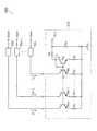
図5は、特許文献1記載のテスト回路の構成を示す図である。 FIG. 5 is a diagram showing the configuration of the test circuit described in
図5に示すように特許文献1記載のテスト回路500は、電流供給部510と、n−1個の増幅部522〜52nとを備える。 As shown in FIG. 5, the
電流供給部510は、バイポーラトランジスタにより形成されるカレントミラー回路である。電流供給部510は、外部から端子511に電圧を印加されることで、印加された電圧に応じた電流を複数の増幅部522〜52nに供給する。また、図示していないが、各増幅部の入力には受光素子が接続されている。 The
以上の構成により、特許文献1記載のテスト回路500は、外部より電圧を印加することで、複数の増幅部に電流を印加することができる。これにより、増幅部の出力であるVout端子の電圧を測定することで、増幅部の特性を測定することができる。よって、特許文献1記載のテスト回路500は、テスト時に光の照射を行うことなく、複数の増幅部を同時にテストすることができる。
しかしながら、特許文献1記載のテスト回路は、増幅部のテストを行うことはできるが、受光素子間のリーク電流の測定を行うことはできない。従来、リーク電流の測定は、増幅部のテストとは別に、各受光素子単体に対しテストパッドから電流または電圧を印加することで行われる。そのため、従来のリーク電流の測定を行うテスト回路は、各受光素子に対してテストパッドを設ける必要があり、チップサイズが大きくなるという問題がある。 However, the test circuit described in
そこで、本発明は、増幅部のテストおよび受光素子間のリーク電流のテストを行う、チップサイズの小さいテスト回路を提供することを目的とする。 SUMMARY OF THE INVENTION An object of the present invention is to provide a test circuit with a small chip size that tests an amplifier and a leak current between light receiving elements.
上記目的を達成するために、本発明に係るテスト回路は、複数の受光素子と、前記各受光素子からの光電流をそれぞれ電圧に変換する増幅手段と、前記受光素子および増幅手段に電流を供給する電流供給手段とを備え、前記電流供給手段は、前記複数の受光素子のうち行および列方向に互いに隣接しない複数の受光素子からなる第1受光素子群、および、前記第1受光素子群に含まれる受光素子に行および列方向に隣接する複数の受光素子からなる第2受光素子群に対して選択的に電流を供給する。 In order to achieve the above object, a test circuit according to the present invention includes a plurality of light receiving elements, an amplifying unit that converts a photocurrent from each of the light receiving elements into a voltage, and supplies current to the light receiving element and the amplifying unit. Current supply means, wherein the current supply means includes a first light receiving element group including a plurality of light receiving elements that are not adjacent to each other in a row and column direction, and the first light receiving element group. A current is selectively supplied to a second light receiving element group including a plurality of light receiving elements adjacent to the included light receiving elements in the row and column directions.
この構成によれば、本発明に係るテスト回路は、テスト時において、行および列方向に互いに隣接しない複数の受光素子に電流を供給し、電流を供給する受光素子に行および列方向に隣接する受光素子には電流を供給しない。これにより、隣接する受光素子間にリーク電流が生じる場合には、電流供給手段より受光素子に供給された電流は、該受光素子から該受光素子に隣接する受光素子に流れる。リーク電流により受光素子間に流れた電流は、増幅手段により増幅され、電圧として出力される。よって、増幅手段が変換し出力した電圧を測定することで、隣接する受光素子間のリーク電流を測定することができる。また、電流供給手段が電流を供給している受光素子の光電流を増幅する増幅手段が変換した出力電圧を測定することで、増幅手段の特性をテストすることができる。すなわち、本発明に係るテスト回路は、増幅手段のテストおよび受光素子間のリーク電流のテストを同時に行うことができる。また、本発明に係るテスト回路は、外部端子から電流供給手段を制御することで、複数の増幅手段の特性および受光素子間のリーク電流をテストすることができる。よって、本発明に係るテスト回路は、従来のテスト回路のように、リーク電流をテストするために各受光素子に対しテストパッドを設ける必要がなく、電流供給手段を制御するための外部端子(テストパッド)のみを設ければよい。よって、本発明に係るテスト回路は、小さいチップサイズで、増幅手段のテストおよび受光素子間のリーク電流のテストを行うことができる。 According to this configuration, the test circuit according to the present invention supplies current to a plurality of light receiving elements that are not adjacent to each other in the row and column directions during testing, and is adjacent to the light receiving elements that supply current in the row and column directions. No current is supplied to the light receiving element. As a result, when a leak current occurs between adjacent light receiving elements, the current supplied from the current supply means to the light receiving element flows from the light receiving element to the light receiving element adjacent to the light receiving element. The current flowing between the light receiving elements due to the leak current is amplified by the amplifying means and output as a voltage. Therefore, the leakage current between adjacent light receiving elements can be measured by measuring the voltage converted and output by the amplification means. Further, the characteristics of the amplifying means can be tested by measuring the output voltage converted by the amplifying means for amplifying the photocurrent of the light receiving element to which the current supplying means supplies the current. That is, the test circuit according to the present invention can simultaneously perform the test of the amplifying unit and the leak current between the light receiving elements. The test circuit according to the present invention can test the characteristics of a plurality of amplifying means and the leakage current between the light receiving elements by controlling the current supply means from an external terminal. Therefore, unlike the conventional test circuit, the test circuit according to the present invention does not need to provide a test pad for each light receiving element in order to test the leakage current, and has an external terminal for controlling the current supply means (test It is only necessary to provide a pad). Therefore, the test circuit according to the present invention can perform the test of the amplification means and the leak current between the light receiving elements with a small chip size.
また、前記電流供給手段は、前記第1受光素子群に電流を供給する第1の電流供給部と、前記第2受光素子群に電流を供給する第2の電流供給部とを備え、前記第1の電流供給部は、前記第2の電流供給部が電流を供給している間は、電流を供給せず、前記第2の電流供給部は、前記第1の電流供給部が電流を供給している間は、電流を供給しなくてもよい。 The current supply means includes a first current supply unit that supplies current to the first light receiving element group, and a second current supply unit that supplies current to the second light receiving element group. 1 current supply unit does not supply current while the second current supply unit supplies current, and the second current supply unit supplies current to the first current supply unit. During this time, it is not necessary to supply current.
この構成によれば、第1の電流供給部が電流を供給し、第2の電流供給部が電流を供給しない状態で、第2受光素子群に含まれる受光素子の光電流を変換する増幅手段の出力電圧を測定することで、受光素子間のリーク電流を測定することができる。また、同時に、第1の電流供給部が電流を供給している受光素子の光電流を変換する増幅手段の出力電圧を測定することで、該増幅手段の特性をテストすることができる。また、第2の電流供給部が電流を供給し、第1の電流供給部が電流をしない状態で、第1受光素子群に含まれる受光素子の光電流を変換する増幅手段の出力電圧を測定することで、受光素子間のリーク電流を測定することができる。また、同時に、第2の電流供給部が電流を供給している受光素子の光電流を変換する増幅手段の出力電圧を測定することで、該増幅手段の特性をテストすることができる。よって、本発明に係るテスト回路は、増幅部のテストおよび受光素子間のリーク電流のテストを同時に行うことができる。また、本発明に係るテスト回路は、外部端子から第1の電流供給部および第2の電流供給部を制御することで、複数の増幅手段の特性および受光素子間のリーク電流をテストすることができる。よって、本発明に係るテスト回路は、従来のテスト回路のように、リーク電流をテストするために各受光素子に対しテストパッドを設ける必要がなく、第1の電流供給部および第2の電流供給部を制御するための外部端子のみを設ければよい。よって、本発明に係るテスト回路は、小さいチップサイズで、増幅手段のテストおよび受光素子間のリーク電流のテストを行うことができる。 According to this configuration, the amplifying unit converts the photocurrent of the light receiving elements included in the second light receiving element group in a state where the first current supplying unit supplies current and the second current supplying unit does not supply current. , The leakage current between the light receiving elements can be measured. At the same time, the characteristics of the amplification means can be tested by measuring the output voltage of the amplification means for converting the photocurrent of the light receiving element to which the first current supply section supplies the current. Further, the output voltage of the amplifying means for converting the photocurrent of the light receiving elements included in the first light receiving element group is measured in a state where the second current supplying section supplies current and the first current supplying section does not generate current. As a result, the leakage current between the light receiving elements can be measured. At the same time, the characteristics of the amplification means can be tested by measuring the output voltage of the amplification means for converting the photocurrent of the light receiving element to which the second current supply section supplies the current. Therefore, the test circuit according to the present invention can simultaneously perform the test of the amplifier and the test of the leakage current between the light receiving elements. The test circuit according to the present invention can test the characteristics of a plurality of amplifying means and the leakage current between the light receiving elements by controlling the first current supply unit and the second current supply unit from an external terminal. it can. Therefore, unlike the conventional test circuit, the test circuit according to the present invention does not need to provide a test pad for each light receiving element in order to test the leakage current, and the first current supply unit and the second current supply. It is only necessary to provide an external terminal for controlling the unit. Therefore, the test circuit according to the present invention can perform the test of the amplification means and the leak current between the light receiving elements with a small chip size.
また、前記電流供給手段は、前記第1受光素子群に含まれる第1の受光素子に第1の電流値の電流を供給し、前記第1受光素子群に含まれる第2の受光素子に第2の電流値の電流を供給してもよい。 The current supply means supplies a current having a first current value to a first light receiving element included in the first light receiving element group, and supplies a second current to the second light receiving element included in the first light receiving element group. A current having a current value of 2 may be supplied.
この構成によれば、各受光素子および増幅手段に異なる電流値の電流を同時に供給することができる。これにより、受光素子のサイズ等が異なり、増幅手段のゲインが異なる場合であっても、増幅手段のゲインに応じた電流を供給することができる。よって、本発明に係るテスト回路は、増幅手段のゲインが異なる場合であっても、複数の増幅手段の特性を同時に、かつ、効率よく測定することができる。 According to this configuration, currents having different current values can be simultaneously supplied to the light receiving elements and the amplifying means. As a result, even when the size of the light receiving element is different and the gain of the amplification unit is different, a current corresponding to the gain of the amplification unit can be supplied. Therefore, the test circuit according to the present invention can measure the characteristics of a plurality of amplifying means simultaneously and efficiently even when the gains of the amplifying means are different.
また、前記電流供給手段は、電流を出力する電流供給部と、前記電流供給部の出力と、前記複数の受光素子および前記増幅手段との間にそれぞれ形成されるスイッチとを備えてもよい。 The current supply unit may include a current supply unit that outputs a current, an output of the current supply unit, and a switch formed between the plurality of light receiving elements and the amplification unit.
この構成によれば、スイッチのON/OFFにより、選択的に受光素子に電流を供給することができる。これにより、互いに隣接しない複数の受光素子に接続されたスイッチをONし、該受光素子に隣接する受光素子に接続されたスイッチをOFFした状態で、スイッチがOFFされている受光素子の光電流を変換する増幅手段の出力電圧を測定することで、受光素子間のリーク電流を測定することができる。また、同時に、スイッチがONされている受光素子の光電流を変換する増幅手段の出力電圧を測定することで、該増幅手段の特性をテストすることができる。よって、本発明に係るテスト回路は、増幅部のテストおよび受光素子間のリーク電流のテストを同時に行うことができる。また、本発明に係るテスト回路は、外部端子からスイッチを制御することで、複数の増幅手段の特性および受光素子間のリーク電流をテストすることができる。よって、本発明に係るテスト回路は、従来のテスト回路のように、リーク電流をテストするために各受光素子に対しテストパッドを設ける必要がなく、スイッチを制御するための外部端子のみを設ければよい。よって、本発明に係るテスト回路は、小さいチップサイズで、増幅手段のテストおよび受光素子間のリーク電流のテストを行うことができる。 According to this configuration, a current can be selectively supplied to the light receiving element by turning on / off the switch. As a result, the switch connected to a plurality of light receiving elements that are not adjacent to each other is turned ON, and the switch connected to the light receiving element adjacent to the light receiving element is turned OFF. By measuring the output voltage of the amplifying means for conversion, the leakage current between the light receiving elements can be measured. At the same time, the characteristics of the amplification means can be tested by measuring the output voltage of the amplification means for converting the photocurrent of the light receiving element whose switch is ON. Therefore, the test circuit according to the present invention can simultaneously perform the test of the amplifier and the test of the leakage current between the light receiving elements. In addition, the test circuit according to the present invention can test the characteristics of a plurality of amplifying means and the leakage current between the light receiving elements by controlling the switch from the external terminal. Therefore, unlike the conventional test circuit, the test circuit according to the present invention does not need to provide a test pad for each light receiving element in order to test the leakage current, and can only have an external terminal for controlling the switch. That's fine. Therefore, the test circuit according to the present invention can perform the test of the amplification means and the leak current between the light receiving elements with a small chip size.
また、前記テスト回路は、さらに、前記第1受光素子群に含まれる受光素子の光電流を変換する増幅手段に第1の基準電圧を供給し、前記第2受光素子群に含まれる受光素子の光電流を変換する増幅手段に第2の基準電圧を供給する電圧供給手段を備えてもよい。 The test circuit further supplies a first reference voltage to an amplifying means for converting the photocurrent of the light receiving elements included in the first light receiving element group, and the light receiving elements included in the second light receiving element group. You may provide the voltage supply means which supplies a 2nd reference voltage to the amplification means which converts a photocurrent.
この構成によれば、互いに隣接しない複数の受光素子の光電流を変換する増幅部と、該受光素子に隣接する受光素子の光電流を変換する増幅部とに異なる基準電圧を供給する。これにより、互いに隣接しない複数の受光素子と、該受光素子に隣接する受光素子とに異なる電圧を供給することができる。よって、受光素子間に電圧差が生じ、隣接する受光素子間にリーク電流が存在する場合には、該受光素子間に電流が流れ、対応する増幅手段の出力電圧が変化する。すなわち、互いに隣接しない複数の受光素子の光電流を変換する増幅部と、該受光素子に隣接する受光素子の光電流を変換する増幅部とに異なる基準電圧を供給した状態において、複数の増幅手段の出力電圧を測定することで、受光素子間のリーク電流を測定することができる。また、隣接する受光素子間に電圧差を生じさせることで、電流を供給した場合に検出できるリーク電流とは異なるモードのリーク電流を検出することができる。 According to this configuration, different reference voltages are supplied to the amplifying unit that converts the photocurrents of a plurality of light receiving elements that are not adjacent to each other and the amplifying unit that converts the photocurrents of the light receiving elements adjacent to the light receiving elements. Accordingly, different voltages can be supplied to the plurality of light receiving elements that are not adjacent to each other and the light receiving elements adjacent to the light receiving elements. Therefore, when a voltage difference occurs between the light receiving elements and a leak current exists between the adjacent light receiving elements, a current flows between the light receiving elements, and the output voltage of the corresponding amplification means changes. That is, in a state where different reference voltages are supplied to the amplifying unit that converts the photocurrents of a plurality of light receiving elements that are not adjacent to each other and the amplifying unit that converts the photocurrents of the light receiving elements adjacent to the light receiving elements, a plurality of amplifying means , The leakage current between the light receiving elements can be measured. Further, by generating a voltage difference between adjacent light receiving elements, it is possible to detect a leak current in a mode different from the leak current that can be detected when a current is supplied.
また、本発明に係るテスト方法は、複数の受光素子からの光電流をそれぞれ電圧に変換する増幅部をテストするテスト方法であって、前記複数の受光素子のうち行および列方向に互いに隣接しない複数の受光素子からなる第1受光素子群、および、前記第1受光素子群に含まれる受光素子に行および列方向に隣接する複数の受光素子からなる第2受光素子群に対して選択的に電流を供給する電流供給ステップと、前記各増幅手段が変換した電圧を測定する測定ステップと、前記第1受光素子群に含まれる受光素子の光電流を変換する増幅部が変換した電圧に基づき、該増幅部が正常に動作しているか否かを判定する第1の判定ステップと、前記第2受光素子群に含まれる受光素子の光電流を変換する増幅部が変換した電圧に基づき、前記複数の受光素子間のリーク電流を判定する第2の判定ステップとを含む。 The test method according to the present invention is a test method for testing an amplifying unit that converts photocurrents from a plurality of light receiving elements into voltages, and is not adjacent to each other in the row and column directions of the plurality of light receiving elements. Selectively with respect to a first light receiving element group including a plurality of light receiving elements and a second light receiving element group including a plurality of light receiving elements adjacent to the light receiving elements included in the first light receiving element group in a row and column direction. A current supplying step for supplying a current; a measuring step for measuring a voltage converted by each of the amplifying means; and a voltage converted by an amplifying unit for converting a photocurrent of a light receiving element included in the first light receiving element group, Based on the first determination step for determining whether or not the amplification unit is operating normally, and the voltage converted by the amplification unit that converts the photocurrent of the light receiving elements included in the second light receiving element group, And a second determination step of determining a leakage current between light-receiving elements.
これによれば、本発明に係るテスト方法は、テスト時において、互いに隣接しない複数の受光素子に電流を供給し、電流を供給する受光素子に隣接する受光素子には電流を供給しない。これにより、隣接する受光素子間にリーク電流が生じる場合には、受光素子に供給された電流は、該受光素子から該受光素子に隣接する受光素子に流れる。リーク電流により該受光素子に隣接する受光素子に流れた電流は、増幅部により増幅され、電圧として出力される。よって、増幅部が出力した電圧を測定することで、隣接する受光素子間のリーク電流を測定することができる。また、電流を供給している受光素子の光電流を増幅する増幅部の出力電圧を測定することで、増幅部の特性をテストすることができる。すなわち、本発明に係るテスト方法は、増幅部のテストおよび受光素子間のリーク電流のテストを同時に行うことができる。また、本発明に係るテスト方法は、外部端子から受光素子に供給する電流を制御することで、複数の増幅部の特性および受光素子間のリーク電流をテストすることができる。よって、本発明に係るテスト方法は、従来のように、リーク電流をテストするために各受光素子に対しテストパッドを設ける必要がなく、受光素子に供給する電流を制御するための外部端子(テストパッド)のみを設ければよい。よって、本発明に係るテスト方法を用いることで、小さいチップサイズで、増幅部のテストおよび受光素子間のリーク電流のテストを行うことができる。 According to this, the test method according to the present invention supplies current to a plurality of light receiving elements that are not adjacent to each other and does not supply current to the light receiving elements adjacent to the light receiving element that supplies current. Thereby, when a leak current occurs between adjacent light receiving elements, the current supplied to the light receiving element flows from the light receiving element to the light receiving element adjacent to the light receiving element. The current that has flowed to the light receiving element adjacent to the light receiving element due to the leak current is amplified by the amplifying unit and output as a voltage. Therefore, the leakage current between adjacent light receiving elements can be measured by measuring the voltage output from the amplifier. Further, by measuring the output voltage of the amplifying unit that amplifies the photocurrent of the light receiving element that supplies the current, the characteristics of the amplifying unit can be tested. That is, the test method according to the present invention can simultaneously perform the test of the amplifying unit and the leak current between the light receiving elements. In addition, the test method according to the present invention can test the characteristics of a plurality of amplifiers and the leakage current between the light receiving elements by controlling the current supplied to the light receiving elements from the external terminals. Therefore, the test method according to the present invention does not need to provide a test pad for each light receiving element in order to test the leakage current as in the prior art, and has an external terminal (test for controlling the current supplied to the light receiving element). It is only necessary to provide a pad). Therefore, by using the test method according to the present invention, it is possible to perform a test of the amplifier and a leak current between the light receiving elements with a small chip size.
本発明は、増幅部のテストおよび受光素子間のリーク電流のテストを行う、チップサイズの小さいテスト回路を提供することができる。 The present invention can provide a test circuit with a small chip size for testing an amplifier and a leak current between light receiving elements.
以下、本発明に係るテスト回路の実施の形態について、図面を参照しながら詳細に説明する。 Embodiments of a test circuit according to the present invention will be described below in detail with reference to the drawings.
(実施の形態1)
本実施の形態に係るテスト回路は、2つの電流供給部を用い、互いに隣接しない複数の受光素子に選択的に電流を供給する。これにより、増幅部のテストと受光素子間のリーク電流のテストとを同時に行うことができる。(Embodiment 1)
The test circuit according to the present embodiment uses two current supply units and selectively supplies current to a plurality of light receiving elements that are not adjacent to each other. Thereby, the test of the amplifier and the test of the leakage current between the light receiving elements can be performed simultaneously.
まず、実施の形態1に係るテスト回路の構成を説明する。 First, the configuration of the test circuit according to the first embodiment will be described.
図1は、実施の形態1に係るテスト回路の構成を示す図である。 FIG. 1 is a diagram illustrating a configuration of a test circuit according to the first embodiment.
図1に示すテスト回路100は、受光素子101〜104と、増幅部111〜114と、第1の電流供給部121と、第2の電流供給部122とを備える。テスト回路100は、複数の増幅部111〜114の特性のテスト行う。さらに、テスト回路100は、受光素子101〜104間のリーク電流のテストを行う。 The
受光素子101〜104は、照射された光を電流に変換するフォトダイオード等である。また、受光素子101〜104は、格子状に配置される。 The
増幅部111〜114は、例えば、差動増幅回路である。増幅部111〜114には、それぞれ基準電圧Vref1〜Vref4が入力され、それぞれ抵抗R01〜R04を介して負帰還を形成する。増幅部111〜114は、それぞれ受光素子101〜104からの光電流を電圧に変換する。増幅部111は、受光素子101からの光電流を変換および増幅し、電圧Vout1として出力する。増幅部112は、受光素子102からの光電流を変換および増幅し、電圧Vout2として出力する。増幅部113は、受光素子103からの光電流を変換および増幅し、電圧Vout3として出力する。増幅部114は、受光素子104からの光電流を変換および増幅し、電圧Vout4として出力する。 The
第1の電流供給部121は、行および列方向に互いに隣接しない複数の受光素子に電流を供給する。具体的には、第1の電流供給部121は、受光素子101および受光素子101の光電流を変換する増幅部111と、受光素子101と隣接しない受光素子103および受光素子103の光電流を変換する増幅部113とに電流を供給する。第1の電流供給部121は、抵抗R10〜R14およびNPNバイポーラトランジスタTr10〜Tr12により構成されるカレントミラー回路である。第1の電流供給部121は、外部(半導体テスタ等)からVin1端子に印加された電圧に応じた電流を供給する。 The first
抵抗R10は、Vin1端子とGNDとの間に接続される。トランジスタTr10のコレクタおよびベースは抵抗R11を介してVin1端子に接続され、エミッタは抵抗R12を介してGNDに接続される。トランジスタTr11のベースはトランジスタTr10のコレクタおよびベースと接続され、コレクタは受光素子101および増幅部111の入力と接続され、エミッタは抵抗R13を介してGNDと接続される。トランジスタTr12のベースはトランジスタTr10のコレクタおよびベースと接続され、コレクタは受光素子103および増幅部113の入力と接続され、エミッタは抵抗R14を介してGNDと接続される。例えば、抵抗R12、R13およびR14の抵抗値は等しく、トランジスタTr10、Tr11およびTr12のサイズは等しい。これにより、Vin1端子に印加された電圧に応じた電流値が抵抗R11、トランジスタTr10および抵抗R12に流れ、該電流値と等しい電流がトランジスタTr11およびTr12に流れ、該電流が増幅部111および113に供給される。 The resistor R10 is connected between the Vin1 terminal and GND. The collector and base of the transistor Tr10 are connected to the Vin1 terminal via the resistor R11, and the emitter is connected to GND via the resistor R12. The base of the transistor Tr11 is connected to the collector and base of the transistor Tr10, the collector is connected to the input of the
第2の電流供給部122は、第1の電流供給部121が電流を供給する受光素子に行および列方向に隣接する受光素子に電流を供給する。具体的には、第2の電流供給部122は、受光素子102および受光素子102の光電流を変換する増幅部112と、受光素子102と隣接しない受光素子104および受光素子104の光電流を変換する増幅部114に電流を供給する。第2の電流供給部122は、抵抗R20〜R24およびNPNバイポーラトランジスタTr20〜Tr22により構成されるカレントミラー回路である。第2の電流供給部122は、Vin2端子に印加された電圧に応じた電流を供給する。なお、第2の電流供給部122の詳細な構成は、第1の電流供給部121と同様であり、詳細な説明は省略する。 The second
次に、本実施の形態に係るテスト回路100の動作を説明する。 Next, the operation of the
まず、Vin1端子に外部より所定の電圧の信号が印加され、Vin2端子はGNDレベルに接続される。ここで、所定の電圧の信号とは、テスト内容に応じた信号であり、例えば、所定の周波数の正弦波形の信号またはDC電圧等である。また、テスト時には、受光素子101〜104に光照射は行われず、受光素子101〜104は光電流を生成しない。 First, a signal having a predetermined voltage is applied to the Vin1 terminal from the outside, and the Vin2 terminal is connected to the GND level. Here, the signal of a predetermined voltage is a signal according to the test content, for example, a signal of a sine waveform of a predetermined frequency or a DC voltage. In the test, the
第1の電流供給部121は、Vin1端子に印加された電圧に応じた電流を増幅部111および113に供給する。増幅部111および113は、該電流を増幅および電圧に変換し、Vout1端子およびVout3端子に出力する。よって、Vin1端子に印加された電圧に対するVout1端子およびVout3端子の電圧を測定することで、増幅部111および113の特性(電流電圧特性および周波数特性等)を測定することができる。すなわち、増幅部111および113が変換した電圧に基づき、増幅部111および113が正常に動作しているか否かを判定することができる。The first
一方、第2の電流供給部122は、Vin2端子がGNDレベルに接続されているので、受光素子102、受光素子104、増幅部112および増幅部114に電流を供給しない。このとき、受光素子間でリーク電流が発生していると、第1の電流供給部121から供給された電流が、受光素子101または103から、受光素子102または104に流れる。これにより、増幅部112または114は、受光素子102または104に流れ込んだ電流を増幅し、電圧に変換する。よって、Vout2端子およびVout4端子の電圧を測定することで、受光素子間に発生するリーク電流を測定することができる。 On the other hand, since the Vin2 terminal is connected to the GND level, the second
次に、Vin2端子に外部より所定の電圧が印加され、Vin1端子はGNDレベルに接続される。 Next, a predetermined voltage is applied to the Vin2 terminal from the outside, and the Vin1 terminal is connected to the GND level.
第2の電流供給部122は、Vin2端子に印加された電圧に応じた電流を増幅部112および114に供給する。増幅部112および114は、該電流を増幅および電圧に変換し、Vout2端子およびVout4端子に出力する。よって、Vin2端子に印加された電圧に対するVout2端子およびVout4端子の電圧を測定することで、増幅部112および114の特性を測定することができる。すなわち、増幅部112および114が変換した電圧に基づき、増幅部112および114が正常に動作しているか否かを判定することができる。The second
一方、第1の電流供給部121は、Vin1端子がGNDレベルに接続されているので、受光素子101、受光素子101、増幅部111および増幅部113に電流を供給しない。このとき、受光素子間でリーク電流が発生していると、第2の電流供給部122から供給された電流が、受光素子102または104から、受光素子101または103に流れる。これにより、増幅部111または113は、受光素子101または103に流れ込んだ電流を増幅し、電圧に変換する。よって、Vout1端子およびVout3端子の電圧を測定することで、受光素子間に発生するリーク電流を測定することができる。また、この時測定される受光素子間のリーク電流は、Vin1端子に電圧が印加され、Vin2端子はGNDレベルに接続された状態で測定できる受光素子間のリーク電流とは逆方向のリーク電流である。 On the other hand, since the Vin1 terminal is connected to the GND level, the first
以上の動作により、増幅部111〜114の特性の測定、および、受光素子101〜104間のリーク電流を測定することができる。従来のテスト回路では、増幅部111〜114の特性の測定と、受光素子101〜104間のリーク電流の測定は、個別に行われていた。これに対し、本実施の形態に係るテスト回路は、増幅部111〜114の特性の測定と、受光素子101〜104間のリーク電流を測定とを同じ回路で、同時に測定することができる。よって、本実施の形態に係るテスト回路は、増幅部111〜114のテストおよび受光素子101〜104間のリーク電流のテストを短時間で効率よく行うことができる。 With the above operation, the characteristics of the
また、本実施の形態に係るテスト回路100は、外部からVin1端子およびVin2端子の電圧を制御することで、増幅部111〜114の特性の測定、および、受光素子101〜104間のリーク電流を測定することができる。すなわち、本実施の形態に係るテスト回路100は、Vin1端子およびVin2端子に電圧を印加するための2つのテストパッドのみを設ければよい。一方、従来のリーク電流のテストを行うテスト回路は、各受光素子101〜104に対しテストパッドを設ける必要があり、受光素子が4つの場合には4つのテストパッドが必要である。よって、本実施の形態に係るテスト回路100は、従来のテスト回路と比べ、テストパッドの数を減らすことができる。すなわち、チップサイズを小さくすることができる。 In addition, the
なお、上記説明において、受光素子および増幅部の数が4の場合について説明したが、これに限定されるものではない。受光素子および増幅部は複数であればよく、受光素子および増幅部の数が3以下または5以上であっても同様の効果を得ることができる。また、受光素子および増幅部の数が多い場合には、従来のリーク電流のテストを行うテスト回路と比べ、より多くのテストパッドを削減することができる。 In the above description, the case where the number of light receiving elements and amplifying units is four has been described. However, the present invention is not limited to this. There may be a plurality of light receiving elements and amplifying units, and the same effect can be obtained even if the number of light receiving elements and amplifying units is 3 or less or 5 or more. Further, when the number of light receiving elements and amplifying units is large, it is possible to reduce more test pads as compared with a conventional test circuit that performs a leakage current test.
また、上記説明において、第1の電流供給部111のカレントミラー回路を構成する抵抗R12、R13およびR14の抵抗値は等しく、トランジスタTr10、Tr11およびTr12のサイズは等しいとしたが、これに限定されるものでなく、任意の抵抗値またはトランジスタサイズであってよい。例えば、トランジスタTr10に流れる電流を整数倍した電流がTr11およびTr12に流れるようにトランジスタTr10、Tr11およびTr12のサイズを設定してもよい。 In the above description, the resistance values of the resistors R12, R13, and R14 that constitute the current mirror circuit of the first
また、上記説明において、第1の電流増幅部111および第2の電流増幅部112は、NPNバイポーラトランジスタで構成されるとしたが、PNPバイポーラトランジスタで構成してもよい。さらに、第1の電流増幅部111および第2の電流増幅部112を電界効果トランジスタで構成してもよい。 In the above description, the first
また、上記説明において、第1の電流増幅部111および第2の電流増幅部112は、外部からVin1端子またはVin2端子に電圧を印加されることで動作するとしたが、外部より電流を印加されることで動作してもよい。例えば、抵抗R10およびR11(抵抗R20およびR21)を設けず、トランジスタTr10のコレクタおよびベースに電流を印加する方式としてもよい。 In the above description, the first
また、上記説明において、Vin1端子およびVin2端子に印加される電圧は、外部から供給されるとしたが、これに限定されるものではない。例えば、テスト回路100と同じ半導体基板上に形成された内部回路が、外部からの信号に基づいてVin1端子およびVin2端子に電圧を印加してもよい。 In the above description, the voltages applied to the Vin1 terminal and the Vin2 terminal are supplied from the outside. However, the present invention is not limited to this. For example, an internal circuit formed on the same semiconductor substrate as the
また、上記説明において、電流供給部の数は2としたが、各電流供給部が互いに隣接しない受光素子に選択的に電流を供給できる構成であれば3以上であってもよい。 In the above description, the number of current supply units is 2. However, the number of current supply units may be 3 or more as long as each current supply unit can selectively supply current to light receiving elements that are not adjacent to each other.
(実施の形態2)
実施の形態1では、テスト時において、各受光素子に等しい電流値の電流を供給するテスト回路100について説明したが、実施の形態2では、各受光素子に異なる電流を供給するテスト回路200について説明する。(Embodiment 2)
In the first embodiment, the
例えば、CDまたはDVDからの光信号を電気信号変換するための光ピックアップ用PDICにおいては、設計上、各受光素子のサイズを同一にしない場合、または、サイズが同一であっても各受光素子が受光する光の光量が異なる場合がある。この場合、各受光素子が受光した時に生成する光電流の電流値も異なる。また、各増幅部は、対応する受光素子の光電流の電流値に応じゲインが設定される。ゲインが異なる増幅部をテストする場合、テスト時に要求される増幅部に入力される電流値の範囲は異なる。よって、電流供給部が、選択した増幅部の全てに同じ電流値の電流を供給しテストを行った場合、各増幅部のゲインが異なると効率よくテストを行うことができない。 For example, in an optical pickup PDIC for converting an optical signal from a CD or DVD into an electrical signal, if the size of each light receiving element is not the same by design, or each light receiving element is the same size The amount of light received may be different. In this case, the current value of the photocurrent generated when each light receiving element receives light is also different. Further, each amplifying unit has a gain set according to the current value of the photocurrent of the corresponding light receiving element. When testing amplifying units with different gains, the range of current values input to the amplifying unit required during the test is different. Therefore, when the current supply unit supplies a current having the same current value to all of the selected amplification units and performs a test, the test cannot be performed efficiently if the gains of the amplification units are different.
図2は、本発明の実施の形態2に係るテスト回路の構成を示す図である。なお、図1と同様の要素には同一の符号を付しており、詳細な説明は省略する。 FIG. 2 is a diagram showing a configuration of a test circuit according to the second embodiment of the present invention. Elements similar to those in FIG. 1 are denoted by the same reference numerals, and detailed description thereof is omitted.
図2に示すテスト回路200は、受光素子101、102、203および204と、増幅部111、112、213および214と、第1の電流供給部131と、第2の電流供給部132とを備える。テスト回路200は、複数の増幅部111、112、213および214の特性のテスト行う。さらに、テスト回路200は、受光素子101、102、203および204間のリーク電流のテストを行う。 The
受光素子203および204は、受光素子101および102の2倍のサイズであり、2倍の電流値の光電流を生成する。 The
増幅部213および214は、増幅部111および112の半分のゲインである。 The
第1の電流供給部131は、実施の形態1における第1の電流供給部121に加え、トランジスタTr13と、抵抗R15とを備える。トランジスタTr13のベースはトランジスタTr10のコレクタおよびベースと接続され、コレクタは受光素子203および増幅部213の入力と接続され、エミッタは抵抗R15を介してGNDと接続される。ここで、トランジスタTr10〜Tr13のサイズは同じであり、抵抗R12〜R15の抵抗値は同じとする。以上の構成により、第1の電流供給部131において、Vin1端子に印加された電圧に応じた電流がトランジスタTr10に流れる。トランジスタTr10に流れる電流値と同じ電流値の電流がトランジスタTr11、Tr12およびTr13に流れる。すなわち、受光素子101および増幅部111に供給される電流の電流値の2倍の電流値の電流が受光素子203および増幅部213に供給される。 The first
第2の電流供給部132は、実施の形態1における第2の電流供給部122に加え、トランジスタTr23と、抵抗R25とを備える。トランジスタTr23のベースはトランジスタTr20のコレクタおよびベースと接続され、コレクタは受光素子204および増幅部214の入力と接続され、エミッタは抵抗R25を介してGNDと接続される。ここで、トランジスタTr20〜Tr23のサイズは同じであり、抵抗R22〜R25の抵抗値は同じとする。以上の構成により、第2の電流供給部132において、Vin2端子に印加された電圧に応じた電流がトランジスタTr20に流れる。トランジスタTr20に流れる電流値と同じ電流値の電流がトランジスタTr21、Tr22およびTr23に流れる。すなわち、受光素子102および増幅部112に供給される電流の電流値の2倍の電流値の電流が受光素子204および増幅部214に供給される。 The second
以上の構成により、本実施の形態に係るテスト回路200は、Vin1端子に外部より所定の電圧を印加し、Vin2端子をGNDレベルに接続した状態において、増幅部213に増幅部111に供給される電流の電流値の2倍の電流値が供給される。すなわち、テスト時において、第1の電流供給部131は、受光素子101および203に光が照射された時に発生する光電流の電流値の比率と同じ比率の電流値の電流を、増幅部111および213に供給する。これにより、Vin1端子に印加された電圧に対するVout1端子およびVout3端子の電圧を測定することで、増幅部111と、増幅部111の半分のゲインの増幅部213との特性を、効率よく同時に測定することができる。また、実施の形態1と同様に、Vout2端子およびVout4端子の電圧を測定することで、受光素子間のリーク電流を測定することができる。 With the above configuration, the
また、Vin2端子に外部より所定の電圧を印加し、Vin1端子をGNDレベルに接続した状態において、増幅部214に増幅部112に供給される電流の電流値の2倍の電流値が供給される。これにより、Vin2端子に印加された電圧に対するVout2端子およびVout4端子の電圧を測定することで、増幅部112と、増幅部112の半分のゲインの増幅部214との特性を、効率よく同時に測定することができる。また、実施の形態1と同様に、Vout1端子およびVout3端子の電圧を測定することで、受光素子間のリーク電流を測定することができる。また、実施の形態1と同様に、チップサイズを小さくすることができる。 In addition, when a predetermined voltage is applied to the Vin2 terminal from the outside and the Vin1 terminal is connected to the GND level, the
なお、上記説明において、受光素子203および204の光電流の電流値が受光素子1101および102の光電流の電流値の2倍の場合について説明したが、これに限定されるものではない。各受光素子の光電流の電流値の比率または増幅部のゲインの比率は任意でよく、各受光素子の光電流の電流値の比率または増幅部のゲインの比率に応じ、電流供給部131または132が各受光素子および増幅部に供給する電流の電流値の比率を変更すればよい。 In the above description, the case where the current value of the photocurrent of the
(実施の形態3)
本発明の実施の形態3に係るテスト回路は、1つの電流供給部から供給される電流をスイッチにより互いに隣接しない受光素子に選択的に供給する。これにより、増幅部のテストと受光素子間のリーク電流のテストとを同時に行うことができる。(Embodiment 3)
The test circuit according to Embodiment 3 of the present invention selectively supplies current supplied from one current supply unit to light receiving elements that are not adjacent to each other by a switch. Thereby, the test of the amplifier and the test of the leakage current between the light receiving elements can be performed simultaneously.
まず、実施の形態3に係るテスト回路の構成を説明する。 First, the configuration of the test circuit according to the third embodiment will be described.
図3は、本発明の実施の形態3に係るテスト回路の構成を示す図である。なお、図1と同様の要素には同一の符号を付しており、詳細な説明は省略する。 FIG. 3 is a diagram showing a configuration of a test circuit according to the third embodiment of the present invention. Elements similar to those in FIG. 1 are denoted by the same reference numerals, and detailed description thereof is omitted.
図3に示すテスト回路300は、受光素子101〜104と、増幅部111〜114と、電流供給部141と、スイッチ151〜154とを備える。テスト回路300は、複数の増幅部111〜114の特性のテスト行う。さらに、テスト回路300は、受光素子101〜104間のリーク電流のテストを行う。 The
電流供給部141は、NPNバイポーラトランジスタTr40〜Tr44と、抵抗R40〜R46とを備えるカレントミラー回路である。電流供給部141は、Vin端子に印加された電圧に応じた電流を出力する。 The
抵抗R40は、Vin端子とGNDとの間に接続される。トランジスタTr40のコレクタおよびベースは抵抗R41を介してVin端子に接続され、エミッタは抵抗R42を介してGNDに接続される。トランジスタTr41のベースはトランジスタTr40のコレクタおよびベースと接続され、コレクタはスイッチ151と接続され、エミッタは抵抗R43を介してGNDと接続される。トランジスタTr42のベースはトランジスタTr40のコレクタおよびベースと接続され、コレクタはスイッチ152と接続され、エミッタは抵抗R44を介してGNDと接続される。トランジスタTr43のベースはトランジスタTr40のコレクタおよびベースと接続され、コレクタはスイッチ153と接続され、エミッタは抵抗R45を介してGNDと接続される。トランジスタTr44のベースはトランジスタTr40のコレクタおよびベースと接続され、コレクタはスイッチ154と接続され、エミッタは抵抗R46を介してGNDと接続される。例えば、抵抗R42〜R46の抵抗値は等しく、トランジスタTr40〜Tr44のサイズは等しい。これにより、Vin端子に印加された電圧に応じた電流値がトランジスタTr40に流れ、該電流値と等しい電流がTr41〜Tr44に流れる。 The resistor R40 is connected between the Vin terminal and GND. The collector and base of the transistor Tr40 are connected to the Vin terminal via the resistor R41, and the emitter is connected to GND via the resistor R42. The base of the transistor Tr41 is connected to the collector and base of the transistor Tr40, the collector is connected to the
スイッチ151〜154は、電流供給部141と、受光素子101〜104および増幅部111〜114の入力との間にそれぞれ形成される。スイッチ151〜154は、例えば、トランジスタで形成されるアナログスイッチ等である。例えば、スイッチ151〜154のON/OFFは、テスト時に外部から印加される信号により制御される。スイッチ151は、トランジスタTr41と受光素子101および増幅部111の入力との間に形成される。スイッチ152は、トランジスタTr42と受光素子102および増幅部112の入力との間に形成される。スイッチ153は、トランジスタTr43と受光素子103および増幅部113の入力との間に形成される。スイッチ154は、トランジスタTr44と受光素子104および増幅部114の入力との間に形成される。 The
次に、実施の形態3に係るテスト回路300の動作を説明する。 Next, the operation of the
まず、スイッチ151および153をONし、スイッチ152および154をOFFする。また、Vin端子には所定の電圧が印加される。 First, the
スイッチ151および153がONしているので、電流供給部141は、Vin端子に印加された電圧に応じた電流を増幅部111および113に供給する。増幅部111および113は、該電流を増幅および電圧に変換し、Vout1端子およびVout3端子に出力する。よって、Vin端子に印加された電圧に対するVout1端子およびVout3端子の電圧を測定することで、増幅部111および113の特性を測定することができる。Since the
一方、スイッチ152およびスイッチ154がOFFしているので、受光素子102、受光素子104、増幅部112および増幅部114には電流が供給されていない。このとき、受光素子間でリーク電流が発生していると、電流供給部141から供給された電流が、受光素子101または103から、受光素子102または104に流れる。これにより、増幅部112または114は、受光素子102または104に流れ込んだ電流を増幅し、電圧に変換する。よって、Vout2端子およびVout4端子の電圧を測定することで、受光素子間に発生するリーク電流を測定することができる。 On the other hand, since the
次に、スイッチ152および154をONし、スイッチ151および153をOFFする。また、Vin端子には所定の電圧が印加される。 Next, the
スイッチ152および154がONしているので、電流供給部141は、Vin端子に印加された電圧に応じた電流を増幅部112および114に供給する。増幅部112および114は、該電流を増幅および電圧に変換し、Vout2端子およびVout4端子に出力する。よって、Vin端子に印加された電圧に対するVout2端子およびVout4端子の電圧を測定することで、増幅部112および114の特性を測定することができる。Since the
一方、スイッチ151およびスイッチ153がOFFしているので、受光素子101、受光素子103、増幅部111および増幅部113には電流が供給されていない。このとき、受光素子間でリーク電流が発生していると、電流供給部141から供給された電流が、受光素子102または104から、受光素子101または103に流れる。これにより、増幅部111または113は、受光素子101または103に流れ込んだ電流を増幅し、電圧に変換する。よって、Vout1端子およびVout3端子の電圧を測定することで、受光素子間に発生するリーク電流を測定することができる。 On the other hand, since the
以上の動作により、増幅部111〜114の特性の測定、および、受光素子101〜104間のリーク電流を測定することができる。従来のテスト回路では、増幅部111〜114の特性の測定と、受光素子101〜104間のリーク電流の測定は、個別に行われていた。これに対し、本実施の形態に係るテスト回路は、増幅部111〜114の特性の測定と、受光素子101〜104間のリーク電流を測定とを同じ回路で、同時に測定することができる。よって、本実施の形態に係るテスト回路は、増幅部111〜114のテストおよび受光素子101〜104間のリーク電流のテストを短時間で効率よく行うことができる。 With the above operation, the characteristics of the
また、実施の形態3に係るテスト回路300は、外部からVin端子およびスイッチ151〜154を制御することで、増幅部111〜114の特性の測定、および、受光素子101〜104間のリーク電流を測定することができる。例えば、実施の形態3に係るテスト回路300は、Vin端子に電圧を印加するためのテストパッド、および、スイッチ151〜154を選択的にON/OFFさせる2ビットの制御信号(スイッチ151および153の制御信号と、スイッチ152および154の制御信号)を印加するための2つのテストパッドのみを設ければよい。なお、スイッチ151〜154を制御する制御信号は1ビットであり、制御信号のH/Lにより、スイッチ151および153と、スイッチ152および154の一方がON、他方がOFFしてもよい。一方、従来のリーク電流のテストを行うテスト回路は、各受光素子101〜104に対しテストパッドを設ける必要があり、受光素子が4つの場合には4つのテストパッドが必要である。よって、実施の形態3に係るテスト回路300は、従来のテスト回路と比べ、テストパッドの数を減らすことができる。すなわち、チップサイズを小さくすることができる。 Further, the
また、実施の形態3に係るテスト回路300は、出荷後の通常動作時(テスト時以外)においてスイッチ151〜154はOFFされる。これにより、通常動作時には、受光素子および増幅部に対する電流供給部の寄生負荷の影響を低減することができる。 In the
なお、上記説明において、電流供給部141は4つの電流出力を有し、スイッチとして4つのSPSTスイッチを用いた構成としたがこれに限定されるものではない。例えば、電流供給部141の電流出力を2とし(例えば、電流供給部141は、トランジスタTr43、Tr44、抵抗R45およびR46を備えない。)、スイッチとして2つのSPDTスイッチを用い、選択的に受光素子および増幅部に電流を供給してもよい。 In the above description, the
(実施の形態4)
上述した実施の形態1では、電流供給部が供給した電流の回り込み(例えば、受光素子101に供給した電流が、受光素子101と受光素子102との間のリーク電流により、受光素子102側に回り込むこと)を検出することで、各受光素子間のリーク電流を測定した。実施の形態4では、増幅部の基準電圧を選択的に制御することで、受光素子間に電圧差を生じさせ、電流の回り込みでは検出できないモードのリーク電流を検出するテスト回路について説明する。(Embodiment 4)
In the first embodiment described above, the current supplied by the current supply unit wraps around (for example, the current supplied to the
まず、本発明の実施の形態4に係るテスト回路の構成を説明する。 First, the configuration of the test circuit according to the fourth embodiment of the present invention will be described.
図4は、本発明の実施の形態4に係るテスト回路の構成を示す図である。なお、図1と同様の要素には同一の符号を付しており、詳細な説明は省略する。 FIG. 4 is a diagram showing a configuration of a test circuit according to the fourth embodiment of the present invention. Elements similar to those in FIG. 1 are denoted by the same reference numerals, and detailed description thereof is omitted.
図4に示すテスト回路400は、図1に示す実施の形態1に係るテスト回路100の構成に加え、電圧供給部160を備える。 A
電圧供給部160は、増幅部111〜114に基準電圧を供給する。また、電圧供給部160は、テスト時において、増幅部111および113と、増幅部112および114とに異なる基準電圧を供給する。すなわち、電圧供給部160は、複数の受光素子のうち、互いに隣接しない複数の受光素子の光電流を変換する増幅部と、該受光素子と隣接する受光素子の光電流を変換する増幅部とに、異なる基準電圧を供給する。 The
次に、実施の形態4に係るテスト回路400の動作を説明する。 Next, the operation of the
まず、実施の形態1と同様に、Vin1端子に外部より所定の電圧を印加し、Vin2端子をGNDレベルに接続した状態で、Vout1〜Vout4端子の電圧を測定することで、増幅部111および113の特性、および、受光素子間のリーク電流を測定する。また、Vin2端子に外部より所定の電圧が印加し、Vin1端子をGNDレベルに接続した状態で、Vout1〜Vout4端子の電圧を測定することで、増幅部112および114の特性、および、受光素子間のリーク電流を測定する。なお、上記テスト動作中は、電圧供給部160は、増幅部111〜114に同一の基準電圧を供給する。例えば、電圧供給部160が供給する基準電圧は、通常動作に用いられる基準電圧に基づく電圧(例えば、仕様に基づく増幅部111〜114の特性に対するワースト条件となる基準電圧等)である。 First, as in the first embodiment, a predetermined voltage is applied to the Vin1 terminal from the outside, and the voltages at the Vout1 to Vout4 terminals are measured in a state where the Vin2 terminal is connected to the GND level. And the leakage current between the light receiving elements are measured. In addition, by measuring a voltage at the Vout1 to Vout4 terminals while a predetermined voltage is applied to the Vin2 terminal from the outside and the Vin1 terminal is connected to the GND level, characteristics of the amplifying
次に、Vin1端子およびVin2端子をGNDに接続した状態で、電圧供給部160は、増幅部111および113と、増幅部112および114とに異なる基準電圧を供給する。例えば、電圧供給部160は、増幅部111および113に基準電圧として2Vを供給し、増幅部112および114に基準電圧として1Vを供給する。この時、イマジナリーショートにより増幅部111および113の差動入力の他端の電圧は2Vとなり、増幅部112および114の差動入力の他端の電圧は1Vとなる。すなわち、受光素子101および103に2Vが供給され、受光素子102および104に1Vが供給される。これにより、隣接する受光素子間において電圧差(1V)が生じ、電圧差により隣接する受光素子間にリーク電流が発生すると、リーク電流が発生している受光素子に対応する増幅部の出力電圧が変動する。例えば、受光素子101と受光素子102との間にリーク電流が発生している場合には、Vout1端子およびVout2端子の電圧が変動する。よって、増幅部111および113と、増幅部112および114とに異なる基準電圧を供給している状態において、Vout1〜Vout4端子の電圧を測定することで受光素子間のリーク電流を測定することができる。また、隣接する受光素子間に電圧差を発生させることで、隣接する受光素子間での電流の回り込みにより検出するリーク電流とは異なるモードのリーク電流を検出することができる。 Next, the
以上より、本発明の実施の形態4に係るテスト回路400は、実施の形態1に係るテスト回路100の効果に加え、受光素子間の多種のモードのリーク電流をテストすることができる。 As described above, the
なお、上記説明において、隣接しない受光素子に選択的に電流を供給するテストを行った後、異なる基準電圧を印加するテストを行うとしたが、電流の回り込みによる受光素子間のテストを行わない場合には、全ての増幅部111〜114に一括して電流を供給しテストを行った後、異なる基準電圧を印加するテストを行うことで、複数の増幅部のテストと、受光素子間の電圧差で検知できるリーク電流のテストを行うことができる。 In the above description, after a test for selectively supplying current to light receiving elements that are not adjacent to each other, a test for applying a different reference voltage is performed. However, a test between light receiving elements due to current wraparound is not performed. In this case, a test is performed by supplying current to all the amplifying
本発明は、テスト回路に適用でき、特にCDプレーヤまたはDVDプレーヤ等の光ドライブに用いられる光ピックアップ用PDICに内蔵されるテスト回路に適用できる。The present invention is applicable to the test circuit, particularly applicable to a test circuit incorporated in the optical pickup PDIC used for an optical drive such as CD playya or DVD player.
100、200、300、400、500 テスト回路
101〜104、203、204 受光素子
111〜114、213、214、522〜52n 増幅部
121、131 第1の電流供給部
122、132 第2の電流供給部
141、510 電流供給部
151〜154 スイッチ
160 電圧供給部
511 端子100, 200, 300, 400, 500 Test circuit 101-104, 203, 204 Light receiving element 111-114, 213, 214, 522-
Claims (6)
Translated fromJapanese前記各受光素子からの光電流をそれぞれ電圧に変換する増幅手段と、
外部から電圧が入力されるテストパッドと、
前記受光素子および増幅手段に、前記テストパッドに入力された電圧に応じた電流を供給する電流供給手段とを備え、
前記電流供給手段は、前記複数の受光素子のうち行および列方向に互いに隣接しない複数の受光素子からなる第1受光素子群、および、前記第1受光素子群に含まれる受光素子に行および列方向に隣接する複数の受光素子からなる第2受光素子群に対して選択的に電流を供給することにより、前記第1受光素子群及び前記第2受光素子群のうち、電流が供給された受光素子群に含まれる受光素子の光電流を変換する増幅手段に、当該増幅手段が正常に動作しているか否かを判定するための電圧を出力させ、前記第1受光素子群及び前記第2受光素子群のうち、電流が供給されていない受光素子群に含まれる受光素子の光電流を変換する増幅手段に、前記複数の受光素子間のリーク電流を判定するための電圧を出力させる
ことを特徴とする受光増幅回路のテスト回路。A plurality of light receiving elements;
Amplifying means for converting the photocurrent from each of the light receiving elements into a voltage;
A test pad to which voltage is input from the outside,
A current supply means for supplyinga currentcorresponding to a voltage input to the test pad to the light receiving element and the amplification means;
The current supply means includes a first light receiving element group including a plurality of light receiving elements that are not adjacent to each other in a row and column direction, and a light receiving element included in the first light receiving element group. By selectively supplying a current to a second light receiving element group composed of a plurality of light receiving elements adjacent to each other in the direction, light reception towhich a current is supplied from the first light receiving element group and the second light receiving element group is provided. Amplifying means for converting the photocurrent of the light receiving elements included in the element group outputs a voltage for determining whether or not the amplifying means is operating normally, and the first light receiving element group and the second light receiving element are output. Amplifying means for converting a photocurrent of a light receiving element included in a light receiving element group to which no current is supplied out of the element group outputs a voltage for determining a leakage current between the plurality of light receiving elements.light to Test circuitof width circuit.
前記第1受光素子群に電流を供給する第1の電流供給部と、
前記第2受光素子群に電流を供給する第2の電流供給部とを備え、
前記第1の電流供給部は、前記第2の電流供給部が電流を供給している間は、電流を供給せず、
前記第2の電流供給部は、前記第1の電流供給部が電流を供給している間は、電流を供給しない
ことを特徴とする請求項1記載の受光増幅回路のテスト回路。The current supply means includes
A first current supply unit for supplying current to the first light receiving element group;
A second current supply unit for supplying current to the second light receiving element group,
The first current supply unit does not supply current while the second current supply unit supplies current,
2.The test circuit for alight receiving amplification circuit according to claim 1, wherein the second current supply unit does not supply a current while the first current supply unit supplies a current. 3.
ことを特徴とする請求項1または2記載の受光増幅回路のテスト回路。The current supply means supplies a current having a first current value to a first light receiving element included in the first light receiving element group, and supplies a second current to the second light receiving element included in the first light receiving element group. Thelight receiving amplifier circuit test circuit according to claim 1, wherein a current having a current value is supplied.
電流を出力する電流供給部と、
前記電流供給部の出力と、前記複数の受光素子および前記増幅手段との間にそれぞれ形成されるスイッチとを備える
ことを特徴とする請求項1記載の受光増幅回路のテスト回路。The current supply means includes
A current supply unit for outputting current;
The test circuit for alight receiving and amplifying circuit according to claim 1, further comprising a switch formed between an output of the current supply unit and the plurality of light receiving elements and the amplifying unit.
前記第1受光素子群に含まれる受光素子の光電流を変換する増幅手段に第1の基準電圧を供給し、前記第2受光素子群に含まれる受光素子の光電流を変換する増幅手段に第2の基準電圧を供給する電圧供給手段を備える
ことを特徴とする請求項1記載の受光増幅回路のテスト回路。The test circuit further includes:
A first reference voltage is supplied to the amplifying means for converting the photocurrent of the light receiving elements included in the first light receiving element group, and the amplifying means for converting the photocurrent of the light receiving elements included in the second light receiving element group. 2. A test circuit for alight receiving amplification circuit according to claim 1, further comprising voltage supply means for supplying two reference voltages.
前記複数の受光素子のうち行および列方向に互いに隣接しない複数の受光素子からなる第1受光素子群、および、前記第1受光素子群に含まれる受光素子に行および列方向に隣接する複数の受光素子からなる第2受光素子群に対して選択的に、テストパッドに入力された電圧に応じた電流を供給する電流供給ステップと、
前記テストパッドに入力された電圧に対する前記各増幅手段が変換した電圧を測定する測定ステップと、
前記第1受光素子群及び前記第2受光素子群のうち、電流が供給された受光素子群に含まれる受光素子の光電流を変換する増幅部が変換した電圧に基づき、該増幅部が正常に動作しているか否かを判定する第1の判定ステップと、
前記第1受光素子群及び前記第2受光素子群のうち、電流が供給されていない受光素子群に含まれる受光素子の光電流を変換する増幅部が変換した電圧に基づき、前記複数の受光素子間のリーク電流を判定する第2の判定ステップとを含む
ことを特徴とする受光増幅回路のテスト方法。A method for testing alight receiving amplification circuit that tests an amplification unit that converts photocurrents from a plurality of light receiving elements into voltages, respectively.
Of the plurality of light receiving elements, a first light receiving element group including a plurality of light receiving elements that are not adjacent to each other in the row and column directions, and a plurality of light receiving elements included in the first light receiving element group that are adjacent to each other in the row and column directions. A current supply step for selectively supplyinga currentcorresponding to a voltage input to the test pad to the second light receiving element group including the light receiving elements;
A measuring step of measuring a voltage converted by each of the amplifying means withrespect to a voltage input to the test pad ;
Based on the voltage converted by the amplifier that converts the photocurrent of the light receiving element included in the lightreceiving element group to which the current is supplied out of the first light receiving element group and the second light receiving element group, the amplifier A first determination step for determining whether or not the device is operating;
The plurality of light receiving elements based on a voltage converted by an amplifying unit that converts a photocurrent of a light receiving element included in the light receiving element group towhich no current is supplied from the first light receiving element group and the second light receiving element group. test methodfor receiving amplifier circuit, characterized in that it comprises a second determination step of determining a leakage current between.
Priority Applications (2)
| Application Number | Priority Date | Filing Date | Title |
|---|---|---|---|
| JP2006121886AJP4159582B2 (en) | 2006-04-26 | 2006-04-26 | Test circuit and test method for photoreceiver / amplifier circuit |
| US11/677,077US7545156B2 (en) | 2006-04-26 | 2007-02-21 | Test circuit and test method that includes supplying a current to a plurality of light-receiving elements |
Applications Claiming Priority (1)
| Application Number | Priority Date | Filing Date | Title |
|---|---|---|---|
| JP2006121886AJP4159582B2 (en) | 2006-04-26 | 2006-04-26 | Test circuit and test method for photoreceiver / amplifier circuit |
Publications (2)
| Publication Number | Publication Date |
|---|---|
| JP2007294028A JP2007294028A (en) | 2007-11-08 |
| JP4159582B2true JP4159582B2 (en) | 2008-10-01 |
Family
ID=38647738
Family Applications (1)
| Application Number | Title | Priority Date | Filing Date |
|---|---|---|---|
| JP2006121886AExpired - Fee RelatedJP4159582B2 (en) | 2006-04-26 | 2006-04-26 | Test circuit and test method for photoreceiver / amplifier circuit |
Country Status (2)
| Country | Link |
|---|---|
| US (1) | US7545156B2 (en) |
| JP (1) | JP4159582B2 (en) |
Families Citing this family (4)
| Publication number | Priority date | Publication date | Assignee | Title |
|---|---|---|---|---|
| WO2009014155A1 (en) | 2007-07-25 | 2009-01-29 | Semiconductor Energy Laboratory Co., Ltd. | Photoelectric conversion device and electronic device having the same |
| US20100283474A1 (en)* | 2009-05-11 | 2010-11-11 | Panasonic Corporation | Test circuit and optical pickup device |
| JP5617768B2 (en)* | 2011-06-10 | 2014-11-05 | 株式会社デンソー | Semiconductor device and measuring method of semiconductor device |
| US10539604B2 (en)* | 2017-05-08 | 2020-01-21 | Illinois Tool Works Inc. | Methods and apparatus for detecting leakage current |
Family Cites Families (11)
| Publication number | Priority date | Publication date | Assignee | Title |
|---|---|---|---|---|
| JPH0619253Y2 (en) | 1987-07-31 | 1994-05-18 | キヤノン株式会社 | Electronic camera display |
| JP2988795B2 (en)* | 1992-05-29 | 1999-12-13 | シャープ株式会社 | Light receiving amplifier |
| JP2728835B2 (en)* | 1992-10-26 | 1998-03-18 | 協栄産業株式会社 | Semiconductor integrated circuit with built-in optical sensor |
| JP3203996B2 (en)* | 1994-11-01 | 2001-09-04 | 三菱電機株式会社 | Test circuit for current-voltage conversion amplifier |
| JPH0969617A (en) | 1995-09-01 | 1997-03-11 | Nikon Corp | Crosstalk detection method, light receiving element and wafer |
| JP4739467B2 (en) | 1997-04-03 | 2011-08-03 | ローム株式会社 | Photoelectric conversion IC |
| JPH11110805A (en) | 1997-09-30 | 1999-04-23 | Olympus Optical Co Ltd | Photodiode array for optical pickup |
| US6624405B1 (en)* | 1999-04-19 | 2003-09-23 | Capella Microsystems, Inc. | BIST for testing a current-voltage conversion amplifier |
| JP2002299460A (en) | 2001-04-04 | 2002-10-11 | Seiko Epson Corp | Semiconductor integrated circuit |
| US20030011425A1 (en)* | 2001-07-12 | 2003-01-16 | Em Microelectronics - Us Inc. | Injection current test circuit |
| JP4646772B2 (en)* | 2005-09-30 | 2011-03-09 | パナソニック株式会社 | Photocurrent amplifier circuit and optical pickup device |
- 2006
- 2006-04-26JPJP2006121886Apatent/JP4159582B2/ennot_activeExpired - Fee Related
- 2007
- 2007-02-21USUS11/677,077patent/US7545156B2/ennot_activeExpired - Fee Related
Also Published As
| Publication number | Publication date |
|---|---|
| US7545156B2 (en) | 2009-06-09 |
| JP2007294028A (en) | 2007-11-08 |
| US20070252602A1 (en) | 2007-11-01 |
Similar Documents
| Publication | Publication Date | Title |
|---|---|---|
| US20080018324A1 (en) | Voltage-impressed current measuring apparatus and current buffers with switches used therefor | |
| US10284156B2 (en) | Amplifier and semiconductor apparatus using the same | |
| JP4159582B2 (en) | Test circuit and test method for photoreceiver / amplifier circuit | |
| US7482829B2 (en) | Electric power applying circuit and test apparatus | |
| US8531187B2 (en) | Compensation circuit and test apparatus | |
| US20230032759A1 (en) | Op-Amp with Random Offset Trim across Input Range with Rail-to-Rail Input | |
| JP5022377B2 (en) | Measurement circuit and test equipment | |
| JP6067198B1 (en) | Semiconductor integrated circuit, sensor reading apparatus and sensor reading method | |
| US20210281222A1 (en) | Current-to-voltage signal converter | |
| JP4819684B2 (en) | Differential comparator circuit, test head, and test apparatus | |
| TWM349649U (en) | Bias balancing circuit | |
| JP4244913B2 (en) | Receiver amplifier circuit | |
| JP4807368B2 (en) | Photocurrent / voltage converter | |
| JP2010085319A (en) | Sensor signal detection circuit, ratiometric correction circuit, and sensor device | |
| JP2007040771A (en) | Semiconductor device for noise measurement | |
| JP2010263428A (en) | Signal level detection circuit | |
| JP4869810B2 (en) | Subtraction circuit | |
| US7209001B2 (en) | Offset compensation circuit for a monitoring photodiode | |
| JP5190103B2 (en) | Voltage generator, current generator | |
| US7518454B2 (en) | Operational amplifier selecting one of inputs, and an amplifying apparatus using the OP amplifier the verification method | |
| JP2018147931A (en) | Semiconductor device | |
| JP2009287956A (en) | Semiconductor test apparatus | |
| US7859342B2 (en) | Differential amplifier circuit, operational amplifier circuit, light-receiving amplifier circuit using the same, function selection circuit, and light-receiving circuit using the same | |
| JP2008070277A (en) | Inspection circuit for current-voltage conversion amplifier and optical pickup device using the same | |
| US20060038619A1 (en) | Differential amplifier circuit, operational amplifier circuit, light-receiving amplifier circuit using the same, function selection circuit, and light-receiving circuit using the same |
Legal Events
| Date | Code | Title | Description |
|---|---|---|---|
| A977 | Report on retrieval | Free format text:JAPANESE INTERMEDIATE CODE: A971007 Effective date:20080409 | |
| A131 | Notification of reasons for refusal | Free format text:JAPANESE INTERMEDIATE CODE: A131 Effective date:20080415 | |
| A521 | Request for written amendment filed | Free format text:JAPANESE INTERMEDIATE CODE: A523 Effective date:20080530 | |
| TRDD | Decision of grant or rejection written | ||
| A01 | Written decision to grant a patent or to grant a registration (utility model) | Free format text:JAPANESE INTERMEDIATE CODE: A01 Effective date:20080617 | |
| A01 | Written decision to grant a patent or to grant a registration (utility model) | Free format text:JAPANESE INTERMEDIATE CODE: A01 | |
| A61 | First payment of annual fees (during grant procedure) | Free format text:JAPANESE INTERMEDIATE CODE: A61 Effective date:20080715 | |
| R150 | Certificate of patent or registration of utility model | Free format text:JAPANESE INTERMEDIATE CODE: R150 | |
| FPAY | Renewal fee payment (event date is renewal date of database) | Free format text:PAYMENT UNTIL: 20110725 Year of fee payment:3 | |
| FPAY | Renewal fee payment (event date is renewal date of database) | Free format text:PAYMENT UNTIL: 20110725 Year of fee payment:3 | |
| FPAY | Renewal fee payment (event date is renewal date of database) | Free format text:PAYMENT UNTIL: 20120725 Year of fee payment:4 | |
| FPAY | Renewal fee payment (event date is renewal date of database) | Free format text:PAYMENT UNTIL: 20120725 Year of fee payment:4 | |
| FPAY | Renewal fee payment (event date is renewal date of database) | Free format text:PAYMENT UNTIL: 20130725 Year of fee payment:5 | |
| LAPS | Cancellation because of no payment of annual fees |