JP4152802B2 - Thin film forming equipment - Google Patents
Thin film forming equipmentDownload PDFInfo
- Publication number
- JP4152802B2 JP4152802B2JP2003132221AJP2003132221AJP4152802B2JP 4152802 B2JP4152802 B2JP 4152802B2JP 2003132221 AJP2003132221 AJP 2003132221AJP 2003132221 AJP2003132221 AJP 2003132221AJP 4152802 B2JP4152802 B2JP 4152802B2
- Authority
- JP
- Japan
- Prior art keywords
- susceptor
- reaction
- separation plate
- reaction chamber
- thin film
- Prior art date
- Legal status (The legal status is an assumption and is not a legal conclusion. Google has not performed a legal analysis and makes no representation as to the accuracy of the status listed.)
- Expired - Lifetime
Links
- 239000010409thin filmSubstances0.000titleclaimsdescription26
- 238000006243chemical reactionMethods0.000claimsdescription49
- 239000000758substrateSubstances0.000claimsdescription35
- 238000000926separation methodMethods0.000claimsdescription31
- 238000007789sealingMethods0.000claimsdescription22
- 239000007789gasSubstances0.000claimsdescription19
- 239000012495reaction gasSubstances0.000claimsdescription14
- 229910052782aluminiumInorganic materials0.000claimsdescription12
- XAGFODPZIPBFFR-UHFFFAOYSA-NaluminiumChemical compound[Al]XAGFODPZIPBFFR-UHFFFAOYSA-N0.000claimsdescription12
- 239000011248coating agentSubstances0.000claimsdescription11
- 238000000576coating methodMethods0.000claimsdescription11
- 229910052751metalInorganic materials0.000claimsdescription10
- 239000002184metalSubstances0.000claimsdescription10
- 230000003028elevating effectEffects0.000claimsdescription9
- 239000011148porous materialSubstances0.000claimsdescription7
- 238000005260corrosionMethods0.000claimsdescription6
- 230000007797corrosionEffects0.000claimsdescription6
- 238000010438heat treatmentMethods0.000claimsdescription5
- 238000003466weldingMethods0.000claimsdescription5
- 239000007769metal materialSubstances0.000claimsdescription3
- 230000002093peripheral effectEffects0.000claimsdescription2
- 238000000034methodMethods0.000description15
- 239000004065semiconductorSubstances0.000description12
- 239000010408filmSubstances0.000description8
- 238000010926purgeMethods0.000description8
- 239000002245particleSubstances0.000description6
- 238000005755formation reactionMethods0.000description5
- 238000000277atomic layer chemical vapour depositionMethods0.000description4
- 230000015572biosynthetic processEffects0.000description4
- 238000005229chemical vapour depositionMethods0.000description4
- 238000011109contaminationMethods0.000description3
- 230000001965increasing effectEffects0.000description2
- 239000012212insulatorSubstances0.000description2
- 239000000463materialSubstances0.000description2
- 239000004020conductorSubstances0.000description1
- 238000000354decomposition reactionMethods0.000description1
- 238000009792diffusion processMethods0.000description1
- 230000000694effectsEffects0.000description1
- 238000010574gas phase reactionMethods0.000description1
- 239000011261inert gasSubstances0.000description1
- 230000010354integrationEffects0.000description1
- 238000012423maintenanceMethods0.000description1
- 238000012986modificationMethods0.000description1
- 230000004048modificationEffects0.000description1
- 239000002052molecular layerSubstances0.000description1
- 238000004904shorteningMethods0.000description1
- 238000001179sorption measurementMethods0.000description1
Images

Classifications
- C—CHEMISTRY; METALLURGY
- C23—COATING METALLIC MATERIAL; COATING MATERIAL WITH METALLIC MATERIAL; CHEMICAL SURFACE TREATMENT; DIFFUSION TREATMENT OF METALLIC MATERIAL; COATING BY VACUUM EVAPORATION, BY SPUTTERING, BY ION IMPLANTATION OR BY CHEMICAL VAPOUR DEPOSITION, IN GENERAL; INHIBITING CORROSION OF METALLIC MATERIAL OR INCRUSTATION IN GENERAL
- C23C—COATING METALLIC MATERIAL; COATING MATERIAL WITH METALLIC MATERIAL; SURFACE TREATMENT OF METALLIC MATERIAL BY DIFFUSION INTO THE SURFACE, BY CHEMICAL CONVERSION OR SUBSTITUTION; COATING BY VACUUM EVAPORATION, BY SPUTTERING, BY ION IMPLANTATION OR BY CHEMICAL VAPOUR DEPOSITION, IN GENERAL
- C23C16/00—Chemical coating by decomposition of gaseous compounds, without leaving reaction products of surface material in the coating, i.e. chemical vapour deposition [CVD] processes
- C23C16/44—Chemical coating by decomposition of gaseous compounds, without leaving reaction products of surface material in the coating, i.e. chemical vapour deposition [CVD] processes characterised by the method of coating
- C23C16/455—Chemical coating by decomposition of gaseous compounds, without leaving reaction products of surface material in the coating, i.e. chemical vapour deposition [CVD] processes characterised by the method of coating characterised by the method used for introducing gases into reaction chamber or for modifying gas flows in reaction chamber
- C23C16/45523—Pulsed gas flow or change of composition over time
- C23C16/45525—Atomic layer deposition [ALD]
- C23C16/45544—Atomic layer deposition [ALD] characterized by the apparatus
- C—CHEMISTRY; METALLURGY
- C23—COATING METALLIC MATERIAL; COATING MATERIAL WITH METALLIC MATERIAL; CHEMICAL SURFACE TREATMENT; DIFFUSION TREATMENT OF METALLIC MATERIAL; COATING BY VACUUM EVAPORATION, BY SPUTTERING, BY ION IMPLANTATION OR BY CHEMICAL VAPOUR DEPOSITION, IN GENERAL; INHIBITING CORROSION OF METALLIC MATERIAL OR INCRUSTATION IN GENERAL
- C23C—COATING METALLIC MATERIAL; COATING MATERIAL WITH METALLIC MATERIAL; SURFACE TREATMENT OF METALLIC MATERIAL BY DIFFUSION INTO THE SURFACE, BY CHEMICAL CONVERSION OR SUBSTITUTION; COATING BY VACUUM EVAPORATION, BY SPUTTERING, BY ION IMPLANTATION OR BY CHEMICAL VAPOUR DEPOSITION, IN GENERAL
- C23C16/00—Chemical coating by decomposition of gaseous compounds, without leaving reaction products of surface material in the coating, i.e. chemical vapour deposition [CVD] processes
- C23C16/44—Chemical coating by decomposition of gaseous compounds, without leaving reaction products of surface material in the coating, i.e. chemical vapour deposition [CVD] processes characterised by the method of coating
- C23C16/4401—Means for minimising impurities, e.g. dust, moisture or residual gas, in the reaction chamber
- C—CHEMISTRY; METALLURGY
- C23—COATING METALLIC MATERIAL; COATING MATERIAL WITH METALLIC MATERIAL; CHEMICAL SURFACE TREATMENT; DIFFUSION TREATMENT OF METALLIC MATERIAL; COATING BY VACUUM EVAPORATION, BY SPUTTERING, BY ION IMPLANTATION OR BY CHEMICAL VAPOUR DEPOSITION, IN GENERAL; INHIBITING CORROSION OF METALLIC MATERIAL OR INCRUSTATION IN GENERAL
- C23C—COATING METALLIC MATERIAL; COATING MATERIAL WITH METALLIC MATERIAL; SURFACE TREATMENT OF METALLIC MATERIAL BY DIFFUSION INTO THE SURFACE, BY CHEMICAL CONVERSION OR SUBSTITUTION; COATING BY VACUUM EVAPORATION, BY SPUTTERING, BY ION IMPLANTATION OR BY CHEMICAL VAPOUR DEPOSITION, IN GENERAL
- C23C16/00—Chemical coating by decomposition of gaseous compounds, without leaving reaction products of surface material in the coating, i.e. chemical vapour deposition [CVD] processes
- C23C16/44—Chemical coating by decomposition of gaseous compounds, without leaving reaction products of surface material in the coating, i.e. chemical vapour deposition [CVD] processes characterised by the method of coating
- C23C16/458—Chemical coating by decomposition of gaseous compounds, without leaving reaction products of surface material in the coating, i.e. chemical vapour deposition [CVD] processes characterised by the method of coating characterised by the method used for supporting substrates in the reaction chamber
- C23C16/4582—Rigid and flat substrates, e.g. plates or discs
- C23C16/4583—Rigid and flat substrates, e.g. plates or discs the substrate being supported substantially horizontally
- C23C16/4585—Devices at or outside the perimeter of the substrate support, e.g. clamping rings, shrouds
- C—CHEMISTRY; METALLURGY
- C23—COATING METALLIC MATERIAL; COATING MATERIAL WITH METALLIC MATERIAL; CHEMICAL SURFACE TREATMENT; DIFFUSION TREATMENT OF METALLIC MATERIAL; COATING BY VACUUM EVAPORATION, BY SPUTTERING, BY ION IMPLANTATION OR BY CHEMICAL VAPOUR DEPOSITION, IN GENERAL; INHIBITING CORROSION OF METALLIC MATERIAL OR INCRUSTATION IN GENERAL
- C23C—COATING METALLIC MATERIAL; COATING MATERIAL WITH METALLIC MATERIAL; SURFACE TREATMENT OF METALLIC MATERIAL BY DIFFUSION INTO THE SURFACE, BY CHEMICAL CONVERSION OR SUBSTITUTION; COATING BY VACUUM EVAPORATION, BY SPUTTERING, BY ION IMPLANTATION OR BY CHEMICAL VAPOUR DEPOSITION, IN GENERAL
- C23C16/00—Chemical coating by decomposition of gaseous compounds, without leaving reaction products of surface material in the coating, i.e. chemical vapour deposition [CVD] processes
- C23C16/44—Chemical coating by decomposition of gaseous compounds, without leaving reaction products of surface material in the coating, i.e. chemical vapour deposition [CVD] processes characterised by the method of coating
- C23C16/54—Apparatus specially adapted for continuous coating
- F—MECHANICAL ENGINEERING; LIGHTING; HEATING; WEAPONS; BLASTING
- F16—ENGINEERING ELEMENTS AND UNITS; GENERAL MEASURES FOR PRODUCING AND MAINTAINING EFFECTIVE FUNCTIONING OF MACHINES OR INSTALLATIONS; THERMAL INSULATION IN GENERAL
- F16J—PISTONS; CYLINDERS; SEALINGS
- F16J15/00—Sealings
- F16J15/02—Sealings between relatively-stationary surfaces
- F16J15/06—Sealings between relatively-stationary surfaces with solid packing compressed between sealing surfaces
- F16J15/08—Sealings between relatively-stationary surfaces with solid packing compressed between sealing surfaces with exclusively metal packing
- F16J15/0887—Sealings between relatively-stationary surfaces with solid packing compressed between sealing surfaces with exclusively metal packing the sealing effect being obtained by elastic deformation of the packing
- F—MECHANICAL ENGINEERING; LIGHTING; HEATING; WEAPONS; BLASTING
- F16—ENGINEERING ELEMENTS AND UNITS; GENERAL MEASURES FOR PRODUCING AND MAINTAINING EFFECTIVE FUNCTIONING OF MACHINES OR INSTALLATIONS; THERMAL INSULATION IN GENERAL
- F16J—PISTONS; CYLINDERS; SEALINGS
- F16J3/00—Diaphragms; Bellows; Bellows pistons
- F16J3/04—Bellows
- F16J3/047—Metallic bellows
Landscapes
- Chemical & Material Sciences (AREA)
- Engineering & Computer Science (AREA)
- Mechanical Engineering (AREA)
- General Chemical & Material Sciences (AREA)
- Chemical Kinetics & Catalysis (AREA)
- Materials Engineering (AREA)
- Metallurgy (AREA)
- Organic Chemistry (AREA)
- General Engineering & Computer Science (AREA)
- Chemical Vapour Deposition (AREA)
Description
Translated fromJapanese【0001】
【発明の属する技術分野】
本発明は半導体基板上に薄膜を形成する成膜装置に関し、特に、反応チャンバと基板搬送チャンバとを完全に分離することを可能にした成膜装置に関する。
【0002】
【従来技術及び発明が解決しようとする課題】
半導体装置の高集積化に伴い、従来使用されてきたCVD(化学気相成長法)に替わり薄膜形成制御性の良いALCVD(原子層CVD)が注目されている。ALCVDは成膜に使用する複数の反応ガスを交互に半導体ウエハに吸着させ吸着層のみにて成膜を行うものであるため、数個の分子レベルからの薄膜制御が可能であり、ステップカバレッジも良好である。
【0003】
ALCVDプロセスを実行する場合、反応ガスを切り替える前に残留ガスを完全にリアクタから排気させることが重要となる。残留ガスがリアクタ内に存在していると、気相中でCVD反応が生じ、分子層レベルでの膜厚制御が困難となる。また、気相反応により生成した粒子径が大きくなることによりパーティクルが発生するといった問題がある。
【0004】
残留ガスをリアクタ内から完全に排気するために従来は長時間のパージ工程を要し、その結果生産性が低下するという問題があった。
【0005】
そこで、反応チャンバエリアと基板搬送チャンバエリアを完全に分離することでデッドスペースを減らし、残留ガスを排気するためのパージ時間を短縮する試みが為された。ひとつの例として半導体ウエハを載置したサセプタをリアクタ内壁と物理的に接触させる方法がある。しかし、この方法ではサセプタと接触相手との平行を取ることが困難であり、反応チャンバと基板搬送チャンバとを完全に分離することはできない。他の例としてサセプタの外周部にO−リングを設けシールを行う方法がある。しかし、この方法ではプロセス温度が比較的低温(約200℃)では問題ないが、高温(300℃以上)になるとO−リングが破損して使用できない。
【0006】
リアクタ内の残留ガスをパージする他の方法として、反応エリアと搬送エリアとを完全に分離せず、わずかな(0.5mm程度)の隙間を設け、搬送エリアから不活性ガスを流しながらプロセスガスの回り込みを防ぐ方法が考案された(例えば、特許文献1及び特許文献2参照)。
【0007】
【特許文献1】
米国特許第4,854,263号明細書
【0008】
【特許文献2】
特開2002−353207公報
【0009】
この方法では拡散による搬送エリアへの反応ガスの回り込みを完全に防止することはできず、搬送エリア内にCVD反応による成膜が見られた。このことはメンテナンスサイクルを早めることのほかに反応ガスの残留ガスを完全に排気できないためパーティクルが発生する危険性があることを示している。またこの方法ではパージ時間の短縮も困難である。
【0010】
さらに、特願2001−361669には反応チャンバと基板搬送チャンバとをガスシールにて分離する方法が記載されている。しかし近年の基板の大口径化に伴いより高い周波数のより高い高周波電力を使用するプロセスが多くなりつつあり、このようなプロセスにおいては、サセプタ内に埋設されたヒーター自身のインピーダンスが無視出来なくなる。その結果、接地されたリアクタとサセプタとの間の電位差が大きくなって、シールガスの電離電圧以上となると、搬送チャンバとサセプタ下部との間でプラズマ放電が生じてしまう。反応領域から拡散してくる微量の成膜ガスがこのプラズマ中で分解反応を生じ、搬送チャンバ壁若しくはロードロック室と搬送チャンバとを分離するゲートバルブに堆積物として付着する。それが剥離してパーティクル汚染源となる可能性がある。
【0011】
したがって、本発明の目的は、反応エリアと搬送エリアとを完全に分離することによって残留ガスのパージ時間を大幅に短縮することが可能な薄膜形成装置を与えることである。
【0012】
本発明の他の目的は、接地されたリアクタとサセプタとの間で電位差が生じない薄膜形成装置を与えることである。
【0013】
本発明の他の目的は、生産性が高く、パーティクル汚染の危険性の低い薄膜形成装置を与えることである。
【0014】
【課題を解決するための手段】
上記目的を達成するために本発明に係る薄膜形成装置は以下の手段から成る。
【0015】
被処理体上に薄膜を形成するための装置は、
反応チャンバと、
基板搬送チャンバと、
被処理体を載置しかつ加熱するためのサセプタであって、半径方向に伸張した段部を有するところのサセプタと、
反応チャンバと基板搬送チャンバとの間でサセプタを上下させるための昇降手段と、
反応チャンバ内にあって、サセプタと平行に対向して設置され、被処理体に向かって反応ガスを噴射するための多数の細孔を有するシャワーヘッドと、
シャワーヘッドの下部周辺にあってシャワーヘッドを支持するよう反応チャンバの側壁に沿って環状に設けられた排気ダクト手段と、
排気ダクト手段の底面付近にあって、底面と所定の隙間を形成するように設置された、排気ダクト手段と同軸の円環状の分離板と、
分離板の底面若しくはサセプタの段部表面に取り付けられた、分離板と同軸の円筒状のベローズ手段であって、その先端にシール用リングが設けられているところのベローズ手段と、
から成り、
被処理体上へ薄膜を形成するべく昇降手段によりサセプタを反応チャンバ内の反応位置まで上昇させるとき、段部の表面若しくは分離板の底面とベローズ手段のシール用リングとが係合しベローズが圧縮されてシールが達成されることを特徴とする。
【0016】
上記ベローズ手段は耐熱及び耐腐食性金属から成り、分離板の底面に溶接若しくはメタルガスケットにより結合される。
【0017】
好適には、上記ベローズ手段はアルミニウムから成る。
【0018】
変形的に、本発明に従う薄膜形成装置は、ベローズ手段と基板搬送チャンバの側壁とを電気的に接続するための導電部材を含むことができる。
【0019】
本発明の他の態様において、被処理体上に薄膜を形成するための装置は、
反応チャンバと、
基板搬送チャンバと、
被処理体を載置しかつ加熱するためのサセプタであって、半径方向に伸張した段部を有するところのサセプタと、
反応チャンバと基板搬送チャンバとの間でサセプタを上下させるための昇降手段と、
反応チャンバ内にあって、サセプタと平行に対向して設置され、被処理体に向かって反応ガスを噴射するための多数の細孔を有するシャワーヘッドと、
シャワーヘッドの下部周辺にあってシャワーヘッドを支持するよう反応チャンバの側壁に沿って環状に設けられた排気ダクト手段と、
排気ダクト手段の底面付近にあって、底面と所定の隙間を形成するように設置された、排気ダクト手段と同軸の円環状の分離板と、
分離板の底面若しくはサセプタ段部の表面に取り付けられた、管状のコイルスプリングに断面がC字型の金属製被覆を施したO−リング状のガスケットと、
から成り、
被処理体上へ薄膜を形成するべく昇降手段によりサセプタを反応位置まで上昇させるとき、段部の表面若しくは分離板の底面とガスケットとが係合しガスケットが圧縮されてシールが達成されると同時にサセプタと基板搬送チャンバとが電気的に接続されることを特徴とする。
【0020】
ここで、ガスケットはコイルスプリングの露出部が外周方向となるように、分離板の底面に取り付けられており、それによってコイルスプリングは反応ガスとの接触が防止される。
【0021】
具体的には、金属製被覆は、耐熱及び耐腐食性金属材料から成る。
【0022】
好適には、金属製被覆は、アルミニウムから成る。
【0023】
【発明の実施の態様】
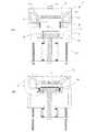
以下、図面を参照しながら本発明を詳細に説明する。図1は本発明に係る薄膜形成装置の好適実施例の断面略示図である。図1(A)はロードロック室(図示せず)から半導体基板を基板搬送チャンバ内に搬入した状態を示し、図1(B)は成膜反応時の装置状態を示している。
【0024】
本発明に係る薄膜形成装置1は反応チャンバ2及び基板搬送チャンバ3から成る。薄膜形成装置1の内部には半導体基板13を載置するためのサセプタ4が与えられ、該サセプタ4は昇降手段12によって、反応チャンバ2と基板搬送チャンバ3との間を上下に移動する。サセプタ4の内部には例えばシースヒータ(図示せず)のような加熱装置が埋設されており、半導体基板13を所望の温度(50〜500℃)に加熱する。サセプタ4の下部は半径方向に伸張した段部14を形成する。サセプタ4には3本から4本の基板リフトピン9が貫通しており、基板の搬送時には半導体基板13をサセプタ上方へ持ち上げる。サセプタ4は電気的に接地されており、一方の高周波電極を兼ねている。
【0025】
反応チャンバ2の天井部にはサセプタ4と対向して平行にシャワーヘッド6が設置されている。シャワーヘッド6には数千個の細孔10が設けられ、反応ガス導入口10から導入された反応ガスは該細孔10を通じて半導体基板13に均等に噴射される。シャワーヘッド6は外部の高周波電源(図示せず)に接続され、もう一方の高周波電極を兼ねている。シャワーヘッド6は所望の温度(50℃から500℃)に維持される。
【0026】
シャワーヘッド6の下部周辺には反応チャンバ2の側壁に沿って環状の排気ダクト手段5が設けられている。排気ダクト手段5は反応チャンバ2内でシャワーヘッド6を支持すると同時に、処理済の反応ガス若しくはパージガスを外部の真空ポンプ(図示せず)へ排出するための通路を提供する。排気ダクト手段5の周囲は絶縁体によって構成されている。
【0027】
排気ダクト手段5の底面17付近には、該排気ダクト手段5と同軸に円環状の分離板7が設けられている。分離板7は絶縁体から成る。以下で詳細に説明するように、排気ダクト手段5の底面17と、当該分離板7の上面との間には所定の間隔の隙間16が形成されており、反応空間15内のガスはこの隙間16を通じて排気ダクト手段5へ流れる。
【0028】
分離板7の底面には本発明に係る円筒状のベローズ手段8が分離板7と同軸に取り付けられている。図1(B)に示されるように、半導体基板13上に薄膜を形成するべくサセプタ4を反応位置まで上昇させるとき、サセプタの段部14と当該ベローズ手段8が係合し、ベローズが圧縮されてシールが達成される。このシールによって反応チャンバ2と基板搬送チャンバ3とは完全に分離され、反応空間15内の反応ガスが基板搬送チャンバ3内に侵入することはない。
【0029】
次に、本発明に係るベローズ手段8について詳細に説明する。図2(A)は図1(B)の部位aの拡大図を示し、図2(B)はベローズ手段8の斜視図を示す。サセプタ4が反応位置にある時、分離板7の上面24及びサセプタ4の上面23はアライメントされている。分離板7の側面25とサセプタ4の側面26との間には隙間22が画成される。隙間16及び隙間22の間隔は好適には0.2〜4mmであるが、分離板7の厚み及び幅を変えることによって自由に選択可能である。分離板7の底面21にはベローズ手段8の上端が溶接若しくはメタルガスケットにより取り付けられている。ベローズ手段8は300℃以上の高温に耐えかつ反応ガス及びそのラジカルと反応しないような耐熱及び耐腐食性金属から成る。そのような材料は代表的にはアルミニウムである。ベローズ手段8の下端にはシール用リング20が設けられている。シール用リング20の断面は好適には円であるが、それ以外に楕円、三角形、ひし形等であってもよい。また、シール用リング20が係合するサセプタ4の段部14の係合面には、シール用リングの断面形状に対応した溝が形成されていてもよい。シール用リング20が段部14と線接触することによってシールが達成され、隙間22を通過したガスは完全に遮断される。
【0030】
変形的に、ベローズ手段8の上端にシール用リング20が設けられ、ベローズ手段8の下端がサセプタ4の段部14に溶接若しくはメタルガスケットにより取り付けられることもできる。その際には、サセプタ4が反応位置まで上昇した時シール用リング20が分離板7の底面21に係合しシールが達成される。
【0031】
図2(C)は本発明に係るベローズ手段の変形例を示す。ベローズ手段8の側面には水平方向に伸長する略U字形の導電部材28が取り付けられている。導電部材28の先端は基板搬送チャンバの側壁27に接触している。側壁27は導体であるため、シールした際にサセプタ4と側壁27は電気的に導通状態となる。これによって、リアクタとサセプタとの電位差が解消される。その結果、サセプタ内のヒータのインピーダンスに起因する搬送チャンバ内での不所望なプラズマの発生が抑制される。導電部材28はベローズ手段8の円周の回りにひとつ若しくはそれ以上設けることができ、略U字形以外にあらゆる形状が可能である。
【0032】
図3は、本発明に係るシール手段の他の実施例を示す。図3(A)は本発明に係るシール手段であるO−リング状ガスケット30の断面図を示す。O−リング状ガスケット30は、管状のコイルスプリング32と、断面がC字型のアルミニウム被覆31から成る。図3(B)はO−リング状ガスケット30をリアクタ内に設置した状態を示す。他の実施例において、分離板38は水平部分33と該水平部分33の先端から垂直下方に伸長する側方部分34から成る。搬送チャンバの側壁は内側に伸張する突起部分35を有する。突起部分35の厚さはO−リング状ガスケットの断面直径よりやや薄く、図3(C)に示すシール状態の時、サセプタの段部14と該突起部分35の底面37が極めて近接するように調節されている。搬送チャンバ側壁の突起部分35の上面からは水平方向内側に向かってさらに突起部分36が伸長している。突起部分36はO−リング状ガスケット30のアルミニウム被覆31とほぼ等しい厚みを有する。O−リング状ガスケット30は搬送チャンバ側壁の突起部分35と分離板38の側方部分34との間に、コイルスプリング32が露出している方が外側になるように(すなわち、アルミニウム被覆されている方が反応ガスに晒されるように)挿入される。この時、突起部分36の先端はアルミニウム被覆31と係合し、両者は電気的に導通状態となる。
【0033】
図3(C)に示されるように、サセプタ4が反応位置まで上昇すると、O−リング状ガスケット30がサセプタ4の段部14と係合し圧縮されてシールが達成される。分離板38の表面とサセプタ4の表面はアライメントされ、分離板38の側方部分34とサセプタ4の側面との間に隙間39が画成される。該隙間39の間隔は好適には0.2〜4mmであるが、分離板38の水平部分33の幅若しくは側方部分34の幅を変えることにより調節可能である。隙間39を通過したガスは、O−リング状ガスケット30によって完全に遮断され、搬送チャンバ内に侵入することが防止される。また、サセプタ4の段部14とアルミニウム被覆31が係合することによって、サセプタ4、アルミニウム被覆31及び搬送チャンバ側壁が電気的に導通状態となり、サセプタ4と搬送チャンバ側壁との間に電位差が生じなくなる。その結果、サセプタ4内のヒータのインピーダンスに起因する搬送チャンバ内での不所望なプラズマの発生が抑制される。
【0034】
変形的に、O−リング状ガスケット30の下端がサセプタ4の段部14に溶接若しくはメタルガスケットにより取り付けられることもできる。その際には、サセプタ4が反応位置まで上昇した時O−リング状ガスケット30の上端が分離板38の底面に係合しシールが達成される。
【0035】
O−リング状ガスケット30の被覆材料として、アルミニウム以外に、耐熱及び耐腐食性金属材料を使用することも可能である。
【0036】
【効果】
本発明に従う薄膜形成装置により、反応エリアと搬送エリアとを完全に分離することができ、残留ガスのパージ時間を大幅に短縮することができるようになった。
【0037】
また、本発明に従う薄膜形成装置により、リアクタとサセプタとの間で電位差が生じなくなり、搬送チャンバ内に不所望なプラズマが発生することが無くなった。
【0038】
さらに、本発明に従う薄膜形成装置により、パージ時間の短縮に伴い生産性が向上し、パーティクル汚染が低減された結果信頼性の高い半導体装置を製造することができるようになった。
【図面の簡単な説明】
【図1】図1は、本発明に従う薄膜形成装置の断面略示図であり、図1(A)は基板搬送状態を示し、図1(B)は成膜反応状態を示す。
【図2】図2(A)は、図1(B)の部位aの拡大図を示し、図2(B)は本発明に係るベローズ手段を示し、図2(C)はベローズ手段の変形例を示す。
【図3】図3(A)は、本発明に係るシール手段の他の実施例を示し、図3(B)は該シール手段を装着した状態を示し、図3(C)は該シール手段によりシールされた状態を示す。
【符号の説明】
1 薄膜形成装置
2 反応チャンバ
3 基板搬送チャンバ
4 サセプタ
5 排気ダクト手段
6 シャワーヘッド
7 分離板
8 ベローズ手段
9 基板リフトピン
10 細孔
11 反応ガス導入口
12 昇降装置
13 半導体基板
14 段部
15 反応空間
16 隙間
17 底面[0001]
BACKGROUND OF THE INVENTION
The present invention relates to a film forming apparatus for forming a thin film on a semiconductor substrate, and more particularly, to a film forming apparatus that can completely separate a reaction chamber and a substrate transfer chamber.
[0002]
[Prior Art and Problems to be Solved by the Invention]
Along with the high integration of semiconductor devices, ALCVD (atomic layer CVD), which has good thin film formation controllability, has been attracting attention in place of the conventionally used CVD (chemical vapor deposition) method. ALCVD is designed to perform film formation using only the adsorption layer by alternately adsorbing multiple reaction gases used for film formation on a semiconductor wafer, so thin film control from several molecular levels is possible and step coverage is also possible. It is good.
[0003]
When performing an ALCVD process, it is important that the residual gas is exhausted completely from the reactor before switching the reaction gas. If the residual gas is present in the reactor, a CVD reaction occurs in the gas phase, making it difficult to control the film thickness at the molecular layer level. In addition, there is a problem that particles are generated when the particle diameter generated by the gas phase reaction is increased.
[0004]
Conventionally, in order to exhaust the residual gas completely from the reactor, a long purging step is required, resulting in a problem that productivity is lowered.
[0005]
Therefore, an attempt has been made to reduce the dead space by completely separating the reaction chamber area and the substrate transfer chamber area and to shorten the purge time for exhausting the residual gas. As one example, there is a method in which a susceptor on which a semiconductor wafer is placed is in physical contact with the reactor inner wall. However, in this method, it is difficult to make the susceptor and the contact partner parallel to each other, and the reaction chamber and the substrate transfer chamber cannot be completely separated. As another example, there is a method of sealing by providing an O-ring on the outer periphery of the susceptor. However, in this method, there is no problem when the process temperature is relatively low (about 200 ° C.), but when the temperature is high (300 ° C. or higher), the O-ring is damaged and cannot be used.
[0006]
As another method of purging the residual gas in the reactor, the process area is not separated completely from the reaction area and the transfer area, and a slight gap (about 0.5 mm) is provided to allow the inert gas to flow from the transfer area. A method has been devised to prevent wraparound (see, for example,
[0007]
[Patent Document 1]
US Pat. No. 4,854,263 Specification
[Patent Document 2]
Japanese Patent Laid-Open No. 2002-353207
With this method, it was not possible to completely prevent the reaction gas from flowing into the transfer area due to diffusion, and film formation by the CVD reaction was observed in the transfer area. This indicates that there is a risk of generation of particles because the residual gas of the reaction gas cannot be exhausted completely in addition to advancing the maintenance cycle. Moreover, it is difficult to shorten the purge time by this method.
[0010]
Furthermore, Japanese Patent Application No. 2001-361669 describes a method of separating a reaction chamber and a substrate transfer chamber by a gas seal. However, with the recent increase in the substrate diameter, there are an increasing number of processes that use higher high-frequency power having a higher frequency. In such a process, the impedance of the heater embedded in the susceptor cannot be ignored. As a result, when the potential difference between the grounded reactor and the susceptor becomes large and exceeds the ionization voltage of the seal gas, plasma discharge occurs between the transfer chamber and the lower part of the susceptor. A very small amount of film-forming gas diffusing from the reaction region undergoes a decomposition reaction in the plasma and adheres as a deposit to the transfer chamber wall or the gate valve that separates the load lock chamber and the transfer chamber. It may peel off and become a source of particle contamination.
[0011]
Accordingly, an object of the present invention is to provide a thin film forming apparatus capable of greatly reducing the purge time of residual gas by completely separating a reaction area and a transfer area.
[0012]
Another object of the present invention is to provide a thin film forming apparatus in which a potential difference does not occur between a grounded reactor and a susceptor.
[0013]
Another object of the present invention is to provide a thin film forming apparatus with high productivity and low risk of particle contamination.
[0014]
[Means for Solving the Problems]
In order to achieve the above object, a thin film forming apparatus according to the present invention comprises the following means.
[0015]
An apparatus for forming a thin film on a workpiece is as follows:
A reaction chamber;
A substrate transfer chamber;
A susceptor for placing and heating a workpiece, wherein the susceptor has a stepped portion extending in the radial direction;
Elevating means for raising and lowering the susceptor between the reaction chamber and the substrate transfer chamber;
A shower head in the reaction chamber, disposed in parallel with the susceptor and having a large number of pores for injecting a reaction gas toward the object to be processed;
Exhaust duct means annularly provided along the side wall of the reaction chamber around the lower portion of the showerhead to support the showerhead;
An annular separation plate coaxial with the exhaust duct means, installed near the bottom surface of the exhaust duct means and forming a predetermined gap with the bottom surface;
A cylindrical bellows means, which is attached to the bottom surface of the separation plate or the stepped surface of the susceptor and is coaxial with the separation plate, and a bellows means provided with a sealing ring at its tip,
Consisting of
When the susceptor is raised to the reaction position in the reaction chamber by the elevating means to form a thin film on the workpiece, the surface of the stepped portion or the bottom surface of the separation plate and the sealing ring of the bellows means are engaged to compress the bellows. And a seal is achieved.
[0016]
The bellows means is made of a heat-resistant and corrosion-resistant metal, and is joined to the bottom surface of the separation plate by welding or a metal gasket.
[0017]
Preferably, the bellows means is made of aluminum.
[0018]
Alternatively, the thin film forming apparatus according to the present invention may include a conductive member for electrically connecting the bellows means and the side wall of the substrate transfer chamber.
[0019]
In another aspect of the present invention, an apparatus for forming a thin film on an object to be processed includes:
A reaction chamber;
A substrate transfer chamber;
A susceptor for placing and heating a workpiece, wherein the susceptor has a stepped portion extending in the radial direction;
Elevating means for raising and lowering the susceptor between the reaction chamber and the substrate transfer chamber;
A shower head in the reaction chamber, disposed in parallel with the susceptor and having a large number of pores for injecting a reaction gas toward the object to be processed;
Exhaust duct means annularly provided along the side wall of the reaction chamber around the lower portion of the showerhead to support the showerhead;
An annular separation plate coaxial with the exhaust duct means, installed near the bottom surface of the exhaust duct means and forming a predetermined gap with the bottom surface;
An O-ring shaped gasket attached to the bottom surface of the separator plate or the surface of the susceptor step portion and having a C-shaped metal coating on a tubular coil spring;
Consisting of
When the susceptor is raised to the reaction position by the elevating means to form a thin film on the workpiece, the surface of the stepped portion or the bottom surface of the separation plate and the gasket are engaged and the gasket is compressed to achieve a seal. The susceptor and the substrate transfer chamber are electrically connected.
[0020]
Here, the gasket is attached to the bottom surface of the separation plate so that the exposed portion of the coil spring is in the outer peripheral direction, whereby the coil spring is prevented from contacting the reaction gas.
[0021]
Specifically, the metallic coating is made of a heat and corrosion resistant metal material.
[0022]
Preferably, the metallic coating consists of aluminum.
[0023]
BEST MODE FOR CARRYING OUT THE INVENTION
Hereinafter, the present invention will be described in detail with reference to the drawings. FIG. 1 is a schematic sectional view of a preferred embodiment of a thin film forming apparatus according to the present invention. FIG. 1A shows a state where a semiconductor substrate is carried into a substrate transfer chamber from a load lock chamber (not shown), and FIG. 1B shows an apparatus state during a film forming reaction.
[0024]
A thin
[0025]
On the ceiling of the reaction chamber 2, a shower head 6 is installed in parallel with the
[0026]
An annular exhaust duct means 5 is provided around the lower portion of the shower head 6 along the side wall of the reaction chamber 2. The exhaust duct means 5 supports the shower head 6 in the reaction chamber 2 and at the same time provides a passage for exhausting the processed reaction gas or purge gas to an external vacuum pump (not shown). The periphery of the exhaust duct means 5 is constituted by an insulator.
[0027]
In the vicinity of the
[0028]
A cylindrical bellows means 8 according to the present invention is attached to the bottom surface of the
[0029]
Next, the bellows means 8 according to the present invention will be described in detail. 2A shows an enlarged view of the part a in FIG. 1B, and FIG. 2B shows a perspective view of the bellows means 8. FIG. When the
[0030]
Alternatively, a sealing
[0031]
FIG. 2C shows a modification of the bellows means according to the present invention. A substantially U-shaped
[0032]
FIG. 3 shows another embodiment of the sealing means according to the present invention. FIG. 3A shows a cross-sectional view of an O-ring-shaped
[0033]
As shown in FIG. 3C, when the
[0034]
Alternatively, the lower end of the O-ring-shaped
[0035]
As a covering material for the O-
[0036]
【effect】
With the thin film forming apparatus according to the present invention, the reaction area and the transport area can be completely separated, and the purge time of the residual gas can be greatly shortened.
[0037]
In addition, the thin film forming apparatus according to the present invention eliminates the potential difference between the reactor and the susceptor, thereby preventing unwanted plasma from being generated in the transfer chamber.
[0038]
Furthermore, with the thin film forming apparatus according to the present invention, the productivity is improved with the shortening of the purge time, and the particle contamination is reduced. As a result, a highly reliable semiconductor device can be manufactured.
[Brief description of the drawings]
FIG. 1 is a schematic cross-sectional view of a thin film forming apparatus according to the present invention, FIG. 1 (A) shows a substrate transfer state, and FIG. 1 (B) shows a film formation reaction state.
2 (A) shows an enlarged view of a part a of FIG. 1 (B), FIG. 2 (B) shows bellows means according to the present invention, and FIG. 2 (C) shows deformation of the bellows means. An example is shown.
FIG. 3 (A) shows another embodiment of the sealing means according to the present invention, FIG. 3 (B) shows a state in which the sealing means is mounted, and FIG. 3 (C) shows the sealing means. Shows a sealed state.
[Explanation of symbols]
1 Thin film forming equipment
2 Reaction chamber
3 Substrate transfer chamber
4 Susceptor
5 Exhaust duct means
6 Shower head
7 Separation plate
8 Bellows means
9 Board lift pin
10 pores
11 Reactive gas inlet
12 Lifting device
13 Semiconductor substrate
14 steps
15 reaction space
16 Clearance
17 Bottom
Claims (8)
Translated fromJapanese反応チャンバと、
基板搬送チャンバと、
前記被処理体を載置しかつ加熱するためのサセプタであって、半径方向に伸張した段部を有するところのサセプタと、
前記反応チャンバと前記基板搬送チャンバとの間で前記サセプタを上下させるための昇降手段と、
前記反応チャンバ内にあって、前記サセプタと平行に対向して設置され、前記被処理体に向かって反応ガスを噴射するための多数の細孔を有するシャワーヘッドと、
前記シャワーヘッドの下部周辺にあって前記シャワーヘッドを支持するよう前記反応チャンバの側壁に沿って環状に設けられた排気ダクト手段と、
前記排気ダクト手段の底面付近にあって、前記底面と所定の隙間を形成するように設置された、前記排気ダクト手段と同軸の円環状の分離板と、
前記分離板の底面若しくは前記段部の表面に取り付けられた、前記分離板と同軸の円筒状のベローズ手段であって、その先端にシール用リングが設けられているところのベローズ手段と、
から成り、
前記被処理体上へ薄膜を形成するべく前記昇降手段により前記サセプタを前記反応チャンバ内の反応位置まで上昇させるとき、前記段部の表面若しくは前記分離板の底面と前記ベローズ手段のシール用リングとが係合し前記ベローズが圧縮されてシールが達成されることを特徴とする装置。An apparatus for forming a thin film on a workpiece,
A reaction chamber;
A substrate transfer chamber;
A susceptor for mounting and heating the object to be processed, the susceptor having a stepped portion extending in a radial direction;
Elevating means for raising and lowering the susceptor between the reaction chamber and the substrate transfer chamber;
A shower head which is in the reaction chamber and is disposed in parallel with the susceptor and has a large number of pores for injecting a reaction gas toward the object to be processed;
An exhaust duct means provided annularly along a side wall of the reaction chamber so as to support the shower head around the lower portion of the shower head;
An annular separation plate coaxial with the exhaust duct means, which is located near the bottom surface of the exhaust duct means and is formed so as to form a predetermined gap with the bottom surface;
Cylindrical bellows means coaxial with the separation plate, attached to the bottom surface of the separation plate or the surface of the stepped portion, and a bellows means provided with a sealing ring at the tip thereof;
Consisting of
When raising the susceptor to the reaction position in the reaction chamber by the elevating means to form a thin film on the object to be processed, the surface of the stepped portion or the bottom surface of the separation plate and the sealing ring of the bellows means And the bellows are compressed to achieve a seal.
反応チャンバと、
基板搬送チャンバと、
前記被処理体を載置しかつ加熱するためのサセプタであって、半径方向に伸張した段部を有するところのサセプタと、
前記反応チャンバと前記基板搬送チャンバとの間で前記サセプタを上下させるための昇降手段と、
前記反応チャンバ内にあって、前記サセプタと平行に対向して設置され、前記被処理体に向かって反応ガスを噴射するための多数の細孔を有するシャワーヘッドと、
前記シャワーヘッドの下部周辺にあって前記シャワーヘッドを支持するよう前記反応チャンバの側壁に沿って環状に設けられた排気ダクト手段と、
前記排気ダクト手段の底面付近にあって、前記底面と所定の隙間を形成するように設置された、前記排気ダクト手段と同軸の円環状の分離板と、
前記分離板の底面若しくは前記段部の表面に取り付けられた、管状のコイルスプリングに断面がC字型の金属製被覆を施したO−リング状のガスケットと、
から成り、
前記被処理体上へ薄膜を形成するべく前記昇降手段により前記サセプタを反応位置まで上昇させるとき、前記段部の表面若しくは前記分離板の底面と前記ガスケットとが係合し前記ガスケットが圧縮されてシールが達成されると同時に前記サセプタと前記基板搬送チャンバとが電気的に接続されることを特徴とする装置。An apparatus for forming a thin film on a workpiece,
A reaction chamber;
A substrate transfer chamber;
A susceptor for mounting and heating the object to be processed, the susceptor having a stepped portion extending in a radial direction;
Elevating means for raising and lowering the susceptor between the reaction chamber and the substrate transfer chamber;
A shower head which is in the reaction chamber and is disposed in parallel with the susceptor and has a large number of pores for injecting a reaction gas toward the object to be processed;
An exhaust duct means provided annularly along a side wall of the reaction chamber so as to support the shower head around the lower portion of the shower head;
An annular separation plate coaxial with the exhaust duct means, which is located near the bottom surface of the exhaust duct means and is formed so as to form a predetermined gap with the bottom surface;
An O-ring-shaped gasket attached to the bottom surface of the separation plate or the surface of the stepped portion and having a C-shaped metal coating on a tubular coil spring;
Consisting of
When the susceptor is raised to the reaction position by the elevating means to form a thin film on the object to be processed, the surface of the stepped portion or the bottom surface of the separation plate and the gasket are engaged and the gasket is compressed. The apparatus is characterized in that the susceptor and the substrate transfer chamber are electrically connected at the same time that a seal is achieved.
Priority Applications (2)
| Application Number | Priority Date | Filing Date | Title |
|---|---|---|---|
| JP2003132221AJP4152802B2 (en) | 2003-05-09 | 2003-05-09 | Thin film forming equipment |
| US10/841,794US7267725B2 (en) | 2003-05-09 | 2004-05-07 | Thin-film deposition apparatus |
Applications Claiming Priority (1)
| Application Number | Priority Date | Filing Date | Title |
|---|---|---|---|
| JP2003132221AJP4152802B2 (en) | 2003-05-09 | 2003-05-09 | Thin film forming equipment |
Publications (2)
| Publication Number | Publication Date |
|---|---|
| JP2004335892A JP2004335892A (en) | 2004-11-25 |
| JP4152802B2true JP4152802B2 (en) | 2008-09-17 |
Family
ID=33410611
Family Applications (1)
| Application Number | Title | Priority Date | Filing Date |
|---|---|---|---|
| JP2003132221AExpired - LifetimeJP4152802B2 (en) | 2003-05-09 | 2003-05-09 | Thin film forming equipment |
Country Status (2)
| Country | Link |
|---|---|
| US (1) | US7267725B2 (en) |
| JP (1) | JP4152802B2 (en) |
Families Citing this family (358)
| Publication number | Priority date | Publication date | Assignee | Title |
|---|---|---|---|---|
| US20070243317A1 (en)* | 2002-07-15 | 2007-10-18 | Du Bois Dale R | Thermal Processing System and Configurable Vertical Chamber |
| DE102004009772A1 (en)* | 2004-02-28 | 2005-09-15 | Aixtron Ag | CVD reactor with process chamber height stabilization |
| ATE543925T1 (en)* | 2004-11-24 | 2012-02-15 | Oerlikon Solar Ag | VACUUM TREATMENT CHAMBER FOR VERY LARGE SUBSTRATES |
| US20070116872A1 (en)* | 2005-11-18 | 2007-05-24 | Tokyo Electron Limited | Apparatus for thermal and plasma enhanced vapor deposition and method of operating |
| US20070116873A1 (en)* | 2005-11-18 | 2007-05-24 | Tokyo Electron Limited | Apparatus for thermal and plasma enhanced vapor deposition and method of operating |
| US8454749B2 (en)* | 2005-12-19 | 2013-06-04 | Tokyo Electron Limited | Method and system for sealing a first assembly to a second assembly of a processing system |
| US7654010B2 (en)* | 2006-02-23 | 2010-02-02 | Tokyo Electron Limited | Substrate processing system, substrate processing method, and storage medium |
| US20070218702A1 (en)* | 2006-03-15 | 2007-09-20 | Asm Japan K.K. | Semiconductor-processing apparatus with rotating susceptor |
| KR20080027009A (en)* | 2006-09-22 | 2008-03-26 | 에이에스엠지니텍코리아 주식회사 | Atomic layer deposition apparatus and multilayer film deposition method using the same |
| US20080241384A1 (en)* | 2007-04-02 | 2008-10-02 | Asm Genitech Korea Ltd. | Lateral flow deposition apparatus and method of depositing film by using the apparatus |
| DE102007063363B4 (en)* | 2007-05-21 | 2016-05-12 | Centrotherm Photovoltaics Ag | Device for doping and coating semiconductor material at low pressure |
| TWI349720B (en)* | 2007-05-30 | 2011-10-01 | Ind Tech Res Inst | A power-delivery mechanism and apparatus of plasma-enhanced chemical vapor deposition using the same |
| JP5347294B2 (en)* | 2007-09-12 | 2013-11-20 | 東京エレクトロン株式会社 | Film forming apparatus, film forming method, and storage medium |
| CN101971287A (en)* | 2007-11-08 | 2011-02-09 | 应用材料公司 | Electrode arrangement with movable shield |
| US8282735B2 (en)* | 2007-11-27 | 2012-10-09 | Asm Genitech Korea Ltd. | Atomic layer deposition apparatus |
| JP2009163911A (en)* | 2007-12-28 | 2009-07-23 | Hitachi High-Technologies Corp | Plasma processing equipment |
| JP5548841B2 (en)* | 2008-01-16 | 2014-07-16 | チャーム エンジニアリング シーオー エルティーディー | Substrate processing equipment |
| FR2930561B1 (en)* | 2008-04-28 | 2011-01-14 | Altatech Semiconductor | DEVICE AND METHOD FOR CHEMICAL TREATMENT IN STEAM PHASE. |
| JP2010150603A (en)* | 2008-12-25 | 2010-07-08 | Fuji Electric Systems Co Ltd | Thin film forming apparatus |
| JP2010161316A (en)* | 2009-01-09 | 2010-07-22 | Ulvac Japan Ltd | Plasma processing device |
| JP5018818B2 (en)* | 2009-04-01 | 2012-09-05 | パナソニック株式会社 | Plasma processing equipment |
| US9394608B2 (en) | 2009-04-06 | 2016-07-19 | Asm America, Inc. | Semiconductor processing reactor and components thereof |
| TWI514933B (en)* | 2009-08-12 | 2015-12-21 | Taiwan Semiconductor Mfg Co Ltd | Apparatus of generating planarized focusing plasma for deep etching |
| US8802201B2 (en) | 2009-08-14 | 2014-08-12 | Asm America, Inc. | Systems and methods for thin-film deposition of metal oxides using excited nitrogen-oxygen species |
| JP5432686B2 (en)* | 2009-12-03 | 2014-03-05 | 東京エレクトロン株式会社 | Plasma processing equipment |
| US20110244968A1 (en)* | 2010-03-30 | 2011-10-06 | Apex Dynamics, Inc. | Flexible Coupler |
| US8801950B2 (en) | 2011-03-07 | 2014-08-12 | Novellus Systems, Inc. | Reduction of a process volume of a processing chamber using a nested dynamic inert volume |
| JP5794456B2 (en)* | 2011-04-26 | 2015-10-14 | イーグル工業株式会社 | Welding bellows for semiconductor manufacturing equipment |
| US9147571B2 (en)* | 2011-04-26 | 2015-09-29 | Eagle Industry Co., Ltd. | Welded bellows for semiconductor manufacturing device |
| US20130023129A1 (en) | 2011-07-20 | 2013-01-24 | Asm America, Inc. | Pressure transmitter for a semiconductor processing environment |
| US9859142B2 (en) | 2011-10-20 | 2018-01-02 | Lam Research Corporation | Edge seal for lower electrode assembly |
| US9869392B2 (en) | 2011-10-20 | 2018-01-16 | Lam Research Corporation | Edge seal for lower electrode assembly |
| US9017481B1 (en) | 2011-10-28 | 2015-04-28 | Asm America, Inc. | Process feed management for semiconductor substrate processing |
| US8900364B2 (en)* | 2011-11-29 | 2014-12-02 | Intermolecular, Inc. | High productivity vapor processing system |
| KR101378083B1 (en)* | 2012-06-14 | 2014-03-27 | 주식회사 수앤테크 | Wafer processing apparatus |
| US10714315B2 (en) | 2012-10-12 | 2020-07-14 | Asm Ip Holdings B.V. | Semiconductor reaction chamber showerhead |
| US20160376700A1 (en) | 2013-02-01 | 2016-12-29 | Asm Ip Holding B.V. | System for treatment of deposition reactor |
| US9957615B2 (en) | 2013-09-13 | 2018-05-01 | Applied Materials, Inc. | Apparatus to improve substrate temperature uniformity |
| CN103498192B (en)* | 2013-09-29 | 2016-07-06 | 青岛赛瑞达电子科技有限公司 | Double CVD stove |
| KR102293092B1 (en)* | 2013-11-12 | 2021-08-23 | 도쿄엘렉트론가부시키가이샤 | Plasma processing apparatus |
| US10090211B2 (en)* | 2013-12-26 | 2018-10-02 | Lam Research Corporation | Edge seal for lower electrode assembly |
| US11015245B2 (en) | 2014-03-19 | 2021-05-25 | Asm Ip Holding B.V. | Gas-phase reactor and system having exhaust plenum and components thereof |
| US10858737B2 (en) | 2014-07-28 | 2020-12-08 | Asm Ip Holding B.V. | Showerhead assembly and components thereof |
| US9890456B2 (en) | 2014-08-21 | 2018-02-13 | Asm Ip Holding B.V. | Method and system for in situ formation of gas-phase compounds |
| US10941490B2 (en) | 2014-10-07 | 2021-03-09 | Asm Ip Holding B.V. | Multiple temperature range susceptor, assembly, reactor and system including the susceptor, and methods of using the same |
| US10276355B2 (en) | 2015-03-12 | 2019-04-30 | Asm Ip Holding B.V. | Multi-zone reactor, system including the reactor, and method of using the same |
| US10597779B2 (en)* | 2015-06-05 | 2020-03-24 | Applied Materials, Inc. | Susceptor position and rational apparatus and methods of use |
| US10458018B2 (en) | 2015-06-26 | 2019-10-29 | Asm Ip Holding B.V. | Structures including metal carbide material, devices including the structures, and methods of forming same |
| US11421321B2 (en)* | 2015-07-28 | 2022-08-23 | Asm Ip Holding B.V. | Apparatuses for thin film deposition |
| US10211308B2 (en) | 2015-10-21 | 2019-02-19 | Asm Ip Holding B.V. | NbMC layers |
| US10358721B2 (en)* | 2015-10-22 | 2019-07-23 | Asm Ip Holding B.V. | Semiconductor manufacturing system including deposition apparatus |
| US11139308B2 (en) | 2015-12-29 | 2021-10-05 | Asm Ip Holding B.V. | Atomic layer deposition of III-V compounds to form V-NAND devices |
| US10529554B2 (en) | 2016-02-19 | 2020-01-07 | Asm Ip Holding B.V. | Method for forming silicon nitride film selectively on sidewalls or flat surfaces of trenches |
| US10343920B2 (en) | 2016-03-18 | 2019-07-09 | Asm Ip Holding B.V. | Aligned carbon nanotubes |
| US10190213B2 (en) | 2016-04-21 | 2019-01-29 | Asm Ip Holding B.V. | Deposition of metal borides |
| US10865475B2 (en) | 2016-04-21 | 2020-12-15 | Asm Ip Holding B.V. | Deposition of metal borides and silicides |
| US10367080B2 (en) | 2016-05-02 | 2019-07-30 | Asm Ip Holding B.V. | Method of forming a germanium oxynitride film |
| US11453943B2 (en) | 2016-05-25 | 2022-09-27 | Asm Ip Holding B.V. | Method for forming carbon-containing silicon/metal oxide or nitride film by ALD using silicon precursor and hydrocarbon precursor |
| US9859151B1 (en) | 2016-07-08 | 2018-01-02 | Asm Ip Holding B.V. | Selective film deposition method to form air gaps |
| US10612137B2 (en) | 2016-07-08 | 2020-04-07 | Asm Ip Holdings B.V. | Organic reactants for atomic layer deposition |
| KR102532607B1 (en) | 2016-07-28 | 2023-05-15 | 에이에스엠 아이피 홀딩 비.브이. | Substrate processing apparatus and method of operating the same |
| US9812320B1 (en) | 2016-07-28 | 2017-11-07 | Asm Ip Holding B.V. | Method and apparatus for filling a gap |
| US9887082B1 (en) | 2016-07-28 | 2018-02-06 | Asm Ip Holding B.V. | Method and apparatus for filling a gap |
| JP6794184B2 (en)* | 2016-08-31 | 2020-12-02 | 株式会社日本製鋼所 | Plasma atomic layer deposition equipment |
| JP6778553B2 (en)* | 2016-08-31 | 2020-11-04 | 株式会社日本製鋼所 | Atomic layer growth device and atomic layer growth method |
| JP6473974B2 (en)* | 2016-09-30 | 2019-02-27 | パナソニックIpマネジメント株式会社 | Plasma processing apparatus and plasma processing method |
| US10643826B2 (en) | 2016-10-26 | 2020-05-05 | Asm Ip Holdings B.V. | Methods for thermally calibrating reaction chambers |
| US11532757B2 (en) | 2016-10-27 | 2022-12-20 | Asm Ip Holding B.V. | Deposition of charge trapping layers |
| US10229833B2 (en) | 2016-11-01 | 2019-03-12 | Asm Ip Holding B.V. | Methods for forming a transition metal nitride film on a substrate by atomic layer deposition and related semiconductor device structures |
| US10714350B2 (en) | 2016-11-01 | 2020-07-14 | ASM IP Holdings, B.V. | Methods for forming a transition metal niobium nitride film on a substrate by atomic layer deposition and related semiconductor device structures |
| KR102546317B1 (en) | 2016-11-15 | 2023-06-21 | 에이에스엠 아이피 홀딩 비.브이. | Gas supply unit and substrate processing apparatus including the same |
| KR102762543B1 (en) | 2016-12-14 | 2025-02-05 | 에이에스엠 아이피 홀딩 비.브이. | Substrate processing apparatus |
| US11581186B2 (en) | 2016-12-15 | 2023-02-14 | Asm Ip Holding B.V. | Sequential infiltration synthesis apparatus |
| US11447861B2 (en) | 2016-12-15 | 2022-09-20 | Asm Ip Holding B.V. | Sequential infiltration synthesis apparatus and a method of forming a patterned structure |
| KR102700194B1 (en)* | 2016-12-19 | 2024-08-28 | 에이에스엠 아이피 홀딩 비.브이. | Substrate processing apparatus |
| US10269558B2 (en) | 2016-12-22 | 2019-04-23 | Asm Ip Holding B.V. | Method of forming a structure on a substrate |
| US10867788B2 (en) | 2016-12-28 | 2020-12-15 | Asm Ip Holding B.V. | Method of forming a structure on a substrate |
| US11390950B2 (en) | 2017-01-10 | 2022-07-19 | Asm Ip Holding B.V. | Reactor system and method to reduce residue buildup during a film deposition process |
| US10468261B2 (en) | 2017-02-15 | 2019-11-05 | Asm Ip Holding B.V. | Methods for forming a metallic film on a substrate by cyclical deposition and related semiconductor device structures |
| US10529563B2 (en) | 2017-03-29 | 2020-01-07 | Asm Ip Holdings B.V. | Method for forming doped metal oxide films on a substrate by cyclical deposition and related semiconductor device structures |
| KR102457289B1 (en) | 2017-04-25 | 2022-10-21 | 에이에스엠 아이피 홀딩 비.브이. | Method for depositing a thin film and manufacturing a semiconductor device |
| US10770286B2 (en) | 2017-05-08 | 2020-09-08 | Asm Ip Holdings B.V. | Methods for selectively forming a silicon nitride film on a substrate and related semiconductor device structures |
| US10892156B2 (en) | 2017-05-08 | 2021-01-12 | Asm Ip Holding B.V. | Methods for forming a silicon nitride film on a substrate and related semiconductor device structures |
| US10886123B2 (en) | 2017-06-02 | 2021-01-05 | Asm Ip Holding B.V. | Methods for forming low temperature semiconductor layers and related semiconductor device structures |
| US12040200B2 (en) | 2017-06-20 | 2024-07-16 | Asm Ip Holding B.V. | Semiconductor processing apparatus and methods for calibrating a semiconductor processing apparatus |
| US11306395B2 (en) | 2017-06-28 | 2022-04-19 | Asm Ip Holding B.V. | Methods for depositing a transition metal nitride film on a substrate by atomic layer deposition and related deposition apparatus |
| KR20190009245A (en) | 2017-07-18 | 2019-01-28 | 에이에스엠 아이피 홀딩 비.브이. | Methods for forming a semiconductor device structure and related semiconductor device structures |
| US11374112B2 (en) | 2017-07-19 | 2022-06-28 | Asm Ip Holding B.V. | Method for depositing a group IV semiconductor and related semiconductor device structures |
| US11018002B2 (en) | 2017-07-19 | 2021-05-25 | Asm Ip Holding B.V. | Method for selectively depositing a Group IV semiconductor and related semiconductor device structures |
| US10541333B2 (en) | 2017-07-19 | 2020-01-21 | Asm Ip Holding B.V. | Method for depositing a group IV semiconductor and related semiconductor device structures |
| US10590535B2 (en) | 2017-07-26 | 2020-03-17 | Asm Ip Holdings B.V. | Chemical treatment, deposition and/or infiltration apparatus and method for using the same |
| TWI815813B (en) | 2017-08-04 | 2023-09-21 | 荷蘭商Asm智慧財產控股公司 | Showerhead assembly for distributing a gas within a reaction chamber |
| US10770336B2 (en) | 2017-08-08 | 2020-09-08 | Asm Ip Holding B.V. | Substrate lift mechanism and reactor including same |
| US10692741B2 (en) | 2017-08-08 | 2020-06-23 | Asm Ip Holdings B.V. | Radiation shield |
| US11769682B2 (en) | 2017-08-09 | 2023-09-26 | Asm Ip Holding B.V. | Storage apparatus for storing cassettes for substrates and processing apparatus equipped therewith |
| US11139191B2 (en) | 2017-08-09 | 2021-10-05 | Asm Ip Holding B.V. | Storage apparatus for storing cassettes for substrates and processing apparatus equipped therewith |
| US11830730B2 (en) | 2017-08-29 | 2023-11-28 | Asm Ip Holding B.V. | Layer forming method and apparatus |
| US11295980B2 (en) | 2017-08-30 | 2022-04-05 | Asm Ip Holding B.V. | Methods for depositing a molybdenum metal film over a dielectric surface of a substrate by a cyclical deposition process and related semiconductor device structures |
| US11056344B2 (en) | 2017-08-30 | 2021-07-06 | Asm Ip Holding B.V. | Layer forming method |
| KR102491945B1 (en) | 2017-08-30 | 2023-01-26 | 에이에스엠 아이피 홀딩 비.브이. | Substrate processing apparatus |
| KR102401446B1 (en) | 2017-08-31 | 2022-05-24 | 에이에스엠 아이피 홀딩 비.브이. | Substrate processing apparatus |
| JP2019054189A (en) | 2017-09-19 | 2019-04-04 | 東芝メモリ株式会社 | Deposition device and deposition method |
| KR102630301B1 (en) | 2017-09-21 | 2024-01-29 | 에이에스엠 아이피 홀딩 비.브이. | Method of sequential infiltration synthesis treatment of infiltrateable material and structures and devices formed using same |
| US10844484B2 (en) | 2017-09-22 | 2020-11-24 | Asm Ip Holding B.V. | Apparatus for dispensing a vapor phase reactant to a reaction chamber and related methods |
| US10658205B2 (en) | 2017-09-28 | 2020-05-19 | Asm Ip Holdings B.V. | Chemical dispensing apparatus and methods for dispensing a chemical to a reaction chamber |
| US10403504B2 (en) | 2017-10-05 | 2019-09-03 | Asm Ip Holding B.V. | Method for selectively depositing a metallic film on a substrate |
| US10923344B2 (en) | 2017-10-30 | 2021-02-16 | Asm Ip Holding B.V. | Methods for forming a semiconductor structure and related semiconductor structures |
| US10872803B2 (en) | 2017-11-03 | 2020-12-22 | Asm Ip Holding B.V. | Apparatus and methods for isolating a reaction chamber from a loading chamber resulting in reduced contamination |
| US10872804B2 (en)* | 2017-11-03 | 2020-12-22 | Asm Ip Holding B.V. | Apparatus and methods for isolating a reaction chamber from a loading chamber resulting in reduced contamination |
| US10910262B2 (en) | 2017-11-16 | 2021-02-02 | Asm Ip Holding B.V. | Method of selectively depositing a capping layer structure on a semiconductor device structure |
| US11022879B2 (en) | 2017-11-24 | 2021-06-01 | Asm Ip Holding B.V. | Method of forming an enhanced unexposed photoresist layer |
| CN111344522B (en) | 2017-11-27 | 2022-04-12 | 阿斯莫Ip控股公司 | Including clean mini-environment device |
| WO2019103613A1 (en) | 2017-11-27 | 2019-05-31 | Asm Ip Holding B.V. | A storage device for storing wafer cassettes for use with a batch furnace |
| US10872771B2 (en) | 2018-01-16 | 2020-12-22 | Asm Ip Holding B. V. | Method for depositing a material film on a substrate within a reaction chamber by a cyclical deposition process and related device structures |
| KR102695659B1 (en) | 2018-01-19 | 2024-08-14 | 에이에스엠 아이피 홀딩 비.브이. | Method for depositing a gap filling layer by plasma assisted deposition |
| TWI799494B (en) | 2018-01-19 | 2023-04-21 | 荷蘭商Asm 智慧財產控股公司 | Deposition method |
| US11018047B2 (en) | 2018-01-25 | 2021-05-25 | Asm Ip Holding B.V. | Hybrid lift pin |
| USD880437S1 (en) | 2018-02-01 | 2020-04-07 | Asm Ip Holding B.V. | Gas supply plate for semiconductor manufacturing apparatus |
| US11081345B2 (en) | 2018-02-06 | 2021-08-03 | Asm Ip Holding B.V. | Method of post-deposition treatment for silicon oxide film |
| WO2019158960A1 (en) | 2018-02-14 | 2019-08-22 | Asm Ip Holding B.V. | A method for depositing a ruthenium-containing film on a substrate by a cyclical deposition process |
| US10896820B2 (en) | 2018-02-14 | 2021-01-19 | Asm Ip Holding B.V. | Method for depositing a ruthenium-containing film on a substrate by a cyclical deposition process |
| JP7061889B2 (en)* | 2018-02-15 | 2022-05-02 | 東京エレクトロン株式会社 | Placement device and processing device for the object to be processed |
| US10731249B2 (en) | 2018-02-15 | 2020-08-04 | Asm Ip Holding B.V. | Method of forming a transition metal containing film on a substrate by a cyclical deposition process, a method for supplying a transition metal halide compound to a reaction chamber, and related vapor deposition apparatus |
| KR102636427B1 (en) | 2018-02-20 | 2024-02-13 | 에이에스엠 아이피 홀딩 비.브이. | Substrate processing method and apparatus |
| US10975470B2 (en) | 2018-02-23 | 2021-04-13 | Asm Ip Holding B.V. | Apparatus for detecting or monitoring for a chemical precursor in a high temperature environment |
| US11473195B2 (en) | 2018-03-01 | 2022-10-18 | Asm Ip Holding B.V. | Semiconductor processing apparatus and a method for processing a substrate |
| US11629406B2 (en) | 2018-03-09 | 2023-04-18 | Asm Ip Holding B.V. | Semiconductor processing apparatus comprising one or more pyrometers for measuring a temperature of a substrate during transfer of the substrate |
| US11114283B2 (en) | 2018-03-16 | 2021-09-07 | Asm Ip Holding B.V. | Reactor, system including the reactor, and methods of manufacturing and using same |
| KR102646467B1 (en) | 2018-03-27 | 2024-03-11 | 에이에스엠 아이피 홀딩 비.브이. | Method of forming an electrode on a substrate and a semiconductor device structure including an electrode |
| US11230766B2 (en) | 2018-03-29 | 2022-01-25 | Asm Ip Holding B.V. | Substrate processing apparatus and method |
| US11088002B2 (en) | 2018-03-29 | 2021-08-10 | Asm Ip Holding B.V. | Substrate rack and a substrate processing system and method |
| KR102501472B1 (en) | 2018-03-30 | 2023-02-20 | 에이에스엠 아이피 홀딩 비.브이. | Substrate processing method |
| KR102600229B1 (en) | 2018-04-09 | 2023-11-10 | 에이에스엠 아이피 홀딩 비.브이. | Substrate supporting device, substrate processing apparatus including the same and substrate processing method |
| US12025484B2 (en) | 2018-05-08 | 2024-07-02 | Asm Ip Holding B.V. | Thin film forming method |
| TWI811348B (en) | 2018-05-08 | 2023-08-11 | 荷蘭商Asm 智慧財產控股公司 | Methods for depositing an oxide film on a substrate by a cyclical deposition process and related device structures |
| US12272527B2 (en) | 2018-05-09 | 2025-04-08 | Asm Ip Holding B.V. | Apparatus for use with hydrogen radicals and method of using same |
| KR20190129718A (en) | 2018-05-11 | 2019-11-20 | 에이에스엠 아이피 홀딩 비.브이. | Methods for forming a doped metal carbide film on a substrate and related semiconductor device structures |
| US11434569B2 (en)* | 2018-05-25 | 2022-09-06 | Applied Materials, Inc. | Ground path systems for providing a shorter and symmetrical ground path |
| KR102596988B1 (en) | 2018-05-28 | 2023-10-31 | 에이에스엠 아이피 홀딩 비.브이. | Method of processing a substrate and a device manufactured by the same |
| TWI840362B (en) | 2018-06-04 | 2024-05-01 | 荷蘭商Asm Ip私人控股有限公司 | Wafer handling chamber with moisture reduction |
| US11718913B2 (en) | 2018-06-04 | 2023-08-08 | Asm Ip Holding B.V. | Gas distribution system and reactor system including same |
| US11286562B2 (en) | 2018-06-08 | 2022-03-29 | Asm Ip Holding B.V. | Gas-phase chemical reactor and method of using same |
| US10797133B2 (en) | 2018-06-21 | 2020-10-06 | Asm Ip Holding B.V. | Method for depositing a phosphorus doped silicon arsenide film and related semiconductor device structures |
| KR102568797B1 (en) | 2018-06-21 | 2023-08-21 | 에이에스엠 아이피 홀딩 비.브이. | Substrate processing system |
| TWI873894B (en) | 2018-06-27 | 2025-02-21 | 荷蘭商Asm Ip私人控股有限公司 | Cyclic deposition methods for forming metal-containing material and films and structures including the metal-containing material |
| KR102854019B1 (en) | 2018-06-27 | 2025-09-02 | 에이에스엠 아이피 홀딩 비.브이. | Periodic deposition method for forming a metal-containing material and films and structures comprising the metal-containing material |
| US10612136B2 (en) | 2018-06-29 | 2020-04-07 | ASM IP Holding, B.V. | Temperature-controlled flange and reactor system including same |
| KR102686758B1 (en) | 2018-06-29 | 2024-07-18 | 에이에스엠 아이피 홀딩 비.브이. | Method for depositing a thin film and manufacturing a semiconductor device |
| US10388513B1 (en) | 2018-07-03 | 2019-08-20 | Asm Ip Holding B.V. | Method for depositing silicon-free carbon-containing film as gap-fill layer by pulse plasma-assisted deposition |
| US10755922B2 (en) | 2018-07-03 | 2020-08-25 | Asm Ip Holding B.V. | Method for depositing silicon-free carbon-containing film as gap-fill layer by pulse plasma-assisted deposition |
| US10767789B2 (en) | 2018-07-16 | 2020-09-08 | Asm Ip Holding B.V. | Diaphragm valves, valve components, and methods for forming valve components |
| US11053591B2 (en) | 2018-08-06 | 2021-07-06 | Asm Ip Holding B.V. | Multi-port gas injection system and reactor system including same |
| US10883175B2 (en) | 2018-08-09 | 2021-01-05 | Asm Ip Holding B.V. | Vertical furnace for processing substrates and a liner for use therein |
| US10829852B2 (en) | 2018-08-16 | 2020-11-10 | Asm Ip Holding B.V. | Gas distribution device for a wafer processing apparatus |
| US11430674B2 (en) | 2018-08-22 | 2022-08-30 | Asm Ip Holding B.V. | Sensor array, apparatus for dispensing a vapor phase reactant to a reaction chamber and related methods |
| US11024523B2 (en) | 2018-09-11 | 2021-06-01 | Asm Ip Holding B.V. | Substrate processing apparatus and method |
| KR102707956B1 (en) | 2018-09-11 | 2024-09-19 | 에이에스엠 아이피 홀딩 비.브이. | Method for deposition of a thin film |
| US11049751B2 (en) | 2018-09-14 | 2021-06-29 | Asm Ip Holding B.V. | Cassette supply system to store and handle cassettes and processing apparatus equipped therewith |
| JP7209247B2 (en)* | 2018-09-25 | 2023-01-20 | パナソニックIpマネジメント株式会社 | Element chip manufacturing method |
| CN110970344B (en) | 2018-10-01 | 2024-10-25 | Asmip控股有限公司 | Substrate holding apparatus, system comprising the same and method of using the same |
| US11232963B2 (en) | 2018-10-03 | 2022-01-25 | Asm Ip Holding B.V. | Substrate processing apparatus and method |
| KR102592699B1 (en) | 2018-10-08 | 2023-10-23 | 에이에스엠 아이피 홀딩 비.브이. | Substrate support unit and apparatuses for depositing thin film and processing the substrate including the same |
| KR102605121B1 (en) | 2018-10-19 | 2023-11-23 | 에이에스엠 아이피 홀딩 비.브이. | Substrate processing apparatus and substrate processing method |
| KR102546322B1 (en) | 2018-10-19 | 2023-06-21 | 에이에스엠 아이피 홀딩 비.브이. | Substrate processing apparatus and substrate processing method |
| USD948463S1 (en) | 2018-10-24 | 2022-04-12 | Asm Ip Holding B.V. | Susceptor for semiconductor substrate supporting apparatus |
| US12378665B2 (en) | 2018-10-26 | 2025-08-05 | Asm Ip Holding B.V. | High temperature coatings for a preclean and etch apparatus and related methods |
| US11087997B2 (en) | 2018-10-31 | 2021-08-10 | Asm Ip Holding B.V. | Substrate processing apparatus for processing substrates |
| KR102748291B1 (en) | 2018-11-02 | 2024-12-31 | 에이에스엠 아이피 홀딩 비.브이. | Substrate support unit and substrate processing apparatus including the same |
| US11572620B2 (en) | 2018-11-06 | 2023-02-07 | Asm Ip Holding B.V. | Methods for selectively depositing an amorphous silicon film on a substrate |
| US11031242B2 (en) | 2018-11-07 | 2021-06-08 | Asm Ip Holding B.V. | Methods for depositing a boron doped silicon germanium film |
| US10847366B2 (en) | 2018-11-16 | 2020-11-24 | Asm Ip Holding B.V. | Methods for depositing a transition metal chalcogenide film on a substrate by a cyclical deposition process |
| US10818758B2 (en) | 2018-11-16 | 2020-10-27 | Asm Ip Holding B.V. | Methods for forming a metal silicate film on a substrate in a reaction chamber and related semiconductor device structures |
| US12040199B2 (en) | 2018-11-28 | 2024-07-16 | Asm Ip Holding B.V. | Substrate processing apparatus for processing substrates |
| US11217444B2 (en) | 2018-11-30 | 2022-01-04 | Asm Ip Holding B.V. | Method for forming an ultraviolet radiation responsive metal oxide-containing film |
| KR102636428B1 (en) | 2018-12-04 | 2024-02-13 | 에이에스엠 아이피 홀딩 비.브이. | A method for cleaning a substrate processing apparatus |
| US11158513B2 (en) | 2018-12-13 | 2021-10-26 | Asm Ip Holding B.V. | Methods for forming a rhenium-containing film on a substrate by a cyclical deposition process and related semiconductor device structures |
| TWI874340B (en) | 2018-12-14 | 2025-03-01 | 荷蘭商Asm Ip私人控股有限公司 | Method of forming device structure, structure formed by the method and system for performing the method |
| TWI866480B (en) | 2019-01-17 | 2024-12-11 | 荷蘭商Asm Ip 私人控股有限公司 | Methods of forming a transition metal containing film on a substrate by a cyclical deposition process |
| KR102727227B1 (en) | 2019-01-22 | 2024-11-07 | 에이에스엠 아이피 홀딩 비.브이. | Semiconductor processing device |
| CN111524788B (en) | 2019-02-01 | 2023-11-24 | Asm Ip私人控股有限公司 | Method for forming topologically selective films of silicon oxide |
| TWI838458B (en) | 2019-02-20 | 2024-04-11 | 荷蘭商Asm Ip私人控股有限公司 | Apparatus and methods for plug fill deposition in 3-d nand applications |
| TWI873122B (en) | 2019-02-20 | 2025-02-21 | 荷蘭商Asm Ip私人控股有限公司 | Method of filling a recess formed within a surface of a substrate, semiconductor structure formed according to the method, and semiconductor processing apparatus |
| TWI845607B (en) | 2019-02-20 | 2024-06-21 | 荷蘭商Asm Ip私人控股有限公司 | Cyclical deposition method and apparatus for filling a recess formed within a substrate surface |
| KR102626263B1 (en) | 2019-02-20 | 2024-01-16 | 에이에스엠 아이피 홀딩 비.브이. | Cyclical deposition method including treatment step and apparatus for same |
| TWI842826B (en) | 2019-02-22 | 2024-05-21 | 荷蘭商Asm Ip私人控股有限公司 | Substrate processing apparatus and method for processing substrate |
| KR102858005B1 (en) | 2019-03-08 | 2025-09-09 | 에이에스엠 아이피 홀딩 비.브이. | Method for Selective Deposition of Silicon Nitride Layer and Structure Including Selectively-Deposited Silicon Nitride Layer |
| KR102782593B1 (en) | 2019-03-08 | 2025-03-14 | 에이에스엠 아이피 홀딩 비.브이. | Structure Including SiOC Layer and Method of Forming Same |
| US11742198B2 (en) | 2019-03-08 | 2023-08-29 | Asm Ip Holding B.V. | Structure including SiOCN layer and method of forming same |
| JP2020167398A (en) | 2019-03-28 | 2020-10-08 | エーエスエム・アイピー・ホールディング・ベー・フェー | Door openers and substrate processing equipment provided with door openers |
| KR102809999B1 (en) | 2019-04-01 | 2025-05-19 | 에이에스엠 아이피 홀딩 비.브이. | Method of manufacturing semiconductor device |
| KR20200123380A (en) | 2019-04-19 | 2020-10-29 | 에이에스엠 아이피 홀딩 비.브이. | Layer forming method and apparatus |
| KR20200125453A (en) | 2019-04-24 | 2020-11-04 | 에이에스엠 아이피 홀딩 비.브이. | Gas-phase reactor system and method of using same |
| KR20200130121A (en) | 2019-05-07 | 2020-11-18 | 에이에스엠 아이피 홀딩 비.브이. | Chemical source vessel with dip tube |
| US11289326B2 (en) | 2019-05-07 | 2022-03-29 | Asm Ip Holding B.V. | Method for reforming amorphous carbon polymer film |
| KR20200130652A (en) | 2019-05-10 | 2020-11-19 | 에이에스엠 아이피 홀딩 비.브이. | Method of depositing material onto a surface and structure formed according to the method |
| JP7612342B2 (en) | 2019-05-16 | 2025-01-14 | エーエスエム・アイピー・ホールディング・ベー・フェー | Wafer boat handling apparatus, vertical batch furnace and method |
| JP7598201B2 (en) | 2019-05-16 | 2024-12-11 | エーエスエム・アイピー・ホールディング・ベー・フェー | Wafer boat handling apparatus, vertical batch furnace and method |
| USD947913S1 (en) | 2019-05-17 | 2022-04-05 | Asm Ip Holding B.V. | Susceptor shaft |
| USD975665S1 (en) | 2019-05-17 | 2023-01-17 | Asm Ip Holding B.V. | Susceptor shaft |
| USD935572S1 (en) | 2019-05-24 | 2021-11-09 | Asm Ip Holding B.V. | Gas channel plate |
| USD922229S1 (en) | 2019-06-05 | 2021-06-15 | Asm Ip Holding B.V. | Device for controlling a temperature of a gas supply unit |
| KR20200141002A (en) | 2019-06-06 | 2020-12-17 | 에이에스엠 아이피 홀딩 비.브이. | Method of using a gas-phase reactor system including analyzing exhausted gas |
| KR20200141931A (en) | 2019-06-10 | 2020-12-21 | 에이에스엠 아이피 홀딩 비.브이. | Method for cleaning quartz epitaxial chambers |
| KR20200143254A (en) | 2019-06-11 | 2020-12-23 | 에이에스엠 아이피 홀딩 비.브이. | Method of forming an electronic structure using an reforming gas, system for performing the method, and structure formed using the method |
| USD944946S1 (en) | 2019-06-14 | 2022-03-01 | Asm Ip Holding B.V. | Shower plate |
| USD931978S1 (en) | 2019-06-27 | 2021-09-28 | Asm Ip Holding B.V. | Showerhead vacuum transport |
| KR20210005515A (en) | 2019-07-03 | 2021-01-14 | 에이에스엠 아이피 홀딩 비.브이. | Temperature control assembly for substrate processing apparatus and method of using same |
| JP7499079B2 (en) | 2019-07-09 | 2024-06-13 | エーエスエム・アイピー・ホールディング・ベー・フェー | Plasma device using coaxial waveguide and substrate processing method |
| CN112216646A (en) | 2019-07-10 | 2021-01-12 | Asm Ip私人控股有限公司 | Substrate supporting assembly and substrate processing device comprising same |
| KR20210010307A (en) | 2019-07-16 | 2021-01-27 | 에이에스엠 아이피 홀딩 비.브이. | Substrate processing apparatus |
| KR102860110B1 (en) | 2019-07-17 | 2025-09-16 | 에이에스엠 아이피 홀딩 비.브이. | Methods of forming silicon germanium structures |
| KR20210010816A (en) | 2019-07-17 | 2021-01-28 | 에이에스엠 아이피 홀딩 비.브이. | Radical assist ignition plasma system and method |
| US11643724B2 (en) | 2019-07-18 | 2023-05-09 | Asm Ip Holding B.V. | Method of forming structures using a neutral beam |
| TWI839544B (en) | 2019-07-19 | 2024-04-21 | 荷蘭商Asm Ip私人控股有限公司 | Method of forming topology-controlled amorphous carbon polymer film |
| KR20210010817A (en) | 2019-07-19 | 2021-01-28 | 에이에스엠 아이피 홀딩 비.브이. | Method of Forming Topology-Controlled Amorphous Carbon Polymer Film |
| TWI851767B (en) | 2019-07-29 | 2024-08-11 | 荷蘭商Asm Ip私人控股有限公司 | Methods for selective deposition utilizing n-type dopants and/or alternative dopants to achieve high dopant incorporation |
| CN112309899A (en) | 2019-07-30 | 2021-02-02 | Asm Ip私人控股有限公司 | Substrate processing apparatus |
| CN112309900A (en) | 2019-07-30 | 2021-02-02 | Asm Ip私人控股有限公司 | Substrate processing apparatus |
| US12169361B2 (en) | 2019-07-30 | 2024-12-17 | Asm Ip Holding B.V. | Substrate processing apparatus and method |
| US11587814B2 (en) | 2019-07-31 | 2023-02-21 | Asm Ip Holding B.V. | Vertical batch furnace assembly |
| US11227782B2 (en) | 2019-07-31 | 2022-01-18 | Asm Ip Holding B.V. | Vertical batch furnace assembly |
| US11587815B2 (en) | 2019-07-31 | 2023-02-21 | Asm Ip Holding B.V. | Vertical batch furnace assembly |
| CN112323048B (en) | 2019-08-05 | 2024-02-09 | Asm Ip私人控股有限公司 | Liquid level sensor for chemical source container |
| CN112342526A (en) | 2019-08-09 | 2021-02-09 | Asm Ip私人控股有限公司 | Heater assembly including cooling device and method of using same |
| USD965524S1 (en) | 2019-08-19 | 2022-10-04 | Asm Ip Holding B.V. | Susceptor support |
| USD965044S1 (en) | 2019-08-19 | 2022-09-27 | Asm Ip Holding B.V. | Susceptor shaft |
| JP2021031769A (en) | 2019-08-21 | 2021-03-01 | エーエスエム アイピー ホールディング ビー.ブイ. | Production apparatus of mixed gas of film deposition raw material and film deposition apparatus |
| USD930782S1 (en) | 2019-08-22 | 2021-09-14 | Asm Ip Holding B.V. | Gas distributor |
| USD940837S1 (en) | 2019-08-22 | 2022-01-11 | Asm Ip Holding B.V. | Electrode |
| USD979506S1 (en) | 2019-08-22 | 2023-02-28 | Asm Ip Holding B.V. | Insulator |
| USD949319S1 (en) | 2019-08-22 | 2022-04-19 | Asm Ip Holding B.V. | Exhaust duct |
| KR20210024423A (en) | 2019-08-22 | 2021-03-05 | 에이에스엠 아이피 홀딩 비.브이. | Method for forming a structure with a hole |
| KR20210024420A (en) | 2019-08-23 | 2021-03-05 | 에이에스엠 아이피 홀딩 비.브이. | Method for depositing silicon oxide film having improved quality by peald using bis(diethylamino)silane |
| US11286558B2 (en) | 2019-08-23 | 2022-03-29 | Asm Ip Holding B.V. | Methods for depositing a molybdenum nitride film on a surface of a substrate by a cyclical deposition process and related semiconductor device structures including a molybdenum nitride film |
| CN112447472B (en)* | 2019-08-27 | 2023-03-07 | 中微半导体设备(上海)股份有限公司 | Plasma reaction device for improving uniform distribution of gas |
| KR102806450B1 (en) | 2019-09-04 | 2025-05-12 | 에이에스엠 아이피 홀딩 비.브이. | Methods for selective deposition using a sacrificial capping layer |
| KR102733104B1 (en) | 2019-09-05 | 2024-11-22 | 에이에스엠 아이피 홀딩 비.브이. | Substrate processing apparatus |
| US11562901B2 (en) | 2019-09-25 | 2023-01-24 | Asm Ip Holding B.V. | Substrate processing method |
| CN112593212B (en) | 2019-10-02 | 2023-12-22 | Asm Ip私人控股有限公司 | Method for forming topologically selective silicon oxide film by cyclic plasma enhanced deposition process |
| KR20210042810A (en) | 2019-10-08 | 2021-04-20 | 에이에스엠 아이피 홀딩 비.브이. | Reactor system including a gas distribution assembly for use with activated species and method of using same |
| TWI846953B (en) | 2019-10-08 | 2024-07-01 | 荷蘭商Asm Ip私人控股有限公司 | Substrate processing device |
| TW202128273A (en) | 2019-10-08 | 2021-08-01 | 荷蘭商Asm Ip私人控股有限公司 | Gas injection system, reactor system, and method of depositing material on surface of substratewithin reaction chamber |
| TWI846966B (en) | 2019-10-10 | 2024-07-01 | 荷蘭商Asm Ip私人控股有限公司 | Method of forming a photoresist underlayer and structure including same |
| US12009241B2 (en) | 2019-10-14 | 2024-06-11 | Asm Ip Holding B.V. | Vertical batch furnace assembly with detector to detect cassette |
| TWI834919B (en) | 2019-10-16 | 2024-03-11 | 荷蘭商Asm Ip私人控股有限公司 | Method of topology-selective film formation of silicon oxide |
| US11637014B2 (en) | 2019-10-17 | 2023-04-25 | Asm Ip Holding B.V. | Methods for selective deposition of doped semiconductor material |
| KR102845724B1 (en) | 2019-10-21 | 2025-08-13 | 에이에스엠 아이피 홀딩 비.브이. | Apparatus and methods for selectively etching films |
| KR20210050453A (en) | 2019-10-25 | 2021-05-07 | 에이에스엠 아이피 홀딩 비.브이. | Methods for filling a gap feature on a substrate surface and related semiconductor structures |
| US11646205B2 (en) | 2019-10-29 | 2023-05-09 | Asm Ip Holding B.V. | Methods of selectively forming n-type doped material on a surface, systems for selectively forming n-type doped material, and structures formed using same |
| KR20210054983A (en) | 2019-11-05 | 2021-05-14 | 에이에스엠 아이피 홀딩 비.브이. | Structures with doped semiconductor layers and methods and systems for forming same |
| US11501968B2 (en) | 2019-11-15 | 2022-11-15 | Asm Ip Holding B.V. | Method for providing a semiconductor device with silicon filled gaps |
| KR102861314B1 (en) | 2019-11-20 | 2025-09-17 | 에이에스엠 아이피 홀딩 비.브이. | Method of depositing carbon-containing material on a surface of a substrate, structure formed using the method, and system for forming the structure |
| US11450529B2 (en) | 2019-11-26 | 2022-09-20 | Asm Ip Holding B.V. | Methods for selectively forming a target film on a substrate comprising a first dielectric surface and a second metallic surface |
| CN112951697B (en) | 2019-11-26 | 2025-07-29 | Asmip私人控股有限公司 | Substrate processing apparatus |
| CN112885692B (en) | 2019-11-29 | 2025-08-15 | Asmip私人控股有限公司 | Substrate processing apparatus |
| CN120432376A (en) | 2019-11-29 | 2025-08-05 | Asm Ip私人控股有限公司 | Substrate processing apparatus |
| JP7527928B2 (en) | 2019-12-02 | 2024-08-05 | エーエスエム・アイピー・ホールディング・ベー・フェー | Substrate processing apparatus and substrate processing method |
| KR20210070898A (en) | 2019-12-04 | 2021-06-15 | 에이에스엠 아이피 홀딩 비.브이. | Substrate processing apparatus |
| KR20210078405A (en) | 2019-12-17 | 2021-06-28 | 에이에스엠 아이피 홀딩 비.브이. | Method of forming vanadium nitride layer and structure including the vanadium nitride layer |
| KR20210080214A (en) | 2019-12-19 | 2021-06-30 | 에이에스엠 아이피 홀딩 비.브이. | Methods for filling a gap feature on a substrate and related semiconductor structures |
| JP7730637B2 (en) | 2020-01-06 | 2025-08-28 | エーエスエム・アイピー・ホールディング・ベー・フェー | Gas delivery assembly, components thereof, and reactor system including same |
| JP7636892B2 (en) | 2020-01-06 | 2025-02-27 | エーエスエム・アイピー・ホールディング・ベー・フェー | Channeled Lift Pins |
| US11993847B2 (en) | 2020-01-08 | 2024-05-28 | Asm Ip Holding B.V. | Injector |
| KR20210093163A (en) | 2020-01-16 | 2021-07-27 | 에이에스엠 아이피 홀딩 비.브이. | Method of forming high aspect ratio features |
| KR102675856B1 (en) | 2020-01-20 | 2024-06-17 | 에이에스엠 아이피 홀딩 비.브이. | Method of forming thin film and method of modifying surface of thin film |
| TWI889744B (en) | 2020-01-29 | 2025-07-11 | 荷蘭商Asm Ip私人控股有限公司 | Contaminant trap system, and baffle plate stack |
| TW202513845A (en) | 2020-02-03 | 2025-04-01 | 荷蘭商Asm Ip私人控股有限公司 | Semiconductor structures and methods for forming the same |
| KR20210100010A (en) | 2020-02-04 | 2021-08-13 | 에이에스엠 아이피 홀딩 비.브이. | Method and apparatus for transmittance measurements of large articles |
| US11776846B2 (en) | 2020-02-07 | 2023-10-03 | Asm Ip Holding B.V. | Methods for depositing gap filling fluids and related systems and devices |
| TW202146691A (en) | 2020-02-13 | 2021-12-16 | 荷蘭商Asm Ip私人控股有限公司 | Gas distribution assembly, shower plate assembly, and method of adjusting conductance of gas to reaction chamber |
| KR20210103956A (en) | 2020-02-13 | 2021-08-24 | 에이에스엠 아이피 홀딩 비.브이. | Substrate processing apparatus including light receiving device and calibration method of light receiving device |
| TWI855223B (en) | 2020-02-17 | 2024-09-11 | 荷蘭商Asm Ip私人控股有限公司 | Method for growing phosphorous-doped silicon layer |
| CN113410160A (en) | 2020-02-28 | 2021-09-17 | Asm Ip私人控股有限公司 | System specially used for cleaning parts |
| KR20210113043A (en) | 2020-03-04 | 2021-09-15 | 에이에스엠 아이피 홀딩 비.브이. | Alignment fixture for a reactor system |
| US11876356B2 (en) | 2020-03-11 | 2024-01-16 | Asm Ip Holding B.V. | Lockout tagout assembly and system and method of using same |
| KR20210116240A (en) | 2020-03-11 | 2021-09-27 | 에이에스엠 아이피 홀딩 비.브이. | Substrate handling device with adjustable joints |
| KR102775390B1 (en) | 2020-03-12 | 2025-02-28 | 에이에스엠 아이피 홀딩 비.브이. | Method for Fabricating Layer Structure Having Target Topological Profile |
| US12173404B2 (en) | 2020-03-17 | 2024-12-24 | Asm Ip Holding B.V. | Method of depositing epitaxial material, structure formed using the method, and system for performing the method |
| KR102755229B1 (en) | 2020-04-02 | 2025-01-14 | 에이에스엠 아이피 홀딩 비.브이. | Thin film forming method |
| TWI887376B (en) | 2020-04-03 | 2025-06-21 | 荷蘭商Asm Ip私人控股有限公司 | Method for manufacturing semiconductor device |
| TWI888525B (en) | 2020-04-08 | 2025-07-01 | 荷蘭商Asm Ip私人控股有限公司 | Apparatus and methods for selectively etching silcon oxide films |
| KR20210128343A (en) | 2020-04-15 | 2021-10-26 | 에이에스엠 아이피 홀딩 비.브이. | Method of forming chromium nitride layer and structure including the chromium nitride layer |
| US11821078B2 (en) | 2020-04-15 | 2023-11-21 | Asm Ip Holding B.V. | Method for forming precoat film and method for forming silicon-containing film |
| US11996289B2 (en) | 2020-04-16 | 2024-05-28 | Asm Ip Holding B.V. | Methods of forming structures including silicon germanium and silicon layers, devices formed using the methods, and systems for performing the methods |
| KR20210130646A (en) | 2020-04-21 | 2021-11-01 | 에이에스엠 아이피 홀딩 비.브이. | Method for processing a substrate |
| KR20210132612A (en) | 2020-04-24 | 2021-11-04 | 에이에스엠 아이피 홀딩 비.브이. | Methods and apparatus for stabilizing vanadium compounds |
| CN113555279A (en) | 2020-04-24 | 2021-10-26 | Asm Ip私人控股有限公司 | Methods of forming vanadium nitride-containing layers and structures comprising the same |
| KR20210132600A (en) | 2020-04-24 | 2021-11-04 | 에이에스엠 아이피 홀딩 비.브이. | Methods and systems for depositing a layer comprising vanadium, nitrogen, and a further element |
| TW202208671A (en) | 2020-04-24 | 2022-03-01 | 荷蘭商Asm Ip私人控股有限公司 | Methods of forming structures including vanadium boride and vanadium phosphide layers |
| KR102866804B1 (en) | 2020-04-24 | 2025-09-30 | 에이에스엠 아이피 홀딩 비.브이. | Vertical batch furnace assembly comprising a cooling gas supply |
| KR102783898B1 (en) | 2020-04-29 | 2025-03-18 | 에이에스엠 아이피 홀딩 비.브이. | Solid source precursor vessel |
| KR20210134869A (en) | 2020-05-01 | 2021-11-11 | 에이에스엠 아이피 홀딩 비.브이. | Fast FOUP swapping with a FOUP handler |
| JP7726664B2 (en) | 2020-05-04 | 2025-08-20 | エーエスエム・アイピー・ホールディング・ベー・フェー | Substrate processing system for processing a substrate |
| KR102788543B1 (en) | 2020-05-13 | 2025-03-27 | 에이에스엠 아이피 홀딩 비.브이. | Laser alignment fixture for a reactor system |
| TW202146699A (en) | 2020-05-15 | 2021-12-16 | 荷蘭商Asm Ip私人控股有限公司 | Method of forming a silicon germanium layer, semiconductor structure, semiconductor device, method of forming a deposition layer, and deposition system |
| KR20210143653A (en) | 2020-05-19 | 2021-11-29 | 에이에스엠 아이피 홀딩 비.브이. | Substrate processing apparatus |
| KR102795476B1 (en) | 2020-05-21 | 2025-04-11 | 에이에스엠 아이피 홀딩 비.브이. | Structures including multiple carbon layers and methods of forming and using same |
| KR20210145079A (en) | 2020-05-21 | 2021-12-01 | 에이에스엠 아이피 홀딩 비.브이. | Flange and apparatus for processing substrates |
| TWI873343B (en) | 2020-05-22 | 2025-02-21 | 荷蘭商Asm Ip私人控股有限公司 | Reaction system for forming thin film on substrate |
| KR20210146802A (en) | 2020-05-26 | 2021-12-06 | 에이에스엠 아이피 홀딩 비.브이. | Method for depositing boron and gallium containing silicon germanium layers |
| TWI876048B (en) | 2020-05-29 | 2025-03-11 | 荷蘭商Asm Ip私人控股有限公司 | Substrate processing device |
| TW202212620A (en) | 2020-06-02 | 2022-04-01 | 荷蘭商Asm Ip私人控股有限公司 | Apparatus for processing substrate, method of forming film, and method of controlling apparatus for processing substrate |
| TW202208659A (en) | 2020-06-16 | 2022-03-01 | 荷蘭商Asm Ip私人控股有限公司 | Method for depositing boron containing silicon germanium layers |
| US11447866B2 (en)* | 2020-06-17 | 2022-09-20 | Applied Materials, Inc. | High temperature chemical vapor deposition lid |
| TW202218133A (en) | 2020-06-24 | 2022-05-01 | 荷蘭商Asm Ip私人控股有限公司 | Method for forming a layer provided with silicon |
| TWI873359B (en) | 2020-06-30 | 2025-02-21 | 荷蘭商Asm Ip私人控股有限公司 | Substrate processing method |
| US12431354B2 (en) | 2020-07-01 | 2025-09-30 | Asm Ip Holding B.V. | Silicon nitride and silicon oxide deposition methods using fluorine inhibitor |
| TW202202649A (en) | 2020-07-08 | 2022-01-16 | 荷蘭商Asm Ip私人控股有限公司 | Substrate processing method |
| KR20220010438A (en) | 2020-07-17 | 2022-01-25 | 에이에스엠 아이피 홀딩 비.브이. | Structures and methods for use in photolithography |
| TWI878570B (en) | 2020-07-20 | 2025-04-01 | 荷蘭商Asm Ip私人控股有限公司 | Method and system for depositing molybdenum layers |
| KR20220011092A (en) | 2020-07-20 | 2022-01-27 | 에이에스엠 아이피 홀딩 비.브이. | Method and system for forming structures including transition metal layers |
| US12322591B2 (en) | 2020-07-27 | 2025-06-03 | Asm Ip Holding B.V. | Thin film deposition process |
| KR20220021863A (en) | 2020-08-14 | 2022-02-22 | 에이에스엠 아이피 홀딩 비.브이. | Method for processing a substrate |
| US12040177B2 (en) | 2020-08-18 | 2024-07-16 | Asm Ip Holding B.V. | Methods for forming a laminate film by cyclical plasma-enhanced deposition processes |
| TW202228863A (en) | 2020-08-25 | 2022-08-01 | 荷蘭商Asm Ip私人控股有限公司 | Method for cleaning a substrate, method for selectively depositing, and reaction system |
| US11725280B2 (en) | 2020-08-26 | 2023-08-15 | Asm Ip Holding B.V. | Method for forming metal silicon oxide and metal silicon oxynitride layers |
| TW202229601A (en) | 2020-08-27 | 2022-08-01 | 荷蘭商Asm Ip私人控股有限公司 | Method of forming patterned structures, method of manipulating mechanical property, device structure, and substrate processing system |
| TW202217045A (en) | 2020-09-10 | 2022-05-01 | 荷蘭商Asm Ip私人控股有限公司 | Methods for depositing gap filing fluids and related systems and devices |
| USD990534S1 (en) | 2020-09-11 | 2023-06-27 | Asm Ip Holding B.V. | Weighted lift pin |
| KR20220036866A (en) | 2020-09-16 | 2022-03-23 | 에이에스엠 아이피 홀딩 비.브이. | Silicon oxide deposition method |
| USD1012873S1 (en) | 2020-09-24 | 2024-01-30 | Asm Ip Holding B.V. | Electrode for semiconductor processing apparatus |
| TWI889903B (en) | 2020-09-25 | 2025-07-11 | 荷蘭商Asm Ip私人控股有限公司 | Semiconductor processing method |
| US12009224B2 (en) | 2020-09-29 | 2024-06-11 | Asm Ip Holding B.V. | Apparatus and method for etching metal nitrides |
| KR20220045900A (en) | 2020-10-06 | 2022-04-13 | 에이에스엠 아이피 홀딩 비.브이. | Deposition method and an apparatus for depositing a silicon-containing material |
| CN114293174A (en) | 2020-10-07 | 2022-04-08 | Asm Ip私人控股有限公司 | Gas supply unit and substrate processing apparatus including the same |
| TW202229613A (en) | 2020-10-14 | 2022-08-01 | 荷蘭商Asm Ip私人控股有限公司 | Method of depositing material on stepped structure |
| TW202232565A (en) | 2020-10-15 | 2022-08-16 | 荷蘭商Asm Ip私人控股有限公司 | Method of manufacturing semiconductor device, and substrate treatment apparatus using ether-cat |
| US11584993B2 (en)* | 2020-10-19 | 2023-02-21 | Applied Materials, Inc. | Thermally uniform deposition station |
| TWI889919B (en) | 2020-10-21 | 2025-07-11 | 荷蘭商Asm Ip私人控股有限公司 | Methods and aparatuses for flowable gap-fill |
| TW202217037A (en) | 2020-10-22 | 2022-05-01 | 荷蘭商Asm Ip私人控股有限公司 | Method of depositing vanadium metal, structure, device and a deposition assembly |
| TW202223136A (en) | 2020-10-28 | 2022-06-16 | 荷蘭商Asm Ip私人控股有限公司 | Method for forming layer on substrate, and semiconductor processing system |
| TW202229620A (en) | 2020-11-12 | 2022-08-01 | 特文特大學 | Deposition system, method for controlling reaction condition, method for depositing |
| TW202229795A (en) | 2020-11-23 | 2022-08-01 | 荷蘭商Asm Ip私人控股有限公司 | A substrate processing apparatus with an injector |
| TW202235649A (en) | 2020-11-24 | 2022-09-16 | 荷蘭商Asm Ip私人控股有限公司 | Methods for filling a gap and related systems and devices |
| TW202235675A (en) | 2020-11-30 | 2022-09-16 | 荷蘭商Asm Ip私人控股有限公司 | Injector, and substrate processing apparatus |
| US12255053B2 (en) | 2020-12-10 | 2025-03-18 | Asm Ip Holding B.V. | Methods and systems for depositing a layer |
| TW202233884A (en) | 2020-12-14 | 2022-09-01 | 荷蘭商Asm Ip私人控股有限公司 | Method of forming structures for threshold voltage control |
| US11946137B2 (en) | 2020-12-16 | 2024-04-02 | Asm Ip Holding B.V. | Runout and wobble measurement fixtures |
| TW202232639A (en) | 2020-12-18 | 2022-08-16 | 荷蘭商Asm Ip私人控股有限公司 | Wafer processing apparatus with a rotatable table |
| TW202242184A (en) | 2020-12-22 | 2022-11-01 | 荷蘭商Asm Ip私人控股有限公司 | Precursor capsule, precursor vessel, vapor deposition assembly, and method of loading solid precursor into precursor vessel |
| TW202226899A (en) | 2020-12-22 | 2022-07-01 | 荷蘭商Asm Ip私人控股有限公司 | Plasma treatment device having matching box |
| TW202231903A (en) | 2020-12-22 | 2022-08-16 | 荷蘭商Asm Ip私人控股有限公司 | Transition metal deposition method, transition metal layer, and deposition assembly for depositing transition metal on substrate |
| US11685996B2 (en)* | 2021-03-05 | 2023-06-27 | Sky Tech Inc. | Atomic layer deposition device |
| USD981973S1 (en) | 2021-05-11 | 2023-03-28 | Asm Ip Holding B.V. | Reactor wall for substrate processing apparatus |
| USD980813S1 (en) | 2021-05-11 | 2023-03-14 | Asm Ip Holding B.V. | Gas flow control plate for substrate processing apparatus |
| USD980814S1 (en) | 2021-05-11 | 2023-03-14 | Asm Ip Holding B.V. | Gas distributor for substrate processing apparatus |
| USD1023959S1 (en) | 2021-05-11 | 2024-04-23 | Asm Ip Holding B.V. | Electrode for substrate processing apparatus |
| US20230069317A1 (en)* | 2021-08-25 | 2023-03-02 | Applied Materials, Inc. | Thermal choke plate |
| TW202315003A (en)* | 2021-08-30 | 2023-04-01 | 荷蘭商Asm Ip私人控股有限公司 | Reaction chamber, reactor system, and method for adjusting sealing system within reaction chamber |
| CN113718229B (en)* | 2021-08-31 | 2023-09-08 | 北京北方华创微电子装备有限公司 | Semiconductor process chamber, semiconductor process equipment and semiconductor process method |
| KR20230033603A (en)* | 2021-09-01 | 2023-03-08 | 에이에스엠 아이피 홀딩 비.브이. | Gas distribution assembly including positioning device |
| USD990441S1 (en) | 2021-09-07 | 2023-06-27 | Asm Ip Holding B.V. | Gas flow control plate |
| US20230095095A1 (en)* | 2021-09-27 | 2023-03-30 | Applied Materials, Inc. | Method of isolating the chamber volume to process volume with internal wafer transfer capability |
| CN114164418A (en)* | 2021-11-29 | 2022-03-11 | 深圳优普莱等离子体技术有限公司 | Microwave plasma reaction cavity and equipment for chemical vapor deposition |
| USD1060598S1 (en) | 2021-12-03 | 2025-02-04 | Asm Ip Holding B.V. | Split showerhead cover |
| JPWO2023234108A1 (en)* | 2022-06-03 | 2023-12-07 | ||
| US20240247379A1 (en)* | 2023-01-20 | 2024-07-25 | Applied Materials, Inc. | Formation of metallic films on electroless metal plating of surfaces |
| CN116288279B (en)* | 2023-05-23 | 2023-08-18 | 中微半导体设备(上海)股份有限公司 | Vapor deposition device and substrate processing method |
Family Cites Families (16)
| Publication number | Priority date | Publication date | Assignee | Title |
|---|---|---|---|---|
| US4854263B1 (en) | 1987-08-14 | 1997-06-17 | Applied Materials Inc | Inlet manifold and methods for increasing gas dissociation and for PECVD of dielectric films |
| JP2963228B2 (en)* | 1991-04-22 | 1999-10-18 | 東京エレクトロン株式会社 | Plasma processing equipment |
| JPH05243156A (en)* | 1992-02-27 | 1993-09-21 | Ryoden Semiconductor Syst Eng Kk | Chemical vapor growth device |
| JP3090562B2 (en)* | 1993-05-24 | 2000-09-25 | 東京エレクトロン株式会社 | Plasma processing equipment |
| US5685914A (en)* | 1994-04-05 | 1997-11-11 | Applied Materials, Inc. | Focus ring for semiconductor wafer processing in a plasma reactor |
| US5730801A (en)* | 1994-08-23 | 1998-03-24 | Applied Materials, Inc. | Compartnetalized substrate processing chamber |
| JP2879887B2 (en)* | 1995-08-24 | 1999-04-05 | 東京エレクトロン株式会社 | Plasma processing method |
| JPH1143774A (en)* | 1997-07-22 | 1999-02-16 | Ebara Corp | Thin film vapor growth device |
| US6409837B1 (en)* | 1999-01-13 | 2002-06-25 | Tokyo Electron Limited | Processing system and method for chemical vapor deposition of a metal layer using a liquid precursor |
| US6779481B2 (en)* | 2000-04-27 | 2004-08-24 | Tokyo Electron Limited | Electrical coupling between chamber parts in electronic device processing equipment |
| US6630053B2 (en) | 2000-08-22 | 2003-10-07 | Asm Japan K.K. | Semiconductor processing module and apparatus |
| US6695318B2 (en)* | 2001-01-17 | 2004-02-24 | Tokyo Electron Limited | Electronic device processing equipment having contact gasket between chamber parts |
| JP2002353207A (en) | 2001-05-16 | 2002-12-06 | Applied Materials Inc | Process chamber structure of semiconductor manufacturing apparatus and semiconductor manufacturing apparatus |
| JP2003129240A (en)* | 2001-10-26 | 2003-05-08 | Hitachi Kokusai Electric Inc | Substrate processing equipment |
| JP4121269B2 (en) | 2001-11-27 | 2008-07-23 | 日本エー・エス・エム株式会社 | Plasma CVD apparatus and method for performing self-cleaning |
| JP4417669B2 (en)* | 2003-07-28 | 2010-02-17 | 日本エー・エス・エム株式会社 | Semiconductor processing apparatus and semiconductor wafer introduction method |
- 2003
- 2003-05-09JPJP2003132221Apatent/JP4152802B2/ennot_activeExpired - Lifetime
- 2004
- 2004-05-07USUS10/841,794patent/US7267725B2/ennot_activeExpired - Lifetime
Also Published As
| Publication number | Publication date |
|---|---|
| JP2004335892A (en) | 2004-11-25 |
| US20040221808A1 (en) | 2004-11-11 |
| US7267725B2 (en) | 2007-09-11 |
Similar Documents
| Publication | Publication Date | Title |
|---|---|---|
| JP4152802B2 (en) | Thin film forming equipment | |
| JP7503610B2 (en) | Integrated cluster tool for area selective deposition. | |
| US6921556B2 (en) | Method of film deposition using single-wafer-processing type CVD | |
| KR102421858B1 (en) | Carrier ring structure and chamber systems including same | |
| CN112251734B (en) | Substrate base | |
| JP6056403B2 (en) | Deposition equipment | |
| US10633737B2 (en) | Device for atomic layer deposition | |
| US11584993B2 (en) | Thermally uniform deposition station | |
| KR102350991B1 (en) | Bevel Etch Profile Control | |
| US11732358B2 (en) | High temperature chemical vapor deposition lid | |
| TW202105591A (en) | Electrostatic chucking process | |
| KR20230169094A (en) | Improved isolator for processing chambers | |
| US20150136026A1 (en) | Apparatus for processing substrate | |
| US20170053781A1 (en) | Multi-Station Chamber Having Symmetric Grounding Plate | |
| JPH10223538A (en) | Vertical heat-treating apparatus | |
| KR20250002447A (en) | Showerhead assembly having a heated showerhead | |
| CN117730405A (en) | Masking ring lift for improved wafer edge performance | |
| US20240068096A1 (en) | Showerhead Assembly with Heated Showerhead | |
| US20240371613A1 (en) | High-throughput plasma lid for semiconductor manufacturing processing chambers | |
| US20250246447A1 (en) | Choke plates for semiconductor manufacturing processing chambers | |
| KR20250148400A (en) | Method of operating film forming apparatus and film forming apparatus | |
| KR20250011569A (en) | Forming method for carbon containing film | |
| KR20250060668A (en) | Substrate processing apparaturs and substrate processing method | |
| JP2002110571A (en) | Film forming apparatus and film forming method |
Legal Events
| Date | Code | Title | Description |
|---|---|---|---|
| A621 | Written request for application examination | Free format text:JAPANESE INTERMEDIATE CODE: A621 Effective date:20060307 | |
| RD04 | Notification of resignation of power of attorney | Free format text:JAPANESE INTERMEDIATE CODE: A7424 Effective date:20080331 | |
| A977 | Report on retrieval | Free format text:JAPANESE INTERMEDIATE CODE: A971007 Effective date:20080626 | |
| TRDD | Decision of grant or rejection written | ||
| A01 | Written decision to grant a patent or to grant a registration (utility model) | Free format text:JAPANESE INTERMEDIATE CODE: A01 Effective date:20080701 | |
| A01 | Written decision to grant a patent or to grant a registration (utility model) | Free format text:JAPANESE INTERMEDIATE CODE: A01 | |
| A61 | First payment of annual fees (during grant procedure) | Free format text:JAPANESE INTERMEDIATE CODE: A61 Effective date:20080702 | |
| R150 | Certificate of patent or registration of utility model | Ref document number:4152802 Country of ref document:JP Free format text:JAPANESE INTERMEDIATE CODE: R150 Free format text:JAPANESE INTERMEDIATE CODE: R150 | |
| FPAY | Renewal fee payment (event date is renewal date of database) | Free format text:PAYMENT UNTIL: 20110711 Year of fee payment:3 | |
| FPAY | Renewal fee payment (event date is renewal date of database) | Free format text:PAYMENT UNTIL: 20110711 Year of fee payment:3 | |
| FPAY | Renewal fee payment (event date is renewal date of database) | Free format text:PAYMENT UNTIL: 20120711 Year of fee payment:4 | |
| R250 | Receipt of annual fees | Free format text:JAPANESE INTERMEDIATE CODE: R250 | |
| FPAY | Renewal fee payment (event date is renewal date of database) | Free format text:PAYMENT UNTIL: 20120711 Year of fee payment:4 | |
| FPAY | Renewal fee payment (event date is renewal date of database) | Free format text:PAYMENT UNTIL: 20130711 Year of fee payment:5 | |
| R250 | Receipt of annual fees | Free format text:JAPANESE INTERMEDIATE CODE: R250 | |
| R250 | Receipt of annual fees | Free format text:JAPANESE INTERMEDIATE CODE: R250 | |
| R250 | Receipt of annual fees | Free format text:JAPANESE INTERMEDIATE CODE: R250 | |
| R250 | Receipt of annual fees | Free format text:JAPANESE INTERMEDIATE CODE: R250 | |
| R250 | Receipt of annual fees | Free format text:JAPANESE INTERMEDIATE CODE: R250 | |
| R250 | Receipt of annual fees | Free format text:JAPANESE INTERMEDIATE CODE: R250 | |
| R250 | Receipt of annual fees | Free format text:JAPANESE INTERMEDIATE CODE: R250 | |
| R250 | Receipt of annual fees | Free format text:JAPANESE INTERMEDIATE CODE: R250 | |
| R250 | Receipt of annual fees | Free format text:JAPANESE INTERMEDIATE CODE: R250 | |
| R250 | Receipt of annual fees | Free format text:JAPANESE INTERMEDIATE CODE: R250 | |
| EXPY | Cancellation because of completion of term |