JP4148677B2 - Dynamic burn-in equipment - Google Patents
Dynamic burn-in equipmentDownload PDFInfo
- Publication number
- JP4148677B2 JP4148677B2JP2001386153AJP2001386153AJP4148677B2JP 4148677 B2JP4148677 B2JP 4148677B2JP 2001386153 AJP2001386153 AJP 2001386153AJP 2001386153 AJP2001386153 AJP 2001386153AJP 4148677 B2JP4148677 B2JP 4148677B2
- Authority
- JP
- Japan
- Prior art keywords
- burn
- temperature
- defective
- tank
- semiconductor device
- Prior art date
- Legal status (The legal status is an assumption and is not a legal conclusion. Google has not performed a legal analysis and makes no representation as to the accuracy of the status listed.)
- Expired - Fee Related
Links
Images


Classifications
- G—PHYSICS
- G01—MEASURING; TESTING
- G01R—MEASURING ELECTRIC VARIABLES; MEASURING MAGNETIC VARIABLES
- G01R31/00—Arrangements for testing electric properties; Arrangements for locating electric faults; Arrangements for electrical testing characterised by what is being tested not provided for elsewhere
- G01R31/28—Testing of electronic circuits, e.g. by signal tracer
- G01R31/2851—Testing of integrated circuits [IC]
- G01R31/2855—Environmental, reliability or burn-in testing
- G01R31/2872—Environmental, reliability or burn-in testing related to electrical or environmental aspects, e.g. temperature, humidity, vibration, nuclear radiation
- G01R31/2874—Environmental, reliability or burn-in testing related to electrical or environmental aspects, e.g. temperature, humidity, vibration, nuclear radiation related to temperature
- G—PHYSICS
- G01—MEASURING; TESTING
- G01R—MEASURING ELECTRIC VARIABLES; MEASURING MAGNETIC VARIABLES
- G01R31/00—Arrangements for testing electric properties; Arrangements for locating electric faults; Arrangements for electrical testing characterised by what is being tested not provided for elsewhere
- G01R31/28—Testing of electronic circuits, e.g. by signal tracer
- G01R31/2851—Testing of integrated circuits [IC]
- G01R31/2855—Environmental, reliability or burn-in testing
- G01R31/286—External aspects, e.g. related to chambers, contacting devices or handlers
- G01R31/2862—Chambers or ovens; Tanks
Landscapes
- Engineering & Computer Science (AREA)
- Environmental & Geological Engineering (AREA)
- Computer Hardware Design (AREA)
- Microelectronics & Electronic Packaging (AREA)
- General Engineering & Computer Science (AREA)
- Physics & Mathematics (AREA)
- General Physics & Mathematics (AREA)
- Health & Medical Sciences (AREA)
- Toxicology (AREA)
- Testing Of Individual Semiconductor Devices (AREA)
- Tests Of Electronic Circuits (AREA)
Description
Translated fromJapanese【0001】
【発明の属する技術分野】
本発明は不良な半導体をスクリーニングするためのバーンイン装置に関し、特に、最適なバーンイン温度を設定して、バーンインを行うことができるバーンイン装置に関するものである。
【0002】
【従来の技術】
従来から、半導体装置の受け入れ等に際し、バーンイン槽内に半導体装置を収納し、半導体装置に信号発生器からバーンイン信号を入力し、ダイナミックバーンインを行うことにより、不良品をスクリーニングすることが行われている。
図5(a)に上記バーンイン装置の概略構成を示し、図5(b)にバーンインカードの構成例を示す。
バーンイン装置は、例えば同図(a)に示すようにバーンイン槽1と、ICテスタ等から構成される特性モニタ部2と、バーンイン槽1内の温度を制御する温度制御装置10と、バーンインの開始/終了を制御するバーンインコントロール部4とバーンイン時間を設定するタイマー部5から構成される。
被試験対象となるLSI等の半導体装置は、図5(b)に示すように、バーンインカード3に設けられたICソケット3aに装着される。
半導体装置(以下ICともいう)3bが装着されたバーンインカード3は、バーンイン槽1内に収納され、バーンイン槽内に設けられたコネクタCに装着される。
【0003】
バーンイン槽3内には、槽内の温度を測定する温度センサ1aが設けられ、温度センサ1aによりバーンイン槽1内の温度を検出し、温度制御装置10の温度検出部10aに送る。温度制御部10bは図示しないヒータ等を制御し、温度検出部11から入力されるバーンイン槽1内の温度が所定の値になるように制御する。
上記バーンイン槽1内を上記温度制御装置10により所定の温度に保持し、特性モニタ部2からコネクタ1bを介してバーンインカード3に装着された半導体装置3bにバーンイン信号を入力し、半導体装置3bのバーンイン加速試験を行う。
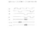
図6にDRAM、SRAM等の汎用メモリをバーンインする際のバーンイン信号の一例を示す。同図に示すように、バーンイン信号は、クロックCLK、行アドレスストローブRAS(以下単にRASという)、列アドレスストローブCAS(以下単にCASという)、ライトイネーブルWEと、データDIN、行アドレスAD(R),列アドレスAD(C)からなり、アドレスはインクリメントされ、メモリの各セルにデータを書き込む処理を行う。
特性モニタ部2は、上記バーンイン信号を被試験対象の各ICに印加し、各IC4bが正常に動作するかを調べ、不良ICのスクリーニングを行う。
【0004】
従来、上記バーンイン槽1内の温度は、作業者が、予めICのスペックの熱抵抗値等からICのチップ内温度が所望の値になるようなバーンイン槽1内の温度を計算し設定していた。
例えば、ICの熱抵抗値が60(°C/W)の場合、ICの内部温度と外部温度の差ΔTjを以下の(1)式で計算し、ICのチップ内温度をTj(例えば125°C)に設定したい場合、以下の(2)式により、ICの周囲温度Ta(即ちバーンイン槽内の温度)を求めて、前記温度制御装置を設定していた。
ΔTj=電源電圧×電源電流×熱抵抗値
=3.6V×100mA×60°C/W
=21.6°C…(1)
Ta=Tj−ΔTj=125−21.6
=103.4°C…(2)
【0005】
【発明が解決しようとする課題】
従来のバーンイン装置は以下の問題点を有していた。
(1) 半導体装置のロット製造のバラツキにより電源電流が変動することがあり、期待するチップ内温度Tjでバーンイン加速試験が行われていない場合があった。
(2) 半導体装置の寿命試験等を行う場合には、通常、温度条件等を実際に使用するときより厳しくし、時間を加速して試験を行っており、この加速係数k(加速時間Tk /バーンイン時間Tbn)は、アレニウスの定理による温度(チップ内温度)と、電圧の積で定めている。なお、ここで加速時間Tk とは、バーンイン時間を、通常の使用条件における半導体装置の使用時間に換算した値である。
したがって、寿命試験等を行うときのバーンイン時間Tbnは、上記加速係数k とバーンイン時間の積が、予め与えられる加速期間Tk になるように定める。
従来においては、チップ内温度が必ずしも期待する値になっていないため、上記加速係数は推定値となり、この推定加速係数を用いてバーンイン時間を定めていた。このため、適切なバーンイン時間によりバーンイン加速試験が行われない場合があった。
(3) 不良ICの解析等を行うため、ICのどの部分が不良であるかを調べることがある。従来のバーンイン装置においては、不良発生時に、ICのどの部分が不良であるか等の詳細な解析をすることができなかった。
本発明は上記従来技術の問題点を解決するためになされたものであって、本発明の目的は、半導体装置のチップ内温度を正確に制御して、最適なバーンイン加速試験を行うことができ、また不良ICの解析を行うことが可能なバーンイン装置を提供することである。
【0006】
【課題を解決するための手段】
図1に示すように、バーンイン槽内に、赤外線センサ等の半導体装置の表面温度や表面温度分布を測定することができる測定手段を設ける。そして、該測定手段により測定された半導体装置の表面温度と、半導体装置のパッケージの熱抵抗値に基づき上記半導体装置の内部温度を求め、該半導体装置の内部温度に基づき、上記バーンイン槽内の温度を制御する。
また、上記のようにして求めた内部温度に基づき加速係数を求め、該加速係数と予め与えられた加速期間からバーンイン時間を定め、該バーンイン時間により上記半導体装置のバーンイン加速試験を行う。
さらに、バーンインを行うことにより、不良半導体が発生したとき、不良が発生した半導体装置の不良アドレスを連続的にアクセスし、前記測定手段により半導体装置の表面温度分布を測定し、上記半導体装置の不良箇所を特定する。
本発明においては、上記のように半導体装置の内部温度を求めて、該内部温度に基づきバーンイン槽内の温度を制御するようにしたので、期待するチップ内温度でバーンイン加速試験を行うことが可能となる。
また、内部温度に基づき加速係数を求め、該加速係数と予め与えられた加速期間からバーンイン時間を定め、該バーンイン時間により上記半導体装置のバーンイン加速試験を行うようにしたので、適切なバーンイン時間によりバーンイン加速試験を行うことができる。
さらに、不良が発生した半導体装置の不良アドレスを連続的にアクセスし、該半導体装置の表面温度分布を測定して、不良半導体装置の不良箇所を特定するようにしたので、不良箇所の検査を行い不良原因等を解析することが可能となる。
【0007】
【発明の実施の形態】
図1は本発明の実施例のバーンイン装置の構成を示す図である。
同図において、1は前記したバーンイン槽であり、バーンイン槽1内にはバーンインカード3が収納され、バーンインカード3に取り付けられたICソケット3aには被検査対象となるIC3bが装着される。なお、同図では、IC3bが一つしか示されていないが、前記図5に示したように、バーンインカード3には複数のICが装着されている。
バーンインカード3に装着された半導体装置3bには、前記したようにICテスタ等からなる特性モニタ部2から、例えば図6に示したようなバーンイン信号を入力され、特性モニタ部2により各ICの電気的特性がモニタされる。
1aはバーンイン槽内の温度を検出する温度センサ、10は前記した温度制御装置であり、温度センサ1aにより検出されたバーンイン槽内の温度が温度制御装置10に送出され、温度制御装置10は、前記したようにバーンイン槽1内に設けられたヒータ等を制御して、バーンイン槽内の温度が所定の値になるように制御する。
【0008】
バーンイン槽3内には、上記温度センサ1aに加え、赤外線センサ制御部11により制御される赤外線センサ1bが設けられている。
赤外線センサ1bは、例えば特開平1−53174号公報に記載されるようなスキャンニング型のセンサであり、上記赤外線センサ制御部11により赤外線センサ1bをスキャンして、バーンイン槽1内に収納された各ICパッケージの表面温度を測定したり、特定のICパッケージの表面温度分布を測定する。赤外線センサ1bとしては、上記公報に開示されるものの外、市販されている各種の赤外線センサを使用することができる。
赤外線センサ1bにより検出されたICの表面温度、表面温度分布等は、赤外線センサ制御部11を介して制御部12に送られる。
【0009】
制御部12は、後述するように上記赤外線センサ1bにより検出されたICの表面温度と、ICの熱抵抗値データからICのチップ内温度を求め、該チップ内温度が所望の値になるように前記温度制御装置10を制御する。また上記チップ内温度に基づきバーンイン時間を定めて、後述するように、タイマー部14にバーンイン時間を設定する。また、上記制御部12は、バーンインコントロール部13を制御して、バーンインを開始/停止させる。
さらに、後述するように、バーンインを行うことにより不良なICが生じたとき、上記制御部12は、特性モニタ部2から上記不良ICのアドレスに連続的にバーンイン信号を送出させ、赤外線センサ1bにより測定された上記不良ICの表面温度分布に基づき、異常発熱箇所を特定する。
【0010】
以下、図1および図2〜図4により、本発明の実施例について説明する。
(1)実施例1
前記したように、従来においては、ICのバラツキにより、期待するチップ内温度Tjでバーンイン加速試験が行われていない場合があった。そこで、本実施例では、バーンイン槽内に収納されたバーンインカードに装着されたICの表面温度からICのチップ内温度を求め、バーンイン槽内を最適な温度に設定する。
図2は本実施例のおける制御部12の処理を示すフローチャートであり図2を参照しながら、本実施例について説明する。
ICが装着されたバーンインカードを図1に示すようにバーンイン槽1内に収納する。制御部12は温度制御装置10によりバーンイン槽1内を所定の温度まで上昇させ、バーンインコントロール部13にバーンイン開始信号を送出する(図2のステップS1)。これにより、特性モニタ部2は、バーンイン信号をバーンイン槽1内のバーンインカード3に装着された各IC3bに送出する。
赤外線センサ1bは、複数のICパッケージの表面温度を検出し、制御部12に送る。制御部12は、上記赤外線センサ1bにより検出されたICパッケージの表面温度の平均値を求める(ステップS2,S3)。そして、上記ICパッケージの表面温度の平均値TsからICのチップ内温度Tjを計算する(ステップS4)。
【0011】
すなわち、ICの内部温度と表面温度の差ΔTjは前記(1)式に示したように、電源電圧×電源電流×ICパッケージの熱抵抗値から求めることができる。
制御部12は、バーンインカードに供給される電源電圧、電源電流と、予め与えられるICパッケージの熱抵抗値から上記ΔTjを求め、上記表面温度の平均値TsとΔTjの和からICのチップ内温度Tjを計算する。
そして、上記ICのチップ内温度Tjが予め定められた値(例えば125°C)になるバーンイン槽1内の温度を求め(ステップS5)、上記温度制御装置10の温度制御部10bに出力する(ステップS6)。
一方、バーンイン槽内の温度は温度センサ1aにより検出され、温度検出部10aから温度制御部10bに送られる。温度制御部12は、上記バーンイン槽1内の温度が上記温度になるように図示しないヒータ等を制御する(ステップS6)。
以上のように、本実施例においては、ICの表面温度を検出して、電源電圧、電源電流と、ICパッケージの熱抵抗値から、ICのチップ内温度を求め、チップ内温度が予め設定された温度になるようにバーンイン槽内の温度を制御しているので、ICの電源電流等にバラツキがあっても、チップ内温度を所望の値にすることができる。このため、所望のチップ内温度でバーンイン加速試験を行うことが可能となる。
【0012】
(2)実施例2
前記したように、半導体装置の寿命試験等を行う場合、バーンイン時間は、加速係数(チップ内温度と電圧の積)と、予め与えられる加速期間に基づき定められる。
上記第1の実施例によれば、ICのチップ内温度を所望の値にすることができるので、上記加速係数を正確に求めることができる。そこで、本実施例においては、上記のようにして求めた加速係数と、予め与えられる加速期間からバーンイン時間を求め、このバーンイン時間によりバーンインを行い、半導体装置の寿命試験を行う。
図3は本実施例における制御部12の処理を示すフローチャートであり図3を参照しながら、本実施例について説明する。
ICが装着されたバーンインカードを図1に示すようにバーンイン槽1内に収納する。制御部12は温度制御装置10によりバーンイン槽1内を所定の温度まで上昇させ、バーンインコントロール部13にバーンイン開始信号を送出する(図3のステップS1)。これにより、特性モニタ部2は、バーンイン信号をバーンイン槽1内のバーンインカード3に装着された各IC3bに送出する。
【0013】
赤外線センサ1bは、複数のICパッケージの表面温度を検出し、制御部12に送る。制御部12は、上記赤外線センサ1bにより検出されたICパッケージの表面温度の平均値を求める(ステップS2,S3)。
ついで、制御部12は、上記ICパッケージの表面温度の平均値Tsから前記したように、ICのチップ内温度Tjを計算する(ステップS4)。
そして、上記ICのチップ内温度Tjが予め定められた値(例えば125°C)になるような、バーンイン槽内の温度を求め、バーンイン槽内の温度を制御する(ステップS5,S6)。
一方、制御部12は、上記チップ内温度TjとICに印加される電圧Vから加速係数を求め(ステップS7)、入力された加速時間Tk と、加速係数kからバーンイン時間Tbnを算出する(ステップS8)。
すなわち、前記したように、加速係数kは、〔温度Tj〕×〔電圧V〕であり、加速時間Tk は、〔加速係数k〕×〔バーンイン時間Tbn〕であるので、バーンイン時間Tbnは、Tk /Tj ×Vにより求めることができる。
制御部12は上記のようにバーンイン時間Tbnを算出し、算出されたバーンイン時間Tbnをタイマ部14に設定する(図3のステップS9)。タイマ部14は、バーンインを開始してから上記設定された時間経過すると、バーンインコントロール部13に停止信号を送出し、バーンイン加速試験を終了させる。
以上のように本実施例においては、ICのチップ内温度に基づき加速係数を定め、該加速係数に基づきバーンイン時間を求めて、バーンイン加速試験を行っているので、適切なバーンイン時間を設定して、バーンイン加速試験を行うことができる。
【0014】
(3)実施例3
不良ICの解析等を行うため、ICのどの部分が不良であるかを調べることがある。本実施例は、上記バーンイン加速試験により不良ICが発生したとき、不良ICの表面温度分布から不良ICの不良箇所を特定し、不良ICを効率的に解析できるようにしたものである
図4は本実施例のおける制御部12の処理を示すフローチャートであり図4を参照しながら、本実施例について説明する。
前記第1、第2の実施例で説明したように、ICが装着されたバーンインカードをバーンイン槽1内に収納し、バーンイン槽1内を所定の温度まで上昇させ、特性モニタ部2から、バーンイン信号をバーンイン槽1内のバーンインカード3に装着された各IC3bに送出し、バーンイン加速試験を行う(図4のステップS1,S2)。
特性モニタ部2は、各ICの電気的特性をモニタし、不良なICが発生したかを調べる(ステップS3,S4)。例えば、ICが汎用メモリの場合、特性モニタ部2は、前記図6に示すバーンイン信号を送出し、各ICの各アドレスに対して、データの書き込み/読み取り処理を行い、各IC3bが正常に動作するかを調べる。そして、不良なICが発生していない場合には、制御部12の、その旨を通知し処理を終了する。
【0015】
一方、不良ICが発生すると、制御部12は特性モニタ部2から不良ICの情報を取得し(ステップS5)、特性モニタ部2に、そのICの不良アドレスに対する連続アクセスを指令する。これにより、特性モニタ部2は、上記不良アドレスに対して連続アクセスを開始する(図4のステップS6)。
一方、制御部12は、赤外線センサ制御部11に対して、上記不良ICのスキャンを指令する。これにより、赤外線センサ1bは、上記不良IC上をスキャンして、その表面温度を検出する。
制御部12は、赤外線センサ1bにより検出された不良ICパッケージの表面温度分布を取得し(ステップS6)、赤外線センサ1bより検出された不良ICパッケージの異常発熱部分から不良ICの不良箇所を特定する(ステップS7)。すなわち、上記のように不良アドレスに対して連続アクセスをすることにより、そのアドレスに対応した部分の温度が他の部分より上昇するので、ICパッケージの表面温度分布により、ICパッケージ上における不良アドレスの位置を特定することができる。
なお、上記不良ICの表面温度分布をモニタ上に表示し、モニタ画面を作業者が観察して、不良箇所を特定するようにしてもよい。
以上のように、本実施例においては、不良ICが発生したとき、その不良アドレスに連続的にアクセスし、赤外線センサ1bにより、不良ICパッケージ表面温度分布を検出するようにしたので、不良ICの不良箇所を特定することができる。このため、例えば、不良ICを開いて、不良ICの内部の不良箇所を検査することが可能となり、不良原因の解析等を行うことができる。
【0016】
【発明の効果】
以上説明したように、本発明においては、以下の効果を得ることができる。
(1)半導体装置の内部温度を求めて、該内部温度に基づきバーンイン槽内の温度を制御するようにしたので、最適なバーンイン温度を設定することができる。(2)上記内部温度に基づき加速係数を求め、該加速係数と予め与えられた加速期間からバーンイン時間を定め、該バーンイン時間により上記半導体装置のバーンイン加速試験を行うようにしたので、適切なバーンイン時間によりバーンイン加速試験を行うことができる。
(3)不良が発生した半導体装置の不良アドレスを連続的にアクセスし、該半導体装置の表面温度分布を測定して、不良半導体装置の不良箇所を特定するようにしたので、不良箇所の検査を行い不良原因等を解析することが可能となる。
【図面の簡単な説明】
【図1】本発明の実施例のバーンイン装置の構成を示す図である。
【図2】本発明の第1の実施例の処理を示すフローチャートである。
【図3】本発明の第2の実施例の処理を示すフローチャートである。
【図4】本発明の第3の実施例の処理を示すフローチャートである。
【図5】バーンイン装置とバーンインカードの構成例を示す図である。
【図6】汎用メモリをバーンインする際のバーンイン信号の一例を示す図である。
【符号の説明】
1 バーンイン槽
1a 温度センサ
1b 赤外線センサ
2 特性モニタ部
3 バーンインカード
3a ICソケット
3b 半導体装置
10 温度制御装置
11 赤外線センサ制御部
12 制御部
14 タイマー部
13 バーンインコントロール部[0001]
BACKGROUND OF THE INVENTION
The present invention relates to a burn-in apparatus for screening defective semiconductors, and more particularly to a burn-in apparatus capable of performing burn-in by setting an optimal burn-in temperature.
[0002]
[Prior art]
Conventionally, when receiving a semiconductor device, the semiconductor device is stored in a burn-in tank, a burn-in signal is input from a signal generator to the semiconductor device, and dynamic burn-in is performed to screen defective products. Yes.
FIG. 5A shows a schematic configuration of the burn-in apparatus, and FIG. 5B shows a configuration example of the burn-in card.
For example, as shown in FIG. 1A, the burn-in apparatus includes a burn-in tank 1, a
A semiconductor device such as an LSI to be tested is mounted in an IC socket 3a provided in the burn-in
The burn-in
[0003]
A temperature sensor 1 a for measuring the temperature in the tank is provided in the burn-in
The inside of the burn-in tank 1 is maintained at a predetermined temperature by the temperature control device 10, and a burn-in signal is input from the
FIG. 6 shows an example of a burn-in signal when a general-purpose memory such as DRAM or SRAM is burned in. As shown in the figure, the burn-in signal includes a clock CLK, a row address strobe RAS (hereinafter simply referred to as RAS), a column address strobe CAS (hereinafter simply referred to as CAS), a write enable WE, data DIN, and a row address AD (R). , Column address AD (C), the address is incremented, and data is written to each cell of the memory.
The
[0004]
Conventionally, the temperature in the burn-in tank 1 is calculated and set in advance by an operator so that the temperature in the chip of the IC becomes a desired value based on the thermal resistance value of the IC specifications. It was.
For example, when the thermal resistance value of the IC is 60 (° C / W), the difference ΔTj between the internal temperature and the external temperature of the IC is calculated by the following equation (1), and the internal temperature of the IC is calculated as Tj (for example, 125 ° When it is desired to set to C), the ambient temperature Ta of the IC (that is, the temperature in the burn-in tank) is obtained by the following equation (2), and the temperature control device is set.
ΔTj = power supply voltage × power supply current × thermal resistance = 3.6 V × 100 mA × 60 ° C / W
= 21.6 ° C (1)
Ta = Tj−ΔTj = 15-26-21.6
= 103.4 ° C (2)
[0005]
[Problems to be solved by the invention]
The conventional burn-in apparatus has the following problems.
(1) The power supply current may fluctuate due to variations in manufacturing lots of semiconductor devices, and the burn-in acceleration test may not be performed at the expected in-chip temperature Tj.
(2) When conducting a life test or the like of a semiconductor device, the temperature condition is usually made stricter than when actually used, and the test is performed by accelerating the time. This acceleration factor k (acceleration time Tk / The burn-in time Tbn) is determined by the product of the temperature (in-chip temperature) according to the Arrhenius theorem and the voltage. Here, the acceleration time Tk is a value obtained by converting the burn-in time into the use time of the semiconductor device under normal use conditions.
Therefore, the burn-in time Tbn when performing a life test or the like is determined so that the product of the acceleration coefficient k and the burn-in time becomes an acceleration period Tk given in advance.
Conventionally, since the temperature inside the chip is not necessarily an expected value, the acceleration coefficient is an estimated value, and the burn-in time is determined using the estimated acceleration coefficient. For this reason, the burn-in acceleration test may not be performed due to an appropriate burn-in time.
(3) In order to analyze a defective IC, etc., it may be checked which part of the IC is defective. In the conventional burn-in apparatus, when a defect occurs, detailed analysis such as which part of the IC is defective cannot be performed.
The present invention has been made to solve the above-described problems of the prior art, and an object of the present invention is to perform an optimal burn-in acceleration test by accurately controlling the temperature in a chip of a semiconductor device. Another object of the present invention is to provide a burn-in device capable of analyzing a defective IC.
[0006]
[Means for Solving the Problems]
As shown in FIG. 1, measuring means capable of measuring the surface temperature and surface temperature distribution of a semiconductor device such as an infrared sensor is provided in the burn-in tank. Then, the internal temperature of the semiconductor device is determined based on the surface temperature of the semiconductor device measured by the measuring means and the thermal resistance value of the package of the semiconductor device, and the temperature in the burn-in tank is determined based on the internal temperature of the semiconductor device. To control.
Further, an acceleration coefficient is obtained based on the internal temperature obtained as described above, a burn-in time is determined from the acceleration coefficient and a predetermined acceleration period, and a burn-in acceleration test of the semiconductor device is performed based on the burn-in time.
Further, by performing burn-in, when a defective semiconductor occurs, the defective address of the semiconductor device in which the defect has occurred is continuously accessed, the surface temperature distribution of the semiconductor device is measured by the measuring means, and the defect of the semiconductor device is detected. Identify the location.
In the present invention, the internal temperature of the semiconductor device is obtained as described above, and the temperature in the burn-in tank is controlled based on the internal temperature, so that it is possible to perform a burn-in acceleration test at the expected internal temperature. It becomes.
Further, the acceleration coefficient is obtained based on the internal temperature, the burn-in time is determined from the acceleration coefficient and a predetermined acceleration period, and the burn-in acceleration test of the semiconductor device is performed by the burn-in time. Burn-in acceleration test can be performed.
In addition, the defective address of the semiconductor device in which the defect has occurred is continuously accessed, and the surface temperature distribution of the semiconductor device is measured to identify the defective portion of the defective semiconductor device. It becomes possible to analyze the cause of the defect.
[0007]
DETAILED DESCRIPTION OF THE INVENTION
FIG. 1 is a diagram showing the configuration of a burn-in apparatus according to an embodiment of the present invention.
In the figure, reference numeral 1 denotes the above-described burn-in tank. A burn-in
For example, a burn-in signal as shown in FIG. 6 is input to the semiconductor device 3b mounted on the burn-in
1a is a temperature sensor that detects the temperature in the burn-in tank, 10 is the above-described temperature control device, the temperature in the burn-in tank detected by the temperature sensor 1a is sent to the temperature control device 10, and the temperature control device 10 As described above, the heater or the like provided in the burn-in tank 1 is controlled so that the temperature in the burn-in tank becomes a predetermined value.
[0008]
In the burn-in
The infrared sensor 1b is a scanning type sensor as described in, for example, Japanese Patent Laid-Open No. 1-53174. The infrared
The IC surface temperature, surface temperature distribution, and the like detected by the infrared sensor 1 b are sent to the
[0009]
As will be described later, the
Further, as described later, when a defective IC is generated by performing burn-in, the
[0010]
Hereinafter, an embodiment of the present invention will be described with reference to FIGS. 1 and 2 to 4.
(1) Example 1
As described above, conventionally, the burn-in acceleration test may not be performed at the expected in-chip temperature Tj due to IC variation. Therefore, in this embodiment, the temperature inside the IC chip is obtained from the surface temperature of the IC mounted on the burn-in card housed in the burn-in tank, and the inside of the burn-in tank is set to an optimum temperature.
FIG. 2 is a flowchart showing the processing of the
The burn-in card on which the IC is mounted is stored in the burn-in tank 1 as shown in FIG. The
The infrared sensor 1 b detects surface temperatures of a plurality of IC packages and sends them to the
[0011]
That is, the difference ΔTj between the internal temperature and the surface temperature of the IC can be obtained from the power supply voltage × the power supply current × the thermal resistance value of the IC package, as shown in the equation (1).
The
Then, the temperature in the burn-in tank 1 at which the in-chip temperature Tj of the IC becomes a predetermined value (for example, 125 ° C.) is obtained (step S5), and is output to the
On the other hand, the temperature in the burn-in tank is detected by the temperature sensor 1a and sent from the
As described above, in this embodiment, the IC surface temperature is detected, the IC internal temperature is obtained from the power supply voltage, the power supply current, and the thermal resistance value of the IC package, and the internal temperature is preset. Since the temperature in the burn-in tank is controlled so as to be the same temperature, even if there is a variation in the power supply current of the IC, the temperature in the chip can be set to a desired value. For this reason, it becomes possible to perform a burn-in acceleration test at a desired in-chip temperature.
[0012]
(2) Example 2
As described above, when performing a life test or the like of a semiconductor device, the burn-in time is determined based on an acceleration coefficient (product of chip temperature and voltage) and an acceleration period given in advance.
According to the first embodiment, since the IC internal temperature can be set to a desired value, the acceleration coefficient can be accurately obtained. Therefore, in this embodiment, the burn-in time is obtained from the acceleration coefficient obtained as described above and an acceleration period given in advance, and burn-in is performed using this burn-in time, and the life test of the semiconductor device is performed.
FIG. 3 is a flowchart showing the processing of the
The burn-in card on which the IC is mounted is stored in the burn-in tank 1 as shown in FIG. The
[0013]
The infrared sensor 1 b detects surface temperatures of a plurality of IC packages and sends them to the
Next, as described above, the
Then, the temperature in the burn-in tank is determined such that the temperature in the chip Tj of the IC becomes a predetermined value (for example, 125 ° C.), and the temperature in the burn-in tank is controlled (steps S5 and S6).
On the other hand, the
That is, as described above, since the acceleration coefficient k is [temperature Tj] × [voltage V] and the acceleration time Tk is [acceleration coefficient k] × [burn-in time Tbn], the burn-in time Tbn is Tk. / Tj × V.
The
As described above, in this embodiment, the acceleration coefficient is determined based on the temperature inside the chip of the IC, the burn-in time is obtained based on the acceleration coefficient, and the burn-in acceleration test is performed. Therefore, an appropriate burn-in time is set. A burn-in acceleration test can be performed.
[0014]
(3) Example 3
In order to analyze a defective IC or the like, it may be checked which part of the IC is defective. In this embodiment, when a defective IC is generated by the burn-in acceleration test, the defective IC is identified from the surface temperature distribution of the defective IC, and the defective IC can be efficiently analyzed. It is a flowchart which shows the process of the
As described in the first and second embodiments, the burn-in card with the IC mounted therein is accommodated in the burn-in tank 1 and the inside of the burn-in tank 1 is raised to a predetermined temperature. A signal is sent to each IC 3b mounted on the burn-in
The
[0015]
On the other hand, when a defective IC occurs, the
On the other hand, the
The
The surface temperature distribution of the defective IC may be displayed on a monitor, and the operator may observe the monitor screen to identify the defective portion.
As described above, in this embodiment, when a defective IC occurs, the defective address is continuously accessed and the surface temperature distribution of the defective IC package is detected by the infrared sensor 1b. A defective part can be specified. For this reason, for example, it is possible to open a defective IC to inspect a defective portion inside the defective IC, and to analyze the cause of the defect.
[0016]
【The invention's effect】
As described above, the following effects can be obtained in the present invention.
(1) Since the internal temperature of the semiconductor device is obtained and the temperature in the burn-in tank is controlled based on the internal temperature, the optimum burn-in temperature can be set. (2) An acceleration coefficient is obtained based on the internal temperature, a burn-in time is determined from the acceleration coefficient and a predetermined acceleration period, and a burn-in acceleration test of the semiconductor device is performed based on the burn-in time. A burn-in acceleration test can be performed according to time.
(3) Since the defective address of the semiconductor device in which the defect has occurred is continuously accessed and the surface temperature distribution of the semiconductor device is measured to identify the defective portion of the defective semiconductor device, the defective portion is inspected. It is possible to analyze the cause of failure.
[Brief description of the drawings]
FIG. 1 is a diagram showing a configuration of a burn-in apparatus according to an embodiment of the present invention.
FIG. 2 is a flowchart showing processing of the first exemplary embodiment of the present invention.
FIG. 3 is a flowchart showing processing of a second embodiment of the present invention.
FIG. 4 is a flowchart showing processing of a third embodiment of the present invention.
FIG. 5 is a diagram showing a configuration example of a burn-in device and a burn-in card.
FIG. 6 is a diagram illustrating an example of a burn-in signal when a general-purpose memory is burned-in.
[Explanation of symbols]
DESCRIPTION OF SYMBOLS 1 Burn-in tank 1a Temperature sensor
Claims (1)
Translated fromJapanese上記半導体装置の表面温度分布を測定する測定手段と、
被試験対象の半導体装置のバーンイン試験中の電気的特性をモニタする特性モニタ部と、
バーンイン装置を制御する制御手段を備え、
前記特性モニタ部によって不良半導体素子を発見した場合、上記制御手段に、上記特性モニタ部を制御して上記不良半導体素子の不良アドレスに対して連続的にアクセスし、そのアドレスに対応した部分の温度を他の部分より上昇させる手順と、
前記測定手段を制御して測定された上記不良半導体素子の表面温度分布を測定する手順と、上記表面温度分布を基に上記不良半導体素子の不良箇所を特定する手順とを実行させる
ことを特徴とするダイナミック・バーンイン装置。A dynamic burn-in apparatus for inputting a burn-in signal to a semiconductor device having at least one semiconductor element to be tested stored in a burn-in tank and performing burn-in of the semiconductor device,
Measuring means for measuring the surface temperature distribution of the semiconductor device;
A characteristic monitor for monitoring the electrical characteristics of the semiconductor device under test during the burn-in test;
Comprising control means for controlling the burn-in device;
When a defective semiconductor element is found by the characteristic monitor unit, the control unit controls the characteristic monitor unit to continuously access the defective address of the defective semiconductor element, andthe temperature of the portion corresponding to the address The procedure toraise the other than other parts ,
A step of measuring the surface temperature distribution of the defective semiconductor element measured by controlling the measuring means, and a step of identifying a defective portion of the defective semiconductor element based on the surface temperature distribution. Dynamic burn-in device.
Priority Applications (2)
| Application Number | Priority Date | Filing Date | Title |
|---|---|---|---|
| JP2001386153AJP4148677B2 (en) | 2001-12-19 | 2001-12-19 | Dynamic burn-in equipment |
| US10/869,966US7023229B2 (en) | 2001-12-19 | 2004-06-18 | Dynamic burn-in equipment |
Applications Claiming Priority (1)
| Application Number | Priority Date | Filing Date | Title |
|---|---|---|---|
| JP2001386153AJP4148677B2 (en) | 2001-12-19 | 2001-12-19 | Dynamic burn-in equipment |
Publications (2)
| Publication Number | Publication Date |
|---|---|
| JP2003185712A JP2003185712A (en) | 2003-07-03 |
| JP4148677B2true JP4148677B2 (en) | 2008-09-10 |
Family
ID=27595383
Family Applications (1)
| Application Number | Title | Priority Date | Filing Date |
|---|---|---|---|
| JP2001386153AExpired - Fee RelatedJP4148677B2 (en) | 2001-12-19 | 2001-12-19 | Dynamic burn-in equipment |
Country Status (2)
| Country | Link |
|---|---|
| US (1) | US7023229B2 (en) |
| JP (1) | JP4148677B2 (en) |
Families Citing this family (45)
| Publication number | Priority date | Publication date | Assignee | Title |
|---|---|---|---|---|
| US5345170A (en) | 1992-06-11 | 1994-09-06 | Cascade Microtech, Inc. | Wafer probe station having integrated guarding, Kelvin connection and shielding systems |
| US6380751B2 (en) | 1992-06-11 | 2002-04-30 | Cascade Microtech, Inc. | Wafer probe station having environment control enclosure |
| US5561377A (en) | 1995-04-14 | 1996-10-01 | Cascade Microtech, Inc. | System for evaluating probing networks |
| US6002263A (en) | 1997-06-06 | 1999-12-14 | Cascade Microtech, Inc. | Probe station having inner and outer shielding |
| US6445202B1 (en) | 1999-06-30 | 2002-09-03 | Cascade Microtech, Inc. | Probe station thermal chuck with shielding for capacitive current |
| US6838890B2 (en)* | 2000-02-25 | 2005-01-04 | Cascade Microtech, Inc. | Membrane probing system |
| US6914423B2 (en) | 2000-09-05 | 2005-07-05 | Cascade Microtech, Inc. | Probe station |
| US6965226B2 (en) | 2000-09-05 | 2005-11-15 | Cascade Microtech, Inc. | Chuck for holding a device under test |
| WO2003020467A1 (en) | 2001-08-31 | 2003-03-13 | Cascade Microtech, Inc. | Optical testing device |
| US6777964B2 (en) | 2002-01-25 | 2004-08-17 | Cascade Microtech, Inc. | Probe station |
| US6951846B2 (en)* | 2002-03-07 | 2005-10-04 | The United States Of America As Represented By The Secretary Of The Army | Artemisinins with improved stability and bioavailability for therapeutic drug development and application |
| US6847219B1 (en) | 2002-11-08 | 2005-01-25 | Cascade Microtech, Inc. | Probe station with low noise characteristics |
| US7250779B2 (en) | 2002-11-25 | 2007-07-31 | Cascade Microtech, Inc. | Probe station with low inductance path |
| US6861856B2 (en)* | 2002-12-13 | 2005-03-01 | Cascade Microtech, Inc. | Guarded tub enclosure |
| US7221172B2 (en) | 2003-05-06 | 2007-05-22 | Cascade Microtech, Inc. | Switched suspended conductor and connection |
| US7492172B2 (en) | 2003-05-23 | 2009-02-17 | Cascade Microtech, Inc. | Chuck for holding a device under test |
| US7265561B2 (en)* | 2003-09-30 | 2007-09-04 | International Business Machines Corporation | Device burn in utilizing voltage control |
| US7250626B2 (en) | 2003-10-22 | 2007-07-31 | Cascade Microtech, Inc. | Probe testing structure |
| US7187188B2 (en) | 2003-12-24 | 2007-03-06 | Cascade Microtech, Inc. | Chuck with integrated wafer support |
| US7394271B2 (en)* | 2004-02-27 | 2008-07-01 | Wells-Cti, Llc | Temperature sensing and prediction in IC sockets |
| JP4490168B2 (en)* | 2004-05-21 | 2010-06-23 | 富士通株式会社 | Defective device analysis method |
| WO2005121824A2 (en) | 2004-06-07 | 2005-12-22 | Cascade Microtech, Inc. | Thermal optical chuck |
| US7330041B2 (en)* | 2004-06-14 | 2008-02-12 | Cascade Microtech, Inc. | Localizing a temperature of a device for testing |
| US7656172B2 (en) | 2005-01-31 | 2010-02-02 | Cascade Microtech, Inc. | System for testing semiconductors |
| US7535247B2 (en) | 2005-01-31 | 2009-05-19 | Cascade Microtech, Inc. | Interface for testing semiconductors |
| EP1866656A2 (en)* | 2005-03-08 | 2007-12-19 | Wells-CTI, Llc. | Temperature sensing and prediction in ic sockets |
| US20070294047A1 (en)* | 2005-06-11 | 2007-12-20 | Leonard Hayden | Calibration system |
| US20070030019A1 (en)* | 2005-08-04 | 2007-02-08 | Micron Technology, Inc. | Power sink for IC temperature control |
| US8025097B2 (en) | 2006-05-18 | 2011-09-27 | Centipede Systems, Inc. | Method and apparatus for setting and controlling temperature |
| US7921803B2 (en)* | 2007-09-21 | 2011-04-12 | Applied Materials, Inc. | Chamber components with increased pyrometry visibility |
| US8319503B2 (en) | 2008-11-24 | 2012-11-27 | Cascade Microtech, Inc. | Test apparatus for measuring a characteristic of a device under test |
| US8008934B2 (en)* | 2009-06-10 | 2011-08-30 | Freescale Semiconductor, Inc. | Burn-in system for electronic devices |
| US9152517B2 (en) | 2011-04-21 | 2015-10-06 | International Business Machines Corporation | Programmable active thermal control |
| CN103185855B (en)* | 2011-12-27 | 2016-02-10 | 英业达股份有限公司 | Test Equipment |
| KR102245131B1 (en) | 2014-10-23 | 2021-04-28 | 삼성전자 주식회사 | Apparatus and method using programmable reliability aging timer |
| US9841459B2 (en)* | 2015-10-26 | 2017-12-12 | Test21 Taiwan Co., Ltd. | Device and method for controlling IC temperature |
| DE102016206339B4 (en)* | 2015-12-23 | 2019-02-07 | Brose Fahrzeugteile GmbH & Co. Kommanditgesellschaft, Würzburg | Electronic module of an accessory of a motor vehicle |
| JP6880671B2 (en)* | 2016-11-22 | 2021-06-02 | 株式会社リコー | Dynamic burn-in device and control device for it |
| KR101877667B1 (en)* | 2017-02-28 | 2018-07-11 | 세메스 주식회사 | Method of testing semiconductor packages |
| US10514416B2 (en)* | 2017-09-29 | 2019-12-24 | Advantest Corporation | Electronic component handling apparatus and electronic component testing apparatus |
| CN109297891A (en)* | 2018-10-24 | 2019-02-01 | 中国电器科学研究院有限公司 | A kind of arid and hot environment outdoor aging accelerated test method of high molecular material |
| CN111124004B (en)* | 2019-12-11 | 2021-11-23 | 苏州通富超威半导体有限公司 | Test board, test frame, temperature difference control system and method for high-acceleration stress test |
| JP7427996B2 (en)* | 2020-02-13 | 2024-02-06 | 富士電機株式会社 | Testing method for semiconductor devices |
| KR102854378B1 (en)* | 2020-08-20 | 2025-09-02 | 삼성전자주식회사 | Semiconductor package test device and method for the same |
| KR102495025B1 (en)* | 2022-03-18 | 2023-02-06 | 주식회사디아이 | Temperature uniformity monitoring device of burn-in chamber |
Family Cites Families (10)
| Publication number | Priority date | Publication date | Assignee | Title |
|---|---|---|---|---|
| JPS63115074A (en) | 1986-10-31 | 1988-05-19 | Mitsubishi Electric Corp | Semiconductor high-temperature acceleration testing device |
| JPH0758311B2 (en) | 1987-08-22 | 1995-06-21 | 東京エレクトロン株式会社 | Semiconductor device inspection method |
| CA2073886A1 (en)* | 1991-07-19 | 1993-01-20 | Tatsuya Hashinaga | Burn-in apparatus and method |
| JP2962129B2 (en)* | 1993-12-29 | 1999-10-12 | 日本電気株式会社 | Semiconductor test equipment |
| JPH0876857A (en) | 1994-09-02 | 1996-03-22 | Hitachi Electron Eng Co Ltd | Temperature control method for constant temperature bath of IC handler |
| JP2000097990A (en) | 1998-09-24 | 2000-04-07 | Mitsubishi Electric Corp | Semiconductor device burn-in test equipment |
| JP2000206176A (en)* | 1999-01-07 | 2000-07-28 | Nippon Scientific Co Ltd | Burn-in device |
| JP3054141B1 (en)* | 1999-03-31 | 2000-06-19 | エム・シー・エレクトロニクス株式会社 | IC device temperature control device and inspection device |
| JP2001272434A (en) | 2000-03-24 | 2001-10-05 | Matsushita Electric Ind Co Ltd | Semiconductor element test method and test apparatus |
| JP2001324390A (en) | 2000-05-17 | 2001-11-22 | Denso Corp | Thermal type infrared image sensor |
- 2001
- 2001-12-19JPJP2001386153Apatent/JP4148677B2/ennot_activeExpired - Fee Related
- 2004
- 2004-06-18USUS10/869,966patent/US7023229B2/ennot_activeExpired - Fee Related
Also Published As
| Publication number | Publication date |
|---|---|
| US7023229B2 (en) | 2006-04-04 |
| JP2003185712A (en) | 2003-07-03 |
| US20040232933A1 (en) | 2004-11-25 |
Similar Documents
| Publication | Publication Date | Title |
|---|---|---|
| JP4148677B2 (en) | Dynamic burn-in equipment | |
| US5032727A (en) | Product defect detection using thermal ratio analysis | |
| US7714599B2 (en) | Integrated circuit burn-in test system and associated methods | |
| US6788093B2 (en) | Methodology and apparatus using real-time optical signal for wafer-level device dielectrical reliability studies | |
| US6414508B1 (en) | Methods for predicting reliability of semiconductor devices using voltage stressing | |
| US6593761B1 (en) | Test handler for semiconductor device | |
| US20250180637A1 (en) | Wafer test system and operating method thereof | |
| JPH11260872A (en) | Screening prober | |
| JP2008204975A (en) | Semiconductor device inspection apparatus and inspection method using the same | |
| JP6157270B2 (en) | Probe apparatus and probe method | |
| US7617427B2 (en) | Method and apparatus for detecting defects in integrated circuit die from stimulation of statistical outlier signatures | |
| JP2011215007A (en) | Testing device and testing method | |
| US8829898B1 (en) | Method and apparatus for testing | |
| JP2008175540A (en) | Method and system for inspecting thin-film capacitor | |
| Prarop et al. | The Utilization of Seebeck effect for Edge Seal Die Failure Analysis | |
| JP2022096153A (en) | Electronic device inspection equipment and inspection method | |
| US6978407B2 (en) | Method and architecture for detecting random and systematic transistor degradation for transistor reliability evaluation in high-density memory | |
| JP2004184417A (en) | System and method for tolerance evaluation of chip and improvement in yield | |
| JP2008124049A (en) | Inspection method of semiconductor chip | |
| KR20080002496A (en) | Semiconductor device test system | |
| JP4062424B2 (en) | Memory test system and memory test method | |
| JP2002040094A (en) | Testing method for semiconductor device and testing device for semiconductor device | |
| JP2984155B2 (en) | Wafer IC chip inspection method | |
| JPH08334545A (en) | Semiconductor device measuring device | |
| JPH03165047A (en) | Burn-in apparatus |
Legal Events
| Date | Code | Title | Description |
|---|---|---|---|
| A621 | Written request for application examination | Free format text:JAPANESE INTERMEDIATE CODE: A621 Effective date:20040907 | |
| A131 | Notification of reasons for refusal | Free format text:JAPANESE INTERMEDIATE CODE: A131 Effective date:20070904 | |
| A521 | Request for written amendment filed | Free format text:JAPANESE INTERMEDIATE CODE: A523 Effective date:20071031 | |
| A131 | Notification of reasons for refusal | Free format text:JAPANESE INTERMEDIATE CODE: A131 Effective date:20080408 | |
| A521 | Request for written amendment filed | Free format text:JAPANESE INTERMEDIATE CODE: A523 Effective date:20080530 | |
| TRDD | Decision of grant or rejection written | ||
| A01 | Written decision to grant a patent or to grant a registration (utility model) | Free format text:JAPANESE INTERMEDIATE CODE: A01 Effective date:20080624 | |
| A01 | Written decision to grant a patent or to grant a registration (utility model) | Free format text:JAPANESE INTERMEDIATE CODE: A01 | |
| A61 | First payment of annual fees (during grant procedure) | Free format text:JAPANESE INTERMEDIATE CODE: A61 Effective date:20080624 | |
| FPAY | Renewal fee payment (event date is renewal date of database) | Free format text:PAYMENT UNTIL: 20110704 Year of fee payment:3 | |
| R150 | Certificate of patent or registration of utility model | Free format text:JAPANESE INTERMEDIATE CODE: R150 | |
| FPAY | Renewal fee payment (event date is renewal date of database) | Free format text:PAYMENT UNTIL: 20110704 Year of fee payment:3 | |
| FPAY | Renewal fee payment (event date is renewal date of database) | Free format text:PAYMENT UNTIL: 20120704 Year of fee payment:4 | |
| FPAY | Renewal fee payment (event date is renewal date of database) | Free format text:PAYMENT UNTIL: 20120704 Year of fee payment:4 | |
| FPAY | Renewal fee payment (event date is renewal date of database) | Free format text:PAYMENT UNTIL: 20130704 Year of fee payment:5 | |
| LAPS | Cancellation because of no payment of annual fees |