JP4146613B2 - Semiconductor device - Google Patents
Semiconductor deviceDownload PDFInfo
- Publication number
- JP4146613B2 JP4146613B2JP2000376296AJP2000376296AJP4146613B2JP 4146613 B2JP4146613 B2JP 4146613B2JP 2000376296 AJP2000376296 AJP 2000376296AJP 2000376296 AJP2000376296 AJP 2000376296AJP 4146613 B2JP4146613 B2JP 4146613B2
- Authority
- JP
- Japan
- Prior art keywords
- power supply
- signal output
- region
- group
- drive signals
- Prior art date
- Legal status (The legal status is an assumption and is not a legal conclusion. Google has not performed a legal analysis and makes no representation as to the accuracy of the status listed.)
- Expired - Fee Related
Links
- 239000004065semiconductorSubstances0.000titleclaimsdescription23
- 239000000758substrateSubstances0.000claimsdescription33
- 239000004973liquid crystal related substanceSubstances0.000claimsdescription6
- XUIMIQQOPSSXEZ-UHFFFAOYSA-NSiliconChemical compound[Si]XUIMIQQOPSSXEZ-UHFFFAOYSA-N0.000description20
- 229910052710siliconInorganic materials0.000description20
- 239000010703siliconSubstances0.000description20
- 239000010931goldSubstances0.000description12
- 238000010586diagramMethods0.000description8
- 239000011521glassSubstances0.000description7
- PCHJSUWPFVWCPO-UHFFFAOYSA-NgoldChemical compound[Au]PCHJSUWPFVWCPO-UHFFFAOYSA-N0.000description6
- 229910052737goldInorganic materials0.000description6
- 102100024452DNA-directed RNA polymerase III subunit RPC1Human genes0.000description4
- 101000689002Homo sapiens DNA-directed RNA polymerase III subunit RPC1Proteins0.000description4
Images


Classifications
- G—PHYSICS
- G09—EDUCATION; CRYPTOGRAPHY; DISPLAY; ADVERTISING; SEALS
- G09G—ARRANGEMENTS OR CIRCUITS FOR CONTROL OF INDICATING DEVICES USING STATIC MEANS TO PRESENT VARIABLE INFORMATION
- G09G3/00—Control arrangements or circuits, of interest only in connection with visual indicators other than cathode-ray tubes
- G09G3/20—Control arrangements or circuits, of interest only in connection with visual indicators other than cathode-ray tubes for presentation of an assembly of a number of characters, e.g. a page, by composing the assembly by combination of individual elements arranged in a matrix no fixed position being assigned to or needed to be assigned to the individual characters or partial characters
- G09G3/34—Control arrangements or circuits, of interest only in connection with visual indicators other than cathode-ray tubes for presentation of an assembly of a number of characters, e.g. a page, by composing the assembly by combination of individual elements arranged in a matrix no fixed position being assigned to or needed to be assigned to the individual characters or partial characters by control of light from an independent source
- G09G3/36—Control arrangements or circuits, of interest only in connection with visual indicators other than cathode-ray tubes for presentation of an assembly of a number of characters, e.g. a page, by composing the assembly by combination of individual elements arranged in a matrix no fixed position being assigned to or needed to be assigned to the individual characters or partial characters by control of light from an independent source using liquid crystals
- G09G3/3611—Control of matrices with row and column drivers
- G—PHYSICS
- G09—EDUCATION; CRYPTOGRAPHY; DISPLAY; ADVERTISING; SEALS
- G09G—ARRANGEMENTS OR CIRCUITS FOR CONTROL OF INDICATING DEVICES USING STATIC MEANS TO PRESENT VARIABLE INFORMATION
- G09G2330/00—Aspects of power supply; Aspects of display protection and defect management
- G09G2330/02—Details of power systems and of start or stop of display operation
Landscapes
- Engineering & Computer Science (AREA)
- Chemical & Material Sciences (AREA)
- Crystallography & Structural Chemistry (AREA)
- Physics & Mathematics (AREA)
- Computer Hardware Design (AREA)
- General Physics & Mathematics (AREA)
- Theoretical Computer Science (AREA)
- Liquid Crystal (AREA)
- Semiconductor Integrated Circuits (AREA)
Description
Translated fromJapanese【0001】
【発明の属する技術分野】
本発明は、LCDパネル等の表示デバイスを駆動する半導体装置(ドライバIC)に関する。
【0002】
【従来の技術】
LCDパネルを駆動する従来のドライバICについて図3〜図4を参照しながら説明する。
【0003】
図3は、従来の半導体装置を用いたLCDモジュールを示す図である。図3に示すように、このLCDモジュール40は、ドライバIC31と、LCDパネル20と、ガラス基板41とを含んでいる。即ち、ガラス基板41上にドライバIC31とLCDパネル20とが実装され、LCDモジュール40を構成している。
【0004】
LCDパネル20は、セグメント方向において複数の領域101、102、・・・を有し、コモン方向においても複数の領域301、302、・・・を有している。ここで、セグメント方向の1つの領域とコモン方向の1つの領域を特定することにより、1つの画素(ドット)が特定される。一例としては、LCDパネル20が、セグメント方向において160個の領域を有し、コモン方向においても160個の領域を有する。この場合には、LCDパネル20は、160×160の画素を有することになる。
【0005】
ドライバIC31は1つの方向に長い形状を有しており、その実装面の長手方向の一辺(図中上方の辺)の中央部に沿ってセグメント信号を出力するための金(Au)バンプのセグメント信号出力端子S201〜S360が形成されている。また、ドライバIC31の実装面の長手方向の一辺(図中上方の辺)の上記中央部の両側の部分に沿って、コモン信号を出力するための金(Au)バンプのコモン信号出力端子C201〜C280及びC281〜C360が形成されている。更に、ドライバIC31の実装面の長手方向の他辺(図中下方の辺)に沿って、金(Au)バンプの入力端子Q1〜Qnが形成されている。
【0006】
ガラス基板41上において、透明な配線LS201〜LS360及びLC201〜LC360が形成されている。LCDパネル20の領域101〜260には、配線LS201〜LS360によって、ドライバIC31のセグメント信号出力端子S201〜S360がそれぞれ接続されている。また、LCDパネル20の領域301〜380には、配線LC201〜LC280によって、ドライバIC31のコモン信号出力端子C201〜C280がそれぞれ接続され、LCDパネル20の領域381〜460には、配線LC360〜LC281によって、ドライバIC31のコモン信号出力端子C360〜C281がそれぞれ接続されている。
【0007】
図4は、ドライバIC31の内部構成を示す図である。図4において、ドライバIC31は、パッケージ32と、パッケージ32に封入されたシリコン基板33とを含んでいる。
【0008】
シリコン基板33上の長手方向の一辺(図中上方の辺)に沿って、セグメント信号出力部34が形成されている。また、シリコン基板33上の短手方向の両辺に沿って、コモン信号出力部35〜36がそれぞれ形成されている。更に、シリコン基板33上の長手方向の他辺(図中下方の辺)に沿って、電源部37、制御部38、及び、RAM39が、それぞれ形成されている。セグメント信号出力部34、コモン信号出力部35〜36、電源部37、制御部38、及び、RAM39は、配線(図示せず)によって相互に接続されている。
【0009】
セグメント信号出力部34は、セグメント信号出力端子S201〜S360に接続されており、これらのセグメント信号出力端子からセグメント信号を出力する。
コモン信号出力部35は、コモン信号出力端子C201〜C280に接続されており、これらのコモン信号出力端子からコモン信号を出力する。コモン信号出力部36は、コモン信号出力端子C281〜C360に接続されており、これらのコモン信号出力端子C281〜C360からコモン信号を出力する。
【0010】
電源部37、制御部38、及び、RAM39は、入力端子Q1〜Qnに接続されており、これらの入力端子から電源電位、制御信号、画像データ等の入力を行う。
電源部37は、入力端子から電源電位を受けてレギュレーション等を行い、セグメント信号出力部34、コモン信号出力部35〜36、制御部38、及び、RAM39に電源を供給する。
【0011】
制御部38は、ロジック回路であり、入力端子から制御信号を受信し、セグメント信号出力部34、コモン信号出力部35〜36、電源部37、及び、RAM39の制御を行う。
RAM39は、入力端子から画像データを受け取り、これを記憶する。
【0012】
再び図3を参照すると、LCDドライバ31のセグメント出力端子S201〜S360からは、上述したセグメント信号出力部34によってセグメント信号が順次出力される。一方、LCDドライバ31のコモン信号出力端子C201〜C280及びC360〜C281からは、上述したコモン信号出力部35〜36によってコモン信号が順次出力される。従って、LCDドライバ31によって、LCDパネル20を駆動することができる。
【0013】
【発明が解決しようとする課題】
上述した従来のドライバIC31においては、面積効率を最も良くするため、図4に示すように、コモン信号出力部35〜36が、シリコン基板33の短手方向の両辺に沿って形成されていた。
【0014】
しかしながら、コモン信号出力部35〜36をシリコン基板33の短手方向の両辺に沿って形成すると、シリコン基板33の短手方向の長さを短くすることができず、ドライバIC31の短手方向の長さを短くすることができないため、LCDモジュール40の額縁部を狭くしてスリム化を図ることが困難であるという問題があった。この問題は、特に多出力ドライバICの場合に顕著であった。
【0015】
そこで、上記の点に鑑み、本発明は、ドライバICの短手方向の長さを短くすることができ、LCDモジュールの額縁部を狭くしてスリム化を実現することができる半導体装置を提供することを目的とする。
【0016】
【課題を解決するための手段】
以上の課題を解決するため、本発明に係る半導体装置は、2次元画像を表示する画像表示装置の第1群の信号電極に第1群の駆動信号を供給し、第2群の信号電極に第2群の駆動信号を供給するための半導体装置であって、半導体基板と、半導体基板の長手方向の第1の辺に沿って第1の領域に形成され、第1群の駆動信号の内の所定数の駆動信号を出力する第1の出力部と、第1の辺に沿って第1の領域に隣接する第2の領域に形成され、第2群の駆動信号を出力する第2の出力部と、第1の辺に沿って第2の領域に隣接する第3の領域に形成され、第1群の駆動信号の内の残りの駆動信号を出力する第3の出力部と、半導体基板の長手方向の第2の辺に沿って第4の領域に形成され、少なくとも第1の出力部に電源を供給する第1の電源部と、第2の辺に沿って第5の領域に形成され、少なくとも第3の出力部に電源を供給する第2の電源部とを具備する。
【0017】
ここで、第2の辺に沿って第4の領域と第5の領域との間の第6の領域に形成され、順次入力された画像データを記憶して第1〜第3の出力部に供給する記憶部をさらに具備することとしても良い。また、第1〜第3の出力部の上に絶縁膜を介して形成され、第1の電源部と第2の電源部との間で電位のやり取りを行うための配線をさらに具備することとしても良い。更に、画像表示装置が液晶表示装置であり、第1群の駆動信号が液晶表示装置の複数のコモン電極にそれぞれ供給する複数のコモン信号であり、第2群の駆動信号が液晶表示装置の複数のセグメント電極にそれぞれ供給する複数のセグメント信号であることととしても良い。
【0018】
以上の様に構成した本発明によれば、画像表示装置を駆動するための半導体装置の短手方向の長さを短くすることができ、画像表示モジュールの額縁部を狭くしてスリム化を実現することができる。
【0019】
【発明の実施の形態】
以下、図面に基づいて、本発明の実施の形態について説明する。なお、同一の構成要素には同一の参照番号を付して、説明を省略する。
【0020】
図1は、本発明の一実施形態に係る半導体装置を用いたLCDモジュールを示す図である。本実施形態は、本発明をLCD用ドライバICに適用したものである。
【0021】
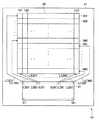
図1に示すように、このLCDモジュール18は、ドライバIC1と、LCDパネル20と、ガラス基板19とを含んでいる。即ち、ガラス基板19上にドライバIC1とLCDパネル20とが実装され、LCDモジュール18を構成している。
【0022】
LCDパネル20は、セグメント方向において複数の領域101、102、・・・を有し、コモン方向においても複数の領域301、302、・・・を有している。ここで、セグメント方向の1つの領域とコモン方向の1つの領域を特定することにより、1つの画素(ドット)が特定される。一例としては、LCDパネル20が、セグメント方向において160個の領域を有し、コモン方向においても160個の領域を有する。この場合には、LCDパネル20は、160×160の画素を有することになる。
【0023】
ドライバIC1は1つの方向に長い形状を有しており、その実装面の長手方向の一辺(図中上方の辺)の中央部に沿ってセグメント信号を出力するための金(Au)バンプのセグメント信号出力端子S1〜S160が形成されている。また、ドライバIC1の実装面の長手方向の一辺(図中上方の辺)の上記中央部の両側の部分に沿って、コモン信号を出力するための金(Au)バンプのコモン信号出力端子C1〜C80及びC81〜C160が形成されている。更に、ドライバIC1の実装面の長手方向の他辺(図中下方の辺)に沿って、金(Au)バンプの入出力端子P1〜Pnが形成されている。
【0024】
ガラス基板19上において、透明な配線LS1〜LS160及びLC1〜LC160が形成されている。LCDパネル20の領域101〜260には、配線LS1〜LS160によって、ドライバIC1のセグメント信号出力端子S1〜S160がそれぞれ接続されている。また、LCDパネル20の領域301〜380には、配線LC1〜LC80によって、ドライバIC1のコモン信号出力端子C1〜C80がそれぞれ接続され、LCDパネル20の領域381〜460には、配線LC160〜LC81によって、ドライバIC1のコモン信号出力端子C160〜C81がそれぞれ接続されている。
【0025】
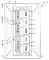
図2は、ドライバIC1の内部構成を示す図である。図2において、ドライバIC1は、パッケージ2と、パッケージ2に封入されたシリコン基板3とを含んでいる。
【0026】
シリコン基板3上の長手方向の一辺(図中上方の辺)の中央部に沿って、セグメント信号出力部4が形成されている。また、シリコン基板3上の長手方向の一辺(図中上方の辺)の上記中央部の両側に沿って、コモン信号出力部5〜6が形成されている。
【0027】
さらに、シリコン基板3上の長手方向の他辺(図中下方の辺)に沿って、コモン信号出力部5〜6に対向するように(図中コモン信号出力部5〜6の下部に)、電源部7〜8が分割して形成されている。また、シリコン基板3上の長手方向の他辺(図中下方の辺)に沿って、電源部7〜8の間に、RAM9〜10、及び、制御部11が形成されている。
【0028】
電源部7と電源部8とは、セグメント信号出力部4及びコモン信号出力部5〜6上を通過するように形成された電源配線12〜13によって接続されている。また、セグメント信号出力部4、コモン信号出力部5〜6、電源部7〜8、RAM9〜10、及び、制御部10は、配線(図示せず)によって相互に接続されている。
【0029】
セグメント信号出力部4は、セグメント信号出力端子S1〜S160に接続されており、これらのセグメント信号出力端子からセグメント信号を出力する。
コモン信号出力部5は、コモン信号出力端子C1〜C80に接続されており、これらのコモン信号出力端子からコモン信号を出力する。コモン信号出力部6は、コモン信号出力端子C81〜C160に接続されており、これらのコモン信号出力端子からコモン信号を出力する。
【0030】
電源部7〜8、RAM9〜10、及び、制御部10は、入力端子P1〜Pnに接続されており、これらの入力端子P1〜Pnから電源電位、制御信号、画像データ等の入力を行う。
電源部7〜8は、入力端子から電源電位を受けてレギュレーション等を行い、セグメント信号出力部4、コモン信号出力部5〜6、RAM9〜10、及び、制御部10に電源を供給する。また、電源部7〜8は、電源配線12〜13によって、レギュレーションにおける中間電位を互いに供給し合う。
RAM9〜10は、入力端子から画像データを受け取り、これを記憶する。
【0031】
制御部10は、ロジック回路であり、入力端子から制御信号等を受信し、セグメント信号出力部4、コモン信号出力部5〜6、電源部7〜8、及び、RAM9〜10の制御を行う。
【0032】
再び図1を参照すると、LCDドライバ1のセグメント出力端子S1〜S160からは、セグメント信号が順次出力される。一方、LCDドライバ1のコモン信号出力端子C1〜C80及びC160〜C81からは、上述したコモン信号出力部5〜6によってコモン信号が順次出力される。従って、LCDドライバ1によって、LCDパネル20を駆動することができる。
【0033】
本実施形態においては、LCDドライバ1内のコモン信号出力部5〜6が、シリコン基板3の短手方向ではなく長手方向の辺に沿って形成されている。そのため、シリコン基板3の短手方向の長さを短くすることができ、ドライバIC1の短手方向の長さを短くすることができる。従って、LCDモジュール18の額縁部を狭くしてスリム化することができる。また、電源配線12〜13がセグメント信号出力部4及びコモン信号出力部5〜6上を通過するように形成されており、これらの電源配線12〜13からセグメント信号出力部4、コモン信号出力部5〜6、RAM9〜10、及び、制御部10に中間電位が供給される。そのため、シリコン基板3上の電源を電源部7〜8の2つに分割して形成することにより必要となる配線等に起因して、シリコン基板3の面積が拡大することはない。
【0034】
【発明の効果】
以上述べた様に、本発明によれば、シリコン基板の長手方向の一辺の中央部に沿ってセグメント信号出力部を形成し、シリコン基板の長手方向の一辺の上記中央部の両側の部分に沿って第1及び第2のコモン信号出力部を形成し、シリコン基板の長手方向の他辺に沿って、第1及び第2のコモン信号出力部と対向するように第1及び第2の電源部を形成することにより、ドライバICの短手方向の長さを短くすることができる。これにより、LCDモジュールの額縁部を狭くしてスリム化を実現することが可能となる。
【図面の簡単な説明】
【図1】本発明の一実施形態に係る半導体装置を用いたLCDモジュールを示す図である。
【図2】本発明の一実施形態に係る半導体装置の構成を示す図である。
【図3】従来のドライバICを用いたLCDモジュールを示す図である。
【図4】従来のドライバICの構成を示す図である。
【符号の説明】
1、31 ドライバIC
2、32 パッケージ
3、33 シリコン基板
4、34 セグメント信号出力部
5〜6、35〜36 コモン信号出力部
7〜8、37 電源部
9〜10、39 RAM
11、38 制御部
12〜13 電源配線
C1〜C160、C201〜C360 コモン信号出力端子
S1〜S160、S201〜S360 セグメント信号出力端子
P1〜Pn、Q1〜Qn 入力端子
18、40 LCDモジュール
19、41 ガラス基板
20 LCDパネル
101、102、・・・ LCDパネルにおけるセグメント方向に分割された領域
301、302、・・・ LCDパネルにおけるコモン方向に分割された領域[0001]
BACKGROUND OF THE INVENTION
The present invention relates to a semiconductor device (driver IC) for driving a display device such as an LCD panel.
[0002]
[Prior art]
A conventional driver IC for driving an LCD panel will be described with reference to FIGS.
[0003]
FIG. 3 is a diagram showing an LCD module using a conventional semiconductor device. As shown in FIG. 3, the
[0004]
The
[0005]
The driver IC 31 has a long shape in one direction, and a segment of a gold (Au) bump for outputting a segment signal along the central portion of one side (the upper side in the figure) of the mounting surface in the longitudinal direction. Signal output terminals S201 to S360 are formed. Also, common signal output terminals C201 of gold (Au) bumps for outputting a common signal along the both sides of the central portion of one side (upper side in the drawing) of the mounting surface of the
[0006]
On the
[0007]
FIG. 4 is a diagram illustrating an internal configuration of the
[0008]
A segment
[0009]
The segment
The common
[0010]
The
The
[0011]
The
The
[0012]
Referring to FIG. 3 again, segment signals are sequentially output from the segment output terminals S201 to S360 of the
[0013]
[Problems to be solved by the invention]
In the above-described conventional driver IC 31, the common
[0014]
However, if the common
[0015]
Accordingly, in view of the above points, the present invention provides a semiconductor device that can shorten the length of the driver IC in the short direction and can achieve slimming by narrowing the frame portion of the LCD module. For the purpose.
[0016]
[Means for Solving the Problems]
In order to solve the above problems, a semiconductor device according to the present invention supplies a first group of drive signals to a first group of signal electrodes of an image display device that displays a two-dimensional image, A semiconductor device for supplying a second group of drive signals, which is formed in a first region along a semiconductor substrate and a first side in a longitudinal direction of the semiconductor substrate. A first output unit that outputs a predetermined number of drive signals and a second region that is adjacent to the first region along the first side and outputs a second group of drive signals. An output unit, a third output unit that is formed in a third region adjacent to the second region along the first side, and outputs a remaining drive signal of the first group of drive signals; and a semiconductor A first power source formed in the fourth region along the second side in the longitudinal direction of the substrate and supplying power to at least the first output unit When formed in a fifth region along a second side, and second power supply section for supplying power to at least a third output section.
[0017]
Here, it is formed in a sixth region between the fourth region and the fifth region along the second side, and sequentially input image data is stored in the first to third output units. A storage unit to be supplied may be further provided. In addition, it further includes wiring formed on the first to third output portions via an insulating film for exchanging potential between the first power supply portion and the second power supply portion. Also good. Further, the image display device is a liquid crystal display device, the first group of drive signals is a plurality of common signals supplied to a plurality of common electrodes of the liquid crystal display device, respectively, and the second group of drive signals is a plurality of liquid crystal display devices. It may be a plurality of segment signals respectively supplied to the segment electrodes.
[0018]
According to the present invention configured as described above, the length in the short direction of the semiconductor device for driving the image display device can be shortened, and the frame portion of the image display module is narrowed to achieve slimming. can do.
[0019]
DETAILED DESCRIPTION OF THE INVENTION
Hereinafter, embodiments of the present invention will be described with reference to the drawings. In addition, the same reference number is attached | subjected to the same component and description is abbreviate | omitted.
[0020]
FIG. 1 is a diagram showing an LCD module using a semiconductor device according to an embodiment of the present invention. In the present embodiment, the present invention is applied to an LCD driver IC.
[0021]
As shown in FIG. 1, the
[0022]
The
[0023]
The driver IC 1 has a long shape in one direction, and a segment of a gold (Au) bump for outputting a segment signal along the central portion of one side (the upper side in the figure) of the mounting surface in the longitudinal direction. Signal output terminals S1 to S160 are formed. Further, common signal output terminals C1 to C1 of gold (Au) bumps for outputting a common signal along one side of the central portion of one side (upper side in the drawing) of the mounting surface of the driver IC1. C80 and C81 to C160 are formed. Furthermore, input / output terminals P1 to Pn of gold (Au) bumps are formed along the other side in the longitudinal direction (the lower side in the drawing) of the mounting surface of the driver IC1.
[0024]
On the
[0025]
FIG. 2 is a diagram illustrating an internal configuration of the driver IC 1. In FIG. 2, the driver IC 1 includes a
[0026]
A segment
[0027]
Further, along the other side in the longitudinal direction on the silicon substrate 3 (lower side in the figure) so as to face the common
[0028]
The
[0029]
The segment
The common
[0030]
The
The
The
[0031]
The
[0032]
Referring again to FIG. 1, segment signals are sequentially output from the segment output terminals S1 to S160 of the LCD driver 1. On the other hand, common signals are sequentially output from the common signal output terminals C1 to C80 and C160 to C81 of the LCD driver 1 by the common
[0033]
In the present embodiment, the common
[0034]
【The invention's effect】
As described above, according to the present invention, the segment signal output portion is formed along the central portion of one side in the longitudinal direction of the silicon substrate, and along the portions on both sides of the central portion on one side in the longitudinal direction of the silicon substrate. Forming first and second common signal output sections, and first and second power supply sections facing the first and second common signal output sections along the other side in the longitudinal direction of the silicon substrate. As a result, the length of the driver IC in the short direction can be shortened. As a result, the frame portion of the LCD module can be narrowed to achieve slimming.
[Brief description of the drawings]
FIG. 1 is a diagram showing an LCD module using a semiconductor device according to an embodiment of the present invention.
FIG. 2 is a diagram showing a configuration of a semiconductor device according to an embodiment of the present invention.
FIG. 3 is a diagram showing an LCD module using a conventional driver IC.
FIG. 4 is a diagram showing a configuration of a conventional driver IC.
[Explanation of symbols]
1, 31 Driver IC
2, 32
11, 38 Control part 12-13 Power supply wiring C1-C160, C201-C360 Common signal output terminal S1-S160, S201-S360 Segment signal output terminal P1-Pn, Q1-
Claims (4)
Translated fromJapanese半導体基板と、
前記半導体基板の長手方向の第1の辺の一端側に沿って第1の領域に形成され、第1群の駆動信号の内の所定数の駆動信号を出力する第1の出力部と、
前記第1の辺の中央部に沿って前記第1の領域に隣接する第2の領域に形成され、第2群の駆動信号を出力する第2の出力部と、
前記第1の辺の他端側に沿って前記第2の領域に隣接する第3の領域に形成され、第1群の駆動信号の内の残りの駆動信号を出力する第3の出力部と、
前記半導体基板の長手方向の第2の辺に沿って前記第1の出力部と対向する第4の領域に形成され、少なくとも前記第1の出力部に供給する所定の電源電圧を発生する第1の電源部と、
前記第2の辺に沿って前記第3の出力部と対向する第5の領域に形成され、少なくとも前記第3の出力部に供給する所定の電源電圧を発生する第2の電源部と、
を具備する半導体装置。A semiconductor device for supplying a first group of drive signals to a first group of signal electrodes of an image display device for displaying a two-dimensional image and supplying a second group of drive signals to a second group of signal electrodes. ,
A semiconductor substrate;
A first output unit that is formed in a first region along one end side of the first side in the longitudinal direction of the semiconductor substrate and outputs a predetermined number of drive signals of the first group of drive signals;
A second output unit that is formed in a second region adjacent to the first region along a central portion of the first side and outputs a second group of drive signals;
A third output section that is formed in a third region adjacent to the second region along the other end side of the first side and outputs the remaining drive signals of the first group of drive signals; ,
A first region that is formed in a fourth region facing the first output unit along the second side in the longitudinal direction of the semiconductor substrate and generates at least a predetermined power supply voltage to be supplied to the first output unit. Power supply section of
A second power supply section that is formed in a fifth region facing the third output section along the second side and generates at least a predetermined power supply voltage to be supplied to the third output section;
A semiconductor device comprising:
Priority Applications (2)
| Application Number | Priority Date | Filing Date | Title |
|---|---|---|---|
| JP2000376296AJP4146613B2 (en) | 2000-12-11 | 2000-12-11 | Semiconductor device |
| US09/997,226US6771258B2 (en) | 2000-12-11 | 2001-11-29 | Semiconductor device |
Applications Claiming Priority (1)
| Application Number | Priority Date | Filing Date | Title |
|---|---|---|---|
| JP2000376296AJP4146613B2 (en) | 2000-12-11 | 2000-12-11 | Semiconductor device |
Publications (2)
| Publication Number | Publication Date |
|---|---|
| JP2002182232A JP2002182232A (en) | 2002-06-26 |
| JP4146613B2true JP4146613B2 (en) | 2008-09-10 |
Family
ID=18845171
Family Applications (1)
| Application Number | Title | Priority Date | Filing Date |
|---|---|---|---|
| JP2000376296AExpired - Fee RelatedJP4146613B2 (en) | 2000-12-11 | 2000-12-11 | Semiconductor device |
Country Status (2)
| Country | Link |
|---|---|
| US (1) | US6771258B2 (en) |
| JP (1) | JP4146613B2 (en) |
Families Citing this family (36)
| Publication number | Priority date | Publication date | Assignee | Title |
|---|---|---|---|---|
| JP2002270693A (en)* | 2001-03-06 | 2002-09-20 | Sanyo Electric Co Ltd | Semiconductor device and pattern layout method thereof |
| JP4165120B2 (en)* | 2002-05-17 | 2008-10-15 | 株式会社日立製作所 | Image display device |
| TW588322B (en)* | 2003-03-28 | 2004-05-21 | Au Optronics Corp | Liquid crystal display panel's integrated driver device frame |
| JP4186970B2 (en)* | 2005-06-30 | 2008-11-26 | セイコーエプソン株式会社 | Integrated circuit device and electronic apparatus |
| JP4010334B2 (en)* | 2005-06-30 | 2007-11-21 | セイコーエプソン株式会社 | Integrated circuit device and electronic apparatus |
| US20070001975A1 (en)* | 2005-06-30 | 2007-01-04 | Seiko Epson Corporation | Integrated circuit device and electronic instrument |
| US7755587B2 (en)* | 2005-06-30 | 2010-07-13 | Seiko Epson Corporation | Integrated circuit device and electronic instrument |
| JP4010336B2 (en)* | 2005-06-30 | 2007-11-21 | セイコーエプソン株式会社 | Integrated circuit device and electronic apparatus |
| JP2007043030A (en)* | 2005-06-30 | 2007-02-15 | Seiko Epson Corp | Integrated circuit device and electronic apparatus |
| JP4797802B2 (en)* | 2005-06-30 | 2011-10-19 | セイコーエプソン株式会社 | Integrated circuit device and electronic apparatus |
| JP4810935B2 (en)* | 2005-06-30 | 2011-11-09 | セイコーエプソン株式会社 | Integrated circuit device and electronic apparatus |
| JP4010332B2 (en)* | 2005-06-30 | 2007-11-21 | セイコーエプソン株式会社 | Integrated circuit device and electronic apparatus |
| JP4797804B2 (en)* | 2005-06-30 | 2011-10-19 | セイコーエプソン株式会社 | Integrated circuit device and electronic apparatus |
| JP4830371B2 (en)* | 2005-06-30 | 2011-12-07 | セイコーエプソン株式会社 | Integrated circuit device and electronic apparatus |
| US20070001984A1 (en)* | 2005-06-30 | 2007-01-04 | Seiko Epson Corporation | Integrated circuit device and electronic instrument |
| KR100828792B1 (en)* | 2005-06-30 | 2008-05-09 | 세이코 엡슨 가부시키가이샤 | Integrated circuit device and electronic instrument |
| JP4010335B2 (en)* | 2005-06-30 | 2007-11-21 | セイコーエプソン株式会社 | Integrated circuit device and electronic apparatus |
| JP4797801B2 (en)* | 2005-06-30 | 2011-10-19 | セイコーエプソン株式会社 | Integrated circuit device and electronic apparatus |
| US7764278B2 (en)* | 2005-06-30 | 2010-07-27 | Seiko Epson Corporation | Integrated circuit device and electronic instrument |
| JP4797803B2 (en)* | 2005-06-30 | 2011-10-19 | セイコーエプソン株式会社 | Integrated circuit device and electronic apparatus |
| JP4661400B2 (en) | 2005-06-30 | 2011-03-30 | セイコーエプソン株式会社 | Integrated circuit device and electronic apparatus |
| JP4797791B2 (en)* | 2005-06-30 | 2011-10-19 | セイコーエプソン株式会社 | Integrated circuit device and electronic apparatus |
| JP4951902B2 (en)* | 2005-06-30 | 2012-06-13 | セイコーエプソン株式会社 | Integrated circuit device and electronic apparatus |
| JP4151688B2 (en)* | 2005-06-30 | 2008-09-17 | セイコーエプソン株式会社 | Integrated circuit device and electronic apparatus |
| JP4010333B2 (en)* | 2005-06-30 | 2007-11-21 | セイコーエプソン株式会社 | Integrated circuit device and electronic apparatus |
| KR100850614B1 (en)* | 2005-06-30 | 2008-08-05 | 세이코 엡슨 가부시키가이샤 | Integrated circuit devices and electronic devices |
| JP4665677B2 (en) | 2005-09-09 | 2011-04-06 | セイコーエプソン株式会社 | Integrated circuit device and electronic apparatus |
| US7911498B2 (en)* | 2005-12-12 | 2011-03-22 | Novatek Microelectronics Corp. | Compensation device for non-uniform regions in flat panel display and method thereof |
| JP4650291B2 (en)* | 2006-02-10 | 2011-03-16 | セイコーエプソン株式会社 | Integrated circuit device and electronic apparatus |
| JP4586739B2 (en) | 2006-02-10 | 2010-11-24 | セイコーエプソン株式会社 | Semiconductor integrated circuit and electronic equipment |
| JP4889457B2 (en)* | 2006-11-30 | 2012-03-07 | 株式会社 日立ディスプレイズ | Liquid crystal display |
| JP4492694B2 (en)* | 2007-12-20 | 2010-06-30 | セイコーエプソン株式会社 | Integrated circuit device, electro-optical device and electronic apparatus |
| US20090160881A1 (en)* | 2007-12-20 | 2009-06-25 | Seiko Epson Corporation | Integrated circuit device, electro-optical device, and electronic instrument |
| JP4973482B2 (en)* | 2007-12-20 | 2012-07-11 | セイコーエプソン株式会社 | Integrated circuit device, electro-optical device and electronic apparatus |
| KR102050511B1 (en) | 2012-07-24 | 2019-12-02 | 삼성디스플레이 주식회사 | Display device |
| KR102276995B1 (en)* | 2015-02-12 | 2021-07-21 | 삼성디스플레이 주식회사 | Nonsquare display |
Family Cites Families (3)
| Publication number | Priority date | Publication date | Assignee | Title |
|---|---|---|---|---|
| US6525718B1 (en)* | 1997-02-05 | 2003-02-25 | Sharp Kabushiki Kaisha | Flexible circuit board and liquid crystal display device incorporating the same |
| JP2000039869A (en)* | 1998-07-22 | 2000-02-08 | Seiko Instruments Inc | Display controlling ic device and display device using the same |
| JP2002182614A (en)* | 2000-12-11 | 2002-06-26 | Seiko Epson Corp | Semiconductor device |
- 2000
- 2000-12-11JPJP2000376296Apatent/JP4146613B2/ennot_activeExpired - Fee Related
- 2001
- 2001-11-29USUS09/997,226patent/US6771258B2/ennot_activeExpired - Lifetime
Also Published As
| Publication number | Publication date |
|---|---|
| JP2002182232A (en) | 2002-06-26 |
| US20020080104A1 (en) | 2002-06-27 |
| US6771258B2 (en) | 2004-08-03 |
Similar Documents
| Publication | Publication Date | Title |
|---|---|---|
| JP4146613B2 (en) | Semiconductor device | |
| KR100497047B1 (en) | Display device | |
| JP3696512B2 (en) | Display element driving device and display device using the same | |
| KR101313918B1 (en) | Device board | |
| KR101113031B1 (en) | Pad layout structure of driver IC chip | |
| JPH0954333A (en) | Display device and IC chip used for the same | |
| EP1009028A2 (en) | Matrix type display apparatus, method of production thereof, and thermocompression bonding head | |
| US20090251387A1 (en) | Display device | |
| JP3638123B2 (en) | Display module | |
| JP2002040997A5 (en) | ||
| US20070109484A1 (en) | Drive element mount display | |
| US6707440B2 (en) | Semiconductor device | |
| JP2001188517A (en) | Display module | |
| KR101298156B1 (en) | Driver IC chip | |
| US7095406B2 (en) | Driving integrated circuit unit for a liquid crystal display device | |
| JPH08286202A (en) | Liquid crystal display | |
| JP4526415B2 (en) | Display device and glass substrate for display device | |
| JPH09258249A (en) | Semiconductor integrated circuit | |
| JP3884111B2 (en) | Video control device and flat display device provided with the video control device | |
| KR20100112861A (en) | Image display apparatus | |
| JPH08313925A (en) | Semiconductor integrated circuit | |
| JP2005136017A (en) | Display device | |
| JP4343328B2 (en) | Display device | |
| JP2004252178A (en) | Electro-optical panel, method of manufacturing electro-optical panel, electro-optical device, and electronic apparatus | |
| CN114660860A (en) | Display panel and display device |
Legal Events
| Date | Code | Title | Description |
|---|---|---|---|
| A621 | Written request for application examination | Free format text:JAPANESE INTERMEDIATE CODE: A621 Effective date:20040113 | |
| A977 | Report on retrieval | Free format text:JAPANESE INTERMEDIATE CODE: A971007 Effective date:20051129 | |
| A131 | Notification of reasons for refusal | Free format text:JAPANESE INTERMEDIATE CODE: A131 Effective date:20060718 | |
| A02 | Decision of refusal | Free format text:JAPANESE INTERMEDIATE CODE: A02 Effective date:20061212 | |
| A521 | Written amendment | Free format text:JAPANESE INTERMEDIATE CODE: A523 Effective date:20070209 | |
| A911 | Transfer of reconsideration by examiner before appeal (zenchi) | Free format text:JAPANESE INTERMEDIATE CODE: A911 Effective date:20070215 | |
| A912 | Removal of reconsideration by examiner before appeal (zenchi) | Free format text:JAPANESE INTERMEDIATE CODE: A912 Effective date:20070323 | |
| RD04 | Notification of resignation of power of attorney | Free format text:JAPANESE INTERMEDIATE CODE: A7424 Effective date:20070410 | |
| A01 | Written decision to grant a patent or to grant a registration (utility model) | Free format text:JAPANESE INTERMEDIATE CODE: A01 | |
| A61 | First payment of annual fees (during grant procedure) | Free format text:JAPANESE INTERMEDIATE CODE: A61 Effective date:20080620 | |
| R150 | Certificate of patent or registration of utility model | Ref document number:4146613 Country of ref document:JP Free format text:JAPANESE INTERMEDIATE CODE: R150 Free format text:JAPANESE INTERMEDIATE CODE: R150 | |
| FPAY | Renewal fee payment (event date is renewal date of database) | Free format text:PAYMENT UNTIL: 20110627 Year of fee payment:3 | |
| FPAY | Renewal fee payment (event date is renewal date of database) | Free format text:PAYMENT UNTIL: 20110627 Year of fee payment:3 | |
| FPAY | Renewal fee payment (event date is renewal date of database) | Free format text:PAYMENT UNTIL: 20120627 Year of fee payment:4 | |
| FPAY | Renewal fee payment (event date is renewal date of database) | Free format text:PAYMENT UNTIL: 20130627 Year of fee payment:5 | |
| FPAY | Renewal fee payment (event date is renewal date of database) | Free format text:PAYMENT UNTIL: 20130627 Year of fee payment:5 | |
| S531 | Written request for registration of change of domicile | Free format text:JAPANESE INTERMEDIATE CODE: R313531 | |
| R350 | Written notification of registration of transfer | Free format text:JAPANESE INTERMEDIATE CODE: R350 | |
| R250 | Receipt of annual fees | Free format text:JAPANESE INTERMEDIATE CODE: R250 | |
| LAPS | Cancellation because of no payment of annual fees |