JP4144640B2 - Method for manufacturing vibration sensor - Google Patents
Method for manufacturing vibration sensorDownload PDFInfo
- Publication number
- JP4144640B2 JP4144640B2JP2006280648AJP2006280648AJP4144640B2JP 4144640 B2JP4144640 B2JP 4144640B2JP 2006280648 AJP2006280648 AJP 2006280648AJP 2006280648 AJP2006280648 AJP 2006280648AJP 4144640 B2JP4144640 B2JP 4144640B2
- Authority
- JP
- Japan
- Prior art keywords
- semiconductor substrate
- thin film
- etching
- sacrificial layer
- etchant
- Prior art date
- Legal status (The legal status is an assumption and is not a legal conclusion. Google has not performed a legal analysis and makes no representation as to the accuracy of the status listed.)
- Active
Links
Images


Classifications
- H—ELECTRICITY
- H10—SEMICONDUCTOR DEVICES; ELECTRIC SOLID-STATE DEVICES NOT OTHERWISE PROVIDED FOR
- H10D—INORGANIC ELECTRIC SEMICONDUCTOR DEVICES
- H10D48/00—Individual devices not covered by groups H10D1/00 - H10D44/00
- H10D48/50—Devices controlled by mechanical forces, e.g. pressure
- B—PERFORMING OPERATIONS; TRANSPORTING
- B81—MICROSTRUCTURAL TECHNOLOGY
- B81C—PROCESSES OR APPARATUS SPECIALLY ADAPTED FOR THE MANUFACTURE OR TREATMENT OF MICROSTRUCTURAL DEVICES OR SYSTEMS
- B81C1/00—Manufacture or treatment of devices or systems in or on a substrate
- B81C1/00015—Manufacture or treatment of devices or systems in or on a substrate for manufacturing microsystems
- B81C1/00134—Manufacture or treatment of devices or systems in or on a substrate for manufacturing microsystems comprising flexible or deformable structures
- B81C1/00182—Arrangements of deformable or non-deformable structures, e.g. membrane and cavity for use in a transducer
- H—ELECTRICITY
- H01—ELECTRIC ELEMENTS
- H01L—SEMICONDUCTOR DEVICES NOT COVERED BY CLASS H10
- H01L21/00—Processes or apparatus adapted for the manufacture or treatment of semiconductor or solid state devices or of parts thereof
- H01L21/02—Manufacture or treatment of semiconductor devices or of parts thereof
- H01L21/04—Manufacture or treatment of semiconductor devices or of parts thereof the devices having potential barriers, e.g. a PN junction, depletion layer or carrier concentration layer
- H01L21/18—Manufacture or treatment of semiconductor devices or of parts thereof the devices having potential barriers, e.g. a PN junction, depletion layer or carrier concentration layer the devices having semiconductor bodies comprising elements of Group IV of the Periodic Table or AIIIBV compounds with or without impurities, e.g. doping materials
- H01L21/30—Treatment of semiconductor bodies using processes or apparatus not provided for in groups H01L21/20 - H01L21/26
- H01L21/302—Treatment of semiconductor bodies using processes or apparatus not provided for in groups H01L21/20 - H01L21/26 to change their surface-physical characteristics or shape, e.g. etching, polishing, cutting
- H01L21/306—Chemical or electrical treatment, e.g. electrolytic etching
- H—ELECTRICITY
- H04—ELECTRIC COMMUNICATION TECHNIQUE
- H04R—LOUDSPEAKERS, MICROPHONES, GRAMOPHONE PICK-UPS OR LIKE ACOUSTIC ELECTROMECHANICAL TRANSDUCERS; DEAF-AID SETS; PUBLIC ADDRESS SYSTEMS
- H04R19/00—Electrostatic transducers
- H04R19/005—Electrostatic transducers using semiconductor materials
- H—ELECTRICITY
- H04—ELECTRIC COMMUNICATION TECHNIQUE
- H04R—LOUDSPEAKERS, MICROPHONES, GRAMOPHONE PICK-UPS OR LIKE ACOUSTIC ELECTROMECHANICAL TRANSDUCERS; DEAF-AID SETS; PUBLIC ADDRESS SYSTEMS
- H04R19/00—Electrostatic transducers
- H04R19/04—Microphones
- B—PERFORMING OPERATIONS; TRANSPORTING
- B81—MICROSTRUCTURAL TECHNOLOGY
- B81B—MICROSTRUCTURAL DEVICES OR SYSTEMS, e.g. MICROMECHANICAL DEVICES
- B81B2201/00—Specific applications of microelectromechanical systems
- B81B2201/02—Sensors
- B81B2201/0257—Microphones or microspeakers
- B—PERFORMING OPERATIONS; TRANSPORTING
- B81—MICROSTRUCTURAL TECHNOLOGY
- B81B—MICROSTRUCTURAL DEVICES OR SYSTEMS, e.g. MICROMECHANICAL DEVICES
- B81B2201/00—Specific applications of microelectromechanical systems
- B81B2201/02—Sensors
- B81B2201/0285—Vibration sensors
- B—PERFORMING OPERATIONS; TRANSPORTING
- B81—MICROSTRUCTURAL TECHNOLOGY
- B81B—MICROSTRUCTURAL DEVICES OR SYSTEMS, e.g. MICROMECHANICAL DEVICES
- B81B2203/00—Basic microelectromechanical structures
- B81B2203/01—Suspended structures, i.e. structures allowing a movement
- B81B2203/0127—Diaphragms, i.e. structures separating two media that can control the passage from one medium to another; Membranes, i.e. diaphragms with filtering function
- B—PERFORMING OPERATIONS; TRANSPORTING
- B81—MICROSTRUCTURAL TECHNOLOGY
- B81B—MICROSTRUCTURAL DEVICES OR SYSTEMS, e.g. MICROMECHANICAL DEVICES
- B81B2203/00—Basic microelectromechanical structures
- B81B2203/03—Static structures
- B81B2203/0353—Holes
Landscapes
- Engineering & Computer Science (AREA)
- Physics & Mathematics (AREA)
- Acoustics & Sound (AREA)
- Signal Processing (AREA)
- Manufacturing & Machinery (AREA)
- Microelectronics & Electronic Packaging (AREA)
- Condensed Matter Physics & Semiconductors (AREA)
- General Physics & Mathematics (AREA)
- Computer Hardware Design (AREA)
- Power Engineering (AREA)
- Pressure Sensors (AREA)
- Electrostatic, Electromagnetic, Magneto- Strictive, And Variable-Resistance Transducers (AREA)
- Weting (AREA)
Description
Translated fromJapanese本発明は、振動センサの製造方法に関し、特にダイアフラムのような素子薄膜を備えた振動センサの製造方法に関する。The present invention relates toa methodof manufacturinga vibrationsensor, a method of manufacturinga vibrationsensor which in particular comprises a device thin film such as a diaphragm.
半導体集積回路製造技術を応用して、シリコン基板上に単結晶シリコンや多結晶シリコンを積層させて薄膜を形成し、この薄膜をダイアフラムとして用いる振動センサが開発されてきている。シリコンから成るダイアフラムはアルミニウムやチタンなどの金属に比べて内部応力が少なく、また密度が低いために、高感度の振動センサが得られるとともに、半導体集積回路製造工程との整合性も良い。このようなダイアフラムを有する振動センサとしては、例えば特許文献1に開示されたコンデンサマイクロフォンがある。このコンデンサマイクロフォンにあっては、単結晶シリコン(100)面からなる半導体基板の表面にダイアフラム(可動電極)と固定電極を形成した後、当該半導体基板の裏面外周部にエッチング用マスクを形成し、裏面側から表面に達するまで半導体基板をエッチングし、半導体基板の中央部に貫通孔をあけている。その結果、ダイアフラムは、その周囲を半導体基板の表面に固定され、中央部が貫通孔の上で中空支持され、音声振動などによって振動可能となる。 By applying semiconductor integrated circuit manufacturing technology, a vibration sensor has been developed in which a single crystal silicon or polycrystalline silicon is laminated on a silicon substrate to form a thin film, and this thin film is used as a diaphragm. A diaphragm made of silicon has less internal stress and a lower density than metals such as aluminum and titanium, so that a highly sensitive vibration sensor can be obtained and compatibility with a semiconductor integrated circuit manufacturing process is good. As a vibration sensor having such a diaphragm, there is a condenser microphone disclosed in Patent Document 1, for example. In this capacitor microphone, after forming a diaphragm (movable electrode) and a fixed electrode on the surface of a semiconductor substrate made of a single crystal silicon (100) surface, an etching mask is formed on the outer periphery of the back surface of the semiconductor substrate, The semiconductor substrate is etched from the back side to the surface, and a through hole is formed in the center of the semiconductor substrate. As a result, the periphery of the diaphragm is fixed to the surface of the semiconductor substrate, and the central portion is hollowly supported on the through hole, and can be vibrated by sound vibration or the like.
しかしながら、このような構造のコンデンサマイクロフォンでは、(100)面半導体基板を裏面側から結晶異方性エッチングするため、貫通孔の内周面には(111)面による傾斜面が出現し、貫通孔は裏面側で大きく開口した角錐台状の空間となる。そのためダイアフラムの面積に比べて貫通孔の裏面側における開口面積が大きくなり、コンデンサマイクロフォンの小型化が困難であった。なお、半導体基板の厚みを薄くすれば、貫通孔の表面の開口面積に対する裏面の開口面積の比率を小さくすることができるが、半導体基板の強度が低下するために製造時の取り扱いが難しくなり、半導体基板の厚みを薄くするにも限度がある。 However, in the capacitor microphone having such a structure, since the (100) plane semiconductor substrate is crystal-anisotropically etched from the back side, an inclined surface due to the (111) plane appears on the inner peripheral surface of the through hole. Is a truncated pyramid-shaped space that is greatly open on the back side. Therefore, the opening area on the back surface side of the through hole is larger than the area of the diaphragm, and it is difficult to reduce the size of the condenser microphone. If the thickness of the semiconductor substrate is reduced, the ratio of the opening area of the back surface to the opening area of the surface of the through hole can be reduced, but the handling of the semiconductor substrate becomes difficult because the strength of the semiconductor substrate is reduced, There is a limit to reducing the thickness of the semiconductor substrate.
また、特許文献2に記載された膜型センサでは、いわゆるDRIE(Deep Reactive Ion Etching)やICP(誘導結合プラズマ)などの垂直エッチングによって、半導体基板に裏面側から貫通孔を開口している。従って、貫通孔が角錐台状に広がらない分だけ膜型センサの小型化を図ることができる。しかしながら、DRIEやICPなどの装置では、装置価格が高価であると共にウエハの加工が枚様式であり、生産性が悪かった。 In the film type sensor described in Patent Document 2, a through hole is opened from the back surface side of the semiconductor substrate by vertical etching such as so-called DRIE (Deep Reactive Ion Etching) or ICP (Inductively Coupled Plasma). Therefore, it is possible to reduce the size of the membrane sensor by the amount that the through hole does not spread in a truncated pyramid shape. However, in apparatuses such as DRIE and ICP, the price of the apparatus is expensive and the wafer processing is in a single sheet form, so that productivity is poor.
また、表面側(ダイアフラム側)から半導体基板を結晶異方性エッチングする方法もあるが、このような方法ではダイアフラムにエッチングホールを開口しなければならず、時としてエッチングホールがダイアフラムの振動特性や強度等に悪影響を及ぼす恐れがあった。 In addition, there is a method of crystal anisotropic etching of a semiconductor substrate from the surface side (diaphragm side), but in such a method, an etching hole has to be opened in the diaphragm, and sometimes the etching hole has a vibration characteristic of the diaphragm or There was a risk of adverse effects on strength, etc.
なお(100)面半導体基板を裏面側から結晶異方性エッチングして基板に貫通孔を形成し、かつ表面の開口面積に対する裏面の開口面積の比率を小さくすることができるエッチング方法としては、特許文献3に記載された方法がある。この方法にあっては、半導体基板であるシリコンウエハ表面上の開口させたい矩形領域にまず犠牲層を形成し、その上に窒化シリコンから成る薄膜を蒸着させているので、シリコンウエハ裏面の開口面積は、異方性エッチングによって貫通孔がこの犠牲層に到達することができるだけの大きさがあればよい。 As an etching method capable of forming a through hole in the substrate by crystal anisotropic etching of the (100) plane semiconductor substrate from the back side, and reducing the ratio of the opening area of the back surface to the opening area of the front surface, a patent is disclosed. There is a method described in Document 3. In this method, a sacrificial layer is first formed in a rectangular region to be opened on the surface of a silicon wafer, which is a semiconductor substrate, and a thin film made of silicon nitride is deposited on the sacrificial layer. It is sufficient that the through hole has a size that can reach the sacrificial layer by anisotropic etching.
しかしながら、このエッチング方法では、表面の犠牲層をエッチングした後の基板をエッチングする際に、薄膜が基板のエッチャントにさらされるため、薄膜の材料として単結晶シリコンや多結晶シリコンを使用することができない。また、薄膜が基板上に直接形成されるため、薄膜の応力制御やベントホール等、振動センサの特性を向上させるための工程や構造を組み込むことが困難である。よって特許文献3に開示されたエッチング方法は、マイクロフォン等の高い感度を必要とする振動センサの製造方法としては適していなかった。 However, in this etching method, since the thin film is exposed to the etchant of the substrate when the substrate after etching the sacrificial layer on the surface is etched, it is not possible to use single crystal silicon or polycrystalline silicon as the material of the thin film. . In addition, since the thin film is formed directly on the substrate, it is difficult to incorporate a process or structure for improving the characteristics of the vibration sensor, such as stress control of the thin film and vent holes. Therefore, the etching method disclosed in Patent Document 3 is not suitable as a method for manufacturing a vibration sensor that requires high sensitivity such as a microphone.
本発明は上記のような技術的課題に鑑みてなされたものであり、その目的とするところは、小型でかつ生産性が高く、しかも振動特性に優れた振動センサの製造方法を提供することにある。The present invention has been made in view of the technical problems described above, it is an object of small size and high productivity, yet to provide a methodfor manufacturinga vibrationsensor having excellent vibration characteristics It is in.
本発明にかかる第1の振動センサの製造方法は、単結晶シリコンからなる半導体基板の表面の一部に、前記半導体基板をエッチングするためのエッチャントによって等方的にエッチングされる材料で犠牲層を形成する工程と、前記犠牲層および前記犠牲層の周囲の前記半導体基板の表面の上に、前記エッチャントに対して耐性を有する材料で素子薄膜保護膜を形成する工程と、前記犠牲層の上方に、単結晶シリコン、多結晶シリコンもしくはアモルファスシリコンからなる素子薄膜を形成する工程と、前記半導体基板の裏面に形成された、前記半導体基板をエッチングするためのエッチャントに対して耐性を有する裏面保護膜に裏面エッチング窓を開口する工程と、前記裏面エッチング窓からエッチャントを適用して前記半導体基板を裏面側から結晶異方性エッチングすることにより、当該エッチングが前記半導体基板の表面に達したときに前記エッチャントによって前記犠牲層を等方性エッチングさせ、前記犠牲層がエッチング除去された跡の空間に広がった前記エッチャントによって前記半導体基板を表面側から結晶異方性エッチングさせ、前記半導体基板に貫通孔を形成する工程と、前記素子薄膜保護膜を一部を残して除去し、残された前記素子薄膜保護膜によって前記半導体基板の上面で前記素子薄膜を支持するための保持部を設ける工程とを有することを特徴としている。 According to the first vibration sensor manufacturing method of the present invention, a sacrificial layer is formed on a part of a surface of a semiconductor substrate made of single crystal silicon with a material that is isotropically etched by an etchant for etching the semiconductor substrate. Forming a device thin film protective film with a material having resistance to the etchant on the sacrificial layer and the surface of the semiconductor substrate around the sacrificial layer; and above the sacrificial layer Forming a device thin film made of single crystal silicon, polycrystalline silicon, or amorphous silicon, and a back surface protective film formed on the back surface of the semiconductor substrate and resistant to an etchant for etching the semiconductor substrate. A step of opening a back surface etching window; and applying an etchant from the back surface etching window to remove the semiconductor substrate from the back surface side The crystal anisotropic etching causes the sacrificial layer to be isotropically etched by the etchant when the etching reaches the surface of the semiconductor substrate, and the sacrificial layer is spread in the space where the sacrificial layer has been etched away. A step of crystal anisotropic etching of the semiconductor substrate from the surface side by the etchant to form a through-hole in the semiconductor substrate, the element thin film protective film is removed leaving a part, and the remaining element thin film protection And a step of providing a holding portion for supporting the element thin film on the upper surface of the semiconductor substrate by a film.
本発明の第1の振動センサの製造方法によれば、単結晶シリコンからなる半導体基板を表裏両面から結晶異方性エッチングして貫通孔を形成しているので、貫通孔の開口面積が素子薄膜の面積に比べて大きくなり過ぎることが無く、振動センサの小型化を図ることができる。よって、1枚のウエハから作製できる素子数が増加し、振動センサを低コスト化することができる。また、第1の振動センサの製造方法によれば、1回のエッチング工程によって両面から貫通孔を形成できるので、製造工程が簡略化される。また、犠牲層と素子薄膜の間に保護層を形成しているため、前記素子薄膜が半導体基板のエッチャントに対して耐性を有さない材料で形成されている場合であっても、貫通孔を形成する際に素子薄膜がエッチャントで侵されるのを防止することができる。さらに前記素子薄膜は、単結晶シリコン、多結晶シリコンもしくはアモルファスシリコンで形成されているため、生産性が高く、しかも高感度の振動センサが得られる。 According to the first method for manufacturing a vibration sensor of the present invention, the through hole is formed by crystal anisotropic etching of the semiconductor substrate made of single crystal silicon from both the front and back surfaces. Therefore, the vibration sensor can be reduced in size. Therefore, the number of elements that can be manufactured from one wafer is increased, and the cost of the vibration sensor can be reduced. In addition, according to the first method for manufacturing a vibration sensor, the through hole can be formed from both sides by a single etching process, so that the manufacturing process is simplified. In addition, since a protective layer is formed between the sacrificial layer and the element thin film, even if the element thin film is formed of a material that does not have resistance to the etchant of the semiconductor substrate, the through hole is formed. It is possible to prevent the element thin film from being attacked by the etchant during the formation. Further, since the element thin film is formed of single crystal silicon, polycrystalline silicon or amorphous silicon, a highly sensitive vibration sensor with high productivity can be obtained.
本発明にかかる第2の振動センサの製造方法は、単結晶シリコンからなる半導体基板の表面の一部に、前記半導体基板をエッチングするための第1のエッチャントに対して耐性を有する材料で犠牲層を形成する工程と、前記犠牲層および前記犠牲層の周囲の前記半導体基板の表面の上に、前記第1のエッチャントに対して耐性を有する材料で素子薄膜保護膜を形成する工程と、前記犠牲層の上方に、単結晶シリコン、多結晶シリコンもしくはアモルファスシリコンからなる素子薄膜を形成する工程と、前記半導体基板の裏面に形成された、前記半導体基板をエッチングするためのエッチャントに対して耐性を有する裏面保護膜に裏面エッチング窓を開口する工程と、前記裏面エッチング窓から第1のエッチャントを適用して前記半導体基板を裏面側から結晶異方性エッチングする工程と、前記第1のエッチャントによるエッチングが前記半導体基板の表面に達した後、前記半導体基板の裏面側から第2のエッチャントを適用することによって前記犠牲層を等方性エッチングする工程と、前記犠牲層がエッチング除去された後、前記犠牲層がエッチング除去された跡の空間に前記半導体基板の裏面側から再び前記第1のエッチャントを適用することによって前記半導体基板を表面側から結晶異方性エッチングし、前記半導体基板に貫通孔を形成する工程と、前記素子薄膜保護膜を一部を残して除去し、残された前記素子薄膜保護膜によって前記半導体基板の上面で前記素子薄膜を支持するための保持部を設ける工程とを有することを特徴としている。 According to the second vibration sensor manufacturing method of the present invention, a sacrificial layer is formed on a part of a surface of a semiconductor substrate made of single crystal silicon with a material resistant to the first etchant for etching the semiconductor substrate. Forming an element thin film protective film with a material resistant to the first etchant on the sacrificial layer and the surface of the semiconductor substrate around the sacrificial layer, and the sacrificial layer A step of forming a device thin film made of single crystal silicon, polycrystalline silicon, or amorphous silicon above the layer; and an etchant formed on the back surface of the semiconductor substrate for etching the semiconductor substrate. A step of opening a back surface etching window in the back surface protective film; and applying the first etchant from the back surface etching window to form the semiconductor substrate. The step of crystal anisotropic etching from the surface side and the etching by the first etchant reaches the surface of the semiconductor substrate, and then the second etchant is applied from the back side of the semiconductor substrate to form the sacrificial layer. An isotropic etching step, and after the sacrificial layer is removed by etching, the first etchant is applied again from the back side of the semiconductor substrate to the space where the sacrificial layer has been removed by etching. A step of crystal anisotropic etching from the surface side to form a through-hole in the semiconductor substrate, the element thin film protective film is removed leaving a part, and the semiconductor thin film protective film by the remaining element thin film protective film And a step of providing a holding portion for supporting the element thin film on the upper surface.
本発明の第2の振動センサの製造方法によれば、半導体基板を表裏両面から結晶異方性エッチングして貫通孔を形成しているので、貫通孔の開口面積が素子薄膜の面積に比べて大きくなり過ぎることが無く、振動センサの小型化を図ることができる。よって、1枚のウエハから作製できる素子数が増加し、振動センサを低コスト化することができる。しかも、第2の振動センサの製造方法によれば、貫通孔の結晶異方性エッチングの工程と犠牲層をエッチングする工程とでエッチャントを切り替えているので、第1のエッチャントと第2のエッチャントを選択する際の制約が少なくなる。さらに前記素子薄膜は、単結晶シリコン、多結晶シリコンもしくはアモルファスシリコンで形成されているため、生産性が高く、しかも高感度の振動センサが得られる。 According to the second method for manufacturing a vibration sensor of the present invention, since the through hole is formed by crystal anisotropic etching of the semiconductor substrate from both the front and back surfaces, the opening area of the through hole is smaller than the area of the element thin film. The vibration sensor can be reduced in size without becoming too large. Therefore, the number of elements that can be manufactured from one wafer is increased, and the cost of the vibration sensor can be reduced. Moreover, according to the second method for manufacturing a vibration sensor, the etchant is switched between the crystal anisotropic etching step of the through hole and the step of etching the sacrificial layer, so that the first etchant and the second etchant are replaced with each other. There are fewer restrictions on selection. Further, since the element thin film is formed of single crystal silicon, polycrystalline silicon or amorphous silicon, a highly sensitive vibration sensor with high productivity can be obtained.
本発明の第1又は第2の振動センサの製造方法のある実施態様は、前記素子薄膜の表面側と裏面側とを連通させるためのベントホールを前記保持部間に形成することを特徴としている。かかる実施態様によれば、長さの長いベントホールを形成することができるので、マイクロフォンなどに用いた場合には、その音響抵抗を大きくでき、良好な音響特性を得ることができる。また、ベントホールで素子薄膜の表面側と裏面側を連通させることができるので、素子薄膜の表裏における静的圧力を均衡させることができる。 An embodiment of the first or second method for manufacturing a vibration sensor according to the present invention is characterized in that a vent hole for communicating the surface side and the back side of the element thin film is formed between the holding portions. . According to this embodiment, since a long vent hole can be formed, when used in a microphone or the like, the acoustic resistance can be increased and good acoustic characteristics can be obtained. Further, since the front surface side and the back surface side of the element thin film can be communicated with each other through the vent hole, the static pressure on the front and back surfaces of the element thin film can be balanced.
本発明の第1又は第2の振動センサの製造方法の別な実施態様は、前記素子薄膜が矩形であることを特徴としている。かかる実施態様によれば、単結晶シリコン基板の結晶異方性エッチングにより形成される開口部を有効に利用することができる。 Another embodiment of the method for manufacturing the first or second vibration sensor of the present invention is characterized in that the element thin film is rectangular. According to this embodiment, it is possible to effectively use the opening formed by crystal anisotropic etching of the single crystal silicon substrate.
本発明の第1又は第2の振動センサの製造方法のさらに別な実施態様は、前記保持部を前記素子薄膜の四隅に設けている。かかる実施態様によれば、素子薄膜が柔軟に変形できるようになるので、振動センサの感度が向上する。 In still another embodiment of the first or second vibration sensor manufacturing method of the present invention, the holding portions are provided at the four corners of the element thin film. According to such an embodiment, the element thin film can be flexibly deformed, so that the sensitivity of the vibration sensor is improved.
本発明の第1又は第2の振動センサの製造方法のさらに別な実施態様は、前記犠牲層を前記素子薄膜の形成領域の一部に設けておくことにより、前記素子薄膜を屈曲させている。かかる実施態様によれば、素子薄膜の変位を大きくしたり、応力による撓みを少なくできる。 In still another embodiment of the first or second vibration sensor manufacturing method of the present invention, the element thin film is bent by providing the sacrificial layer in a part of the element thin film formation region. . According to this embodiment, the displacement of the element thin film can be increased, and the bending due to stress can be reduced.
本発明の第1又は第2の振動センサの製造方法のさらに別な実施態様は、前記犠牲層を前記素子薄膜の形成領域の一部に設けておくことにより、前記素子薄膜の表面に突起を形成している。かかる実施態様によれば、素子薄膜の上方に電極などが配置されている場合に、変形した素子薄膜が電極などに面接触して貼り付いてしまうのを防止できる。 According to still another embodiment of the first or second method for manufacturing a vibration sensor of the present invention, a protrusion is formed on the surface of the element thin film by providing the sacrificial layer in a part of the element thin film formation region. Forming. According to this embodiment, when an electrode or the like is disposed above the element thin film, the deformed element thin film can be prevented from sticking to the electrode or the like in surface contact.
本発明の第1又は第2の振動センサの製造方法のさらに別な実施態様は、前記貫通孔の表面の開口面積よりも、前記貫通孔の内部の、前記開口と平行な断面の面積の方が大きいことを特徴としている。かかる実施態様によれば、貫通孔の体積を大きくすることができるので、振動センサを音響センサに用いたときに音響コンプライアンスを大きくできる。 Still another embodiment of the method for manufacturing the first or second vibration sensor of the present invention is that the area of the cross section parallel to the opening inside the through hole is larger than the opening area of the surface of the through hole. Is characterized by large. According to this embodiment, since the volume of the through hole can be increased, acoustic compliance can be increased when the vibration sensor is used as an acoustic sensor.
本発明の第1の振動センサの製造方法の別な実施態様は、前記犠牲層が多結晶シリコンもしくはアモルファスシリコンであることを特徴としている。かかる実施態様によれば、単結晶シリコンからなる半導体基板をエッチングすると同時に犠牲層をエッチングでき、工程が簡略化できる。また、多結晶シリコンやアモルファスシリコンは温度耐性が高いため、後工程に高温プロセスを用いることができるとともに、半導体集積回路製造工程との整合性も良い。 Another embodiment of the method for producing a first vibration sensor of the present invention is characterized in that the sacrificial layer is polycrystalline silicon or amorphous silicon. According to such an embodiment, the sacrificial layer can be etched simultaneously with the etching of the semiconductor substrate made of single crystal silicon, and the process can be simplified. In addition, since polycrystalline silicon and amorphous silicon have high temperature resistance, a high-temperature process can be used in a subsequent process, and compatibility with a semiconductor integrated circuit manufacturing process is good.
本発明の第1のマイクロフォンの製造方法は、単結晶シリコンからなる半導体基板の表面の一部に、前記半導体基板をエッチングするためのエッチャントによって等方的にエッチングされる材料で犠牲層を形成する工程と、前記犠牲層および前記犠牲層の周囲の前記半導体基板の表面の上に、前記エッチャントに対して耐性を有する材料で素子薄膜保護膜を形成する工程と、前記犠牲層の上方に、単結晶シリコン、多結晶シリコンもしくはアモルファスシリコンからなる素子薄膜を形成する工程と、前記素子薄膜の上方に固定電極を形成する工程と、前記半導体基板の裏面に形成された、前記半導体基板をエッチングするためのエッチャントに対して耐性を有する裏面保護膜に裏面エッチング窓を開口する工程と、前記裏面エッチング窓からエッチャントを適用して前記半導体基板を裏面側から結晶異方性エッチングすることにより、当該エッチングが前記半導体基板の表面に達したときに前記エッチャントによって前記犠牲層を等方性エッチングさせ、前記犠牲層がエッチング除去された跡の空間に広がった前記エッチャントによって前記半導体基板を表面側から結晶異方性エッチングさせ、前記半導体基板に貫通孔を形成する工程と、前記素子薄膜保護膜を一部を残して除去し、残された前記素子薄膜保護膜によって前記半導体基板の上面で前記素子薄膜を支持するための保持部を設ける工程とを有することを特徴としている。 In the first microphone manufacturing method of the present invention, a sacrificial layer is formed on a part of the surface of a semiconductor substrate made of single crystal silicon with a material that is isotropically etched by an etchant for etching the semiconductor substrate. A step of forming an element thin film protective film with a material resistant to the etchant on the sacrificial layer and the surface of the semiconductor substrate around the sacrificial layer, and above the sacrificial layer, A step of forming an element thin film made of crystalline silicon, polycrystalline silicon, or amorphous silicon; a step of forming a fixed electrode above the element thin film; and etching the semiconductor substrate formed on the back surface of the semiconductor substrate A step of opening a back surface etching window in the back surface protection film having resistance against the etchant of the back surface, and from the back surface etching window The sacrificial layer is isotropically etched by the etchant when the etching reaches the surface of the semiconductor substrate by applying anisotropic etching to the semiconductor substrate from the back surface side by applying an etchant. The semiconductor substrate is crystal-anisotropically etched from the surface side by the etchant that has spread in the space of the traces from which etching has been removed, and a through hole is formed in the semiconductor substrate, leaving a part of the device thin film protective film. And a step of providing a holding portion for supporting the element thin film on the upper surface of the semiconductor substrate by the remaining element thin film protective film.
本発明の第1のマイクロフォンの製造方法によれば、半導体基板を表裏両面から結晶異方性エッチングして貫通孔を形成しているので、貫通孔の開口面積が素子薄膜の面積に比べて大きくなり過ぎることが無く、振動センサの小型化を図ることができる。よって、1枚のウエハから作製できる素子数が増加し、振動センサを低コスト化することができる。また、第1の振動センサの製造方法によれば、半導体基板の裏面側から結晶異方性エッチングを開始して半導体基板を表裏両面から結晶異方性エッチングできるので、素子薄膜にエッチングホールを設ける必要が無く、素子薄膜の強度を低下させたり、素子薄膜の特性を変化させたりする恐れがない。しかも、第1の振動センサの製造方法によれば、1回のエッチング工程によって両面から貫通孔を形成できるので、製造工程が簡略化される。According to the first microphonemanufacturing method of the present invention, the through hole is formed by crystal anisotropic etching of the semiconductor substrate from both the front and back surfaces, so that the opening area of the through hole is larger than the area of the element thin film. The vibration sensor can be reduced in size without becoming too much. Therefore, the number of elements that can be manufactured from one wafer is increased, and the cost of the vibration sensor can be reduced. Further, according to the first vibration sensor manufacturing method, since crystal anisotropic etching can be started from the back surface side of the semiconductor substrate and the semiconductor substrate can be crystal anisotropic etched from both the front and back surfaces, an etching hole is provided in the element thin film. There is no need to reduce the strength of the element thin film or change the characteristics of the element thin film. Moreover, according to the first method for manufacturing a vibration sensor, the through-hole can be formed from both sides by a single etching process, so that the manufacturing process is simplified.
本発明の第2のマイクロフォンの製造方法は、単結晶シリコンからなる半導体基板の表面の一部に、前記半導体基板をエッチングするための第1のエッチャントに対して耐性を有する材料で犠牲層を形成する工程と、前記犠牲層および前記犠牲層の周囲の前記半導体基板の表面の上に、前記第1のエッチャントに対して耐性を有する材料で素子薄膜保護膜を形成する工程と、前記犠牲層の上方に、単結晶シリコン、多結晶シリコンもしくはアモルファスシリコンからなる素子薄膜を形成する工程と、前記素子薄膜の上方に固定電極を形成する工程と、前記半導体基板の裏面に形成された、前記半導体基板をエッチングするためのエッチャントに対して耐性を有する裏面保護膜に裏面エッチング窓を開口する工程と、前記裏面エッチング窓から第1のエッチャントを適用して前記半導体基板を裏面側から結晶異方性エッチングする工程と、前記第1のエッチャントによるエッチングが前記半導体基板の表面に達した後、前記半導体基板の裏面側から第2のエッチャントを適用することによって前記犠牲層を等方性エッチングする工程と、前記犠牲層がエッチング除去された後、前記犠牲層がエッチング除去された跡の空間に前記半導体基板の裏面側から再び前記第1のエッチャントを適用することによって前記半導体基板を表面側から結晶異方性エッチングし、前記半導体基板に貫通孔を形成する工程と、前記素子薄膜保護膜を一部を残して除去し、残された前記素子薄膜保護膜によって前記半導体基板の上面で前記素子薄膜を支持するための保持部を設ける工程とを有することを特徴としている。 According to the second microphone manufacturing method of the present invention, a sacrificial layer is formed on a part of the surface of a semiconductor substrate made of single crystal silicon with a material resistant to the first etchant for etching the semiconductor substrate. Forming an element thin film protective film on the sacrificial layer and a surface of the semiconductor substrate around the sacrificial layer with a material resistant to the first etchant; and A step of forming a device thin film made of single crystal silicon, polycrystalline silicon, or amorphous silicon, a step of forming a fixed electrode above the device thin film, and the semiconductor substrate formed on the back surface of the semiconductor substrate. A step of opening a back surface etching window in a back surface protective film having resistance to an etchant for etching, and from the back surface etching window A step of applying anisotropic etching to the semiconductor substrate from the back surface side and applying etching by the first etchant to the surface of the semiconductor substrate; Applying the etchant, and isotropically etching the sacrificial layer; and after the sacrificial layer is removed by etching, the sacrificial layer is removed from the back side of the semiconductor substrate in a space where the sacrificial layer is removed by etching. Applying a first etchant to crystal anisotropically etch the semiconductor substrate from the surface side, forming a through hole in the semiconductor substrate, removing the element thin film protective film leaving a part, Providing a holding part for supporting the element thin film on the upper surface of the semiconductor substrate by the element thin film protective film formed. It is set to.
本発明の第2のマイクロフォンの製造方法によれば、半導体基板を表裏両面から結晶異方性エッチングして貫通孔を形成しているので、貫通孔の開口面積が素子薄膜の面積に比べて大きくなり過ぎることが無く、振動センサの小型化を図ることができる。よって、1枚のウエハから作製できる素子数が増加し、振動センサを低コスト化することができる。また、第1の振動センサの製造方法によれば、半導体基板の裏面側から結晶異方性エッチングを開始して半導体基板を表裏両面から結晶異方性エッチングできるので、素子薄膜にエッチングホールを設ける必要が無く、素子薄膜の強度を低下させたり、素子薄膜の特性を変化させたりする恐れがない。しかも、第1の振動センサの製造方法によれば、貫通孔の結晶異方性エッチングの工程と犠牲層をエッチングする工程とでエッチャントを切り替えているので、第1のエッチャントと第2のエッチャントを選択する際の制約が少なくなる。According to the secondmethod formanufacturing a microphone of the present invention, since the through hole is formed by crystal anisotropic etching of the semiconductor substrate from both the front and back surfaces, the opening area of the through hole is larger than the area of the element thin film. The vibration sensor can be reduced in size without becoming too much. Therefore, the number of elements that can be manufactured from one wafer is increased, and the cost of the vibration sensor can be reduced. Further, according to the first vibration sensor manufacturing method, since crystal anisotropic etching can be started from the back surface side of the semiconductor substrate and the semiconductor substrate can be crystal anisotropic etched from both the front and back surfaces, an etching hole is provided in the element thin film. There is no need to reduce the strength of the element thin film or change the characteristics of the element thin film. Moreover, according to the first vibration sensor manufacturing method, the etchant is switched between the crystal anisotropic etching process of the through hole and the etching process of the sacrificial layer. Therefore, the first etchant and the second etchant are used. There are fewer restrictions on selection.
なお、本発明の以上説明した構成要素は、可能な限り任意に組み合わせることができる。 In addition, the component demonstrated above of this invention can be combined arbitrarily as much as possible.
以下、本発明の実施形態を図面に従って詳細に説明する。但し、本発明は以下の実施形態に限定されるものではない。 Hereinafter, embodiments of the present invention will be described in detail with reference to the drawings. However, the present invention is not limited to the following embodiments.
(実施形態1)
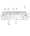
図1(a)は本発明の実施形態1による振動センサ11の構造を示す平面図、図1(b)はその断面図である。この振動センサ11は、例えば半導体マイクロフォンや超音波センサ等の音響センサ、薄膜フィルタ等に用いられるものである。振動センサ11は、Si基板12と、素子薄膜13(ダイアフラム)とを有している。このSi基板12は(100)面基板である。Si基板12は、裏面側からエッチングすることによって表裏に貫通し、さらに縦横の各方向の辺が(110)方向に沿った矩形の貫通孔14を設けられている。貫通孔14は、表面側と裏面側とに(111)面又はそれと等価な結晶面による傾斜面15、17が形成され、両傾斜面15、17間には垂直面16が形成されている。ここで、垂直面16は実際には(110)面、(311)面、(411)面などの複数の結晶面で構成されているが、簡易的に垂直面で示している。従って、貫通孔14の縁における基板断面は、表裏でテーパーの付いた形状となっている。(Embodiment 1)
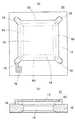
FIG. 1A is a plan view showing the structure of a
素子薄膜13は、前記貫通孔14の表面側開口を覆うようにしてSi基板12の上面に配置されており、下面の全周を保持部18によってSi基板12上面に固定されている。保持部18により貫通孔14の表面側開口(あるいは、Si基板12の表面であった面)と素子薄膜13の裏面との間に狭い隙間19が形成されている。 The element
このような構造の振動センサ11であると、裏面側からSi基板12をエッチングして貫通孔14を形成しているにも拘わらず、貫通孔14の表面側開口に比較して裏面側開口の面積があまり大きくならない。従って、最初の従来例のように貫通孔14のためにSi基板12の面積が大きくならない。Si基板12は素子薄膜13及び必要であれば回路部品を実装できるだけの大きさがあれば足り、振動センサ11を小型化することができる。 In the case of the
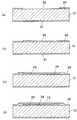
次に、図2(a)〜(d)、図3(a)〜(d)及び図4(a)〜(c)により、上記振動センサ11の製造工程を説明する。ただし、振動センサ11はウエハ上で多数個一度に製造されるが、以下の説明では、1個の振動センサ11だけを図示して説明する。 Next, the manufacturing process of the
まず、図2(a)に示すように、(100)面Si基板12の表面及び裏面に熱酸化法などによってSiO2からなる保護膜20、21を成膜する。ついで、Si基板12の表面において、上記隙間19を形成しようとする領域の保護膜20をフォトリソグラフィ技術を用いて部分的に除去し、矩形状のエッチング窓22を開口する。First, as shown in FIG. 2A,
保護膜20の上からSi基板12の表面に多結晶シリコン薄膜を成膜し、フォトリソグラフィ技術を用いて保護膜20の上に乗っている多結晶シリコン薄膜を除去する。これにより、エッチング窓22内においてSi基板12の表面に多結晶シリコン薄膜からなる矩形状の犠牲層23を成膜する。このときの状態を図2(b)に示す。 A polycrystalline silicon thin film is formed on the surface of the
次に、犠牲層23の上からSi基板12の表面に、SiO2よりなる保護膜24を成膜し、図2(c)に示すように、犠牲層23を保護膜24で覆い隠す。Next, a
ついで、保護膜24の上に多結晶シリコン薄膜を形成し、フォトリソグラフィ技術を用いて多結晶シリコン薄膜の不要部分を除去し、図2(d)に示すように、保護膜24の上に多結晶シリコン薄膜からなる素子薄膜13を形成する。さらに、図3(a)に示すように、素子薄膜13の上にSiO2よりなる矩形状の保護膜25を成膜し、素子薄膜13を保護膜25で覆い隠す。Next, a polycrystalline silicon thin film is formed on the
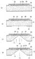
この後、図3(b)に示すように、Si基板12の裏面において保護膜21の一部をフォトリソグラフィ技術を用いて部分的に除去し、保護膜21に裏面エッチング窓26を矩形状に開口する。裏面エッチング窓26は、裏面エッチング窓26から開始した結晶異方性エッチングがSi基板12の表面に達するだけの大きさがあればよく、例えば厚みが400μmのSi基板12であれば、1辺が570μm程度の比較的小さな裏面エッチング窓26で十分である。なお、犠牲層23の縦横サイズの大きさは必要な素子薄膜13の縦横サイズの大きさで決まり、例えば一辺が650μm程度である。 Thereafter, as shown in FIG. 3B, a part of the
裏面エッチング窓26を開口したら、TMAHやKOH、EDP等のエッチャント(以下、TMAH等のエッチャントという。)に浸漬して裏面エッチング窓26からエッチングを行なう。TMAH等のエッチャントは、Siに対しては結晶異方性エッチングを行なうので、Si基板12の裏面では、(111)面及びそれに等価な結晶面(傾斜面17)に沿ってエッチングが進み、Si基板12の裏面に角錐台状をした貫通孔14が形成される。 When the back
こうして貫通孔14がSi基板12の表面に達すると、図3(c)に示すように、貫通孔14から犠牲層23が露出する。SiO2からなる保護膜20、21、24、25は、TMAH等のエッチャントではエッチングされないが、多結晶シリコンからなる犠牲層23はTMAH等のエッチャントにより等方性エッチングされる。よって、貫通孔14内に犠牲層23が露出すると、図3(d)に示すように、犠牲層23は貫通孔14内に露出した部分から周囲へとエッチングされていき、保護膜24とSi基板12の表面との間に隙間19が生じる。When the through
この状態では、素子薄膜13及び保護膜24、25は、隙間19によりSi基板12の表面から浮いているため、薄膜として機能させることができる。しかし、この隙間19は厚みの薄い空間であるので、素子薄膜13及び保護膜24、25が振動するとダンピング効果が起こり、周波数の高い帯域の振動特性を劣化させたり、機械的ノイズの原因となったりし、また素子薄膜13及び保護膜24、25がSi基板12へスティック(貼り付き)しやすくなる。これらを防止するため、素子薄膜13の下方においてSi基板12のエッチングをさらに継続する。 In this state, the element
なお、隙間19(犠牲層23)の厚みは、厚い方がそのエッチング速度は速くなるが、厚すぎると犠牲層23の成膜時間が多くかかったり、保護膜24の被膜性が悪くなったりするため、それら加味して設計し、例えば1μm程度とする。一方、素子薄膜13の厚みは振動センサ11の感度と強度のトレードオフを考慮して設計し、例えば1μm程度とする。 Note that the thicker the gap 19 (sacrificial layer 23), the faster the etching rate. However, if the thickness is too thick, the
保護膜24とSi基板12の表面との間に隙間19が生じると、エッチャントは隙間19に浸入し、Si基板12を表面側から結晶異方性エッチングする。この異方性エッチングでは、図4(a)において矢印で示した方向にエッチングが進み、貫通孔14内に傾斜面15が形成される。さらに、貫通孔14の縁の尖端部分ではエッチング速度が大きいので、貫通孔14の内周面は角が取れて垂直面16が形成され、貫通孔14はドーナツの孔のような形状にエッチングされる。こうして、図4(b)のように犠牲層23が完全にエッチング除去された時点でSi基板12をエッチャントから引き上げる。 When the
Si基板12を洗浄した後、HF水溶液などでSiO2からなる保護膜20、21、24、25をエッチングし、図4(c)のように保護膜20、24の一部による保持部18だけが残った時点でエッチングを終了し、洗浄及び乾燥を行なって振動センサ11を完成する。After cleaning the
このようにして振動センサ11を製作すれば、Si基板12の裏面側からのエッチングのみで、裏面側における広がりの小さな貫通孔14を開口することができ、振動センサ11を小型化することができる。また、裏面側からのみのエッチングで貫通孔14を開口することができるので、素子薄膜13にエッチングホールを開口する必要が無く、振動センサ11における素子薄膜13の物理的特性を変化させたり、素子薄膜13の強度を低下させたりする恐れが小さくなる。 If the
また、貫通孔14の裏面側の開口面積は保護膜21に明けた裏面エッチング窓26の大きさによって決まり、貫通孔14の表面側の開口面積は犠牲層23の大きさによって決まるので、上記のような製造方法によれば、貫通孔14の開口面積を精度良くコントロールすることができる。 Further, the opening area on the back surface side of the through
なお、上記実施形態では、犠牲層23を多結晶シリコンによって成膜したが、アモルファスシリコンを用いてもよい。 In the above embodiment, the
(実施形態2)
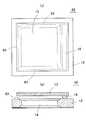
図5(a)は本発明の実施形態2による振動センサ31を示す平面図、図5(b)はその断面図である。この振動センサ31では、貫通孔14の上面を覆うようにしてSi基板12の上に多結晶シリコンからなる素子薄膜13が形成されている。素子薄膜13は、Si基板12の上面で保持部18によって外周部下面を支持されていてSi基板12の上面から浮かされており、保持部18で囲まれた領域が変形可能となっている。(Embodiment 2)
FIG. 5A is a plan view showing a
図6(a)〜(d)及び図7(a)〜(d)は、この振動センサ31の製造工程を説明する断面図である。以下、図6(a)〜(d)及び図7(a)〜(d)に従って、振動センサ31の製造工程を説明する。 6A to 6D and FIGS. 7A to 7D are cross-sectional views for explaining the manufacturing process of the
まず、Si基板12の上面にSiO2薄膜を形成した後、フォトリソグラフィ技術を用いてSiO2薄膜の不要部分を除去し、図6(a)に示すように、Si基板12の上面から素子薄膜13を浮かそうとする領域にのみSiO2薄膜からなる犠牲層32を形成する。First, after forming a SiO2 thin film on the upper surface of the
次に、犠牲層32の上からSi基板12の表面に、SiNからなる保護膜34を成膜し、図6(b)に示すように、犠牲層32を保護膜34で覆い隠す。ついで、図6(c)に示すように、保護膜34の表面に多結晶シリコンからなる素子薄膜13を成膜する。 Next, a
さらに、図6(d)に示すように、素子薄膜13の上から保護膜34の表面にSiNよりなる保護膜35を成膜し、素子薄膜13を保護膜35で覆い隠す。また、Si基板12の裏面にSiO2以外の材料からなる保護膜33を成膜する。このとき、保護膜33をSiN薄膜によって形成すれば、保護膜34もしくは保護膜35と保護膜33とを同一工程により一度に形成することができる。Si基板12の裏面に保護膜33が成膜されたら、図6(d)に示すように保護膜33の一部をフォトリソグラフィ技術を用いて矩形状に開口し、裏面エッチング窓26を形成する。裏面エッチング窓26は、裏面エッチング窓26からの結晶異方性エッチングがSi基板12の表面に達するだけの大きさがあればよい。Further, as shown in FIG. 6D, a
裏面エッチング窓26が開口されたら、TMAH等のエッチャントにSi基板12を浸漬して裏面エッチング窓26からSi基板12をエッチングし、Si基板12に貫通孔14を設ける。TMAH等のエッチャントは、Siに対しては結晶異方性エッチングとなるので、Si基板12の裏面では、(111)面及びそれに等価な結晶面に沿ってエッチングが進み、ついには図7(a)に示すように、貫通孔14がSi基板12の表面に達して犠牲層32が貫通孔14内に露出する。 When the back
SiO2からなる犠牲層32はTMAH等のエッチャントではエッチングされないので、犠牲層32が露出したら当該エッチング処理を終了し、Si基板12を洗浄する。Since the
ついで、Si基板12をHF水溶液に浸漬する。HF水溶液はSi基板12を侵さないが、SiO2を等方的にエッチングするので、Si基板12の裏面側から貫通孔14内に入ったHF水溶液により、犠牲層32が露出部分から周囲へとエッチングされていき、図7(b)に示すように、素子薄膜13とSi基板12の表面との間に隙間19が生じる。Next, the
犠牲層32がエッチングにより完全に除去されたら、Si基板12を洗浄した後、再びTMAH等のエッチャントに浸漬する。このエッチャントは、隙間19に浸入してSi基板12を表面側から結晶異方性エッチングする。その結果、実施形態1の場合と同様に、貫通孔14の内周面でSi基板12の角が取れて傾斜面15と垂直面16が形成され、貫通孔14がドーナツの孔のような形状にエッチングされる。こうして、図7(c)のように所望の貫通孔14が形成されたらSi基板12をエッチャントから引き上げ、洗浄及び乾燥を行なう。最後に図7(d)に示すように、SiNからなる保護膜33、34、35を、加熱した燐酸水溶液などにより除去し、振動センサ31を完成する。 After the
このようにして振動センサ31を製作すれば、Si基板12の裏面側からのエッチングのみで、裏面側における広がりの小さな貫通孔14を開口することができ、振動センサ31を小型化することができる。また、裏面側からのみのエッチングで貫通孔14を開口することができるので、素子薄膜13にエッチングホールを開口する必要が無く、振動センサ31における素子薄膜13の物理的特性を変化させたり、素子薄膜13の強度を低下させたりする恐れが小さくなる。 If the
また、貫通孔14の裏面側の開口面積は保護膜33に明けた裏面エッチング窓26の大きさによって決まり、貫通孔14の表面側の開口面積は犠牲層32の大きさによって決まるので、上記のような製造方法によれば、貫通孔14の開口面積を精度良くコントロールすることができる。 Further, the opening area on the back surface side of the through
さらに、貫通孔の結晶異方性エッチングの工程と犠牲層をエッチングする工程とでエッチャントを切り替えているので、それぞれの工程でエッチャントを選択する際の制約が少なくなる。また、結晶異方性エッチングから等方性エッチングへと連続して移行しないために、各エッチング工程で歩留まり検査などの工程管理をすることができるという利点もある。 Furthermore, since the etchant is switched between the step of crystal anisotropic etching of the through hole and the step of etching the sacrificial layer, there are less restrictions on selecting the etchant in each step. In addition, since there is no continuous transition from crystal anisotropic etching to isotropic etching, there is also an advantage that process management such as yield inspection can be performed in each etching process.
また、実施形態1の場合には、結晶異方性エッチングと等方性エッチングとを同一のエッチャントによって行なったので、結晶異方性エッチングと等方性エッチングとを同一装置内で連続して行え、作業効率が高かった。これに対し、実施形態2の場合には、結晶異方性エッチングと等方性エッチングとを別工程としているので、結晶異方性エッチングの手段と等方性エッチングの手段の制約が少なくなり、例えば等方性エッチングは水溶液以外の腐食性のガスなどを用いた化学的エッチングとすることもできる。 In the case of the first embodiment, since the crystal anisotropic etching and the isotropic etching are performed by the same etchant, the crystal anisotropic etching and the isotropic etching can be continuously performed in the same apparatus. The work efficiency was high. On the other hand, in the case of the embodiment 2, since the crystal anisotropic etching and the isotropic etching are separate processes, the restrictions on the means for crystal anisotropic etching and the means for isotropic etching are reduced. For example, the isotropic etching may be chemical etching using a corrosive gas other than an aqueous solution.
(実施形態3)
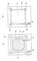
図8(a)は本発明の実施形態3による振動センサ41の構造を示す平面図、図8(b)は図8(a)のX−X線断面図である。この振動センサ41は、素子薄膜13にしわ(皺)構造やストッパ43などの機能部分を設けたものである。(Embodiment 3)
FIG. 8A is a plan view showing the structure of the
素子薄膜13のしわ構造は、四角環状をした2つの屈曲部42によって構成されている。各屈曲部42は、その断面が素子薄膜13の上面側へ突出するように屈曲している。このように素子薄膜13にしわ構造を形成すれば、素子薄膜13の変位が大きくなったり、応力による撓みが少なくなることは、"The fabrication and use of micromachined corrugated silicon diaphragms"(J. H. Jerman, Sensors and Actuators A21-A23 pp.998-992, 1992)に報告されている。 The wrinkle structure of the element
ストッパ43は、素子薄膜13の表面が丸い突起状に突出したものである。静電容量型の振動センサ(例えば、後述のマイクロフォンなど)の場合には、素子薄膜13が可動電極となり、素子薄膜13の上面に対向電極(固定電極)が配置される。静電容量型の振動センサの場合には、素子薄膜13の上面にストッパ43を設けておけば、素子薄膜13が大きく変形した場合でも、ストッパ43が固定電極に当接することにより、振動センサ41の電荷帯電に起因する静電力や、水分固着に起因する毛細管力などによって素子薄膜13が対向電極に吸着されるのを防ぐことができる。 The
図9(a)(b)、図10(a)〜(d)、図11(a)(b)、図12(a)(b)、図13(a)(b)は、上記振動センサ41の製造工程を説明する図である。以下、図9〜図13に従って振動センサ41の製造工程を説明する。まず、図9(a)(b)に示すように、Si基板12の表面に多結晶シリコン薄膜からなる犠牲層を所定パターンに形成する。この犠牲層は、中央部に位置する四角形の犠牲層44a、屈曲部42の形成領域に形成された四角環状の犠牲層44b、44c、犠牲層44a〜44cをつなぐ線状の犠牲層44d、ストッパ43の形成領域に形成された犠牲層44eからなる。 FIGS. 9A and 9B, FIGS. 10A to 10D, FIGS. 11A and 11B, FIGS. 12A and 12B, and FIGS. 13A and 13B are the vibration sensors. It is a figure explaining the manufacturing process of 41. FIG. Hereinafter, the manufacturing process of the
ついで、図10(a)に示すように、犠牲層44a〜44eの上からSi基板12の表面をSiO2からなる保護膜45で覆い、Si基板12の裏面にもSiO2からなる保護膜46を形成する。このとき保護膜45は、各犠牲層44a〜44eの上に成膜されるので、各犠牲層44a〜44eの部分では保護膜45は上に突出している。Next, as shown in FIG. 10A, the surface of the
図10(b)に示すように、保護膜45の上に多結晶シリコン薄膜からなる素子薄膜13を形成する。素子薄膜13は、各犠牲層44a〜44eの領域では、保護膜45を介して各犠牲層44a〜44eによって持ち上げられるので、犠牲層44b、44cの上で屈曲部42が形成され、犠牲層44eの上にストッパ43が形成される。なお、犠牲層44a及び44dの上でも素子薄膜13が上に膨らんで突部47、48が形成される。 As shown in FIG. 10B, an element
さらに、図10(c)に示すように、素子薄膜13の上から保護膜45の表面にSiO2からなる保護膜49を成膜して保護膜49で素子薄膜13を覆い隠し、Si基板12の裏面の保護膜46に裏面エッチング窓50を開口する。Further, as shown in FIG. 10 (c), a
この後、Si基板12をTMAH等のエッチャントに浸漬して裏面エッチング窓50から結晶異方性エッチングを行ない、Si基板12の裏面に角錐台状をした貫通孔14を形成する。貫通孔14は、Si基板12下面におけるエッチングが裏面エッチング窓50の縁に達すると停止する。 Thereafter, the
貫通孔14がSi基板12の表面に達すると、図10(d)に示すように、犠牲層44aが貫通孔14に露出する。犠牲層44aが露出すると、犠牲層44aはTMAH等のエッチャントで等方的エッチングされる。こうして犠牲層44aから始まった等方的エッチングは、図11(a)に細線矢印で示すように、犠牲層44a→犠牲層44d→犠牲層44b→犠牲層44cというように進んでいく。そして、犠牲層44a〜44dがエッチングされた後の隙間にエッチャントが浸入すると、図11(a)(b)及び図12(a)(図12(a)はSi基板12の表面を表わす。)に太線矢印で示すように、犠牲層44a〜44dの除去された跡の隙間51a〜51dのエッジ部からSi基板12の結晶異方性エッチングが進み、Si基板12の表面側からも貫通孔14のエッチングが行なわれる。 When the through
この結果、犠牲層44cの外周よりも内側の領域でSi基板12の上面がエッチングされ、Si基板12には表面側と裏面側とからエッチングされた貫通孔14ができる。また、この際に犠牲層44eをエッチングにより除去される。こうして、貫通孔14が完全に形成された時点でSi基板12をエッチャントから引き上げる。 As a result, the upper surface of the
Si基板12を洗浄した後、HF水溶液などでSiO2からなる保護膜45、49をエッチング除去し、図13(a)(b)に示すように、素子薄膜13の四隅に保護膜45による保持部18だけが残った時点でエッチングを終了し、洗浄及び乾燥を行なって振動センサ41を完成する。After the
この実施形態でも、Si基板12の裏面側からのエッチングのみで、裏面側における広がりの小さな貫通孔14を開口することができ、振動センサ41を小型化することができる。また、裏面側からのみのエッチングで貫通孔14を開口することができるので、素子薄膜13にエッチングホールを開口する必要が無く、振動センサ41における素子薄膜13の物理的特性を変化させたり、素子薄膜13の強度を低下させたりする恐れが小さくなる。また、同じ工程により素子薄膜13にしわ構造やストッパ等を容易に形成することができる。 Also in this embodiment, the through-
(実施形態4)
図14(a)は本発明の実施形態4による振動センサ61の構造を示す平面図、図14(b)はその断面図である。実施形態1の振動センサ11では、素子薄膜13の下面全周に保持部18を形成していたが、実施形態4の振動センサ61では素子薄膜13のコーナー部(四隅)にのみ保持部18を形成している。実施形態4の振動センサ61では、素子薄膜13のコーナー部にのみ保持部18を設けているので、4辺において素子薄膜13の保持部18間のベントホール63を通じて素子薄膜13の上面側と下面側とが連通している。(Embodiment 4)
FIG. 14A is a plan view showing a structure of a
図15(a)は本発明の実施形態4の別な振動センサ62の構造を示す平面図、図15(b)はその断面図である。この振動センサ62では、素子薄膜13の一辺にのみ保持部18を形成している。この振動センサ62では、素子薄膜13が保持部18によって片持ち状に支持されているので、素子薄膜13の上面側と下面側とが3辺のベントホール63を通して連通している。 FIG. 15A is a plan view showing the structure of another
振動センサ61、62のように部分的に保持部18を形成するためには、保持部18を形成しようとする部分で保護膜の幅を広くしておいたり、エッチャント投入位置からの距離(エッチング開始位置から終了位置までの距離)を大きくしておいたりして、エッチング時間を管理することで一部保護膜を除去し一部保護膜を残してやれば、残った保護膜によって保持部18を形成することができる。例えば、振動センサ61では、中心から遠い位置に保持部18が形成されている。また、振動センサ62では、1辺の保護膜の幅を他3辺の保護膜の幅よりも大きくしておいてエッチング後に残るようにしている。 In order to partially form the holding
振動センサ61、62のような構造は、マイクロフォン(音響センサ)としての用途に望ましいものである。すなわち、振動センサ61、62では、素子薄膜13は一部分を固定されているだけであるので、素子薄膜13が柔軟になって弾性変形し易くなる。従って、動的な圧力差を検知するマイクロフォンなどとして用いるのに適している。 Structures such as the
特に素子薄膜13が矩形の場合に、振動センサ61のように素子薄膜13の4つのコーナー部のみを固定すると、素子薄膜13が柔軟なバネとなる。さらにこの四隅のみの固定方法によると、素子薄膜13の大部分が平行平板のように変形するために、静電容量式マイクロフォンの感度が飛躍的に向上する。 In particular, when the element
なお、素子薄膜13の四隅の固定部分は、変形による外部からの応力が集中しないよう、対角線方向に延伸した形状とするのがよい。またこの延伸した部位に電極パッド73を接続するようにすれば、素子薄膜13の振動を阻害せずに素子薄膜13から電極を取り出すことができる。 The fixed portions at the four corners of the element
また、保持部18の内部応力は素子薄膜13の振動特性に影響を与えるため、保持部18の内部応力を制御することで素子薄膜13の振動特性を変化させられる。例えば、素子薄膜13が強い引張応力の場合には、保持部18を圧縮応力を持った酸化膜とすることで素子薄膜13の引張応力を弱め、感度を向上させることができる。 Further, since the internal stress of the holding
また、振動センサ61、62のような構造によれば、Si基板12の表面と素子薄膜13との間で通気性を有するので、素子薄膜13の両面で静的な圧力差を無くすことができベントホールの機能を持たせることができる。 Further, according to the structure such as the
米国特許第5,452,268号などでは、音響抵抗を高めるために平面方向のベントホールの幅を短くしている。しかし、ベントホールの幅を狭くするのにはプロセスルール的に限界があり、あまり効果を期待することができない。 In US Pat. No. 5,452,268, etc., the width of the vent hole in the planar direction is shortened in order to increase acoustic resistance. However, there is a limit in the process rule to narrow the width of the vent hole, and the effect cannot be expected so much.
ベントホールの抵抗成分Rvは、
Rv=(8・μ・t・a2)/(Sv2) …(数1)
で表わされる。但し、μはベントホールの摩擦損失係数、tはベントホールの通気方向の長さ、aはダイアフラムの面積、Svはベントホールの断面積である。また、マイクロフォンのロールオフ周波数fL(感度の低下する限界周波数)は、
1/fL=2π・Rv(Cbc+Csp) …(数2)
で表わされる。但し、但し、Rvは上式の抵抗成分、Cbcは貫通孔14の音響コンプライアンス、Cspは素子薄膜13のスティフネス定数である。The resistance component Rv of the vent hole is
Rv = (8 · μ · t · a2 ) / (Sv2 ) (Equation 1)
It is represented by Where μ is the friction loss coefficient of the vent hole, t is the length of the vent hole in the ventilation direction, a is the area of the diaphragm, and Sv is the sectional area of the vent hole. The roll-off frequency fL of the microphone (the limit frequency at which the sensitivity decreases) is
1 / fL = 2π · Rv (Cbc + Csp) (Expression 2)
It is represented by However, Rv is the resistance component of the above equation, Cbc is the acoustic compliance of the through
振動センサ61、62では、図16に示すように、Si基板12の上面と素子薄膜13との間のベントホール63の長さtを長くとることができる。よって振動センサ61、62では、上記(数1)から分かるように、ベントホール63の長さtを長くとることによって音響抵抗を非常に高くすることができ、また上記(数2)から分かるように、振動センサ61、62の低周波特性を改善することができるので、マイクロフォンとして好ましい特性を得ることができる。 In the
また、貫通孔14の音響コンプライアンス(バックチャンバーの音響コンプライアンス)Ccavは、
Ccav=Vbc/(ρc2・Sbc) …(数3)
で表わされる。但し、Vbcは貫通孔14の体積(バックチャンバー体積)、ρc2は空気の体積弾性率、Sbcは貫通孔14の開口部の面積である。The acoustic compliance (acoustic compliance of the back chamber) Ccav of the through
Ccav = Vbc / (ρc2 · Sbc) (Equation 3)
It is represented by Where Vbc is the volume of the through hole 14 (back chamber volume), ρc2 is the volume modulus of air, and Sbc is the area of the opening of the through
振動センサ61、62では、Si基板12の表裏両面からエッチングすることにより、体積に比べて開口面積の小さな貫通孔14を形成することができるので、上記(数3)から分かるように、貫通孔14の音響コンプライアンスを大きくすることができ、ベントホール63を開口していても感度が下がりにくくできる。 In the
また、図17(a)のように、貫通孔14がその中央部が内側へ突出するように結晶異方性エッチングされた後、さらにエッチングを継続すると、図17(b)のような状態を経て最終的に図17(c)のような状態までエッチングが進み、(111)面又はそれに等価な結晶面が現れたところで貫通孔14のエッチングが停止する。従って、図17(c)のような状態までエッチングすれば、貫通孔14の体積がより大きくなり、音響コンプライアンスCcavをより大きくできる。あるいは、図17(a)の状態から図17(c)の状態へエッチングする際に、エッチング時間を制御することにより適切な貫通孔14の体積と振動センサのサイズを得ることができる。 Further, as shown in FIG. 17A, after the crystal anisotropic etching is performed so that the central portion of the through
また、図17(c)の状態は、結晶異方性エッチングの最終形態であり、表面と裏面の開口部の大きさと相対位置によってバックチャンバーの形状が決まる。最終形態となった場合には、それ以上エッチング時間を長くしてもバックチャンバー(貫通孔14)の形状はほぼ一定に保たれるため、プロセス安定性がよく、歩留まりが高くなる利点がある。 The state shown in FIG. 17C is the final form of crystal anisotropic etching, and the shape of the back chamber is determined by the size and relative position of the openings on the front and back surfaces. In the case of the final form, the shape of the back chamber (through hole 14) can be kept almost constant even if the etching time is further increased, so that there is an advantage that the process stability is good and the yield is high.
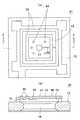
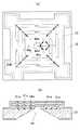
つぎに、上記のような構造の振動センサ61を利用して構成した静電容量型のマイクロフォン71の構造とその製造方法を説明する。図18(a)はマイクロフォン71の平面図、図18(b)はバックプレート72を取り除いた状態におけるマイクロフォン71(つまり、振動センサ61)の平面図、図19はマイクロフォン71の断面図である。このマイクロフォン71は、素子薄膜13を覆うようにして振動センサ61の上にバックプレート72を固定している。バックプレート72は下面に凹部を有するキャップ状をしており、凹部内に素子薄膜13を納めるようにしてSi基板12の表面に固定されている。また、バックプレート72の下面と素子薄膜13との間には、素子薄膜13の振動を妨げない程度の隙間が形成されている。 Next, the structure of a
バックプレート72の上面には金属電極73が設けられている。金属電極73は、図18に示す通りバックプレートの全面に設けられているのではなく、バックプレート72の一部分、特に素子薄膜13の比較的振幅が大きい部分に対向する部分に設けられている。これは、寄生容量を少なくし、静電容量型のマイクロフォン71の特性を向上させるためである。本実施形態のように素子薄膜13が四隅で固定されている場合には、金属電極73の形状を図18(a)に示すようにほぼ八角形とすると、寄生容量を少なくし、かつ限られた領域を有効に活用することができる。金属電極73及びバックプレート72には複数のアコースティックホール74、75を開口している。よって、上方からの音響振動は、金属電極73及びバックプレート72のアコースティックホール74、75を通過して素子薄膜13に達し、素子薄膜13を振動させる。多結晶シリコンからなる素子薄膜13(可動電極)は導電性を有しており、素子薄膜13が振動すると素子薄膜13と金属電極73(固定電極)との間の静電容量が変化するので、これらを素子薄膜13側の電極パッド76、バックプレート72側の電極パッド77を通じて外部へ電気信号として取り出し、この静電容量の変化を検出することによって音響振動を検知できる。 A
次に、マイクロフォン71の製造工程を図20(a)〜(d)及び図21(a)〜(d)により説明する。まず、図20(a)に示すように、Si基板12の表面に保護膜20、犠牲層23、保護膜24、素子薄膜13、保護膜25を順次積層し、またSi基板12の裏面に保護膜21を成膜する。これは実施形態1の図3(a)と同じ構造であって、実施形態1の図2(a)〜図2(d)と同じ工程を経て作製される。 Next, the manufacturing process of the
ついで、図20(b)に示すように、保護膜25の表面から保護膜24及び25の外周面に掛けてSiN膜を成膜し、SiN膜によってバックプレート72を形成する。その後、図20(c)に示すように、エッチングによってバックプレート72にアコースティックホール75を開口する。この際に、図20には記載していないが、電極取り出し部分のSiN膜もエッチングしておく。ついで、図20(d)に示すように、バックプレート72の表面にCr膜を成膜し、その上にAuを成膜してAu/Cr膜を得た後、Au/Cr膜を所定形状にエッチングして金属電極73及び電極パッド76、77を作製する。 Next, as shown in FIG. 20B, a SiN film is formed from the surface of the
次に、フォトリソグラフィ技術を用いて裏面の保護膜21に裏面エッチング窓26を開口する。裏面エッチング窓26の大きさは、厚み400μmの(100)面Si基板12であれば、1辺570μm程度で十分である。裏面エッチング窓26が開口されたら、Si基板12をTMAH等のエッチャントに浸漬して裏面側からSi基板12を結晶異方性エッチングし、Si基板12に貫通孔14を開口する。この状態を図21(a)に示す。 Next, a back
図21(a)に示すように、貫通孔14内に犠牲層23が露出すると、多結晶シリコンの犠牲層23がTMAH等のエッチャントによって等方性エッチングされ、図21(b)に示すように、Si基板12の表面に隙間19ができる。隙間19ができると、この隙間19にTMAH等のエッチャントが浸入してSi基板12を表面側からもエッチングし、さらに水平方向にもエッチングが進むので、貫通孔14の縁は図21(c)に示すように表裏にテーパーのついた断面形状となる。 As shown in FIG. 21 (a), when the
所望の貫通孔14の形状が得られたらSi基板12をエッチャントから引き上げる。そして、素子薄膜13を保護している保護膜21、24、25をHF水溶液などでエッチングし、バックプレート72の下面の保護膜20と保持部18を残して除去する。このとき、保護膜25は、主にアコースティックホール74、75から入り込んだHF水溶液でエッチングされる。よって、アコースティックホール74、75の配置間隔は、図18(a)に示される通り、エッチングが均等になされるようにほぼ等間隔とすることが望ましい。ここで配置間隔を小さくするとエッチング時間を短縮できるが、その分アコースティックホール74、75の数が増え、電極面積が小さくなって感度が減少してしまう。また、アコースティックホールの配置間隔は保持部18の大きさにも関係している。すなわち配置間隔が大き過ぎると、エッチング時間が長くなって保持部18が全てエッチングにされてしまう。これらのことを加味し、アコースティックホール74、75の間隔は50μmとした。保持部18は素子薄膜13のコーナー部にのみ形成され、保持部18間にはベントホール63が開口される。こうして、図20(d)のような構造のマイクロフォン71を完成する。 When the desired shape of the through
このようにしてマイクロフォン71を製作することにより、Si基板12の表面側と裏面側とから貫通孔14をエッチングでき、貫通孔14の傾斜面による面積ロスを少なくでき、マイクロフォン71の小型化を図ることができる。しかも、結晶異方性エッチングと等方性エッチングとを組み合わせることで、裏面側からエッチングを開始して表面側と裏面側からSi基板12を結晶異方性エッチングして貫通孔14を開口させることができる。よって、簡略な工程により貫通孔14を開口することができ、低コスト化と高量産性とを両立できる。また、素子薄膜13にエッチングホールを開口する必要がないので、素子薄膜13の強度を低下させたり、振動特性を劣化させたりする恐れも少なくなる。 By manufacturing the
さらに、素子薄膜13を保持部18で部分的に支持しているので、素子薄膜13が振動しやすくなってマイクロフォン71の感度が向上し、また保持部18間で素子薄膜13とSi基板12の隙間に長いベントホール63を形成できるので、マイクロフォン71の音響抵抗を高くして低周波特性を改善できる。さらに、貫通孔14の体積を大きくできるので、音響コンプライアンスを大きくしてマイクロフォン71の特性を改善できる。 Furthermore, since the element
なお、上記各実施形態においては、基板として(100)面Si基板を用いた場合について説明したが、(110)面Si基板などを用いてもよい。 In each of the above embodiments, the case where the (100) plane Si substrate is used as the substrate has been described, but a (110) plane Si substrate or the like may be used.
11 振動センサ
12 Si基板
13 素子薄膜
14 貫通孔
18 保持部
20、21 保護膜
22 エッチング窓
23 犠牲層
24、25 保護膜
26 裏面エッチング窓
31 振動センサ
32 犠牲層
33 保護膜
41 振動センサ
42 屈曲部
43 ストッパ
44a〜44e 犠牲層
45、46 保護膜
49 保護膜
50 裏面エッチング窓
71 マイクロフォン
72 バックプレート
73 金属電極
74 アコースティックホール
75 アコースティックホールDESCRIPTION OF
Claims (11)
Translated fromJapanese前記犠牲層および前記犠牲層の周囲の前記半導体基板の表面の上に、前記エッチャントに対して耐性を有する材料で素子薄膜保護膜を形成する工程と、
前記犠牲層の上方に、単結晶シリコン、多結晶シリコンもしくはアモルファスシリコンからなる素子薄膜を形成する工程と、
前記半導体基板の裏面に形成された、前記半導体基板をエッチングするためのエッチャントに対して耐性を有する裏面保護膜に裏面エッチング窓を開口する工程と、
前記裏面エッチング窓からエッチャントを適用して前記半導体基板を裏面側から結晶異方性エッチングすることにより、当該エッチングが前記半導体基板の表面に達したときに前記エッチャントによって前記犠牲層を等方性エッチングさせ、前記犠牲層がエッチング除去された跡の空間に広がった前記エッチャントによって前記半導体基板を表面側から結晶異方性エッチングさせ、前記半導体基板に貫通孔を形成する工程と、
前記素子薄膜保護膜を一部を残して除去し、残された前記素子薄膜保護膜によって前記半導体基板の上面で前記素子薄膜を支持するための保持部を設ける工程と
を有することを特徴とする振動センサの製造方法。Forming a sacrificial layer with a material that is isotropically etched by an etchant for etching the semiconductor substrate on a part of the surface of the semiconductor substrate made of single crystal silicon;
Forming a device thin film protective film on the sacrificial layer and a surface of the semiconductor substrate around the sacrificial layer with a material having resistance to the etchant;
Forming a device thin film made of single crystal silicon, polycrystalline silicon or amorphous silicon above the sacrificial layer;
Opening a back surface etching window in a back surface protection film having resistance to an etchant for etching the semiconductor substrate formed on the back surface of the semiconductor substrate;
An isotropic etch of the sacrificial layer with the etchant when the etch reaches the surface of the semiconductor substrate by applying an etchant from the back-side etch window and subjecting the semiconductor substrate to crystal anisotropic etching from the back side. The semiconductor substrate is crystal-anisotropically etched from the surface side by the etchant spreading in the space where the sacrificial layer has been etched away, and a through hole is formed in the semiconductor substrate;
Removing the element thin film protective film except for a part thereof, and providing a holding portion for supporting the element thin film on the upper surface of the semiconductor substrate by the remaining element thin film protective film. A method for manufacturing a vibration sensor.
前記犠牲層および前記犠牲層の周囲の前記半導体基板の表面の上に、前記第1のエッチャントに対して耐性を有する材料で素子薄膜保護膜を形成する工程と、
前記犠牲層の上方に、単結晶シリコン、多結晶シリコンもしくはアモルファスシリコンからなる素子薄膜を形成する工程と、
前記半導体基板の裏面に形成された、前記半導体基板をエッチングするためのエッチャントに対して耐性を有する裏面保護膜に裏面エッチング窓を開口する工程と、
前記裏面エッチング窓から第1のエッチャントを適用して前記半導体基板を裏面側から結晶異方性エッチングする工程と、
前記第1のエッチャントによるエッチングが前記半導体基板の表面に達した後、前記半導体基板の裏面側から第2のエッチャントを適用することによって前記犠牲層を等方性エッチングする工程と、
前記犠牲層がエッチング除去された後、前記犠牲層がエッチング除去された跡の空間に前記半導体基板の裏面側から再び前記第1のエッチャントを適用することによって前記半導体基板を表面側から結晶異方性エッチングし、前記半導体基板に貫通孔を形成する工程と、
前記素子薄膜保護膜を一部を残して除去し、残された前記素子薄膜保護膜によって前記半導体基板の上面で前記素子薄膜を支持するための保持部を設ける工程と
を有することを特徴とする振動センサの製造方法。Forming a sacrificial layer with a material resistant to a first etchant for etching the semiconductor substrate on a part of the surface of the semiconductor substrate made of single crystal silicon;
Forming an element thin film protective film with a material having resistance to the first etchant on the sacrificial layer and the surface of the semiconductor substrate around the sacrificial layer;
Forming a device thin film made of single crystal silicon, polycrystalline silicon or amorphous silicon above the sacrificial layer;
Opening a back surface etching window in a back surface protection film having resistance to an etchant for etching the semiconductor substrate formed on the back surface of the semiconductor substrate;
Applying a first etchant from the back surface etching window to anisotropically etch the semiconductor substrate from the back surface side;
After the etching by the first etchant reaches the surface of the semiconductor substrate, isotropically etching the sacrificial layer by applying a second etchant from the back side of the semiconductor substrate;
After the sacrificial layer is removed by etching, the first etchant is applied again from the back side of the semiconductor substrate to the space where the sacrificial layer has been removed by etching. Etching, forming a through hole in the semiconductor substrate;
Removing the element thin film protective film except for a part thereof, and providing a holding portion for supporting the element thin film on the upper surface of the semiconductor substrate by the remaining element thin film protective film. A method for manufacturing a vibration sensor.
前記犠牲層および前記犠牲層の周囲の前記半導体基板の表面の上に、前記エッチャントに対して耐性を有する材料で素子薄膜保護膜を形成する工程と、
前記犠牲層の上方に、単結晶シリコン、多結晶シリコンもしくはアモルファスシリコンからなる素子薄膜を形成する工程と、
前記素子薄膜の上方に固定電極を形成する工程と、
前記半導体基板の裏面に形成された、前記半導体基板をエッチングするためのエッチャントに対して耐性を有する裏面保護膜に裏面エッチング窓を開口する工程と、
前記裏面エッチング窓からエッチャントを適用して前記半導体基板を裏面側から結晶異方性エッチングすることにより、当該エッチングが前記半導体基板の表面に達したときに前記エッチャントによって前記犠牲層を等方性エッチングさせ、前記犠牲層がエッチング除去された跡の空間に広がった前記エッチャントによって前記半導体基板を表面側から結晶異方性エッチングさせ、前記半導体基板に貫通孔を形成する工程と、
前記素子薄膜保護膜を一部を残して除去し、残された前記素子薄膜保護膜によって前記半導体基板の上面で前記素子薄膜を支持するための保持部を設ける工程と
を有することを特徴とするマイクロフォンの製造方法。Forming a sacrificial layer with a material that is isotropically etched by an etchant for etching the semiconductor substrate on a part of the surface of the semiconductor substrate made of single crystal silicon;
Forming an element thin film protective film with a material resistant to the etchant on the sacrificial layer and the surface of the semiconductor substrate around the sacrificial layer;
Forming a device thin film made of single crystal silicon, polycrystalline silicon or amorphous silicon above the sacrificial layer;
Forming a fixed electrode above the element thin film;
Opening a back surface etching window in a back surface protection film having resistance to an etchant for etching the semiconductor substrate formed on the back surface of the semiconductor substrate;
An isotropic etch of the sacrificial layer with the etchant when the etch reaches the surface of the semiconductor substrate by applying an etchant from the back-side etch window and subjecting the semiconductor substrate to crystal anisotropic etching from the back side. The semiconductor substrate is crystal-anisotropically etched from the surface side by the etchant spreading in the space where the sacrificial layer has been etched away, and a through hole is formed in the semiconductor substrate;
Removing the element thin film protective film except for a part thereof, and providing a holding portion for supporting the element thin film on the upper surface of the semiconductor substrate by the remaining element thin film protective film. Microphone manufacturing method.
前記犠牲層および前記犠牲層の周囲の前記半導体基板の表面の上に、前記第1のエッチャントに対して耐性を有する材料で素子薄膜保護膜を形成する工程と、
前記犠牲層の上方に、単結晶シリコン、多結晶シリコンもしくはアモルファスシリコンからなる素子薄膜を形成する工程と、
前記素子薄膜の上方に固定電極を形成する工程と、
前記半導体基板の裏面に形成された、前記半導体基板をエッチングするためのエッチャントに対して耐性を有する裏面保護膜に裏面エッチング窓を開口する工程と、
前記裏面エッチング窓から第1のエッチャントを適用して前記半導体基板を裏面側から結晶異方性エッチングする工程と、
前記第1のエッチャントによるエッチングが前記半導体基板の表面に達した後、前記半導体基板の裏面側から第2のエッチャントを適用することによって前記犠牲層を等方性エッチングする工程と、
前記犠牲層がエッチング除去された後、前記犠牲層がエッチング除去された跡の空間に前記半導体基板の裏面側から再び前記第1のエッチャントを適用することによって前記半導体基板を表面側から結晶異方性エッチングし、前記半導体基板に貫通孔を形成する工程と、
前記素子薄膜保護膜を一部を残して除去し、残された前記素子薄膜保護膜によって前記半導体基板の上面で前記素子薄膜を支持するための保持部を設ける工程と
を有することを特徴とするマイクロフォンの製造方法Forming a sacrificial layer with a material resistant to a first etchant for etching the semiconductor substrate on a part of the surface of the semiconductor substrate made of single crystal silicon;
Forming an element thin film protective film with a material having resistance to the first etchant on the sacrificial layer and the surface of the semiconductor substrate around the sacrificial layer;
Forming a device thin film made of single crystal silicon, polycrystalline silicon or amorphous silicon above the sacrificial layer;
Forming a fixed electrode above the element thin film;
Opening a back surface etching window in a back surface protection film having resistance to an etchant for etching the semiconductor substrate formed on the back surface of the semiconductor substrate;
Applying a first etchant from the back surface etching window to anisotropically etch the semiconductor substrate from the back surface side;
After the etching by the first etchant reaches the surface of the semiconductor substrate, isotropically etching the sacrificial layer by applying a second etchant from the back side of the semiconductor substrate;
After the sacrificial layer is removed by etching, the first etchant is applied again from the back side of the semiconductor substrate to the space where the sacrificial layer has been removed by etching. Etching, forming a through hole in the semiconductor substrate;
Removing the element thin film protective film except for a part thereof, and providing a holding portion for supporting the element thin film on the upper surface of the semiconductor substrate by the remaining element thin film protective film. Microphone manufacturing method
Priority Applications (7)
| Application Number | Priority Date | Filing Date | Title |
|---|---|---|---|
| JP2006280648AJP4144640B2 (en) | 2006-10-13 | 2006-10-13 | Method for manufacturing vibration sensor |
| CN2007800317749ACN101506987B (en) | 2006-10-13 | 2007-07-20 | Vibration sensor, manufacturing method thereof, and microphone manufacturing method |
| PCT/JP2007/064368WO2008044381A1 (en) | 2006-10-13 | 2007-07-20 | Vibration sensor and method for manufacturing the vibration sensor |
| KR1020097002569AKR101030633B1 (en) | 2006-10-13 | 2007-07-20 | Vibration sensor and its manufacturing method |
| EP07791105.5AEP2073272B1 (en) | 2006-10-13 | 2007-07-20 | Vibration sensor and method for manufacturing the vibration sensor |
| US12/440,127US7943413B2 (en) | 2006-10-13 | 2007-07-20 | Vibration sensor and method for manufacturing the vibration sensor |
| CN2010101635460ACN101820570B (en) | 2006-10-13 | 2007-07-20 | Microphone |
Applications Claiming Priority (1)
| Application Number | Priority Date | Filing Date | Title |
|---|---|---|---|
| JP2006280648AJP4144640B2 (en) | 2006-10-13 | 2006-10-13 | Method for manufacturing vibration sensor |
Related Child Applications (1)
| Application Number | Title | Priority Date | Filing Date |
|---|---|---|---|
| JP2008117041ADivisionJP4273438B2 (en) | 2008-04-28 | 2008-04-28 | microphone |
Publications (2)
| Publication Number | Publication Date |
|---|---|
| JP2008098524A JP2008098524A (en) | 2008-04-24 |
| JP4144640B2true JP4144640B2 (en) | 2008-09-03 |
Family
ID=39282591
Family Applications (1)
| Application Number | Title | Priority Date | Filing Date |
|---|---|---|---|
| JP2006280648AActiveJP4144640B2 (en) | 2006-10-13 | 2006-10-13 | Method for manufacturing vibration sensor |
Country Status (6)
| Country | Link |
|---|---|
| US (1) | US7943413B2 (en) |
| EP (1) | EP2073272B1 (en) |
| JP (1) | JP4144640B2 (en) |
| KR (1) | KR101030633B1 (en) |
| CN (2) | CN101820570B (en) |
| WO (1) | WO2008044381A1 (en) |
Families Citing this family (36)
| Publication number | Priority date | Publication date | Assignee | Title |
|---|---|---|---|---|
| CN101785325B (en)* | 2008-02-20 | 2013-07-17 | 欧姆龙株式会社 | Electrostatic capacitive vibrating sensor |
| JP5332373B2 (en) | 2008-07-25 | 2013-11-06 | オムロン株式会社 | Capacitance type vibration sensor |
| JP2011525429A (en) | 2008-09-10 | 2011-09-22 | パナソニック株式会社 | MEMS device and manufacturing method thereof |
| JP5158442B2 (en)* | 2009-02-27 | 2013-03-06 | 三菱電機株式会社 | Semiconductor pressure sensor and manufacturing method thereof |
| JP5092167B2 (en)* | 2009-03-24 | 2012-12-05 | 三菱電機株式会社 | Semiconductor pressure sensor and manufacturing method thereof |
| CN101665231B (en)* | 2009-09-18 | 2013-08-21 | 上海芯敏微系统技术有限公司 | Structure of thin film device manufactured by means of double-faced opposite-penetrated corrosion based on (100) silicon chip and method thereof |
| JP5532394B2 (en)* | 2009-10-15 | 2014-06-25 | セイコーエプソン株式会社 | Semiconductor device, circuit board, and electronic equipment |
| JP2011226941A (en)* | 2010-04-21 | 2011-11-10 | Seiko Epson Corp | Vibration-type force detection sensor and vibration-type force detector |
| JP5083369B2 (en)* | 2010-04-28 | 2012-11-28 | オムロン株式会社 | Acoustic sensor and manufacturing method thereof |
| JP5402823B2 (en)* | 2010-05-13 | 2014-01-29 | オムロン株式会社 | Acoustic sensor |
| JP2012114672A (en)* | 2010-11-24 | 2012-06-14 | Panasonic Corp | Mems microphone module and manufacturing method of the same |
| JP5875243B2 (en) | 2011-04-06 | 2016-03-02 | キヤノン株式会社 | Electromechanical transducer and method for manufacturing the same |
| JP5267627B2 (en)* | 2011-08-30 | 2013-08-21 | オムロン株式会社 | Acoustic sensor and manufacturing method thereof |
| JP5177311B1 (en)* | 2012-02-15 | 2013-04-03 | オムロン株式会社 | Capacitance type sensor and manufacturing method thereof |
| JP6010968B2 (en)* | 2012-03-29 | 2016-10-19 | セイコーエプソン株式会社 | Vibration device and method for manufacturing vibration device |
| JP5507020B2 (en)* | 2012-04-19 | 2014-05-28 | オリンパスメディカルシステムズ株式会社 | Ultrasonic generator manufacturing method and ultrasonic generator assembly system |
| CN103449355B (en)* | 2012-05-31 | 2016-03-30 | 中国科学院微电子研究所 | Method for manufacturing nanopore array |
| DE102012222426B4 (en)* | 2012-12-06 | 2015-01-08 | Robert Bosch Gmbh | Manufacturing method for a micromechanical component |
| US9102519B2 (en)* | 2013-03-14 | 2015-08-11 | Infineon Technologies Ag | Semiconductor devices and methods of forming thereof |
| US9085120B2 (en)* | 2013-08-26 | 2015-07-21 | International Business Machines Corporation | Solid state nanopore devices for nanopore applications to improve the nanopore sensitivity and methods of manufacture |
| WO2015083874A1 (en)* | 2013-12-03 | 2015-06-11 | 재단법인 멀티스케일 에너지시스템 연구단 | High-sensitivity sensor comprising conductive thin film containing cracks and method for manufacturing same |
| CN104843633A (en)* | 2014-02-14 | 2015-08-19 | 中芯国际集成电路制造(上海)有限公司 | Silicon anisotropic etching method |
| CN105984836B (en)* | 2015-02-16 | 2021-02-26 | 中芯国际集成电路制造(上海)有限公司 | MEMS device and manufacturing method thereof |
| US9978621B1 (en)* | 2016-11-14 | 2018-05-22 | Applied Materials, Inc. | Selective etch rate monitor |
| CN108122790B (en)* | 2016-11-29 | 2020-12-18 | 中芯国际集成电路制造(上海)有限公司 | Semiconductor device and method for manufacturing the same |
| CN106961649B (en)* | 2017-05-12 | 2019-08-09 | 佛山市合宏泰业科技有限公司 | A kind of vibrating sensor |
| CN116068026A (en)* | 2017-07-28 | 2023-05-05 | 京瓷株式会社 | sensor element |
| JP7067891B2 (en)* | 2017-10-18 | 2022-05-16 | Mmiセミコンダクター株式会社 | Transducer |
| IT201700124348A1 (en)* | 2017-10-31 | 2019-05-01 | St Microelectronics Srl | MEMIE DEVICE OF PIEZOELECTRIC TYPE WITH SUSPENDED MEMBRANE AND ITS MANUFACTURING PROCESS |
| US10952642B2 (en) | 2017-11-09 | 2021-03-23 | Amorepacific Corporation | Strain sensor unit and skin sensor module comprising the same |
| CN207910959U (en)* | 2018-01-31 | 2018-09-25 | 瑞声声学科技(深圳)有限公司 | Microphone |
| CN111908420B (en)* | 2019-05-09 | 2024-02-27 | 无锡华润上华科技有限公司 | Method for manufacturing micro-electromechanical system device |
| EP4082961A4 (en)* | 2019-12-25 | 2023-10-25 | Denso Corporation | PIEZOELECTRIC ELEMENT, PIEZOELECTRIC DEVICE AND METHOD FOR MANUFACTURING PIEZOELECTRIC ELEMENT |
| JPWO2021157486A1 (en)* | 2020-02-03 | 2021-08-12 | ||
| JP7509065B2 (en)* | 2021-03-26 | 2024-07-02 | 株式会社デンソー | Sensor element and sensor device including same |
| CN118737811A (en)* | 2023-03-28 | 2024-10-01 | 冲电气工业株式会社 | Method for manufacturing substrate unit and substrate unit |
Family Cites Families (18)
| Publication number | Priority date | Publication date | Assignee | Title |
|---|---|---|---|---|
| US4784721A (en) | 1988-02-22 | 1988-11-15 | Honeywell Inc. | Integrated thin-film diaphragm; backside etch |
| US5295395A (en)* | 1991-02-07 | 1994-03-22 | Hocker G Benjamin | Diaphragm-based-sensors |
| US5220838A (en)* | 1991-03-28 | 1993-06-22 | The Foxboro Company | Overpressure-protected, differential pressure sensor and method of making the same |
| US5335210A (en)* | 1992-10-28 | 1994-08-02 | The Charles Stark Draper Laboratory Inc. | Integrated liquid crystal acoustic transducer |
| US5332469A (en)* | 1992-11-12 | 1994-07-26 | Ford Motor Company | Capacitive surface micromachined differential pressure sensor |
| EP0672899B1 (en)* | 1994-03-18 | 1999-10-06 | The Foxboro Company | Semiconductor pressure sensor with single-crystal silicon diaphragm and single-crystal gage elements and fabrication method therefor |
| US5452268A (en) | 1994-08-12 | 1995-09-19 | The Charles Stark Draper Laboratory, Inc. | Acoustic transducer with improved low frequency response |
| US5596222A (en)* | 1994-08-12 | 1997-01-21 | The Charles Stark Draper Laboratory, Inc. | Wafer of transducer chips |
| JP3196194B2 (en) | 1995-10-17 | 2001-08-06 | 横河電機株式会社 | Semiconductor pressure measuring device and method of manufacturing the same |
| US5888845A (en)* | 1996-05-02 | 1999-03-30 | National Semiconductor Corporation | Method of making high sensitivity micro-machined pressure sensors and acoustic transducers |
| KR100311880B1 (en)* | 1996-11-11 | 2001-12-20 | 미다라이 후지오 | Method of producing a through-hole, silicon substrate having a through-hole, device using such a substrate, method of producing an ink-jet print head, and ink-jet print head |
| DK0841167T3 (en)* | 1996-11-11 | 2005-01-24 | Canon Kk | Process for making through-hole and using said method for making a silicon substrate having a through-hole, and a device using such a substrate, method for making ..... |
| US6156585A (en)* | 1998-02-02 | 2000-12-05 | Motorola, Inc. | Semiconductor component and method of manufacture |
| FI115500B (en) | 2000-03-21 | 2005-05-13 | Nokia Oyj | Method of manufacturing a membrane detector |
| CN1498513B (en) | 2000-08-11 | 2010-07-14 | 诺利斯电子公司 | Micro Broadband Transducer |
| JP2002328117A (en) | 2001-04-27 | 2002-11-15 | Yamatake Corp | Microphone for photoacoustic gas sensor and method of manufacturing the same |
| JP2004356708A (en)* | 2003-05-27 | 2004-12-16 | Hosiden Corp | Sound detection mechanism and manufacturing method thereof |
| JP4539450B2 (en)* | 2004-11-04 | 2010-09-08 | オムロン株式会社 | Capacitive vibration sensor and manufacturing method thereof |
- 2006
- 2006-10-13JPJP2006280648Apatent/JP4144640B2/enactiveActive
- 2007
- 2007-07-20KRKR1020097002569Apatent/KR101030633B1/enactiveActive
- 2007-07-20WOPCT/JP2007/064368patent/WO2008044381A1/enactiveApplication Filing
- 2007-07-20CNCN2010101635460Apatent/CN101820570B/enactiveActive
- 2007-07-20USUS12/440,127patent/US7943413B2/enactiveActive
- 2007-07-20CNCN2007800317749Apatent/CN101506987B/enactiveActive
- 2007-07-20EPEP07791105.5Apatent/EP2073272B1/enactiveActive
Also Published As
| Publication number | Publication date |
|---|---|
| EP2073272B1 (en) | 2018-09-12 |
| EP2073272A4 (en) | 2013-08-14 |
| JP2008098524A (en) | 2008-04-24 |
| EP2073272A1 (en) | 2009-06-24 |
| CN101820570B (en) | 2013-08-21 |
| WO2008044381A1 (en) | 2008-04-17 |
| KR20090039750A (en) | 2009-04-22 |
| US7943413B2 (en) | 2011-05-17 |
| KR101030633B1 (en) | 2011-04-20 |
| CN101820570A (en) | 2010-09-01 |
| US20100038734A1 (en) | 2010-02-18 |
| CN101506987A (en) | 2009-08-12 |
| CN101506987B (en) | 2011-02-09 |
Similar Documents
| Publication | Publication Date | Title |
|---|---|---|
| JP4144640B2 (en) | Method for manufacturing vibration sensor | |
| JP4742972B2 (en) | Microphone manufacturing method | |
| KR101910867B1 (en) | System and method for a differential comb drive mems | |
| TWI544809B (en) | Integrated cmos/mems microphone die | |
| JP5676511B2 (en) | Micromechanical acoustic transducer having a membrane support with a tapered surface | |
| EP1878306B1 (en) | Micromachined microphone and multisensor and method for producing same | |
| KR101185291B1 (en) | Acoustic sensor and manufacturing method thereof | |
| WO2013121640A1 (en) | Capacitive-type sensor and manufacturing method for same | |
| JP6390423B2 (en) | Acoustic sensor and acoustic sensor manufacturing method | |
| JP4273438B2 (en) | microphone | |
| CN106608614B (en) | Method for manufacturing MEMS structure | |
| JP5215871B2 (en) | Capacitor microphone diaphragm support device | |
| JP4355273B2 (en) | Capacitance type sensor and manufacturing method thereof | |
| CN115513365A (en) | A kind of pressure sensor based on FBAR and preparation method thereof | |
| CN112469660A (en) | Micromechanical component and method for the production thereof |
Legal Events
| Date | Code | Title | Description |
|---|---|---|---|
| A521 | Request for written amendment filed | Free format text:JAPANESE INTERMEDIATE CODE: A523 Effective date:20080201 | |
| A621 | Written request for application examination | Free format text:JAPANESE INTERMEDIATE CODE: A621 Effective date:20080201 | |
| A871 | Explanation of circumstances concerning accelerated examination | Free format text:JAPANESE INTERMEDIATE CODE: A871 Effective date:20080201 | |
| A975 | Report on accelerated examination | Free format text:JAPANESE INTERMEDIATE CODE: A971005 Effective date:20080319 | |
| A131 | Notification of reasons for refusal | Free format text:JAPANESE INTERMEDIATE CODE: A131 Effective date:20080401 | |
| A521 | Request for written amendment filed | Free format text:JAPANESE INTERMEDIATE CODE: A523 Effective date:20080428 | |
| TRDD | Decision of grant or rejection written | ||
| A01 | Written decision to grant a patent or to grant a registration (utility model) | Free format text:JAPANESE INTERMEDIATE CODE: A01 Effective date:20080527 | |
| A01 | Written decision to grant a patent or to grant a registration (utility model) | Free format text:JAPANESE INTERMEDIATE CODE: A01 | |
| A61 | First payment of annual fees (during grant procedure) | Free format text:JAPANESE INTERMEDIATE CODE: A61 Effective date:20080609 | |
| R150 | Certificate of patent or registration of utility model | Free format text:JAPANESE INTERMEDIATE CODE: R150 Ref document number:4144640 Country of ref document:JP Free format text:JAPANESE INTERMEDIATE CODE: R150 | |
| FPAY | Renewal fee payment (event date is renewal date of database) | Free format text:PAYMENT UNTIL: 20110627 Year of fee payment:3 | |
| FPAY | Renewal fee payment (event date is renewal date of database) | Free format text:PAYMENT UNTIL: 20110627 Year of fee payment:3 | |
| FPAY | Renewal fee payment (event date is renewal date of database) | Free format text:PAYMENT UNTIL: 20120627 Year of fee payment:4 | |
| FPAY | Renewal fee payment (event date is renewal date of database) | Free format text:PAYMENT UNTIL: 20130627 Year of fee payment:5 | |
| S111 | Request for change of ownership or part of ownership | Free format text:JAPANESE INTERMEDIATE CODE: R313111 | |
| R350 | Written notification of registration of transfer | Free format text:JAPANESE INTERMEDIATE CODE: R350 | |
| R250 | Receipt of annual fees | Free format text:JAPANESE INTERMEDIATE CODE: R250 |