JP4142878B2 - Solid electrolytic capacitor and manufacturing method thereof - Google Patents
Solid electrolytic capacitor and manufacturing method thereofDownload PDFInfo
- Publication number
- JP4142878B2 JP4142878B2JP2002046248AJP2002046248AJP4142878B2JP 4142878 B2JP4142878 B2JP 4142878B2JP 2002046248 AJP2002046248 AJP 2002046248AJP 2002046248 AJP2002046248 AJP 2002046248AJP 4142878 B2JP4142878 B2JP 4142878B2
- Authority
- JP
- Japan
- Prior art keywords
- anode body
- conductor layer
- metal
- metal plate
- cathode conductor
- Prior art date
- Legal status (The legal status is an assumption and is not a legal conclusion. Google has not performed a legal analysis and makes no representation as to the accuracy of the status listed.)
- Expired - Lifetime
Links
- 239000003990capacitorSubstances0.000titleclaimsdescription61
- 239000007787solidSubstances0.000titleclaimsdescription36
- 238000004519manufacturing processMethods0.000titleclaimsdescription7
- 229910052751metalInorganic materials0.000claimsdescription95
- 239000002184metalSubstances0.000claimsdescription95
- 239000010410layerSubstances0.000claimsdescription74
- 239000004020conductorSubstances0.000claimsdescription51
- 239000011888foilSubstances0.000claimsdescription47
- 229920005989resinPolymers0.000claimsdescription29
- 239000011347resinSubstances0.000claimsdescription29
- 238000000034methodMethods0.000claimsdescription14
- 239000007784solid electrolyteSubstances0.000claimsdescription11
- 239000000463materialSubstances0.000claimsdescription9
- 229920001940conductive polymerPolymers0.000claimsdescription7
- 229910052782aluminiumInorganic materials0.000claimsdescription6
- XAGFODPZIPBFFR-UHFFFAOYSA-NaluminiumChemical compound[Al]XAGFODPZIPBFFR-UHFFFAOYSA-N0.000claimsdescription6
- 239000010953base metalSubstances0.000claimsdescription6
- 239000000853adhesiveSubstances0.000claimsdescription5
- 230000001070adhesive effectEffects0.000claimsdescription5
- 239000012790adhesive layerSubstances0.000claimsdescription3
- 238000009423ventilationMethods0.000claimsdescription3
- 230000000903blocking effectEffects0.000claimsdescription2
- 239000011248coating agentSubstances0.000claimsdescription2
- 238000000576coating methodMethods0.000claimsdescription2
- 238000013022ventingMethods0.000claims1
- QVGXLLKOCUKJST-UHFFFAOYSA-Natomic oxygenChemical compound[O]QVGXLLKOCUKJST-UHFFFAOYSA-N0.000description7
- 229910052760oxygenInorganic materials0.000description7
- 239000001301oxygenSubstances0.000description7
- OKTJSMMVPCPJKN-UHFFFAOYSA-NCarbonChemical compound[C]OKTJSMMVPCPJKN-UHFFFAOYSA-N0.000description5
- 229910002804graphiteInorganic materials0.000description5
- 239000010439graphiteSubstances0.000description5
- 239000010408filmSubstances0.000description4
- NUJOXMJBOLGQSY-UHFFFAOYSA-Nmanganese dioxideChemical compoundO=[Mn]=ONUJOXMJBOLGQSY-UHFFFAOYSA-N0.000description4
- 230000003647oxidationEffects0.000description4
- 238000007254oxidation reactionMethods0.000description4
- 238000003466weldingMethods0.000description4
- RYGMFSIKBFXOCR-UHFFFAOYSA-NCopperChemical compound[Cu]RYGMFSIKBFXOCR-UHFFFAOYSA-N0.000description3
- BQCADISMDOOEFD-UHFFFAOYSA-NSilverChemical compound[Ag]BQCADISMDOOEFD-UHFFFAOYSA-N0.000description3
- 229910052802copperInorganic materials0.000description3
- 239000010949copperSubstances0.000description3
- 229910044991metal oxideInorganic materials0.000description3
- 150000004706metal oxidesChemical class0.000description3
- 230000004048modificationEffects0.000description3
- 238000012986modificationMethods0.000description3
- 239000004065semiconductorSubstances0.000description3
- 229910052709silverInorganic materials0.000description3
- 239000004332silverSubstances0.000description3
- PAYRUJLWNCNPSJ-UHFFFAOYSA-NAnilineChemical compoundNC1=CC=CC=C1PAYRUJLWNCNPSJ-UHFFFAOYSA-N0.000description2
- KAESVJOAVNADME-UHFFFAOYSA-NPyrroleChemical compoundC=1C=CNC=1KAESVJOAVNADME-UHFFFAOYSA-N0.000description2
- YTPLMLYBLZKORZ-UHFFFAOYSA-NThiopheneChemical compoundC=1C=CSC=1YTPLMLYBLZKORZ-UHFFFAOYSA-N0.000description2
- 239000011230binding agentSubstances0.000description2
- 230000002950deficientEffects0.000description2
- 230000002542deteriorative effectEffects0.000description2
- 230000000694effectsEffects0.000description2
- 229910052758niobiumInorganic materials0.000description2
- 239000010955niobiumSubstances0.000description2
- GUCVJGMIXFAOAE-UHFFFAOYSA-Nniobium atomChemical compound[Nb]GUCVJGMIXFAOAE-UHFFFAOYSA-N0.000description2
- TWNQGVIAIRXVLR-UHFFFAOYSA-Noxo(oxoalumanyloxy)alumaneChemical compoundO=[Al]O[Al]=OTWNQGVIAIRXVLR-UHFFFAOYSA-N0.000description2
- 238000006116polymerization reactionMethods0.000description2
- GUVRBAGPIYLISA-UHFFFAOYSA-Ntantalum atomChemical compound[Ta]GUVRBAGPIYLISA-UHFFFAOYSA-N0.000description2
- 238000001721transfer mouldingMethods0.000description2
- 229910018072Al 2 O 3Inorganic materials0.000description1
- 229910001369BrassInorganic materials0.000description1
- 229910000906BronzeInorganic materials0.000description1
- NLZUEZXRPGMBCV-UHFFFAOYSA-NButylhydroxytolueneChemical compoundCC1=CC(C(C)(C)C)=C(O)C(C(C)(C)C)=C1NLZUEZXRPGMBCV-UHFFFAOYSA-N0.000description1
- OAICVXFJPJFONN-UHFFFAOYSA-NPhosphorusChemical compound[P]OAICVXFJPJFONN-UHFFFAOYSA-N0.000description1
- 229910045601alloyInorganic materials0.000description1
- 239000000956alloySubstances0.000description1
- 230000004888barrier functionEffects0.000description1
- 239000010951brassSubstances0.000description1
- 239000010974bronzeSubstances0.000description1
- KUNSUQLRTQLHQQ-UHFFFAOYSA-Ncopper tinChemical compound[Cu].[Sn]KUNSUQLRTQLHQQ-UHFFFAOYSA-N0.000description1
- 239000003822epoxy resinSubstances0.000description1
- 238000005530etchingMethods0.000description1
- 239000003292glueSubstances0.000description1
- 230000009545invasionEffects0.000description1
- 238000005304joiningMethods0.000description1
- 150000002739metalsChemical class0.000description1
- 239000000178monomerSubstances0.000description1
- 238000004806packaging method and processMethods0.000description1
- 229920000767polyanilinePolymers0.000description1
- 229920000647polyepoxidePolymers0.000description1
- 230000000379polymerizing effectEffects0.000description1
- 229920000128polypyrrolePolymers0.000description1
- 229920000123polythiophenePolymers0.000description1
- 239000000843powderSubstances0.000description1
- 238000005476solderingMethods0.000description1
- 239000000126substanceSubstances0.000description1
- 229910052715tantalumInorganic materials0.000description1
- 229920001187thermosetting polymerPolymers0.000description1
- 239000010409thin filmSubstances0.000description1
- 229930192474thiopheneNatural products0.000description1
Images


Classifications
- H—ELECTRICITY
- H01—ELECTRIC ELEMENTS
- H01G—CAPACITORS; CAPACITORS, RECTIFIERS, DETECTORS, SWITCHING DEVICES, LIGHT-SENSITIVE OR TEMPERATURE-SENSITIVE DEVICES OF THE ELECTROLYTIC TYPE
- H01G9/00—Electrolytic capacitors, rectifiers, detectors, switching devices, light-sensitive or temperature-sensitive devices; Processes of their manufacture
- H01G9/004—Details
- H01G9/008—Terminals
- H01G9/012—Terminals specially adapted for solid capacitors
- H—ELECTRICITY
- H01—ELECTRIC ELEMENTS
- H01G—CAPACITORS; CAPACITORS, RECTIFIERS, DETECTORS, SWITCHING DEVICES, LIGHT-SENSITIVE OR TEMPERATURE-SENSITIVE DEVICES OF THE ELECTROLYTIC TYPE
- H01G9/00—Electrolytic capacitors, rectifiers, detectors, switching devices, light-sensitive or temperature-sensitive devices; Processes of their manufacture
- H01G9/004—Details
- H01G9/04—Electrodes or formation of dielectric layers thereon
- H—ELECTRICITY
- H01—ELECTRIC ELEMENTS
- H01G—CAPACITORS; CAPACITORS, RECTIFIERS, DETECTORS, SWITCHING DEVICES, LIGHT-SENSITIVE OR TEMPERATURE-SENSITIVE DEVICES OF THE ELECTROLYTIC TYPE
- H01G11/00—Hybrid capacitors, i.e. capacitors having different positive and negative electrodes; Electric double-layer [EDL] capacitors; Processes for the manufacture thereof or of parts thereof
- H01G11/22—Electrodes
- H01G11/30—Electrodes characterised by their material
- H01G11/48—Conductive polymers
- H—ELECTRICITY
- H01—ELECTRIC ELEMENTS
- H01G—CAPACITORS; CAPACITORS, RECTIFIERS, DETECTORS, SWITCHING DEVICES, LIGHT-SENSITIVE OR TEMPERATURE-SENSITIVE DEVICES OF THE ELECTROLYTIC TYPE
- H01G2/00—Details of capacitors not covered by a single one of groups H01G4/00-H01G11/00
- H01G2/02—Mountings
- H01G2/06—Mountings specially adapted for mounting on a printed-circuit support
- H01G2/065—Mountings specially adapted for mounting on a printed-circuit support for surface mounting, e.g. chip capacitors
- Y—GENERAL TAGGING OF NEW TECHNOLOGICAL DEVELOPMENTS; GENERAL TAGGING OF CROSS-SECTIONAL TECHNOLOGIES SPANNING OVER SEVERAL SECTIONS OF THE IPC; TECHNICAL SUBJECTS COVERED BY FORMER USPC CROSS-REFERENCE ART COLLECTIONS [XRACs] AND DIGESTS
- Y02—TECHNOLOGIES OR APPLICATIONS FOR MITIGATION OR ADAPTATION AGAINST CLIMATE CHANGE
- Y02E—REDUCTION OF GREENHOUSE GAS [GHG] EMISSIONS, RELATED TO ENERGY GENERATION, TRANSMISSION OR DISTRIBUTION
- Y02E60/00—Enabling technologies; Technologies with a potential or indirect contribution to GHG emissions mitigation
- Y02E60/13—Energy storage using capacitors
Landscapes
- Engineering & Computer Science (AREA)
- Power Engineering (AREA)
- Microelectronics & Electronic Packaging (AREA)
- Chemical & Material Sciences (AREA)
- Materials Engineering (AREA)
- Fixed Capacitors And Capacitor Manufacturing Machines (AREA)
Description
Translated fromJapanese【0001】
【発明の属する技術分野】
本発明は、固体電解コンデンサ及びその製造方法に関し、特に、表面実装型固体電解コンデンサの薄型化及び低ESR(Equivalent SeriesResistance:等価直列抵抗)化に有効な技術に関する。
【0002】
【従来の技術】
近年、電子機器の小型・軽量化、携帯機器化は著しく、これに伴って電子部品にも小型化、薄型化の必要性が増してきいる。中でも、携帯機器においては機器は小型であるばかりではなく同時に薄くもなくてはならないことから、これに用いる電子部品に対する厚さ方向の制約は厳しく、薄型化の要求は強い。
【0003】
こうした状況下において、半導体部品のみならず受動部品、特に、電源回路にデカップリング用などとして用いられる電解コンデンサも小型化、薄型化しなければならない。従来、この種のコンデンサにおいては、例えば特開昭62‐005630号公報や特開昭58‐157125号公報、或いは特開平4−123416号公報に開示されているように、小型のコンデンサ素子をモールド樹脂で外装して、小型の表面実装型コンデンサ、いわゆるチップ型コンデンサにすることが広く行われている。そして、薄型化するために、コンデンサ素子には板状或いは箔状のものを用いることが多い。従来のコンデンサの構造上の特徴は、いずれもモールド樹脂で外装している点にある。
【0004】
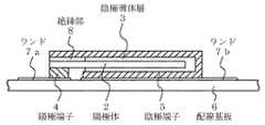
図3に、従来の表面実装型の固体電解コンデンサの一例の断面図を示す。図3を参照して、この図に示すコンデンサ1は、板状の陽極体2と、その陽極体の大部分を覆う陰極導体層3と、陽極体2の上記陰極導体層3に覆われていない部分に固着された陽極端子4と、上記陰極導体層3に固着された陰極端子5と、外装樹脂9とからなっている。
【0005】
陽極体2は、例えばアルミニウムやタンタル或いはニオブのような酸化皮膜形成性の弁作用金属の板(又は、箔。以後、特に断らない限り、「板」は「箔」も含むこととする)を母材とする。この母材金属板の表面は例えばエッチングなどによって拡面化され、その拡面化した表面に、例えば陽極酸化などによって、図示しない母材金属の酸化金属皮膜が形成されている。この酸化金属皮膜が、コンデンサの誘電体である。
【0006】
陰極導体層3は、例えば、上記陽極体の表面の酸化金属皮膜上に順次形成された固体電解質層、グラファイト層および銀ペースト層(いずれも図示せず)からなる。固体電解質層には、例えばポリピロールやポリチオフェン或いはポリアニリンなどのような導電性高分子や、二酸化マンガンのような半導体材料が用いられる。
【0007】
陽極端子4は、上述の陽極体2に、例えばレーザ溶接や抵抗溶接のような方法で導電的に固着接続されている。一方、陰極端子5は、上記陰極導体層3の最上層である銀ペースト層に接着されている。これら陽極端子4と陰極端子5とが、外部との電気的接続のための端子である。
【0008】
外装樹脂9は、例えばエポキシ樹脂のような熱硬化性樹脂を材料に用いたトランスファモールド成形により形成され、上述の陽極体2、陰極導体層3、陽極体2と陽極端子4との接続部及び陰極導体層3と陰極端子5との接続部を覆っている。この外装樹脂9は外部からの酸素や水分の侵入を防ぎ、信頼性を確保している。
【0009】
そして、陽極端子4及び陰極端子5は、外装樹脂9から引き出された部分が、外装樹脂9の側面に沿って折り曲げられ、更にその先で、外装樹脂9の底面(すなわち、このコンデンサの実装面)に沿って内向きに折り曲げられて、同一面上で向かい合っている。この陽、陰両端子4,5の上記実装面上で向かい合っている部分が、外部との接続部分である。目的の電子回路を実現するためにこのコンデンサを実装用の配線基板6に実装するときは、上記陽、陰両端子の外部との接続部分が、配線基板上に形成されている配線パターンのランド7a,7bにはんだ付けされる。
【0010】
【発明が解決しようとする課題】
上述したように、この種の従来のコンデンサにおいては、モールド樹脂で外装することにより、外部からの酸素や水分の侵入を防ぎ、信頼性を確保している。
【0011】
しかしながら、樹脂によるトランスファモールドを行う場合、溶融した樹脂が金型中を流れて行くようにするためには、金型の内壁と金型中のコンデンサ素子との間に或る程度以上の隙間を確保しなければならない。従って、外装樹脂9の厚さは必ず或る一定以上の厚さになる。コンデンサ素子と金型との間に溶融樹脂の流れに必要な厚さがない場合は、樹脂が充填されない隙間ができ、完成したコンデンサに外装樹脂9で覆われない欠陥部分ができるなどの事故が生じやすい。そして、そのような外装樹脂9の欠陥部分では、外部からの酸素や水分などの侵入を防ぐことができないので、コンデンサとしての信頼性が低下してしまうことになる。結局、コンデンサの厚さをある程度より小さくすることはできない。
【0012】
さらに、図3に示す構造においては、陽極端子4と陰極端子5をいったん外装樹脂9から引き出し、その引き出した先端を外部との接続部分にしている。従って、その長さの分、陽極端子、陰極端子の抵抗が大きくなり、コンデンサのESRが大きくなってしまう。
【0013】
従って、本発明の目的は、これまでのモールド樹脂外装のコンデンサに比べ、外部からの酸素や水分の侵入による信頼性の低下をきたすことなく、より厚さの薄い電解コンデンサを提供することにある。
【0014】
本発明は、また、これまでよりESRの小さい電解コンデンサを提供することを目的とする。
【0015】
【課題を解決するための手段】
本発明の固体電解コンデンサは、板状又は箔状の陽極体の一主面側に外部との電気的接続のための陽極端子と陰極端子とを面一になるように設けた構造の固体電解コンデンサであって、前記陽極体の前記一主面側の前記陽極端子が固着される部分を除いて当該陽極体を覆う陰極導体層を有し、その陰極導体層の前記一主面側には前記陰極端子の用をなす第1の金属板又は金属箔を密着固設して前記陰極導体層の一主面側を塞ぎ、前記陰極導体層の他の主面側には第2の金属板又は金属箔を密着固設して前記陰極導体層の他の主面側を塞ぎ、前記第1の金属板又は金属箔と前記第2の金属板又は金属箔とは、当該固体電解コンデンサの上下二面のみ、又は前記陽極体の外形に沿って断面コの字型に折れ曲がった一枚の金属板又は金属箔からなり、前記固体電解コンデンサの上下二面と前記陽極体の前記陽極端子が固着される部分の側とは反対の側の側面の三面のみに設けられ、前記陽極体と外部との間の通気を、外装樹脂を設けることなしに前記第1の金属板又は金属箔及び前記第2の金属板又は金属箔で遮断する構造にし、前記陽極体の前記陽極端子が固着される部分に前記陽極端子を導電的に固着したことを特徴とする。
【0016】
上述のコンデンサは、板状又は箔状の陽極体の一主面側に外部との電気的接続のための陽極端子と陰極端子とを面一になるように設けた構造の表面実装型の固体電解コンデンサを製造する方法であって、板状又は箔状の弁作用金属を拡面化し、表面に母材弁作用金属の酸化物の層を形成して陽極体を得る過程と、前記陽極体の一主面の前記陽極端子が固着されるべき部分を残して陽極体を覆う陰極導体層であって、前記酸化物の層を覆う固体電解質の層を少なくとも含み、最上層には導電性接着剤の層を有する陰極導体層を形成する過程と、前記陽極体の前記陰極導体層に覆われていない部分に前記陽極端子を導電的に固着する過程と、前記陰極導体層の一主面側にその主面側の陰極導体層より面積の大なる金属板又は金属箔であって、前記陰極端子の用をなすべき第1の金属板又は金属箔を前記陽極端子と面一になるように接着する過程と、陰極導体層の他の主面側にその主面側の陰極導体層より面積の大なる第2の金属板又は金属箔を接着する過程とを含み、前記第1の金属板又は金属箔と前記第2の金属板又は金属箔とは、当該固体電解コンデンサの上下二面のみ、又は前記陽極体の外形に沿って断面コの字型に折れ曲がった一枚の金属板又は金属箔からなり、前記固体電解コンデンサの上下二面と前記陽極体の前記陽極端子が固着される部分の側とは反対の側の側面の三面のみに設けられ、前記陽極体と外部との間の通気を、外装樹脂を設けることなしに前記第1の金属板又は金属箔及び前記第2の金属板又は金属箔で遮断する構造を形成するようにした固体電解コンデンサの製造方法によって製造される。
【0017】
【発明の実施の形態】
次に、本発明の実施の形態について、図面を参照して説明する。本発明の一実施例に係る表面実装型固体電解コンデンサの断面を示す図1を参照して、本発明に係る固体電解コンデンサは、陰極導体層3の上下2つの主面を、モールド樹脂に替えて金属板(陰極端子5a,5b)で塞いだ構造になっている。
【0018】
本実施例に係る固体電解コンデンサは、以下のようにして製造する。先ず、アルミニウム箔の表面をエッチングして粗化し、拡面化する。そして、陽極酸化によって母材金属のアルミニウムを酸化し、箔の表面に酸化アルミニウム(Al2 O3 )の薄膜(図示せず)を形成して陽極体2を得る。陽極体の母材弁作用金属には、エッチドアルミニウム箔に代えて、タンタルの粉末を薄板状にプレス成形し、焼結して多孔質にした板状のものを用いてもよい。勿論、ニオブのような他の弁作用金属を用いてもよい。いずれの材料や方法でも、従来公知のものが適用できる。
【0019】
そして、上記酸化アルミニウム膜上に、陽極体2の大部分を覆うようにして、固体電解質の層、グラファイト層、導電性接着剤の層(いずれも図示せず)を順次積層して、陰極導体層3を形成する。固体電解質には導電性高分子や、二酸化マンガン或いはTCNQのような半導体が利用できるが、周知のとおり、導電性高分子は他の固体電解質に比べ電気伝導度が大きいので、本発明のようにコンデンサの低ESR化を目的の一つとするときは、固体電解質には導電性高分子を用いるのが適当であろう。導電性高分子を用いるのであれば、例えばピロールやチオフェン或いはアニリンなどのモノマーを、化学酸化重合や電解酸化重合などの方法で重合させることによって形成できる。グラファイト層は、グラファイトと樹脂バインダとからなるグラファイトペーストを塗布して形成する。導電性接着剤層は、銀や銅などの金属粉末と樹脂バインダとからなる導電性ペーストを塗布して形成する。
【0020】
次に、陽極体2の一方の主面(図1の場合は、上側の面)の、陰極導体層3が形成されていない部分に絶縁性の樹脂を塗布して、絶縁部8を形成する。更に、陽極体2のもう一方の主面(同、下側の面)の陰極導体層3が形成されていない部分、つまり絶縁部8とは陽極体2を挟んで対向する部分に陽極端子4を接合する。この陽極端子4には、はんだ付けによる接合に有利で導電性のよい銅や黄銅あるいはリン青銅などの材料を用い、陽極体2との接合には、レーザ溶接、超音波溶接などの方法を利用する。一方、下側の面の陰極導体層3には、金属板(陰極端子5a)を接着する。また、上側の面の陰極導体層には、別のもう1枚の金属板(陰極端子5b)を接着する。これら陰極端子5a,5bはそれぞれ、陰極導体層3の上面側、下面側を塞ぐように、それぞれの面上の陰極導体層より若干大きい形状にし、陰極導体層3の最上層の導電性接着剤によって接着する。上面側の陰極端子5aについては、更に絶縁部8をも覆う形状にしておく。陰極端子5a,5bの材料には銅、42合金、洋白などを用いることができる。尚、絶縁部8の形成、陽極端子4の接合、陰極端子5aの接着、陰極端子5bの接着の順序は、陰極端子5aの接着が絶縁部8の後になればよく、他の作業は必ずしも上述の順でなくてもかまわない。
【0021】
本発明に係るコンデンサは、陰極導体層3の主たる面を上下2枚の陰極端子5a,5bで塞いでいる構造になっている。これらの金属板5a,5bが陰極導体層3の一番面積の大きい部分を通しての酸素や水分の侵入を防いでいるので、信頼性は確保される。陰極導体層を金属板で挟んで塞ぐことで、従来必要であったモールド樹脂による厚い被覆は不要となるので、より薄形のコンデンサを得ることができる。
【0022】
しかも、陽極体2から陽極端子や陰極端子の外部との接続部分までの距離は最短で済み、且つ両端子4,5と陽極体2との接合面積を大きく確保できるので、端子の接続に伴う内部抵抗の増加が小さく抑えられる。
【0023】
本実施例の固体電解コンデンサは、図2に示すように変形することもできる。すなわち、変形例の断面を示す図2を参照して、本変形例においては、上側の陰極端子5aと下側の陰極端子5bとを別々の2枚の金属板とせず、1枚の金属板5で構成し、陽極端子4とは反対側で陽極体2に沿って「コ」の字型に折り曲げて、陽極体2を包み込むようにする。このようにすると、実施例の効果に加えて、陽極体2の側端からの酸素、水分の侵入も遮断できるので、信頼性がより向上する。しかも、一枚の金属板を折り曲げるだけであるので、製造工程もそれほど複雑にはならないで済む。
【0024】
尚、陰極端子5a,5b(実施例1)又は陰極端子5(変形例)は、必ずしも剛性のある板でなくてもよい。通気遮断性を備えていれば、箔であってもかまわない。
【0025】
【発明の効果】
以上説明したように、本発明によれば、これまでのモールド樹脂外装型のコンデンサに比べ、外部からの酸素や水分の侵入による信頼性の低下をきたすことなく、より厚さが薄く、しかもESRの小さい表面実装型電解コンデンサを提供することができる。
【図面の簡単な説明】
【図1】本発明の一実施例に係る固体電解コンデンサの断面図である。
【図2】変形例に係る固体電解コンデンサの断面図である。
【図3】従来の表面実装型固体電解コンデンサの一例の断面図である。
【符号の説明】
2 陽極体
3 陰極導体層
4 陽極端子
5,5a,5b 陰極端子
6 配線基板
7a,7b ランド[0001]
BACKGROUND OF THE INVENTION
The present invention relates to a solid electrolytic capacitor and a method for manufacturing the same, and more particularly, to a technique effective for reducing the thickness and reducing the ESR (Equivalent Series Resistance) of a surface mount solid electrolytic capacitor.
[0002]
[Prior art]
2. Description of the Related Art In recent years, electronic devices have become smaller and lighter and portable devices have become more and more necessary, and the necessity for downsizing and thinning of electronic components has been increasing. In particular, in a portable device, since the device is not only small but must be thin at the same time, there are severe restrictions on the thickness direction of electronic components used for this, and there is a strong demand for thinning.
[0003]
Under such circumstances, not only semiconductor components but also passive components, in particular, electrolytic capacitors used for decoupling and the like in power supply circuits must be reduced in size and thickness. Conventionally, in this type of capacitor, a small capacitor element is molded as disclosed in, for example, JP-A-62-2005630, JP-A-58-157125, or JP-A-4-123416. It is widely practiced to make a small surface-mount type capacitor, so-called chip-type capacitor, by packaging with resin. In order to reduce the thickness of the capacitor element, a plate or foil is often used. A structural feature of conventional capacitors is that they are all packaged with a mold resin.
[0004]
FIG. 3 shows a cross-sectional view of an example of a conventional surface mount type solid electrolytic capacitor. Referring to FIG. 3, the capacitor 1 shown in this figure is covered with a plate-like anode body 2, a cathode conductor layer 3 that covers most of the anode body, and the cathode conductor layer 3 of the anode body 2. It comprises an anode terminal 4 fixed to a non-existing portion, a
[0005]
The anode body 2 is a valve metal plate (or foil, such as aluminum, tantalum, or niobium) (or “foil” unless otherwise specified). Use as a base material. The surface of the base metal plate is enlarged by, for example, etching, and a metal oxide film of a base metal (not shown) is formed on the enlarged surface by, for example, anodic oxidation. This metal oxide film is a capacitor dielectric.
[0006]
The cathode conductor layer 3 is composed of, for example, a solid electrolyte layer, a graphite layer, and a silver paste layer (all not shown) sequentially formed on the metal oxide film on the surface of the anode body. For the solid electrolyte layer, for example, a conductive polymer such as polypyrrole, polythiophene, or polyaniline, or a semiconductor material such as manganese dioxide is used.
[0007]
The anode terminal 4 is conductively fixedly connected to the above-described anode body 2 by a method such as laser welding or resistance welding. On the other hand, the
[0008]
The exterior resin 9 is formed by transfer molding using, for example, a thermosetting resin such as an epoxy resin, and the anode body 2, the cathode conductor layer 3, the connection portion between the anode body 2 and the anode terminal 4, and A connection portion between the cathode conductor layer 3 and the
[0009]
The portions of the anode terminal 4 and the
[0010]
[Problems to be solved by the invention]
As described above, in this type of conventional capacitor, the exterior is covered with a mold resin to prevent intrusion of oxygen and moisture from the outside and ensure reliability.
[0011]
However, when performing transfer molding with a resin, in order to allow the molten resin to flow through the mold, there is a certain gap between the inner wall of the mold and the capacitor element in the mold. Must be secured. Therefore, the thickness of the exterior resin 9 is always greater than a certain thickness. When the thickness required for the flow of the molten resin is not between the capacitor element and the mold, there is a gap that is not filled with the resin, and there is an accident such as a defective portion that is not covered with the exterior resin 9 in the completed capacitor. Prone to occur. Then, since such a defective portion of the exterior resin 9 cannot prevent the entry of oxygen, moisture, and the like from the outside, reliability as a capacitor is lowered. After all, the thickness of the capacitor cannot be made smaller than a certain level.
[0012]
Further, in the structure shown in FIG. 3, the anode terminal 4 and the
[0013]
Accordingly, it is an object of the present invention to provide an electrolytic capacitor having a thinner thickness without deteriorating reliability due to intrusion of oxygen and moisture from the outside as compared with conventional capacitors with a molded resin sheath. .
[0014]
Another object of the present invention is to provide an electrolytic capacitor having a smaller ESR than ever.
[0015]
[Means for Solving the Problems]
The solid electrolytic capacitor of the present invention is a solid electrolytic structure having a structure in which an anode terminal and a cathode terminal for electrical connection with the outside are provided on one main surface side of a plate-like or foil-like anode body. A capacitor having a cathode conductor layer covering the anode body excluding a portion to which the anode terminal on the one principal surface side of the anode body is fixed, and on the one principal surface side of the cathode conductor layer A first metal plate or metal foil serving as the cathode terminal is closely attached and closed to close one main surface side of the cathode conductor layer, and a second metal plate is formed on the other main surface side of the cathode conductor layer. or busytechnique other main surface of the cathode conductor layer of the metal foil adhesion solid and set,wherein the first metal plate or metal foil and the second metal plate or metal foil, of the solid electrolytic capacitor Consists of a single metal plate or metal foil that is folded into a U-shaped cross section along only the upper and lower surfaces or along the outer shape of the anode body. The solid to the side of the portion where the anode terminal is fixed in the upper and lower surface and the anode of the electrolytic capacitor is provided only on the three sides of the side surface of the opposite side of the vent between the anode body and theoutside, the outer A structure in which the first metal plate or the metal foil and the second metal plate or the metal foil are cut offwithout providing a resin, and the anode terminal is electrically connected to a portion of the anode body to which the anode terminal is fixed. It is characterized by adhering to.
[0016]
The above-described capacitor is a surface-mount type solid having a structure in which an anode terminal and a cathode terminal for electrical connection with the outside are provided on one main surface side of a plate-like or foil-like anode body so as to be flush with each other. A method for producing an electrolytic capacitor, comprising a step of enlarging a plate-like or foil-like valve action metal, forming an oxide layer of a base metal valve action metal on the surface, and obtaining the anode body, A cathode conductor layer covering the anode body, leaving a portion to which the anode terminal of one main surface is to be fixed, and comprising at least a solid electrolyte layer covering the oxide layer, the uppermost layer being a conductive adhesive a step of forming a cathode conductor layer having a layer of material,the steps of securing said anode terminal conductively to the not covered by the cathode conductor layer portion of the anode body, one principal surface of the cathode conductor layer A metal plate or metal foil having a larger area than the cathode conductor layer on the main surface side,A step of bonding the first metal plate or metal foil to form a use of electrode terminalsuch that the anode terminals and the flush from the cathode conductor layer of the main surface side to the other main surface of the cathode conductor layerlook includinga step of bonding the large become second metal plate or metal foilarea, wherein the first metal plate or metal foil and the second metal plate or metal foil, the top and bottom of the solid electrolytic capacitor two It consists of only one surface or a single metal plate or metal foil bent into a U-shaped cross section along the outer shape of the anode body, and the upper and lower surfaces of the solid electrolytic capacitor and the anode terminal of the anode body are fixed. The first metal plate or the metal foil and the second metal are provided on only three sides of the side opposite to the side where the first metal plate or metal foil is provided without providing exterior resin. the solid electrolytic capacitorwhich is adapted to form a metal plate or a structure for blocking a metal foil Produced by the process of production.
[0017]
DETAILED DESCRIPTION OF THE INVENTION
Next, embodiments of the present invention will be described with reference to the drawings. Referring to FIG. 1 showing a cross section of a surface-mount type solid electrolytic capacitor according to an embodiment of the present invention, the solid electrolytic capacitor according to the present invention replaces the upper and lower two main surfaces of the cathode conductor layer 3 with mold resin. The metal plate (cathode terminals 5a and 5b) is closed.
[0018]
The solid electrolytic capacitor according to this example is manufactured as follows. First, the surface of the aluminum foil is etched and roughened to enlarge the surface. Then, the base metal aluminum is oxidized by anodic oxidation, and a thin film (not shown) of aluminum oxide (Al2 O3 ) is formed on the surface of the foil to obtain the anode body 2. As the base metal valve action metal of the anode body, instead of the etched aluminum foil, a tantalum powder press-molded into a thin plate and sintered to be porous may be used. Of course, other valve metals such as niobium may be used. Any known material and method can be used.
[0019]
Then, a solid electrolyte layer, a graphite layer, and a conductive adhesive layer (all not shown) are sequentially laminated on the aluminum oxide film so as to cover most of the anode body 2, and the cathode conductor Layer 3 is formed. As the solid electrolyte, a conductive polymer or a semiconductor such as manganese dioxide or TCNQ can be used. However, as is well known, a conductive polymer has a higher electrical conductivity than other solid electrolytes. When one of the objectives is to reduce the ESR of the capacitor, it is appropriate to use a conductive polymer for the solid electrolyte. If a conductive polymer is used, it can be formed by polymerizing monomers such as pyrrole, thiophene or aniline by a method such as chemical oxidation polymerization or electrolytic oxidation polymerization. The graphite layer is formed by applying a graphite paste made of graphite and a resin binder. The conductive adhesive layer is formed by applying a conductive paste made of a metal powder such as silver or copper and a resin binder.
[0020]
Next, an insulating resin is applied to a portion of one main surface of the anode body 2 (upper surface in the case of FIG. 1) where the cathode conductor layer 3 is not formed, thereby forming the insulating
[0021]
The capacitor according to the present invention has a structure in which the main surface of the cathode conductor layer 3 is closed by two upper and lower cathode terminals 5a and 5b. Since these metal plates 5a and 5b prevent intrusion of oxygen and moisture through the largest area of the cathode conductor layer 3, reliability is ensured. By covering the cathode conductor layer with a metal plate, it is not necessary to provide a thick coating with a mold resin, which has been necessary in the past, so that a thinner capacitor can be obtained.
[0022]
In addition, the distance from the anode body 2 to the connection portion between the anode terminal and the cathode terminal and the outside of the anode body 2 can be minimized, and a large joint area can be secured between the
[0023]
The solid electrolytic capacitor of this embodiment can be modified as shown in FIG. That is, with reference to FIG. 2 which shows the cross section of a modification, in this modification, the upper cathode terminal 5a and the lower cathode terminal 5b are not two separate metal plates, but one metal plate. 5, the anode body 2 is wrapped around the anode body 2 on the side opposite to the anode terminal 4 so as to be folded in a “U” shape. In this case, in addition to the effects of the embodiment, the intrusion of oxygen and moisture from the side end of the anode body 2 can be blocked, so that the reliability is further improved. Moreover, since only one metal plate is bent, the manufacturing process is not so complicated.
[0024]
The cathode terminals 5a and 5b (Example 1) or the cathode terminal 5 (modified example) do not necessarily have to be a rigid plate. A foil may be used as long as it has a ventilation barrier.
[0025]
【The invention's effect】
As described above, according to the present invention, the thickness is thinner and the ESR is reduced without deteriorating the reliability due to the invasion of oxygen and moisture from the outside as compared with the conventional molded resin package type capacitor. Can be provided.
[Brief description of the drawings]
FIG. 1 is a cross-sectional view of a solid electrolytic capacitor according to an embodiment of the present invention.
FIG. 2 is a cross-sectional view of a solid electrolytic capacitor according to a modification.
FIG. 3 is a cross-sectional view of an example of a conventional surface mount type solid electrolytic capacitor.
[Explanation of symbols]
2 Anode body 3 Cathode conductor layer 4
Claims (7)
Translated fromJapanese前記陽極体の前記一主面側の前記陽極端子が固着される部分を除いて当該陽極体を覆う陰極導体層を有し、
その陰極導体層の前記一主面側には前記陰極端子の用をなす第1の金属板又は金属箔を密着固設して前記陰極導体層の一主面側を塞ぎ、
前記陰極導体層の他の主面側には第2の金属板又は金属箔を密着固設して前記陰極導体層の他の主面側を塞ぎ、
前記第1の金属板又は金属箔と前記第2の金属板又は金属箔とは、前記固体電解コンデンサの上下二面のみ、又は前記陽極体の外形に沿って断面コの字型に折れ曲がった1枚の金属板又は金属箔からなり、前記固体電解コンデンサの上下二面と前記陽極体の前記陽極端子が固着される部分の側とは反対の側の側面の三面のみに設けられ、
前記陽極体と外部との間の通気を、外装樹脂を設けることなしに前記第1の金属板又は金属箔及び前記第2の金属板又は金属箔で遮断する構造にし、
前記陽極体の前記陽極端子が固着される部分に前記陽極端子を導電的に固着したことを特徴とする固体電解コンデンサ。A solid electrolytic capacitor having a structure in which an anode terminal and a cathode terminal for electrical connection with the outside are provided on one main surface side of a plate-like or foil-like anode body,
A cathode conductor layer that covers the anode body except a portion to which the anode terminal on the one main surface side of the anode body is fixed;
A first metal plate or metal foil serving as the cathode terminal is tightly fixed to the one principal surface side of the cathode conductor layer to close one principal surface side of the cathode conductor layer;
Another is on the main surface side busytechnique other main surface of the cathode conductor layer is fixedly provided in close contact with the second metal plate or metal foil of the cathode conductor layer,
The first metal plate or metal foil and the second metal plate or metal foil are bent into a U-shaped cross section only along two upper and lower surfaces of the solid electrolytic capacitor or along the outer shape of the anode body. Consisting of a sheet of metal plate or metal foil, provided on only the three surfaces of the upper and lower surfaces of the solid electrolytic capacitor and the side of the anode body opposite to the portion to which the anode terminal is fixed,
The ventilation between the anode body and the outside is configured to be blocked by the first metal plate or metal foil and the second metal plate or metal foilwithout providing an exterior resin ,
A solid electrolytic capacitor, wherein the anode terminal is conductively fixed to a portion of the anode body to which the anode terminal is fixed.
板状又は箔状の弁作用金属を母材とし表面にはその母材弁作用金属の酸化物の層からなる誘電体層が形成された陽極体と、
前記陽極体を一主面の所定の部分を残して覆う陰極導体層であって、前記誘電体層上に形成された固体電解質層を少なくとも含み、最上層には導電性接着剤の層を有する陰極導体層と、
前記陽極体の一主面上の前記陰極導体層から露出する部分に導電的に固着された、外部との電気的接続のための陽極端子と、
前記陰極導体層の前記一主面側の導電性接着剤に接着されて、前記陽極端子と面一となるよう設けられ、前記陰極導体層の一主面側を塞ぐと共に外部との電気的接続のための陰極端子の用をなす第1の金属板又は金属箔と、
前記陰極導体層の他の主面側の導電性接着剤に接着されて、前記陰極導体層の他の主面側を塞ぐ第2の金属板又は金属箔とを備え、
前記第1の金属板又は金属箔と前記第2の金属板又は金属箔とは、当該固体電解コンデンサの上下二面のみ、又は前記陽極体の外形に沿って断面コの字型に折れ曲がった1枚の金属板又は金属箔からなり、前記固体電解コンデンサの上下二面と前記陽極体の前記陽極端子が固着される部分の側とは反対の側の側面の三面のみに設けられ、
前記陽極体と外部との間の通気を、外装樹脂を設けることなしに前記第1の金属板又は金属箔及び前記第2の金属板又は金属箔で遮断する構造の表面実装型の固体電解コンデンサ。In solid electrolytic capacitors,
An anode body having a plate-like or foil-like valve action metal as a base material and a surface formed with a dielectric layer made of an oxide layer of the base material valve action metal;
A cathode conductor layer that covers the anode body except for a predetermined portion of one main surface, and includes at least a solid electrolyte layer formed on the dielectric layer, and the uppermost layer has a conductive adhesive layer A cathode conductor layer;
An anode terminal for electrical connection with the outside, conductively fixed to a portion exposed from the cathode conductor layer on one main surface of the anode body;
Adhered to the conductive adhesive on the one principal surface side of the cathode conductor layer,and provided to be flush with the anode terminal , closes the one principal surface side of the cathode conductor layer and electrically connects to the outside A first metal plate or metal foil serving as a cathode terminal for
A second metal plate or a metal foil that is adhered to the conductive adhesive on the other main surface side of the cathode conductor layer and closes the other main surface side of the cathode conductor layer;
The first metal plate or metal foil and the second metal plate or metal foil are bent into a U-shaped cross section only along the upper and lower surfaces of the solid electrolytic capacitor or along the outer shape of the anode body. Consisting of a sheet of metal plate or metal foil, provided on only the three surfaces of the upper and lower surfaces of the solid electrolytic capacitor and the side of the anode body opposite to the portion to which the anode terminal is fixed,
Venting said first metal plate or metal foil and the second metal plate or surface mount type solid electrolytic capacitor having a structure for blocking a metal foilwithout providing the outer coating between the anode body and the outside .
板状又は箔状の弁作用金属を拡面化し、表面に母材弁作用金属の酸化物の層を形成して陽極体を得る過程と、
前記陽極体の一主面の前記陽極端子が固着されるべき部分を残して陽極体を覆う陰極導体層であって、前記酸化物の層を覆う固体電解質の層を少なくとも含み、最上層には導電性接着剤の層を有する陰極導体層を形成する過程と、
前記陽極体の前記陰極導体層に覆われていない部分に前記陽極端子を導電的に固着する過程と、
前記陰極導体層の一主面側にその主面側の陰極導体層より面積の大なる金属板又は金属箔であって、前記陰極端子の用をなすべき第1の金属板又は金属箔を前記陽極端子と面一になるように接着する過程と、
陰極導体層の他の主面側にその主面側の陰極導体層より面積の大なる第2の金属板又は金属箔を接着する過程とを含み、
前記第1の金属板又は金属箔と前記第2の金属板又は金属箔とは、当該固体電解コンデンサの上下二面のみ、又は前記陽極体の外形に沿って断面コの字型に折れ曲がった一枚の金属板又は金属箔からなり、前記固体電解コンデンサの上下二面と前記陽極体の前記陽極端子が固着される部分の側とは反対の側の側面の三面のみに設けられ、前記陽極体と外部との間の通気を、外装樹脂を設けることなしに前記第1の金属板又は金属箔及び前記第2の金属板又は金属箔で遮断する構造を形成するようにした固体電解コンデンサの製造方法。A surface mount type solid electrolytic capacitor having a structure in which an anode terminal and a cathode terminal for electrical connection with the outside are provided on one main surface side of a plate-like or foil-like anode body so as to be flush with each other is manufactured. A method,
Process of expanding the plate-like or foil-like valve action metal, forming an oxide layer of the base metal valve action metal on the surface, and obtaining an anode body,
A cathode conductor layer covering the anode body except for a portion to which the anode terminal of one main surface of the anode body is to be fixed, and including at least a solid electrolyte layer covering the oxide layer, Forming a cathode conductor layer having a layer of conductive adhesive;
Aprocess of electrically fixing the anode terminal to a portion of the anode body not covered with the cathode conductor layer;
A large becomes a metal plate or a metal foil area from a cathode conductor layer on the main surface on one main side of the cathode conductor layer,wherein the first metal plate or metal foil to form a use of the cathode terminala step of bondingso that the anode terminal flush,
Look includinga step of bonding the large become second metal plate or metal foil area from a cathode conductor layer on the main surface side to the other main surface of the cathode conductorlayer,
The first metal plate or metal foil and the second metal plate or metal foil are bent in a U-shaped cross section along only the upper and lower surfaces of the solid electrolytic capacitor or along the outer shape of the anode body. The anode body is composed of a sheet of metal plate or metal foil, and is provided only on three surfaces of the upper and lower surfaces of the solid electrolytic capacitor and the side surface of the anode body opposite to the portion to which the anode terminal is fixed. Of a solid electrolytic capacitorin which a structure is formed in which ventilation between the outside and the outside is blocked by the first metal plate or metal foil and the second metal plate or metal foil without providing an exterior resin. Method.
Priority Applications (5)
| Application Number | Priority Date | Filing Date | Title |
|---|---|---|---|
| JP2002046248AJP4142878B2 (en) | 2002-02-22 | 2002-02-22 | Solid electrolytic capacitor and manufacturing method thereof |
| US10/369,473US6765784B2 (en) | 2002-02-22 | 2003-02-20 | Solid electrolytic capacitor and manufacturing method for the same |
| TW092103602ATWI277989B (en) | 2002-02-22 | 2003-02-21 | Solid electrolytic capacitor and manufacturing method for the same |
| KR1020030010942AKR100623804B1 (en) | 2002-02-22 | 2003-02-21 | SOLID ELECTROLYTE CAPACITOR AND METHOD FOR MANUFACTURING THE SAME |
| CNB031227007ACN100477034C (en) | 2002-02-22 | 2003-02-22 | Solid electrolytic capacitor and manufacturing method thereof |
Applications Claiming Priority (1)
| Application Number | Priority Date | Filing Date | Title |
|---|---|---|---|
| JP2002046248AJP4142878B2 (en) | 2002-02-22 | 2002-02-22 | Solid electrolytic capacitor and manufacturing method thereof |
Publications (2)
| Publication Number | Publication Date |
|---|---|
| JP2003249418A JP2003249418A (en) | 2003-09-05 |
| JP4142878B2true JP4142878B2 (en) | 2008-09-03 |
Family
ID=27784486
Family Applications (1)
| Application Number | Title | Priority Date | Filing Date |
|---|---|---|---|
| JP2002046248AExpired - LifetimeJP4142878B2 (en) | 2002-02-22 | 2002-02-22 | Solid electrolytic capacitor and manufacturing method thereof |
Country Status (5)
| Country | Link |
|---|---|
| US (1) | US6765784B2 (en) |
| JP (1) | JP4142878B2 (en) |
| KR (1) | KR100623804B1 (en) |
| CN (1) | CN100477034C (en) |
| TW (1) | TWI277989B (en) |
Families Citing this family (16)
| Publication number | Priority date | Publication date | Assignee | Title |
|---|---|---|---|---|
| JP4354227B2 (en)* | 2003-07-23 | 2009-10-28 | Tdk株式会社 | Solid electrolytic capacitor |
| US7016180B2 (en)* | 2003-12-26 | 2006-03-21 | Tdk Corporation | Capacitor |
| US6870728B1 (en)* | 2004-01-29 | 2005-03-22 | Tdk Corporation | Electrolytic capacitor |
| KR100610462B1 (en) | 2004-02-20 | 2006-08-08 | 엔이씨 도낀 가부시끼가이샤 | Solid electrolytic capacitor, transmission-line device, method of producing the same, and composite electronic component using the same |
| US7715174B1 (en)* | 2004-05-17 | 2010-05-11 | Pacesetter, Inc. | Electrolytic capacitors with alternate cathode materials for use in pulse discharge applications |
| TWI270905B (en)* | 2004-07-14 | 2007-01-11 | Sanyo Electric Co | Solid electrolytic condenser and manufacturing method of the same |
| US7385802B1 (en)* | 2005-10-05 | 2008-06-10 | Pacesetter Inc. | Electrolytic capacitor |
| US8414962B2 (en) | 2005-10-28 | 2013-04-09 | The Penn State Research Foundation | Microcontact printed thin film capacitors |
| ITMI20060056A1 (en)* | 2006-01-16 | 2007-07-17 | Getters Spa | ELECTROLYTIC CONDENSER INCLUDING MEANS FOR THE ABSORPTION OF HARMFUL SUBSTANCES |
| US7495890B2 (en)* | 2006-08-04 | 2009-02-24 | Kemet Electronics Corporation | Method of improving cathode connection integrity in solid electrolytic capacitors using secondary adhesive |
| US7280343B1 (en) | 2006-10-31 | 2007-10-09 | Avx Corporation | Low profile electrolytic capacitor assembly |
| US7745281B2 (en)* | 2007-03-07 | 2010-06-29 | Kemet Electronics Corporation | Thin solid electrolytic capacitor embeddable in a substrate |
| KR100914890B1 (en)* | 2007-12-17 | 2009-08-31 | 삼성전기주식회사 | Solid electrolytic condenser and method for manufacturing the same |
| US8062385B2 (en)* | 2008-02-12 | 2011-11-22 | Kemet Electronics Corporation | Solid electrolytic capacitor with improved volumetric efficiency method of making |
| US8125766B2 (en)* | 2008-06-13 | 2012-02-28 | Kemet Electronics Corporation | Concentrated capacitor assembly |
| US9941056B2 (en)* | 2013-01-25 | 2018-04-10 | Kemet Electronics Corporation | Solid electrolytic capacitor and method |
Family Cites Families (7)
| Publication number | Priority date | Publication date | Assignee | Title |
|---|---|---|---|---|
| JPS58157125A (en) | 1982-03-12 | 1983-09-19 | マルコン電子株式会社 | Method of producing chip type aluminum electrolytic condenser |
| JPS625630A (en) | 1985-07-02 | 1987-01-12 | 松下電器産業株式会社 | Aluminum electrolytic capacitor |
| JP2973499B2 (en) | 1990-09-13 | 1999-11-08 | 松下電器産業株式会社 | Chip type solid electrolytic capacitor |
| JP3568432B2 (en) | 1999-09-30 | 2004-09-22 | 三洋電機株式会社 | Method for manufacturing solid electrolytic capacitor |
| KR100359055B1 (en)* | 2000-04-25 | 2002-11-07 | 한국과학기술연구원 | Thin film super capacitor and its fabrication method |
| US6400557B1 (en)* | 2000-06-02 | 2002-06-04 | Motorola, Inc. | Capacitor with folded end plate tab configuration |
| JP3319464B2 (en) | 2001-04-26 | 2002-09-03 | 松下電器産業株式会社 | Laser trimmable condenser |
- 2002
- 2002-02-22JPJP2002046248Apatent/JP4142878B2/ennot_activeExpired - Lifetime
- 2003
- 2003-02-20USUS10/369,473patent/US6765784B2/ennot_activeExpired - Lifetime
- 2003-02-21TWTW092103602Apatent/TWI277989B/ennot_activeIP Right Cessation
- 2003-02-21KRKR1020030010942Apatent/KR100623804B1/ennot_activeExpired - Fee Related
- 2003-02-22CNCNB031227007Apatent/CN100477034C/ennot_activeExpired - Lifetime
Also Published As
| Publication number | Publication date |
|---|---|
| US6765784B2 (en) | 2004-07-20 |
| CN1444241A (en) | 2003-09-24 |
| CN100477034C (en) | 2009-04-08 |
| KR100623804B1 (en) | 2006-09-18 |
| US20030169561A1 (en) | 2003-09-11 |
| TWI277989B (en) | 2007-04-01 |
| JP2003249418A (en) | 2003-09-05 |
| TW200303564A (en) | 2003-09-01 |
| KR20030069886A (en) | 2003-08-27 |
Similar Documents
| Publication | Publication Date | Title |
|---|---|---|
| JP4142878B2 (en) | Solid electrolytic capacitor and manufacturing method thereof | |
| US6807045B2 (en) | Thin surface mounted type solid electrolytic capacitor | |
| US7542267B2 (en) | Lead frame, method of manufacturing a face-down terminal solid electrolytic capacitor using the lead frame, and face-down terminal solid electrolytic capacitor manufactured by the method | |
| JP3920670B2 (en) | Solid electrolytic capacitor | |
| JP2007287828A (en) | Solid electrolytic capacitor and manufacturing method thereof | |
| US6775125B2 (en) | Solid electrolytic capacitor and method of manufacturing the capacitor | |
| JP5020432B2 (en) | Chip type multilayer capacitor | |
| JP2002237431A (en) | Solid electrolytic capacitor and method of manufacturing the same | |
| JP4802550B2 (en) | Solid electrolytic capacitor | |
| US9659714B2 (en) | Solid electrolytic capacitor including insulating substrate having recessed surface | |
| CN111095452A (en) | Solid electrolytic capacitor and method of making the same | |
| JP4337423B2 (en) | Circuit module | |
| JP2002110461A (en) | Solid-state electrolytic chip capacitor | |
| JP4613669B2 (en) | Solid electrolytic capacitor | |
| JP2007013043A (en) | Electrode assembly for mounting electric element, electric component employing the same, and solid electrolytic capacitor | |
| JP2005311216A (en) | Solid electrolytic capacitor and manufacturing method thereof | |
| JP3958725B2 (en) | Surface mount thin capacitor and manufacturing method thereof | |
| JP2972304B2 (en) | Solid electrolytic capacitors | |
| JP2526281Y2 (en) | Solid electrolytic capacitors | |
| JP2002299159A (en) | Regulator for power supply | |
| JP2006060017A (en) | Surface-mounting thin capacitor | |
| JPH05144687A (en) | Manufacture of solid electrolytic capacitor | |
| JP2002289478A (en) | Solid electrolytic capacitor and method of manufacturing the same | |
| JP2002299162A (en) | Regulator for power supply | |
| JPH0582400A (en) | Solid electrolytic capacitor |
Legal Events
| Date | Code | Title | Description |
|---|---|---|---|
| A977 | Report on retrieval | Free format text:JAPANESE INTERMEDIATE CODE: A971007 Effective date:20050131 | |
| A131 | Notification of reasons for refusal | Free format text:JAPANESE INTERMEDIATE CODE: A131 Effective date:20050309 | |
| A521 | Request for written amendment filed | Free format text:JAPANESE INTERMEDIATE CODE: A523 Effective date:20050428 | |
| A131 | Notification of reasons for refusal | Free format text:JAPANESE INTERMEDIATE CODE: A131 Effective date:20050713 | |
| A521 | Request for written amendment filed | Free format text:JAPANESE INTERMEDIATE CODE: A523 Effective date:20050909 | |
| A02 | Decision of refusal | Free format text:JAPANESE INTERMEDIATE CODE: A02 Effective date:20051124 | |
| A521 | Request for written amendment filed | Free format text:JAPANESE INTERMEDIATE CODE: A523 Effective date:20060123 | |
| A911 | Transfer to examiner for re-examination before appeal (zenchi) | Free format text:JAPANESE INTERMEDIATE CODE: A911 Effective date:20060201 | |
| A912 | Re-examination (zenchi) completed and case transferred to appeal board | Free format text:JAPANESE INTERMEDIATE CODE: A912 Effective date:20060414 | |
| A521 | Request for written amendment filed | Free format text:JAPANESE INTERMEDIATE CODE: A523 Effective date:20080424 | |
| A01 | Written decision to grant a patent or to grant a registration (utility model) | Free format text:JAPANESE INTERMEDIATE CODE: A01 | |
| A61 | First payment of annual fees (during grant procedure) | Free format text:JAPANESE INTERMEDIATE CODE: A61 Effective date:20080613 | |
| FPAY | Renewal fee payment (event date is renewal date of database) | Free format text:PAYMENT UNTIL: 20110620 Year of fee payment:3 | |
| R150 | Certificate of patent or registration of utility model | Ref document number:4142878 Country of ref document:JP Free format text:JAPANESE INTERMEDIATE CODE: R150 Free format text:JAPANESE INTERMEDIATE CODE: R150 | |
| FPAY | Renewal fee payment (event date is renewal date of database) | Free format text:PAYMENT UNTIL: 20110620 Year of fee payment:3 | |
| FPAY | Renewal fee payment (event date is renewal date of database) | Free format text:PAYMENT UNTIL: 20120620 Year of fee payment:4 | |
| FPAY | Renewal fee payment (event date is renewal date of database) | Free format text:PAYMENT UNTIL: 20120620 Year of fee payment:4 | |
| FPAY | Renewal fee payment (event date is renewal date of database) | Free format text:PAYMENT UNTIL: 20130620 Year of fee payment:5 | |
| FPAY | Renewal fee payment (event date is renewal date of database) | Free format text:PAYMENT UNTIL: 20140620 Year of fee payment:6 | |
| S533 | Written request for registration of change of name | Free format text:JAPANESE INTERMEDIATE CODE: R313533 | |
| R350 | Written notification of registration of transfer | Free format text:JAPANESE INTERMEDIATE CODE: R350 | |
| R250 | Receipt of annual fees | Free format text:JAPANESE INTERMEDIATE CODE: R250 | |
| R250 | Receipt of annual fees | Free format text:JAPANESE INTERMEDIATE CODE: R250 | |
| EXPY | Cancellation because of completion of term |