JP4142066B2 - Electro-optical device and electronic apparatus - Google Patents
Electro-optical device and electronic apparatusDownload PDFInfo
- Publication number
- JP4142066B2 JP4142066B2JP2006153106AJP2006153106AJP4142066B2JP 4142066 B2JP4142066 B2JP 4142066B2JP 2006153106 AJP2006153106 AJP 2006153106AJP 2006153106 AJP2006153106 AJP 2006153106AJP 4142066 B2JP4142066 B2JP 4142066B2
- Authority
- JP
- Japan
- Prior art keywords
- sensor
- electrode
- bidirectional diode
- gate
- semiconductor
- Prior art date
- Legal status (The legal status is an assumption and is not a legal conclusion. Google has not performed a legal analysis and makes no representation as to the accuracy of the status listed.)
- Active
Links
Images


Classifications
- H—ELECTRICITY
- H10—SEMICONDUCTOR DEVICES; ELECTRIC SOLID-STATE DEVICES NOT OTHERWISE PROVIDED FOR
- H10D—INORGANIC ELECTRIC SEMICONDUCTOR DEVICES
- H10D86/00—Integrated devices formed in or on insulating or conducting substrates, e.g. formed in silicon-on-insulator [SOI] substrates or on stainless steel or glass substrates
- H10D86/40—Integrated devices formed in or on insulating or conducting substrates, e.g. formed in silicon-on-insulator [SOI] substrates or on stainless steel or glass substrates characterised by multiple TFTs
- H10D86/441—Interconnections, e.g. scanning lines
- H—ELECTRICITY
- H10—SEMICONDUCTOR DEVICES; ELECTRIC SOLID-STATE DEVICES NOT OTHERWISE PROVIDED FOR
- H10D—INORGANIC ELECTRIC SEMICONDUCTOR DEVICES
- H10D86/00—Integrated devices formed in or on insulating or conducting substrates, e.g. formed in silicon-on-insulator [SOI] substrates or on stainless steel or glass substrates
- H10D86/40—Integrated devices formed in or on insulating or conducting substrates, e.g. formed in silicon-on-insulator [SOI] substrates or on stainless steel or glass substrates characterised by multiple TFTs
- H10D86/481—Integrated devices formed in or on insulating or conducting substrates, e.g. formed in silicon-on-insulator [SOI] substrates or on stainless steel or glass substrates characterised by multiple TFTs integrated with passive devices, e.g. auxiliary capacitors
- H—ELECTRICITY
- H10—SEMICONDUCTOR DEVICES; ELECTRIC SOLID-STATE DEVICES NOT OTHERWISE PROVIDED FOR
- H10D—INORGANIC ELECTRIC SEMICONDUCTOR DEVICES
- H10D86/00—Integrated devices formed in or on insulating or conducting substrates, e.g. formed in silicon-on-insulator [SOI] substrates or on stainless steel or glass substrates
- H10D86/40—Integrated devices formed in or on insulating or conducting substrates, e.g. formed in silicon-on-insulator [SOI] substrates or on stainless steel or glass substrates characterised by multiple TFTs
- H10D86/60—Integrated devices formed in or on insulating or conducting substrates, e.g. formed in silicon-on-insulator [SOI] substrates or on stainless steel or glass substrates characterised by multiple TFTs wherein the TFTs are in active matrices
Landscapes
- Liquid Crystal (AREA)
- Devices For Indicating Variable Information By Combining Individual Elements (AREA)
- Solid State Image Pick-Up Elements (AREA)
- Control Of Indicators Other Than Cathode Ray Tubes (AREA)
- Thin Film Transistor (AREA)
Description
Translated fromJapanese本発明は、素子基板上で信号線が静電保護素子を介して共通配線に電気的に接続された電気光学装置、およびこの電気光学装置を備えた電子機器に関するものである。 The present invention relates to an electro-optical device in which a signal line is electrically connected to a common wiring via an electrostatic protection element on an element substrate, and an electronic apparatus including the electro-optical device.
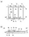
液晶装置、エレクトロルミネッセンス表示装置、撮像装置などの電気光学装置のうち、例えば、アクティブマトリクス型の液晶装置に用いられている素子基板には、図13(a)に示すように、互いに交差して延びた複数のデータ線6aおよび複数の走査線3aと、データ線6aと走査線3aとの交差部に対応して構成された複数の画素領域1eとが形成されている。 Among electro-optical devices such as liquid crystal devices, electroluminescence display devices, and imaging devices, for example, element substrates used in active matrix liquid crystal devices cross each other as shown in FIG. A plurality of
このような素子基板10では基体として絶縁基板が用いられている。このため、製造工程に素子基板10に侵入した静電気によって、画素領域1eに形成した画素トランジスタ1cが損傷しないように、素子基板10では、データ線6aおよび走査線3aを、双方向ダイオード素子Diからなる静電保護素子を介して共通配線VCOMに電気的に接続し、この共通配線VCOMを、双方向ダイオード素子Diからなる静電保護素子を介してガードリングに電気的に接続した構造が採用されている。このような双方向ダイオード素子Diは、図13(b)に示すように、一対のソース・ドレイン電極、チャネル領域を備えた半導体層、およびチャネル領域にゲート絶縁膜を介して対向するゲート電極を備えた半導体素子1sを互いに逆向きに電気的に接続するとともに、いずれの半導体素子1sにおいても、ソース・ドレイン電極のうちの一方をゲート電極に接続した構造を備えている(例えば、特許文献1参照)。
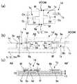
ここに本願出願人は、図14に示すように、素子基板10上にセンサ素子1hおよびセンサ用信号線1jを形成して照度や温度などの状態量を検出し、それに応じて液晶装置における表示動作を制御することを提案するものである。その場合、センサ素子1hについても静電気から保護する必要があることから、センサ用信号線1jについても、双方向ダイオード素子Diからなる静電保護素子を介して共通配線VCOMに電気的に接続することが好ましい。
Here, as shown in FIG. 14, the applicant of the present application forms a
しかしながら、センサ用信号線1jに対する静電保護素子として、図13(b)に示すような双方向ダイオード素子Diを用いると、双方向ダイオード素子Diの漏れ電流がセンサ素子1hからの信号出力に影響を及ぼし、検出精度が低下するという問題点がある。かかる問題点は、特許文献1に開示されているように、製造工程の終盤で双方向ダイオード素子Diを切り離せば解消できるものの、かかる工程を追加すると生産性が低下するとともに、双方向ダイオード素子Diの位置によって切り離しが不可能である。 However, when a bidirectional diode element Di as shown in FIG. 13B is used as an electrostatic protection element for the
以上の問題点に鑑みて、本発明の課題は、素子基板上に形成したセンサ用信号線を双方向ダイオード素子を介して共通配線に電気的に接続して静電気からの静電保護を行った場合に、双方向ダイオード素子を切り離さなくてもセンサ素子による検出を高い精度で行うことのできる電気光学装置、およびこの電気光学装置を用いた電子機器を提供することにある。 In view of the above problems, an object of the present invention is to provide electrostatic protection from static electricity by electrically connecting a sensor signal line formed on an element substrate to a common wiring via a bidirectional diode element. In this case, it is an object to provide an electro-optical device that can perform detection by a sensor element with high accuracy without separating a bidirectional diode element, and an electronic apparatus using the electro-optical device.
上記課題を解決するために、本発明では、複数のデータ線と、複数の走査線と、前記複数の走査線と前記複数の走査線とに接続された複数の画素トランジスタと、が形成されてなる素子基板を備えた電気光学装置において、前記素子基板には、センサ素子と、該センサ素子から信号出力を行うセンサ用信号線と、共通配線と、ソース電極、ドレイン電極、チャネル領域を備えた半導体層、および当該チャネル領域にゲート絶縁膜を介して対向するゲート電極を有する半導体素子と、前記ソース電極および前記ドレイン電極のうちの一方と前記ゲート電極との間に介挿された容量素子と、を備えた2つの容量結合動作型ダイオード素子を互いに逆向きに電気的に接続した容量結合動作型双方向ダイオード素子と、が形成され、前記センサ用信号線は、前記容量結合動作型双方向ダイオード素子を介して前記共通配線に電気的に接続され、前記容量結合動作型双方向ダイオード素子に対しては、前記半導体素子を非導通状態とするゲート電圧を前記ゲート電極に供給するための制御用配線が形成されていることを特徴とする。センサ素子、センサ用信号線、共通配線、半導体素子、容量結合動作型双方向ダイオード素子は、複数のデータ線と複数の走査線との交差に対応して形成された画素領域が配置されている領域の端部に形成される。
In order to solve the above problems, in the present invention, aplurality of data lines, a plurality of scanning lines, and a plurality of pixel transistors connected to the plurality of scanning lines and the plurality of scanning lines are formed. The element substrate includes a sensor element, a sensor signal line for outputting a signal from the sensor element, a common wiring, a source electrode, a drain electrode, and a channel region. A semiconductor element having a semiconductor layer and a gate electrode facing the channel region with a gate insulating film interposed therebetween; and a capacitor element interposed between one of the source electrode and the drain electrode and the gate electrode; , Two capacitively coupled operation type diode elements electrically connected in opposite directions to each other, and the sensor signal Is electrically connected to the common wiring via the capacitive coupling type bidirectional diode element, and a gate voltage for making the semiconductor element non-conductive is applied to the capacitive coupling type bidirectional diode element. Control wiring for supplying to the gate electrode is formed.In the sensor element, the sensor signal line, the common wiring, thesemiconductor element, and the capacitively coupled operation type bidirectional diode element, pixel regions formed corresponding to the intersections of the plurality of data lines and the plurality of scanning lines are arranged. It is formed at the end of the region.
本発明では、素子基板上にセンサ素子が形成されているため、このセンサ素子によって、例えば電気光学装置が置かれた環境での照度を検出し、照度に対応した条件で電気光学装置での画像表示を行うことができる。また、センサ素子から信号出力を行うセンサ用信号線は、容量結合動作型双方向ダイオード素子を介して共通配線に電気的に接続されているので、電気光学装置の製造途中などおいて素子基板に静電気が侵入した場合でも、かかる静電気を容量結合動作型双方向ダイオード素子を介して共通配線に逃がすことができ、センサ素子を静電気から保護することができる。ここで、センサ用信号線に接続する容量結合動作型双方向ダイオード素子は、ソース・ドレイン電極のうちの一方とゲート電極との間に容量素子が介挿された構造になっているので、容量結合動作型双方向ダイオード素子を構成する半導体素子に寄生容量が生じている場合でも、静電気に起因する高い電圧がセンサ用信号線と共通配線との間に発生した場合には寄生容量と容量素子との容量結合により半導体素子が導通状態になり、静電気を逃がすことができる。また、容量結合動作型双方向ダイオード素子は、一対のソース・ドレイン電極のうちの一方とゲート電極とを直結させたダイオード素子と比較して、製造工程の比較的早い時期に完成し、それ以降に発生した静電気を逃がすので、製造工程の比較的早い時期からセンサ素子を静電気から保護することができる。さらに、容量結合動作型双方向ダイオード素子を構成する半導体素子のゲート電極に対しては制御用配線が形成されているため、制御用配線からゲート電極に所定のゲート電圧を印加すれば、容量結合動作型双方向ダイオード素子を確実に非導通状態とすることができるので、容量結合動作型双方向ダイオード素子は、センサ素子から出力される信号に影響を及ぼさない。それ故、素子基板上に形成したセンサ用信号線を双方向ダイオード素子を介して共通配線に電気的に接続して静電気からの静電保護を行った場合でも、双方向ダイオード素子を切り離さなくてもセンサ素子による検出を高い精度で行うことができる。 In the present invention, since the sensor element is formed on the element substrate, the illuminance in the environment where the electro-optical device is placed is detected by the sensor element, for example, and the image in the electro-optical device is subjected to conditions corresponding to the illuminance. Display can be made. In addition, the sensor signal line for outputting a signal from the sensor element is electrically connected to the common wiring via the capacitive coupling operation type bidirectional diode element. Even when static electricity enters, such static electricity can be released to the common wiring via the capacitively coupled bidirectional diode element, and the sensor element can be protected from static electricity. Here, the capacitively coupled operation type bidirectional diode element connected to the sensor signal line has a structure in which a capacitive element is interposed between one of the source and drain electrodes and the gate electrode. Even when a parasitic capacitance is generated in the semiconductor element constituting the coupled operation type bidirectional diode element, if a high voltage caused by static electricity is generated between the sensor signal line and the common wiring, the parasitic capacitance and the capacitance element As a result of the capacitive coupling, the semiconductor element becomes conductive, and static electricity can be released. In addition, the capacitively coupled operation type bidirectional diode element is completed at a relatively early stage of the manufacturing process as compared with a diode element in which one of a pair of source / drain electrodes and a gate electrode are directly connected. Therefore, the sensor element can be protected from static electricity at a relatively early stage of the manufacturing process. Furthermore, since a control wiring is formed on the gate electrode of the semiconductor element constituting the capacitive coupling operation type bidirectional diode element, if a predetermined gate voltage is applied from the control wiring to the gate electrode, capacitive coupling is performed. Since the operation type bidirectional diode element can be surely turned off, the capacitively coupled operation type bidirectional diode element does not affect the signal output from the sensor element. Therefore, even when the sensor signal line formed on the element substrate is electrically connected to the common wiring via the bidirectional diode element to protect against static electricity, the bidirectional diode element is not separated. In addition, detection by the sensor element can be performed with high accuracy.
本発明において、前記容量結合動作型双方向ダイオード素子では、前記ソース電極および前記ドレイン電極のうちの一方と前記ゲート電極とが絶縁膜を介して対向して前記容量素子が構成されていることが好ましい。このように構成すると、容量結合動作型双方向ダイオード素子は、製造工程の比較的早い時期に完成し、製造工程の比較的早い時期からセンサ素子を静電気から保護することができる。 In the present invention, in the capacitively coupled operation type bidirectional diode element, the capacitive element is configured such that one of the source electrode and the drain electrode and the gate electrode face each other with an insulating film interposed therebetween. preferable. With this configuration, the capacitively coupled bidirectional diode element is completed at a relatively early stage in the manufacturing process, and the sensor element can be protected from static electricity at a relatively early stage in the manufacturing process.
本発明において、前記センサ素子は、ソース電極、ドレイン電極、チャネル領域を備えた半導体層、および当該チャネル領域にゲート絶縁膜を介して対向するゲート電極を備えた半導体素子と、該半導体素子に並列に電気的に接続された容量素子と、を備え、当該容量素子に対する充電を行った後、当該半導体素子を介しての放電特性に基づいて状態量が検出される構成を採用することができる。 In the present invention, the sensor element includes a semiconductor layer including a source electrode, a drain electrode, a channel region, a gate electrode facing the channel region with a gate insulating film interposed therebetween, and a parallel semiconductor element. And a capacitive element electrically connected to the capacitor element, and after charging the capacitive element, a configuration in which the state quantity is detected based on a discharge characteristic through the semiconductor element can be employed.
本発明において、前記容量結合動作型双方向ダイオード素子と前記センサ素子は、ソー
ス電極同士、ドレイン電極同士、半導体層同士、およびゲート電極同士が同一の層間に同一材料により形成されていることが好ましい。このように構成すると、共通の製造工程によって、容量結合動作型双方向ダイオード素子とセンサ素子とを形成することができる。In the present invention, in the capacitively coupled operation type bidirectional diode element and the sensor element, it is preferable that source electrodes, drain electrodes, semiconductor layers, and gate electrodes are formed of the same material between the same layers. . With this configuration, the capacitively coupled bidirectional diode element and the sensor element can be formed by a common manufacturing process.
本発明において、前記センサ素子のチャネル領域は、アモルファスシリコン膜、低温プロセスで形成した多結晶ポリシリコン、高温プロセスで形成した多結晶ポリシリコンなどを用いることができる。但し、これらの半導体膜のうち、アモルファスシリコン膜をセンサ素子のチャネル領域として用いると、照度などに対する感度の高いセンサ素子を構成することができる。 In the present invention, the channel region of the sensor element may be an amorphous silicon film, polycrystalline polysilicon formed by a low temperature process, polycrystalline polysilicon formed by a high temperature process, or the like. However, among these semiconductor films, when an amorphous silicon film is used as the channel region of the sensor element, a sensor element having high sensitivity to illuminance or the like can be configured.
本発明において、前記センサ素子は、例えば、光センサ素子を構成している。本発明において、前記センサ素子は、温度センサ素子を構成する場合もある。 In the present invention, the sensor element constitutes, for example, an optical sensor element. In the present invention, the sensor element may constitute a temperature sensor element.
本発明において、前記画素トランジスタは、ソース電極、ドレイン電極、チャネル領域を備えた半導体層、および当該チャネル領域にゲート絶縁膜を介して対向するゲート電極を備えており、該画素トランジスタには画素電極が電気的に接続され、当該画素トランジスタと前記容量結合動作型双方向ダイオード素子とは、ソース電極同士、ドレイン電極同士、半導体層同士、およびゲート電極同士が同一の層間に同一材料により形成されていることが好ましい。このように構成すると、共通の製造工程によって、画素トランジスタと容量結合動作型双方向ダイオード素子とを形成することができる。
In the present invention, thepixel transistor includes a source electrode, a drain electrode, a semiconductor layer including a channel region, and a gate electrode facing the channel region with a gate insulating film interposed therebetween, and the pixel transistor includes a pixel electrode. The pixel transistor and the capacitively coupled operation bidirectional diode element are configured such that source electrodes, drain electrodes, semiconductor layers, and gate electrodes are formed of the same material between the same layers. Preferably it is. With this configuration, the pixel transistor and the capacitively coupled operation type bidirectional diode element can be formed by a common manufacturing process.
本発明に係る電気光学装置は、携帯電話機やモバイルコンピュータなどの電子機器に用いることができる。 The electro-optical device according to the present invention can be used in an electronic apparatus such as a mobile phone or a mobile computer.
以下、図面を参照して、本発明の実施の形態を説明する。なお、以下の説明に用いた各図では、各層や各部材を図面上で認識可能な程度の大きさとするため、各層や各部材毎に縮尺を相違させてある。また、以下の説明では、図13および図14に示した例との対応が明確になるように、共通する機能を有する部分には同一の符号を付して説明する。また、以下に説明する画素トランジスタ、双方向ダイオード素子、容量結合動作型双方向ダイオード素子およびセンサ素子は、一対のソース・ドレイン電極を備えたMIS型半導体素子構造を備えており、一対のソース・ドレイン電極を別々に指示する場合、便宜上、ある期間にチャネル領域を電流が流れる方向に着目してソース電極あるいはドレイン電極と区別して表現してある。 Embodiments of the present invention will be described below with reference to the drawings. In the drawings used for the following description, the scales are different for each layer and each member in order to make each layer and each member large enough to be recognized on the drawing. Further, in the following description, parts having common functions are denoted by the same reference numerals so that the correspondence with the examples shown in FIGS. 13 and 14 is clear. Further, the pixel transistor, bidirectional diode element, capacitively coupled operation bidirectional diode element and sensor element described below have a MIS type semiconductor element structure having a pair of source / drain electrodes. In the case of indicating the drain electrode separately, for the sake of convenience, the channel region is expressed separately from the source electrode or the drain electrode by paying attention to the direction in which the current flows in a certain period.
(液晶装置の全体構成)
図1(a)、(b)はそれぞれ、液晶装置(電気光学装置)をその上に形成された各構成要素とともに対向基板の側から見た平面図、およびそのH−H′断面図である。図1(a)、(b)において、本形態の液晶装置100は、TN(Twisted Nematic)モード、ECB(Electrically Controlled Birefringence)モード、あるいはVAN(Vertical Aligned Nematic)モードの透過型のアクティブマトリクス型の液晶装置100である。この液晶装置100では、シール52を介して素子基板10と対向基板20とが貼り合わされ、その間に液晶50が保持されている。(Overall configuration of liquid crystal device)
FIGS. 1A and 1B are a plan view of a liquid crystal device (electro-optical device) as viewed from the side of the counter substrate together with each component formed thereon, and a cross-sectional view thereof taken along the line HH ′. . 1A and 1B, a
素子基板10において、シール52の外側に位置する端部領域には、走査線駆動回路およびデータ線駆動回路が構成された駆動用IC101、102が実装されているとともに、基板辺に沿って実装端子106が形成されている。シール52は、素子基板10と対向基板20とをそれらの周辺で貼り合わせるための光硬化樹脂や熱硬化性樹脂などからなる接着剤であり、両基板間の距離を所定値とするためのグラスファイバー、あるいはガラス
ビーズ等のギャップ材が配合されている。図示を省略するが、シール52には、その途切れ部分によって液晶注入口が形成され、液晶50を注入した後、封止材により封止されている。In the
素子基板10には、後述する画素トランジスタの他、画素電極9aがマトリクス状に形成され、その表面に配向膜(図示せず)が形成されている。対向基板20には、シール52の内側領域に遮光性材料からなる額縁53(図1(b)では図示を省略)が形成され、その内側が画像表示領域1aになっている。対向基板20には、図示を省略するが、各画素領域の縦横の境界領域と対向する領域にブラックマトリクス、あるいはブラックストライプなどと称せられる遮光膜が形成され、その上層側には、対向電極21および配向膜(図示せず)が形成されている。また、図1(b)では図示を省略するが、対向基板20において、素子基板10の各画素領域に対向する領域には、RGBのカラーフィルタがその保護膜とともに形成され、それにより、液晶装置100をモバイルコンピュータ、携帯電話機、液晶テレビなどといった電子機器のカラー表示装置として用いることができる。 On the
また、素子基板10の端部には実装端子106に対してフレキシブル配線基板105が接続されており、このフレキシブル配線基板105には、後述するセンサ素子に対するセンサ制御回路などを備えたセンサ駆動用IC103が実装されている。
In addition, a
ここで、駆動用IC101、102としては、走査線駆動回路およびデータ線駆動回路が各々形成されたものを3つ用いた例を示してあるが、1つの駆動用IC101、102に走査線駆動回路およびデータ線駆動回路の双方が形成されている構成を採用してもよい。また、本形態では、フレキシブル配線基板105にセンサ駆動用IC103が実装されている構造を採用しているが、センサ駆動用IC103も素子基板10に実装されている構成を採用してもよい。さらに、センサ制御回路などが走査線駆動回路およびデータ線駆動回路とともに共通のICに内蔵されている構成を採用してもよい。 Here, as the driving
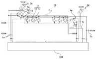
(素子基板10の全体構成)
図2(a)、(b)は、図1に示す液晶装置100の素子基板10の電気的な構成を示すブロック図、およびセンサ駆動用IC103の構成を示すブロック図である。(Overall configuration of element substrate 10)
2A and 2B are a block diagram illustrating an electrical configuration of the
図2(a)に示すように、素子基板10には、画像表示領域1a(右上がりの斜線を付した領域)に相当する領域に複数のデータ線6a(ソース線)および走査線3a(ゲート線)が互いに交差する方向に形成され、これらの配線の交差部分に対応する位置に複数の画素領域1eが構成されている。これらの画素領域1eには、液晶の配向状態を制御するための画素トランジスタ1cがMIS型の半導体素子(薄膜トランジスタ)によって形成され、画素トランジスタ1cのソースにはデータ線6aが電気的に接続し、画素トランジスタ1cのゲートには走査線3aが電気的に接続している。なお、画像表示領域1aの周りには、画素領域1eと同一の構成を備えたダミーの画素領域1e′が形成されている。ここで、データ線6aおよび走査線3aは駆動用IC101、102から延びている。なお、図示を省略するが、素子基板10には、各画素に対して保持容量を形成するための容量線が形成される場合があり、保持容量を前段の走査線3aとの間に構成する場合には容量線は省略される。 As shown in FIG. 2A, the
ここで、素子基板10は基体がガラス基板などの絶縁基板からなり、製造工程中、データ線6aや走査線3aに静電気が侵入すると、静電気によって画素トランジスタ1cが破壊されることがある。例えば、素子基板10に対する成膜時やエッチング時に素子基板10がプラズマに晒された際や、搬送時に素子基板10が搬送アームと接触した際に、素子基板10が静電気を帯び、データ線6aや走査線3aに静電気が侵入することがある。そこで、大型基板から素子基板10として切り出す領域の外周側にガードリング(図示せず
)と称せられる配線を形成しておき、素子基板10上の共通配線VCOMを双方向ダイオード素子Diを介してガードリングと接続するとともに、共通配線VCOMとデータ線6aとの間、および共通配線VCOMと走査線3aとの間に双方向ダイオード素子Diからなる静電保護素子を介挿してある。従って、素子基板10の製造工程中、データ線6aおよび走査線3aに侵入した静電気を双方向ダイオード素子Diを介して共通配線VCOMに逃がすとともに、共通配線VCOMに侵入した静電気を双方向ダイオード素子Diを介してガーリングに逃がすことができる。それ故、素子基板10の製造工程において、画素トランジスタ1cを静電気から保護することができる。なお、液晶装置100に用いられている段階で、ガードリングは素子基板10から切り離されているが、双方向ダイオード素子Diは素子基板10上に残されている。但し、双方向ダイオード素子Diは、後述するように、MIS型の半導体素子1sにおいてドレインとゲートを接続させてなるMIS型ダイオードを2つ、逆向きに並列接続された構造を備えており、しきい値電圧の制御が容易であり、リーク電流も比較的低いので、液晶装置100の段階で素子基板10上に双方向ダイオード素子Diが残っていても表示動作などに支障はない。Here, the base of the
(素子基板10の詳細構成)
図3(a)、(b)は、図1に示す液晶装置100の素子基板10に構成したセンサ素子などの電気的な構成を示すブロック図であり、図3(a)には、素子基板に外部回路を搭載する前の状態を示し、図3(b)には外部回路を搭載した後の構成を示してある。(Detailed configuration of element substrate 10)
FIGS. 3A and 3B are block diagrams showing an electrical configuration of sensor elements and the like configured on the
図2(a)および図3(a)、(b)に示すように、本形態の液晶装置100に用いた素子基板10では、画素表示領域1aの端部(画素領域1eが配置されている領域の端部)には、画素表示領域1aの1辺に沿って、照度などの状態量を検出するための複数のセンサ素子1fを備えたセンサ素子形成領域1xが形成され、このセンサ素子形成領域1xに対して外側には、センサ素子1fによる検出を行う際の比較に用いられる参照用の複数のセンサ素子1f′を備えた参照用センサ素子形成領域1x′が形成されている。これらの領域のうち、センサ素子形成領域1xは外光が届くように形成されている一方、参照用センサ素子形成領域1x′は、対向基板20に形成された遮光膜や、液晶装置100のフレームなどによって覆われ、外光が届かないようになっている。 As shown in FIG. 2A, FIG. 3A, and FIG. 3B, in the
これらのセンサ素子1f、1f′の詳細な構造については、後述するが、いずれも、MIS型の半導体素子1hと、この半導体素子1hに並列に電気的に接続された容量素子1iとによって構成されている。 Although the detailed structure of these
また、素子基板10において、画素領域1eが配置されている領域の端部には、センサ素子1f、1f′の一対のソース・ドレイン電極の一方(ドレイン電極)からの信号出力を行うためのセンサ用信号線1j、1j′が形成されており、センサ用信号線1j、1j′は、センサ駆動用IC103に電気的に接続されている。なお、センサ用信号線1j、1j′は各々、キャパシタからなるノイズフィルタ素子1t、1t′を介して共通配線VCOMに電気的に接続されている。 In the
さらに、素子基板10上には、センサ駆動用IC103からセンサ素子形成領域1x、および参照用センサ素子形成領域1x‘に向けては共通のゲートオフ用配線1mが延びており、このゲートオフ配線1mは、途中で分岐して、センサ素子形成領域1xに形成されているセンサ素子1fのゲート電極、および参照用センサ素子形成領域1x′に形成されている参照用センサ素子1f′のゲート電極に電気的に接続されている。なお、センサ素子1f、1f′の一対のソース・ドレイン電極の他方(ソース電極)には共通配線VCOMが電気的に接続している。
Further, on the
このように構成した素子基板10において、画素領域1eが配置されている領域の端部
では、センサ素子1f、1f′を静電気から保護することを目的に、センサ用信号線1j、1j′と共通配線VCOMとの間に容量結合動作型双方向ダイオード素子1dからなる静電保護素子が介挿されている。また、ゲートオフ用配線1mと共通配線VCOMとの間にも、容量結合動作型双方向ダイオード素子1dからなる静電保護素子が介挿されている。In the
このような容量結合動作型双方向ダイオード素子1dは、その詳細な構造については後述するが、MIS型の半導体素子1yと、この半導体素子1yのゲート電極とソース・ドレイン電極の一方(ドレイン電極)との間に介挿された容量素子1zとにより構成されたMIS型のダイオード素子(容量結合動作型ダイオード素子)が逆向きに並列接続された構成を有している。 The capacitively coupled operation type
また、素子基板10上には、容量結合動作型双方向ダイオード素子1dに対して、半導体素子1yを非導通状態とするゲート電圧をゲート電極に供給するための制御用配線1nが形成されており、この制御用配線1nは、センサ駆動用IC103から延びて半導体素子yのゲート電極に電気的に接続している。 Further, on the
なお、このように構成したセンサ素子1f、1f′に対する信号処理などを行うことを目的に、図2(b)に示すように、センサ駆動用IC103には、CPUなどの制御部103aによる制御の下、センサ素子1f、1f′からの信号出力などを行う入力制御部103xと、センサ素子1f、1f′からの信号出力を処理する信号処理部部103yとが構成されている。ここで、入力制御部103xは、センサ素子1f、1f′からの信号入力を切り替えるスイッチ回路103b、103b′と、スイッチ回路103b、103b′を介して入力されたセンサ出力を増幅するアンプ回路103c、103c′とを備えている。信号処理部部103yは、センサ出力にアナログ−デジタル変換を行うA/Dコンバータ回路103d、103d′と、センサ素1fからの出力と参照用のセンサ素子1f′から出力に減算処理を施す演算回路103eと、この演算回路103eにより得られたセンサ信号をしきい値103gと比較して比較回路103fと、この比較回路103gでの比較結果に基づいて明るさ信号(照度信号)を求めて出力する信号出力部103hとが構成されている。
For the purpose of performing signal processing on the
(画素トランジスタ1cの構成)
図4(a)、(b)は各々、素子基板10に形成された画素領域1eの3つ分の平面図、およびA4−A4′断面図である。図4(a)に示すように、データ線6aと走査線3aとに囲まれた画素領域1eには、ボトムゲート型の薄膜トランンジスタからなる画素トランジスタ1cのチャネル領域を構成する半導体層2aが形成されている。また、走査線3aからの突出部分によってゲート電極3bが形成されている。半導体層2aのうち、ソース側の端部には、データ線6aの一部がソース電極6bとして重なっており、ドレイン側の端部にはドレイン電極6cが重なっている。また、ドレイン電極6cに対しては、画素電極9aがコンタクトホール81を介して電気的に接続している。(Configuration of
FIGS. 4A and 4B are a plan view of three
このように構成した画素トランジスタ1cの断面は、図4(b)に示すように表される。まず、ガラス基板や石英基板からなる絶縁基板11上には、走査線3a(ゲート電極3b)が形成されている。ゲート電極3bの上層側にはゲート絶縁膜4が形成されている。ゲート絶縁膜4の上層のうち、ゲート電極3bと部分的に重なる領域には、画素トランジスタ1cのチャネル領域を構成する半導体層2aが形成されている。半導体層2aのうち、ソース領域の上層には、ドープトシリコン膜からなるオーミックコンタクト層7a、およびソース電極6bが積層され、ドレイン領域の上層には、ドープトシリコン膜からなるオーミックコンタクト層7b、およびドレイン電極6cが積層されている。 The cross section of the
ゲート絶縁膜4は、例えば、シリコン窒化膜からなる。走査線3aは、例えば、アルミニウム合金膜とモリブデン膜との多層膜である。半導体層2aは、例えば、アモルファスシリコン膜からなり、オーミックコンタクト層7a、7bは、例えば、リンがドープされたn+型のアモルファスシリコン膜からなる。データ線6a(ソース電極6b)およびドレイン電極6cはいずれも、例えば、下層側から上層側に向けて、モリブデン膜、アルミニウム膜、およびモリブデン膜を積層した3層構造を備えている。The
ソース電極6bおよびドレイン電極6cの上層側にはパッシベーション膜8(保護膜/層間絶縁膜)が形成されており、パッシベーション膜8は、例えば、シリコン窒化膜からなる。パッシベーション膜8の上層には画素電極9aが形成されており、画素電極9aは、パッシベーション膜8に形成されたコンタクトホール81を介してドレイン電極6cに電気的に接続している。画素電極9aは、例えば、ITO膜(Indium Tin Oxide)からなる。 A passivation film 8 (protective film / interlayer insulating film) is formed on the upper layer side of the
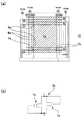
(双方向ダイオード素子Diの構成)
図5(a)、(b)、(c)は各々、素子基板10に形成された双方向ダイオードDiの等価回路図、平面図、およびA5−A5′断面図である。図5(a)、(b)、(c)に示すように、双方向ダイオード素子Diでは、一対のソース・ドレイン電極6d、6e、チャネル領域を備えた半導体層2b、およびチャネル領域にゲート絶縁膜4を介して対向するゲート電極3cを備えたMIS型の半導体素子1sを2つ、互いに逆向きに並列に電気的に接続するとともに、いずれの半導体素子1sにおいても、一対のソース・ドレイン電極のうち、ドレイン電極6eをゲート電極3cに接続した構造を備えている。ここで、一方の半導体素子1sのドレイン電極6e、および他方の半導体素子1sのソース電極6dは、データ線6aあるいは走査線3aに接続され、一方の半導体素子のソース電極6d、および他方の半導体素子のドレイン電極6eは、共通配線VCOMに接続されている。
(Configuration of bidirectional diode element Di)
FIGS. 5A, 5B, and 5C are an equivalent circuit diagram, a plan view, and a sectional view taken along line A5-A5 ′ of the bidirectional diode Di formed on the
このように構成した双方向ダイオード素子Diにおいて、一対の半導体素子1sは同一構造を有しており、これらの半導体素子1sの断面構造を図5(c)を参照して説明する。図5(c)に示すように、双方向ダイオード素子Diにおいて、半導体素子1sでは、画素トランジスタ1cと同様、絶縁基板11上にゲート電極3cが形成され、このゲート電極3cの上層側にはゲート電極3cを覆うようにゲート絶縁膜4が形成されている。ゲート絶縁膜4の上層のうち、ゲート電極3cと部分的に重なる領域には、チャネル領域を備えた半導体層2bが形成されている。半導体層2bの一方の端部には、ドープトシリコン膜からなるオーミックコンタクト層7c、およびソース・ドレイン電極6d、6eのうち、ソース電極6dが積層され、半導体層2bの他方の端部には、ドープトシリコン膜からなるオーミックコンタクト層7d、およびソース・ドレイン電極6d、6eのうち、ドレイン電極6eが積層されている。また、ソース・ドレイン電極6d、6eの上層側にはパッシベーション膜8が形成されている。パッシベーション膜8の上層には、ITO膜からなる中継電極9bが形成され、この中継電極9bは、パッシベーション膜8に形成されたコンタクトホール82を介してゲート電極3cに電気的に接続し、パッシベーション膜8およびゲート絶縁膜4に形成されたコンタクトホール83を介してドレイン電極6eに電気的に接続している。
In the bidirectional diode element Di configured as described above, the pair of
ここで、双方向ダイオード素子Diと画素トランジスタ1cとは、ソース・ドレイン電極同士、半導体層同士、およびゲート電極同士が同一の層間に同一材料により形成され、中継電極9bは画素電極9aと同一の層上に同一材料により形成されており、双方向ダイオード素子Diおよび画素トランジスタ1cについては共通の工程によって形成することができる。 Here, in the bidirectional diode element Di and the
(容量結合動作型双方向ダイオード素子1dの構成)
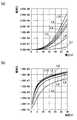
図6(a)、(b)、(c)は各々、素子基板10に形成された容量結合動作型双方向ダイオード素子1dの等価回路図、平面図、およびA6−A6′断面図である。図7(a)、(b)は、図6に示す容量結合動作型双方向ダイオード素子、および図5に示す双方向ダイオード素子のI−V特性を示すグラフ、およびその結果を対数スケールで表示したグラフである。(Configuration of Capacitively Coupled Operation Type
6A, 6B, and 6C are an equivalent circuit diagram, a plan view, and a sectional view taken along line A6-A6 'of the capacitively coupled
図6(a)、(b)、(c)に示すように、容量結合動作型双方向ダイオード素子1dでは、一対のソース・ドレイン電極6f、6g、チャネル領域を備えた半導体層2c、およびチャネル領域にゲート絶縁膜4を介して対向するゲート電極3dを備えたMIS型の半導体素子1yを2つ、互いに逆向きに電気的に接続するとともに、いずれの半導体素子1yにおいても、一対のソース・ドレイン電極6f、6gのうち、ドレイン電極6gとゲート電極3dとの間に容量素子1zが介挿された構造を備えている。ここで、2つの半導体素子1yのうち、一方の半導体素子のドレイン電極6g、および他方の半導体素子のソース電極6fは、センサ用信号線1j、1j′、およびゲートオフ配線1mに接続され、一方の半導体素子のソース電極6f、および他方の半導体素子のドレイン電極6gは、共通配線VCOMに接続されている。
As shown in FIGS. 6A, 6B and 6C, in the capacitively coupled
また、図6(b)に示すように、2つの半導体素子1yのいずれにおいても、ゲート電極3dには、半導体素子1yを非導通状態とするための制御用配線1nが電気的に接続されている。 Further, as shown in FIG. 6B, in any of the two
このように構成した容量結合動作型双方向ダイオード素子1dにおいて、一対の半導体素子1yは同一構造を有しており、これらの半導体素子1yの断面構造を図6(c)を参照して説明する。図6(c)に示すように、容量結合動作型双方向ダイオード素子1dにおいて、半導体素子1yでは、画素トランジスタ1cと同様、絶縁基板11上にゲート電極3dが形成され、このゲート電極3dの上層側にはゲート電極3dを覆うようにゲート絶縁膜4が形成されている。ゲート絶縁膜4の上層のうち、ゲート電極3dと部分的に重なる領域には、チャネル領域を備えた半導体層2cが形成されている。半導体層2cの一方の端部には、ドープトシリコン膜からなるオーミックコンタクト層7e、およびソース・ドレイン電極6f、6gのうち、ソース電極6fが積層され、半導体層2cの他方の端部には、ドープトシリコン膜からなるオーミックコンタクト層7f、およびソース・ドレイン電極6f、6gのうち、ドレイン電極6gが積層されている。また、ソース・ドレイン電極6f、6gの上層側にはパッシベーション膜8が形成されている。 In the capacitively coupled
さらに、ゲート電極3dの延設部分によって下電極3eが形成され、この下電極3eに対しては、ゲート絶縁膜4を介して、ドレイン電極6gからの延設部分が上電極6hとして対向し、容量素子1zが構成されている。 Further, a
ここで、容量結合動作型双方向ダイオード素子1dと、双方向ダイオード素子Diおよび画素トランジスタ1cとは、ソース・ドレイン電極同士、半導体層同士、およびゲート電極同士が同一の層間に同一材料により形成されており、容量結合動作型双方向ダイオード素子1d、双方向ダイオード素子Diおよび画素トランジスタ1cについては共通の工程によって形成することができる。 Here, the capacitively coupled
このような容量結合動作型双方向ダイオード素子1dでは、ゲート電極3dとソース電極6fとの間、およびゲート電極3dとドレイン電極6gとの間に寄生容量Csが発生している場合でも急峻なI−V特性が得られる。すなわち、図7(a)、(b)には、容量結合動作型双方向ダイオード素子1dにおける対寄生容量比k(=容量素子1zの容量CL/寄生容量Cs)を変化させた場合のI−V特性と、図5に示した双方向ダイオード素子DiのI−V特性を比較して示してある。図7(a)、(b)において、線L1、線L2、線L3、線L4、線L5で示す特性は、容量結合動作型双方向ダイオード素子1dにおける対寄生容量比kが1、2、5、10、20の場合のI−V特性を示し、線L10で示す特性は、図5に示した双方向ダイオード素子DiのI−V特性を示す。
In such capacitive coupling-operation
図7(a)、(b)に示すように、容量結合動作型双方向ダイオード素子1dでは、対寄生容量比kが上昇するに伴ってI−V特性が急峻となり、特に、対寄生容量比kが5以上の場合には、図5に示した双方向ダイオード素子Diと同様、十分に急峻なI−V特性が得られる。すなわち、対寄生容量比kが5以上の場合には、ゲート電極3dとドレイン電極6gとを直接、接続しなくても、十分に急峻なI−V特性が得られる。これは、容量結合動作型双方向ダイオード素子1dの両端に印加された電圧をVとし、寄生容量Csに加わる電圧をV(Cs)とし、容量素子1zに加わる電圧をV(CL)とした場合に、印加された電圧Vが、以下の式
V=V(Cs)+V(CL)
V(Cs)=(CL/(Cs+CL))×V
V(CL)=(Cs/(Cs+CL))×V
V(Cs)<V(CL)
で示すように、寄生容量Csおよび容量素子1zに容量分割される結果、対寄生容量比kが5以上の場合、容量結合動作型双方向ダイオード素子1dのI−V特性が、図5に示した双方向ダイオード素子DiのI−V特性に近づくものと解釈できる。従って、容量結合動作型双方向ダイオード素子1dは、静電気などといった高い電圧が印加された場合には、静電保護素子として機能する。また、容量結合動作型双方向ダイオード素子1dは、図5に示した双方向ダイオード素子Diと比較して、中継電極による接続を不要としない分、製造工程の比較的早い時期に完成し、それ以降に発生した静電気を逃がすので、製造工程の比較的早い時期からセンサ素子1f、1f′を静電気から保護することができる。As shown in FIGS. 7A and 7B, in the capacitively coupled operation type
V (Cs) = (CL / (Cs + CL)) × V
V (CL) = (Cs / (Cs + CL)) × V
V (Cs) <V (CL)
As shown in FIG. 5, when the parasitic capacitance ratio k is 5 or more as a result of the capacitive division into the parasitic capacitance Cs and the
しかも、容量結合動作型双方向ダイオード素子1dでは、2つの半導体素子1yのいずれにおいても、ゲート電極3dには、半導体素子1yを非導通状態とするための制御用配線1nが電気的に接続されているため、制御用配線1nを介してゲート電極3dにオフ電圧を印加すれば、2つの半導体素子1yのいずれをも完全に非導通状態とすることができる。 In addition, in the capacitively coupled operation type
(センサ素子1f、1fの構成)
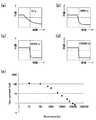
図8(a)、(b)、(c)は各々、素子基板10に形成されたセンサ素子1f、1f′の等価回路図、平面図、およびA8−A8′断面図である。図9は、図8に示すセンサ素子における放電特性およびその時定数と照度との関係を示すグラフである。図8(a)、(b)、(c)に示すように、センサ素子1f、1f′は、一対のソース・ドレイン電極6i、6j、チャネル領域を備えた半導体層2d、およびチャネル領域にゲート絶縁膜4を介して対向するゲート電極3fを備えたMIS型の半導体素子1hと、半導体素子1hと並列に電気的に接続された容量素子1iとを備えている。ここで、半導体素子1hのドレイン電極6jは、センサ用信号線1j、1j′に接続され、ソース電極6iは、共通配線VCOMに接続されている。また、ゲート電極3fに対して、半導体素子1hを非導通状態とするためのゲートオフ配線1mが電気的に接続されている。(Configuration of
FIGS. 8A, 8B, and 8C are an equivalent circuit diagram, a plan view, and a sectional view taken along line A8-A8 ′ of
このように構成したセンサ素子1f、1f′の断面構造を図8(c)を参照して説明する。図8(c)に示すように、センサ素子1f、1f′において、半導体素子1hでは、画素トランジスタ1cと同様、絶縁基板11上にゲート電極3fが形成され、このゲート電極3fの上層側にはゲート電極3fを覆うようにゲート絶縁膜4が形成されている。ゲート絶縁膜4の上層のうち、ゲート電極3fと部分的に重なる領域には、チャネル領域を備えた半導体層2dが形成されている。半導体層2dの一方の端部には、ドープトシリコ
ン膜からなるオーミックコンタクト層7g、およびソース・ドレイン電極6i、6jのうち、ソース電極6iが積層され、半導体層2dの他方の端部には、ドープトシリコン膜からなるオーミックコンタクト層7h、およびソース・ドレイン電極6i、6jのうち、ドレイン電極6jが積層されている。また、ソース・ドレイン電極6i、6jの上層側にはパッシベーション膜8が形成されている。A cross-sectional structure of the
さらに、ゲート電極3fの側方には、島状の下電極3gがゲート電極3fと同時形成されており、この島状の下電極3gに対しては、ドレイン電極6jから延設された上電極6kが対向している。また、下電極3gに重なる位置にはゲート絶縁膜4およびパッシベーション膜8を貫通するコンタクトホール85が形成され、ソース電極6iと重なる位置にはパッシベーション膜8を貫通するコンタクトホール84が形成されている。さらに、パッシベーション膜8の上層にはITO膜からなる中継電極9cが形成されており、中継電極9cは、コンタクトホール84、85を介してソース電極6iおよび下電極3gに電気的に接続している。
Further, an island-shaped
ここで、センサ素子1f、1f‘は、画素トランジスタ1c、双方向ダイオード素子Diおよび容量結合動作型双方向ダイオード素子1dと、ソース・ドレイン電極同士、半導体層同士、およびゲート電極同士が同一の層間に同一材料により形成され、中継電極9cは画素電極9aおよび中継電極9bと同一の層上に同一材料により形成されており、センサ素子1f、1f‘、画素トランジスタ1c、双方向ダイオード素子Diおよび容量結合動作型双方向ダイオード素子1dについては、共通の製造工程によって形成することができる。
Here, the
このように構成したセンサ素子1f、1f′では、照度を検出する際、図8(a)に示すように、ゲートオフ配線1mを介してゲート電極3fに例えば−10Vのゲート電圧を印加して半導体素子1hをオフ状態にした状態で、センサ用信号線1j、1j′を介してソース・ドレイン電極6i、6j間に、例えば+2Vを印加して容量素子1iに充電を行う。次に、センサ用信号線1j、1j′を介してのソース・ドレイン電極6i、6jへの給電を停止する。その結果、センサ用信号線1j、1j′からは、センサ素子1f、1f′の端子間電圧が出力される。ここで、端子間電圧の変化は、容量素子1iに充電された際の電荷が、半導体素子1hを介して放電する際の放電曲線を示し、かつ、半導体素子1hを介しての放電は、半導体素子1hが受けた光量で変化する。例えば、図9(a)、(b)、(c)、(d)に照度が10lx、10000lx、50000lx、150000lxにおける放電特性を示すように、照度が高いほど放電が急峻に起こり、図9(e)に示すように、照度が高いほど放電時の時定数が小さい。それ故、時定数を求めれば、照度を検出できることになる。 In the
(製造方法)
このように構成した液晶装置100を製造するにあたっては、周知の半導体プロセスなどを適用すればよいので、詳細な説明は省略するが、絶縁基板11上にゲート電極3bや走査線3aを形成した後、ゲート絶縁膜4、半導体層2a、オーミックコンタクト層7a、7b、ソース・ドレイン電極6b、6cを形成する。その時点で、画素トランジスタ1c、およびセンサ素子1f、1f′の半導体素子1fが完成するとともに、容量結合動作型双方向ダイオード素子1dも完成する。従って、それ以降、センサ用信号線1j、1j′およびゲートオフ配線1mに静電気が侵入した場合でも、静電気を容量結合動作型双方向ダイオード素子1dを介して共通配線VCOMに逃がすことができるので、センサ素子1fを静電気から保護することができる。
(Production method)
In manufacturing the
そして、パッシベーション膜8や画素電極9aを形成した時点では双方向ダイオードDiが完成するので、それ以降、データ線6aおよび走査線3aに静電気が侵入した場合でも、静電気を双方向ダイオード素子Diを介して共通配線VCOMに逃がすことができる
ので、画素トランジスタ1cを静電気から保護することができる。このようにして素子基板10を製造した後、素子基板10と対向基板20とをシール52を介して貼り合せ、その間に液晶50を充填する。Since the bidirectional diode Di is completed when the
次に、素子基板10に対して駆動用IC101、102を実装するとともに、センサ駆動用IC103が実装されたフレキシブル配線基板105を素子基板10に接続すると、液晶装置100が完成する。そして、液晶装置100を携帯電話などの電子機器に搭載する。 Next, when the driving
(製造方法)
(センシング動作)
このような電子機器を使用する際、液晶装置100では画像が表示されるとともに、その際の条件は、センサ素子1f、1f′によって検出された照度に応じて最適化される。すなわち、液晶装置100では、センサ駆動用IC103からゲートオフ配線1mを介してセンサ素子1f、1f′のゲート電極3fに対して、半導体素子1fをオフ状態とするゲート電圧、例えば−10Vを印加するとともに、センサ用信号線1j、1j′を介してセンサ素子1f、1f‘に定電圧、例えば+2Vを供給して容量素子1iを充電する。次に、センサ用信号線1j、1j′を介してのセンサ素子1f、1f′への定電圧の供給を停止すると、センサ素子1f、1f′からは、センサ用信号線1j、1j′を介してセンサ駆動用IC103に対してセンサ素子1f、1f′の端子間電圧変化(放電曲線)が出力され、その出力結果に基づいて時定数を求めると、照度を求めることができる。従って、照度の検出結果を例えばバックライト装置にフィードバックすると、周囲の照度に適した条件での表示を行うことができる。例えば、周囲の照度が高い場合にはその分、バックライト装置からの出射強度を高めて明るい表示を行う一方、周囲の照度が低い場合にはその分、バックライト装置からの出射強度を低くする。また、照度の検出結果に基づいて、画像の諧調を規定する信号レベルを最適化してもよい。このような液晶装置100での照度の検出は、電子機器が使用されている間、予め設定された時間間隔で、あるいは利用者によるボタン操作などにより行われる。
(Production method)
(Sensing operation)
When such an electronic apparatus is used, an image is displayed on the
その間、容量結合動作型双方向ダイオード素子1dに用いた2つの半導体素子1yのゲート電極3dには、制御用配線1nを介して、半導体素子1yを非導通状態とするためのゲート電圧が印加されるため、容量結合動作型双方向ダイオード素子1dについては、センサ用信号線1j、1j′から電気的に分離することができる。 Meanwhile, a gate voltage for turning off the
(本形態の主な効果)
以上説明したように、本形態の液晶装置100では、素子基板10上にセンサ素子1f、1f′が形成されているため、センサ素子1f、1f′によって、液晶装置100が置かれた環境での照度を検出し、照度に対応した条件で画像表示を行うことができる。(Main effects of this form)
As described above, in the
また、素子基板10の製造中、センサ素子1f、1f‘から信号出力を行うセンサ用信号線1j、1j′およびゲートオフ配線1mは、容量結合動作型双方向ダイオード素子1dを介して共通配線VCOMに電気的に接続されているので、電気光学装置の製造途中などおいて素子基板10に静電気が侵入した場合でも、かかる静電気を容量結合動作型双方向ダイオード素子1dを介して共通配線VCOMに逃がすことができ、センサ素子1f、1f′を静電気から保護することができる。Further, during the manufacture of the
ここで、センサ用信号線1j、1j′およびゲートオフ配線1mに接続する容量結合動作型双方向ダイオード素子1dは、半導体素子1yのドレイン電極6gとゲート電極3dとの間に容量素子1zが介挿された構造になっているので、静電気に起因する高い電圧がセンサ用信号線1j、1j′と共通配線VCOMとの間に発生した場合には寄生容量Csと容量素子1zとの容量結合により半導体素子1yが導通状態になり、静電気を逃がすこ
とができる。また、容量結合動作型双方向ダイオード素子1dは、図5を参照して説明した双方向ダイオード素子と比較して、製造工程の比較的早い時期に完成し、それ以降に発生した静電気を逃がすので、製造工程の比較的早い時期からセンサ素子1f、1f′を静電気から保護することができる。Here, in the capacitively coupled
さらに、容量結合動作型双方向ダイオード素子1dを構成する半導体素子1yのゲート電極3dに対しては制御用配線1nが形成されているため、制御用配線1nからゲート電極3dに所定のゲート電圧を印加すれば、容量結合動作型双方向ダイオード素子1dを確実に非導通状態とすることができるので、容量結合動作型双方向ダイオード素子1dは、センサ素子1f、1f′から出力される信号に影響を及ぼさない。それ故、素子基板10上に形成したセンサ用信号線1j、1j′を双方向ダイオード素子Diを介して共通配線VCOMに電気的に接続して静電気からセンサ素子1f、1f′を保護する構成を採用した場合でも、センサ素子1fによる検出を高い精度で行うことができる。 Further, since the
[他の実施の形態]
図10および図11は、本発明を適用した別の素子基板10の電気的な構成を示すブロック図、およびこの素子基板に構成したセンサ素子などの電気的な構成を示すブロック図である。なお、本形態の基本的な構成は、図3および図4などを参照して説明した実施の形態と同様であるため、共通する部分には同一の符号を付して図示し、それらの説明を省略する。[Other embodiments]
FIG. 10 and FIG. 11 are a block diagram showing an electrical configuration of another
図10に示すように、本形態の液晶装置に用いた素子基板10でも、画像表示領域1a(右上がりの斜線を付した領域)に相当する領域に複数のデータ線6a(ソース線)および走査線3a(ゲート線)が互いに交差する方向に形成され、これらの配線の交差部分に対応する位置に複数の画素領域1eが構成されている。これらの画素領域1eには、液晶の配向状態を制御するための画素トランジスタ1cがMIS型の半導体素子(薄膜トランジスタ)によって形成されている。また、素子基板10は基体がガラス基板などの絶縁基板からなり、製造工程中、データ線6aや走査線3aに静電気が侵入すると、静電気によって画素トランジスタ1cが破壊されることがあるので、素子基板10上の共通配線VCOMを、図5を参照して説明した双方向ダイオード素子Diを介してガードリング(図示せず)と接続するとともに、共通配線VCOMとデータ線6aとの間、および共通配線VCOMと走査線3aとの間には双方向ダイオード素子Diからなる静電保護素子が介挿されている。 As shown in FIG. 10, even in the
本形態でも、素子基板10では、画素表示領域1aの縁に沿って、複数のセンサ素子1fを備えたセンサ素子形成領域1xが形成されている。但し、本形態では、センサ素子1fによって温度を検出するため、参照用のセンサ素子は形成されていない。センサ素子1fは、図8を参照して説明したように、MIS型の半導体素子1hと、この半導体素子1hに並列に電気的に接続された容量素子1iとによって構成されている。また、素子基板10上には、センサ素子1fの一対のソース・ドレイン電極の一方(ドレイン電極)からの信号出力を行うためのセンサ用信号線1jが形成されており、センサ用信号線1jは、センサ駆動用IC103に電気的に接続されている。なお、センサ用信号線1jは各々、キャパシタからなるノイズフィルタ素子1tを介して共通配線VCOMに電気的に接続されている。さらに、素子基板10上には、センサ駆動用IC103からセンサ素子形成領域1xに向けてゲートオフ用配線1mが延びており、このゲートオフ配線1mは、センサ素子1fのゲート電極に電気的に接続されている。なお、センサ素子1fの一対のソース・ドレイン電極の他方(ソース電極)には共通配線VCOMが電気的に接続している。さらにまた、素子基板10では、センサ素子1fを静電気から保護することを目的に、センサ用信号線1jおよびゲートオフ配線1mと共通配線VCOMとの間には、容量結合動作型双方向ダイオード素子1dからなる静電保護素子が介挿されている。このような容量結
合動作型双方向ダイオード素子1dは、MIS型の半導体素子1yと、この半導体素子1yのゲート電極とドレイン電極との間に並列接続された容量素子1zとにより構成されたMIS型のダイオード素子が逆向きに並列接続された構成を有している。また、素子基板10上には、容量結合動作型双方向ダイオード素子1dに対して、半導体素子1yを非導通状態とするゲート電圧をゲート電極に供給するための制御用配線1nが形成されており、この制御用配線1nは、センサ駆動用IC103から延びて半導体素子1yのゲート電極に電気的に接続している。Also in this embodiment, in the
このように構成した液晶装置では、センサ素子1fによって、液晶装置100が置かれた環境の温度を検出し、温度に対応した条件で画像表示を行うことができる。また、素子基板10の製造中、素子基板10に静電気が侵入した場合でも、かかる静電気を容量結合動作型双方向ダイオード素子1dを介して共通配線VCOMに逃がすことができ、センサ素子1fを静電気から保護することができる。さらに、容量結合動作型双方向ダイオード素子1dを構成する半導体素子1yのゲート電極3dに対しては制御用配線1nが形成されているため、制御用配線1nからゲート電極3dに所定のゲート電圧を印加すれば、容量結合動作型双方向ダイオード素子1dを確実に非導通状態とすることができるので、容量結合動作型双方向ダイオード素子1dは、センサ素子1fから出力される信号に影響を及ぼさない。それ故、素子基板10上に形成したセンサ用信号線1jを双方向ダイオード素子Diを介して共通配線VCOMに電気的に接続して静電気からセンサ素子1fを保護する構成を採用した場合でも、センサ素子1fによる検出を高い精度で行うことができる。 In the liquid crystal device configured as described above, the temperature of the environment where the
[その他の実施の形態]
上記実施の形態では、透過型の液晶装置100を例に説明したが、全反射型の液晶装置や半透過反射型の液晶装置に本発明を適用してもよい。また、上記実施の形態では、走査線などにアルミニウム合金膜とモリブデン膜との多層膜を用い、データ線にアルミニウム膜とモリブデン膜との多層膜を用いたが、これらの配線にはその他の金属膜を用いることができ、さらには、シリサイド膜などといった導電膜を用いてもよい。また、上記実施の形態では半導体層として真性のアモルファスシリコン膜を用いたが、その他のシリコン膜を用いてもよい。[Other embodiments]
In the above embodiment, the transmissive
また、 また、上記実施の形態では、TNモード、ECBモード、VANモードのアクティブマトリクス型の液晶装置100を例に説明したが、IPS(In−Plane Switching)モードの液晶装置100(電気光学装置)に本発明を適用してもよい。 In the above embodiment, the TN mode, ECB mode, and VAN mode active matrix type
さらに、電気光学装置として液晶装置100に限らず、例えば、有機EL(エレクトロルミネッセンス)装置や撮像装置でも、素子基板10上に互いに交差して延びた複数のデータ線および複数の走査線と、データ線と走査線との交差部に対応して構成された画素領域とを有するので、本発明を適用してもよい。 Further, the electro-optical device is not limited to the
[電子機器の実施形態]
図12は、本発明に係る液晶装置を備えた電子機器の説明図である。本発明を適用した液晶装置100は、例えば、図12(a)に示す携帯電話1000、図12(b)に示すページャ1100、図12(c)に示すモバイルコンピュータ1200に搭載することができ、これらの場合、液晶装置100は、これらの電子機器において表示部1001、1101、1201を構成する。このような電子機器は、屋外で使用されることが多いが、本発明を適用して液晶装置100を用いれば、かかる使用環境に応じた条件での表示が可能である。なお、本発明を適用した液晶装置100は、その他にも、ディジタルスチルカメラ、液晶テレビ、ビューファインダ型あるいはモニタ直視型のビデオテープレコーダ、
カーナビゲーション装置、電子手帳、電卓、ワードプロセッサ、ワークステーション、テレビ電話、POS端末、タッチパネルを備えた電子機器などに対して表示装置として搭載される。[Embodiment of Electronic Device]
FIG. 12 is an explanatory diagram of an electronic apparatus including the liquid crystal device according to the present invention. The
It is mounted as a display device on car navigation devices, electronic notebooks, calculators, word processors, workstations, video phones, POS terminals, electronic devices equipped with touch panels, and the like.
1a・・画像表示領域、1c・・画素トランジスタ、1d・・容量結合動作型双方向ダイオード素子、1f・・センサ素子、1j・・センサ用信号線、1m・・ゲートオフ配線、1n・・制御用配線、3a・・走査線、6a・・データ線、9a・・画素電極、10・・素子基板、20・・対向基板、100・・液晶装置、101、102・・駆動用IC、103・・センサ駆動用IC、Di・・双方向ダイオード素子、VCOM・・共通配線1a..Image display area, 1c..Pixel transistor, 1d..Capacitive coupling operation type bidirectional diode element, 1f..Sensor element, 1j..Signal line for sensor, 1m..Gate off wiring, 1n..For control Wiring, 3a ... Scanning line, 6a ... Data line, 9a ... Pixel electrode, 10 ... Element substrate, 20 ... Counter substrate, 100 ... Liquid crystal device, 101, 102 ... Driving IC, 103 ... IC for sensor drive, Di ... Bidirectional diode element, VCOM ... Common wiring
Claims (9)
Translated fromJapanese前記素子基板には、
センサ素子と、
該センサ素子から信号出力を行うセンサ用信号線と、
共通配線と、
ソース電極、ドレイン電極、チャネル領域を備えた半導体層、および当該チャネル領域にゲート絶縁膜を介して対向するゲート電極を有する半導体素子と、前記ソース電極および前記ドレイン電極のうちの一方と前記ゲート電極との間に介挿された容量素子と、を備えた2つの容量結合動作型ダイオード素子を互いに逆向きに電気的に接続した容量結合動作型双方向ダイオード素子と、が形成され、
前記センサ用信号線は、前記容量結合動作型双方向ダイオード素子を介して前記共通配線に電気的に接続され、
前記容量結合動作型双方向ダイオード素子に対しては、前記半導体素子を非導通状態とするゲート電圧を前記ゲート電極に供給するための制御用配線が形成されていることを特徴とする電気光学装置。In an electro-optical device includingan element substrate formed with a plurality of data lines, a plurality of scanning lines, and a plurality of pixel transistors connected to the plurality of scanning lines and the plurality of scanning lines ,
In the element substrate,
A sensor element;
A sensor signal line for outputting a signal from the sensor element;
Common wiring,
A semiconductor element having a source electrode, a drain electrode, a semiconductor layer including a channel region, and a gate electrode facing the channel region with a gate insulating film interposed therebetween; and one of the source electrode and the drain electrode and the gate electrode A capacitive coupling operation type bidirectional diode element in which two capacitive coupling operation type diode elements having a capacitance element interposed between and are electrically connected in opposite directions to each other are formed,
The sensor signal line is electrically connected to the common wiring through the capacitively coupled operation bidirectional diode element,
An electro-optical device for forming a control voltage for supplying to the gate electrode a gate voltage that makes the semiconductor element non-conductive with respect to the capacitively coupled operation type bidirectional diode element. .
当該画素トランジスタと前記容量結合動作型双方向ダイオード素子とは、ソース電極同士、ドレイン電極同士、半導体層同士、およびゲート電極同士が同一の層間に同一材料により形成されていることを特徴とする請求項1乃至7の何れか一項に記載の電気光学装置。Thepixel transistor includes a semiconductor layer including a source electrode, a drain electrode, and a channel region, and a gate electrode facing the channel region through a gate insulating film, and the pixel transistor is electrically connected to the pixel electrode. And
The pixel transistor and the capacitively coupled bidirectional diode element are characterized in that source electrodes, drain electrodes, semiconductor layers, and gate electrodes are formed of the same material between the same layers. Item 8. The electro-optical device according to any one of Items 1 to 7.
Priority Applications (2)
| Application Number | Priority Date | Filing Date | Title |
|---|---|---|---|
| JP2006153106AJP4142066B2 (en) | 2006-06-01 | 2006-06-01 | Electro-optical device and electronic apparatus |
| US11/785,219US7569885B2 (en) | 2006-06-01 | 2007-04-16 | Electro-optical device and electronic apparatus |
Applications Claiming Priority (1)
| Application Number | Priority Date | Filing Date | Title |
|---|---|---|---|
| JP2006153106AJP4142066B2 (en) | 2006-06-01 | 2006-06-01 | Electro-optical device and electronic apparatus |
Publications (2)
| Publication Number | Publication Date |
|---|---|
| JP2007324375A JP2007324375A (en) | 2007-12-13 |
| JP4142066B2true JP4142066B2 (en) | 2008-08-27 |
Family
ID=38790768
Family Applications (1)
| Application Number | Title | Priority Date | Filing Date |
|---|---|---|---|
| JP2006153106AActiveJP4142066B2 (en) | 2006-06-01 | 2006-06-01 | Electro-optical device and electronic apparatus |
Country Status (2)
| Country | Link |
|---|---|
| US (1) | US7569885B2 (en) |
| JP (1) | JP4142066B2 (en) |
Families Citing this family (16)
| Publication number | Priority date | Publication date | Assignee | Title |
|---|---|---|---|---|
| JP5080172B2 (en)* | 2007-08-23 | 2012-11-21 | 富士フイルム株式会社 | Image detection device |
| CN100566168C (en)* | 2008-02-25 | 2009-12-02 | 友达光电股份有限公司 | Bidirectional control device for improving voltage tolerance of assembly |
| CN102160103B (en) | 2008-09-19 | 2013-09-11 | 株式会社半导体能源研究所 | Display device |
| KR101614900B1 (en)* | 2009-10-27 | 2016-04-25 | 삼성디스플레이 주식회사 | Display panel |
| JP5724623B2 (en)* | 2011-05-23 | 2015-05-27 | ソニー株式会社 | Signal transmission device and imaging display system |
| KR101316812B1 (en)* | 2012-02-22 | 2013-10-23 | 주식회사 넥스트아이 | A inspecting apparatus of LCD panel |
| CN104769691A (en)* | 2012-11-02 | 2015-07-08 | 罗姆股份有限公司 | Chip capacitors, circuit components, and electronic equipment |
| KR102483956B1 (en) | 2016-03-31 | 2023-01-03 | 삼성디스플레이 주식회사 | Display device |
| US10147718B2 (en)* | 2016-11-04 | 2018-12-04 | Dpix, Llc | Electrostatic discharge (ESD) protection for the metal oxide medical device products |
| JP2018107161A (en)* | 2016-12-22 | 2018-07-05 | ソニーセミコンダクタソリューションズ株式会社 | Imaging panel, method of manufacturing imaging panel, roentgen device, and imaging device |
| JP6298144B2 (en)* | 2016-12-23 | 2018-03-20 | 株式会社半導体エネルギー研究所 | Semiconductor device |
| JP6703794B2 (en)* | 2018-06-29 | 2020-06-03 | 双葉電子工業株式会社 | Touch panel drive device, touch panel device, touch panel drive method |
| GB2576950B (en) | 2018-09-10 | 2022-03-02 | Pragmatic Printing Ltd | Electronic circuit and method of manufacture |
| CN110518048B (en)* | 2019-08-30 | 2022-04-08 | 武汉天马微电子有限公司 | Display panels and display devices |
| JP7302417B2 (en) | 2019-10-02 | 2023-07-04 | セイコーエプソン株式会社 | Temperature sensing circuits, electro-optical devices and electronics |
| US12148401B2 (en)* | 2021-06-23 | 2024-11-19 | Beijing Boe Optoelectronics Technology Co., Ltd. | Display substrate, display device and compensation method thereof |
Family Cites Families (5)
| Publication number | Priority date | Publication date | Assignee | Title |
|---|---|---|---|---|
| JP3183390B2 (en)* | 1995-09-05 | 2001-07-09 | キヤノン株式会社 | Photoelectric conversion device and imaging device using the same |
| JP3667548B2 (en)* | 1998-03-27 | 2005-07-06 | シャープ株式会社 | Active matrix type liquid crystal display panel and inspection method thereof |
| WO2003023752A1 (en)* | 2001-09-07 | 2003-03-20 | Matsushita Electric Industrial Co., Ltd. | El display, el display driving circuit and image display |
| JP2004303925A (en) | 2003-03-31 | 2004-10-28 | Canon Inc | Imaging board |
| JP2007241358A (en)* | 2006-03-06 | 2007-09-20 | Hitachi Displays Ltd | Image display device |
- 2006
- 2006-06-01JPJP2006153106Apatent/JP4142066B2/enactiveActive
- 2007
- 2007-04-16USUS11/785,219patent/US7569885B2/enactiveActive
Also Published As
| Publication number | Publication date |
|---|---|
| US7569885B2 (en) | 2009-08-04 |
| US20070281430A1 (en) | 2007-12-06 |
| JP2007324375A (en) | 2007-12-13 |
Similar Documents
| Publication | Publication Date | Title |
|---|---|---|
| JP4211805B2 (en) | Electro-optical device and electronic apparatus | |
| JP4142066B2 (en) | Electro-optical device and electronic apparatus | |
| US8722448B2 (en) | Method for fabricating photo detector | |
| US9791991B2 (en) | Display device with a built-in touch panel | |
| KR101675844B1 (en) | Liquid Crystal Display Panel Associated with Touch Panel and Method for Manufacturing the Same | |
| KR101281830B1 (en) | Liquid crystal display having multi-touch sensing function and driving method thereof | |
| US10656476B2 (en) | Liquid crystal panel | |
| KR102018740B1 (en) | Display having touch sensing function | |
| US10034374B2 (en) | Display device | |
| US7999265B2 (en) | Photoelectric conversion device, electro-optic device, and electronic device | |
| US20240061293A1 (en) | Display device | |
| US10921664B2 (en) | Substrate including semiconductors arranged in a matrix and a display device | |
| US9880431B2 (en) | Display device | |
| US12169331B2 (en) | Display device with touch sensors and its wiring | |
| US20140125881A1 (en) | Touch display panel and touch display device using the same | |
| JP5207824B2 (en) | Electro-optical device and electronic apparatus | |
| US10571753B2 (en) | Liquid crystal panel | |
| KR20180079599A (en) | Array Substrate For Display Device And Method Of Fabricating The Same | |
| JP2008083322A (en) | Display device with input function | |
| US11137849B2 (en) | Touch display device and manufacturing method thereof | |
| JP2014123171A (en) | Input device and display device including the input device | |
| JP2008185868A (en) | Electro-optical device | |
| JP2008241511A (en) | Optical detector and electro-optical apparatus | |
| US20220187649A1 (en) | Electronic device and related display device | |
| JP2008186882A (en) | Photodetector and electro-optic device |
Legal Events
| Date | Code | Title | Description |
|---|---|---|---|
| A977 | Report on retrieval | Free format text:JAPANESE INTERMEDIATE CODE: A971007 Effective date:20080428 | |
| TRDD | Decision of grant or rejection written | ||
| A01 | Written decision to grant a patent or to grant a registration (utility model) | Free format text:JAPANESE INTERMEDIATE CODE: A01 Effective date:20080513 | |
| A01 | Written decision to grant a patent or to grant a registration (utility model) | Free format text:JAPANESE INTERMEDIATE CODE: A01 | |
| A61 | First payment of annual fees (during grant procedure) | Free format text:JAPANESE INTERMEDIATE CODE: A61 Effective date:20080611 | |
| FPAY | Renewal fee payment (event date is renewal date of database) | Free format text:PAYMENT UNTIL: 20110620 Year of fee payment:3 | |
| R150 | Certificate of patent or registration of utility model | Ref document number:4142066 Country of ref document:JP Free format text:JAPANESE INTERMEDIATE CODE: R150 | |
| FPAY | Renewal fee payment (event date is renewal date of database) | Free format text:PAYMENT UNTIL: 20110620 Year of fee payment:3 | |
| S111 | Request for change of ownership or part of ownership | Free format text:JAPANESE INTERMEDIATE CODE: R313113 | |
| FPAY | Renewal fee payment (event date is renewal date of database) | Free format text:PAYMENT UNTIL: 20110620 Year of fee payment:3 | |
| R360 | Written notification for declining of transfer of rights | Free format text:JAPANESE INTERMEDIATE CODE: R360 | |
| FPAY | Renewal fee payment (event date is renewal date of database) | Free format text:PAYMENT UNTIL: 20110620 Year of fee payment:3 | |
| S111 | Request for change of ownership or part of ownership | Free format text:JAPANESE INTERMEDIATE CODE: R313113 | |
| FPAY | Renewal fee payment (event date is renewal date of database) | Free format text:PAYMENT UNTIL: 20110620 Year of fee payment:3 | |
| R350 | Written notification of registration of transfer | Free format text:JAPANESE INTERMEDIATE CODE: R350 | |
| FPAY | Renewal fee payment (event date is renewal date of database) | Free format text:PAYMENT UNTIL: 20110620 Year of fee payment:3 | |
| FPAY | Renewal fee payment (event date is renewal date of database) | Free format text:PAYMENT UNTIL: 20120620 Year of fee payment:4 | |
| R250 | Receipt of annual fees | Free format text:JAPANESE INTERMEDIATE CODE: R250 | |
| FPAY | Renewal fee payment (event date is renewal date of database) | Free format text:PAYMENT UNTIL: 20120620 Year of fee payment:4 | |
| FPAY | Renewal fee payment (event date is renewal date of database) | Free format text:PAYMENT UNTIL: 20130620 Year of fee payment:5 | |
| R250 | Receipt of annual fees | Free format text:JAPANESE INTERMEDIATE CODE: R250 | |
| FPAY | Renewal fee payment (event date is renewal date of database) | Free format text:PAYMENT UNTIL: 20130620 Year of fee payment:5 | |
| S111 | Request for change of ownership or part of ownership | Free format text:JAPANESE INTERMEDIATE CODE: R313113 | |
| FPAY | Renewal fee payment (event date is renewal date of database) | Free format text:PAYMENT UNTIL: 20130620 Year of fee payment:5 | |
| R350 | Written notification of registration of transfer | Free format text:JAPANESE INTERMEDIATE CODE: R350 | |
| R250 | Receipt of annual fees | Free format text:JAPANESE INTERMEDIATE CODE: R250 | |
| R250 | Receipt of annual fees | Free format text:JAPANESE INTERMEDIATE CODE: R250 | |
| R250 | Receipt of annual fees | Free format text:JAPANESE INTERMEDIATE CODE: R250 | |
| R250 | Receipt of annual fees | Free format text:JAPANESE INTERMEDIATE CODE: R250 | |
| R250 | Receipt of annual fees | Free format text:JAPANESE INTERMEDIATE CODE: R250 | |
| R250 | Receipt of annual fees | Free format text:JAPANESE INTERMEDIATE CODE: R250 | |
| R250 | Receipt of annual fees | Free format text:JAPANESE INTERMEDIATE CODE: R250 | |
| R250 | Receipt of annual fees | Free format text:JAPANESE INTERMEDIATE CODE: R250 | |
| S111 | Request for change of ownership or part of ownership | Free format text:JAPANESE INTERMEDIATE CODE: R313111 | |
| R250 | Receipt of annual fees | Free format text:JAPANESE INTERMEDIATE CODE: R250 | |
| R350 | Written notification of registration of transfer | Free format text:JAPANESE INTERMEDIATE CODE: R350 | |
| R250 | Receipt of annual fees | Free format text:JAPANESE INTERMEDIATE CODE: R250 | |
| R250 | Receipt of annual fees | Free format text:JAPANESE INTERMEDIATE CODE: R250 | |
| R250 | Receipt of annual fees | Free format text:JAPANESE INTERMEDIATE CODE: R250 | |
| R250 | Receipt of annual fees | Free format text:JAPANESE INTERMEDIATE CODE: R250 | |
| S111 | Request for change of ownership or part of ownership | Free format text:JAPANESE INTERMEDIATE CODE: R313113 | |
| R350 | Written notification of registration of transfer | Free format text:JAPANESE INTERMEDIATE CODE: R350 |