JP4142041B2 - Manufacturing method of semiconductor device - Google Patents
Manufacturing method of semiconductor deviceDownload PDFInfo
- Publication number
- JP4142041B2 JP4142041B2JP2005344647AJP2005344647AJP4142041B2JP 4142041 B2JP4142041 B2JP 4142041B2JP 2005344647 AJP2005344647 AJP 2005344647AJP 2005344647 AJP2005344647 AJP 2005344647AJP 4142041 B2JP4142041 B2JP 4142041B2
- Authority
- JP
- Japan
- Prior art keywords
- resin
- semiconductor device
- electrode
- manufacturing
- protrusion
- Prior art date
- Legal status (The legal status is an assumption and is not a legal conclusion. Google has not performed a legal analysis and makes no representation as to the accuracy of the status listed.)
- Expired - Fee Related
Links
- 239000004065semiconductorSubstances0.000titleclaimsdescription88
- 238000004519manufacturing processMethods0.000titleclaimsdescription27
- 239000011347resinSubstances0.000claimsdescription68
- 229920005989resinPolymers0.000claimsdescription68
- 239000000758substrateSubstances0.000claimsdescription34
- 239000004925Acrylic resinSubstances0.000claimsdescription25
- 229920000178Acrylic resinPolymers0.000claimsdescription25
- 238000000034methodMethods0.000claimsdescription22
- 239000005011phenolic resinSubstances0.000claimsdescription18
- 230000001681protective effectEffects0.000claimsdescription18
- 239000004020conductorSubstances0.000claimsdescription9
- 239000003822epoxy resinSubstances0.000claimsdescription7
- 229920000647polyepoxidePolymers0.000claimsdescription7
- 238000002844meltingMethods0.000claimsdescription6
- 230000008018meltingEffects0.000claimsdescription6
- 239000003795chemical substances by applicationSubstances0.000claimsdescription5
- 238000010438heat treatmentMethods0.000claimsdescription5
- 229920001721polyimidePolymers0.000claimsdescription4
- 239000009719polyimide resinSubstances0.000claimsdescription4
- 238000000059patterningMethods0.000claimsdescription3
- 238000000016photochemical curingMethods0.000claimsdescription2
- 239000000463materialSubstances0.000description23
- 238000001723curingMethods0.000description14
- 230000009477glass transitionEffects0.000description14
- VYPSYNLAJGMNEJ-UHFFFAOYSA-NSilicium dioxideChemical compoundO=[Si]=OVYPSYNLAJGMNEJ-UHFFFAOYSA-N0.000description5
- 239000010419fine particleSubstances0.000description5
- 229910052814silicon oxideInorganic materials0.000description5
- 230000001678irradiating effectEffects0.000description4
- 230000008569processEffects0.000description4
- 229910052782aluminiumInorganic materials0.000description3
- XAGFODPZIPBFFR-UHFFFAOYSA-NaluminiumChemical compound[Al]XAGFODPZIPBFFR-UHFFFAOYSA-N0.000description3
- 230000008859changeEffects0.000description3
- PCHJSUWPFVWCPO-UHFFFAOYSA-NgoldChemical compound[Au]PCHJSUWPFVWCPO-UHFFFAOYSA-N0.000description3
- 239000010931goldSubstances0.000description3
- 229910052737goldInorganic materials0.000description3
- PXHVJJICTQNCMI-UHFFFAOYSA-NNickelChemical compound[Ni]PXHVJJICTQNCMI-UHFFFAOYSA-N0.000description2
- 230000008901benefitEffects0.000description2
- 238000010586diagramMethods0.000description2
- 238000007598dipping methodMethods0.000description2
- 238000010894electron beam technologyMethods0.000description2
- 238000005530etchingMethods0.000description2
- 239000011521glassSubstances0.000description2
- 229920001568phenolic resinPolymers0.000description2
- 238000004528spin coatingMethods0.000description2
- 238000005507sprayingMethods0.000description2
- KXGFMDJXCMQABM-UHFFFAOYSA-N2-methoxy-6-methylphenolChemical compound[CH]OC1=CC=CC([CH])=C1OKXGFMDJXCMQABM-UHFFFAOYSA-N0.000description1
- VYZAMTAEIAYCRO-UHFFFAOYSA-NChromiumChemical compound[Cr]VYZAMTAEIAYCRO-UHFFFAOYSA-N0.000description1
- RYGMFSIKBFXOCR-UHFFFAOYSA-NCopperChemical compound[Cu]RYGMFSIKBFXOCR-UHFFFAOYSA-N0.000description1
- 229910052581Si3N4Inorganic materials0.000description1
- RTAQQCXQSZGOHL-UHFFFAOYSA-NTitaniumChemical compound[Ti]RTAQQCXQSZGOHL-UHFFFAOYSA-N0.000description1
- 230000009471actionEffects0.000description1
- 238000013459approachMethods0.000description1
- 229910052804chromiumInorganic materials0.000description1
- 239000011651chromiumSubstances0.000description1
- 229910052802copperInorganic materials0.000description1
- 239000010949copperSubstances0.000description1
- 230000003247decreasing effectEffects0.000description1
- 238000000151depositionMethods0.000description1
- 230000006866deteriorationEffects0.000description1
- 239000004973liquid crystal related substanceSubstances0.000description1
- 229910052751metalInorganic materials0.000description1
- 239000002184metalSubstances0.000description1
- 229910052759nickelInorganic materials0.000description1
- 229920001296polysiloxanePolymers0.000description1
- HQVNEWCFYHHQES-UHFFFAOYSA-Nsilicon nitrideChemical compoundN12[Si]34N5[Si]62N3[Si]51N64HQVNEWCFYHHQES-UHFFFAOYSA-N0.000description1
- 229910052719titaniumInorganic materials0.000description1
- 239000010936titaniumSubstances0.000description1
Images


Classifications
- B—PERFORMING OPERATIONS; TRANSPORTING
- B23—MACHINE TOOLS; METAL-WORKING NOT OTHERWISE PROVIDED FOR
- B23C—MILLING
- B23C3/00—Milling particular work; Special milling operations; Machines therefor
- B23C3/12—Trimming or finishing edges, e.g. deburring welded corners
- H—ELECTRICITY
- H01—ELECTRIC ELEMENTS
- H01L—SEMICONDUCTOR DEVICES NOT COVERED BY CLASS H10
- H01L24/00—Arrangements for connecting or disconnecting semiconductor or solid-state bodies; Methods or apparatus related thereto
- H01L24/01—Means for bonding being attached to, or being formed on, the surface to be connected, e.g. chip-to-package, die-attach, "first-level" interconnects; Manufacturing methods related thereto
- H01L24/10—Bump connectors ; Manufacturing methods related thereto
- H01L24/11—Manufacturing methods
- B—PERFORMING OPERATIONS; TRANSPORTING
- B23—MACHINE TOOLS; METAL-WORKING NOT OTHERWISE PROVIDED FOR
- B23C—MILLING
- B23C9/00—Details or accessories so far as specially adapted to milling machines or cutter
- H—ELECTRICITY
- H01—ELECTRIC ELEMENTS
- H01L—SEMICONDUCTOR DEVICES NOT COVERED BY CLASS H10
- H01L24/00—Arrangements for connecting or disconnecting semiconductor or solid-state bodies; Methods or apparatus related thereto
- H01L24/01—Means for bonding being attached to, or being formed on, the surface to be connected, e.g. chip-to-package, die-attach, "first-level" interconnects; Manufacturing methods related thereto
- H01L24/02—Bonding areas ; Manufacturing methods related thereto
- H01L24/04—Structure, shape, material or disposition of the bonding areas prior to the connecting process
- H01L24/05—Structure, shape, material or disposition of the bonding areas prior to the connecting process of an individual bonding area
- B—PERFORMING OPERATIONS; TRANSPORTING
- B23—MACHINE TOOLS; METAL-WORKING NOT OTHERWISE PROVIDED FOR
- B23C—MILLING
- B23C2270/00—Details of milling machines, milling processes or milling tools not otherwise provided for
- B23C2270/02—Use of a particular power source
- B23C2270/022—Electricity
- B—PERFORMING OPERATIONS; TRANSPORTING
- B23—MACHINE TOOLS; METAL-WORKING NOT OTHERWISE PROVIDED FOR
- B23C—MILLING
- B23C2270/00—Details of milling machines, milling processes or milling tools not otherwise provided for
- B23C2270/20—Milling external areas of components
- H—ELECTRICITY
- H01—ELECTRIC ELEMENTS
- H01L—SEMICONDUCTOR DEVICES NOT COVERED BY CLASS H10
- H01L2224/00—Indexing scheme for arrangements for connecting or disconnecting semiconductor or solid-state bodies and methods related thereto as covered by H01L24/00
- H01L2224/01—Means for bonding being attached to, or being formed on, the surface to be connected, e.g. chip-to-package, die-attach, "first-level" interconnects; Manufacturing methods related thereto
- H01L2224/02—Bonding areas; Manufacturing methods related thereto
- H01L2224/023—Redistribution layers [RDL] for bonding areas
- H01L2224/0237—Disposition of the redistribution layers
- H01L2224/02377—Fan-in arrangement
- H—ELECTRICITY
- H01—ELECTRIC ELEMENTS
- H01L—SEMICONDUCTOR DEVICES NOT COVERED BY CLASS H10
- H01L2224/00—Indexing scheme for arrangements for connecting or disconnecting semiconductor or solid-state bodies and methods related thereto as covered by H01L24/00
- H01L2224/01—Means for bonding being attached to, or being formed on, the surface to be connected, e.g. chip-to-package, die-attach, "first-level" interconnects; Manufacturing methods related thereto
- H01L2224/02—Bonding areas; Manufacturing methods related thereto
- H01L2224/04—Structure, shape, material or disposition of the bonding areas prior to the connecting process
- H01L2224/05—Structure, shape, material or disposition of the bonding areas prior to the connecting process of an individual bonding area
- H01L2224/05001—Internal layers
- H01L2224/0502—Disposition
- H01L2224/05023—Disposition the whole internal layer protruding from the surface
- H—ELECTRICITY
- H01—ELECTRIC ELEMENTS
- H01L—SEMICONDUCTOR DEVICES NOT COVERED BY CLASS H10
- H01L2224/00—Indexing scheme for arrangements for connecting or disconnecting semiconductor or solid-state bodies and methods related thereto as covered by H01L24/00
- H01L2224/01—Means for bonding being attached to, or being formed on, the surface to be connected, e.g. chip-to-package, die-attach, "first-level" interconnects; Manufacturing methods related thereto
- H01L2224/02—Bonding areas; Manufacturing methods related thereto
- H01L2224/04—Structure, shape, material or disposition of the bonding areas prior to the connecting process
- H01L2224/05—Structure, shape, material or disposition of the bonding areas prior to the connecting process of an individual bonding area
- H01L2224/05001—Internal layers
- H01L2224/05099—Material
- H01L2224/051—Material with a principal constituent of the material being a metal or a metalloid, e.g. boron [B], silicon [Si], germanium [Ge], arsenic [As], antimony [Sb], tellurium [Te] and polonium [Po], and alloys thereof
- H01L2224/05117—Material with a principal constituent of the material being a metal or a metalloid, e.g. boron [B], silicon [Si], germanium [Ge], arsenic [As], antimony [Sb], tellurium [Te] and polonium [Po], and alloys thereof the principal constituent melting at a temperature of greater than or equal to 400°C and less than 950°C
- H01L2224/05124—Aluminium [Al] as principal constituent
- H—ELECTRICITY
- H01—ELECTRIC ELEMENTS
- H01L—SEMICONDUCTOR DEVICES NOT COVERED BY CLASS H10
- H01L2224/00—Indexing scheme for arrangements for connecting or disconnecting semiconductor or solid-state bodies and methods related thereto as covered by H01L24/00
- H01L2224/01—Means for bonding being attached to, or being formed on, the surface to be connected, e.g. chip-to-package, die-attach, "first-level" interconnects; Manufacturing methods related thereto
- H01L2224/02—Bonding areas; Manufacturing methods related thereto
- H01L2224/04—Structure, shape, material or disposition of the bonding areas prior to the connecting process
- H01L2224/05—Structure, shape, material or disposition of the bonding areas prior to the connecting process of an individual bonding area
- H01L2224/0554—External layer
- H01L2224/05541—Structure
- H01L2224/05548—Bonding area integrally formed with a redistribution layer on the semiconductor or solid-state body
- H—ELECTRICITY
- H01—ELECTRIC ELEMENTS
- H01L—SEMICONDUCTOR DEVICES NOT COVERED BY CLASS H10
- H01L2224/00—Indexing scheme for arrangements for connecting or disconnecting semiconductor or solid-state bodies and methods related thereto as covered by H01L24/00
- H01L2224/01—Means for bonding being attached to, or being formed on, the surface to be connected, e.g. chip-to-package, die-attach, "first-level" interconnects; Manufacturing methods related thereto
- H01L2224/02—Bonding areas; Manufacturing methods related thereto
- H01L2224/04—Structure, shape, material or disposition of the bonding areas prior to the connecting process
- H01L2224/05—Structure, shape, material or disposition of the bonding areas prior to the connecting process of an individual bonding area
- H01L2224/0554—External layer
- H01L2224/0556—Disposition
- H01L2224/05568—Disposition the whole external layer protruding from the surface
- H—ELECTRICITY
- H01—ELECTRIC ELEMENTS
- H01L—SEMICONDUCTOR DEVICES NOT COVERED BY CLASS H10
- H01L2224/00—Indexing scheme for arrangements for connecting or disconnecting semiconductor or solid-state bodies and methods related thereto as covered by H01L24/00
- H01L2224/01—Means for bonding being attached to, or being formed on, the surface to be connected, e.g. chip-to-package, die-attach, "first-level" interconnects; Manufacturing methods related thereto
- H01L2224/02—Bonding areas; Manufacturing methods related thereto
- H01L2224/04—Structure, shape, material or disposition of the bonding areas prior to the connecting process
- H01L2224/05—Structure, shape, material or disposition of the bonding areas prior to the connecting process of an individual bonding area
- H01L2224/0554—External layer
- H01L2224/05599—Material
- H01L2224/056—Material with a principal constituent of the material being a metal or a metalloid, e.g. boron [B], silicon [Si], germanium [Ge], arsenic [As], antimony [Sb], tellurium [Te] and polonium [Po], and alloys thereof
- H01L2224/05638—Material with a principal constituent of the material being a metal or a metalloid, e.g. boron [B], silicon [Si], germanium [Ge], arsenic [As], antimony [Sb], tellurium [Te] and polonium [Po], and alloys thereof the principal constituent melting at a temperature of greater than or equal to 950°C and less than 1550°C
- H01L2224/05644—Gold [Au] as principal constituent
- H—ELECTRICITY
- H01—ELECTRIC ELEMENTS
- H01L—SEMICONDUCTOR DEVICES NOT COVERED BY CLASS H10
- H01L2224/00—Indexing scheme for arrangements for connecting or disconnecting semiconductor or solid-state bodies and methods related thereto as covered by H01L24/00
- H01L2224/01—Means for bonding being attached to, or being formed on, the surface to be connected, e.g. chip-to-package, die-attach, "first-level" interconnects; Manufacturing methods related thereto
- H01L2224/10—Bump connectors; Manufacturing methods related thereto
- H01L2224/12—Structure, shape, material or disposition of the bump connectors prior to the connecting process
- H01L2224/13—Structure, shape, material or disposition of the bump connectors prior to the connecting process of an individual bump connector
- H01L2224/13001—Core members of the bump connector
- H01L2224/13099—Material
- H—ELECTRICITY
- H01—ELECTRIC ELEMENTS
- H01L—SEMICONDUCTOR DEVICES NOT COVERED BY CLASS H10
- H01L24/00—Arrangements for connecting or disconnecting semiconductor or solid-state bodies; Methods or apparatus related thereto
- H01L24/01—Means for bonding being attached to, or being formed on, the surface to be connected, e.g. chip-to-package, die-attach, "first-level" interconnects; Manufacturing methods related thereto
- H01L24/02—Bonding areas ; Manufacturing methods related thereto
- H01L24/03—Manufacturing methods
- H—ELECTRICITY
- H01—ELECTRIC ELEMENTS
- H01L—SEMICONDUCTOR DEVICES NOT COVERED BY CLASS H10
- H01L2924/00—Indexing scheme for arrangements or methods for connecting or disconnecting semiconductor or solid-state bodies as covered by H01L24/00
- H01L2924/01—Chemical elements
- H01L2924/01005—Boron [B]
- H—ELECTRICITY
- H01—ELECTRIC ELEMENTS
- H01L—SEMICONDUCTOR DEVICES NOT COVERED BY CLASS H10
- H01L2924/00—Indexing scheme for arrangements or methods for connecting or disconnecting semiconductor or solid-state bodies as covered by H01L24/00
- H01L2924/01—Chemical elements
- H01L2924/01006—Carbon [C]
- H—ELECTRICITY
- H01—ELECTRIC ELEMENTS
- H01L—SEMICONDUCTOR DEVICES NOT COVERED BY CLASS H10
- H01L2924/00—Indexing scheme for arrangements or methods for connecting or disconnecting semiconductor or solid-state bodies as covered by H01L24/00
- H01L2924/01—Chemical elements
- H01L2924/01013—Aluminum [Al]
- H—ELECTRICITY
- H01—ELECTRIC ELEMENTS
- H01L—SEMICONDUCTOR DEVICES NOT COVERED BY CLASS H10
- H01L2924/00—Indexing scheme for arrangements or methods for connecting or disconnecting semiconductor or solid-state bodies as covered by H01L24/00
- H01L2924/01—Chemical elements
- H01L2924/01022—Titanium [Ti]
- H—ELECTRICITY
- H01—ELECTRIC ELEMENTS
- H01L—SEMICONDUCTOR DEVICES NOT COVERED BY CLASS H10
- H01L2924/00—Indexing scheme for arrangements or methods for connecting or disconnecting semiconductor or solid-state bodies as covered by H01L24/00
- H01L2924/01—Chemical elements
- H01L2924/01024—Chromium [Cr]
- H—ELECTRICITY
- H01—ELECTRIC ELEMENTS
- H01L—SEMICONDUCTOR DEVICES NOT COVERED BY CLASS H10
- H01L2924/00—Indexing scheme for arrangements or methods for connecting or disconnecting semiconductor or solid-state bodies as covered by H01L24/00
- H01L2924/01—Chemical elements
- H01L2924/01029—Copper [Cu]
- H—ELECTRICITY
- H01—ELECTRIC ELEMENTS
- H01L—SEMICONDUCTOR DEVICES NOT COVERED BY CLASS H10
- H01L2924/00—Indexing scheme for arrangements or methods for connecting or disconnecting semiconductor or solid-state bodies as covered by H01L24/00
- H01L2924/01—Chemical elements
- H01L2924/01033—Arsenic [As]
- H—ELECTRICITY
- H01—ELECTRIC ELEMENTS
- H01L—SEMICONDUCTOR DEVICES NOT COVERED BY CLASS H10
- H01L2924/00—Indexing scheme for arrangements or methods for connecting or disconnecting semiconductor or solid-state bodies as covered by H01L24/00
- H01L2924/01—Chemical elements
- H01L2924/01075—Rhenium [Re]
- H—ELECTRICITY
- H01—ELECTRIC ELEMENTS
- H01L—SEMICONDUCTOR DEVICES NOT COVERED BY CLASS H10
- H01L2924/00—Indexing scheme for arrangements or methods for connecting or disconnecting semiconductor or solid-state bodies as covered by H01L24/00
- H01L2924/01—Chemical elements
- H01L2924/01078—Platinum [Pt]
- H—ELECTRICITY
- H01—ELECTRIC ELEMENTS
- H01L—SEMICONDUCTOR DEVICES NOT COVERED BY CLASS H10
- H01L2924/00—Indexing scheme for arrangements or methods for connecting or disconnecting semiconductor or solid-state bodies as covered by H01L24/00
- H01L2924/01—Chemical elements
- H01L2924/01079—Gold [Au]
- H—ELECTRICITY
- H01—ELECTRIC ELEMENTS
- H01L—SEMICONDUCTOR DEVICES NOT COVERED BY CLASS H10
- H01L2924/00—Indexing scheme for arrangements or methods for connecting or disconnecting semiconductor or solid-state bodies as covered by H01L24/00
- H01L2924/10—Details of semiconductor or other solid state devices to be connected
- H01L2924/11—Device type
- H01L2924/14—Integrated circuits
- H—ELECTRICITY
- H01—ELECTRIC ELEMENTS
- H01L—SEMICONDUCTOR DEVICES NOT COVERED BY CLASS H10
- H01L2924/00—Indexing scheme for arrangements or methods for connecting or disconnecting semiconductor or solid-state bodies as covered by H01L24/00
- H01L2924/30—Technical effects
- H01L2924/301—Electrical effects
- H01L2924/3025—Electromagnetic shielding
Landscapes
- Engineering & Computer Science (AREA)
- Computer Hardware Design (AREA)
- Microelectronics & Electronic Packaging (AREA)
- Power Engineering (AREA)
- Manufacturing & Machinery (AREA)
- Mechanical Engineering (AREA)
- Wire Bonding (AREA)
- Electrodes Of Semiconductors (AREA)
Description
Translated fromJapanese本発明は、半導体装置の製造方法に関する。The present invention relatesto the productionhow the semiconductor device.
従来より、表示体装置の基板上に駆動用ICを実装するための接続方法として、COG(Chip On Glass)接続が知られている。このCOG接続では、例えば、電極としてのA
uメッキバンプ(以下、単にバンプという)を駆動用ICに形成する。そして、異方性導電膜(ACF)や異方性導電ペースト(ACP)といった導電性のある接合材を使用して、駆動用ICに形成されたバンプを表示体装置の基板上に形成された端子電極に電気的に接続することにより、駆動用ICを基板上に実装する方法が採用されている。Conventionally, COG (Chip On Glass) connection is known as a connection method for mounting a driving IC on a substrate of a display device. In this COG connection, for example, A as an electrode
A u-plated bump (hereinafter simply referred to as a bump) is formed on the driving IC. A bump formed on the driving IC was formed on the substrate of the display device using a conductive bonding material such as an anisotropic conductive film (ACF) or anisotropic conductive paste (ACP). A method of mounting a driving IC on a substrate by being electrically connected to a terminal electrode is employed.
ところが、近年、電極の微細化(電極間の狭ピッチ化)が進展するのに伴って、電極間の寸法が異方性導電膜(ACF)等に含まれる導電微粒子の寸法に近づいてしまい、その結果、該電極間に導電微粒子が入り込んでショートを引き起こす問題が生じている。 However, as the miniaturization of electrodes (narrow pitch between electrodes) progresses in recent years, the size between the electrodes approaches the size of the conductive fine particles contained in the anisotropic conductive film (ACF), etc. As a result, there is a problem that conductive fine particles enter between the electrodes to cause a short circuit.
一方、前記したショートを回避するために、導電微粒子を含まない接合材(例えば、非導電性ペースト(NCP))を使用して基板上に駆動用ICを実装すると、駆動用ICのバンプと基板上の端子電極との接触機会が低下してしまい、その結果、導通不良による接続信頼性の低下が生じるおそれがある。 On the other hand, when the driving IC is mounted on the substrate using a bonding material (for example, non-conductive paste (NCP)) that does not contain conductive fine particles in order to avoid the above-described short circuit, the bump and the substrate of the driving IC are mounted. The contact opportunity with the upper terminal electrode is reduced, and as a result, connection reliability may be reduced due to poor conduction.
そこで、この接続信頼性の低下を回避するため、突起電極(特許文献1)を使用することが考えられる。詳しくは、駆動用ICを基板上に実装する際には、樹脂により形成された突起体に駆動用ICの電極から延びる配線を設けた突起電極が、基板上に形成された端子電極に接触する。この時、突起電極の先端部分は、端子電極に押し付けられるため、潰されて変形する。これによって、突起電極と端子電極とが互いに接触する面積が増大し、駆動用ICの突起電極と基板上の電極端子との導通が安定的に確保される。従って、導電微粒子を含まない接合材を使用した場合であっても、駆動用ICのバンプと基板上の端子電極との間の接触信頼性の低下が回避される。
ところで、上記した突起電極では、突起体を形成する感光性絶縁樹脂を紫外線等によって露光して硬化させることにより、突起体の形状制御を行う。しかしながら、紫外線等の露光によって感光性絶縁樹脂を硬化させて突起体の形状制御を行うと、露光ランプの劣化等によって露光条件が変化し、形状の制御が困難になる。これにより、半導体装置の生産性が低下する問題が生じる。 By the way, in the above-described protruding electrode, the shape of the protruding body is controlled by exposing and curing the photosensitive insulating resin forming the protruding body with ultraviolet rays or the like. However, when the shape of the protrusion is controlled by curing the photosensitive insulating resin by exposure to ultraviolet rays or the like, the exposure conditions change due to deterioration of the exposure lamp or the like, making it difficult to control the shape. This causes a problem that the productivity of the semiconductor device is lowered.
また、上記した突起電極の芯部を形成する樹脂にシリコーン等の弾性率の低い樹脂を使用すると、実装時の加圧処理の条件によっては、突起電極の芯部を形成する樹脂が必要以上に大きく変形してしまい、突起電極の配線が断線してしまうことが考えられる。この場合にも、駆動用ICの突起電極と基板上の端子電極との間の接続信頼性が低下する問題が生じてしまう。また、接合材には、生産性を向上するために、硬化温度を上げて硬化時間を短縮するような接続材が採用される傾向がある。よって、高温の実装条件でも確実に接続が確保される突起電極の構造が必要とされている。 In addition, if a resin having a low elastic modulus such as silicone is used as the resin forming the core of the protruding electrode, the resin forming the core of the protruding electrode is more than necessary depending on the pressure treatment conditions during mounting. It is considered that the wiring of the protruding electrode is disconnected due to a large deformation. Also in this case, there arises a problem that the connection reliability between the protruding electrode of the driving IC and the terminal electrode on the substrate is lowered. In addition, in order to improve productivity, a connecting material that increases the curing temperature and shortens the curing time tends to be employed as the bonding material. Therefore, there is a need for a protruding electrode structure that ensures secure connection even under high temperature mounting conditions.
本発明の目的は、半導体装置の生産性の向上を図る半導体装置の製造方法を提供することにある。An object of the present invention is to provide a method of manufacturing a semiconductor device that improves the productivity of the semiconductor device.
本発明の半導体装置の製造方法では、半導体基板上に電極を形成することと、この形成した電極の一部が露出される態様にて電極及び半導体基板を絶縁性の保護膜で被覆することと、この被覆した保護膜を含む全面に感光性樹脂からなる樹脂層を形成することと、この形成した樹脂層に対するマスクを介した選択的な露光を通じて同樹脂による柱状の突起体を形成するとともに、それ以外の樹脂層を現像除去することと、この形成された柱状の突起体を放射熱の加熱によって融解させて断面が半円状となる凸部を形成することと、前記電極の露出された一部及びこの断面が半円状となる凸部を含む全面に導電性材料を成膜した後これをパターニングすることにより前記電極に電気的に接続されて前記凸部の上面に至る導電層を形成することと、を製造工程として含んで半導体装置を製造する。In the method for manufacturing a semiconductor device of the present invention, anelectrode is formed on a semiconductor substrate, and the electrode and the semiconductor substrate are covered with an insulating protective film in such a manner that a part of the formed electrode is exposed. Forming a resin layer made of a photosensitive resin on the entire surface including the coated protective film, and forming columnar protrusions of the resin through selective exposure through a mask for the formed resin layer; The other resin layer is developed and removed, the formed columnar protrusion is melted by heating with radiant heat to form a convex portion having a semicircular cross section, and the electrode is exposed. A conductive layer is formed on the entire surface including a part and a convex part having a semicircular cross section, and then patterned to form a conductive layer that is electrically connected to the electrode and reaches the upper surface of the convex part. Forming and Include a manufacturing process for manufacturing a semiconductor device.
本発明の半導体製造装置の製造方法によれば、感光性樹脂からなる樹脂層から柱状の突起体を形成し、その突起体を放射熱の加熱によって融解して断面が半円状となる凸部を形成する。すなわち、樹脂を融解させて凸部の形状の制御を行う前に、露光処理によって柱状の突起部の形状を制御することができるため、より細密な凸部の形状制御ができる。また、突起体の融解によって生じた表面張力により凸部の断面が半円状となるようにするため、紫外線等の露光条件によって凸部の形状の制御が左右されることがなくなり、半導体装置の生産性の向上を図ることができる。According to the method for manufacturing a semiconductor manufacturing apparatus of the present invention,a protrusion having a columnar shape is formed from a resin layer made of aphotosensitive resin, and the protrusion is melted by heating with radiant heat to have a semicircular cross section. Form. That is, since the shape of the columnar protrusion can be controlled by the exposure process before the resin is melted and the shape of the protrusion is controlled, the shape of the protrusion can be more finely controlled. In addition, since the cross section of the convex portion becomes semicircular due to the surface tension generated by the melting of the protrusion, the control of the shape of the convex portionis not affected by the exposure conditions such as ultraviolet rays, and the semiconductor device Productivity can be improved.
この半導体装置の製造方法では、前記感光性樹脂からなる樹脂層としてアクリル樹脂を用いた。この半導体装置の製造方法によれば、樹脂層から形成される柱状の突起体にアクリル樹脂を用いることができる。即ち、アクリル樹脂を融解して凸部の形状を形成させるので、紫外線等の露光条件によっては凸部の形状制御は左右されない。従って、確実に半導体装置の生産性の向上を図ることができる。In this method of manufacturing a semiconductor device, an acrylic resin is usedas the resin layer made of thephotosensitive resin. According to this method for manufacturing a semiconductor device, acrylic resin can be usedfor the columnar protrusions formed from theresin layer . That is, since the acrylic resin is melted to form the shape of the convex portion, the control of the shape of the convex portion is not affected by exposure conditions such as ultraviolet rays. Therefore, the productivity of the semiconductor device can be improved with certainty.
この半導体装置の製造方法では、前記電極を複数設け、互いに隣接する前記複数の電極を跨るように前記凸部を形成し、前記凸部の上面に前記電極の各々に対応して前記導電層を被覆し、前記導電層の各々と、対応する前記電極とを電気的に接続する。 In this semiconductor device manufacturing method, a plurality of the electrodes are provided, the convex portions are formed so as to straddle the plurality of adjacent electrodes, and the conductive layer is formed on the upper surface of the convex portions corresponding to each of the electrodes. Covering and electrically connecting each of the conductive layers and the corresponding electrodes.
この半導体装置の製造方法によれば、凸部を個々の電極に対して独立して成形する必要がなく、製造時間の短縮化を図ることができる上に、紫外線等の露光条件によって凸部の形状の制御が左右されることがないため、一層、半導体装置の生産性の向上を図ることができる。 According to this method of manufacturing a semiconductor device, it is not necessary to form the protrusions independently for each electrode, the manufacturing time can be shortened, and the protrusions can be formed depending on exposure conditions such as ultraviolet rays. Since the shape control is not affected, the productivity of the semiconductor device can be further improved.
以下、発明を具体化した一実施形態を図面に従って説明する。
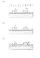
まず、本発明に係る半導体装置1について説明する。図1(a)は液晶表示装置の半導体装置1の要部平面図である。また、図1(b)は図1(a)におけるA−A線断面図であって、図1(c)は図1(a)におけるB−B線断面図である。Hereinafter, an embodiment embodying the present invention will be described with reference to the drawings.
First, the
図1(a)〜図1(c)に示すように、半導体装置1では、半導体基板2上に複数の電極3が形成されている。各電極3は、電気信号の入出力を行うための電極であり、電極パット3aと該電極パット3aに接続された配線3bとを含む。本実施形態では、複数の電極3が、半導体基板2の端縁近傍に所定のピッチで形成されており、各電極3の素材はアルミニウムである。 As shown in FIGS. 1A to 1C, in the
また、これら電極3は保護膜4によって被覆されている。各電極3の一部である電極パット3aは、それぞれ対応するように保護膜4に形成された開口部4aを通じて外部に露出されている。本実施形態においては、保護膜4は、酸化珪素による絶縁膜によって形成されている。 These
そして、図1(a)〜図1(c)に示すように、半導体基板2上に形成された保護膜4の上面には、凸部としての略半球状の複数の突起体5がそれぞれ電極3上に形成されている。突起体5の頂点部は、電極3の上面よりも高くなっている。これら突起体5は、電極3と略同じピッチで配置されている。本実施形態では、突起体5は感光性樹脂によって形成されている。該感光性樹脂にはアクリル樹脂を使用している。 As shown in FIGS. 1A to 1C, a plurality of substantially
さらに、図1(c)に示すように、保護膜4上には、突起体5及び電極3の組みをそれぞれ覆うように、複数の導電層6が形成されている。各導電層6は、対応する開口部4aを通じて、対応する電極3の電極パット3aに電気的に接続されている。このように、各突起体5と、対応する突起体5の上面全体を覆うように形成された導電層6とによって、突起電極8が構成される。本実施形態では、これら導電層6は金によって形成されており、突起体5の底面の寸法(R)と略等しくなるようにパターニングされている。以上のように半導体装置1は、電極3に電気的に接続された複数の突起電極8を半導体基板2上に有する。 Further, as shown in FIG. 1C, a plurality of
次に、本発明の半導体装置1の製造方法について、図2〜図4に従って説明する。図2〜図4は、本発明の半導体装置1の製造方法を順を追って示す断面図、即ち、図1(a)におけるB−B線断面図に対応する断面図である。 Next, a method for manufacturing the
先ず、図2(a)に示すように、半導体基板2上の所定の位置に電極3をアルミニウムにより形成する。さらに、電極3の電極パット3aを露出させる開口部4aを有する保護膜4で、電極3(配線3b)を被覆する。詳しくは、まず、電極3を含む半導体基板2上に酸化珪素層を成膜する。次に、スピンコート法、ディッピング法、スプレーコート法等により、酸化珪素層上に図示しないレジスト層を形成させる。そして、所定のパターンが形成されたマスクを用い、レジスト層に露光処理及び現像処理(フォトリソグラフィー処理)を施す。その後、このように所定の形状にパターニングしたレジストパターンをマスクとして、上記成膜した酸化珪素層のエッチングを行う。このエッチング処理によって、電極3の電極パット3aを露出させる開口部4aを有する保護膜4が形成される。そして、開口部4aが形成された後、前記したレジストパターンは剥離液等を用いて除去される。 First, as shown in FIG. 2A, an
次に、図2(b)に示すように、保護膜4上に突起体5を形成するための樹脂、即ち、ポジ型レジストとなる感光性樹脂としてのアクリル樹脂を塗布し、塗布したアクリル樹脂をプリベークすることによって樹脂層5aを形成する。本実施形態では、アクリル樹脂に添加される光硬化剤(紫外線硬化剤)は、光硬化(紫外線硬化)したアクリル樹脂が加温によって再び融解できる程度の添加量に調整されている。 Next, as shown in FIG. 2B, a resin for forming the
そして、図2(c)に示すように、樹脂層5a上に、マスク9を所定位置に位置決めして配置する。本実施形態では、マスク9は、例えば、クロム等の遮光膜を形成したガラス板からなり、形成すべき略半球状の突起体5の平面形状に対応した円形の開口部9aを有する。また、マスク9の位置決めは、マスク9の開口部9aが突起体5の形成箇所に位置するように行う。 And as shown in FIG.2 (c), the mask 9 is positioned and arrange | positioned on the resin layer 5a at a predetermined position. In the present embodiment, the mask 9 is made of, for example, a glass plate on which a light shielding film such as chromium is formed, and has a
次いで、図示しない紫外線ランプから、マスク9上に紫外線10を照射して、開口部9a内で露出されている樹脂層5aを露光させる。詳しくは、樹脂層5aの材質や厚さに応じて、標準的な露光量の紫外線10を照射して、開口部9a内で露出した樹脂層5aの部分を紫外線硬化させる。開口部9a内で露出した樹脂層5aの部分以外の未露光部分(紫外線硬化されなかった樹脂層5aの部分)は、現像処理により現像され、除去される。その結果、図2(d)に示すように、樹脂層5aから、上面が平面である円柱形状の突起体5bが得られる。 Next, ultraviolet rays 10 are irradiated onto the mask 9 from an ultraviolet lamp (not shown) to expose the resin layer 5a exposed in the
次に、図3(a)に示すように、図示しない赤外線ランプから、前記した突起体5bに赤外線11を照射して、突起体5bを加熱させる。詳しくは、紫外線硬化されたアクリル樹脂からなる突起体5bに対して赤外線11を照射することにより、該アクリル樹脂が融解するまで加熱する。この時、該アクリル樹脂は、添加された紫外線硬化剤の作用によって硬化されている一方、前述したように紫外線硬化剤の添加量が調整されたことにより高密度な架橋状態には至っていない。このため、突起体5bを形成するアクリル樹脂は、赤外線11によって加熱されて融解する。これにより、融解したアクリル樹脂に表面張力が生じるため、平面であった突起体5bの上面形状は、滑らかな曲面に変形する。その結果、円柱形状の突起体5bは、略半球形状の突起体5となる(図3(b)参照)。 Next, as shown in FIG. 3A, the
そして、図3(c)に示すように、保護膜4の開口部4aに露出する電極3の部分(電極パット3a)及び突起体5の上面を含む半導体基板2の表面全面に、スパッタ法によって、金属からなる導電材料を成膜することにより、導電材料層6aを形成する。本実施形態では、導電材料には金を使用しており、導電材料層6aは突起体5の底面の寸法Rと略等しくなるようにパターニングされている。 Then, as shown in FIG. 3C, the entire surface of the
次に、導電材料層6a上の全面にレジストをスピンコート法、ディッピング法、スプレーコート法等によって塗布し、レジスト膜を形成する。そして、導電材料層6aの平面形状(平面パターン)に対応したマスクを用いて、レジスト層に露光処理及び現像処理を施して、所定の形状にパターニングする。これにより、図4(a)に示すように、導電層6のパターン形状に対応したレジストパターン15が形成される。 Next, a resist is applied to the entire surface of the
さらに、レジストパターン15によって覆われない導電材料層6aの部分をエッチングにより除去する。これにより、図4(b)に示すように、開口部4aを含んで保護膜4上及び突起体5の上面全体を覆うようにして、電極3に電気的に接続される導電層6が形成される。そして、図4(c)に示すように、剥離液等を使用して、レジストパターン15を除去する。その結果、突起体5と、突起体5の上面全体を覆うようにして形成された導電層6と、によって突起電極8が形成される。以上により、紫外線10等の露光条件に左右されることなく略半球形状の突起体5が形成される半導体装置1を得ることができる。 Further, the portion of the
上記実施形態は以下の利点を有する。
(1)本実施形態では、アクリル樹脂を融解させることにより、突起体5を形成した。即ち、アクリル樹脂を融解させることで、その融解したアクリル樹脂に表面張力を生じさせ、断面が半円状となるような略半球形状の突起体5を形成した。従って、紫外線10の露光条件によって突起体5の形状制御が左右されることがないため、半導体装置1の生産性の向上を図ることができる。The above embodiment has the following advantages.
(1) In this embodiment, the
(2)本実施形態では、感光性樹脂としてのアクリル樹脂を使用して、突起体5を形成した。即ち、紫外線10を露光させることにより、アクリル樹脂を紫外線硬化させて、上面が平面である円柱形状の突起体5bを形成した。従って、突起体5bを融解させることにより、容易に、略半球形状の突起体5を形成することができる。 (2) In the present embodiment, the
(3)本実施形態によれば、アクリル樹脂を、赤外線11によって加熱し、融解させた。融解したアクリル樹脂には表面張力が生じるため、略半球形状の突起体5が形成される。従って、紫外線10の露光条件に左右されることなく突起体5が形成されるため、半導体装置1の生産性の向上を確実に図ることができる。 (3) According to this embodiment, the acrylic resin was heated and melted by the infrared rays 11. Since surface tension is generated in the melted acrylic resin, a substantially
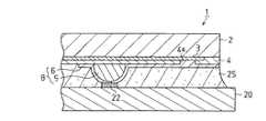
次に、前述した構成の半導体装置1を、実装基板としての配線基板20にCOG実装する方法及び実装構造を図5〜図7に従って説明する。
上記説明では、突起体5を、感光性絶縁樹脂としてのアクリル樹脂により形成した。感光性絶縁樹脂で突起体5を形成した場合は、導電樹脂で形成した場合に比べてコストを抑えて突起体5を形成することができる。Next, a method and a mounting structure for COG mounting the
In the above description, the
しかし、アクリル樹脂に限らず、フェノール樹脂、ポリイミド樹脂、又はエポキシ樹脂等で突起体5を形成してもよい。以下では、フェノール樹脂で突起体5を形成した場合について説明する。フェノール樹脂は、ガラス転移温度が300℃付近である第1の樹脂に相当する。 However, the
図5は、前述した半導体装置1を実装基板としての配線基板20にCOG実装した部分を拡大した断面図である。図5に示すように、配線基板20上には端子電極22が形成されており、端子電極22の上面には突起電極8が接続されている。端子電極22は、半導体装置1に形成された突起電極8の配置に対応して形成されている。詳しくは、半導体装置1の突起電極8を配線基板20の端子電極22に接続する方法として、NCP(N on Conductive Paste)方式を採用している。従って、NCPとしての接合材25を間に挟んで、半導体装置1が配線基板20に実装されることにより、突起電極8と端子電極22は、互いに電気的に接続された状態のまま固定される。 FIG. 5 is an enlarged cross-sectional view of a portion where the above-described
次に、半導体装置1を配線基板20に実装する方法について、図6(a)〜図6(b)に従って説明する。
図6(a)に示すように、配線基板20上には、配線基板20に半導体装置1を実装するための接合材25が塗布される。この例では、接合材25には、硬化温度が270℃付近であるエポキシ樹脂を使用している。図6(b)に示すように、半導体装置1の突起電極8を配線基板20の端子電極22に対して位置合わせを行い、フリップチップボンダによって半導体基板2と配線基板20とを加熱加圧する。これにより、半導体装置1は接合材25を間に挟んで、図5に示すように、配線基板20に実装される。Next, a method for mounting the
As shown in FIG. 6A, a
図7は、実装温度が210℃又は270℃の場合であって、加圧条件を5kgf/cm2(0.49MPa)又は10kgf/cm2(0.98MPa)として半導体基板2と配線基板20とを加熱加圧した場合に、突起電極8に含まれる導電層6の断線の有無を表した図である。この例では、突起体5を構成する樹脂として、ガラス転移温度が220℃付近であるアクリル樹脂と、ガラス転移温度が300℃付近であるフェノール樹脂とを、前記した実装温度及び加圧条件に対してそれぞれ使用した。FIG. 7 shows a case where the mounting temperature is 210 ° C. or 270 ° C., and the
突起体5を形成する樹脂に、ガラス転移温度が220℃の樹脂(アクリル樹脂)を使用した場合、実装温度が210℃でも、ガラス転移温度付近となって弾性率の低下が開始する。よって、実装温度が270℃の場合のみならず、実装温度が210℃の場合でも、10kgf/cm2で半導体装置1を加圧した場合、突起体5の樹脂が大きく変形してしまう。その結果、突起電極8に含まれる導電層6は、突起体5の大きな変形に追随できずに断線してしまう。よって、半導体装置1を、5kgf/cm2の低荷重で配線基板20に実装しなければならない。When a resin (acrylic resin) having a glass transition temperature of 220 ° C. is used as the resin for forming the
一方、突起体5を形成する樹脂に、ガラス転移温度が270℃以上の樹脂(フェノール樹脂)を使用した場合、同じ実装条件となるように実装温度が210℃や270℃の場合であっても、突起体5の弾性率は高いまま維持される。よって、突起体5の樹脂の変形は大きくなく、導電層6の断線は発生しない。On the otherhand, the resin forming the
詳しくは、実装温度を270℃に設定し、突起電極8を端子電極22に対して位置合わせを行って、フリップチップボンダにより半導体基板2と配線基板20とを加熱加圧する。このとき、突起体5を形成するフェノール樹脂は、ガラス転移温度が300℃付近であるため、フェノール樹脂の弾性率は低下せずに、高い弾性率の状態を維持している。従って、フリップチップボンダによる加圧に対して、NCPとしての接合材25が硬化する時、即ち、実装温度が270℃となった時でも、フェノール樹脂からなる突起体5は必要以上に大きくは変形しない。つまり、略半球状に形成された突起体5の頂点部付近に加圧による負荷が集中的にかかるため、頂点部付近のフェノール樹脂だけが変形する。このため、導電層6が断線することはなく、半導体装置1の突起電極8と配線基板20の端子電極22との間の電気的な接続が確保される。従って、実装温度が210℃と270℃のいずれであっても、また、加圧条件が5kgf/cm2及び10kgf/cm2のいずれの場合であっても、突起体5を形成するフェノール樹脂の弾性率は高い状態のまま維持されることになり、突起体5は大きく変形することがない。即ち、突起電極8の形状が大きく変化することはないため、突起電極8を構成する導電層6は断線しない。Specifically, the mounting temperature is set to 270 ° C., the protruding
エポキシ樹脂から構成される接合材25を硬化させることにより、前述した突起電極8と端子電極22との間の接続状態を固定、保持させる。以上の工程により、半導体装置1の突起電極8と配線基板20の端子電極22との間の接続信頼性を保持しながら、半導体装置1を配線基板20に実装することができる。 By curing the
上記半導体装置の実装方法は、以下の利点を有する。
(11)接合材25の硬化温度よりもガラス転移温度の高い樹脂を使用して突起体5を形成した。つまり、接合材25を構成する樹脂には硬化温度が250℃であるエポキシ樹脂を使用し、突起体5を形成する樹脂にはガラス転移温度が300℃付近であるフェノール樹脂を使用した。Mounting method of the semiconductor devicehas the advantage offollowing.
(11) The
これにより、半導体装置1の実装時の設定温度を、突起体5を形成するフェノール樹脂のガラス転移温度(300℃付近)以下である270℃にすることができる。即ち、実装温度を270℃とすることで、実装時において突起体5の弾性率を高い弾性率に維持したまま、半導体装置1を配線基板20に実装できる。従って、実装時に突起体5が必要以上に大きく変形することがなく、突起電極8に含まれる導電層6の断線を抑制することができる。このため、半導体装置1の突起電極8と配線基板20の端子電極22との間の接続信頼性の向上を図ることができる。 Thereby, the setting temperature at the time of mounting of the
(12)突起体5は略半球状の形状をしている。これにより、半導体装置1の実装時の加熱加圧によって、突起体5の頂点部付近に圧力が集中的にかかる。つまり、突起体5を構成する樹脂全体は、半導体装置1の実装時に高い弾性率を維持していても、突起体5の頂点部付近に集中して荷重がかかることになり、突起体5の頂点部付近の樹脂だけを変形させることができる。従って、突起電極8と端子電極22との接触面積を増加させることができるため、より確実に、半導体装置1の突起電極8と配線基板20の端子電極22との間の接続信頼性の向上を図ることができる。(12)
(13)突起体5を形成する樹脂にフェノール樹脂を使用した。フェノール樹脂のガラス転移温度は300℃付近であるため、硬化温度が270℃付近であるエポキシ樹脂によって構成される接合材25が硬化する温度であっても、突起体5を形成するフェノール樹脂は高い弾性率を維持することができる。即ち、実装時に突起体5が必要以上に大きく変形することを防止でき、突起電極8を構成する導電層6が断線することを抑制することができる。従って、半導体装置1の突起電極8と配線基板20の端子電極22との間の接続信頼性の向上を図ることができる。(13) was used a phenolic resin in the resin forming the
(14)接合材25は、エポキシ樹脂から構成されるNCP(Non Conductive Paste)である。これにより、導電微粒子を含んだ接合材25を使用することなく、低コストな非導電性接合材としての接合材25を使用して、半導体装置1を配線基板20に確実に実装することができる。従って、生産性を低下させることなく、半導体装置1の突起電極8と配線基板20の端子電極22とを電気的に接続することができ、接続信頼性の向上を図ることができる。(14)
なお、本実施形態や上記実装方法は以下のように変更してもよい。
○図5〜図7では、突起体5を形成する樹脂には、ガラス転移温度が300℃であるフェノール樹脂を使用した。しかし、突起体5を形成する樹脂としては、ガラス転移温度が270℃以上である樹脂を使用するのであれば他の樹脂を使用してもよい。この場合でも、接合材25には、硬化温度が250℃以上である生産性のよい接合材25を使用することができる。従って、生産性を低下させることなく、半導体装置1の突起電極8と配線基板20上の端子電極22との間の接続信頼性の向上を図ることができる。In addition, you may change this embodimentand the said mounting method as follows.
In FIG. 5 to FIG. 7, a phenol resin having a glass transition temperature of 300 ° C. was used as the resin forming the
○図5〜図7では、突起体5を形成する樹脂にはフェノール樹脂を使用した。これに代えて、突起体5を形成する樹脂として、ガラス転移温度の高いポリイミド樹脂等を使用してもよい。これにより、突起体5を形成する樹脂は、実装時でも高い弾性率を維持することができる。即ち、実装時に突起体5が必要以上に大きく変形することを防止でき、導電層6が断線するのを抑制することができる。従って、半導体装置1の突起電極8と配線基板20上の端子電極22との間の接続信頼性の向上を図ることができる。In FIGS. 5 to 7, phenol resin is used as the resin for forming the
○上記実施形態では、マスク9の開口部9aの形状を、略半球状の突起体5の平面形状に対応した円形とした。これに代えて、開口部9aの形状は特に限定する必要はなく、例えば、四角形であってもよい。その結果、紫外線10の露光処理によって、直方体状の突起体5bが形成される。この場合でも、突起体5bを融解させることにより、表面張力によって、半円状の断面形状を有する突起体5を形成することができる。 In the above embodiment, the shape of the
○上記実施形態では、マスク9に紫外線10を照射することにより、開口部9a内で露出されている樹脂層5aの部分を紫外線架橋させて突起体5bを形成した。これに代えて、マスク9上に電子線を照射することにより、開口部9a内で露出されている樹脂層5aの部分を電子線架橋させて突起体5bを形成してもよい。 In the above embodiment, the
○上記実施形態では、赤外線11によって突起体5bを融解させて略半球形状の突起体5を形成した。これに代えて、レーザ光等の他の手段に基づく放射熱によって突起体5bを加熱してもよい。特にレーザ光は局部的に加熱を行うことができるため、容易に突起体5bを加熱して融解させることができる。従って、より一段と半導体装置1の生産性の向上を図ることができる。 In the above embodiment, the
○上記実施形態では、半導体基板2上に形成される各々の電極3に対応させて突起体5を形成した。これに代えて、図8に示すように、複数の電極3を跨るように突起体5を形成して、該突起体5の上面に各々の電極3に対応した導電層6を形成し、組となる電極3と導電層6とを互いに電気的に接続させてもよい。これにより、複数の電極3それぞれに突起体5を形成する必要がなく、より一段と半導体装置1の製造時間の短縮化すなわち生産性の向上を図ることができる。更に、半導体装置1の突起電極8と配線基板20上の端子電極22との間の接続信頼性の向上を図ることができる。 In the above embodiment, the
○上記実施形態では、保護膜4は酸化珪素により形成した。これに代えて、保護膜4は、窒化珪素、ポリイミド樹脂等によって形成してもよい。
○上記実施形態では、保護膜4の膜厚を限定しなかったが、例えば1μm程度に形成すればよい。In the above embodiment, the
In the above embodiment, the thickness of the
○上記実施形態では、導電層6は矩形形状にパターニングして形成した。これに代えて、導電層6の形状は特に限定する必要はなく、例えば、正方形形状にパターニングして形成してもよい。 In the above embodiment, the
○上記実施形態では、導電層6は金によって形成した。これに代えて、導電層6の素材には、例えば、銅、ニッケル、チタン、アルミニウム等、他の金属を使用してもよい。 In the above embodiment, the
1…半導体装置、2…半導体基板、3…電極、4…保護膜、5…凸部としての突起体、6…導電層、8…突起電極、9…マスク、10…紫外線、11…赤外線、20…実装基板としての配線基板、22…端子電極、25…接合材。DESCRIPTION OF
Claims (5)
Translated fromJapaneseこの形成した電極の一部が露出される態様にて電極及び半導体基板を絶縁性の保護膜で被覆することと、
この被覆した保護膜を含む全面に感光性樹脂からなる樹脂層を形成することと、
この形成した樹脂層に対するマスクを介した選択的な露光を通じて同樹脂による柱状の突起体を形成するとともに、それ以外の樹脂層を現像除去することと、
この形成された柱状の突起体を放射熱の加熱によって融解させて断面が半円状となる凸部を形成することと、
前記電極の露出された一部及びこの断面が半円状となる凸部を含む全面に導電性材料を成膜した後これをパターニングすることにより前記電極に電気的に接続されて前記凸部の上面に至る導電層を形成することと、
を含む半導体装置の製造方法。Forming an electrode on a semiconductor substrate;
Covering the electrode and the semiconductor substrate with an insulating protective film in a manner in which a part of the formed electrode is exposed;
Forming a resin layer made of a photosensitive resin on the entire surface including the coated protective film;
Forming the columnar protrusions of the resin through selective exposure through a mask to the formed resin layer, and developing and removing the other resin layers;
Melting the formed columnar protrusions by heating with radiant heat to form a convex portion having a semicircular cross section;
A conductive material is formed on the entire surface including the exposed part of the electrode and the convex part having a semicircular cross section, and is then electrically connected to the electrode by patterning the conductive material. Forming a conductive layer reaching the top surface;
A method of manufacturinga semiconductor deviceincluding :
前記感光性樹脂からなる樹脂層として、光硬化した樹脂が加温によって再び融解できる量の光硬化剤が添加されたものを用いることを特徴とする半導体装置の製造方法。 A method for manufacturing a semiconductor device, wherein a resin layer made of a photosensitive resin to which a photocuring agent is added in such an amount that the photocured resin can be melted again by heating is used.
前記感光性樹脂からなる樹脂層としてアクリル樹脂を用いることを特徴とする半導体装置の製造方法。 A method of manufacturing a semiconductor device, wherein an acrylic resin is used as the resin layer made of the photosensitive resin.
前記感光性樹脂からなる樹脂層としてフェノール樹脂又はポリイミド樹脂又はエポキシ樹脂を用いることを特徴とする半導体装置の製造方法。 A method for manufacturing a semiconductor device, wherein a phenol resin, a polyimide resin, or an epoxy resin is used as the resin layer made of the photosensitive resin.
前記電極を複数設け、互いに隣接する前記複数の電極を跨るように前記凸部を形成し、前記凸部の上面に前記電極の各々に対応して前記導電層を形成し、前記導電層の各々と、対応する前記電極とを電気的に接続することを特徴とする半導体装置の製造方法。 Providing a plurality of the electrodes, forming the convex portion so as to straddle the plurality of adjacent electrodes, forming the conductive layer corresponding to each of the electrodes on the upper surface of the convex portion, each of the conductive layers And a corresponding electrode are electrically connected to each other.
Priority Applications (10)
| Application Number | Priority Date | Filing Date | Title |
|---|---|---|---|
| JP2005344647AJP4142041B2 (en) | 2005-03-23 | 2005-11-29 | Manufacturing method of semiconductor device |
| TW097132409ATWI450315B (en) | 2005-03-23 | 2006-03-10 | Method for implementing semiconductor device |
| TW095108154ATWI336097B (en) | 2005-03-23 | 2006-03-10 | Method for manufacturing semiconductor device |
| CN 200910142031CN101562143B (en) | 2005-03-23 | 2006-03-21 | Manufacturing method of semiconductor device, mounting method and mounting structure of semiconductor device |
| CN 200610068103CN100595890C (en) | 2005-03-23 | 2006-03-21 | Method for fabricating semiconductor device |
| CN 200910142033CN101562144B (en) | 2005-03-23 | 2006-03-21 | Method for manufacturing a semiconductor device, method and structure for mounting the semiconductor device |
| US11/386,019US7524700B2 (en) | 2005-03-23 | 2006-03-21 | Method for manufacturing semiconductor device, and method and structure for implementing semicondutor device |
| KR1020060026054AKR100730848B1 (en) | 2005-03-23 | 2006-03-22 | Method for manufacturing semiconductor device, and method and structure for implementing semiconductor device |
| US12/102,416US7601626B2 (en) | 2005-03-23 | 2008-04-14 | Method for manufacturing semiconductor device, and method and structure for implementing semiconductor device |
| US12/552,728US8207056B2 (en) | 2005-03-23 | 2009-09-02 | Method for manufacturing semiconductor device, and method and structure for implementing semiconductor device |
Applications Claiming Priority (3)
| Application Number | Priority Date | Filing Date | Title |
|---|---|---|---|
| JP2005084583 | 2005-03-23 | ||
| JP2005084584 | 2005-03-23 | ||
| JP2005344647AJP4142041B2 (en) | 2005-03-23 | 2005-11-29 | Manufacturing method of semiconductor device |
Related Child Applications (1)
| Application Number | Title | Priority Date | Filing Date |
|---|---|---|---|
| JP2008019727ADivisionJP2008124501A (en) | 2005-03-23 | 2008-01-30 | Mounting method and mounting structure of semiconductor device |
Publications (2)
| Publication Number | Publication Date |
|---|---|
| JP2006303420A JP2006303420A (en) | 2006-11-02 |
| JP4142041B2true JP4142041B2 (en) | 2008-08-27 |
Family
ID=37035768
Family Applications (1)
| Application Number | Title | Priority Date | Filing Date |
|---|---|---|---|
| JP2005344647AExpired - Fee RelatedJP4142041B2 (en) | 2005-03-23 | 2005-11-29 | Manufacturing method of semiconductor device |
Country Status (4)
| Country | Link |
|---|---|
| US (3) | US7524700B2 (en) |
| JP (1) | JP4142041B2 (en) |
| KR (1) | KR100730848B1 (en) |
| TW (2) | TWI336097B (en) |
Families Citing this family (11)
| Publication number | Priority date | Publication date | Assignee | Title |
|---|---|---|---|---|
| JP4572376B2 (en)* | 2007-07-30 | 2010-11-04 | セイコーエプソン株式会社 | Semiconductor device manufacturing method and electronic device manufacturing method |
| JP5077540B2 (en)* | 2007-08-10 | 2012-11-21 | セイコーエプソン株式会社 | Manufacturing method of semiconductor device |
| JP5088488B2 (en)* | 2008-03-03 | 2012-12-05 | セイコーエプソン株式会社 | Semiconductor module and manufacturing method thereof |
| JP4936010B2 (en)* | 2008-03-03 | 2012-05-23 | セイコーエプソン株式会社 | Semiconductor module and manufacturing method thereof |
| JP4737466B2 (en) | 2009-02-09 | 2011-08-03 | セイコーエプソン株式会社 | Semiconductor device and manufacturing method thereof |
| CN102299121A (en)* | 2011-05-20 | 2011-12-28 | 电子科技大学 | Method for packaging photoelectronic device |
| CN102299120A (en)* | 2011-05-20 | 2011-12-28 | 电子科技大学 | Packaging method of optoelectronic device |
| CN102299119A (en)* | 2011-05-20 | 2011-12-28 | 电子科技大学 | Method for packaging photoelectronic device |
| CN102299118A (en)* | 2011-05-20 | 2011-12-28 | 电子科技大学 | Method for packaging photoelectronic device |
| CN102299122A (en)* | 2011-05-20 | 2011-12-28 | 电子科技大学 | Method for packaging photoelectronic device |
| US11316086B2 (en)* | 2020-07-10 | 2022-04-26 | X Display Company Technology Limited | Printed structures with electrical contact having reflowable polymer core |
Family Cites Families (31)
| Publication number | Priority date | Publication date | Assignee | Title |
|---|---|---|---|---|
| US4813129A (en) | 1987-06-19 | 1989-03-21 | Hewlett-Packard Company | Interconnect structure for PC boards and integrated circuits |
| JPH0621257Y2 (en) | 1987-07-16 | 1994-06-01 | 三洋電機株式会社 | Solid-state imaging device |
| FR2676920B1 (en)* | 1991-05-31 | 1998-11-20 | Vanraes Pierre | SLEEVE WITH EACH HALF A HALF HOLLOWED TO CLEAN THE HEARING DUCTS, EITHER AN EAR CURE, FLEXIBLE PLASTIC MATERIAL. |
| JP2833326B2 (en)* | 1992-03-03 | 1998-12-09 | 松下電器産業株式会社 | Electronic component mounted connector and method of manufacturing the same |
| US5359768A (en)* | 1992-07-30 | 1994-11-01 | Intel Corporation | Method for mounting very small integrated circuit package on PCB |
| JP3297144B2 (en)* | 1993-05-11 | 2002-07-02 | シチズン時計株式会社 | Protrusion electrode and method of manufacturing the same |
| US5508228A (en) | 1994-02-14 | 1996-04-16 | Microelectronics And Computer Technology Corporation | Compliant electrically connective bumps for an adhesive flip chip integrated circuit device and methods for forming same |
| JPH07263493A (en) | 1994-03-18 | 1995-10-13 | World Metal:Kk | Chip mounting method |
| JPH1027824A (en) | 1996-02-23 | 1998-01-27 | Matsushita Electric Ind Co Ltd | Semiconductor device having protruding electrode and method of manufacturing the same |
| DE69830883T2 (en)* | 1997-03-10 | 2006-04-20 | Seiko Epson Corp. | Semiconductor device and equipped with this device circuit board |
| JP3632882B2 (en) | 1997-06-27 | 2005-03-23 | ソニー株式会社 | Semiconductor device and manufacturing method thereof |
| CA2325886C (en)* | 1998-04-09 | 2009-07-21 | California Institute Of Technology | Electronic techniques for analyte detection |
| US6277669B1 (en)* | 1999-09-15 | 2001-08-21 | Industrial Technology Research Institute | Wafer level packaging method and packages formed |
| JP2001110831A (en) | 1999-10-07 | 2001-04-20 | Seiko Epson Corp | External connection projection and method of forming the same, semiconductor chip, circuit board, and electronic device |
| US6770547B1 (en)* | 1999-10-29 | 2004-08-03 | Renesas Technology Corporation | Method for producing a semiconductor device |
| TW498468B (en)* | 1999-10-29 | 2002-08-11 | Hitachi Ltd | Semiconductor device |
| US6710446B2 (en)* | 1999-12-30 | 2004-03-23 | Renesas Technology Corporation | Semiconductor device comprising stress relaxation layers and method for manufacturing the same |
| JP2002162652A (en) | 2000-01-31 | 2002-06-07 | Fujitsu Ltd | Sheet display device, resin spherical body, and microcapsule |
| MY131961A (en)* | 2000-03-06 | 2007-09-28 | Hitachi Chemical Co Ltd | Resin composition, heat-resistant resin paste and semiconductor device using them and method for manufacture thereof |
| DE10014300A1 (en)* | 2000-03-23 | 2001-10-04 | Infineon Technologies Ag | Semiconductor component and method for its production |
| DE10016132A1 (en)* | 2000-03-31 | 2001-10-18 | Infineon Technologies Ag | Electronic component with flexible contact points and method for its production |
| JP4174174B2 (en)* | 2000-09-19 | 2008-10-29 | 株式会社ルネサステクノロジ | Semiconductor device, manufacturing method thereof, and semiconductor device mounting structure |
| JP3642414B2 (en)* | 2001-02-08 | 2005-04-27 | シャープ株式会社 | Semiconductor device and manufacturing method thereof |
| JP2003124244A (en) | 2001-10-11 | 2003-04-25 | Fujikura Ltd | Method for manufacturing semiconductor device |
| TW517360B (en)* | 2001-12-19 | 2003-01-11 | Ind Tech Res Inst | Enhanced type wafer level package structure and its manufacture method |
| JP3969295B2 (en) | 2002-12-02 | 2007-09-05 | セイコーエプソン株式会社 | SEMICONDUCTOR DEVICE, ITS MANUFACTURING METHOD, CIRCUIT BOARD, ELECTRO-OPTICAL DEVICE, AND ELECTRONIC DEVICE |
| JP3906921B2 (en) | 2003-06-13 | 2007-04-18 | セイコーエプソン株式会社 | Bump structure and manufacturing method thereof |
| JP2005101527A (en) | 2003-08-21 | 2005-04-14 | Seiko Epson Corp | Electronic component mounting structure, electro-optical device, electronic apparatus, and electronic component mounting method |
| JP4218622B2 (en) | 2003-10-09 | 2009-02-04 | セイコーエプソン株式会社 | Manufacturing method of semiconductor device |
| JP4281656B2 (en)* | 2004-09-22 | 2009-06-17 | セイコーエプソン株式会社 | Electronic component mounting structure, electronic component mounting method, electro-optical device, and electronic apparatus |
| JP4061506B2 (en)* | 2005-06-21 | 2008-03-19 | セイコーエプソン株式会社 | Manufacturing method of semiconductor device |
- 2005
- 2005-11-29JPJP2005344647Apatent/JP4142041B2/ennot_activeExpired - Fee Related
- 2006
- 2006-03-10TWTW095108154Apatent/TWI336097B/ennot_activeIP Right Cessation
- 2006-03-10TWTW097132409Apatent/TWI450315B/ennot_activeIP Right Cessation
- 2006-03-21USUS11/386,019patent/US7524700B2/ennot_activeExpired - Fee Related
- 2006-03-22KRKR1020060026054Apatent/KR100730848B1/ennot_activeExpired - Fee Related
- 2008
- 2008-04-14USUS12/102,416patent/US7601626B2/ennot_activeExpired - Fee Related
- 2009
- 2009-09-02USUS12/552,728patent/US8207056B2/ennot_activeExpired - Fee Related
Also Published As
| Publication number | Publication date |
|---|---|
| TW200705537A (en) | 2007-02-01 |
| US7601626B2 (en) | 2009-10-13 |
| KR20060103138A (en) | 2006-09-28 |
| KR100730848B1 (en) | 2007-06-20 |
| TW200903577A (en) | 2009-01-16 |
| US7524700B2 (en) | 2009-04-28 |
| US8207056B2 (en) | 2012-06-26 |
| TWI450315B (en) | 2014-08-21 |
| US20080206980A1 (en) | 2008-08-28 |
| TWI336097B (en) | 2011-01-11 |
| JP2006303420A (en) | 2006-11-02 |
| US20090317969A1 (en) | 2009-12-24 |
| US20060216919A1 (en) | 2006-09-28 |
Similar Documents
| Publication | Publication Date | Title |
|---|---|---|
| KR100730848B1 (en) | Method for manufacturing semiconductor device, and method and structure for implementing semiconductor device | |
| KR100643984B1 (en) | Method for mounting semiconductor device, circuit board, electrooptic device, and electronic device | |
| US7002250B2 (en) | Semiconductor module | |
| JP4840373B2 (en) | Semiconductor device and manufacturing method thereof | |
| JP4784304B2 (en) | Electronic component, method for manufacturing electronic component, circuit board, and electronic device | |
| US8330256B2 (en) | Semiconductor device having through electrodes, a manufacturing method thereof, and an electronic apparatus | |
| JP2002261190A (en) | Semiconductor device, method for manufacturing the same and electronic equipment | |
| JP4729963B2 (en) | PROJECT ELECTRODE FOR CONNECTING ELECTRONIC COMPONENT, ELECTRONIC COMPONENT MOUNTING BODY USING SAME, AND METHOD FOR PRODUCING THEM | |
| JP2007250618A (en) | Electronic component mounting structure and manufacturing method thereof | |
| CN100595890C (en) | Method for fabricating semiconductor device | |
| JP4151634B2 (en) | SEMICONDUCTOR DEVICE AND ITS MANUFACTURING METHOD, CIRCUIT BOARD, ELECTRO-OPTICAL DEVICE, AND ELECTRONIC DEVICE | |
| JP7357243B2 (en) | Semiconductor device, mounting structure of semiconductor device, and manufacturing method of semiconductor device | |
| JP4453533B2 (en) | Protruding electrode for connecting electronic parts and method for manufacturing the same | |
| JP2008124501A (en) | Mounting method and mounting structure of semiconductor device | |
| JP2001244366A (en) | Semiconductor integrated circuit device and method of manufacturing the same | |
| JP2005129756A (en) | Semiconductor element bonding method | |
| JP2012079956A (en) | Semiconductor device and method for manufacturing the same | |
| JPH07176565A (en) | Wiring board and manufacturing method thereof | |
| CN101964308B (en) | Method for manufacturing semiconductor device, semiconductor device, and semiconductor manufacturing equipment | |
| JP2980402B2 (en) | Manufacturing method of intermediate board for mounting circuit parts | |
| JP2006310532A (en) | Semiconductor device and manufacturing method thereof | |
| JP2002299361A (en) | Semiconductor device and its manufacturing method, circuit board, and electronic equipment | |
| JPWO2002078079A1 (en) | Semiconductor device package and method of manufacturing the same | |
| JPH06326154A (en) | Multichip module board |
Legal Events
| Date | Code | Title | Description |
|---|---|---|---|
| A977 | Report on retrieval | Free format text:JAPANESE INTERMEDIATE CODE: A971007 Effective date:20071121 | |
| A131 | Notification of reasons for refusal | Free format text:JAPANESE INTERMEDIATE CODE: A131 Effective date:20071204 | |
| A521 | Written amendment | Free format text:JAPANESE INTERMEDIATE CODE: A523 Effective date:20080130 | |
| TRDD | Decision of grant or rejection written | ||
| A01 | Written decision to grant a patent or to grant a registration (utility model) | Free format text:JAPANESE INTERMEDIATE CODE: A01 Effective date:20080513 | |
| A01 | Written decision to grant a patent or to grant a registration (utility model) | Free format text:JAPANESE INTERMEDIATE CODE: A01 | |
| A61 | First payment of annual fees (during grant procedure) | Free format text:JAPANESE INTERMEDIATE CODE: A61 Effective date:20080611 | |
| FPAY | Renewal fee payment (event date is renewal date of database) | Free format text:PAYMENT UNTIL: 20110620 Year of fee payment:3 | |
| R150 | Certificate of patent or registration of utility model | Ref document number:4142041 Country of ref document:JP Free format text:JAPANESE INTERMEDIATE CODE: R150 Free format text:JAPANESE INTERMEDIATE CODE: R150 | |
| FPAY | Renewal fee payment (event date is renewal date of database) | Free format text:PAYMENT UNTIL: 20110620 Year of fee payment:3 | |
| FPAY | Renewal fee payment (event date is renewal date of database) | Free format text:PAYMENT UNTIL: 20120620 Year of fee payment:4 | |
| FPAY | Renewal fee payment (event date is renewal date of database) | Free format text:PAYMENT UNTIL: 20130620 Year of fee payment:5 | |
| FPAY | Renewal fee payment (event date is renewal date of database) | Free format text:PAYMENT UNTIL: 20130620 Year of fee payment:5 | |
| S531 | Written request for registration of change of domicile | Free format text:JAPANESE INTERMEDIATE CODE: R313531 | |
| R350 | Written notification of registration of transfer | Free format text:JAPANESE INTERMEDIATE CODE: R350 | |
| R250 | Receipt of annual fees | Free format text:JAPANESE INTERMEDIATE CODE: R250 | |
| LAPS | Cancellation because of no payment of annual fees |