JP4135448B2 - Method for manufacturing droplet ejecting apparatus - Google Patents
Method for manufacturing droplet ejecting apparatusDownload PDFInfo
- Publication number
- JP4135448B2 JP4135448B2JP2002269862AJP2002269862AJP4135448B2JP 4135448 B2JP4135448 B2JP 4135448B2JP 2002269862 AJP2002269862 AJP 2002269862AJP 2002269862 AJP2002269862 AJP 2002269862AJP 4135448 B2JP4135448 B2JP 4135448B2
- Authority
- JP
- Japan
- Prior art keywords
- electrode
- plate
- forming
- liquid storage
- liquid
- Prior art date
- Legal status (The legal status is an assumption and is not a legal conclusion. Google has not performed a legal analysis and makes no representation as to the accuracy of the status listed.)
- Expired - Fee Related
Links
- 238000004519manufacturing processMethods0.000titleclaimsdescription35
- 238000000034methodMethods0.000titleclaimsdescription30
- 239000007788liquidSubstances0.000claimsdescription94
- 238000003860storageMethods0.000claimsdescription49
- 230000005684electric fieldEffects0.000claimsdescription31
- 230000007246mechanismEffects0.000claimsdescription22
- 238000005192partitionMethods0.000claimsdescription17
- 230000015556catabolic processEffects0.000claimsdescription15
- 239000002131composite materialSubstances0.000claimsdescription14
- 238000005304joiningMethods0.000claimsdescription12
- 230000008569processEffects0.000claimsdescription9
- 230000015572biosynthetic processEffects0.000claimsdescription7
- 238000003825pressingMethods0.000claimsdescription7
- 239000000463materialSubstances0.000claimsdescription6
- 230000010287polarizationEffects0.000claimsdescription6
- 230000001678irradiating effectEffects0.000claimsdescription4
- 238000003475laminationMethods0.000claims2
- 239000000919ceramicSubstances0.000description82
- 238000004891communicationMethods0.000description13
- 238000006073displacement reactionMethods0.000description13
- 229910003460diamondInorganic materials0.000description8
- 239000010432diamondSubstances0.000description8
- 230000000694effectsEffects0.000description8
- 238000004140cleaningMethods0.000description7
- 238000003754machiningMethods0.000description7
- 239000000853adhesiveSubstances0.000description4
- 230000001070adhesive effectEffects0.000description4
- 230000008901benefitEffects0.000description4
- 238000010586diagramMethods0.000description4
- 238000010030laminatingMethods0.000description4
- 229910052451lead zirconate titanateInorganic materials0.000description4
- 125000006850spacer groupChemical group0.000description4
- 230000008859changeEffects0.000description3
- 230000004048modificationEffects0.000description3
- 238000012986modificationMethods0.000description3
- 238000007639printingMethods0.000description3
- 230000009467reductionEffects0.000description3
- 238000009751slip formingMethods0.000description3
- 229920001187thermosetting polymerPolymers0.000description3
- 239000004593EpoxySubstances0.000description2
- 239000004642PolyimideSubstances0.000description2
- 229910010293ceramic materialInorganic materials0.000description2
- 238000010304firingMethods0.000description2
- HFGPZNIAWCZYJU-UHFFFAOYSA-Nlead zirconate titanateChemical compound[O-2].[O-2].[O-2].[O-2].[O-2].[Ti+4].[Zr+4].[Pb+2]HFGPZNIAWCZYJU-UHFFFAOYSA-N0.000description2
- 239000007769metal materialSubstances0.000description2
- 229920001721polyimidePolymers0.000description2
- 229920003002synthetic resinPolymers0.000description2
- 239000000057synthetic resinSubstances0.000description2
- 238000006243chemical reactionMethods0.000description1
- 230000006378damageEffects0.000description1
- 239000000428dustSubstances0.000description1
- 238000005401electroluminescenceMethods0.000description1
- 238000005530etchingMethods0.000description1
- 239000012530fluidSubstances0.000description1
- 238000002347injectionMethods0.000description1
- 239000007924injectionSubstances0.000description1
- 229910000679solderInorganic materials0.000description1
Images


Classifications
- B—PERFORMING OPERATIONS; TRANSPORTING
- B41—PRINTING; LINING MACHINES; TYPEWRITERS; STAMPS
- B41J—TYPEWRITERS; SELECTIVE PRINTING MECHANISMS, i.e. MECHANISMS PRINTING OTHERWISE THAN FROM A FORME; CORRECTION OF TYPOGRAPHICAL ERRORS
- B41J2/00—Typewriters or selective printing mechanisms characterised by the printing or marking process for which they are designed
- B41J2/005—Typewriters or selective printing mechanisms characterised by the printing or marking process for which they are designed characterised by bringing liquid or particles selectively into contact with a printing material
- B41J2/01—Ink jet
- B41J2/135—Nozzles
- B41J2/16—Production of nozzles
- B41J2/1621—Manufacturing processes
- B41J2/1623—Manufacturing processes bonding and adhesion
- B—PERFORMING OPERATIONS; TRANSPORTING
- B41—PRINTING; LINING MACHINES; TYPEWRITERS; STAMPS
- B41J—TYPEWRITERS; SELECTIVE PRINTING MECHANISMS, i.e. MECHANISMS PRINTING OTHERWISE THAN FROM A FORME; CORRECTION OF TYPOGRAPHICAL ERRORS
- B41J2/00—Typewriters or selective printing mechanisms characterised by the printing or marking process for which they are designed
- B41J2/005—Typewriters or selective printing mechanisms characterised by the printing or marking process for which they are designed characterised by bringing liquid or particles selectively into contact with a printing material
- B41J2/01—Ink jet
- B41J2/135—Nozzles
- B41J2/14—Structure thereof only for on-demand ink jet heads
- B41J2/14201—Structure of print heads with piezoelectric elements
- B41J2/14209—Structure of print heads with piezoelectric elements of finger type, chamber walls consisting integrally of piezoelectric material
- B—PERFORMING OPERATIONS; TRANSPORTING
- B41—PRINTING; LINING MACHINES; TYPEWRITERS; STAMPS
- B41J—TYPEWRITERS; SELECTIVE PRINTING MECHANISMS, i.e. MECHANISMS PRINTING OTHERWISE THAN FROM A FORME; CORRECTION OF TYPOGRAPHICAL ERRORS
- B41J2/00—Typewriters or selective printing mechanisms characterised by the printing or marking process for which they are designed
- B41J2/005—Typewriters or selective printing mechanisms characterised by the printing or marking process for which they are designed characterised by bringing liquid or particles selectively into contact with a printing material
- B41J2/01—Ink jet
- B41J2/135—Nozzles
- B41J2/16—Production of nozzles
- B41J2/1607—Production of print heads with piezoelectric elements
- B41J2/1609—Production of print heads with piezoelectric elements of finger type, chamber walls consisting integrally of piezoelectric material
- B—PERFORMING OPERATIONS; TRANSPORTING
- B41—PRINTING; LINING MACHINES; TYPEWRITERS; STAMPS
- B41J—TYPEWRITERS; SELECTIVE PRINTING MECHANISMS, i.e. MECHANISMS PRINTING OTHERWISE THAN FROM A FORME; CORRECTION OF TYPOGRAPHICAL ERRORS
- B41J2/00—Typewriters or selective printing mechanisms characterised by the printing or marking process for which they are designed
- B41J2/005—Typewriters or selective printing mechanisms characterised by the printing or marking process for which they are designed characterised by bringing liquid or particles selectively into contact with a printing material
- B41J2/01—Ink jet
- B41J2/135—Nozzles
- B41J2/16—Production of nozzles
- B41J2/1621—Manufacturing processes
- B41J2/1626—Manufacturing processes etching
- B—PERFORMING OPERATIONS; TRANSPORTING
- B41—PRINTING; LINING MACHINES; TYPEWRITERS; STAMPS
- B41J—TYPEWRITERS; SELECTIVE PRINTING MECHANISMS, i.e. MECHANISMS PRINTING OTHERWISE THAN FROM A FORME; CORRECTION OF TYPOGRAPHICAL ERRORS
- B41J2/00—Typewriters or selective printing mechanisms characterised by the printing or marking process for which they are designed
- B41J2/005—Typewriters or selective printing mechanisms characterised by the printing or marking process for which they are designed characterised by bringing liquid or particles selectively into contact with a printing material
- B41J2/01—Ink jet
- B41J2/135—Nozzles
- B41J2/16—Production of nozzles
- B41J2/1621—Manufacturing processes
- B41J2/1632—Manufacturing processes machining
- B41J2/1634—Manufacturing processes machining laser machining
- B—PERFORMING OPERATIONS; TRANSPORTING
- B41—PRINTING; LINING MACHINES; TYPEWRITERS; STAMPS
- B41J—TYPEWRITERS; SELECTIVE PRINTING MECHANISMS, i.e. MECHANISMS PRINTING OTHERWISE THAN FROM A FORME; CORRECTION OF TYPOGRAPHICAL ERRORS
- B41J2/00—Typewriters or selective printing mechanisms characterised by the printing or marking process for which they are designed
- B41J2/005—Typewriters or selective printing mechanisms characterised by the printing or marking process for which they are designed characterised by bringing liquid or particles selectively into contact with a printing material
- B41J2/01—Ink jet
- B41J2/135—Nozzles
- B41J2/14—Structure thereof only for on-demand ink jet heads
- B41J2/14201—Structure of print heads with piezoelectric elements
- B41J2/14209—Structure of print heads with piezoelectric elements of finger type, chamber walls consisting integrally of piezoelectric material
- B41J2002/14217—Multi layer finger type piezoelectric element
- B—PERFORMING OPERATIONS; TRANSPORTING
- B41—PRINTING; LINING MACHINES; TYPEWRITERS; STAMPS
- B41J—TYPEWRITERS; SELECTIVE PRINTING MECHANISMS, i.e. MECHANISMS PRINTING OTHERWISE THAN FROM A FORME; CORRECTION OF TYPOGRAPHICAL ERRORS
- B41J2/00—Typewriters or selective printing mechanisms characterised by the printing or marking process for which they are designed
- B41J2/005—Typewriters or selective printing mechanisms characterised by the printing or marking process for which they are designed characterised by bringing liquid or particles selectively into contact with a printing material
- B41J2/01—Ink jet
- B41J2/135—Nozzles
- B41J2/14—Structure thereof only for on-demand ink jet heads
- B41J2/14201—Structure of print heads with piezoelectric elements
- B41J2/14209—Structure of print heads with piezoelectric elements of finger type, chamber walls consisting integrally of piezoelectric material
- B41J2002/14225—Finger type piezoelectric element on only one side of the chamber
Landscapes
- Engineering & Computer Science (AREA)
- Manufacturing & Machinery (AREA)
- Physics & Mathematics (AREA)
- Optics & Photonics (AREA)
- Particle Formation And Scattering Control In Inkjet Printers (AREA)
Description
Translated fromJapanese【0001】
【発明の属する技術分野】
本発明は、液体収容室内の液体に圧力を付与することにより、ノズルから液滴を噴射させる液滴噴射装置の製造方法に関する。
【0002】
【従来の技術】
インクジェットヘッドにおいて圧力室に収容されたインクに圧力を付与するために用いられる液体圧力発生機構の一例として、ピエゾ方式が知られている(特許文献1、2)。図13に、ピエゾ方式の液体圧力発生機構をアクチュエータユニットとして有するインクジェットヘッドの断面図を示す。図13に描かれたインクジェットヘッド101においては、図示されない駆動回路で発生した駆動パルス信号(グランド電位及び正の所定電位のいずれかを選択的にとる)により駆動されるアクチュエータユニット106と、インク流路を形成する流路ユニット107とが積層されている。アクチュエータユニット106と流路ユニット107は、エポキシ系の熱硬化性の接着剤によって接着されている。また、アクチュエータユニット106の上面には、図示されない駆動回路で発生した駆動パルス信号を印加するためにフレキシブル配線基板(図示せず)等が接合されている。
【0003】
流路ユニット107は、金属材料からなる薄板状の3枚のプレート(キャビティプレート107a、スペーサプレート107b、マニホールドプレート107c)と、インクを噴射するノズル109を備えたポリイミド等の合成樹脂製のノズルプレート107dとが積層されることによって構成されている。最上部のキャビティプレート107aは、アクチュエータユニット106に接している。
【0004】
キャビティプレート107aの表面には、アクチュエータユニット106の動作により選択的に噴射されるインクを収容する複数の圧力室110が長手方向に沿って2列に形成されている。複数の圧力室110は、隔壁110aによって相互に隔てられ、その長手方向を平行に並べて配列されている。また、スペーサプレート107bには、圧力室110の一端をノズル109に連通させる連通孔111と、圧力室110の他端を図示しないマニホールド流路に連通させる連通孔(図示せず)とがそれぞれ形成されている。
【0005】
また、マニホールドプレート107cには、圧力室110の一端をノズル109に連通させる連通孔113が形成されている。さらに、マニホールドプレート107cには、インクを圧力室110に供給するマニホールド流路が複数の圧力室110がなす列の下方においてその列方向に長く形成されている。また、マニホールド流路の一端は、図示されないインク供給源に接続されている。このようにして、マニホールド流路から図示しない連通孔、圧力室110、連通孔111、連通孔113を経てノズル109に至るインク流路が形成されている。
【0006】
アクチュエータユニット106においては、チタン酸ジルコン酸鉛(PZT)のセラミックス材料からなる6枚の圧電セラミックスプレート106a〜106fが積層されている。そして、圧電セラミックスプレート106bと圧電セラミックスプレート106cとの間、及び、圧電セラミックスプレート106dと圧電セラミックスプレート106eとの間にはそれぞれ共通電極121、123が、流路ユニット107の圧力室110に対応した範囲内のみに配置されている。一方、圧電セラミックスプレート106cと圧電セラミックスプレート106dとの間、及び、圧電セラミックスプレート106eと圧電セラミックスプレート106fとの間にはそれぞれ個別電極122、124が、流路ユニット107の圧力室110に対応した範囲内にのみ配置されている。
【0007】
共通電極121、123は常にグランド電位に保持されている。一方、個別電極122、124には駆動パルス信号が与えられる。共通電極121、123と個別電極122、124とによって挟まれた圧電セラミックスプレート106c〜106eの当該挟まれた領域は予めこれら電極によって電界が印加されることによって積層方向に分極した活性部125となっている。そのため、個別電極122、124の電位が正の所定電位になると、圧電セラミックスプレート106c〜106eの活性部125は電界が印加されて積層方向に伸びようとする。ところが、圧電セラミックスプレート106a、106bにはこのような現象が現れないので、アクチュエータユニット106の活性部125に対応した部分は、全体として圧力室110側に伸びるように膨らむ。すると圧力室110の容積が小さくなるので、圧力室110内に充填されたインクに噴射圧力が付与されてノズル109からインクが噴射される。
【0008】
図13に示された2つの圧力室110のうち左側は、このように正の所定電位が与えられて圧力室110側に伸びたアクチュエータユニット106によって圧力室110の容積が縮小することで、当該圧力室110に連通したノズル109からインクが噴射されようとする様子を描いたものである。また、右側は、駆動パルス信号が共通電極121、123の電位と同じくグランド電位に保持されているために、圧力室110に連通したノズル109からインクが噴射されない様子を描いたものである。
【0009】
図13で説明したインクジェットヘッド101では、あるノズル109からインクを噴射させようとして対応する個別電極122、124に正の所定電位を与えると、当該活性部125の機械的変形が隣接する活性部125に伝わる、いわゆるクロストークが生じる。詳細には、図13に示すように1つの活性部125が下方へ変形する反動として隣接する活性部125が上方へ持ち上げられ、さらに両側の隔壁110aがその圧力室110側に引かれて平行四辺形状に変形する。その結果、隣接する圧力室にも圧力変動が生じ、次にその隣接する圧力室から噴射動作を行うときにノズル109から噴射されるインク液滴の液滴速度・体積が変化してしまい、着弾位置がずれたり、印刷濃度のムラが発生したりして、印刷品質が低下してしまう。
【0010】
そこで、圧電セラミックスプレートの積層方向に延在した溝(スリット)をダイヤモンドカッタを用いて活性部間においてアクチュエータユニットに形成することでクロストークを低減するようにした技術が知られている(特許文献3)。
【0011】
【特許文献1】
特開2002−59547号公報(図11)
【特許文献2】
特開2002−127420号公報(図6)
【特許文献3】
特公平7−33087号公報(第1図、第2図)
【0012】
【発明が解決しようとする課題】
しかしながら、上記公報(特許文献3)に記載の技術には、ダイヤモンドカッタを用いて圧電セラミックスプレートの積層方向に延在した溝を形成すること自体が非常に煩雑であるばかりでなく、溝形成工程後に洗浄工程が必要であって長時間の作業を要するために良好な製造効率が得られないという問題がある。
【0013】
本発明は、上記問題点に鑑みてなされたものであり、容易且つ短時間に製造可能であってクロストークの低減された液体圧力発生機構を含む液滴噴射装置の製造方法を提供することを目的としている。
【0014】
【課題を解決するための手段】
【0015】
【0016】
【0017】
【0018】
【0019】
【0020】
【0021】
【0022】
【0023】
【0024】
【0025】
【0026】
【0027】
【0028】
【0029】
本発明は、液滴を噴射する複数のノズル、及び、前記複数のノズルに連通する複数の液体収容室を含む液体流路が形成された流路ユニットと、前記複数の液体収容室にまたがって配置された圧電材料からなる板状体、並びに、前記板状体の前記複数の液体収容室と対向する部分を挟むように配置された第1電極及び第2電極を有しており、前記板状体の前記液体収容室と対向する部分をその面方向に対して実質的に垂直な方向に変形させて前記液体収容室内の液体に圧力を付与する液体圧力発生機構とを有する液滴噴射装置の製造方法であって、前記流路ユニットを形成する流路ユニット形成工程と、前記板状体の前記複数の液体収容室と対向する部分に前記板状体を挟むように前記第1電極及び前記第2電極が形成されているとともに、前記板状体の前記複数の液体収容室を隔てる隔壁と対向する部分に前記板状体を挟むように第3電極及び第4電極が形成された電極複合体を形成する電極複合体形成工程と、前記流路ユニットと前記電極複合体とを接合する接合工程と、前記接合工程の後、前記第3電極と前記第4電極との間に電圧を印加して前記板状体にその絶縁破壊限界を超える電界を発生させることによって、前記板状体の前記隔壁と対向する部分にマイクロクラックを形成するマイクロクラック形成工程と、前記マイクロクラック形成工程の後、前記第1電極と前記第2電極との間に電圧を印加して、前記板状体にその絶縁破壊限界を超えない電界を発生させることによって、前記板状体の前記複数の液体収容室と対向する部分を分極させる分極工程とを備えている(請求項1)。
【0030】
この構成によると、隣接する2つの活性部の間において板状体にマイクロクラックが形成されているので、クロストークを低減することができる。また、マイクロクラックは板状体の積層方向に延在した溝を形成する場合とは異なりダイヤモンドカッタを用いなくても形成可能であるので、容易且つ短時間に製造することができる。さらに、クロストークが低減されるために板状体を従来よりも数多く積層することが可能となり、これにより板状体1枚あたりの変位量が少なくても全体として大きな変位量を得ることができるようになって第1の電極又は第2の電極の低電圧駆動が可能となる。そのため、第1の電極又は第2の電極の駆動信号を発生する回路部品のコストダウンが可能となる。
なお、マイクロクラックは、板状体の全厚にわたって形成されているか、又は、活性部の全厚にわたって形成されていることが好ましいが、活性部の全厚の少なくとも一部にわたって形成されているだけでもよい。また、マイクロクラックは、互いに隣接する活性部同士を隔てるように連続して帯状に形成されていることが好ましいが、互いに隣接する活性部の間に不連続的に形成されていてもよい。
また、この構成によると、第3の電極と前記第4の電極との間の板状体に電界を印加することで極めて短時間にマイクロクラックを形成可能である。また、高い位置精度でマイクロクラックを形成することができ、しかも加工後に洗浄工程が不要となって機械加工で活性部間に溝を作る場合に比較して容易且つ短時間にクロストークが低減された液体圧力発生機構を製造可能となる。
また、本発明の液滴噴射装置の製造方法においては、前記電極複合体形成工程において、前記板状体は複数枚積層され、その板状体の間に前記第1の電極と第2の電極とが積層方向に交互に配置され、前記第3の電極と第4の電極とがそれらの板状体を挟んで配置されてもよい(請求項2)。
これによると、各板状体が第3の電極と第4の電極とによって挟まれることにより電極間距離を比較的小さくすることができるため、マイクロクラック形成の際に大きな電圧を用いる必要がなくなる。また、多くの板状体にマイクロクラックを形成することができるので、クロストークを効果的に低減することができる。
【0031】
別の観点によると、本発明は、液滴を噴射する複数のノズル、及び、前記複数のノズルに連通する複数の液体収容室を含む液体流路が形成された流路ユニットと、前記複数の液体収容室にまたがって配置された圧電材料からなる板状体、並びに、前記板状体の前記複数の液体収容室と対向する部分を挟むように配置された第1電極及び第2電極を有しており、前記板状体の前記液体収容室と対向する部分をその面方向に対して実質的に垂直な方向に変形させて前記液体収容室内の液体に圧力を付与する液体圧力発生機構とを有する液滴噴射装置の製造方法であって、前記流路ユニットを形成する流路ユニット形成工程と、前記板状体の前記複数の液体収容室と対向する部分に前記板状体を挟むように前記第1電極及び前記第2電極が形成されているとともに、前記第1電極及び前記第2電極の一方が前記液体収容室を隔てる隔壁と対向する部分まで延びており、前記板状体の前記隔壁と対向する部分を前記第1電極及び前記第2電極の前記一方との間に挟むように第3電極が形成された電極複合体を形成する電極複合体形成工程と、前記流路ユニットと前記電極複合体とを接合する接合工程と、前記接合工程の後、前記第3電極と前記第1電極及び前記第2電極の前記一方との間に電圧を印加して前記板状体にその絶縁破壊限界を超える電界を発生させることによって、前記板状体の前記隔壁と対向する部分にマイクロクラックを形成するマイクロクラック形成工程と、前記マイクロクラック形成工程の後、前記第1電極と前記第2電極との間に電圧を印加して前記板状体にその絶縁破壊限界を超えない電界を発生発生させることによって、前記板状体の前記複数の液体収容室と対向する部分を分極させる分極工程とを備えている(請求項3)。
【0032】
この構成によると、隣接する2つの活性部の間において板状体にマイクロクラックが形成されているので、クロストークを低減することができる。また、マイクロクラックは板状体の積層方向に延在した溝を形成する場合とは異なりダイヤモンドカッタを用いなくても形成可能であるので、容易且つ短時間に製造することができる。さらに、クロストークが低減されるために板状体を従来よりも数多く積層することが可能となり、これにより板状体1枚あたりの変位量が少なくても全体として大きな変位量を得ることができるようになって第1の電極又は第2の電極の低電圧駆動が可能となる。そのため、第1の電極又は第2の電極の駆動信号を発生する回路部品のコストダウンが可能となる。
なお、マイクロクラックは、板状体の全厚にわたって形成されているか、又は、活性部の全厚にわたって形成されていることが好ましいが、活性部の全厚の少なくとも一部にわたって形成されているだけでもよい。また、マイクロクラックは、互いに隣接する活性部同士を隔てるように連続して帯状に形成されていることが好ましいが、互いに隣接する活性部の間に不連続的に形成されていてもよい。
また、この構成によると、板状体を挟んで第3の電極と対向するように隣接する2つの活性部の間にまで延在した第1の電極及び第2の電極のいずれかと第3の電極との間に電界を印加することでマイクロクラックを形成することができるために第4の電極が不要となる。そのため、電極への配線構造を簡略化できる。
また、この構成によると、第3の電極と第1電極及び前記第2電極の一方との間の板状体に電界を印加することで極めて短時間にマイクロクラックを形成可能である。また、高い位置精度でマイクロクラックを形成することができ、しかも加工後に洗浄工程が不要となって機械加工で活性部間に溝を作る場合に比較して容易且つ短時間にクロストークが低減された液体圧力発生機構を製造可能となる。
また、本発明の液滴噴射装置の製造方法においては、前記電極複合体を形成する工程において、前記板状体は複数枚積層され、その板状体の間に前記第1の電極と第2の電極とが積層方向に交互に配置され、前記第3の電極と前記第1電極及び前記第2電極の前記一方とがそれらの板状体を挟んで配置されてもよい(請求項4)。
これによると、第3の電極の枚数が少ないために構造が簡単であり、歩留まりが向上する。
【0033】
また、別の観点では、本発明は、液滴を噴射する複数のノズル、及び、前記複数のノズルに連通する複数の液体収容室を含む液体流路が形成された流路ユニットと、前記複数の液体収容室にまたがって配置された圧電材料からなる板状体、並びに、前記板状体の前記複数の液体収容室と対向する部分を挟むように配置された第1電極及び第2電極を有しており、前記板状体の前記液体収容室と対向する部分をその面方向に対して実質的に垂直な方向に変形させて前記液体収容室内の液体に圧力を付与する液体圧力発生機構とを有する液滴噴射装置の製造方法であって、前記流路ユニットを形成する流路ユニット形成工程と、前記板状体の前記複数の液体収容室と対向する部分に前記板状体を挟むように前記第1電極及び前記第2電極が形成された電極複合体を形成する電極複合体形成工程と、前記流路ユニットと前記電極複合体とを接合する接合工程と、前記接合工程の後、前記板状体の前記隔壁と対向する部分にマイクロクラックを形成するマイクロクラック形成工程と、前記マイクロクラック形成工程の後、前記第1電極と前記第2電極との間に電圧を印加して前記板状体にその絶縁破壊限界を超えない電界を発生させることによって、前記板状体の前記複数の液体収容室と対向する部分を分極させる分極工程とを備えている(請求項5)。なお、前記マイクロクラック形成工程は、前記板状体にその絶縁破壊限界を超える電界を印加することにより、前記マイクロクラックを形成してもよい(請求項6)。また、前記マイクロクラック形成工程は、前記板状体にレーザビームを照射することにより、前記マイクロクラックを形成してもよい(請求項7)。
【0034】
さらに、前記マイクロクラック形成工程は、前記板状体の表面を圧子で押圧することにより、前記マイクロクラックを形成してもよい(請求項8)。
【0035】
これらの構成によると、隣接する2つの活性部の間において板状体にマイクロクラックが形成されているので、クロストークを低減することができる。また、マイクロクラックは板状体の積層方向に延在した溝を形成する場合とは異なりダイヤモンドカッタを用いなくても形成可能であるので、容易且つ短時間に製造することができる。さらに、クロストークが低減されるために板状体を従来よりも数多く積層することが可能となり、これにより板状体1枚あたりの変位量が少なくても全体として大きな変位量を得ることができるようになって第1の電極又は第2の電極の低電圧駆動が可能となる。そのため、第1の電極又は第2の電極の駆動信号を発生する回路部品のコストダウンが可能となる。
なお、マイクロクラックは、板状体の全厚にわたって形成されているか、又は、活性部の全厚にわたって形成されていることが好ましいが、活性部の全厚の少なくとも一部にわたって形成されているだけでもよい。また、マイクロクラックは、互いに隣接する活性部同士を隔てるように連続して帯状に形成されていることが好ましいが、互いに隣接する活性部の間に不連続的に形成されていてもよい。
また、これらの構成によると、高い位置精度でマイクロクラックを形成することができ、しかも加工後に洗浄工程が不要となって機械加工で活性部間に溝を作る場合に比較して容易且つ短時間にクロストークが低減された液体圧力発生機構を製造可能となる。
【0036】
【0037】
【発明の実施の形態】
以下、図面を参照しつつ、本発明の好適な実施の形態を説明する。
【0038】
[第1の実施の形態]
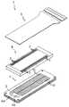
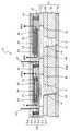
本発明の第1の実施の形態に係る液体圧力発生機構であるアクチュエータユニットを含むインクジェットヘッドについて説明する。図1は、そのインクジェットヘッドの分解斜視図である。図1に示すように、本実施の形態による圧電式のインクジェットヘッド1は、ほぼ直方体の流路ユニット7上にこれとほぼ同形状のアクチュエータユニット6が積層され、アクチュエータユニット6上に外部回路との接続のためのフレキシブルフラットケーブル又はフレキシブルプリント回路(FPC)5が貼付されたものである。インクジェットヘッド1は、流路ユニット7の下面側に開口したノズル9(図2及び図3参照)から下向きにインクを噴射する。
【0039】
アクチュエータユニット6の上面には、FPC5との電気的接続のために用いられる多数の表面電極3が設けられている。また、流路ユニット7の上面には、上方に開口した多数の圧力室(インク収容室)10が設けられている。また、流路ユニット7の長手方向についての一端部近傍には、後述するマニホールド流路15(図3参照)にそれぞれ連通した一対の供給孔4a、4bが穿設されている。供給孔4a、4bは、インクカートリッジ(図示せず)から供給されるインク中の塵除去のためのフィルタ2で覆われている。
【0040】
次に、インクジェットヘッド1の詳細な構造について図2及び図3をさらに参照して説明する。図2は、図1に示すインクジェットヘッドをその長手方向に沿って切断した部分断面図である。図3は、図1に示すインクジェットヘッドをその幅方向に沿って切断した部分断面図である。なお、図2及び図3において、アクチュエータユニット6上のFPC5の図示を省略している。
【0041】
図2及び図3に示すように、インクジェットヘッド1においては、図示されない駆動回路で発生した駆動パルス信号(グランド電位及び正の所定電位のいずれかを選択的にとる)によりFPC5を介して駆動されるアクチュエータユニット6と、インク流路を形成する流路ユニット7とが積層されている。アクチュエータユニット6と流路ユニット7は、エポキシ系の熱硬化性の接着剤によって接着されている。
【0042】
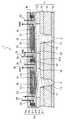
流路ユニット7は、金属材料からなる薄板状の3枚のプレート(キャビティプレート7a、スペーサプレート7b、マニホールドプレート7c)と、インクを噴射するノズル9を備えたポリイミド等の合成樹脂製のノズルプレート7dとが積層されることによって構成されている。最上部のキャビティプレート7aは、アクチュエータユニット6に接している。
【0043】
キャビティプレート7aの表面には、アクチュエータユニット6の動作により選択的に噴射されるインクを収容する複数の圧力室10が長手方向に沿って2列に形成されている。複数の圧力室10は、隔壁10aによって相互に隔てられ、その長手方向を平行に並べて配列されている。また、スペーサプレート7bには、圧力室10の一端をノズル9に連通させる連通孔11と、圧力室10の他端を後述するマニホールド流路15に連通させる連通孔12とがそれぞれ形成されている。
【0044】
また、マニホールドプレート7cには、圧力室10の一端をノズル9に連通させる連通孔13が形成されている。さらに、マニホールドプレート7cには、インクを圧力室10に供給するマニホールド流路15が複数の圧力室10がなす列の下方においてその列方向に長く形成されている。また、マニホールド流路15の一端は、図1に示した一対の供給孔4a、4bのいずれか一方を介して図示されないインク供給源に接続されている。このようにして、マニホールド流路15から連通孔12、圧力室10、連通孔11、連通孔13を経てノズル9に至るインク流路が形成されている。
【0045】
アクチュエータユニット6においては、チタン酸ジルコン酸鉛(PZT)のセラミックス材料からなる6枚の圧電セラミックスプレート6a〜6fが積層されている。そして、圧電セラミックスプレート6bと圧電セラミックスプレート6cとの間、及び、圧電セラミックスプレート6dと圧電セラミックスプレート6eとの間にはそれぞれ共通電極(第2の電極)21、23が、流路ユニット7の圧力室10に対応した範囲内のみに配置されている。なお、共通電極21、23は、各圧電セラミックスプレートのほぼ全範囲を覆う広範囲にわたって配置されてもよい。一方、圧電セラミックスプレート6cと圧電セラミックスプレート6dとの間、及び、圧電セラミックスプレート6eと圧電セラミックスプレート6fとの間にはそれぞれ個別電極(第1の電極)22、24が、流路ユニット7の圧力室10に対応した範囲内にのみ配置されている。
【0046】
共通電極21、23は常にグランド電位に保持されている。一方、個別電極22、24には駆動パルス信号が与えられる。共通電極21、23と個別電極22、24とによって挟まれた圧電セラミックスプレート6c〜6eの当該挟まれた領域は予めこれら電極によって電界が印加されることによって積層方向に分極した活性部25となっている。活性部25は、平面視で圧力室10と同じ方向に延びており且つ圧力室10内に収まる矩形形状を有している(図5参照)。
【0047】
個別電極22、24の電位が正の所定電位になると、圧電セラミックスプレート6c〜6eの活性部25は電界が印加されて積層方向に伸びようとする。ところが、圧電セラミックスプレート6a、6bにはこのような現象が現れないので、アクチュエータユニット6の活性部25に対応した部分は、全体として圧力室10側に伸びるように膨らむ。すると圧力室10の容積が小さくなるので、圧力室10内に充填されたインクに噴射圧力が付与されてノズル9からインクが噴射される。
【0048】
図2に示された2つの圧力室10のうち左側は、このように正の所定電位が与えられて圧力室10側に伸びたアクチュエータユニット6によって圧力室10の容積が縮小することで、当該圧力室10に連通したノズル9からインクが噴射されようとする様子を描いたものである。また、右側は、駆動パルス信号が共通電極21、23の電位と同じくグランド電位に保持されているために、圧力室10に連通したノズル9からインクが噴射されない様子を描いたものである。
【0049】
なお、常態において、全圧力室10に対応する個別電極22、24に電界を印加して、全圧力室10を図2の左側のように縮小しておいて、インクを噴射しようとする圧力室10に対応する個別電極22、24のみ電界を解除して図2の右側のように圧力室10を拡大し、その後再びその個別電極22、24に電界を印加して圧力室10内のインクに圧力を付与する(いわゆる引き打ち)ことによって、インクを噴射することもできる。
【0050】
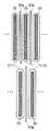
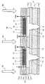
このように、本実施の形態において、アクチュエータユニット6には圧電セラミックスプレート6a〜6fの面方向に対して実質的に垂直な方向(圧電セラミックスプレート6a〜6fの積層方向)に変形可能な複数の活性部25が形成されている。それと共に、アクチュエータユニット6の面方向に隣接する活性部25間は、多数のマイクロクラック(微細な亀裂)が形成されたマイクロクラック領域30となっている。この点について、さらに図4及び図5を参照して説明する。図4は、隣接する活性部25間における図2の拡大図である。図5は、圧力室と活性部とマイクロクラック領域との平面的位置関係を表した模式図である。
【0051】
図2及び図4から分かるように、マイクロクラック領域30は、圧電セラミックスプレート6a〜6fの積層方向について、6枚の圧電セラミックスプレート6a〜6fのうち、3枚の圧電セラミックスプレート6c〜6eだけに形成されている。また、図5から分かるように、マイクロクラック領域30は、圧電セラミックスプレート6a〜6fの面方向について、隣接した活性部25同士を互いに完全に隔絶するように、圧力室10の配列状態と同じく2列に並んだ梯子状に形成されている。
【0052】
マイクロクラック領域30は、3枚の圧電セラミックスプレート6c〜6eのうち、以下に説明する第1のマイクロクラック形成電極(第3の電極)26、28と第2のマイクロクラック形成電極(第4の電極)27、29とが互いに重なり合った領域だけに形成されている。これは、後で説明するように、第1のマイクロクラック形成電極26、28と第2のマイクロクラック形成電極27、29との間に比較的大きな電界を印加することで圧電セラミックスプレート6c〜6eが局所破壊されてマイクロクラックが形成されるからである。アクチュエータユニット6は、マイクロクラック領域30の下方において流路ユニット7の隔壁10aに固定されている。
【0053】
第1のマイクロクラック形成電極26、28は、隣接する活性部25間であって、圧電セラミックスプレート6bと圧電セラミックスプレート6cとの間、及び、圧電セラミックスプレート6dと圧電セラミックスプレート6eとの間にそれぞれが配置されている。一方、第2のマイクロクラック形成電極27、29は、隣接する活性部25間であって、圧電セラミックスプレート6cと圧電セラミックスプレート6dとの間、及び、圧電セラミックスプレート6eと圧電セラミックスプレート6fとの間にそれぞれ配置されている。
【0054】
第1のマイクロクラック形成電極26、28は、共通の端子31に接続されている。第2のマイクロクラック形成電極27、29は、共通の端子32に接続されている。端子31、32は、FPC5側の端子とそれぞれ接続されている。後述するように、インクジェットヘッド1の製造過程において、端子31はグランド電位に固定され且つ端子32には比較的大きな正の電位が一時的に付与される。
【0055】
このように、本実施の形態による液体圧力発生機構であるアクチュエータユニット6によると、隣接する2つの活性部25の間において圧電セラミックスプレート6c〜6eにマイクロクラック領域30が設けられているので、インク噴射時に隣接する活性部25への変位の伝播が一部遮断されて隣接する活性部25同士のクロストークを低減することができる。したがって、高い印刷品質での印刷が可能となる。
【0056】
特に、本実施の形態の場合、図5に示すように、マイクロクラック領域30が隣接した活性部25同士を面方向について互いに完全に隔絶しているので、大幅なクロストークの低減効果が期待できる。ただし、図5に示すように活性部25同士をマイクロクラック領域30で完全に隔絶するようにすると共通電極21、23の配線を共通にすることができなくなって配線構造が複雑になってしまうという問題が生じる。そこで、一変形例として、マイクロクラック領域30が隣接する活性部25の間のどこか一部分で分断されるようにし、そこに共通電極21、23を通して隣接する活性部25に係る共通電極21、23と接続するようにすればクロストーク低減効果はやや低下するものの配線構造が複雑になることがなくなる。また、別の変形例として、図5と同様の模式図である図6に示すように、それぞれが矩形形状を有する多数のマイクロクラック領域30aがアクチュエータユニット6の長手方向に隣接する活性部25の間にそれぞれ設けられてもよい。図6のようにマイクロクラック領域30aを設けた場合でも、図5の場合よりは劣るものの優れたクロストーク低減効果が得られる。
【0057】
また、後で説明する製造方法からも明らかなように、マイクロクラック領域30は圧電セラミックスプレート6c〜6eの積層方向に延在した溝を形成する場合のようにダイヤモンドカッタを用いなくても形成可能であるので、容易且つ短時間に製造することができる。
【0058】
さらに、本実施の形態によるアクチュエータユニット6によると、クロストークが低減されるために圧電セラミックスプレートを従来よりも数多く積層することが可能となり、これにより圧電セラミックスプレート1枚あたりの変位量が少なくても全体として大きな変位量を得ることができるようになって個別電極22、24の低電圧駆動が可能となる。そのため、個別電極22、24の駆動パルス信号を発生する回路部品のコストダウンが可能となる。
【0059】
しかも、本実施の形態によるアクチュエータユニット6によると、後で説明する製造方法からも明らかなように、第1のマイクロクラック形成電極26、28と第2のマイクロクラック形成電極27、29との電位を異なるものとすることでこれら2つの電極の間に電界を印加することができるので、極めて容易に圧電セラミックスプレート6c〜6eにマイクロクラックを形成可能である。
【0060】
さらに、本実施の形態によるアクチュエータユニット6においては積層された複数の圧電セラミックスプレート6b〜6fの間に共通電極21、23と個別電極22、24とが積層方向に交互に配置されていると共に圧電セラミックスプレート6b〜6fの間に第1のマイクロクラック形成電極26、28と第2のマイクロクラック形成電極27、29とが積層方向に交互に配置されているので、圧電セラミックスプレート6c〜6eのそれぞれが第1のマイクロクラック形成電極26、28と第2のマイクロクラック形成電極27、29とによって挟まれることになる。そのため、後で説明する製造方法からも明らかなように、電極間距離が比較的小さくなって、マイクロクラック形成の際に第2のマイクロクラック形成電極27、29に非常に大きな電位を与える必要がなくなる。また、3枚の圧電セラミックスプレート6c〜6eにマイクロクラック領域30を形成することができるので、1枚の圧電セラミックスプレートだけにマイクロクラックを形成する場合と比較して活性部25間のクロストークを効果的に低減することができる。
【0061】
また、本実施の形態によるインクジェットヘッド1は、アクチュエータユニット6がマイクロクラック領域30の下方において流路ユニット7の隔壁10aに固定されたものである。そのため、活性部25の変形を圧力室10の容積変化として有効に使用できるので、良好なエネルギー効率が得られるという利点がある。
【0062】
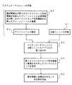
次に、本実施の形態によるアクチュエータユニットを含むインクジェットヘッド1の製造方法についてその工程図である図7を参照しつつ説明する。図1〜図5で説明したようなインクジェットヘッド1を製造するには、流路ユニット7及びアクチュエータユニット6などの部品を別々に作製し、それから各部品を組み付ける。
【0063】
流路ユニット7を作製するには、図2に描かれた4枚のプレート7a〜7dをそれぞれ独立して作製した後に、これらが位置合わせされて積層された状態で接着剤を用いてこれらを互いに接着する。なお、プレート7a〜7cに圧力室10や連通孔11などを形成するのにはエッチング加工が用いられ、プレート7dにノズル9を形成するのにはレーザ加工が用いられる(ステップS1)。
【0064】
一方、アクチュエータユニット6を作製するには、まず、個別電極22、24及び第2のマイクロクラック形成電極27、29が導電性ペーストでそれぞれスクリーン印刷された圧電セラミックスのグリーンシート2枚と、共通電極21、23及び第1のマイクロクラック形成電極26、28が導電性ペーストでそれぞれスクリーン印刷された圧電セラミックスのグリーンシート2枚とを交互に積層し、さらにその上に、何も印刷されていない圧電セラミックスのグリーンシート1枚と、表面電極3が導電性ペーストでスクリーン印刷された圧電セラミックスのグリーンシート1枚とを順次積層する(ステップS2)。これによって、アクチュエータユニット6となる電極複合体が得られる。
【0065】
そして、ステップS2で得られた電極複合体を公知のセラミックスと同様に脱脂し、所定の温度で焼成する(ステップS3)。これにより、上述したようなアクチュエータユニット6を比較的容易に作製することができる。なお、アクチュエータユニット6は、予め焼成による収縮量を見込んで設計される。
【0066】
しかる後、流路ユニット7とアクチュエータユニット6とが、活性部25の位置と圧力室10の位置とを合わせて、熱硬化性接着剤を用いて貼り合わされると共に、アクチュエータユニット6と別途用意されたFPC5とが表面電極3とこれに対応するFPC5上の電極とがそれぞれ重なるように半田を用いて貼り合わされる(ステップS4)。なお、このFPC5の貼り合わせは、後述するステップS5の後で行ってもよい。この場合、マイクロクラック形成電極26〜29への電界の印加はFPC5とは別の手段で行われる。
【0067】
その後、第1のマイクロクラック形成電極26、28の電位をグランド電位に保持した状態においてFPC5から第2のマイクロクラック形成電極27、29に高電位を与えることで、第1のマイクロクラック形成電極26、28と第2のマイクロクラック形成電極27、29とによって挟まれた部分の圧電セラミックスプレート6c〜6eにその絶縁破壊限界を超える高い電界(例えば、インク噴射動作時に印加される電界の8〜30倍である6.4kV/mm〜24kV/mm程度以上)を印加する。これによって、当該部分は局所的な絶縁破壊により多数のマイクロクラックが形成されたマイクロクラック領域30となる(ステップS5)。
【0068】
そして、共通電極21、23の電位をグランド電位に保持した状態においてFPC5から個別電極22、24に高電位(ステップS5で第2のマイクロクラック形成電極27、29に与えられるよりも低い電位)を与えることで、共通電極21、23と個別電極22、24とによって挟まれた部分の圧電セラミックスプレート6c〜6eにその絶縁破壊限界を超えない高い電界(例えば、インク噴射動作時に印加される電界の2〜8倍である1.6kV/mm〜6.4kV/mm程度)を印加する。これによって、当該部分は分極されて、インク噴射動作時に圧電セラミックスプレート6c〜6eの面方向に対して実質的に垂直な方向に変形可能な活性部25となる(ステップS6)。以上の工程を経ることによって、インクジェットヘッド1が完成する。
【0069】
上述した製造方法には、第1のマイクロクラック形成電極26、28と第2のマイクロクラック形成電極27、29との間の圧電セラミックスプレート6c〜6eに高い電界を印加することで極めて短時間にマイクロクラックを形成可能であるという利点がある。また、高い位置精度でマイクロクラックを形成することができるという利点もある。さらに、加工後に洗浄工程が不要であるので、上述したように機械加工で活性部25間に溝を作る場合に比較して、容易且つ短時間にクロストークが低減されたアクチュエータユニット6を作製可能である。
【0070】
なお、ここではアクチュエータユニット6と流路ユニット7とを貼り合わせてから活性部25及びマイクロクラック領域30を形成したが、活性部25及びマイクロクラック領域30を形成してからアクチュエータユニット6と流路ユニット7とを貼り合わせてもよい。また、ステップS5のマイクロクラック形成工程とステップS6の活性部形成工程とは順序を入れ替えて行っても何ら支障はない。
【0071】
[第2の実施の形態]
次に、本発明の第2の実施の形態に係る液体圧力発生機構であるアクチュエータユニットを含むインクジェットヘッドについて図8を参照して説明する。図8は、図2と同様にインクジェットヘッドをその長手方向に沿って切断した部分断面図である。なお、本実施の形態において第1の実施の形態と同一の部材については、同一の符号を付してその説明を省略する。
【0072】
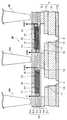
図8に示すインクジェットヘッド41では、アクチュエータユニット46に含まれる圧電セラミックスプレート6c上の共通電極43(グランド電位に保持されている)は、面方向に隣接する一方の活性部25との中間付近にまで延在している。面方向に隣接する2つの活性部25の間には、1枚の第1のマイクロクラック形成電極(第3の電極)42が圧電セラミックスプレート6fの下側に配置されているだけで、上述した第1の実施の形態のようにこれと対になる第2のマイクロクラック形成電極は設けられていない。そして、共通電極43の図8中右側への延在部分と第1のマイクロクラック形成電極42とによって挟まれた4枚の圧電セラミックスプレート6c〜6fの当該挟まれた領域だけがマイクロクラック領域44となっている。第1のマイクロクラック形成電極42は端子47に接続されている。インクジェットヘッド41は、ここで説明した以外は、第1の実施の形態で説明したインクジェットヘッド1と同様に構成されている。
【0073】
図8に示したインクジェットヘッド41の製造手順は図7で説明したのと概ね同様である。ただし、本実施の形態の場合、ステップS5において端子47を介して第1のマイクロクラック形成電極42に高電位が与えられる。すると、第1のマイクロクラック形成電極42と共通電極43との間に高電界が印加され、両者に挟まれた部分がマイクロクラック領域44となる。
【0074】
本実施の形態による液体圧力発生機構であるアクチュエータユニット46によると、第1の実施の形態と同様に、隣接する2つの活性部25の間において4枚の圧電セラミックスプレート6c〜6fにマイクロクラック領域44が設けられているので、インク噴射時に隣接する活性部25への変位の伝播が一部遮断されて隣接する活性部25同士のクロストークを低減することができる。したがって、高い印刷品質での印刷が可能となる。そのほか、第1の実施の形態で得られたのと同様の効果が得られる。
【0075】
ただし、本実施の形態によるアクチュエータユニット46においてはマイクロクラック領域44が形成された圧電セラミックスプレート6c〜6f間にそれぞれマイクロクラック形成電極が配置されておらず、これら4枚の圧電セラミックスプレート6c〜6f群の両側だけにこれらプレート群を挟み込む電極42、43が配置されているだけである。そのため、電極間距離が大きくなるので、第1のマイクロクラック形成電極42に与える電位を第1の実施の形態において第2のマイクロクラック形成電極27、29に与えられる電位の数倍程度の非常に高いものとする必要がある。
【0076】
また、本実施の形態によると、第1のマイクロクラック形成電極42と対になる第2のマイクロクラック形成電極を設ける必要がないために、アクチュエータユニット46内部の配線構造が簡略化できる。したがって、アクチュエータユニット46の製造が容易となる。
【0077】
さらに、本実施の形態の場合、第1のマイクロクラック形成電極42が1枚だけ設けられており、これに対応して2枚の共通電極23、43のうち1枚だけが隣接する活性部25との中間付近にまで延在していることで、4枚の圧電セラミックスプレート6c〜6fが第1のマイクロクラック形成電極42と共通電極43とによって挟まれることになる。つまり、マイクロクラック領域44が第1の実施の形態よりも多くの枚数の圧電セラミックスプレートに跨って形成されているために、より優れたクロストーク低減効果が得られる。しかも、第1のマイクロクラック形成電極が2枚設けられ且つ2枚の共通電極が隣接する一方の活性部25との中間付近にまで延在している場合と比較して構造が簡略化されるため、構造が簡単で歩留まりが向上するという利益が得られる。
【0078】
なお、本実施の形態では共通電極43を隣接する活性部25との中間付近にまで延在させているが、その代わりとして個別電極を隣接する活性部25との中間付近にまで延在させてもよい。その場合、マイクロクラック領域44を形成する際に、当該延在させた個別電極に高電位が与えられ且つ第1のマイクロクラック形成電極42はグランド電位に保持される。
【0079】
[第3の実施の形態]
次に、本発明の第3の実施の形態に係る液体圧力発生機構であるアクチュエータユニットを含むインクジェットヘッドについて図9を参照して説明する。図9は、図2と同様にインクジェットヘッドをその長手方向に沿って切断した部分断面図である。なお、本実施の形態において第1の実施の形態と同一の部材については、同一の符号を付してその説明を省略する。
【0080】
図9に示すインクジェットヘッド51において、アクチュエータユニット56内の隣接する活性部25間に、上述した第1及び第2の実施の形態とは異なり、マイクロクラック形成電極は配置されていない。それにも拘わらず、面方向に隣接する活性部25間の5枚の圧電セラミックスプレート6a〜6eにはマイクロクラック領域54が形成されている。これは、上述した第1及び第2の実施の形態とは異なる方法でマイクロクラック領域54が形成されていることを意味する。インクジェットヘッド51は、ここで説明した以外は、第1の実施の形態で説明したインクジェットヘッド1と同様に構成されている。
【0081】
本実施の形態による液体圧力発生機構であるアクチュエータユニット56によると、第1及び第2の実施の形態と同様に、隣接する2つの活性部25の間において5枚の圧電セラミックスプレート6a〜6eにマイクロクラック領域44が設けられているので、インク噴射時に隣接する活性部25への変位の伝播がかなり遮断されて隣接する活性部25同士のクロストークを大幅に低減することができる。したがって、高い印刷品質での印刷が可能となる。そのほか、第1の実施の形態で得られたのと同様の効果が得られる。
【0082】
次に、図9に示したインクジェットヘッド51の製造方法について、第1の実施の形態との相違点を中心に説明する。
【0083】
まず、図7のステップS2で第1及び第2のマイクロクラック形成電極となる導電性ペーストをグリーンシート上に印刷せず、共通電極21、23及び個別電極22、24となる導電性ペーストをグリーンシート上に印刷する。
【0084】
その後、ステップS3のグリーンシートの焼成工程後にできたアクチュエータユニット56と、ステップS1で作製された流路ユニット7とをステップS4で貼り合わせる。これにより、マイクロクラック領域54及び活性部25が形成されていない以外は図9に示すインクジェットヘッド51と同様に構成された、図10に示すインクジェットヘッド51になるべき構造物58が得られる。
【0085】
その後、ステップS5で、図11に示すように、圧電セラミックスプレート6aの表面の面方向に隣接する活性部25間にレーザビーム59を照射する。このとき、レーザビーム59のレーザ源としては例えばYAGレーザのように被照射物に熱を加えることができるものが用いられ、そのレーザ照射条件は、例えば、ノーマルパルスYAGレーザ(1.06μm)、照射エネルギー1〜10J、パルス幅0.2〜2msである。このレーザ照射によって、面方向に隣接する活性部25間の圧電セラミックスプレート6a〜6dにはマイクロクラック領域54が形成される。
【0086】
その後、アクチュエータユニット56上にFPC5を貼り合わせ、ステップS6でFPC5を介して個別電極22、24に高電位を与えることで、圧電セラミックスプレート6c〜6eに活性部25を形成する。このような工程を経ることで、図9に示したようなインクジェットヘッド51を製造することができる。
【0087】
なお、本実施の形態の製造方法において、ステップS5でレーザビーム59を照射する代わりとして、図12に示すように、圧電セラミックスプレート6aの表面の面方向に隣接する活性部25間を圧子60で押圧してもよい。このとき、圧子60としては例えば先端に人造ダイヤモンドが配置されたものが用いられ、その押圧条件は、例えば、マイクロビッカース圧子において荷重50〜500gfである。このように圧子60での押圧によっても、面方向に隣接する活性部25間の圧電セラミックスプレート6a〜6dにマイクロクラック領域54を形成することができる。
【0088】
本実施の形態による製造方法によると、高い位置精度でマイクロクラックを形成することができる。さらに、加工後に洗浄工程が不要であるので、上述したように機械加工で活性部25間に溝を作る場合に比較して、容易且つ短時間にクロストークが低減されたアクチュエータユニット56を作製可能である。
【0089】
なお、上述した第1及び第2の実施の形態のように高電界を印加することで形成されたマイクロクラックと、レーザビーム59を照射することで形成されたマイクロクラックと、圧子60で押圧することで形成されたマイクロクラックとは、その構造(クラックの長さやクラック間の間隙、クラック密度など)が異なるが、いずれの方法によって形成されたマイクロクラックも十分なクロストーク低減効果を発揮することが本発明者によって確認されている。
【0090】
以上、本発明の好適な実施の形態について説明したが、本発明は、上述した実施の形態に限定されるものではなく、特許請求の範囲に記載した限りにおいてさまざまな変更が可能なものである。例えば、上述した実施の形態以外の方法で隣接する活性部間にマイクロクラック領域が形成されてもよい。また、マイクロクラック領域は必ずしも隣接する活性部間を遮断するように連続的に形成されている必要はなく、不連続的に形成されていてもよい。
【0091】
また、上述した実施の形態では複数枚の圧電セラミックスプレートに跨ってマイクロクラック領域が形成されているが、マイクロクラック領域は1枚の圧電セラミックスプレートにだけ形成されていてもよい。同様に、活性部も1枚の圧電セラミックスプレートにだけ形成されていてよい。また、アクチュエータユニット内における圧電セラミックスプレートの積層数は複数枚に限らず、1枚だけであってもよい。
【0092】
また、上述した実施の形態で説明したインクジェットプリンタと同様に構成された液滴噴射装置において、噴射媒体として導電ペーストを用いることにより、極めて微細な電気回路パターンを印刷したり、或いは、噴射媒体として有機発光体を用いることにより有機エレクトロルミネッセンスディスプレイ(OELD)などの高精細ディスプレイデバイスを作成したりすることもできる。そのほか、上述した実施の形態で説明したインクジェットプリンタと同様に構成された液滴噴射装置は、微小なドットを被印刷媒体上に形成する用途であれば、極めて広範に用いることができる。
【0093】
【発明の効果】
以上説明したように、本発明によると、隣接する2つの活性部の間において板状体にマイクロクラックが形成されているので、活性部間のクロストークを低減することができる。また、マイクロクラックは板状体の積層方向に延在した溝を形成する場合のようにダイヤモンドカッタを用いなくても形成可能であるので、容易且つ短時間に製造することができる。さらに、クロストークが低減されるために板状体を従来よりも数多く積層することが可能となり、これにより板状体1枚あたりの変位量が少なくても全体として大きな変位量を得ることができるようになって第1の電極又は第2の電極の低電圧駆動が可能となる。そのため、第1の電極又は第2の電極の駆動信号を発生する回路部品のコストダウンが可能となる。
【0094】
また、本発明によると、高い位置精度でマイクロクラックを形成することができ、しかも加工後に洗浄工程が不要となって機械加工で活性部間に溝を作る場合に比較して容易且つ短時間にクロストークが低減された液体圧力発生機構を製造可能となる。
【0095】
また、本発明によると、活性部の変形を液体収容室の容積変化として有効に使用できるので、良好なエネルギー効率が得られる。
【図面の簡単な説明】
【図1】 本発明の第1の実施の形態に係る液体圧力発生機構であるアクチュエータユニットを含むインクジェットヘッドの分解斜視図である。
【図2】 図1に示すインクジェットヘッドをその長手方向に沿って切断した部分断面図である。
【図3】 図1に示すインクジェットヘッドをその幅方向に沿って切断した部分断面図である。
【図4】 隣接する活性部間における図2の拡大図である。
【図5】 圧力室と活性部とマイクロクラック領域との平面的位置関係を表した模式図である。
【図6】 図5の変形例を示す模式図である。
【図7】 図1に示すインクジェットヘッドの製造方法を示す工程図である。
【図8】 本発明の第2の実施の形態に係る液体圧力発生機構であるアクチュエータユニットを含むインクジェットヘッドをその長手方向に沿って切断した部分断面図である。
【図9】 本発明の第3の実施の形態に係る液体圧力発生機構であるアクチュエータユニットを含むインクジェットヘッドをその長手方向に沿って切断した部分断面図である。
【図10】 図9に示すインクジェットヘッドの一製造工程を描いた断面図である。
【図11】 図9に示すインクジェットヘッドの一製造工程を描いた断面図である。
【図12】 図11に示したものの変形例として、図9に示すインクジェットヘッドの一製造工程を描いた断面図である。
【図13】 従来のインクジェットヘッドをその長手方向に沿って切断した部分断面図である。
【符号の説明】
1 インクジェットヘッド(流体圧力発生機構)
5 FPC
6 アクチュエータユニット
6a〜6f 圧電セラミックスプレート
7 流路ユニット
9 ノズル
10 圧力室(液体収容室)
10a 隔壁
21、23 共通電極(第2の電極)
22、24 個別電極(第1の電極)
25 活性部
26、28 第1のマイクロクラック形成電極(第3の電極)
27、29 第2のマイクロクラック形成電極(第4の電極)
30 マイクロクラック領域[0001]
BACKGROUND OF THE INVENTION
The present inventionIn a method for manufacturing a droplet ejecting apparatus that ejects droplets from a nozzle by applying pressure to a liquid in a liquid storage chamberRelated.
[0002]
[Prior art]
A piezo method is known as an example of a liquid pressure generating mechanism used for applying pressure to ink stored in a pressure chamber in an inkjet head (
[0003]
The
[0004]
On the surface of the
[0005]
The
[0006]
In the
[0007]
The
[0008]
In the left side of the two
[0009]
In the
[0010]
Therefore, a technique is known in which crosstalk is reduced by forming grooves (slits) extending in the stacking direction of piezoelectric ceramic plates in an actuator unit between active portions using a diamond cutter (Patent Document). 3).
[0011]
[Patent Document 1]
Japanese Patent Laying-Open No. 2002-59547 (FIG. 11)
[Patent Document 2]
Japanese Patent Laid-Open No. 2002-127420 (FIG. 6)
[Patent Document 3]
Japanese Patent Publication No. 7-33087 (FIGS. 1 and 2)
[0012]
[Problems to be solved by the invention]
However, in the technique described in the above publication (Patent Document 3), it is not only very complicated to form a groove extending in the stacking direction of the piezoelectric ceramic plate by using a diamond cutter, but also a groove forming step. There is a problem that good manufacturing efficiency cannot be obtained because a cleaning process is required later and a long time is required.
[0013]
The present invention has been made in view of the above problems, and can be manufactured easily and in a short time with reduced crosstalk.liquidDroplet ejector including body pressure generating mechanismManufacturing methodThe purpose is to provide.
[0014]
[Means for Solving the Problems]
[0015]
[0016]
[0017]
[0018]
[0019]
[0020]
[0021]
[0022]
[0023]
[0024]
[0025]
[0026]
[0027]
[0028]
[0029]
The present inventionA plurality of nozzles for ejecting liquid droplets, a channel unit in which a liquid channel including a plurality of liquid storage chambers communicating with the plurality of nozzles is formed, and a piezoelectric element disposed across the plurality of liquid storage chambers A plate-like body made of a material, and a first electrode and a second electrode arranged so as to sandwich a portion of the plate-like body facing the plurality of liquid storage chambers. A method for manufacturing a liquid droplet ejecting apparatus, comprising: a liquid pressure generating mechanism configured to deform a portion facing the liquid storage chamber in a direction substantially perpendicular to the surface direction to apply pressure to the liquid in the liquid storage chamberA flow path unit forming step for forming the flow path unit, and the first electrode and the first electrode so that the plate-like body is sandwiched between portions of the plate-like body facing the plurality of liquid storage chambers. An electrode composite in which two electrodes are formed and a third electrode and a fourth electrode are formed so that the plate-like body is sandwiched between portions of the plate-like body facing the partition walls separating the plurality of liquid storage chambers A voltage is applied between the third electrode and the fourth electrode after the joining step, and the joining step of joining the flow path unit and the electrode composite. A microcrack forming step for forming a microcrack on a portion of the plate-like body facing the partition wall by generating an electric field exceeding the dielectric breakdown limit of the plate-like body, and after the microcrack forming step, The first electrode By applying a voltage between the second electrode and generating an electric field that does not exceed the dielectric breakdown limit of the plate-like body, the portions of the plate-like body facing the liquid storage chambers are polarized. And a polarization step to be performed (Claim 1).
[0030]
According to this configuration, since micro cracks are formed in the plate-like body between two adjacent active portions, crosstalk can be reduced. Unlike the case of forming a groove extending in the laminating direction of the plate-like body, the microcrack can be formed without using a diamond cutter, and can be manufactured easily and in a short time. Furthermore, since crosstalk is reduced, it becomes possible to stack a larger number of plate-like bodies than before, and thereby a large displacement amount as a whole can be obtained even if the displacement amount per plate-like body is small. Thus, the first electrode or the second electrode can be driven at a low voltage. Therefore, it is possible to reduce the cost of the circuit component that generates the drive signal for the first electrode or the second electrode.
Note that the microcracks are preferably formed over the entire thickness of the plate-like body or over the entire thickness of the active portion, but are only formed over at least a portion of the total thickness of the active portion. But you can. Moreover, although it is preferable that the microcracks are continuously formed in a strip shape so as to separate the active parts adjacent to each other, the microcracks may be formed discontinuously between the active parts adjacent to each other.
Also,According to this configuration, a microcrack can be formed in a very short time by applying an electric field to the plate-like body between the third electrode and the fourth electrode. In addition, microcracks can be formed with high positional accuracy, and a cross-talk can be reduced easily and in a short time compared to the case where grooves are formed between active parts by machining because a cleaning step is not required after processing. A liquid pressure generating mechanism can be manufactured.
In the method for manufacturing a droplet ejecting apparatus of the present invention, a plurality of the plate-like bodies are stacked in the electrode complex forming step, and the first electrode and the second electrode are interposed between the plate-like bodies. Are alternately arranged in the stacking direction, and the third electrode and the fourth electrode may be arranged with their plate-like bodies interposed therebetween (Claim 2).
According to this, since each plate-like body is sandwiched between the third electrode and the fourth electrode, the distance between the electrodes can be made relatively small, so that it is not necessary to use a large voltage when forming the microcracks. . In addition, since microcracks can be formed in many plate-like bodies, crosstalk can be effectively reduced.
[0031]
AnotherFrom the point of view of the present invention, the present inventionA plurality of nozzles for ejecting liquid droplets, a channel unit in which a liquid channel including a plurality of liquid storage chambers communicating with the plurality of nozzles is formed, and a piezoelectric element disposed across the plurality of liquid storage chambers A plate-like body made of a material, and a first electrode and a second electrode arranged so as to sandwich a portion of the plate-like body facing the plurality of liquid storage chambers. A method of manufacturing a droplet ejecting apparatus, comprising: a liquid pressure generating mechanism that applies a pressure to the liquid in the liquid storage chamber by deforming a portion facing the liquid storage chamber in a direction substantially perpendicular to the surface direction thereof. A flow path unit forming step for forming the flow path unit; and the first electrode and the second electrode so as to sandwich the plate-like body between portions of the plate-like body facing the plurality of liquid storage chambers. And the first electrode One of the second electrodes extends to a portion facing the partition separating the liquid storage chamber, and a portion of the plate-like body facing the partition is connected to the one of the first electrode and the second electrode. The third electrode is shaped so as to sandwich itAn electrode composite forming step for forming the formed electrode composite, a joining step for joining the flow path unit and the electrode composite, and after the joining step, the third electrode, the first electrode, and the By applying a voltage between the one of the second electrodes and generating an electric field exceeding the dielectric breakdown limit of the plate-like body, a microcrack is formed in a portion of the plate-like body facing the partition wall. After the microcrack forming step and the microcrack forming step, a voltage is applied between the first electrode and the second electrode to generate an electric field that does not exceed the dielectric breakdown limit of the plate-like body. And a polarization step of polarizing portions of the plate-like body facing the plurality of liquid storage chambers.(Claims3).
[0032]
According to this configuration, since micro cracks are formed in the plate-like body between two adjacent active portions, crosstalk can be reduced. Unlike the case of forming a groove extending in the laminating direction of the plate-like body, the microcrack can be formed without using a diamond cutter, and can be manufactured easily and in a short time. Furthermore, since crosstalk is reduced, it becomes possible to stack a larger number of plate-like bodies than before, and thereby a large displacement amount as a whole can be obtained even if the displacement amount per plate-like body is small. Thus, the first electrode or the second electrode can be driven at a low voltage. Therefore, it is possible to reduce the cost of the circuit component that generates the drive signal for the first electrode or the second electrode.
Note that the microcracks are preferably formed over the entire thickness of the plate-like body or over the entire thickness of the active portion, but are only formed over at least a portion of the total thickness of the active portion. But you can. Moreover, although it is preferable that the microcracks are continuously formed in a strip shape so as to separate the active parts adjacent to each other, the microcracks may be formed discontinuously between the active parts adjacent to each other.
In addition, according to this configuration, either the first electrode or the second electrode extending between two adjacent active portions so as to face the third electrode across the plate-like body and the third electrode Since a microcrack can be formed by applying an electric field between the electrode and the electrode, the fourth electrode becomes unnecessary. Therefore, the wiring structure to the electrode can be simplified.
Also,According to this configuration, the third electrode andOne of the first electrode and the second electrodeA microcrack can be formed in a very short time by applying an electric field to the plate-like body between the two. In addition, microcracks can be formed with high positional accuracy, and a cross-talk can be reduced easily and in a short time compared to the case where grooves are formed between active parts by machining because a cleaning step is not required after processing. A liquid pressure generating mechanism can be manufactured.
In the method for manufacturing a droplet ejecting apparatus of the present invention, in the step of forming the electrode composite, a plurality of the plate-like bodies are stacked, and the first electrode and the second electrode are sandwiched between the plate-like bodies. The electrodes may be alternately arranged in the stacking direction, and the third electrode and the one of the first electrode and the second electrode may be arranged with their plate-like bodies interposed therebetween (Claim 4). .
According to this, since the number of the third electrodes is small, the structure is simple and the yield is improved.
[0033]
In another aspect, the present invention provides:A plurality of nozzles for ejecting liquid droplets, a channel unit in which a liquid channel including a plurality of liquid storage chambers communicating with the plurality of nozzles is formed, and a piezoelectric element disposed across the plurality of liquid storage chambers A plate-like body made of a material, and a first electrode and a second electrode arranged so as to sandwich a portion of the plate-like body facing the plurality of liquid storage chambers. A method of manufacturing a droplet ejecting apparatus, comprising: a liquid pressure generating mechanism that applies a pressure to the liquid in the liquid storage chamber by deforming a portion facing the liquid storage chamber in a direction substantially perpendicular to the surface direction thereof. A flow path unit forming step for forming the flow path unit; and the first electrode and the second electrode so as to sandwich the plate-like body between portions of the plate-like body facing the plurality of liquid storage chambers. The electrode composite forming the electrode composite with A body forming step, a joining step for joining the flow path unit and the electrode assembly, and a microcrack forming step for forming microcracks in a portion of the plate-like body facing the partition after the joining step; After the microcrack forming step, a voltage is applied between the first electrode and the second electrode.And a polarization step of polarizing portions of the plate-like body facing the plurality of liquid storage chambers by generating an electric field that does not exceed a dielectric breakdown limit of the plate-like body.The aboveMicrocrack formation processSaidExceeding its dielectric breakdown limit to a plateBy applying an electric field,MaA microcrack may be formed (claim)6). Also, the aboveMicrocrack formation processSaidPlateBy irradiating a laser beam onMaA microcrack may be formed (claim)7).
[0034]
In addition,Microcrack formation processSaidPlateBy pressing the surface of theMaA microcrack may be formed (claim)8).
[0035]
According to these configurations, since micro cracks are formed in the plate-like body between two adjacent active portions, crosstalk can be reduced. Unlike the case of forming a groove extending in the laminating direction of the plate-like body, the microcrack can be formed without using a diamond cutter, and can be manufactured easily and in a short time. Furthermore, since crosstalk is reduced, it becomes possible to stack a larger number of plate-like bodies than before, and thereby a large displacement amount as a whole can be obtained even if the displacement amount per plate-like body is small. Thus, the first electrode or the second electrode can be driven at a low voltage. Therefore, it is possible to reduce the cost of the circuit component that generates the drive signal for the first electrode or the second electrode.
Note that the microcracks are preferably formed over the entire thickness of the plate-like body or over the entire thickness of the active portion, but are only formed over at least a portion of the total thickness of the active portion. But you can. Moreover, although it is preferable that the microcracks are continuously formed in a strip shape so as to separate the active parts adjacent to each other, the microcracks may be formed discontinuously between the active parts adjacent to each other.
Also,According to these configurations, microcracks can be formed with high positional accuracy, and a cleaning process is not required after processing, and crossing is easier and shorter than when grooves are formed between active portions by machining. A liquid pressure generating mechanism with reduced talk can be manufactured.
[0036]
[0037]
DETAILED DESCRIPTION OF THE INVENTION
Hereinafter, preferred embodiments of the present invention will be described with reference to the drawings.
[0038]
[First Embodiment]
An ink jet head including an actuator unit that is a liquid pressure generating mechanism according to a first embodiment of the present invention will be described. FIG. 1 is an exploded perspective view of the inkjet head. As shown in FIG. 1, the piezoelectric
[0039]
A large number of
[0040]
Next, the detailed structure of the
[0041]
As shown in FIGS. 2 and 3, the
[0042]
The
[0043]
On the surface of the
[0044]
The
[0045]
In the
[0046]
The
[0047]
When the potentials of the
[0048]
The left side of the two
[0049]
In a normal state, an electric field is applied to the
[0050]
Thus, in the present embodiment, the
[0051]
As can be seen from FIGS. 2 and 4, the
[0052]
Among the three piezoelectric ceramic plates 6c to 6e, the
[0053]
The first micro
[0054]
The first
[0055]
As described above, according to the
[0056]
In particular, in the case of the present embodiment, as shown in FIG. 5, since the
[0057]
Further, as is apparent from the manufacturing method described later, the
[0058]
Furthermore, according to the
[0059]
Moreover, according to the
[0060]
Further, in the
[0061]
In addition, in the
[0062]
Next, the manufacturing method of the
[0063]
In order to fabricate the
[0064]
On the other hand, to produce the
[0065]
Then, the electrode composite obtained in step S2 is degreased in the same manner as known ceramics and fired at a predetermined temperature (step S3). Thereby, the
[0066]
Thereafter, the
[0067]
Thereafter, a high potential is applied from the
[0068]
Then, in a state where the potentials of the
[0069]
In the manufacturing method described above, a high electric field is applied to the piezoelectric ceramic plates 6c to 6e between the first
[0070]
Here, the
[0071]
[Second Embodiment]
Next, an ink jet head including an actuator unit which is a liquid pressure generating mechanism according to a second embodiment of the present invention will be described with reference to FIG. FIG. 8 is a partial cross-sectional view of the ink jet head cut along the longitudinal direction thereof as in FIG. In addition, in this Embodiment, about the member same as 1st Embodiment, the same code | symbol is attached | subjected and the description is abbreviate | omitted.
[0072]
In the
[0073]
The manufacturing procedure of the
[0074]
According to the
[0075]
However, in the
[0076]
In addition, according to the present embodiment, it is not necessary to provide the second microcrack forming electrode that is paired with the first
[0077]
Furthermore, in the case of the present embodiment, only one first
[0078]
In the present embodiment, the
[0079]
[Third Embodiment]
Next, an ink jet head including an actuator unit which is a liquid pressure generating mechanism according to a third embodiment of the present invention will be described with reference to FIG. FIG. 9 is a partial cross-sectional view of the ink jet head cut along the longitudinal direction thereof as in FIG. In addition, in this Embodiment, about the member same as 1st Embodiment, the same code | symbol is attached | subjected and the description is abbreviate | omitted.
[0080]
In the
[0081]
According to the
[0082]
Next, a method for manufacturing the
[0083]
First, in step S2 of FIG. 7, the conductive paste to be the first and second microcrack forming electrodes is not printed on the green sheet, but the conductive paste to be the
[0084]
Thereafter, the
[0085]
Thereafter, in step S5, as shown in FIG. 11, a
[0086]
Thereafter, the
[0087]
In the manufacturing method of the present embodiment, instead of irradiating the
[0088]
According to the manufacturing method of the present embodiment, microcracks can be formed with high positional accuracy. Furthermore, since a cleaning step is not required after processing, the
[0089]
The microcracks formed by applying a high electric field as in the first and second embodiments described above, the microcracks formed by irradiating the
[0090]
The preferred embodiments of the present invention have been described above. However, the present invention is not limited to the above-described embodiments, and various modifications are possible as long as they are described in the claims. . For example, a microcrack region may be formed between adjacent active portions by a method other than the embodiment described above. Further, the microcrack region does not necessarily have to be formed continuously so as to block between adjacent active portions, and may be formed discontinuously.
[0091]
In the embodiment described above, the microcrack region is formed across a plurality of piezoelectric ceramic plates. However, the microcrack region may be formed only on one piezoelectric ceramic plate. Similarly, the active portion may be formed only on one piezoelectric ceramic plate. Further, the number of stacked piezoelectric ceramic plates in the actuator unit is not limited to a plurality, and may be only one.
[0092]
In addition, in the liquid droplet ejecting apparatus configured in the same manner as the ink jet printer described in the above-described embodiment, by using a conductive paste as the ejecting medium, an extremely fine electric circuit pattern can be printed or the ejecting medium can be used. A high-definition display device such as an organic electroluminescence display (OELD) can also be created by using an organic light emitter. In addition, the droplet ejecting apparatus configured in the same manner as the ink jet printer described in the above-described embodiment can be used in a wide range as long as it is used for forming minute dots on a print medium.
[0093]
【The invention's effect】
As explained above, the present inventionInAccording to this, since micro cracks are formed in the plate-like body between two adjacent active portions, crosstalk between the active portions can be reduced. Further, since microcracks can be formed without using a diamond cutter as in the case of forming grooves extending in the laminating direction of the plate-like bodies, they can be manufactured easily and in a short time. Furthermore, since crosstalk is reduced, it becomes possible to stack a larger number of plate-like bodies than before, and thereby a large displacement amount as a whole can be obtained even if the displacement amount per plate-like body is small. Thus, the first electrode or the second electrode can be driven at a low voltage. Therefore, it is possible to reduce the cost of the circuit component that generates the drive signal for the first electrode or the second electrode.
[0094]
Also,The present inventionInAccording to this, micro-cracks can be formed with high positional accuracy, and the crosstalk can be reduced easily and in a short time compared with the case where grooves are formed between active parts by machining because no cleaning process is required after machining. It is possible to manufacture a liquid pressure generating mechanism.
[0095]
Also,The present inventionInAccording to this, since the deformation of the active part can be effectively used as the volume change of the liquid storage chamber, good energy efficiency can be obtained.
[Brief description of the drawings]
FIG. 1 is an exploded perspective view of an inkjet head including an actuator unit that is a liquid pressure generating mechanism according to a first embodiment of the present invention.
FIG. 2 is a partial cross-sectional view of the inkjet head shown in FIG. 1 cut along the longitudinal direction thereof.
3 is a partial cross-sectional view of the inkjet head shown in FIG. 1 cut along its width direction. FIG.
4 is an enlarged view of FIG. 2 between adjacent active portions.
FIG. 5 is a schematic diagram showing a planar positional relationship among a pressure chamber, an active portion, and a microcrack region.
6 is a schematic diagram showing a modification of FIG.
7 is a process chart showing a method for manufacturing the ink jet head shown in FIG. 1. FIG.
FIG. 8 is a partial cross-sectional view taken along the longitudinal direction of an ink jet head including an actuator unit that is a liquid pressure generating mechanism according to a second embodiment of the present invention.
FIG. 9 is a partial cross-sectional view of an inkjet head including an actuator unit that is a liquid pressure generating mechanism according to a third embodiment of the present invention, cut along its longitudinal direction.
10 is a cross-sectional view illustrating one manufacturing process of the inkjet head shown in FIG. 9;
11 is a cross-sectional view illustrating a manufacturing process of the inkjet head shown in FIG. 9;
12 is a cross-sectional view illustrating a manufacturing process of the ink jet head shown in FIG. 9 as a modified example of what is shown in FIG. 11;
FIG. 13 is a partial cross-sectional view of a conventional inkjet head cut along its longitudinal direction.
[Explanation of symbols]
1 Inkjet head (fluid pressure generating mechanism)
5 FPC
6 Actuator unit
6a-6f Piezoelectric ceramic plate
7 Channel unit
9 nozzles
10 Pressure chamber (liquid storage chamber)
10a Bulkhead
21, 23 Common electrode (second electrode)
22, 24 Individual electrode (first electrode)
25 Active part
26, 28 First microcrack forming electrode (third electrode)
27, 29 Second microcrack forming electrode (fourth electrode)
30 Microcrack region
Claims (8)
Translated fromJapanese前記流路ユニットを形成する流路ユニット形成工程と、 A flow path unit forming step for forming the flow path unit;
前記板状体の前記複数の液体収容室と対向する部分に前記板状体を挟むように前記第1電極及び前記第2電極が形成されているとともに、前記板状体の前記複数の液体収容室を隔てる隔壁と対向する部分に前記板状体を挟むように第3電極及び第4電極が形成された電極複合体を形成する電極複合体形成工程と、 The first electrode and the second electrode are formed so as to sandwich the plate-like body in a portion of the plate-like body facing the plurality of liquid storage chambers, and the plurality of liquid housings of the plate-like body An electrode composite forming step of forming an electrode composite in which the third electrode and the fourth electrode are formed so as to sandwich the plate-like body between the partition walls separating the partition walls;
前記流路ユニットと前記電極複合体とを接合する接合工程と、 A bonding step of bonding the flow path unit and the electrode assembly;
前記接合工程の後、前記第3電極と前記第4電極との間に電圧を印加して前記板状体にその絶縁破壊限界を超える電界を発生させることによって、前記板状体の前記隔壁と対向する部分にマイクロクラックを形成するマイクロクラック形成工程と、 After the joining step, by applying a voltage between the third electrode and the fourth electrode to generate an electric field exceeding the dielectric breakdown limit of the plate-like body, A microcrack forming step for forming a microcrack in the facing portion;
前記マイクロクラック形成工程の後、前記第1電極と前記第2電極との間に電圧を印加して前記板状体にその絶縁破壊限界を超えない電界を発生させることによって、前記板状体の前記複数の液体収容室と対向する部分を分極させる分極工程とを備えていることを特徴とする液滴噴射装置の製造方法。 After the microcrack forming step, a voltage is applied between the first electrode and the second electrode to generate an electric field that does not exceed a dielectric breakdown limit of the plate-like body, A method of manufacturing a droplet ejecting apparatus, comprising: a polarization step of polarizing a portion facing the plurality of liquid storage chambers.
前記流路ユニットを形成する流路ユニット形成工程と、 A flow path unit forming step for forming the flow path unit;
前記板状体の前記複数の液体収容室と対向する部分に前記板状体を挟むように前記第1電極及び前記第2電極が形成されているとともに、前記第1電極及び前記第2電極の一方が前記液体収容室を隔てる隔壁と対向する部分まで延びており、前記板状体の前記隔壁と対向する部分を前記第1電極及び前記第2電極の前記一方との間に挟むように第3電極が形成された電極複合体を形成する電極複合体形成工程と、 The first electrode and the second electrode are formed so as to sandwich the plate-like body between portions of the plate-like body facing the plurality of liquid storage chambers, and the first electrode and the second electrode One side extends to a portion facing the partition wall separating the liquid storage chamber, and a portion of the plate-like body facing the partition wall is sandwiched between the one of the first electrode and the second electrode. An electrode complex forming step of forming an electrode complex in which three electrodes are formed;
前記流路ユニットと前記電極複合体とを接合する接合工程と、 A bonding step of bonding the flow path unit and the electrode assembly;
前記接合工程の後、前記第3電極と前記第1電極及び前記第2電極の前記一方との間に電圧を印加して前記板状体にその絶縁破壊限界を超える電界を発生させることによって、前記板状体の前記隔壁と対向する部分にマイクロクラックを形成するマイクロクラック形成工程と、 After the joining step, by applying a voltage between the third electrode and the one of the first electrode and the second electrode to generate an electric field exceeding the dielectric breakdown limit in the plate-like body, A microcrack forming step of forming a microcrack in a portion of the plate-like body facing the partition;
前記マイクロクラック形成工程の後、前記第1電極と前記第2電極との間に電圧を印加して前記板状体にその絶縁破壊限界を超えない電界を発生させることによって、前記板状体の前記複数の液体収容室と対向する部分を分極させる分極工程とを備えていることを特徴とする液滴噴射装置の製造方法。 After the microcrack forming step, a voltage is applied between the first electrode and the second electrode to generate an electric field that does not exceed a dielectric breakdown limit of the plate-like body, A method of manufacturing a droplet ejecting apparatus, comprising: a polarization step of polarizing a portion facing the plurality of liquid storage chambers.
前記流路ユニットを形成する流路ユニット形成工程と、 A flow path unit forming step for forming the flow path unit;
前記板状体の前記複数の液体収容室と対向する部分に前記板状体を挟むように前記第1電極及び前記第2電極が形成された電極複合体を形成する電極複合体形成工程と、 An electrode composite formation step of forming an electrode composite in which the first electrode and the second electrode are formed so as to sandwich the plate-like body in a portion of the plate-like body facing the plurality of liquid storage chambers;
前記流路ユニットと前記電極複合体とを接合する接合工程と、 A bonding step of bonding the flow path unit and the electrode assembly;
前記接合工程の後、前記板状体の前記隔壁と対向する部分にマイクロクラックを形成するマイクロクラック形成工程と、 After the joining step, a microcrack forming step for forming a microcrack in a portion facing the partition of the plate-like body,
前記マイクロクラック形成工程の後、前記第1電極と前記第2電極との間に電圧を印加して前記板状体にその絶縁破壊限界を超えない電界を発生させることによって、前記板状体の前記複数の液体収容室と対向する部分を分極させる分極工程とを備えていることを特徴とする液滴噴射装置の製造方法。 After the microcrack forming step, a voltage is applied between the first electrode and the second electrode to generate an electric field that does not exceed a dielectric breakdown limit of the plate-like body, A method of manufacturing a droplet ejecting apparatus, comprising: a polarization step of polarizing a portion facing the plurality of liquid storage chambers.
Priority Applications (2)
| Application Number | Priority Date | Filing Date | Title |
|---|---|---|---|
| JP2002269862AJP4135448B2 (en) | 2002-09-17 | 2002-09-17 | Method for manufacturing droplet ejecting apparatus |
| US10/657,255US6971737B2 (en) | 2002-09-17 | 2003-09-09 | Pressure generating mechanism, manufacturing method thereof, and liquid droplet ejection device including pressure generating mechanism |
Applications Claiming Priority (1)
| Application Number | Priority Date | Filing Date | Title |
|---|---|---|---|
| JP2002269862AJP4135448B2 (en) | 2002-09-17 | 2002-09-17 | Method for manufacturing droplet ejecting apparatus |
Related Child Applications (1)
| Application Number | Title | Priority Date | Filing Date |
|---|---|---|---|
| JP2007292888ADivisionJP4433037B2 (en) | 2007-11-12 | 2007-11-12 | Liquid pressure generating mechanism and droplet ejecting apparatus |
Publications (3)
| Publication Number | Publication Date |
|---|---|
| JP2004106267A JP2004106267A (en) | 2004-04-08 |
| JP2004106267A5 JP2004106267A5 (en) | 2005-09-15 |
| JP4135448B2true JP4135448B2 (en) | 2008-08-20 |
Family
ID=31986829
Family Applications (1)
| Application Number | Title | Priority Date | Filing Date |
|---|---|---|---|
| JP2002269862AExpired - Fee RelatedJP4135448B2 (en) | 2002-09-17 | 2002-09-17 | Method for manufacturing droplet ejecting apparatus |
Country Status (2)
| Country | Link |
|---|---|
| US (1) | US6971737B2 (en) |
| JP (1) | JP4135448B2 (en) |
Families Citing this family (11)
| Publication number | Priority date | Publication date | Assignee | Title |
|---|---|---|---|---|
| US7665831B2 (en)* | 2003-09-29 | 2010-02-23 | Fujifilm Corporation | Image forming apparatus and method of driving ink discharge |
| JP4748352B2 (en)* | 2004-07-13 | 2011-08-17 | ブラザー工業株式会社 | Method for manufacturing piezoelectric actuator, method for manufacturing inkjet head |
| US7478898B2 (en)* | 2004-12-20 | 2009-01-20 | Ricoh Printing Systems, Ltd. | Recording head for inkjet recording device |
| JP5512065B2 (en)* | 2005-02-08 | 2014-06-04 | Tdk株式会社 | Piezoelectric ceramic element |
| JP5151006B2 (en)* | 2005-02-15 | 2013-02-27 | Tdk株式会社 | Piezoelectric element |
| JP4404105B2 (en)* | 2007-03-30 | 2010-01-27 | ブラザー工業株式会社 | Piezoelectric actuator and liquid ejecting apparatus including the piezoelectric actuator |
| JP5205852B2 (en)* | 2007-08-03 | 2013-06-05 | Tdk株式会社 | Piezoelectric device |
| JP5270278B2 (en)* | 2008-09-18 | 2013-08-21 | 富士フイルム株式会社 | Method for manufacturing piezoelectric element |
| JP5849407B2 (en)* | 2011-02-28 | 2016-01-27 | セイコーエプソン株式会社 | Liquid ejecting head and liquid ejecting apparatus |
| JP2013169061A (en)* | 2012-02-15 | 2013-08-29 | Seiko Epson Corp | Droplet injection head |
| JP7106938B2 (en)* | 2018-03-30 | 2022-07-27 | ブラザー工業株式会社 | liquid ejection head |
Family Cites Families (9)
| Publication number | Priority date | Publication date | Assignee | Title |
|---|---|---|---|---|
| JP3152260B2 (en)* | 1992-10-02 | 2001-04-03 | セイコーエプソン株式会社 | Ink jet head and ink jet head manufacturing method |
| JP2848761B2 (en) | 1993-07-22 | 1999-01-20 | 日本操舵システム株式会社 | Main engine start interlock method for ship with two high lift rudders |
| JPH09507804A (en)* | 1994-11-14 | 1997-08-12 | フィリップス エレクトロニクス ネムローゼ フェンノートシャップ | Inkjet recording apparatus and inkjet recording head |
| JP3123468B2 (en)* | 1997-06-25 | 2001-01-09 | 日本電気株式会社 | Ink jet recording head and method of manufacturing the same |
| JP4240245B2 (en)* | 1998-12-15 | 2009-03-18 | 富士フイルム株式会社 | Inkjet printer head and inkjet printer |
| JP3056191B1 (en)* | 1999-01-12 | 2000-06-26 | 新潟日本電気株式会社 | Driving apparatus and method for ink jet printer head |
| US6560871B1 (en)* | 2000-03-21 | 2003-05-13 | Hewlett-Packard Development Company, L.P. | Semiconductor substrate having increased facture strength and method of forming the same |
| JP3772654B2 (en) | 2000-08-22 | 2006-05-10 | ブラザー工業株式会社 | Piezoelectric ink jet printer head and manufacturing method thereof |
| JP3956607B2 (en) | 2000-10-26 | 2007-08-08 | ブラザー工業株式会社 | Piezoelectric inkjet printer head and method for manufacturing piezoelectric inkjet printer head |
- 2002
- 2002-09-17JPJP2002269862Apatent/JP4135448B2/ennot_activeExpired - Fee Related
- 2003
- 2003-09-09USUS10/657,255patent/US6971737B2/ennot_activeExpired - Fee Related
Also Published As
| Publication number | Publication date |
|---|---|
| US20040051761A1 (en) | 2004-03-18 |
| US6971737B2 (en) | 2005-12-06 |
| JP2004106267A (en) | 2004-04-08 |
Similar Documents
| Publication | Publication Date | Title |
|---|---|---|
| JP4596030B2 (en) | Piezoelectric actuator, liquid transfer device, and method of manufacturing piezoelectric actuator | |
| JPH08187848A (en) | Multilayer piezoelectric element and manufacturing method thereof | |
| US7543918B2 (en) | Liquid jetting head and method for producing the same | |
| JP4135448B2 (en) | Method for manufacturing droplet ejecting apparatus | |
| US6695439B2 (en) | Piezoelectric transducer and liquid droplet ejection device | |
| WO1995010416A1 (en) | Ink jet head, method for producing the same and method for driving the same | |
| JP2002292869A (en) | Piezoelectric transducer and droplet ejection device | |
| US7524041B2 (en) | Pressure producing apparatus | |
| WO1996000151A1 (en) | Piezoelectric actuator for ink jet head and method of manufacturing same | |
| JP4525094B2 (en) | Inkjet head manufacturing method | |
| JP2004160915A (en) | Droplet ejecting apparatus and manufacturing method thereof | |
| JP4277477B2 (en) | Liquid jet head | |
| JP4433037B2 (en) | Liquid pressure generating mechanism and droplet ejecting apparatus | |
| US5686946A (en) | Ink jet recording device | |
| JPH04182138A (en) | Inkjet head and its manufacturing method | |
| JP4603762B2 (en) | Inkjet head manufacturing method | |
| JP2625233B2 (en) | Inkjet recording head | |
| JP4193890B2 (en) | Inkjet head | |
| JP2006205670A (en) | Inkjet head | |
| JP2008055900A (en) | Droplet ejector and method for manufacturing droplet ejector | |
| JP2637830B2 (en) | Inkjet recording head | |
| JP2596629B2 (en) | Inkjet recording head | |
| JP3298755B2 (en) | Method of manufacturing inkjet head | |
| JP2000062173A (en) | Ink jet recording head, method of manufacturing the same, and ink jet recording apparatus | |
| JP3232632B2 (en) | Inkjet print head |
Legal Events
| Date | Code | Title | Description |
|---|---|---|---|
| A521 | Request for written amendment filed | Free format text:JAPANESE INTERMEDIATE CODE: A523 Effective date:20050323 | |
| A621 | Written request for application examination | Free format text:JAPANESE INTERMEDIATE CODE: A621 Effective date:20050323 | |
| A977 | Report on retrieval | Free format text:JAPANESE INTERMEDIATE CODE: A971007 Effective date:20070905 | |
| A131 | Notification of reasons for refusal | Free format text:JAPANESE INTERMEDIATE CODE: A131 Effective date:20070911 | |
| A521 | Request for written amendment filed | Free format text:JAPANESE INTERMEDIATE CODE: A523 Effective date:20071112 | |
| TRDD | Decision of grant or rejection written | ||
| A01 | Written decision to grant a patent or to grant a registration (utility model) | Free format text:JAPANESE INTERMEDIATE CODE: A01 Effective date:20080513 | |
| A01 | Written decision to grant a patent or to grant a registration (utility model) | Free format text:JAPANESE INTERMEDIATE CODE: A01 | |
| A61 | First payment of annual fees (during grant procedure) | Free format text:JAPANESE INTERMEDIATE CODE: A61 Effective date:20080526 | |
| R150 | Certificate of patent or registration of utility model | Ref document number:4135448 Country of ref document:JP Free format text:JAPANESE INTERMEDIATE CODE: R150 Free format text:JAPANESE INTERMEDIATE CODE: R150 | |
| FPAY | Renewal fee payment (event date is renewal date of database) | Free format text:PAYMENT UNTIL: 20110613 Year of fee payment:3 | |
| FPAY | Renewal fee payment (event date is renewal date of database) | Free format text:PAYMENT UNTIL: 20120613 Year of fee payment:4 | |
| FPAY | Renewal fee payment (event date is renewal date of database) | Free format text:PAYMENT UNTIL: 20120613 Year of fee payment:4 | |
| FPAY | Renewal fee payment (event date is renewal date of database) | Free format text:PAYMENT UNTIL: 20130613 Year of fee payment:5 | |
| LAPS | Cancellation because of no payment of annual fees |