JP4135407B2 - Liquid crystal display - Google Patents
Liquid crystal displayDownload PDFInfo
- Publication number
- JP4135407B2 JP4135407B2JP2002175512AJP2002175512AJP4135407B2JP 4135407 B2JP4135407 B2JP 4135407B2JP 2002175512 AJP2002175512 AJP 2002175512AJP 2002175512 AJP2002175512 AJP 2002175512AJP 4135407 B2JP4135407 B2JP 4135407B2
- Authority
- JP
- Japan
- Prior art keywords
- liquid crystal
- display region
- layer
- reflective
- display device
- Prior art date
- Legal status (The legal status is an assumption and is not a legal conclusion. Google has not performed a legal analysis and makes no representation as to the accuracy of the status listed.)
- Expired - Fee Related
Links
- 239000004973liquid crystal related substanceSubstances0.000titleclaimsdescription101
- 239000000758substrateSubstances0.000claimsdescription75
- 239000000463materialSubstances0.000claimsdescription13
- 229920005989resinPolymers0.000claimsdescription5
- 239000011347resinSubstances0.000claimsdescription5
- 230000000630rising effectEffects0.000claimsdescription2
- 239000011248coating agentSubstances0.000claims1
- 238000000576coating methodMethods0.000claims1
- 239000012780transparent materialSubstances0.000claims1
- 239000010410layerSubstances0.000description89
- 239000010408filmSubstances0.000description54
- 239000010409thin filmSubstances0.000description19
- 239000011229interlayerSubstances0.000description18
- 238000000034methodMethods0.000description17
- 239000004065semiconductorSubstances0.000description15
- 230000005540biological transmissionEffects0.000description12
- 238000002834transmittanceMethods0.000description11
- 239000011159matrix materialSubstances0.000description9
- 239000003990capacitorSubstances0.000description6
- 238000009792diffusion processMethods0.000description6
- 239000011521glassSubstances0.000description5
- 238000004519manufacturing processMethods0.000description5
- 230000000694effectsEffects0.000description4
- 229910052751metalInorganic materials0.000description4
- 239000002184metalSubstances0.000description4
- 238000003860storageMethods0.000description4
- 238000005229chemical vapour depositionMethods0.000description3
- 239000003086colorantSubstances0.000description3
- 238000009413insulationMethods0.000description3
- 239000000049pigmentSubstances0.000description3
- 230000008569processEffects0.000description3
- 239000004925Acrylic resinSubstances0.000description2
- 229920000178Acrylic resinPolymers0.000description2
- ZOKXTWBITQBERF-UHFFFAOYSA-NMolybdenumChemical compound[Mo]ZOKXTWBITQBERF-UHFFFAOYSA-N0.000description2
- 229910052581Si3N4Inorganic materials0.000description2
- VYPSYNLAJGMNEJ-UHFFFAOYSA-NSilicium dioxideChemical compoundO=[Si]=OVYPSYNLAJGMNEJ-UHFFFAOYSA-N0.000description2
- 229910045601alloyInorganic materials0.000description2
- 239000000956alloySubstances0.000description2
- 238000000151depositionMethods0.000description2
- 239000000975dyeSubstances0.000description2
- 238000005530etchingMethods0.000description2
- 230000014509gene expressionEffects0.000description2
- 230000006872improvementEffects0.000description2
- 229910052750molybdenumInorganic materials0.000description2
- 239000011733molybdenumSubstances0.000description2
- 230000003287optical effectEffects0.000description2
- 238000000206photolithographyMethods0.000description2
- 230000010287polarizationEffects0.000description2
- 229910021420polycrystalline siliconInorganic materials0.000description2
- 229920000642polymerPolymers0.000description2
- 229920005591polysiliconPolymers0.000description2
- 230000009467reductionEffects0.000description2
- 230000001105regulatory effectEffects0.000description2
- HQVNEWCFYHHQES-UHFFFAOYSA-Nsilicon nitrideChemical compoundN12[Si]34N5[Si]62N3[Si]51N64HQVNEWCFYHHQES-UHFFFAOYSA-N0.000description2
- 229910052814silicon oxideInorganic materials0.000description2
- 238000004544sputter depositionMethods0.000description2
- 229910052715tantalumInorganic materials0.000description2
- GUVRBAGPIYLISA-UHFFFAOYSA-Ntantalum atomChemical compound[Ta]GUVRBAGPIYLISA-UHFFFAOYSA-N0.000description2
- 239000004988Nematic liquid crystalSubstances0.000description1
- 239000004642PolyimideSubstances0.000description1
- XUIMIQQOPSSXEZ-UHFFFAOYSA-NSiliconChemical compound[Si]XUIMIQQOPSSXEZ-UHFFFAOYSA-N0.000description1
- 230000008901benefitEffects0.000description1
- 239000000470constituentSubstances0.000description1
- 230000001276controlling effectEffects0.000description1
- 238000007796conventional methodMethods0.000description1
- KPUWHANPEXNPJT-UHFFFAOYSA-NdisiloxaneChemical class[SiH3]O[SiH3]KPUWHANPEXNPJT-UHFFFAOYSA-N0.000description1
- 238000001312dry etchingMethods0.000description1
- 238000005516engineering processMethods0.000description1
- 230000001771impaired effectEffects0.000description1
- 229920003986novolacPolymers0.000description1
- 238000005457optimizationMethods0.000description1
- 239000011368organic materialSubstances0.000description1
- 230000002093peripheral effectEffects0.000description1
- 229920001721polyimidePolymers0.000description1
- 230000002040relaxant effectEffects0.000description1
- 230000004044responseEffects0.000description1
- 229910052710siliconInorganic materials0.000description1
- 239000010703siliconSubstances0.000description1
- LIVNPJMFVYWSIS-UHFFFAOYSA-Nsilicon monoxideChemical compound[Si-]#[O+]LIVNPJMFVYWSIS-UHFFFAOYSA-N0.000description1
- 238000004528spin coatingMethods0.000description1
Images


Classifications
- G—PHYSICS
- G02—OPTICS
- G02F—OPTICAL DEVICES OR ARRANGEMENTS FOR THE CONTROL OF LIGHT BY MODIFICATION OF THE OPTICAL PROPERTIES OF THE MEDIA OF THE ELEMENTS INVOLVED THEREIN; NON-LINEAR OPTICS; FREQUENCY-CHANGING OF LIGHT; OPTICAL LOGIC ELEMENTS; OPTICAL ANALOGUE/DIGITAL CONVERTERS
- G02F1/00—Devices or arrangements for the control of the intensity, colour, phase, polarisation or direction of light arriving from an independent light source, e.g. switching, gating or modulating; Non-linear optics
- G02F1/01—Devices or arrangements for the control of the intensity, colour, phase, polarisation or direction of light arriving from an independent light source, e.g. switching, gating or modulating; Non-linear optics for the control of the intensity, phase, polarisation or colour
- G02F1/13—Devices or arrangements for the control of the intensity, colour, phase, polarisation or direction of light arriving from an independent light source, e.g. switching, gating or modulating; Non-linear optics for the control of the intensity, phase, polarisation or colour based on liquid crystals, e.g. single liquid crystal display cells
- G02F1/133—Constructional arrangements; Operation of liquid crystal cells; Circuit arrangements
- G02F1/1333—Constructional arrangements; Manufacturing methods
- G02F1/1335—Structural association of cells with optical devices, e.g. polarisers or reflectors
- G02F1/133553—Reflecting elements
- G02F1/133555—Transflectors
- G—PHYSICS
- G02—OPTICS
- G02F—OPTICAL DEVICES OR ARRANGEMENTS FOR THE CONTROL OF LIGHT BY MODIFICATION OF THE OPTICAL PROPERTIES OF THE MEDIA OF THE ELEMENTS INVOLVED THEREIN; NON-LINEAR OPTICS; FREQUENCY-CHANGING OF LIGHT; OPTICAL LOGIC ELEMENTS; OPTICAL ANALOGUE/DIGITAL CONVERTERS
- G02F1/00—Devices or arrangements for the control of the intensity, colour, phase, polarisation or direction of light arriving from an independent light source, e.g. switching, gating or modulating; Non-linear optics
- G02F1/01—Devices or arrangements for the control of the intensity, colour, phase, polarisation or direction of light arriving from an independent light source, e.g. switching, gating or modulating; Non-linear optics for the control of the intensity, phase, polarisation or colour
- G02F1/13—Devices or arrangements for the control of the intensity, colour, phase, polarisation or direction of light arriving from an independent light source, e.g. switching, gating or modulating; Non-linear optics for the control of the intensity, phase, polarisation or colour based on liquid crystals, e.g. single liquid crystal display cells
- G02F1/133—Constructional arrangements; Operation of liquid crystal cells; Circuit arrangements
- G02F1/136—Liquid crystal cells structurally associated with a semi-conducting layer or substrate, e.g. cells forming part of an integrated circuit
- G—PHYSICS
- G02—OPTICS
- G02F—OPTICAL DEVICES OR ARRANGEMENTS FOR THE CONTROL OF LIGHT BY MODIFICATION OF THE OPTICAL PROPERTIES OF THE MEDIA OF THE ELEMENTS INVOLVED THEREIN; NON-LINEAR OPTICS; FREQUENCY-CHANGING OF LIGHT; OPTICAL LOGIC ELEMENTS; OPTICAL ANALOGUE/DIGITAL CONVERTERS
- G02F2203/00—Function characteristic
- G02F2203/09—Function characteristic transflective
Landscapes
- Physics & Mathematics (AREA)
- Nonlinear Science (AREA)
- Mathematical Physics (AREA)
- Chemical & Material Sciences (AREA)
- Crystallography & Structural Chemistry (AREA)
- General Physics & Mathematics (AREA)
- Optics & Photonics (AREA)
- Liquid Crystal (AREA)
Description
Translated fromJapanese【0001】
【発明の属する技術分野】
本発明は、液晶表示装置に関するものであり、特に反射透過併用型の液晶表示装置の改良に関する。
【0002】
【従来の技術】
液晶表示装置は、薄型で低消費電力であるという特長を活かして、ノート型パーソナルコンピュータ、カーナビゲーション用の表示装置、携帯情報端末(Personal Digital Assistant: PDA)、携帯電話に広く用いられている。この液晶表示装置には、バックライトと呼ばれる内部光源を有し、このバックライトからの光のオン・オフを液晶パネルで切り替えて表示を行う透過型の液晶表示装置と、太陽光等の周囲光を反射板等で反射させ、この反射光のオン・オフを液晶パネルで切り替えて表示を行う反射型の液晶表示装置とが知られている。
【0003】
上述した透過型の液晶表示装置においては、表示装置の全消費電力のうち50%以上をバックライトが占めており、このようなバックライトを設けることで消費電力が多くなるという問題がある。また、透過型の液晶表示装置は、周囲が明るい場合には表示光が暗く見え、視認性が低下するという問題もある。一方、反射型の液晶表示装置においては、バックライトを設けていないため消費電力の増加という問題はないが、周囲が暗い場合には反射光量が低下して視認性が極端に低下するという問題がある。
【0004】
このような透過型、反射型の表示装置の双方の問題を解消するために、透過型表示と反射型表示との両方を1つの液晶パネルで実現する反射透過併用型の液晶表示装置が提案されている。この反射透過併用型の液晶表示装置では、周囲が明るい場合には周囲光の反射による表示(反射表示)を行い、周囲が暗い場合にはバックライト光による表示(透過表示)を行う。反射透過併用型の液晶表示装置の例は、特許第2955277号公報、特開2001−166289号公報等に開示されている。
【0005】
図11に、従来の反射透過併用型の液晶表示装置における、薄膜トランジスタ(Thin Film Transistor:以下TFTと称する。)基板101の平面構造を示す。TFT基板101には、図11に示すように、後述するTFTによって制御される複数の画素102がマトリクス状に配設されるとともに、これら画素102の周囲にTFTに走査信号を供給するためのゲート線103と、TFTに表示信号を供給するための信号線104とが互いに直交するように設けられている。
【0006】
画素102には、反射表示を行うための反射表示領域Aと、透過表示を行うための透過表示領域Bとが設けられている。図11に示す液晶表示装置においては、矩形状の反射表示領域Aに周囲を囲まれた状態で透過表示領域Bが設けられている。
【0007】
また、TFT基板101には、ゲート線103と平行な金属膜からなる図示しない補助容量用配線(以下、Cs線と称する。)が設けられている。Cs線は、後述するように接続電極との間に補助容量Cを形成し、カラーフィルタ基板に設けられた対向電極に接続されている。
【0008】
また、図12に、図11中のJ−J'線における液晶表示装置の断面構造を示す。この液晶表示装置は、先に述べたTFT基板101と、カラーフィルタ基板105とが対向して配設され、これらの間に液晶層106が挟持された構造とされる。
【0009】
カラーフィルタ基板105は、ガラス等からなる透明絶縁基板107のTFT基板101と対向する側の面にカラーフィルタ108と、ITO等からなる対向電極109とをこの順に有する。カラーフィルタ108は、顔料や染料によって各色に着色された樹脂層であり、例えばR,G,Bの各色のフィルタ層が組み合わされて構成されている。
【0010】
また、カラーフィルタ基板105のカラーフィルタ108及び対向電極109が形成された反対側の面には、λ/4層110と、偏光板111とが配設される。
【0011】
TFT基板101の反射表示領域Aにあっては、ガラス等の透明基材からなる透明絶縁基板112上に、画素102に表示信号を供給するためのスイッチング素子であるTFT113と、詳細を後述する何層かの絶縁膜を介してTFT113上に形成される反射凹凸形成層114と、この反射凹凸形成層114上に形成される平坦化層115と、ITO膜116aを介して平坦化層115上に形成される反射電極117とを備えている。
【0012】
この図12に示すTFT113は、いわゆるボトムゲート構造であり、透明絶縁基板112上に形成されたゲート電極118と、ゲート電極118の上面に重ねられた窒化シリコン膜119a及び酸化シリコン膜119bの積層膜からなるゲート絶縁膜119と、ゲート絶縁膜119上に重ねられた半導体薄膜120とを有し、半導体薄膜120の両脇がN+拡散領域とされている。ゲート電極118は、ゲート線103の一部を延在させたものであり、モリブデン(Mo)、タンタル(Ta)等の金属又は合金がスパッタリング等の方法によって成膜されてなる。
【0013】
半導体薄膜120の一方のN+拡散領域には、第1の層間絶縁膜121及び第2の層間絶縁膜122に形成されたコンタクトホールを介してソース電極128が接続される。ソース電極128には信号線104が接続され、データ信号が入力される。また、半導体薄膜120の他方のN+拡散領域には、第1の層間絶縁膜121及び第2の層間絶縁膜122に形成されたコンタクトホールを介してドレイン電極129が接続される。ドレイン電極129は、接続電極と接続され、さらにコンタクト部を介して画素102と電気的に接続される。接続電極は、ゲート絶縁膜119を介してCs線123との間に補助容量Cを形成している。半導体薄膜120は、例えば化学気相成長(Chemical Vapor Deposition: CVD)法等によって得られる低温ポリシリコンからなる薄膜であり、ゲート絶縁膜119を介してゲート電極118と整合する位置に形成される。
【0014】
半導体薄膜120の第1の層間絶縁膜121及び第2の層間絶縁膜122を介した直上には、ストッパ124が設けられる。このストッパ124は、ゲート電極118と整合する位置に形成された半導体薄膜120を保護するものである。
【0015】
また、TFT基板101の透過表示領域Bにあっては、反射表示領域Aの略全面にわたって形成されている各種絶縁膜、すなわちゲート絶縁膜119、第1の層間絶縁膜121、第2の層間絶縁膜122、反射凹凸形成層114及び平坦化層115が除去されており、透明絶縁基板112上に直接、透明電極116が形成されている。また、反射表示領域Aにおいて成膜されている反射電極117も、透過表示領域Bには形成されていない。
【0016】
また、TFT基板101のTFT113等が形成された反対側の面、すなわち、内部光源たるバックライト125が配される側の面には、カラーフィルタ基板105と同様に、λ/4層126と偏光板127とがこの順に配設される。
【0017】
また、この図11に示すTFT基板101のK−K'線断面、すなわち、透過表示領域Bのゲート線103に平行な断面を、図13に示す。この液晶表示装置では、透明電極116は、一対の信号線104に挟まれた領域の透明絶縁基板112上に形成されることにより、透過表示領域Bを形成している。また、カラーフィルタ基板105の透明電極116に対応する位置には、カラーフィルタ108が配される。
【0018】
【発明が解決しようとする課題】
しかしながら反射透過併用型の液晶表示装置では、図12における反射表示領域Aと透過表示領域Bとの段差部において黒表示時の光漏れが発生し易く、コントラストが低下するといった問題がある。黒表示時の光漏れは、段差部で液晶配向が乱れる領域が生じたり、段差部においてセルギャップが不足して位相差がずれることに起因する。
【0019】
この黒表示時の光漏れによるコントラストの低下は、透過表示を重視した構造とすると、さらに顕著となる傾向がある。すなわち、図14に示すように透過表示領域Bを広く確保するために信号線104と部分的に重なり合う程度まで透明電極116の拡大を試みた場合には、信号線104の段差が透明電極116に反映されて段差が生じるからである。
【0020】
また、光漏れを防止するために、図13及び図14に示すように、光漏れが生じるおそれのある信号線104及びゲート線103付近に対応する領域に、ブラックマトリクス128を配して光漏れを遮光する手法が講じられているが、この手法では透過率を犠牲にすることになる。このように、高透過率とコントラスト向上とを両立させる技術は未だに確立されていないのが現状である。
【0021】
そこで本発明はこのような従来の問題点を解決するために提案されたものであり、透過表示領域の拡大により高透過率を確保しながら、黒表示時の光漏れを防止してコントラストの向上を図ることが可能な反射透過併用型の液晶表示装置を提供することを目的とする。
【0022】
【課題を解決するための手段】
上述の目的を達成するために、本発明に係る液晶表示装置は、一対の基板間に液晶層が挟み込まれ、透過光により表示を行う透過表示領域と、反射光により表示を行う反射表示領域とを備え、上記一方の基板は、上記反射表示領域において、光を拡散させる凹凸を有する反射凹凸形成層を備え、上記透過表示領域において、駆動素子に信号を供給するための信号線及び/又はゲート線の段差を平坦化する絶縁平坦化層と、上記絶縁平坦化層上に形成された透明電極とを備え、上記絶縁平坦化層は、上記反射表示領域から上記透過表示領域に延在して形成され、上記反射表示領域において、上記反射凹凸形成層の上に形成されており、上記絶縁平坦化層は、上記透過表示領域と上記反射表示領域とのうちの上記透過表示領域のみにおいて、前記信号線及び/又はゲート線の段差を平坦化するように形成され、上記反射表示領域と上記透過表示領域とで液晶層の厚みが異なることを特徴とする。
【0023】
以上のように構成された液晶表示装置では、絶縁平坦化層により透明電極の下地が平坦化されているので、信号線及び/又はゲート線の段差形状に依存することなく透明電極の平坦性を確保する。例えば信号線及び/又はゲート線と部分的に重なるように透過表示領域を拡大した場合であっても、透明電極に段差を生じることがない。この結果、透過表示領域内での黒表示時の光漏れの発生を防止する。
【0024】
【発明の実施の形態】
以下、本発明を適用した液晶表示装置について、図面を参照しながら詳細に説明する。なお、以下の説明に用いる図面は、説明を容易とするために発明の特徴的な部分を拡大して示す場合があり、各構成要素の寸法比率が実際と同じであるとは限らない。
【0025】
本発明を適用した反射透過併用型の液晶表示装置におけるTFT基板1の平面構造を図1に示すと、このTFT基板1には、後述するTFTによって制御される複数の画素2がマトリクス状に配設されるとともに、これら画素2の周縁部と部分的に重なるように、TFTに走査信号を供給するためのゲート線3と、TFTに表示信号を供給するための信号線4とが互いに直交するように設けられている。
【0026】
また、TFT基板1には、ゲート線3と平行な金属膜からなる図示しない補助容量用配線(以下、Cs線と称する。)が設けられている。Cs線は、後述するように接続電極との間に補助容量Cを形成し、カラーフィルタ基板に設けられた対向電極に接続されている。
【0027】
画素2には、反射表示を行うための反射表示領域Aと、透過表示を行うための透過表示領域Bとが設けられている。図1に示す液晶表示装置においては、透過表示の表示品質向上を図るために、透過表示に寄与する透過表示領域を従来に比べて広く確保した構造をとる。すなわち、従来の液晶表示装置では反射表示領域Aに周囲を囲まれた状態で透過表示領域Bが設けられるが、本発明の液晶表示装置は、画素2を一方向(ここでは信号線4方向)で分割するように透過表示領域Bと反射表示領域Aとが設けられており、画素2における反射表示領域Aと透過表示領域Bとの境界線が1つとされる。すなわち、本発明の液晶表示装置は、透過表示領域Bと隣接する信号線4との間、及び透過表示領域Bと一方のゲート線3との間に反射表示領域Aが介在しない構造とされる。
【0028】
次に、本発明の液晶表示装置の図1中のC−C'線における断面構造、すなわち、画素2の略中央を通り、且つ信号線4に平行な断面構造について図2を参照しながら説明する。この液晶表示装置は、先に述べたTFT基板1と、カラーフィルタ基板5とが対向して配設され、これらの間に液晶層6が挟持された構造とされる。
【0029】
カラーフィルタ基板5は、ガラス等からなる透明絶縁基板7のTFT基板1と対向する側の面にカラーフィルタ8と、ITO等からなる対向電極9とをこの順に有する。カラーフィルタ8は、顔料や染料によって各色に着色された樹脂層であり、例えばR,G,Bの各色のフィルタ層が組み合わされて構成されている。
【0030】
反射透過併用型の液晶表示装置においては、透過表示に際して、カラーフィルタ8を1回だけ通過するバックライトからの光によって表示を行う。これに対し、反射表示に際しては、外部から入射するときと、反射して外部へ出射するときの2回、カラーフィルタ8を通過する周囲光によって表示を行う。このように、反射表示の際には透過表示よりも1回多くカラーフィルタ8を通過するため、光の減衰量は透過表示の場合に比べて極端に多くなり、反射率低下の原因となっている。このため、反射表示領域Aに対応するカラーフィルタ8に開口部を設けること、膜厚を薄く形成すること、樹脂に分散させる顔料を反射表示に適した材料に変更すること等の手法によって、反射表示領域Aにおける光の減衰量を少なくし、反射率を高めることが好ましい。中でも反射表示領域Aに対応するカラーフィルタ8に開口部を設ける手法が好ましい。この手法によれば、開口部の大きさによって通過する光の量を調整できるので、反射表示領域Aに対応するカラーフィルタ8と透過表示領域Bに対応するカラーフィルタ8とを同一条件、具体的には同一膜厚、同一材料にて同一工程で簡易に形成することができ、製造工程数を増加させることなく反射表示における反射率、さらには輝度及び色再現性を向上させ、反射表示の視認性を向上させることができる。
【0031】
また、カラーフィルタ基板5のカラーフィルタ8及び対向電極9が形成された反対側の面には、λ/4層10と、偏光板11とが配設される。
【0032】
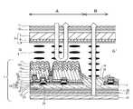
TFT基板1の反射表示領域Aにあっては、ガラス等の透明基材からなる透明絶縁基板12上に、画素2に表示信号を供給するためのスイッチング素子であるTFT13と、詳細を後述する何層かの絶縁膜を介してTFT13上に形成される反射凹凸形成層14と、この反射凹凸形成層14上に形成される平坦化層15aと、ITO膜16aを介して平坦化層15上に形成される反射電極17とを備えている。反射凹凸形成層14は、反射電極17に凹凸を形成して光の拡散性を持たせ、良好な画質を得るための層である。平坦化層15aは、反射凹凸形成層14による凹凸を緩和して、反射表示品質のさらなる向上を図るために設けられる層である。
【0033】
なお、図1に示す液晶表示装置では、ITO膜16aと後述する透明電極16とは同時に形成され一体化したものであるが、本明細書では説明を容易とするために、反射表示領域Aに存在するものをITO膜16a、透過表示領域Bに存在するものを透明電極16と呼び分けることとする。また、平坦化層15aと後述する絶縁平坦化層15とは同時に形成され一体化したものであるが、同様の理由から、反射表示領域Aに存在するものを平坦化層15a、透過表示領域Bに存在するものを絶縁平坦化層15と呼び分けることとする。
【0034】
この図2に示すTFT13は、いわゆるボトムゲート構造であり、透明絶縁基板12上に形成されたゲート電極18と、ゲート電極18の上面に重ねられた例えば窒化シリコン膜19a及び酸化シリコン膜19bの積層膜からなるゲート絶縁膜19と、ゲート絶縁膜19上に重ねられた半導体薄膜20とを有し、半導体薄膜20の両脇がN+拡散領域とされている。ゲート電極18は、ゲート線3の一部を延在させたものであり、モリブデン(Mo)、タンタル(Ta)等の金属又は合金がスパッタリング等の方法によって成膜されてなる。
【0035】
半導体薄膜20の一方のN+拡散領域には、第1の層間絶縁膜21及び第2の層間絶縁膜22に形成されたコンタクトホールを介してソース電極28が接続される。ソース電極28には信号線4が接続され、データ信号が入力される。また、半導体薄膜20の他方のN+拡散領域には、第1の層間絶縁膜21及び第2の層間絶縁膜22に形成されたコンタクトホールを介してドレイン電極29が接続される。ドレイン電極29は、接続電極と接続され、さらにコンタクト部を介して画素2と電気的に接続される。接続電極は、ゲート絶縁膜19を介してCs線23との間に補助容量Cを形成している。半導体薄膜20は、例えばCVD法等によって得られる低温ポリシリコンからなる薄膜であり、ゲート絶縁膜19を介してゲート電極18と整合する位置に形成される。
【0036】
半導体薄膜20の第1の層間絶縁膜21及び第2の層間絶縁膜22を介した直上には、ストッパ24が設けられる。このストッパ24は、ゲート電極18と整合する位置に形成された半導体薄膜20を保護するものである。
【0037】
本発明のTFT基板1の透過表示領域Bにおいては、反射表示領域Aを構成する膜のうち平坦化層15a及びITO膜16aの一部が、透明絶縁基板12上に延在されて絶縁平坦化層15及び透明電極16として形成されている。なお、反射表示領域Aを構成するゲート絶縁膜19、第1の層間絶縁膜21、第2の層間絶縁膜22、反射凹凸形成層14、及び反射電極17は、透過表示領域Bにおいては除去されている。
【0038】
また、TFT基板1のTFT13等が形成された反対側の面、すなわち、内部光源たるバックライト25が配される側の面には、カラーフィルタ基板5と同様に、λ/4層26と偏光板27とがこの順に配設される。
【0039】
上述したTFT基板1及びカラーフィルタ基板5に挟持される液晶層6は、正の誘電異方性を有するネマチック液晶分子であり、電圧無印加時に液晶分子が基板に対して水平配向し、電圧印加時に液晶分子が基板に対して垂直配向する。印加する電圧に応じて液晶の複屈折を制御し、明るさを制御することができる。なお、液晶層6は上述の構成に限定されず、電圧印加時に液晶分子が基板に対して水平配向し、電圧無印加時に液晶分子が基板に対して垂直配向するような構成であってもよい。
【0040】
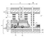
次に、本発明の液晶表示装置の図1中のD−D'線における断面構造、すなわち、透過表示領域Bの略中央を通り、且つゲート線3に平行な断面構造について図3、及び図3中の信号線4付近を拡大した断面構造について図4を参照しながら説明する。
【0041】
図3及び図4に示すように、この液晶表示装置においては、信号線4を絶縁平坦化層15で被覆することで、信号線4と透明電極16とをオーバーラップ(部分的に重なり合う)させた状態で配置した場合でも、信号線4と透明電極16とを確実に絶縁する。これにより、従来は困難であった信号線4近傍における透過表示領域Bの拡大が期待される。
【0042】
そしてこの液晶表示装置においては、信号線4を被覆し、且つ透過表示領域Bにおける透明絶縁基板12の略全面にわたって絶縁平坦化層15が形成され、この上に透明電極16が形成されるので、平坦性の高い透明電極16が得られる。このため、信号線4とオーバーラップさせた状態で透明電極16を形成させる場合でも、透明電極16の下地の平坦性が確保されるので、透明電極16の段差による黒表示時の光漏れがない。
【0043】
また、透明電極16の平坦性を確保して黒表示時の光漏れを防止しているので、従来カラーフィルタ基板5側に設けられていたブラックマトリクスが、図3に示すように不要となる。この結果、ブラックマトリクスを設けることで犠牲となっていた透過率の低下がなくなり、透過率が飛躍的に向上するので透過表示時の表示品質をさらに高めることができる。
【0044】
勿論、カラーフィルタ基板5にブラックマトリクスを設けて遮光する従来の光り漏れを防止する手法と本発明の絶縁平坦化層15により透明電極16の平坦性を向上する手法とを組み合わせるとともに、ブラックマトリクスで遮光する領域を従来に比べて縮小させることにより透過率を向上させることも可能である。しかしながらこの場合、ブラックマトリクスの最小線幅、カラーフィルタ基板5とTFT基板1とのあわせ精度、プロセスマージン等を考慮すると、結局ブラックマトリクスで遮光する領域の拡大を招き、透過率の向上効果が不十分となるおそれがある。
【0045】
これらの効果は、図5に示すように、信号線4と絶縁平坦化層15との間に例えば反射凹凸形成層14が延在されて形成された場合であっても同様に得ることができる。
【0046】
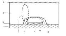
仮に、図6に示すように、信号線4と透明電極16との絶縁のみを目的として信号線4近傍にのみ絶縁平坦化層15を形成し、透明電極16の主な部分が透明絶縁基板12上に直接形成された場合には、段差部に対応する領域Eにおいて液晶配向の乱れや、セルギャップの不足による位相差のずれ等が発生し、黒表示時の光漏れを引き起こす。この結果、液晶表示装置のコントラストの低下を招いてしまう。例えば図7に示すように、信号線4と絶縁平坦化層15との間に例えば反射凹凸形成層14が延在されて形成された場合には、段差がさらに激しくなるため、コントラストの低下は著しいものとなる。
【0047】
以上のように、本発明の液晶表示装置は、透明電極16の下地を絶縁平坦化層15により平坦とするので黒表示時の光漏れがない高コントラストな画像表示を達成するとともに、信号線4の形状が平坦化されるので信号線4と透明電極16とをオーバーラップさせることが可能となり、透過表示領域Bを拡大して高い透過率を確保できる。また、従来黒表示時の光漏れを遮光するために設けられていたブラックマトリクスが不要となるため、さらなる透過率の向上が図られる。したがって、本発明によれば、高いコントラストを確保しつつ、透過表示領域Bの開口率を向上させた透過表示重視型の液晶表示装置を実現することができる。
【0048】
なお、透過表示領域Bに隣接する信号線4は、図4及び図5に示すように透明絶縁基板12上、すなわち、透過表示領域Bにおける透明電極16と同じ面上に直接形成されることが好ましい。この構造とすることにより、信号線4領域と透過表示領域Bとの段差を最小とし、且つ製造プロセスを容易とすることができる。
【0049】
透過表示領域Bの絶縁平坦化層15は、反射表示領域Aの少なくとも一部、具体的には平坦化層15a、反射凹凸形成層14の少なくともの一部であることで、製造工程を増やすことなく形成することができる。絶縁平坦化層15としては、反射表示領域Aを構成する平坦化層15aをそのまま延在させたものであることが特に好ましい。製造工程数の増加をいとわない場合には、透過表示領域Bの絶縁平坦化層15を、反射表示領域Aの一部として形成せずに独立して設けてもかまわない。
【0050】
絶縁平坦化層15は、例えばウェットプロセス、より具体的には凹凸の埋め込み性に優れるスピンコート法等により感光性材料を塗布し、フォトリソグラフィ、具体的には反射表示領域Aと透過表示領域Bとで露光条件を変えて透過表示領域Bにおける膜厚を薄くすることにより形成される。これにより、製造工程を増やすことなく絶縁平坦化層15を形成できる。
【0051】
絶縁平坦化層15を構成する材料は、透過表示領域Bを構成することから透明であることが重要であり、具体的にはアクリル系樹脂、ノボラック系樹脂、ポリイミド、シロキサン系ポリマー、シリコン系ポリマー等の樹脂材料が挙げられ、中でもアクリル系樹脂が好ましい。また、工程数を増加させずに透過表示領域Bの絶縁平坦化層15を形成するためには、フォトリソグラフィに使用可能な感光性材料を用いることが好ましい。また、高度な平坦性を得るためには、スピンコート等の塗布により絶縁平坦化層15を形成可能な材料を用いることが重要となる。このような材料としては、上述した樹脂材料のような有機材料や、例えばSiO2を主成分とするSOG(Spin On Glass)材料等が挙げられる。
【0052】
ところで、絶縁平坦化層15によって信号線4の段差の緩和が図られるが、図4及び図5に示すように、絶縁平坦化層15の表面には信号線4の形状が若干現れることがあるので、絶縁平坦化層15は完全に平坦な表面とされなくても良い。但しあまり凹凸が大きいと透明電極16の平坦性が損なわれるため、例えば透過表示領域Bにおけるセルギャップをd(T)とすると、透過表示領域Bの透明電極16の表面の凹凸は、d(T)×0.2以下の範囲に収まることが好ましく、d(T)×0.07以下の範囲であることがより好ましい。
【0053】
また、図4及び図5に示すように、透過表示領域Bにおける透明絶縁基板12に対応する位置から信号線4に対応する位置にかけての絶縁平坦化層15の立ち上がり角度θが20°以下であることで、黒表示時の光漏れ抑制効果を確実に得られる。
【0054】
凹凸形状の原因となる信号線4の高さは、通常0.1μm〜1μm程度で形成される。透過表示領域Bに形成される絶縁平坦化層15の凹凸は、元の凹凸に対して0.5倍以上が好ましい。
【0055】
ところで、本発明の液晶表示装置が良好な画像表示を実現するためには、反射表示領域Aと透過表示領域Bとのセルギャップが所定の関係を満足する必要がある。
【0056】
そこで次に、図2に示すような反射表示領域Aと透過表示領域Bとで異なるセルギャップを示す、いわゆるマルチギャップの液晶表示装置における、反射表示領域A及び透過表示領域Bのそれぞれの最適なセルギャップについて説明する。
【0057】
透過表示領域Bから表示される光は、バックライト25から出射された後、液晶層6を1回通過してくる。これに対して、反射表示領域Aから表示される光は、表示面から入射した周囲光が反射電極17で跳ね返されて液晶層6を往復するので、液晶層6を2回通過してくる。
【0058】
いま、液晶表示装置の透過表示領域Bの光路長、すなわち透過表示領域Bのセルギャップをd(T)とし、反射表示領域Aのセルギャップをd(R)としたときに、d(T)をd(R)の約2倍とすることが好ましい。透過表示領域Bのセルギャップd(T)の最適範囲は、以下の式(1)の範囲内である。
【0059】
1.4×d(R)<d(T)<2.3×d(R)...式(1)
【0060】
d(T)が上記範囲より小さくなると、透過率が低くなり、バックライト25の光利用効率が極端に悪くなる。また、d(T)が上記範囲より大きくなると、反射表示領域Aと透過表示領域Bとの階調の電圧依存性が崩れ、反射表示領域Aと透過表示領域Bとで異なる画を表示するおそれがある。
【0061】
反射表示領域Aのセルギャップは、以下のように決まる。液晶層6に最低電圧を印加したとき(通常は無電圧印加時)の液晶層6の位相差をαとし、液晶層6に最大電圧を印加したときの液晶層6の位相差をβとしたとき、αとβとの差が約λ/4となるように設計することが好ましい。液晶層6がツイスト配向する場合も、同様にαとβとの差が見かけ上λ/4程度になることが好ましい。ここでλは光の波長であり、通常の液晶表示装置の場合、視感度が高い約550nmの波長の光を中心として設計される。
【0062】
ところで、液晶層6の位相差は、液晶の屈折率異方性Δn及びそのセルギャップd、並びに液晶の配向で決まる。
【0063】
このとき、液晶の屈折率異方性Δnはある程度の範囲に規制されるため、最適なセルギャップdもある程度の範囲内に規制される。また、セルギャップdが大きすぎると液晶の応答速度が極端に遅くなり、逆に狭くなりすぎるとセルギャップの制御が困難となる。
【0064】
以上のことを考慮すると、反射表示領域Aのセルギャップd(R)は、以下の式(2)を満たすことが好ましい。
【0065】
1.5μm<d(R)<3.5μm...式(2)
【0066】
そして、反射表示領域Aと透過表示領域Bとの段差は、以上の式(1)及び式(2)の条件を満足することが好ましい。すなわち、式(1)の条件から、1.4×d(R)<d(T)<2.3×d(R)であり、式(1)及び式(2)の条件より、透過表示領域Bのセルギャップd(T)は、2.1μm<d(T)<8.05μmの範囲内であることが好ましいといえる。
【0067】
また、絶縁平坦化層15の膜厚は、厚すぎると反射表示領域Aと透過表示領域Bとで必要な段差を埋めてしまうので、TFT基板1の反射表示領域Aと透過表示領域Bとの段差の40%以下であることが好ましい。上述したセルギャップの条件を考慮すると、絶縁平坦化層15の膜厚は0.2μm〜1μmの範囲内であることが好ましい。
【0068】
図2に示す構成の液晶表示装置では、TFT基板1における反射表示領域Aの高さを通常よりも高くすることにより、反射表示領域Aと透過表示領域Bとのセルギャップを上述したように最適化している。具体的には、反射電極17、反射凹凸形成層14等の膜厚を厚くすることにより反射表示領域Aにおけるセルギャップを薄くし、反射表示領域Aの光路長を調整する。
【0069】
ところで、反射表示領域A及び透過表示領域Bのセルギャップの最適化は、上述の方法に限定されず、図8及び図9に示すように、透過表示領域Bに対応する透明絶縁基板12の表面を除去して凹ませ、透過表示領域Bのセルギャップを厚くする方法によっても実現可能である。この方法は、透過表示領域Bに延在された絶縁平坦化層15の厚みを透明絶縁基板12の凹みでキャンセルし、反射表示領域Aと透過表示領域Bとで必要な段差を確保することが容易であるため好ましい手法である。透明絶縁基板12に設けられる凹みは、例えばゲート絶縁膜19をドライエッチング等でパターニング除去する際に透明絶縁基板12を過剰にエッチングすることで形成される。
【0070】
なお、透明絶縁基板12の凹みは図8中、一点鎖線Hと一点鎖線Iとで挟まれる領域に設けられ、透過表示領域B内で透明絶縁基板12が凹まない部分が生じる。ゲート線3上にはゲート絶縁膜19を残さなければならないので、ゲート線3近傍の透過表示領域Bにおいては、透明絶縁基板12がエッチングされない。これに対して、信号線4下の透明絶縁基板12はエッチングにより表面が除去される。
【0071】
また、これらの方法を組み合わせて反射表示領域A及び透過表示領域Bのセルギャップを最適化することも勿論可能である。
【0072】
なお、上述の説明では、透過表示領域Bにおける信号線4の凸形状を被覆・平坦化する場合について述べたが、図2に示すように透過表示領域Bにおけるゲート線3の凸形状を被覆・平坦化する場合についても、信号線4と同様のことがいえる。
【0073】
また、上述の説明では、画素2を反射表示領域Aと透過表示領域Bとで2分割する構成について図1に例示したが、本発明はこの構成に限定されることなく、例えば図10に示すように、透過表示領域Bとゲート線3との間に反射表示領域Aが介在し、画素2を3分割する構成であってもかまわない。また、画素2において反射表示領域Aに周囲を囲まれた状態で透過表示領域Bが設けられるような、従来公知の反射透過併用型液晶表示装置に本発明を適用することも勿論可能である。
【0074】
また、本発明は上述の記載に限定されることはなく、本発明の要旨を逸脱しない範囲において適宜変更可能である。
【0075】
【発明の効果】
以上の説明からも明らかなように、本発明によれば、黒表示時の光漏れを防止して高コントラストを実現するとともに、透過表示領域を拡大して高透過率を得ることが可能な反射透過併用型の液晶表示装置を提供することができる。
【図面の簡単な説明】
【図1】本発明を適用した反射透過併用型の液晶表示装置の一例であり、TFT基板の平面図である。
【図2】図1中C−C'線における断面図である。
【図3】図1中D−D'線における断面図である。
【図4】図3中、信号線付近を拡大した断面図の一例である。
【図5】図3中、信号線付近を拡大した断面図の他の例である。
【図6】透過表示領域が平坦化されない従来の液晶表示装置であり、信号線付近の断面図である。
【図7】透過表示領域が平坦化されない従来の液晶表示装置の他の例であり、信号線付近の断面図である。
【図8】透過表示領域に対応する透明絶縁基板の表面を掘り下げたTFT基板の平面図である。
【図9】図8中G−G'線における断面図である。
【図10】本発明を適用した反射透過併用型の液晶表示装置の他の例であり、TFT基板の平面図である。
【図11】従来の液晶表示装置のTFT基板の要部平面図である。
【図12】図11に示すTFT基板を備える従来の液晶表示装置の断面図であり、図11中J−J'断面図である。
【図13】図11中K−K'断面であり、透過表示領域における透明電極と信号線との位置関係を説明するための概略断面図である。
【図14】図11中K−K'断面の他の例であり、透過表示領域が平坦化されない場合を説明するための、信号線付近の概略断面図である。
【符号の説明】
1 TFT基板
2 画素
3 ゲート線
4 信号線
5 カラーフィルタ基板
6 液晶層
7 透明絶縁基板
8 カラーフィルタ
9 対向電極
10 λ/4層
11 偏光板
12 透明絶縁基板
13 TFT
14 反射凹凸形成層
15 絶縁平坦化層
15a 平坦化層
16 透明電極
16a ITO膜
17 反射電極
18 ゲート電極
19 ゲート絶縁膜
20 半導体薄膜
21 第1の層間絶縁膜
22 第2の層間絶縁膜
23 Cs線
24 ストッパ
25 バックライト
26 λ/4層
27 偏光板[0001]
BACKGROUND OF THE INVENTION
The present invention relates to a liquid crystal display device, and more particularly to an improvement of a reflection / transmission combined type liquid crystal display device.
[0002]
[Prior art]
Liquid crystal display devices are widely used in notebook personal computers, display devices for car navigation, personal digital assistants (PDAs), and mobile phones, taking advantage of their thinness and low power consumption. This liquid crystal display device has an internal light source called a backlight, and a transmissive liquid crystal display device that performs display by switching on and off the light from the backlight with a liquid crystal panel, and ambient light such as sunlight. There is known a reflection type liquid crystal display device in which light is reflected by a reflecting plate or the like, and the reflected light is turned on / off by a liquid crystal panel for display.
[0003]
In the transmissive liquid crystal display device described above, the backlight accounts for 50% or more of the total power consumption of the display device, and there is a problem that the power consumption increases by providing such a backlight. In addition, the transmissive liquid crystal display device has a problem that when the surroundings are bright, the display light looks dark and visibility is lowered. On the other hand, in the reflective liquid crystal display device, there is no problem of increased power consumption because no backlight is provided, but when the surroundings are dark, there is a problem that the amount of reflected light is reduced and the visibility is extremely lowered. is there.
[0004]
In order to solve such problems of both transmissive and reflective display devices, a reflective / transmissive liquid crystal display device that realizes both transmissive display and reflective display with a single liquid crystal panel has been proposed. ing. In this reflective / transmissive liquid crystal display device, when the surroundings are bright, display by reflection of ambient light (reflection display) is performed, and when the surroundings are dark, display by backlight (transmission display) is performed. Examples of the reflection / transmission combined type liquid crystal display device are disclosed in Japanese Patent No. 2955277, Japanese Patent Application Laid-Open No. 2001-166289, and the like.
[0005]
FIG. 11 shows a planar structure of a thin film transistor (hereinafter referred to as TFT)
[0006]
The
[0007]
Further, the
[0008]
FIG. 12 shows a cross-sectional structure of the liquid crystal display device taken along line JJ ′ in FIG. This liquid crystal display device has a structure in which the above-described
[0009]
The
[0010]
A λ / 4 layer 110 and a polarizing
[0011]
In the reflective display region A of the
[0012]
The TFT 113 shown in FIG. 12 has a so-called bottom gate structure, and is a laminated film of a
[0013]
One N of the semiconductor thin film 120+ A
[0014]
A
[0015]
In the transmissive display region B of the
[0016]
Similarly to the
[0017]
FIG. 13 shows a cross section taken along the line KK ′ of the
[0018]
[Problems to be solved by the invention]
However, the reflection / transmission combined type liquid crystal display device has a problem that light leakage at the time of black display is likely to occur at a step portion between the reflection display area A and the transmission display area B in FIG. Light leakage at the time of black display is caused by a region where the liquid crystal alignment is disturbed at the stepped portion, or a cell gap is insufficient at the stepped portion and the phase difference is shifted.
[0019]
The reduction in contrast due to light leakage during black display tends to become more prominent when a structure that emphasizes transmissive display is adopted. That is, as shown in FIG. 14, when an attempt is made to expand the
[0020]
In order to prevent light leakage, as shown in FIGS. 13 and 14, a
[0021]
Therefore, the present invention has been proposed to solve such a conventional problem, and while improving the transmission display area to ensure high transmittance, it prevents light leakage during black display and improves contrast. An object of the present invention is to provide a reflective / transmissive liquid crystal display device capable of achieving the above.
[0022]
[Means for Solving the Problems]
In order to achieve the above-described object, a liquid crystal display device according to the present invention includes a transmissive display region in which a liquid crystal layer is sandwiched between a pair of substrates and a display is performed using transmitted light, and a reflective display region that is displayed using reflected light. And the one substrate isIn the reflective display region, comprising a reflective irregularity forming layer having irregularities for diffusing light, In the transmissive display region, an insulating flattening layer for flattening a step between a signal line and / or a gate line for supplying a signal to the driving element, and a transparent electrode formed on the insulating flattening layer,The insulating planarization layer is formed to extend from the reflective display region to the transmissive display region, and is formed on the reflective unevenness forming layer in the reflective display region, The insulating flattening layer is formed so as to flatten a step of the signal line and / or the gate line only in the transmissive display region of the transmissive display region and the reflective display region. The thickness of the liquid crystal layer is different between the transmissive display region and the transmissive display region.
[0023]
In the liquid crystal display device configured as described above, since the base of the transparent electrode is flattened by the insulating flattening layer, the flatness of the transparent electrode can be improved without depending on the step shape of the signal line and / or the gate line. Secure. For example, even when the transmissive display region is enlarged so as to partially overlap with the signal line and / or the gate line, no step is generated in the transparent electrode. As a result, light leakage during black display in the transmissive display area is prevented.
[0024]
DETAILED DESCRIPTION OF THE INVENTION
Hereinafter, a liquid crystal display device to which the present invention is applied will be described in detail with reference to the drawings. Note that the drawings used in the following description may show characteristic portions of the invention in an enlarged manner for ease of explanation, and the dimensional ratios of the respective constituent elements are not always the same.
[0025]
FIG. 1 shows a planar structure of a TFT substrate 1 in a reflection / transmission combined type liquid crystal display device to which the present invention is applied. A plurality of
[0026]
Further, the TFT substrate 1 is provided with a storage capacitor wiring (not shown) (hereinafter referred to as Cs line) made of a metal film parallel to the
[0027]
The
[0028]
Next, a cross-sectional structure taken along line CC ′ in FIG. 1 of the liquid crystal display device of the present invention, that is, a cross-sectional structure passing through the approximate center of the
[0029]
The
[0030]
In the reflection / transmission combined type liquid crystal display device, display is performed by light from a backlight that passes through the color filter 8 only once in transmissive display. On the other hand, in reflective display, display is performed with ambient light that passes through the color filter 8 twice, when it is incident from the outside and when it is reflected and emitted to the outside. As described above, in the reflective display, since the light passes through the color filter 8 more than in the transmissive display, the amount of light attenuation becomes extremely larger than that in the transmissive display, which causes a decrease in reflectance. Yes. For this reason, reflection is performed by a method such as providing an opening in the color filter 8 corresponding to the reflective display area A, forming a thin film thickness, or changing the pigment dispersed in the resin to a material suitable for reflective display. It is preferable to reduce the amount of light attenuation in the display area A and increase the reflectance. In particular, a method of providing an opening in the color filter 8 corresponding to the reflective display area A is preferable. According to this method, the amount of light passing therethrough can be adjusted depending on the size of the opening, so that the color filter 8 corresponding to the reflective display area A and the color filter 8 corresponding to the transmissive display area B have the same conditions, specifically Can be easily formed in the same process with the same film thickness and the same material, improving the reflectance in the reflective display, and further improving the luminance and color reproducibility without increasing the number of manufacturing processes, and visually recognizing the reflective display Can be improved.
[0031]
A λ / 4 layer 10 and a
[0032]
In the reflective display region A of the TFT substrate 1, a
[0033]
In the liquid crystal display device shown in FIG. 1, the
[0034]
The
[0035]
One N of the semiconductor thin film 20+ A
[0036]
A
[0037]
In the transmissive display region B of the TFT substrate 1 of the present invention, a part of the
[0038]
Similarly to the
[0039]
The
[0040]
Next, a cross-sectional structure taken along line DD ′ in FIG. 1 of the liquid crystal display device of the present invention, that is, a cross-sectional structure passing through the approximate center of the transmissive display region B and parallel to the
[0041]
As shown in FIGS. 3 and 4, in this liquid crystal display device, the
[0042]
In this liquid crystal display device, since the insulating
[0043]
Further, since the flatness of the
[0044]
Of course, the conventional method of preventing light leakage by providing a black matrix on the
[0045]
As shown in FIG. 5, these effects can be similarly obtained even when, for example, the reflection
[0046]
As shown in FIG. 6, an insulating
[0047]
As described above, in the liquid crystal display device of the present invention, the base of the
[0048]
The
[0049]
The insulating
[0050]
The insulating
[0051]
Since the material constituting the insulating
[0052]
By the way, although the step of the
[0053]
4 and 5, the rising angle θ of the insulating
[0054]
The height of the
[0055]
By the way, in order for the liquid crystal display device of the present invention to realize a good image display, the cell gap between the reflective display area A and the transmissive display area B needs to satisfy a predetermined relationship.
[0056]
Therefore, next, in the so-called multi-gap liquid crystal display device that shows different cell gaps in the reflective display area A and the transmissive display area B as shown in FIG. The cell gap will be described.
[0057]
The light displayed from the transmissive display area B is emitted from the
[0058]
Now, when the optical path length of the transmissive display area B of the liquid crystal display device, that is, the cell gap of the transmissive display area B is d (T) and the cell gap of the reflective display area A is d (R), d (T). Is preferably about twice the d (R). The optimum range of the cell gap d (T) in the transmissive display area B is within the range of the following formula (1).
[0059]
1.4 * d (R) <d (T) <2.3 * d (R) ... Formula (1)
[0060]
When d (T) is smaller than the above range, the transmittance is lowered, and the light utilization efficiency of the
[0061]
The cell gap of the reflective display area A is determined as follows. The phase difference of the
[0062]
By the way, the phase difference of the
[0063]
At this time, since the refractive index anisotropy Δn of the liquid crystal is regulated to a certain range, the optimum cell gap d is also regulated to a certain range. If the cell gap d is too large, the response speed of the liquid crystal becomes extremely slow. Conversely, if the cell gap d is too narrow, it becomes difficult to control the cell gap.
[0064]
Considering the above, it is preferable that the cell gap d (R) of the reflective display region A satisfies the following formula (2).
[0065]
1.5 μm <d (R) <3.5 μm (2)
[0066]
The step between the reflective display area A and the transmissive display area B preferably satisfies the conditions of the above formulas (1) and (2). That is, from the condition of the expression (1), 1.4 × d (R) <d (T) <2.3 × d (R). From the conditions of the expressions (1) and (2), the transmissive display It can be said that the cell gap d (T) in the region B is preferably in the range of 2.1 μm <d (T) <8.05 μm.
[0067]
Further, if the thickness of the insulating
[0068]
In the liquid crystal display device having the configuration shown in FIG. 2, the cell gap between the reflective display area A and the transmissive display area B is optimized as described above by making the height of the reflective display area A on the TFT substrate 1 higher than usual. It has become. Specifically, the cell gap in the reflective display area A is reduced by increasing the film thickness of the
[0069]
Incidentally, the optimization of the cell gap between the reflective display area A and the transmissive display area B is not limited to the above-described method, and the surface of the transparent insulating
[0070]
Note that the recess of the transparent insulating
[0071]
It is of course possible to optimize the cell gap between the reflective display area A and the transmissive display area B by combining these methods.
[0072]
In the above description, the case where the convex shape of the
[0073]
In the above description, the configuration in which the
[0074]
Further, the present invention is not limited to the above description, and can be appropriately changed without departing from the gist of the present invention.
[0075]
【The invention's effect】
As is clear from the above description, according to the present invention, a reflection capable of preventing light leakage during black display and realizing a high contrast and enlarging a transmissive display area to obtain a high transmittance. A transmission-use liquid crystal display device can be provided.
[Brief description of the drawings]
FIG. 1 is a plan view of a TFT substrate as an example of a reflection / transmission combined use type liquid crystal display device to which the present invention is applied.
FIG. 2 is a cross-sectional view taken along the line CC ′ in FIG.
FIG. 3 is a cross-sectional view taken along the line DD ′ in FIG.
FIG. 4 is an example of an enlarged cross-sectional view of the vicinity of a signal line in FIG.
FIG. 5 is another example of a cross-sectional view in which the vicinity of the signal line in FIG. 3 is enlarged.
FIG. 6 is a cross-sectional view of the vicinity of a signal line, which is a conventional liquid crystal display device in which a transmissive display region is not flattened.
FIG. 7 is another example of a conventional liquid crystal display device in which a transmissive display region is not flattened, and is a cross-sectional view in the vicinity of a signal line.
FIG. 8 is a plan view of a TFT substrate in which the surface of the transparent insulating substrate corresponding to the transmissive display region is dug down.
FIG. 9 is a cross-sectional view taken along the line GG ′ in FIG.
FIG. 10 is a plan view of a TFT substrate as another example of a reflection / transmission combined type liquid crystal display device to which the present invention is applied.
FIG. 11 is a plan view of an essential part of a TFT substrate of a conventional liquid crystal display device.
12 is a cross-sectional view of a conventional liquid crystal display device including the TFT substrate shown in FIG. 11, and is a cross-sectional view taken along line JJ ′ in FIG.
13 is a cross-sectional view taken along the line KK ′ in FIG. 11 for explaining the positional relationship between the transparent electrode and the signal line in the transmissive display region.
FIG. 14 is another example of a cross section taken along the line KK ′ in FIG. 11, and is a schematic cross sectional view in the vicinity of a signal line for explaining a case where a transmissive display region is not flattened.
[Explanation of symbols]
1 TFT substrate
2 pixels
3 Gate line
4 signal lines
5 Color filter substrate
6 Liquid crystal layer
7 Transparent insulation substrate
8 Color filter
9 Counter electrode
10 λ / 4 layers
11 Polarizing plate
12 Transparent insulating substrate
13 TFT
14 Reflective unevenness forming layer
15 Insulating planarization layer
15a planarization layer
16 Transparent electrode
16a ITO film
17 Reflective electrode
18 Gate electrode
19 Gate insulation film
20 Semiconductor thin film
21 First interlayer insulating film
22 Second interlayer insulating film
23 Cs line
24 Stopper
25 Backlight
26 λ / 4 layers
27 Polarizing plate
Claims (13)
Translated fromJapanese上記一方の基板は、上記反射表示領域において、光を拡散させる凹凸を有する反射凹凸形成層を備え、上記透過表示領域において、駆動素子に信号を供給するための信号線及び/又はゲート線の段差を平坦化する絶縁平坦化層と、上記絶縁平坦化層上に形成された透明電極とを備え、
上記絶縁平坦化層は、上記反射表示領域から上記透過表示領域に延在して形成され、上記反射表示領域において、上記反射凹凸形成層の上に形成されており、
上記絶縁平坦化層は、上記透過表示領域と上記反射表示領域とのうちの上記透過表示領域のみにおいて、前記信号線及び/又はゲート線の段差を平坦化するように形成され、
上記反射表示領域と上記透過表示領域とで液晶層の厚みが異なることを特徴とする液晶表示装置。A liquid crystal layer is sandwiched between a pair of substrates, and includes a transmissive display region that performs display using transmitted light, and a reflective display region that performs display using reflected light.
The one substrate includesa reflective unevenness forming layer having unevenness for diffusing light in the reflective display region, and a step of a signal line and / or a gate line for supplying a signal to the driving element in the transmissive display region. An insulating flattening layer for flattening, and a transparent electrode formed on the insulating flattening layer,
The insulating planarization layer is formed to extend from the reflective display region to the transmissive display region, and is formed on the reflective unevenness forming layer in the reflective display region,
The insulating flattening layer is formed so as to flatten a step between the signal line and / or the gate line only in the transmissive display region of the transmissive display region and the reflective display region.
A liquid crystal display device, wherein the reflective display region and the transmissive display region have different liquid crystal layer thicknesses.
1.4×d(R)<d(T)<2.3×d(R)When the thickness of the liquid crystal layer in the transmissive display region is d (T) and the thickness of the liquid crystal layer in the reflective display region is d (R), the d (T) and d (R) are as follows: 2. The liquid crystal display device according to claim 1, wherein the relationship is satisfied.
1.4 × d (R) <d (T) <2.3 × d (R)
1.5μm<d(R)<3.5μmThe liquid crystal display device according to claim 1, wherein the thickness d (T) of the liquid crystal layer in the transmissive display region satisfies the following relationship.
1.5 μm <d (R) <3.5 μm
Priority Applications (5)
| Application Number | Priority Date | Filing Date | Title |
|---|---|---|---|
| JP2002175512AJP4135407B2 (en) | 2002-06-17 | 2002-06-17 | Liquid crystal display |
| US10/463,715US20040041957A1 (en) | 2002-06-17 | 2003-06-16 | Liquid crystal display |
| TW092116388ATWI252343B (en) | 2002-06-17 | 2003-06-17 | Liquid crystal display |
| CNB031526829ACN1310074C (en) | 2002-06-17 | 2003-06-17 | Lcd |
| KR1020030039054AKR101016502B1 (en) | 2002-06-17 | 2003-06-17 | Liquid crystal display |
Applications Claiming Priority (1)
| Application Number | Priority Date | Filing Date | Title |
|---|---|---|---|
| JP2002175512AJP4135407B2 (en) | 2002-06-17 | 2002-06-17 | Liquid crystal display |
Related Child Applications (1)
| Application Number | Title | Priority Date | Filing Date |
|---|---|---|---|
| JP2008105048ADivisionJP4793401B2 (en) | 2008-04-14 | 2008-04-14 | Manufacturing method of liquid crystal display device |
Publications (2)
| Publication Number | Publication Date |
|---|---|
| JP2004020907A JP2004020907A (en) | 2004-01-22 |
| JP4135407B2true JP4135407B2 (en) | 2008-08-20 |
Family
ID=31174135
Family Applications (1)
| Application Number | Title | Priority Date | Filing Date |
|---|---|---|---|
| JP2002175512AExpired - Fee RelatedJP4135407B2 (en) | 2002-06-17 | 2002-06-17 | Liquid crystal display |
Country Status (5)
| Country | Link |
|---|---|
| US (1) | US20040041957A1 (en) |
| JP (1) | JP4135407B2 (en) |
| KR (1) | KR101016502B1 (en) |
| CN (1) | CN1310074C (en) |
| TW (1) | TWI252343B (en) |
Families Citing this family (16)
| Publication number | Priority date | Publication date | Assignee | Title |
|---|---|---|---|---|
| KR100931681B1 (en)* | 2003-04-08 | 2009-12-14 | 삼성전자주식회사 | Array substrate and liquid crystal display device having same |
| JP2005031662A (en)* | 2003-07-09 | 2005-02-03 | Samsung Electronics Co Ltd | Array substrate, method of manufacturing the same, and liquid crystal display device having the same |
| JP4095606B2 (en) | 2004-01-28 | 2008-06-04 | セイコーエプソン株式会社 | Liquid crystal display device and electronic device |
| JP2005331675A (en)* | 2004-05-19 | 2005-12-02 | Sony Corp | Liquid crystal display and method for manufacturing the liquid crystal display |
| JP3953059B2 (en) | 2004-09-01 | 2007-08-01 | セイコーエプソン株式会社 | Liquid crystal display device and electronic device |
| JP4158763B2 (en)* | 2004-12-01 | 2008-10-01 | セイコーエプソン株式会社 | Liquid crystal display device, method for manufacturing liquid crystal display device, and electronic apparatus |
| JP4082418B2 (en)* | 2005-03-04 | 2008-04-30 | エプソンイメージングデバイス株式会社 | Liquid crystal device and electronic device |
| KR20060118153A (en)* | 2005-05-16 | 2006-11-23 | 삼성전자주식회사 | Semi-transmissive liquid crystal display device, display panel for this and manufacturing method thereof |
| JP2007086411A (en)* | 2005-09-22 | 2007-04-05 | Sanyo Epson Imaging Devices Corp | Liquid crystal display device, method of manufacturing liquid crystal display device and electronic equipment |
| JP2007310112A (en)* | 2006-05-18 | 2007-11-29 | Nec Lcd Technologies Ltd | Transflective liquid crystal display device and manufacturing method thereof |
| JP4924941B2 (en)* | 2006-10-13 | 2012-04-25 | Nltテクノロジー株式会社 | Optical elements, illumination optical devices, display devices, and electronic devices. |
| JP4513027B2 (en)* | 2006-12-20 | 2010-07-28 | ソニー株式会社 | Manufacturing method of display device |
| JP4793401B2 (en)* | 2008-04-14 | 2011-10-12 | ソニー株式会社 | Manufacturing method of liquid crystal display device |
| CN103488007B (en)* | 2013-09-30 | 2015-12-09 | 合肥京东方光电科技有限公司 | Array base palte and manufacture method, display device |
| JP5790978B2 (en)* | 2013-12-02 | 2015-10-07 | Nltテクノロジー株式会社 | Transflective liquid crystal display device and manufacturing method thereof |
| KR102304724B1 (en) | 2014-12-19 | 2021-09-27 | 삼성디스플레이 주식회사 | Thin film transistor substrate, display apparatus comprising the same, method for manufacturing thin film transistor substrate, and method for manufacturing display apparatus using the same |
Family Cites Families (9)
| Publication number | Priority date | Publication date | Assignee | Title |
|---|---|---|---|---|
| JP3281849B2 (en)* | 1997-10-07 | 2002-05-13 | シャープ株式会社 | Active matrix type liquid crystal display |
| US6195140B1 (en)* | 1997-07-28 | 2001-02-27 | Sharp Kabushiki Kaisha | Liquid crystal display in which at least one pixel includes both a transmissive region and a reflective region |
| JP3410663B2 (en)* | 1998-07-14 | 2003-05-26 | シャープ株式会社 | Liquid crystal display |
| JP4167335B2 (en)* | 1998-01-30 | 2008-10-15 | シャープ株式会社 | Liquid crystal display |
| IT1302704B1 (en)* | 1998-10-20 | 2000-09-29 | Lineatech S A S Di Morlacchi M | PROCEDURE FOR WATERPROOFING THE SKIN OBTAINED THROUGH THIS PROCEDURE. |
| JP4196505B2 (en)* | 1999-12-13 | 2008-12-17 | ソニー株式会社 | Display device, manufacturing method thereof, and color filter |
| US6771334B2 (en)* | 2000-09-27 | 2004-08-03 | Matsushita Electric Industrial Co., Ltd. | Transflective liquid crystal display device |
| JP4101454B2 (en)* | 2000-11-22 | 2008-06-18 | 株式会社日立製作所 | Liquid crystal display |
| US6809791B2 (en)* | 2001-02-01 | 2004-10-26 | Lg.Philips Lcd Co., Ltd. | Transflective liquid crystal display device having a color filter and method for fabricating thereof |
- 2002
- 2002-06-17JPJP2002175512Apatent/JP4135407B2/ennot_activeExpired - Fee Related
- 2003
- 2003-06-16USUS10/463,715patent/US20040041957A1/ennot_activeAbandoned
- 2003-06-17KRKR1020030039054Apatent/KR101016502B1/ennot_activeExpired - Fee Related
- 2003-06-17CNCNB031526829Apatent/CN1310074C/ennot_activeExpired - Fee Related
- 2003-06-17TWTW092116388Apatent/TWI252343B/ennot_activeIP Right Cessation
Also Published As
| Publication number | Publication date |
|---|---|
| KR101016502B1 (en) | 2011-02-24 |
| KR20040002601A (en) | 2004-01-07 |
| TWI252343B (en) | 2006-04-01 |
| US20040041957A1 (en) | 2004-03-04 |
| CN1310074C (en) | 2007-04-11 |
| TW200424603A (en) | 2004-11-16 |
| JP2004020907A (en) | 2004-01-22 |
| CN1480769A (en) | 2004-03-10 |
Similar Documents
| Publication | Publication Date | Title |
|---|---|---|
| US8259271B2 (en) | Color filter substrate and liquid crystal display panel including the same | |
| KR100728506B1 (en) | Liquid crystal device and electronic device | |
| CN100406989C (en) | Transflective liquid crystal display and manufacturing method thereof | |
| US6879359B1 (en) | Reflection type liquid crystal display provided with reflective layer, coplanar gate electrode, color filter layer and transparent pixel electrode and manufacture method thereof | |
| JP4814776B2 (en) | Transflective liquid crystal display device | |
| US7667800B2 (en) | Liquid crystal display device and method of fabricating the same | |
| JP5252334B2 (en) | Transflective liquid crystal display device | |
| JP4135407B2 (en) | Liquid crystal display | |
| US8558975B2 (en) | Liquid crystal display device and method of fabricating the same | |
| JP4638462B2 (en) | Liquid crystal display device | |
| JP3763285B2 (en) | Liquid crystal display | |
| JP3726569B2 (en) | Transflective and reflective liquid crystal devices and electronic equipment using them | |
| JP4793401B2 (en) | Manufacturing method of liquid crystal display device | |
| JP2004233959A (en) | Liquid crystal display | |
| JP4511248B2 (en) | Liquid crystal display | |
| JP2010128123A (en) | Liquid crystal display device | |
| JP2009122601A (en) | Manufacturing method of liquid crystal device | |
| JP2001066619A (en) | Liquid crystal devices and electronic equipment |
Legal Events
| Date | Code | Title | Description |
|---|---|---|---|
| A621 | Written request for application examination | Free format text:JAPANESE INTERMEDIATE CODE: A621 Effective date:20040422 | |
| RD03 | Notification of appointment of power of attorney | Free format text:JAPANESE INTERMEDIATE CODE: A7423 Effective date:20050527 | |
| RD04 | Notification of resignation of power of attorney | Free format text:JAPANESE INTERMEDIATE CODE: A7424 Effective date:20050527 | |
| A977 | Report on retrieval | Free format text:JAPANESE INTERMEDIATE CODE: A971007 Effective date:20060403 | |
| A131 | Notification of reasons for refusal | Free format text:JAPANESE INTERMEDIATE CODE: A131 Effective date:20070116 | |
| A521 | Written amendment | Free format text:JAPANESE INTERMEDIATE CODE: A523 Effective date:20070319 | |
| A131 | Notification of reasons for refusal | Free format text:JAPANESE INTERMEDIATE CODE: A131 Effective date:20070807 | |
| A521 | Written amendment | Free format text:JAPANESE INTERMEDIATE CODE: A523 Effective date:20071009 | |
| A02 | Decision of refusal | Free format text:JAPANESE INTERMEDIATE CODE: A02 Effective date:20080212 | |
| A521 | Written amendment | Free format text:JAPANESE INTERMEDIATE CODE: A523 Effective date:20080414 | |
| A911 | Transfer to examiner for re-examination before appeal (zenchi) | Free format text:JAPANESE INTERMEDIATE CODE: A911 Effective date:20080421 | |
| TRDD | Decision of grant or rejection written | ||
| A01 | Written decision to grant a patent or to grant a registration (utility model) | Free format text:JAPANESE INTERMEDIATE CODE: A01 Effective date:20080513 | |
| A01 | Written decision to grant a patent or to grant a registration (utility model) | Free format text:JAPANESE INTERMEDIATE CODE: A01 | |
| A61 | First payment of annual fees (during grant procedure) | Free format text:JAPANESE INTERMEDIATE CODE: A61 Effective date:20080526 | |
| R151 | Written notification of patent or utility model registration | Ref document number:4135407 Country of ref document:JP Free format text:JAPANESE INTERMEDIATE CODE: R151 | |
| FPAY | Renewal fee payment (event date is renewal date of database) | Free format text:PAYMENT UNTIL: 20110613 Year of fee payment:3 | |
| FPAY | Renewal fee payment (event date is renewal date of database) | Free format text:PAYMENT UNTIL: 20120613 Year of fee payment:4 | |
| R250 | Receipt of annual fees | Free format text:JAPANESE INTERMEDIATE CODE: R250 | |
| FPAY | Renewal fee payment (event date is renewal date of database) | Free format text:PAYMENT UNTIL: 20130613 Year of fee payment:5 | |
| R250 | Receipt of annual fees | Free format text:JAPANESE INTERMEDIATE CODE: R250 | |
| FPAY | Renewal fee payment (event date is renewal date of database) | Free format text:PAYMENT UNTIL: 20130613 Year of fee payment:5 | |
| S111 | Request for change of ownership or part of ownership | Free format text:JAPANESE INTERMEDIATE CODE: R313113 | |
| FPAY | Renewal fee payment (event date is renewal date of database) | Free format text:PAYMENT UNTIL: 20130613 Year of fee payment:5 | |
| R350 | Written notification of registration of transfer | Free format text:JAPANESE INTERMEDIATE CODE: R350 | |
| R250 | Receipt of annual fees | Free format text:JAPANESE INTERMEDIATE CODE: R250 | |
| R250 | Receipt of annual fees | Free format text:JAPANESE INTERMEDIATE CODE: R250 | |
| R250 | Receipt of annual fees | Free format text:JAPANESE INTERMEDIATE CODE: R250 | |
| R250 | Receipt of annual fees | Free format text:JAPANESE INTERMEDIATE CODE: R250 | |
| R250 | Receipt of annual fees | Free format text:JAPANESE INTERMEDIATE CODE: R250 | |
| R250 | Receipt of annual fees | Free format text:JAPANESE INTERMEDIATE CODE: R250 | |
| LAPS | Cancellation because of no payment of annual fees |