JP4132319B2 - Integrated circuit device and integration method - Google Patents
Integrated circuit device and integration methodDownload PDFInfo
- Publication number
- JP4132319B2 JP4132319B2JP35056898AJP35056898AJP4132319B2JP 4132319 B2JP4132319 B2JP 4132319B2JP 35056898 AJP35056898 AJP 35056898AJP 35056898 AJP35056898 AJP 35056898AJP 4132319 B2JP4132319 B2JP 4132319B2
- Authority
- JP
- Japan
- Prior art keywords
- data
- integrated circuit
- bus
- control
- processing devices
- Prior art date
- Legal status (The legal status is an assumption and is not a legal conclusion. Google has not performed a legal analysis and makes no representation as to the accuracy of the status listed.)
- Expired - Fee Related
Links
Images

Classifications
- G—PHYSICS
- G06—COMPUTING OR CALCULATING; COUNTING
- G06F—ELECTRIC DIGITAL DATA PROCESSING
- G06F9/00—Arrangements for program control, e.g. control units
- H—ELECTRICITY
- H04—ELECTRIC COMMUNICATION TECHNIQUE
- H04N—PICTORIAL COMMUNICATION, e.g. TELEVISION
- H04N21/00—Selective content distribution, e.g. interactive television or video on demand [VOD]
- H04N21/40—Client devices specifically adapted for the reception of or interaction with content, e.g. set-top-box [STB]; Operations thereof
- H04N21/41—Structure of client; Structure of client peripherals
- H04N21/426—Internal components of the client ; Characteristics thereof
Landscapes
- Engineering & Computer Science (AREA)
- Multimedia (AREA)
- Signal Processing (AREA)
- Theoretical Computer Science (AREA)
- Software Systems (AREA)
- Physics & Mathematics (AREA)
- General Engineering & Computer Science (AREA)
- General Physics & Mathematics (AREA)
- Bus Control (AREA)
- Two-Way Televisions, Distribution Of Moving Picture Or The Like (AREA)
- Compression Or Coding Systems Of Tv Signals (AREA)
Description
Translated fromJapanese【0001】
【発明の属する技術分野】
本発明は、集積回路及び集積化方法に関し、特に、セットトップボックス用の集積回路に関する。
【0002】
【従来の技術】
いわゆるセットトップボックス(Set Top Box)は、標準のテレビジョンセットに用いられ、このテレビジョンセットがケーブルネットワーク又は衛星リンクネットワークを介して伝送されてくるビデオ信号及び/又はオーディオ信号を受信できるようにするものである。
【0003】
セットトップボックスは、符号化及び多重化されたビデオデータ及び/又はオーディオデータからなる数多くのチャンネルを受信する。したがって、セットトップボックスは、アプリケーションに応じて、例えばデマルチプレクス機能、ビデオ復号機能、オーディオ復号機能、グラフィックオーバーレイ機能等の機能をそれぞれ有する様々な処理装置を備える。また、セットトップボックスは、これらの様々な処理装置を制御する少なくとも1つの制御装置を備える。さらに、セットトップボックスは、制御データを記憶したり、データの処理過程におけるビデオデータ及び/又はオーディオデータを記憶する様々なメモリを備える。
【0004】
図2は、従来のセットトップボックスの構成を示すブロック図である。
【0005】
製造コスト、信頼性、製造の容易性の観点から、セットトップボックスの主要な機能は、単一の集積回路に集約することが望まれる。しかしながら、セットトップボックスで新たなアプリケーションを動作させるためには、より強力なグラフィクス処理機能及びプロセッサパワーが必要であり、その一方で、セットトップボックス全体のコストを削減する必要もある。
【0006】
図2に示す各回路は、単一の集積回路に組み込むことができる。なお、各メモリは、集積回路の大きさ及びコストを考慮して集積回路の中に入れることもできる。例えばデマルチプレクサ(DEMUX)32用のメモリ32aは512kバイトであり、ビデオデコーダ33用のメモリ33aは2Mバイトであり、グラフィックオーバーレイ34用のメモリ34aは1Mバイトであり、メインプロセッサ38用のメモリ38aは2Mバイトである。
【0007】
一方、もう1つの手法として、メモリを除いた全て又は殆どの回路を集積化することもできる。しかしながら、集積度を高くするにつれて、より多くの処理装置を集積回路に組み込むことになり、各処理装置にそれぞれ対応した外部メモリをアクセスするためのピンを、より多く集積回路に設ける必要がある。近年の新しい集積回路は、その機能を高めるとともに配置面積を小さくして経済的に製造するために、余りにも多くのピンが必要とされている。
【0008】
本発明は、上述した従来の問題を解決するためになされたものであり、本発明の目的は、外部メモリに接続するためのピン数を少なくするとともに、内部に設けられた制御装置及び処理装置の処理能力を最大限に発揮させることができる集積回路及び集積化方法を提供することである。
【0009】
【課題を解決するための手段】
本発明に係る集積回路装置は、ビデオデータ及びオーディオデータからなる複数のチャンネルが符号化及び多重化された受信信号のうちの1つのチャンネルをデコードするものである。この集積回路装置は、ビデオデータとオーディオデータとを分離するデマルチプレクサ機能、分離されたビデオデータをデコードするビデオデコード機能、分離されたオーディオデータをデコードするオーディオデコード機能を含む複数の機能のうちの1つをそれぞれ有する複数の処理装置と、複数の処理装置を制御する少なくとも1つの制御装置と、少なくとも1つの制御装置が接続される制御バスと、複数の処理装置のうち少なくとも1つが接続されるデータバスと、制御バスとデータバスとを接続するブリッジ回路と、制御バス及びデータバスに接続され、外部メモリとの間でデータ転送を行う複数のメモリインタフェース回路とを備える。
【0010】
本発明に係る集積化方法は、ビデオデータ及びオーディオデータからなる複数のチャンネルが符号化及び多重化された受信信号のうちの1つのチャンネルをデコードする集積回路において、ビデオデータとオーディオデータとを分離するデマルチプレクサ機能、分離されたビデオデータをデコードするビデオデコード機能、分離されたオーディオデータをデコードするオーディオデコード機能を含む複数の機能のうちの1つをそれぞれ有する複数の処理装置と、複数の処理装置を制御する少なくとも1つの制御装置とを集積回路内に設け、少なくとも1つの制御装置が接続される制御バスと、複数の処理装置のうち少なくとも1つが接続されるデータバスと、制御バスとデータバスとを接続するブリッジ回路とを集積回路上に設け、制御バス及びデータバスに接続され、外部メモリとの間でデータ転送を行う複数のメモリインタフェース回路を集積回路上に設ける。
【0011】
かくして、本発明では、セットトップボックスの主要な機能を1つの集積回路内に組み込むことができる。バスに接続された全ての装置は、同じ外部メモリをアクセスすることにより、外部メモリをアクセスするために必要なピン数を少なくすることができる。また、1つの大容量のメモリのコストは、記憶容量が小さなメモリを組み合わせて同じ容量としたときよりも安い。
【0012】
ところで、集積回路とメモリ間のデータ伝送帯域は限られており、ある処理装置、特にビデオデコーダは、その機能を実行するためにメモリを頻繁に長い時間アクセスする必要がある。したがって、セットトップボックスの1つの処理装置が、そのような動作を行っているときには、セットトップボックスの他の機能は停止される。
【0013】
したがって、本発明に係る集積回路では、上述の複数のバスは、第1のデータバスと第2のデータバスとを含み、第1及び第2のデータバスには、複数の処理装置のうちの少なくとも2つが接続されており、第1及び第2のデータバスに接続され、それぞれ外部メモリとの間でデータ転送を行うメモリインタフェース回路を備える。
【0014】
また、本発明に係る集積化方法では、上述した複数の処理装置のうちの少なくとも2つを、集積回路上の複数のバスのうちの1つに接続し、複数の処理装置のうちの少なくとも2つを、集積回路上の複数のバスのうちの他の1つに接続する。
【0015】
このように構成することにより、処理装置のうちの1つが外部メモリを長い時間アクセスしていても、他の処理装置は、他の外部メモリを用いることができる。また、各処理装置は、両方のデータバスに接続されることにより、両方の外部メモリをアクセスすることができる。なお、このように、2つ以上の複数の外部メモリを使用するようにしても、処理装置毎に個別のメモリを備えるよりもコストを安くすることができる。
【0016】
また、2つのデータバスと2つの外部メモリの構成とすることにより、特に集中的なデータ処理に対しては、両方の外部メモリを使うようにすることができる。処理装置、特にビデオデコーダ等の処理装置は、高画質のアプリケーションに対しては両方の外部メモリを使うことができ、一方、普通のアプリケーションに対しては、ビデオデコーダが1つの外部メモリを使い、オーディオデコーダが他の外部メモリを使うようにすることができる。
【0017】
ところで、上述したような構成では、ビデオデコーダのような処理装置が、外部メモリとの間でデータ転送を行っている間は、制御装置は、外部メモリのアクセスが禁止される。しかし、複数の制御装置は、互いに通信する必要がある。例えば、制御プログラムは、ROMから読み出され、他の制御データは、メモリ又は入出力装置から読み出され、また書き込まれる。
【0018】
そこで、本発明に係る集積回路は、複数の制御装置を備え、上述した複数のバスのうちの1つは、複数の制御装置の全てが接続された制御バスとしている。
【0019】
また、全ての制御装置を、集積回路上の処理装置が接続されたバスとは異なる制御バスに接続するようにしている。
【0020】
このように構成することにより、処理装置がデータ処理を行っている間、集積回路内の制御装置は、全ての機能の実行及び/又は外部メモリとのデータ転送を行うことができる。
【0021】
また、本発明に係る集積回路では、データバスと制御バスを接続するためのブリッジ回路を、データバス毎に設けている。
【0022】
本発明は、データ処理、特に比較的にデータレートが高いビデオデータの処理において有益である。一方、制御データは通常低いデータレートで処理される。本発明を適用することにより、処理装置の動作が制御装置の低いデータレートの通信よって禁止されることなく、処理装置はその能力を最大限に発揮することができる。制御装置が、処理装置又はデータバスに接続された外部メモリと通信を行う必要があるときのみ、制御バスとデータバス間でデータの転送が行われる。この制御バスとデータバス間のデータ転送は、ブリッジ回路を介して行われる。この場合、ブリッジ回路はバッファとして機能し、制御バスとデータバスのデータレートが異なっていても、これらのバス間でデータの送受信ができる。
【0023】
また、本発明に係る集積回路は、外部メモリとの間でデータ転送を行うための制御バスに接続されたメモリインタフェース回路を備える。このようにすることにより、制御装置は、外部メモリとのデータ転送を制御バスを用いて行うことができる。
【0024】
また、本発明に係る集積回路では、各処理装置は、デマルチプレクサ、ビデオデコーダ、オーディオデコーダ、グラフィックプロセッサのいずれかを含む。
【0025】
また、本発明に係る集積回路では、制御装置は、メインプロセッサ、I2Cインタフェース回路、汎用非同期送受信回路、スマートカードインタフェース回路入出力ポート回路のいずれかを備える。
【0026】
【発明の実施の形態】
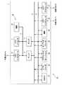
以下、本発明に係る集積回路及び集積化方法について、図面を参照しながら説明する。図1は、本発明を適用したセットトップボックス用の集積回路の構成を示すブロック図である。
【0027】
図1に示すように、この本発明を適用した集積回路1は、ブリッジ回路5,6によって分離された制御部10と、制御部10の制御下に受信信号から元のオーディオデータ及びビデオデータを再生する処理部20とを備える。
【0028】
さらに、制御部10は、図1に示すように、メインプロセッサ11と、セットトップボックスの機能に必要な各種の回路から構成される補助回路12と、この集積回路1の外部に設けられた外部メモリをアクセスするためのメモリインタフェース回路13とを備える。これらの回路は、互いに制御バス2を介して接続されている。また、制御バス2にブリッジ回路5,6が接続されている。
【0029】
補助回路12は、例えばI2Cインタフェース回路、汎用非同期送受信回路(UART)、スマートカードインタフェース回路、入出力ポート回路等を備える。メインプロセッサ11は、補助回路12を介して供給される、又は外部メモリに記憶されているプログラムを実行し、ブリッジ回路5,6を介して処理部20を制御する。
【0030】
一方、処理部20は、図1に示すように、受信信号からビデオデータとオーディオデータを分離するデマルチプレクサ(以下、DEMUXという。)21と、DEMUX21で分離されたビデオデータをデコードするビデオデコーダ22と、ビデオデコーダ22でデコードされたビデオデータにオーバーレイ処理を施すグラフィックオーバーレイ回路23と、DEMUX21で分離されたオーディオデータをデコードするオーディオデコーダ24と、その他の各種機能を有する補助回路25と、この集積回路1の外部に設けられた外部メモリをアクセスするためのメモリインタフェース回路26,27とを備える。これらの各機能をそれぞれ有する回路は、データバス3,4に接続されている。なお、メモリインタフェース回路26は、データバス3に接続されており、メモリインタフェース回路27は、データバス4に接続されている。また、データバス3,4は、それぞれブリッジ回路5,6を介して制御バス2に接続されている。
【0031】
DEMUX21は、例えばケーブルネットワーク又は衛星リンクネットワークを介して伝送されてくる複数のチャンネルが多重化された受信信号から所望のチャンネルのビデオデータとオーディオデータを分離し、ビデオデコーダ22は、DEMUX21で分離された、例えばMPEG2方式で圧縮されているビデオデータをデコードして伸長する。グラフィックオーバーレイ回路23は、ビデオデコーダ22でデコードされたビデオデータに、画像をオーバーレイする処理を施す。一方、オーディオデコーダ24は、DEMUX21で分離された、例えばMPEG2方式で圧縮されているオーディオデータをデコードして元のオーディオデータを再生する。なお、例えばビデオ会議等のデータを送信する必要がある場合には、処理部20は、ビデオエンコーダ及びオーディオエンコーダとともに、例えば非同期転送モード(ATM)、IEEE1394規格、IEEE1284規格等に準拠した適切なインタフェース回路を備える。
【0032】
上述したように、制御部10と処理部20をブリッジ回路5,6によって分離することにより、制御部10と処理部20は独立して動作することができる。すなわち、制御部10のメインプロセッサ11は、制御バス2を介して補助回路12をアクセスするとともに、制御バス2及びメモリインタフェース回路13介して、例えばROM等の外部メモリをアクセスすることができる。これにより、メインプロセッサ11は、中断されることなく、その処理コードをアクセスすることができ、その性能が処理部20の動作によって低下されることもない。また、メインプロセッサ11は、必要に応じて、ブリッジ回路5及びデータバス3、又はブリッジ回路6及びデータバス4を介して、処理部20の各回路にアクセスすることができる。さらに、メインプロセッサ11は、プログラム実行中のデータ等を、メモリインタフェース回路13に接続された外部メモリに一時的に記憶することができる。
【0033】
ところで、例えば、メモリインタフェース回路13,26,27にそれぞれ接続された各外部メモリは、メインプロセッサ11の単一のアドレス空間に割り付けられていることから、プログラマは、異なるバス間の差異を意識する必要がない。換言すると、メインプロセッサ11は、それに関する限り、特定の回路をアクセスするためには、単に、それ自身のアドレス空間に割り当てられた特定の回路のアドレスを出力すればよく、特定の回路がどのバスに接続されているかに関する特別な動作をする必要がない。
【0034】
また、ところで、上述した2つのデータバス3,4は、異なる帯域幅を有し、例えばデータバス4は、データバス3よりも広い帯域幅を有し、広い帯域幅を要求する回路、例えばビデオデコーダ22は、データバス4を介して外部メモリをアクセスし、他の回路は、データバス3を介して外部メモリをアクセスする。すなわち、高速のアクセスと低速のアクセスは、分離独立して行われる。具体的には、ビデオデコーダ22は、データバス4及びメモリインタフェース回路27を介して外部メモリとのデータ転送を行いながら、ビデオデータをデコードし、他の回路は、データバス3及びメモリインタフェース回路26を介して外部メモリをアクセスする。
【0035】
以上の説明でも明らかなように、集積された回路又は装置毎に専用のメモリを有する従来の集積回路に比して、本発明を適用した集積回路は、外部メモリと接続するためのピン数を少なくすることができる。
【0036】
なお、本発明は、上述した実施例に限定されるものではなく、例えば図1に示す回路構成は具体的な一例である。また、例えば、原理的には、各回路は、データバス3,4の両方にアクセスするが、特別な条件における動作では、この限りではなく、少なくとも1つの回路は、1つのデータのみをアクセスするように設定される。各回路によってどのバスが使用されるかは、集積回路1の設計時、及び実際に動作中に設定される。また、例えば実行しているアプリケーションに依存して、動的に、各回路が使用するバスを設定するようにしてもよい。換言すると、設定又はアプリケーションの実行中に、特定の回路は、特定の1つのバスを使うように指示される。
【0037】
また、例えばデータバス3,4にそれぞれ接続されるメモリは、別の種類のメモリとしてもよい。例えば、いわゆるEDO−DRAM(Enhanced Data Output Dynamic RAM)と、SDRAM(Synchronous Dynamic RAM)とを用いるようにしてもよい。
【0038】
【発明の効果】
本発明係る集積回路は、少なくとも1つの制御装置と、複数の処理装置と、制御装置及び処理装置のうちの少なくとも2つを互いに接続する複数のバスと、複数のバスにそれぞれ接続され、外部メモリとの間でデータ転送を行う複数のメモリインタフェース回路とを備える。これにより、従来の集積回路に比して、外部メモリと接続するためのピン数を少なくすることができる。また、内部に設けられた制御装置及び処理装置の処理能力を最大限に発揮させることができる。
【図面の簡単な説明】
【図1】 本発明を適用したセットトップボックス用の集積回路の構成を示すブロック図である。
【図2】 従来のセットトップボックスの構成を示すブロック図である。
【符号の説明】
1 集積回路、2 制御バス、3,4 データバス、5,6 ブリッジ回路、10 制御部、11 メインプロセッサ、12 補助回路、13 メモリインタフェース回路、20 処理部、21 DEMUX、22 ビデオデコーダ、23 グラフィックオーバーレイ回路、24 オーディオデコーダ、25 補助回路、26,27 メモリインタフェース回路[0001]
BACKGROUND OF THE INVENTION
The present invention relates to an integrated circuit and an integration method, and more particularly to an integrated circuit for aset top box .
[0002]
[Prior art]
A so-called Set Top Box is used for a standard television set so that the television set can receive video and / or audio signals transmitted over a cable network or satellite link network. To do.
[0003]
The set top box receives a number of channels of encoded and multiplexed video data and / or audio data. Therefore, the set-top box includes various processing devices each having functions such as a demultiplexing function, a video decoding function, an audio decoding function, and a graphic overlay function, depending on the application. The set top box also includes at least one control device that controls these various processing devices. In addition, the set top box includes various memories for storing control data and for storing video data and / or audio data in the course of processing the data.
[0004]
FIG. 2 is a block diagram showing a configuration of a conventionalset-top box .
[0005]
From the viewpoint of manufacturing cost, reliability, and ease of manufacturing, it is desired that the main functionsof the set top box areintegrated intoa singleintegrated circuit. However, in order to operate a new application on the set top box, more powerful graphics processing functions and processor power are required, while on the other hand, the cost of the entire set top box needs to be reduced.
[0006]
Each circuit shown in FIG. 2 can be incorporated into a singleintegrated circuit. Note that each memory can be included in the integrated circuit in consideration of the size and cost of the integrated circuit. For example, the
[0007]
On the other hand, as another technique, all or most of the circuits except the memory can be integrated. However, as the degree of integration increases, more processing devices are incorporated in the integrated circuit, and more pins need to be provided in the integrated circuit to access external memories corresponding to the respective processing devices. Newer integrated circuits in recent years require too many pins in order to increase their function and reduce the layout area and make them economically.
[0008]
The present invention has been made in order to solve the above-described conventional problems, and an object of the present invention is to reduce the number of pins for connecting to an external memory and to provide a control device and a processing device provided therein. It is an object to provide anintegrated circuit and an integration method capable of maximizing the processing capability.
[0009]
[Means for Solving the Problems]
The integrated circuit device according to the present invention decodes one channel of received signals in which a plurality of channels including video data and audio data are encoded and multiplexed. This integrated circuit device includes a demultiplexer function for separating video data and audio data, a video decoding function for decoding separated video data, and an audio decoding function for decoding separated audio data. A plurality of processing devices each having one,at least one control device for controlling the plurality of processing devices, a control bus to which at least one control device is connected , andat least one of the plurality of processing devices are connected. A data bus, a bridge circuit that connects the control bus and the data bus , and a plurality of memory interface circuits that are connected to thecontrol bus and the data bus and transfer data to and from an external memory.
[0010]
An integration method according to the present invention separates video data and audio data in an integrated circuit that decodes one of received signals in which a plurality of channels consisting of video data and audio data are encoded and multiplexed. A plurality of processing devices each having one of a plurality of functions including a demultiplexer function, a video decoding function for decoding the separated video data, and an audio decoding function for decoding the separated audio data, and a plurality of processes At least one control device for controlling the device is provided in the integrated circuit,a control bus to which at least one control device is connected, a data bus to which at least one of a plurality of processing devices is connected, a control bus and data It provideda bridge circuit for connecting the bus on the integrated circuit,the control bus It is connected to themicro data bus, providing a plurality of memory interface circuit for performing data transfer between the external memory on the integrated circuit.
[0011]
Thus, in the present invention, the main functions of the set top box can be incorporated in one integrated circuit. All devices connected to the bus can access the same external memory, thereby reducing the number of pins required to access the external memory. In addition, the cost of one large-capacity memory is lower than when a memory having a small storage capacity is combined into the same capacity.
[0012]
By the way, the data transmission band between the integrated circuit and the memory is limited, and a certain processing device, particularly a video decoder, needs to frequently access the memory for a long time in order to perform its function. Therefore, when one processing device of the set top box performs such an operation, other functions of the set top box are stopped.
[0013]
Therefore,an integrated circuit according to the present invention, a plurality of buses described above, includes a first data bus anda second data bus, the first and second data buses, among the plurality of processing devices Are connected tothe first and second data buses,and each has a memoryinterface circuit for transferring data to and from an external memory.
[0014]
In the integration method according to the present invention, at least two of the plurality of processing devices described above are connected to one of the plurality of buses on the integrated circuit, and at least two of the plurality of processing devices are connected. One to the other of the buses on the integrated circuit.
[0015]
With such a configuration, even if one of the processing devices accesses the external memory for a long time, another processing device can use the other external memory. Further, each processing apparatus can access both external memories by being connected to both data buses. Even when two or more external memories are used as described above, the cost can be reduced as compared with the case where each processing apparatus is provided with an individual memory.
[0016]
In addition, with the configuration of two data buses and two external memories, bothexternal memories can be used particularly for intensive data processing. Processing apparatus, in particular apparatus such as a video decoder can use both the external memory for high-quality applications, whereasin pairs in a normal application, the video decoder uses a single external memory The audio decoder can use other external memory.
[0017]
Incidentally, in the structure described above, the processing apparatus such as a video decoder, while performing data transfer with the external memory, the control device accesses the external memoryis inhibited. However, the plurality of control devices need to communicate with each other. For example, the control program is read from the ROM, and other control data is read and written from the memory or the input / output device.
[0018]
Therefore, the integrated circuit according to the present invention includes a plurality of control devices, and one of the plurality of buses described above is a control bus to which all of the plurality of control devices are connected.
[0019]
Further, all the control devices are connected to a control bus different from the bus to which the processing device on the integrated circuit is connected.
[0020]
With this configuration, the control device in the integrated circuit can execute all functions and / or transfer data to / from an external memory while the processing device performs data processing.
[0021]
In the integrated circuit according to the present invention, a bridge circuit for connecting the data bus and the control bus is provided for each data bus.
[0022]
The present invention is useful in data processing, particularly in processing video data with a relatively high data rate. On the other hand, control data is usually processed at a low data rate. By applying the present invention, the operation of the processing device is not prohibited by the low data rate communication of the control device, and the processing device can maximize its capability. Data transfer is performed between the control bus and the data bus only when the control device needs to communicate with the processing device or the external memory connected to the data bus. Data transfer between the control bus and the data bus is performed via a bridge circuit. In this case, the bridge circuit functions as a buffer, and data can be transmitted and received between these buses even if the data rates of the control bus and the data bus are different.
[0023]
An integrated circuit according to the present invention includes a memoryinterface circuit connected to a control bus for performing data transfer with an external memory. By doing so, the control device can perform data transfer with the external memory using the control bus.
[0024]
In the integrated circuit according to the present invention,each processing device includes any of a demultiplexer, a video decoder, an audio decoder, and a graphic processor.
[0025]
In the integrated circuit according to the present invention, thecontrol device includes any of a main processor, an I2C interface circuit, a general-purpose asynchronous transmission / reception circuit, and a smart card interface circuit input / output port circuit.
[0026]
DETAILED DESCRIPTION OF THE INVENTION
Hereinafter, an integrated circuit and an integration method according to the present invention will be described with reference to the drawings. FIG. 1 is a block diagram showing a configuration of an integrated circuit for a set top box to which the present invention is applied.
[0027]
As shown in FIG. 1, an integrated circuit 1 to which the present invention is applied includes a
[0028]
Further, the
[0029]
The
[0030]
On the other hand, as shown in FIG. 1, the
[0031]
For example, the
[0032]
As described above, by separating the
[0033]
By the way, for example, each external memory connected to each of the
[0034]
Meanwhile, the two data buses 3 and 4 described above have different bandwidths. For example, the data bus 4 has a wider bandwidth than the data bus 3, and a circuit that requires a wider bandwidth, such as a video. The
[0035]
As is clear from the above description, the integrated circuit to which the present invention is applied has a smaller number of pins for connecting to an external memory than a conventional integrated circuit having a dedicated memory for each integrated circuit or device. Can be reduced.
[0036]
In addition, this invention is not limited to the Example mentioned above, For example, the circuit structure shown in FIG. 1 is a specific example. Further, for example, in principle, each circuit accesses both of the data buses 3 and 4, but this is not limited to the operation in a special condition, and at least one circuit accesses only one data. Is set as follows. Which bus is used by each circuit is set when the integrated circuit 1 is designed and during actual operation. Also, for example, depending on the application being executed, the bus used by each circuit may be set dynamically. In other words, during configuration or application execution, a particular circuit is instructed to use one particular bus.
[0037]
For example, the memories connected to the data buses 3 and 4 may be different types of memories. For example, so-called EDO-DRAM (Enhanced Data Output Dynamic RAM) and SDRAM (Synchronous Dynamic RAM) may be used.
[0038]
【The invention's effect】
An integrated circuit according to the present invention includes at least one control device, a plurality of processing devices,a plurality of busesconnecting at least two of the control devicesand the processing devicesto each other, and a plurality of buses, respectively, and an external memory And a plurality of memoryinterface circuits that perform data transfer between them. Thereby, the number of pins for connecting to the external memory can be reduced as compared with the conventional integrated circuit. Further, the processing capability of the control device and the processing device provided inside can be maximized.
[Brief description of the drawings]
FIG. 1 is a block diagram showing a configuration of an integrated circuit for a set top box to which the present invention is applied.
FIG. 2 is a block diagram showing a configuration of a conventionalset-top box .
[Explanation of symbols]
DESCRIPTION OF SYMBOLS 1 Integrated circuit, 2 Control bus, 3, 4 Data bus, 5, 6 Bridge circuit, 10 Control part, 11 Main processor, 12 Auxiliary circuit, 13 Memoryinterface circuit, 20 Processing part, 21 DEMUX, 22 Video decoder, 23 Graphics Overlay circuit, 24 audio decoder, 25 auxiliary circuit, 26, 27 memoryinterface circuit
Claims (12)
Translated fromJapaneseビデオデータとオーディオデータとを分離するデマルチプレクサ機能、分離されたビデオデータをデコードするビデオデコード機能、分離されたオーディオデータをデコードするオーディオデコード機能を含む複数の機能のうちの1つをそれぞれ有する複数の処理装置と、
上記複数の処理装置を制御する少なくとも1つの制御装置と、
上記少なくとも1つの制御装置が接続される制御バスと、
上記複数の処理装置のうち少なくとも1つが接続されるデータバスと、
上記制御バスと上記データバスとを接続するブリッジ回路と、
上記制御バス及び上記データバスに接続され、外部メモリとの間でデータ転送を行う複数のメモリインタフェース回路とを備える集積回路装置。In an integrated circuit device for decoding one channel of received signals in which a plurality of channels consisting of video data and audio data are encoded and multiplexed,
A plurality of functions each including one of a plurality of functions including a demultiplexer function for separating video data and audio data, a video decoding function for decoding separated video data, and an audio decoding function for decoding separated audio data A processing device,
At least one control device for controlling the plurality of processing devices;
A control bus to which the at least one control device is connected;
A data bus to which at least one of the plurality of processing devices is connected;
A bridge circuit connecting the control bus and the data bus;
An integrated circuit device comprising: a plurality of memory interface circuits connected to thecontrol bus and the data bus and transferring data to and from an external memory.
ビデオデータとオーディオデータとを分離するデマルチプレクサ機能、分離されたビデオデータをデコードするビデオデコード機能、分離されたオーディオデータをデコードするオーディオデコード機能を含む複数の機能のうちの1つをそれぞれ有する複数の処理装置と、上記複数の処理装置を制御する少なくとも1つの制御装置とを集積回路上に設け、
上記少なくとも1つの制御装置が接続される制御バスと、上記複数の処理装置のうち少なくとも1つが接続されるデータバスと、上記制御バスと上記データバスとを接続するブリッジ回路とを上記集積回路上に設け、
上記制御バス及び上記データバスに接続され、外部メモリとの間でデータ転送を行う複数のメモリインタフェース回路を上記集積回路上に設ける集積化方法。In an integrated circuit integrated method for decoding one channel of received signals in which a plurality of channels consisting of video data and audio data are encoded and multiplexed,
A plurality of functions each including one of a plurality of functions including a demultiplexer function for separating video data and audio data, a video decoding function for decoding separated video data, and an audio decoding function for decoding separated audio data And at least one control device for controlling the plurality of processing devices on an integrated circuit,
A control bus to which the at least one control device is connected, a data bus to which at least one of the plurality of processing devices is connected, and a bridge circuit that connects the control bus and the data bus are arranged on the integrated circuit. Provided in
An integration method in which a plurality of memory interface circuits connected to thecontrol bus and the data bus and transferring data to and from an external memory are provided on the integrated circuit.
Applications Claiming Priority (2)
| Application Number | Priority Date | Filing Date | Title |
|---|---|---|---|
| GB9726048AGB2332344A (en) | 1997-12-09 | 1997-12-09 | Set top box integrated circuit |
| GB9726048.3 | 1997-12-09 |
Publications (2)
| Publication Number | Publication Date |
|---|---|
| JPH11266447A JPH11266447A (en) | 1999-09-28 |
| JP4132319B2true JP4132319B2 (en) | 2008-08-13 |
Family
ID=10823358
Family Applications (1)
| Application Number | Title | Priority Date | Filing Date |
|---|---|---|---|
| JP35056898AExpired - Fee RelatedJP4132319B2 (en) | 1997-12-09 | 1998-12-09 | Integrated circuit device and integration method |
Country Status (5)
| Country | Link |
|---|---|
| US (1) | US6363448B1 (en) |
| EP (1) | EP0923232A3 (en) |
| JP (1) | JP4132319B2 (en) |
| KR (1) | KR100685150B1 (en) |
| GB (1) | GB2332344A (en) |
Families Citing this family (6)
| Publication number | Priority date | Publication date | Assignee | Title |
|---|---|---|---|---|
| US6708283B1 (en) | 2000-04-13 | 2004-03-16 | Stratus Technologies, Bermuda Ltd. | System and method for operating a system with redundant peripheral bus controllers |
| US6735715B1 (en)* | 2000-04-13 | 2004-05-11 | Stratus Technologies Bermuda Ltd. | System and method for operating a SCSI bus with redundant SCSI adaptors |
| US6640270B1 (en)* | 2000-06-21 | 2003-10-28 | Ulan Co., Ltd. | Terminal connection box and plug |
| US7457519B2 (en)* | 2002-04-03 | 2008-11-25 | Broadcom Corporation | Set-top box integration of integrated drive electronics |
| US7130953B2 (en)* | 2003-03-05 | 2006-10-31 | Broadcom Corporation | Bus architecture techniques employing busses with different complexities |
| US7769274B2 (en)* | 2005-05-06 | 2010-08-03 | Mediatek, Inc. | Video processing and optical recording using a shared memory |
Family Cites Families (17)
| Publication number | Priority date | Publication date | Assignee | Title |
|---|---|---|---|---|
| DE3338341A1 (en)* | 1983-10-21 | 1985-05-09 | Siemens AG, 1000 Berlin und 8000 München | MULTIPLE BUS ARRANGEMENT FOR CONNECTING PROCESSORS AND STORAGE IN A MULTIPROCESSOR SYSTEM |
| KR920007920B1 (en)* | 1989-05-30 | 1992-09-19 | 재단법인 한국전자통신연구소 | Video phone system |
| US5239654A (en)* | 1989-11-17 | 1993-08-24 | Texas Instruments Incorporated | Dual mode SIMD/MIMD processor providing reuse of MIMD instruction memories as data memories when operating in SIMD mode |
| CA2062200A1 (en)* | 1991-03-15 | 1992-09-16 | Stephen C. Purcell | Decompression processor for video applications |
| SG47015A1 (en)* | 1994-02-24 | 1998-03-20 | Intel Corp | Apparatus and method for prefetching data to load buffers in a bridge between two buses in a computer |
| US5473609A (en) | 1994-05-26 | 1995-12-05 | Thomson Consumer Electronics, Inc. | Method and apparatus for processing a conditional access program guide as for a satellite TV service |
| US5548730A (en)* | 1994-09-20 | 1996-08-20 | Intel Corporation | Intelligent bus bridge for input/output subsystems in a computer system |
| US5557758A (en)* | 1994-11-30 | 1996-09-17 | International Business Machines Corporation | Bridge between two buses of a computer system that determines the location of memory or accesses from bus masters on one of the buses |
| US5606672A (en)* | 1995-01-27 | 1997-02-25 | Intel Corporation | Method and apparatus for multiplexing signals from a bus bridge to an ISA bus interface and an ATA bus interface |
| US5664152A (en)* | 1995-06-06 | 1997-09-02 | Hewlett-Packard Company | Multiple segmenting of main memory to streamline data paths in a computing system |
| US5603051A (en)* | 1995-06-06 | 1997-02-11 | Hewlett-Packard Company | Input/output processor with a local memory providing shared resources for a plurality of input/output interfaces on an I/O bus |
| DE69601599T2 (en)* | 1995-06-07 | 1999-10-14 | Ibm | Video processing unit with control of the addressing mode |
| US5754801A (en)* | 1995-11-20 | 1998-05-19 | Advanced Micro Devices, Inc. | Computer system having a multimedia bus and comprising a centralized I/O processor which performs intelligent data transfers |
| US5929849A (en)* | 1996-05-02 | 1999-07-27 | Phoenix Technologies, Ltd. | Integration of dynamic universal resource locators with television presentations |
| US5890115A (en)* | 1997-03-07 | 1999-03-30 | Advanced Micro Devices, Inc. | Speech synthesizer utilizing wavetable synthesis |
| US5941968A (en)* | 1997-04-14 | 1999-08-24 | Advanced Micro Devices, Inc. | Computer system for concurrent data transferring between graphic controller and unified system memory and between CPU and expansion bus device |
| US6038630A (en)* | 1998-03-24 | 2000-03-14 | International Business Machines Corporation | Shared access control device for integrated system with multiple functional units accessing external structures over multiple data buses |
- 1997
- 1997-12-09GBGB9726048Apatent/GB2332344A/ennot_activeWithdrawn
- 1998
- 1998-11-06EPEP98309127Apatent/EP0923232A3/ennot_activeWithdrawn
- 1998-12-07USUS09/206,573patent/US6363448B1/ennot_activeExpired - Lifetime
- 1998-12-08KRKR1019980053578Apatent/KR100685150B1/ennot_activeExpired - Fee Related
- 1998-12-09JPJP35056898Apatent/JP4132319B2/ennot_activeExpired - Fee Related
Also Published As
| Publication number | Publication date |
|---|---|
| EP0923232A3 (en) | 2002-02-13 |
| KR100685150B1 (en) | 2007-06-04 |
| GB9726048D0 (en) | 1998-02-04 |
| US6363448B1 (en) | 2002-03-26 |
| GB2332344A (en) | 1999-06-16 |
| JPH11266447A (en) | 1999-09-28 |
| KR19990062876A (en) | 1999-07-26 |
| EP0923232A2 (en) | 1999-06-16 |
Similar Documents
| Publication | Publication Date | Title |
|---|---|---|
| EP0870303B1 (en) | High performance universal multi-port internally cached dynamic random access memory system, architecture and method | |
| US5977995A (en) | Computer system for displaying video and graphical data | |
| US5046080A (en) | Video codec including pipelined processing elements | |
| US8190582B2 (en) | Multi-processor | |
| JP4132319B2 (en) | Integrated circuit device and integration method | |
| US6002441A (en) | Audio/video subprocessor method and structure | |
| US6976267B1 (en) | Method and apparatus for controlling connections between devices | |
| US7448060B2 (en) | Method for determining signal path | |
| KR20010029924A (en) | Data processing apparatus | |
| JP4002002B2 (en) | Demultiplexer apparatus and demultiplexing method | |
| US20100274946A1 (en) | Integrated circuit and information processing device | |
| US6069898A (en) | Data transmitter, data receiver, data communication system, and data communication method | |
| US6847687B2 (en) | Audio and video processing apparatus | |
| JP2003177958A (en) | Specialized memory device | |
| JP3327900B2 (en) | Data processing device | |
| JP2005260401A (en) | Digital broadcast receiver | |
| US5805826A (en) | Method for transmitting compressed video data and apparatus for performing the same | |
| KR100201295B1 (en) | Video decoder display circuit using a single memory | |
| JP2002312233A (en) | Signal processing device | |
| US20040051714A1 (en) | Graphics display module and method | |
| JP2003274326A (en) | Processor and method for information processing | |
| KR100243872B1 (en) | NIU Architecture in ATM Set-top Boxes | |
| KR0157915B1 (en) | Address Processing Unit of Memory PC Card Controller | |
| KR100320210B1 (en) | Bus structure for digital television system | |
| US20050033927A1 (en) | Information-processing apparatus and electronic equipment using thereof |
Legal Events
| Date | Code | Title | Description |
|---|---|---|---|
| A621 | Written request for application examination | Free format text:JAPANESE INTERMEDIATE CODE: A621 Effective date:20050811 | |
| A131 | Notification of reasons for refusal | Free format text:JAPANESE INTERMEDIATE CODE: A131 Effective date:20070904 | |
| A521 | Request for written amendment filed | Free format text:JAPANESE INTERMEDIATE CODE: A523 Effective date:20071204 | |
| A131 | Notification of reasons for refusal | Free format text:JAPANESE INTERMEDIATE CODE: A131 Effective date:20080108 | |
| A521 | Request for written amendment filed | Free format text:JAPANESE INTERMEDIATE CODE: A523 Effective date:20080408 | |
| TRDD | Decision of grant or rejection written | ||
| A01 | Written decision to grant a patent or to grant a registration (utility model) | Free format text:JAPANESE INTERMEDIATE CODE: A01 Effective date:20080513 | |
| A01 | Written decision to grant a patent or to grant a registration (utility model) | Free format text:JAPANESE INTERMEDIATE CODE: A01 | |
| A61 | First payment of annual fees (during grant procedure) | Free format text:JAPANESE INTERMEDIATE CODE: A61 Effective date:20080602 | |
| FPAY | Renewal fee payment (event date is renewal date of database) | Free format text:PAYMENT UNTIL: 20110606 Year of fee payment:3 | |
| R150 | Certificate of patent or registration of utility model | Free format text:JAPANESE INTERMEDIATE CODE: R150 | |
| FPAY | Renewal fee payment (event date is renewal date of database) | Free format text:PAYMENT UNTIL: 20110606 Year of fee payment:3 | |
| FPAY | Renewal fee payment (event date is renewal date of database) | Free format text:PAYMENT UNTIL: 20120606 Year of fee payment:4 | |
| FPAY | Renewal fee payment (event date is renewal date of database) | Free format text:PAYMENT UNTIL: 20120606 Year of fee payment:4 | |
| FPAY | Renewal fee payment (event date is renewal date of database) | Free format text:PAYMENT UNTIL: 20130606 Year of fee payment:5 | |
| LAPS | Cancellation because of no payment of annual fees |