JP4132086B2 - Moving sectors in blocks in flash memory - Google Patents
Moving sectors in blocks in flash memoryDownload PDFInfo
- Publication number
- JP4132086B2 JP4132086B2JP54192898AJP54192898AJP4132086B2JP 4132086 B2JP4132086 B2JP 4132086B2JP 54192898 AJP54192898 AJP 54192898AJP 54192898 AJP54192898 AJP 54192898AJP 4132086 B2JP4132086 B2JP 4132086B2
- Authority
- JP
- Japan
- Prior art keywords
- block
- location
- information
- lba
- pba
- Prior art date
- Legal status (The legal status is an assumption and is not a legal conclusion. Google has not performed a legal analysis and makes no representation as to the accuracy of the status listed.)
- Expired - Lifetime
Links
Images


Classifications
- G—PHYSICS
- G11—INFORMATION STORAGE
- G11C—STATIC STORES
- G11C29/00—Checking stores for correct operation ; Subsequent repair; Testing stores during standby or offline operation
- G11C29/70—Masking faults in memories by using spares or by reconfiguring
- G11C29/76—Masking faults in memories by using spares or by reconfiguring using address translation or modifications
- G11C29/765—Masking faults in memories by using spares or by reconfiguring using address translation or modifications in solid state disks
- G—PHYSICS
- G06—COMPUTING OR CALCULATING; COUNTING
- G06F—ELECTRIC DIGITAL DATA PROCESSING
- G06F12/00—Accessing, addressing or allocating within memory systems or architectures
- G06F12/02—Addressing or allocation; Relocation
- G06F12/0223—User address space allocation, e.g. contiguous or non contiguous base addressing
- G06F12/023—Free address space management
- G06F12/0238—Memory management in non-volatile memory, e.g. resistive RAM or ferroelectric memory
- G06F12/0246—Memory management in non-volatile memory, e.g. resistive RAM or ferroelectric memory in block erasable memory, e.g. flash memory
- G—PHYSICS
- G06—COMPUTING OR CALCULATING; COUNTING
- G06F—ELECTRIC DIGITAL DATA PROCESSING
- G06F12/00—Accessing, addressing or allocating within memory systems or architectures
- G06F12/02—Addressing or allocation; Relocation
- G06F12/06—Addressing a physical block of locations, e.g. base addressing, module addressing, memory dedication
- G06F12/0646—Configuration or reconfiguration
- G—PHYSICS
- G06—COMPUTING OR CALCULATING; COUNTING
- G06F—ELECTRIC DIGITAL DATA PROCESSING
- G06F12/00—Accessing, addressing or allocating within memory systems or architectures
- G06F12/02—Addressing or allocation; Relocation
- G06F12/08—Addressing or allocation; Relocation in hierarchically structured memory systems, e.g. virtual memory systems
- G06F12/10—Address translation
- G06F12/1027—Address translation using associative or pseudo-associative address translation means, e.g. translation look-aside buffer [TLB]
- G06F12/1036—Address translation using associative or pseudo-associative address translation means, e.g. translation look-aside buffer [TLB] for multiple virtual address spaces, e.g. segmentation
- G—PHYSICS
- G06—COMPUTING OR CALCULATING; COUNTING
- G06F—ELECTRIC DIGITAL DATA PROCESSING
- G06F3/00—Input arrangements for transferring data to be processed into a form capable of being handled by the computer; Output arrangements for transferring data from processing unit to output unit, e.g. interface arrangements
- G06F3/06—Digital input from, or digital output to, record carriers, e.g. RAID, emulated record carriers or networked record carriers
- G06F3/0601—Interfaces specially adapted for storage systems
- G06F3/0602—Interfaces specially adapted for storage systems specifically adapted to achieve a particular effect
- G06F3/061—Improving I/O performance
- G06F3/0613—Improving I/O performance in relation to throughput
- G—PHYSICS
- G06—COMPUTING OR CALCULATING; COUNTING
- G06F—ELECTRIC DIGITAL DATA PROCESSING
- G06F3/00—Input arrangements for transferring data to be processed into a form capable of being handled by the computer; Output arrangements for transferring data from processing unit to output unit, e.g. interface arrangements
- G06F3/06—Digital input from, or digital output to, record carriers, e.g. RAID, emulated record carriers or networked record carriers
- G06F3/0601—Interfaces specially adapted for storage systems
- G06F3/0602—Interfaces specially adapted for storage systems specifically adapted to achieve a particular effect
- G06F3/0614—Improving the reliability of storage systems
- G06F3/0619—Improving the reliability of storage systems in relation to data integrity, e.g. data losses, bit errors
- G—PHYSICS
- G06—COMPUTING OR CALCULATING; COUNTING
- G06F—ELECTRIC DIGITAL DATA PROCESSING
- G06F3/00—Input arrangements for transferring data to be processed into a form capable of being handled by the computer; Output arrangements for transferring data from processing unit to output unit, e.g. interface arrangements
- G06F3/06—Digital input from, or digital output to, record carriers, e.g. RAID, emulated record carriers or networked record carriers
- G06F3/0601—Interfaces specially adapted for storage systems
- G06F3/0628—Interfaces specially adapted for storage systems making use of a particular technique
- G06F3/0638—Organizing or formatting or addressing of data
- G06F3/064—Management of blocks
- G—PHYSICS
- G06—COMPUTING OR CALCULATING; COUNTING
- G06F—ELECTRIC DIGITAL DATA PROCESSING
- G06F3/00—Input arrangements for transferring data to be processed into a form capable of being handled by the computer; Output arrangements for transferring data from processing unit to output unit, e.g. interface arrangements
- G06F3/06—Digital input from, or digital output to, record carriers, e.g. RAID, emulated record carriers or networked record carriers
- G06F3/0601—Interfaces specially adapted for storage systems
- G06F3/0628—Interfaces specially adapted for storage systems making use of a particular technique
- G06F3/0646—Horizontal data movement in storage systems, i.e. moving data in between storage devices or systems
- G06F3/0652—Erasing, e.g. deleting, data cleaning, moving of data to a wastebasket
- G—PHYSICS
- G06—COMPUTING OR CALCULATING; COUNTING
- G06F—ELECTRIC DIGITAL DATA PROCESSING
- G06F3/00—Input arrangements for transferring data to be processed into a form capable of being handled by the computer; Output arrangements for transferring data from processing unit to output unit, e.g. interface arrangements
- G06F3/06—Digital input from, or digital output to, record carriers, e.g. RAID, emulated record carriers or networked record carriers
- G06F3/0601—Interfaces specially adapted for storage systems
- G06F3/0668—Interfaces specially adapted for storage systems adopting a particular infrastructure
- G06F3/0671—In-line storage system
- G06F3/0673—Single storage device
- G06F3/0679—Non-volatile semiconductor memory device, e.g. flash memory, one time programmable memory [OTP]
- G—PHYSICS
- G11—INFORMATION STORAGE
- G11C—STATIC STORES
- G11C16/00—Erasable programmable read-only memories
- G11C16/02—Erasable programmable read-only memories electrically programmable
- G11C16/06—Auxiliary circuits, e.g. for writing into memory
- G11C16/08—Address circuits; Decoders; Word-line control circuits
- G—PHYSICS
- G11—INFORMATION STORAGE
- G11C—STATIC STORES
- G11C16/00—Erasable programmable read-only memories
- G11C16/02—Erasable programmable read-only memories electrically programmable
- G11C16/06—Auxiliary circuits, e.g. for writing into memory
- G11C16/10—Programming or data input circuits
- G11C16/102—External programming circuits, e.g. EPROM programmers; In-circuit programming or reprogramming; EPROM emulators
- G—PHYSICS
- G11—INFORMATION STORAGE
- G11C—STATIC STORES
- G11C29/00—Checking stores for correct operation ; Subsequent repair; Testing stores during standby or offline operation
- G11C29/70—Masking faults in memories by using spares or by reconfiguring
- G11C29/78—Masking faults in memories by using spares or by reconfiguring using programmable devices
- G11C29/80—Masking faults in memories by using spares or by reconfiguring using programmable devices with improved layout
- G11C29/816—Masking faults in memories by using spares or by reconfiguring using programmable devices with improved layout for an application-specific layout
- G11C29/82—Masking faults in memories by using spares or by reconfiguring using programmable devices with improved layout for an application-specific layout for EEPROMs
- G—PHYSICS
- G06—COMPUTING OR CALCULATING; COUNTING
- G06F—ELECTRIC DIGITAL DATA PROCESSING
- G06F11/00—Error detection; Error correction; Monitoring
- G06F11/07—Responding to the occurrence of a fault, e.g. fault tolerance
- G06F11/08—Error detection or correction by redundancy in data representation, e.g. by using checking codes
- G06F11/10—Adding special bits or symbols to the coded information, e.g. parity check, casting out 9's or 11's
- G06F11/1008—Adding special bits or symbols to the coded information, e.g. parity check, casting out 9's or 11's in individual solid state devices
- G06F11/1068—Adding special bits or symbols to the coded information, e.g. parity check, casting out 9's or 11's in individual solid state devices in sector programmable memories, e.g. flash disk
- G—PHYSICS
- G06—COMPUTING OR CALCULATING; COUNTING
- G06F—ELECTRIC DIGITAL DATA PROCESSING
- G06F2212/00—Indexing scheme relating to accessing, addressing or allocation within memory systems or architectures
- G06F2212/72—Details relating to flash memory management
- G06F2212/7201—Logical to physical mapping or translation of blocks or pages
- G—PHYSICS
- G06—COMPUTING OR CALCULATING; COUNTING
- G06F—ELECTRIC DIGITAL DATA PROCESSING
- G06F2212/00—Indexing scheme relating to accessing, addressing or allocation within memory systems or architectures
- G06F2212/72—Details relating to flash memory management
- G06F2212/7209—Validity control, e.g. using flags, time stamps or sequence numbers
Landscapes
- Engineering & Computer Science (AREA)
- Theoretical Computer Science (AREA)
- Physics & Mathematics (AREA)
- General Engineering & Computer Science (AREA)
- General Physics & Mathematics (AREA)
- Human Computer Interaction (AREA)
- Computer Security & Cryptography (AREA)
- Techniques For Improving Reliability Of Storages (AREA)
- Read Only Memory (AREA)
- Memory System (AREA)
Description
Translated fromJapanese発明の背景
関連出願の引用
本願は、“フラッシュメモリ大容量記憶アーキテクチャーをアドレスするダイレクト論理ブロック”という名称の1995年7月31日に出願された筆者の先の出願番号第08/509,706号の一部継続出願である。
発明の分野
本発明はコンピュータの大容量記憶の分野に関する。特に、本発明はハードディスクを半導体不揮発性メモリ及び、特にフラッシュメモリに置き換えるためのアーキテクチャーに関する。
コンピュータは従来、文書、データ、プログラム及び情報の大容量記憶のために回転型磁気媒体を使用している。しかし、広範に渡り使用され、一般に受け入れられているこの種のハードディスクドライブは様々な欠点に悩まされている。ディスクが回転するため、ハードディスクドライブから情報を引き出す際に特有の待ち時間を生じる。
携帯型コンピュータでは特に別の問題が顕著である。特に、携帯型コンピュータが受けると考えられる多くの各種の物理的衝撃にハードディスクが耐えられない。さらに、回転型ディスクのモーターは多大な電力を消費し、携帯型コンピュータのバッテリー寿命を低下させる。
半導体メモリは上記の問題を解決できるため、大容量記憶用ハードディスクドライブを置き換えるための理想的な選択である。ハードディスクを半導体メモリで置換するために、考えうる解決策が提案されてきた。その様なシステムを本当に使いやすくするために、メモリは不揮発性で変更可能でなければならない。発明者たちは、フラッシュメモリがそのような置き換えに好ましいと判断している。
フラッシュメモリは、ホットエレクトロン、ソースインジェクション、トンネリングによってプログラム可能であり、Fowler-Nordheimトンネリングによって消去可能なトランジスターメモリセルである。このようなメモリセルのプログラミング及び消去には、フローティング・ゲート電極を取り囲む誘電体を通過するための電流が必要となる。そのため、この種のメモリは有限数の消去−書き込みサイクルを有する。最終的に誘電体は劣化する。フラッシュセル装置の製造メーカーは消去−書き込みサイクル数の制限を100,000から1,000,000の間に指定している。
半導体大量記憶装置をうまく動作させる条件の一つは、回転型媒体ハードディスク大量記憶装置に代わるその使用法を設計者及び、そのような装置を使用するシステムのユーザに明白にすることである。言い換えると、そのような半導体大容量記憶装置が組み込まれたコンピュータの設計者またはユーザは、簡単にハードディスクを取り外し、半導体大容量記憶装置に置き換えることができる。現在利用できる全ての市販のソフトウエアは、全く修正の必要なしにこのような半導体大容量記憶装置を利用したシステムで動作すべきである。
SanDiskは、1991年7月9日のシリコンバレーPCデザイン会議でフラッシュメモリを用いた半導体大容量記憶のためのアーキテクチャーを提案した。この大容量記憶システムは、市販のハードディスクのセクタサイズに対応した512バイトの読み書き(用)ブロックサイズを含む。
これ迄に、設計(図)には書き込み前消去アーキテクチャーが組み込まれていた。このプロセスで媒体のファイルを更新するために、媒体上の物理的ロケーションが前もってプログラムされた場合、新しいデータが再プログラムされ得る前にそれは消去されなければならない。
このプロセスはシステムのスループット全体に多大な悪影響を及ぼす。ホストが記憶媒体に新しいデータファイルを書き込む時、ホストはデータファイルに関連する周辺記憶装置に論理ブロックアドレスを提供する。記憶装置はその時、この所与の論理ブロックアドレスを媒体上の実際の物理ブロックアドレスに変換し、書き込み処理を行う。磁気ハードディスクドライブでは、新しいデータは媒体を変更することなく以前の古いデータに上書きされる。従って、コントローラから所与の論理ブロックアドレスからいったん物理ブロックアドレスが計算されると、その場所にデータファイルを単に書き込む。半導体記憶装置では、計算された物理ブロックアドレスに対応する場所が以前にプログラムされていた場合、新しいデータでこのブロックが再プログラムされる前に消去されなければならない。ある従来技術においては、書き込み前消去アーキテクチャーでは、ホストから与えられた論理ブロックアドレス間の相互関係は、媒体上の物理ブロックアドレスへの1対1マッピングとなる。この方法には多くの欠点がある。まず、変更された情報を再プログラムする前の消去処理のためにパフォーマンスが遅くなる。半導体フラッシュでは、消去は非常に遅いプロセスである。
次に、ハードディスクユーザは一般的に2種類の情報を格納する。一つは、めったに修正されない情報で、もう一つは頻繁に変更される情報である。例えば、ユーザのシステムに格納されている市販のスプレッドシートまたは、ワープロソフトのプログラムは、あったとしてもめったに変更されない。しかし、スプレッドシートのデータファイルまたは、ワープロ文書は頻繁に変更される。この様にハードディスクのそれぞれのセクタは、そこに保存された情報を変更する回数といった点で、典型的に全く別の使われ方をされる。この相違は、データ変更に敏感でないという理由でハードディスクに全く影響しないが、フラッシュメモリ装置では、この相違によって大容量記憶装置のその部分は、大容量記憶装置の他の部分に比べてかなり早く疲弊し、使用できなくなる。
別のアーキテクチャーでは、発明者たちはこれまでに論理ブロックアドレスを物理ブロックアドレスに相互に関係付けるテーブルを格納するという解法を提案していた。その解法に関する発明は、1993年3月26日に出願された米国特許出願第08/038,668号及び1993年3月26日に出願された米国特許出願第08/037,893号で開示されている。それらの出願は参考として本発明書中で援用されている。
発明者の従来の解法は二つの主要アルゴリズム及び、半導体大容量記憶装置に関連したハードウエア・アーキテクチャーを開示する。本明細書における“データファイル”は、市販されているソフトウエア、ユーザプログラム、ワープロソフトの文書、スプレッドシートのファイルなどを含む任意のコンピュータファイル意味することが理解される。従来の解法における第1のアルゴリズムは修正されたデータファイルを大容量記憶装置に書き戻す時の消去処理を回避する手段を提供している。言い換えると、消去が実行されず修正されたデータファイルは大容量装置の空き部分に書き込まれる。
半導体大容量記憶装置アーキテクチャーは、市販されているハードディスクのセクタサイズに対応する大きさのブロックを有する。ブロックはそれぞれ消去可能である。ある実施態様では、半導体大量記憶装置はユーザに影響を与えないで回転型ハードディスクを置き換えることができるため、そのような置き換えは明らかである。書き込み前消去サイクルの各時点で大容量記憶装置に格納された情報が変更されないための手段が提供されている。
第1のアルゴリズムによれば、消去サイクルは変更されたデータファイルを空きブロックにプログラムすることで回避される。従来の大容量記憶装置を使用する場合、これは通常不可能である。なぜならば、従来のコンピュータシステムで使用される中央演算装置と市販されているソフトウエアは、データファイルの変化する物理的なロケーションを継続して把握するよう構成されていないからである。従来の解法は更新された情報ファイルの論理アドレスと物理アドレスとの間の相互関係を維持するためのプログラム可能なマップを含む。
全フラグ及び、論理ブロックアドレスから物理ブロックアドレスへ相互に関係付けるテーブルはCAMセルのアレイ内部に保持されている。CAMセルの利用により、通常1または2クロック・サイクル以内で大容量記憶装置内の所望の物理アドレスが非常に高速に決定される。不幸にも周知であるように、CAMセルは一般的に6つの多重トランジスターを必要とする。従って、テーブル及びフラグのためのCAM記憶装置を用いた特定サイズのメモリを構成する集積回路は、単にメモリを格納するための他の手段を用いた回路に比べてかなり大きくなることが必要である。
発明者たちはこの問題について別の解法を提案しており、それは、1993年10月4日に出願された米国特許出願第08/131,495号に開示されている。この出願は参考として本明細書で援用される。
これらの同じ発明者によって発明された別の従来解法はまた、不揮発性メモリ記憶装置のためのものである。その装置も不揮発性スペースマネジャーRAMにおける、論理ブロックアドレスと物理ブロックアドレスとの間の相互関係を維持することでデータファイルが変更される度に、書き込み前消去を実行しないよう構成されている。さらに本発明は、追加回路構成を必要とするCAMセル手法に伴うオーバーヘットを回避する。
これらの同じ発明者によって前に開示された解法のように、装置は二つの主要アルゴリズムの実行及び、半導体大容量記憶装置に関連したハードウエアアーキテクチャのための回路構成を含む。加えて、CAMセルはRAMセルを使用することで従来の解法を回避される。
論理ブロックアドレスをメモリ記憶装置に提供するこの従来の解法において、読み込みが実行される。システムは適合するものが見つかるまで連続的に格納された論理ブロックアドレスを比較する。そのデータファイルはその時、デジタルシステムに組み込まれる。従って、所望の情報の物理的なロケーションが決定される前に全てのメモリロケーションが潜在的に検索され、所望の論理ブロックアドレスと比較されるため、この解法によるパフォーマンスは低下する。
必要とされるのは、CAMセル装置の過剰なオーバーヘッドなしに格納されたデータに迅速にアクセスを提供する半導体ハードディスクアーキテクチャーである。
発明の概要
本発明は不揮発性メモリ記憶装置のためのものである。その装置はデータファイルが変更される毎に書き込み前消去を実行をしないよう構成される。さらに、CAMセルに伴うオーバヘッドを回避するため、本手法はRAMアレイを利用している。ホストシステムは論理ブロックアドレスを用いて大容量記憶データの編成を維持する。RAMアレイはホストの論理ブロックアドレス(LBA)と同じアドレスによってアドレスされるよう構成されている。RAM内でそのようにアドレスされる各ロケーションはホストから求められる不揮発性大容量記憶装置内のデータの物理アドレスを保持するフィールドを含む。この物理ブロックアドレス(PBA)情報は、電源停止後処理を再開した後に装置が依然として機能することを保証する不揮発性メモリ内に保持されなければならない。なぜなら、RAMは揮発性メモリであるからである。加えて、状態フラグはまた各物理ロケーションに格納される。状態フラグは不揮発性媒体または、RAMと不揮発性媒体の両方の何れかに格納され得る。
装置は二つの主要アルゴリズムの実行のための回路構成及び、半導体大容量記憶装置に関連したハードウエアアーキテクチャーを有する。第1のアルゴリズムは、ホストの論理ブロックを物理ブロックアドレスにマッピングする手段を提供し、これによりパフォーマンスが相当改善され最小のハードウエア補助で済む。加えて、第2のアルゴリズムは修正されたデータファイルを大容量記憶装置に書き戻す時に書き込み前消去サイクルを回避するための手段を提供する。その代わりに、消去は行われず、修正されたデータファイルは大容量記憶装置の空いた部分に書き込まれる。
本発明において読み込みは、論理ブロックアドレスをメモリ記憶装置に提供することで実行される。RAMアレイは論理ブロックアドレスが一つのRAMロケーションを選択するよう構成される。そのロケーションは、ホストまたは、他の外部システムから要求されたデータの物理ブロックアドレスを保持している。そのデータファイルはその時ホストに読み出される。第2のアルゴリズムでは、消去サイクルは従来技術でなされたようなブロックの消去サイクル後にそれ自身にプログラムするというよりむしろ、変更されたデータファイルを変更されたデータ大容量記憶ブロックにプログラムすることで回避される。
本発明の別の実施態様では、方法及び装置は不揮発性メモリ内部の第1の領域から不揮発性メモリ内部の未使用領域へブロック内のセクタを効率よく移動し、第1の領域を“使用中”として記すために提示される。
つまり、本発明の好ましい実施態様は、ホストによってアクセスされたブロックを識別する論理ブロックアドレスを物理ブロックアドレスにマッピングするためのマッピング情報を格納し、不揮発性メモリ、選択的に消去可能で個別に移動し得る一つまたは、複数のセクタを有するブロックを識別する、方法、及び、装置を有する。そのマッピング情報には、不揮発性メモリ内の“本来”のロケーションを識別する仮想的物理ブロックアドレスと、不揮発性メモリ内の”移動された”ロケーションを識別する移動された仮想物理ブロックアドレスがあり、前者の内部ではブロックが格納され、後者の内部では一つまたは、複数の格納されたブロックのセクタが移動される。そのマッピング情報にはさらに、“本来の”物理ブロックアドレスを使用するためのステータス情報、アクセスされたブロック内部の“移動された“セクタに関する情報を提供するための“移動された”物理ブロックアドレスが含まれている。
図
図1は、本発明に関する半導体大容量記憶装置のためのアーキテクチャーの概略ブロック図を示す。
図2は、図1のRAM記憶装置の物理ブロックアドレス102の別の実施態様を示している。
図3は、本発明の大容量記憶装置を組み込んだシステムのブロック図を示す。
図4から図8は、本発明の利点を実現するためのいくつかのフラグ及び情報の状態を示す。
図9は、本発明に関する第1のアルゴリズムのフローチャートブロック図を示す。
図10は、本発明の好ましい実施態様を含むデジタル・カメラなどのデジタルシステムの高次ブロック図を示す。
図11から21は、LBA-PBAマッピング情報を含む図10のデジタルシステムにおいて格納され得るマッピングテーブルの状態を示すいくつかの例を示す。
図22は、図10の好ましい実施態様で使用される不揮発性メモリ装置の例を示す。
図23は、図10の不揮発性装置に対する情報のブロックの書き込みに使用される一般的なステップを示す高次フローチャートを示す。
図24は、新しい欠陥フラグ及びLBAアドレス手段を用いた本発明の別の実施態様におけるフラッシュメモリ装置の内容例である。
図25は、ブロック内部で二つの異なるセクタロケーションの各ブロックに対するLBAアドレスを格納する本発明の別の代替の実施態様で用いられるフラッシュメモリ装置の内容例である。
図26bにキーで示される図26は、図26a及び図26bを含み、本発明の別の代替の実施態様例が示されている。そこでは、フラッシュメモリ装置及びSPM RAMブロックの内容が記載されており、図10のシステムで使用されるようなLBA及びPBAアドレッシング間の相互関係を示している。
好ましい実施態様の詳細な説明
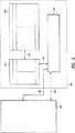
図1は、本発明に関する半導体記憶媒体を実装するためのアーキテクチャーを示している。記憶媒体は、ホストまたは、他の外部デジタルシステムとの利用のためのものである。大容量記憶装置は、揮発性RAMアレイ100及び不揮発性アレイ104の二つの部分に区分される。好ましい実施態様によると、不揮発性メモリ記憶装置の全てはフラッシュである。フラッシュはEEPROMによって置き換えられ得る。RAMは任意の都合の良いタイプである。
メモリ記憶装置104は、データを0からN-1までのNブロックに編成する。データの各ブロックは、Mバイト長である。好ましい実施態様では、各データブロックは512バイト長で、市販利用されているハードディスクドライブにおけるセクタ長に対応しており、さらにフラグ、論理ブロックアドレス情報(LBA)及び関連したECCを格納するための余剰バイトを有する。メモリ104はユーザが必要とするメモリ記憶装置と同じ容量を有し得る。大容量記憶装置の例には、100Mバイトのアドレシングが可能な記憶装置も含み得る。
RAMロケーション102は複数ある。各RAMロケーション102は、ホストシステムまたは、不揮発性媒体の実際の物理アドレスによって与えられる論理ブロックアドレスの適切な一つを用いてコントローラによって一意にアドレスされる。RAMロケーション102は論理ブロックアドレスに関連するデータ及び、不揮発性媒体の物理ブロックアドレスに関連するフラグの物理ブロックアドレスを有する。
物理ブロックアドレス(PBA)は図2に示されるように、二つのフィールドに分割され得る。これらのフィールドはデータブロックのグループのクラスタアドレスのために使用され得る。第1のフィールド290は、クラスタアドレスを選択するために用いられ、第2のフィールド292は、このクラスタに関連する論理ブロックアドレスのスタートアドレスを選択するために用いられ得る。
情報フラグの集まりもまた、各不揮発性メモリロケーション106のために格納されている。これらのフラグは、旧/新フラグ110、使用中/フリーフラグ112、欠陥フラグ114、及びシングル/セクタフラグ116を含む。さらに、データ格納(領域)112も有する。
本発明の大容量記憶装置にデータを書き込む時、コントローラはデータを格納するための第1の利用可能な物理ブロックを決定する。ホストによって選択された論理ブロックアドレスに対応するRAMロケーション102は、104(図1)内の不揮発性メモリアレイ内部のデータが実際に格納される物理ブロックアドレス内に書き込まれる。
ユーザがワープロ文書を準備し、コンピュータに文書の保存を指示する例を考える。文書は大容量記憶システム内に格納される。ホストシステムは大容量記憶システムに論理ブロックアドレスを割り当てる。本発明の大容量記憶システムは未使用ブロックまたは、文書を格納するための大容量記憶装置内ブロックの物理アドレスを選択する。物理ブロックアドレスのアドレスは、論理ブロックアドレスに対応してRAMロケーション102に格納される。データがプログラムされると、本発明のシステムはまた、104及び293において使用中フリーフラグ112をこのブロックロケーションは使用中であることを示すように設定する。1つの使用中/フリーフラグ112は不揮発性アレイ104の各エントリのために提供される。
さらに、ユーザが文書を取り出し、変更を加え、再度コンピュータに文書を格納する指示を与えると仮定する。書き込み前消去サイクルを回避するため、本発明のシステムは、関連するブロックが消去されることを示す未設定の(プログラムされていない)100内の使用中/フリーフラグ112を有するブロックをロケーションづけるための手段を提供する。システムはその時、106の新ブロック112、100の新ブロック293のための使用中/フリーフラグ112を設定し、その後、不揮発性アレイ104内の新しい物理ブロックロケーション106内に修正された文書を格納する。新しい物理ブロックロケーションのアドレスもまた、論理ブロックアドレスに対応するRAMロケーション102に格納され、102内で以前の物理ブロックロケーションに上書きされる。次にシステムは以前のバージョンの文書の旧/新フラグ110を設定し、これにより104の110及び109の293で不必要な古いバージョンの文書を示す。この様に、本発明のシステムは、以前の文書の修正バージョンを格納するために従来システムの書き込み前消去において必要とされる消去サイクルのオーバーヘッドを回避する。
RAMアレイ100は電源停止状態でその記憶を失うため、媒体の実際の物理ブロックアドレスを持つ論理ブロックアドレスはまた、不揮発性アレイ104においてシャドウメモリ108として格納される。コントローラによってシャドウ情報が適切なRAMロケーション102に格納されることがわかる。電源が供給される間、100のRAMロケーションは、104の情報106を読み込むことで104における全ての物理ロケーションから適切に更新される。106の論理アドレス108は100のRAMロケーションをアドレスするために用いられ、所与の論理ブロックアドレスに関連する実際の物理ブロックアドレスを更新する。また106は新しいデータ122に関連する実際の物理ブロックアドレスであるため、フラグ110、112、114及び、116は100の物理ブロックアドレス106を用いて102の293内で更新される。フラグが適当な不揮発性メモリロケーション106または、不揮発性メモリロケーションと物理ブロックアドレスに関連するRAMロケーション102の両方のいずれかで格納され得ることが当業者には明らかである。
パワーアップ時に、揮発性メモリ100内の論理ブロックアドレスに割り当てられる最新の物理ブロックアドレスを割り当てるために、コントローラはまず、不揮発性メモリ104のフラグ110、112、114及び116部分を読み込み、揮発性メモリ100内のフラグ部293を更新する。次にコントローラは、不揮発性媒体104の全ての物理ブロックアドレスの論理ブロックアドレス108を読み込み、揮発性メモリ100内の所与の物理ブロックアドレスのフラグを把握することで、不揮発性メモリ104内の物理ブロックアドレスの読み込み論理ブロックアドレスを読み込み、揮発性メモリ100内の読み込み論理ブロックアドレスを読み込むために割り当てられた最新の物理ブロックアドレスを更新し得る。
図3は、本発明の大容量記憶装置を組み込んだシステムのブロック図を示す。ホストコンピューター、パソコンのような外部デジタルシステム300は、本発明の大容量記憶装置302に接続されている。論理ブロックアドレスはアドレスバス306を介して揮発性RAMアレイ100及び、コントローラ回路304に接続されている。制御信号はまた、コントロールバス308を介してコントローラ304に接続されている。揮発性RAMアレイ100は、不揮発性RAMアレイ400に物理ブロックアドレスを提供するために接続されている。コントローラ304は、揮発性RAM100と不揮発性アレイ104の両方を制御するために接続され、全てのフラグを生成する。
本発明に関する書き込み処理の動作を示す、単純化された例は、図4から図8に示される。過剰な説明によって発明の特徴をわかりにくくしない様に全ての情報フラグを表記していない。データエントリは、本発明の理解を更に単純化するために10進数で示している。好ましい実施態様では、2進法が使用されていることが当業者には明らかである。
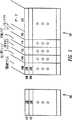
図4は、本発明に関する11のエントリを持つ大容量記憶装置を示す。図4の大容量記憶装置内に有効なまたは、使用可能なデータは格納されていない。従って、全ての物理ブロックアドレスは空である。不揮発性大容量記憶装置のロケーション’6’に格納されたデータは詰まっており、古いものである。さらに、ロケーション’9’には欠陥があり、使用できない。
ホストは大容量記憶装置に例として、論理ブロックアドレス’3’、次に’4’に順次データの書き込みを指示する。大容量記憶装置はまず、論理ブロックアドレス’3’に関連するデータを書き込む。装置は不揮発性メモリ内で最初の未使用ロケーションを決定する。この例では、最初の空いている場所はロケーション’0’である。
従って、図5は論理ブロックアドレス’3’に対して対応する物理ブロックアドレス’0’が格納され、使用中フラグが物理ブロックアドレス’0’に設定される事を示している。次の空いている場所はロケーション’1’である。図6は、論理ブロックアドレス’4’に対して対応する物理ブロックアドレス’1’が格納され、使用中フラグが物理ブロックアドレス’1’に設定される事を示している。
ホストは論理ブロックアドレス’3’に何かを再び書き込むことを指示する。次の空いている場所は、ロケーション’2’であると決定される。図7では、データがもはや使用不可能であり、使用中フラグがロケーション’2’に設定され、ロケーション’3’における物理ブロックアドレスが’2’に変更されたことを示すように、ロケーション’0’における旧フラグが設定される事を示している。
さらに、ホストは論理ブロックアドレス’4’に再度何かを書き込むことを指示する。次の空いている場所はロケーション’3’であると判断される。図8では、データがもはや使用不可能であり、使用中フラグがロケーション’3’に設定され、ロケーション’4’における物理ブロックアドレスが’3’に変更されたことを示すために、ロケーション’1’の旧フラグが設定される事を示している。(物理ブロックアドレスと同じロケーションに格納されたデータとの間には一般に何ら関係がないことを思い出されたい)。
図9は、本発明に関するアルゴリズム1を示している。本発明のシステムがデータを大容量記憶装置にプログラムするよう指示を受けた時(ステップ200)、その時システムはフリーブロック、即ち設定されていない(プログラムされていない)使用中/フリーフラグを持つブロックを見つけ出そうとする。見つかった場合、システムはそのブロックのための使用中/フリーフラグを設定し、データをそのブロック内にプログラムする(ステップ206)。
一方、システムが設定されていない使用中/フリーフラグを持つブロックを見つけ出せない場合、システムはフラグ(使用中/フリー及び、旧/新)及び、設定されている旧/新フラグ有する全ブロックに対するデータ及び、設定されていない欠陥フラグを消去し(ステップ204)、次に未設定の使用中/フリーフラグを有するブロックを検索する(ステップ202)。そのようなブロックはステップ204によって生成されるだけである。システムは次に、そのブロックのための使用中/フリーフラグを設定し、データファイルをそのブロックにプログラムする(ステップ206)。
もしデータが、これまでに存在するファイルの修正されたバージョンである場合、システムはアクセスされているものから入れ替えられたバージョンを防がなければならない。システムは、データファイルが旧データファイルを入れ替えるかどうか判断する(ステップ208)。もし入れ替えるならば、システムは入れ替えられたブロックに関連する旧/新フラグを設定する(ステップ210)。一方、格納されたデータファイルが新規作成されたデータファイルの場合、旧/新フラグの設定ステップ(ステップ210)は、入れ替えられるブロックがないためスキップされる。最後に、論理アドレス308−を物理アドレスに相互関係づけるマップが更新される(ステップ212)
こでまでに概説した手順に従って、周期的な場合を除いてメモリ104への各書き込みに対して消去サイクルに伴うオーバーヘットが回避される。これによって、本発明のアーキテクチャーを使用したコンピュータシステム全体のパフォーマンスが画期的に改善される。
本発明の好ましい実施態様では、フラッシュメモリのプログラミングは、当業者よって一般に知られている手順に従っている。言い換えると、プログラムのインパルス(Impulse)により、ビットに適切にプログラムされるよう適用され、適切なプログラミングが行われたことを確認するためにプログラムされたデータを比較する。最終的にビットは消去または、正しくプログラムされず、欠陥フラグ148はそのブロックが再度使用されないように設定される。
図10は、本発明の代替の実施形態を用いるデジタルカメラ等のデジタルシステム500を示す。ホスト502を含むようにデジタルシステム500を示すが、ホスト502はパーソナルコンピュータ(PC)、または単に、デジタルシステムにおいて通常用いられる任意の一般的なタイプのプロセッサであり得、不揮発性メモリユニット508に情報を格納するか、または不揮発性メモリユニット508から情報を取り出すための制御回路506に結合される。制御回路506は半導体(あるいは「集積回路」または「チップ」と呼ぶ)、またはさまざまな電子部品を自由選択的に組合せたものであり得る。好適な実施形態において、制御回路を単一のチップデバイスとして示す。不揮発性メモリユニット508は1つ以上のメモリデバイスから構成され、メモリデバイスはそれぞれフラッシュ型またはEEPROM型のメモリであり得る。図10の好適な実施形態において、メモリユニット508は、複数のフラッシュメモリデバイス510〜512を含み、各フラッシュデバイスは、情報を格納するための別個にアドレス可能なロケーションを含む。図10の実施形態の好適なアプリケーションにおいて、このような情報は、それぞれが1つ以上のデータのセクタを有するブロックに組織される。データに加えて、格納された情報は、フラグフィールドおよびアドレス情報等の、データブロックに関するステータス情報をさらに含み得る。
ホスト502は、ホスト情報信号504を介して制御回路506に結合される。ホスト情報信号は、アドレスおよびデータバス、ならびに、コマンド、データおよび他のタイプの情報を制御回路506に通信するための制御信号からなり、制御回路506はフラッシュアドレスバス512、フラッシュデータバス514,フラッシュ信号516およびフラッシュステータス信号518(508および512〜516を集合的に信号538と呼ぶ)を介してこのような情報をメモリユニット508に順に格納する。信号538は、コントローラ506およびメモリユニット508との間にコマンド、データおよびステータス情報を提供し得る。
図示するコントローラ506は、ホストインターフェースブロック520、バッファRAMブロック522、フラッシュコントローラブロック532、マイクロプロセッサブロック524、マイクロプロセッサコントローラブロック528、マイクロプロセッサ格納ブロック530、マイクロプロセッサROMブロック534、ECC論理ブロック540、およびスペースマネジャーブロック544等の高レベル機能ブロックを含む。ホストインターフェースブロック520は、バッファRAMブロック522およびマイクロプロセッサブロック524からのデータおよびステータス情報をホスト情報信号504を介してホスト502に提供するためのホスト情報信号504を受け取る。ホストインターフェースブロック520は、マイクロプロセッサ情報信号526を介してマイクロプロセッサブロック524に結合される。マイクロプロセッサ情報信号526は、アドレスバス、データバスおよび制御信号から構成される。
図示されるマイクロプロセッサブロック524は、マイクロプロセッサコントローラブロック528、マイクロプロセッサ格納ブロック530、マイクロプロセッサROMブロック534に結合され、そして、マイクロプロセッサ格納ブロック530およびマイクロプロセッサROMブロック534に格納されたプログラム命令を実行することによって、コントローラ506内の図10に示すさまざまな機能ブロックの動作を指示する役割を果たす。マイクロプロセッサブロック524は、適切な時点にマイクロプロセッサROMブロック534からのプログラム命令(またはコード)を実行し得る。なお、マイクロプロセッサROMブロック534は不揮発性格納領域である。一方で、マイクロプロセッサ格納ブロック530は、揮発性、つまり読み出しおよび書き込みメモリ(RAM)、もしくは不揮発性、つまりEEPROM型のメモリ記憶装置のいずれかであり得る。マイクロプロセッサブロック524によって実行された命令を集合的にプログラムコードと呼ぶが、これらは本発明のシステムの動作の開始に先立つある時点で格納ブロック530に格納される。始めに、かつ、マイクロプロセッサ格納ロケーション530からのプログラムコードの実行に先立って、プログラムコードはメモリユニット508内に格納され、その後、信号538を介して格納ブロック530にダウンロードされ得る。この初期化の間に、マイクロプロセッサブロック524はROMブロック534からの命令を実行し得る。
コントローラ506は、マイクロプロセッサの指示の下、メモリユニットに情報を提供するまたはメモリユニットから情報を受け取るためにマイクロプロセッサ情報信号526を介してマイクロプロセッサブロック524に結合されたフラッシュコントローラブロック532をさらに含む。データ等の情報は、フラッシュコントローラブロック532からマイクロプロセッサ信号526を介してバッファRAMブロック522に提供されて、そこに格納され得る。(単に一時的な格納であってもよい。)同様に、マイクロプロセッサ信号526を介して、データはフラッシュコントローラブロック532によってバッファRAMブロック522から取り出され得る。
ECC論理ブロック540は、信号542を介してバッファRAMブロック522に結合され、そして、マイクロプロセッサ信号526を介してマイクロプロセッサブロック524にさらに結合される。ECC論理ブロック540は、通常エラーコーディング機能およびエラー訂正機能を実行するための回路機構を含む。さまざまなECC装置およびアルゴリズムが市販されており、ECC論理ブロック540に要求される機能を実行するために用いられ得ることが当業者によって理解されるべきである。要するに、これらの機能は、あらゆる集中的な目的のために多項式から独自に生成されたコードを伝送中のデータに添付することを含み、データが受け取られた場合には、同じ多項式を用いて、データを破壊し得る所定の数のエラーを検出し、かつ、潜在的に訂正するための受け取られたデータから別のコードを生成する。ECC論理ブロック540は、メモリユニット508に格納されたデータまたはホスト502から受け取られたデータについて、エラー検出動作および/またはエラー訂正動作を行う。
スペースマネジャーブロック544は、1ブロックの情報を格納するための1つのフラッシュメモリデバイス内に、次の使用されていない(またはフリーの)格納ブロックを見つけるために、好適な装置およびアルゴリズムを用いる。これについては、他の図面を参照して本明細書中でさらに説明する。既に説明したように、1つのフラッシュメモリデバイス内の1ブロックのアドレスをPBAと呼ぶが、PBAは、ホストから受け取られたLBAについての翻訳を実行することによって、スペースマネジャーによって決定される。この翻訳を達成するために、さまざまな装置および方法が使用され得る。このようなスキームの一例が、”Flash Memory Mass Storage Architecture Incorporating Wear Leveling Technique Without Using CAM Cells”という名称の米国特許第5,485,595号に開示されており、この文献の明細書を本明細書中で参考として援用する。他のLBAからPBAへの翻訳方法および装置を、本発明の範囲および精神から逸れることなく同様に用い得る。
スペースマネジャーブロック544はSPM RAMブロック548およびSPM制御ブロック546を含み、SPM RAMブロック548およびSPM制御ブロック546は結合されている。SPM RAMブロック548は、SPM制御ブロック546の制御下で、LBA-PBAマッピング情報(あるいは、本明細書中では翻訳テーブル、マッピングテーブル、マッピング情報、またはテーブルと呼ぶ)を格納する。あるいは、SPM RAMブロック548は、RAMアレイ100について図3に示すように、コントローラの外部に位置し得る。
動作において、ホスト502は、例えばコントローラ506を介した読み出し動作または書き込み動作の実行の間に、メモリユニット508に情報を書き込み、かつ、メモリユニット508から情報を読み出す。それを行う際に、ホスト502は、ホスト信号504を介してコントローラ506にLBAを提供する。LBAはホストインターフェースブロック520によって受け取られる。マイクロプロセッサブロック524の指示の下、LBAは最終的にはスペースマネジャーブロック544に提供されて、PBAに翻訳され、そしてそこに格納される。これについては、後でさらに詳細に説明する。
マイクロプロセッサブロック524の指示下で、データおよび他の情報は、フラッシュコントローラブロック532を介してフラッシュメモリデバイス510〜512のうちの1つにある、PBAによって識別される格納領域に書き込まれるか、または格納領域から読み出される。既に説明したように、フラッシュメモリデバイス内に格納された情報は、まず消去しなければ新たな情報によって上書きされ得ない。一方で、(常に書き込みに先行する)1ブロックの情報の消去は、時間と電力を大幅に消費する手段である。これは時々、書き込み前消去動作と呼ばれる。好適な実施形態は、フラッシュメモリ内のPBAロケーションからメモリユニット508内の未使用のPBAロケーションに再び書き込まれている、ブロック内の、情報のセクタ(または多重セクタ)を連続して、しかし、効率的に移動することによりこのような動作を除去し、そうすることにより、頻繁な消去動作を除去する。1ブロックの情報は、16個または32個のセクタ等の、1を超える数のセクタから構成され得る。1ブロックの情報は、情報の別個に消去可能なユニットになるようにさらに規定される。過去、従来技術のシステムは、フラッシュメモリデバイス内のフリーの(または未使用の)ロケーション内に既に書き込まれている、フラッシュメモリデバイス内に格納されたブロックを移動させる。しかし、このようなシステムは、そのブロック内の1セクタの情報が再び書き込まれる場合でさえ、ブロック全体を移動させた。換言すると、ブロック内のセクタの合計数よりも少ない数のセクタが再び書き込まれている場合には、ブロック全体の内容を移動するのに時間が無駄であるのに加えて、フラッシュメモリ内の記憶容量も無駄になる。本発明の好適な実施形態は、本明細書中で説明するように、1ブロックの情報よりも少ない数の「移動」を可能にすることにより、既に書き込まれたセクタの移動動作の数を減らして、結果的に消去動作の数を減らす。
図10を参照すると、SPM RAMブロック548が、書き込み動作が行われる毎に変更され得るテーブルを維持することによって、LBA-PBAマッピング情報およびメモリユニット508に格納されている各ブロックに関する他の情報を維持することに留意することは重要である。加えて、このマッピング情報は、フラッシュメモリデバイス内における情報の(ブロック内の)セクタの実際のロケーションを提供する。さらに明らかなように、システムへの電力が妨害または終了される場合に、マッピング情報の損失を防ぐために、SPM RAMブロック548に格納されたマッピングテーブル内の情報の少なくとも一部分が、メモリユニット508に「シャドウイング(shadowed)される」(またはコピーされる)。これは、大部分に、マッピング情報を維持するために揮発性メモリを使用することに起因する。これに関して、システムへの電力が回復された場合、マッピング情報の、メモリユニット508に格納された部分はSPM RAMブロック548に転送される。
SPM RAMブロック548は、あるいは、フラッシュまたはEEPROMメモリアーキテクチャの形態等の不揮発性メモリであってもよいことに留意されたい。この場合、不揮発性メモリに格納されたマッピング情報は停電の間も正確に維持されるので、マッピングテーブルは不揮発性メモリ内に格納されることにより、「シャドウイング(shadowing)」の必要が除去される。
1つ以上のセクタがフラッシュメモリのある領域から別の領域へと移動されている場合、本発明の好適な実施形態は、まずセクタを、それらがフラッシュメモリデバイス、つまり、510〜512内に格納されているロケーションから、バッファRAMブロック522へと移動させ、そこに一時的に格納する。移動されたセクタは次にバッファRAMブロック522から1つのフラッシュメモリデバイス内のフリーの領域に移動される。ECC論理ブロック540によって生成されたECCコードは、上で説明したように、他の情報のように、データおよびフラグフィールドに対応するLBA等のデータと共にフラッシュメモデバイス510〜512内にも格納される。
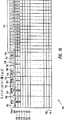
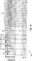
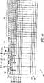
図11〜図21は、メモリユニット508内のブロック(およびブロック内のセクタ)の識別およびロケーションに関するLBA-PBAマッピング情報を格納するように構成されたSPM RAMブロック548内のテーブル700の状態の例を示す。これらの図面の全てにおいて、テーブル700は示され、列および行からなるアレイを含み、列は、仮想物理アドレスロケーションまたはVPBAブロックアドレスロケーション702、移動仮想物理ブロックアドレスロケーションまたはMVPBAブロックアドレスロケーション704、移動フラグロケーション706、使用中/フリーフラグロケーション708、旧/新フラグロケーション710、欠陥フラグロケーション712、およびセクタ移動ステータスロケーション714を含む。
テーブルの行は、PBA/LBA行716および718〜728を含み、各行は、テーブル700内のアドレスされている情報に基づくLBAまたはPBAのいずれかであり得る行番号を有する。例えば、行716は行番号「00」が割り当てられているように示され、LBA「00」に関するPBA情報がテーブル700から取り出されている場合、次にLBA「00」は行716におけるSPM RAMブロック548においてアドレスされ得、730内に位置する関連するPBAを得ることができる。一方で、フラグフィールド706〜712等の、あるブロックに関するステータス情報がアクセスされている場合、「00」、「10」、「20」、「30」、「40」、「50」、「N-1」等の、行716〜728の行番号は、LBAと反対の、PBAの値を示す。さらに、テーブル700の各行は、各エントリがブロックに関する情報を含む、ブロックエントリとして考慮され得る。さらに、テーブル700の各行は、LBAによってアドレスされ得る。
好適な実施形態において、各ブロックは16個のセクタを含むように示される。これは、16個のセクタからなるブロック全体を選択的に消去する能力に起因するものである。(これが理由で、ブロックのサイズを「消去ブロックサイズ」と呼ぶことがある。)図11〜図21に示すように、消去ブロックサイズが16セクタである場合、各ブロックエントリ(または行)は16個のセクタに関する情報を含む。従って行716は、LBA「00」〜LBA「15」(または16進法でLBA「00」〜LBA「0F」)によってアドレスされたブロックに関する情報を含む。次の行、つまり行718は、LBA「16」(または16進法で「10」)〜LBA「31」(または16進法で「1F」)によってアドレスされたブロックに関する情報を含む。同じことが各ブロックのPBAについても当てはまる。
しかし、他のブロックサイズを同様に用いてもよいことに留意されたい。例えば、ブロックは32個のセクタを含み、従って消去ブロックサイズ32を含み得る。後者の状況において、716、718、720...等の各ブロックエントリまたは行は、32個のセクタに関する情報を含み、ここで、各ブロックは16個のセクタからなる。(16セクタブロックサイズ以外のサイズが同様に使用され得る。)
テーブル700のVPBAブロックアドレスロケーション702は、通常、特定のLBA値に対応するPBA値を示す情報を格納する。MVPBAブロックアドレスロケーション704は、メモリユニット508内で、ブロック(またはそのセクタ部分)が移動され得た場所のロケーションを識別するPBA値を示す情報を格納する。移動フラグロケーション706は、アクセスされているブロックが、MVPBAブロックアドレスロケーション704内の値によってPBAが標識されたロケーションに移動し得た任意のセクタを有するかどうかを示す値を格納する。(704内のPBA値は、残りのブロックアドレス情報が位置し得るVPBAブロックアドレス702に示された値とは異なる。)使用中/新しいフラグロケーション708が情報を格納して、アクセスされているブロックがフリーのブロックであるかどうか、つまりブロックが最後に消去されたのでデータが格納されていないことを示す。旧/新フラグロケーション710は、ブロックが使用され、そして再び使用され、従って古いかどうかについて、アクセスされているブロックのステータスを示す情報を格納する。欠陥フラグロケーション712は、ブロックが欠陥であるかどうかに関する情報を格納する。ブロックが欠陥であると表される場合、設定されている欠陥フラグロケーション712の値によって示されるように、欠陥ブロックはこれ以上使用することができない。フラグ708〜712は、図1について図示され、かつ、説明されたフラグ110〜114と同様である。
セクタ移動ステータスロケーション714は16ビットからなり(ロケーション714はブロック内の各セクタに対して1ビットを含むので、異なるサイズのブロックについては、ロケーション714内に異なる数のビットが要求される)、各ビットは、セクタがメモリユニット508内の別のブロックに移動したかどうかについてブロック内のセクタのステータスを示す。メモリユニット508内の移動されたブロックロケーションは、VPBAブロックアドレスロケーション702内のPBA値ではなくPBAによって識別される。異なって述べたように、ブロック内のセクタが移動したかどうかのステータスは、714内のビットの各々によって示されるように、VPBAブロックアドレスロケーション702またはMBPBAブロックアドレスロケーション704のいずれ一方が、セクタに関する最も最近のPBAロケーションを維持するのかを示す。
さらに図11を参照すると、例を用いて、LBA「0」が書き込まれている場合の、SPM RAMブロック548(図10)に格納されたテーブル700のステータスの例が示される。既に述べたように、本明細書中で提示する図面において、16個のセクタ(10進法で0〜15、または16進法で0〜10)からなるブロックサイズは、例を説明するためのみに使用される。同様に、N個のブロック(従ってN個のLBA)が使用され、0〜N-1までの番号が与えられる。ブロックサイズおよびブロックの数は、異なるアプリケーションについて変化し得、かつ、使用されている別個のフラッシュメモリデバイス(510〜512等)の各々のメモリ容量に依存し得る設計上の選択事項である。さらに、これらの実施例において512バイトの好適なセクタサイズが使用されるが、本発明の範囲および精神から逸れることなく他のセクタサイズを使用し得る。
フラッシュメモリデバイス510〜512(図10)内の全てのブロックが消去され、従ってフリーになった場合には、初期化、または、システムパワーアップの前にLBA「0」への書き込み動作が行われると仮定する。スペースマネジャーブロック548は、次のフリーのPBAロケーションが「00」であると判定しようとする。従って「00」は、LBA行番号「00」によってテーブル700に示されるように、LBA「0」に関する情報が維持されている、行716のVPBAブロックアドレス702内の730へ書き込まれる。LBA0ブロック内のセクタのいずれも移動する必要がないので、ロケーション732として示す、行716についてのMVPBAブロックアドレス704は、初期値などの任意の値を含み得る。(図11において、「XX」は「注意する必要のない」状態(”don’t care”state)を示すものとして図示される。)
734の値は論理状態「0」にあり、LBA「0」ブロックがいかなる移動されたセクタも含まないことを示す。行716の使用されたフラグ708列内のロケーション736は、PBA「0」ブロックが使用中であることを示す論理状態「1」に設定される。ロケーション738の状態は、行716について古いフラグ710を示しているが、「0」に設定されて、PBA「0」ブロックがまだ「古く」はないことを示す。ロケーション740は、PBA「0」ブロックが欠陥ではないことを示す論理状態「0」を維持し、そして、移動ステータスロケーション714における全てのビットが論理状態「0」にあって、LBA「0」ブロック〜LBA「15」ブロック内のセクタのどれも移動していないことを示す。
図11において、テーブル700の、全ての残りの行716〜728について、移動フラグロケーション706、使用されているフラグロケーション708、古いフラグロケーション710、欠陥フラグロケーション712、および移動ステータスロケーション714等の、行716内のLBA「0」についてのステータス情報は、論理状態「0」にある。システムのパワーアップ時および/または任意のブロックの消去後に、消去されたブロックについてのエントリは、テーブル700において、パワーアップ時の全てのブロックであるが、これらは全て論理状態「0」に設定される。
このとき、LBA「0」ブロックが配置され得るメモリユニット508内のフラッシュメモリデバイスのうちの1つについての内容の説明は、図11のテーブル700に示すマッピング情報のより良い理解のために提示される。
ここで図22を参照すると、(図11に示すように)テーブル700の状態に従ってフラッシュメモリデバイス510の内容の例を示す。LBA「0」は、メモリユニット508内で(図10の)コントローラ506によってPBA「0」において識別されるが、これはホスト識別ブロック(host-identified block)が書き込まれたロケーションである。セクタデータロケーション752内のデータを含むPBA0行750を図22に示す。PBA0行750のECCロケーション754にECCコードがさらに格納される。このECCコードは、既に説明したように、書き込まれているデータに関連するECC論理ブロック540によって生成される。PBA0行750のフラグフィールド756は、書き込まれているブロックのセクタデータに対応する、移動の、使用中、古い、そして欠陥のフラグ情報を含む。本実施例において、フラグフィールド756内に、「使用された」フラグのみが設定され、他のフラグが設定されない、従ってフラグフィールド756は、PBA「0」は「使用された」が、「移動」しておらず、「古く」なく、または「欠陥」のないことを示す「0100」の論理状態を維持する。
PBA0行750は、LBAアドレスロケーション758を維持するための格納ロケーションをさらに含み、PBA「0」に対応するLBA番号は、本実施例では「0」である。当面、この例に関連しない間は、LAB「0」の残りのPBAロケーションは、フラッシュメモリデバイス510内の行750に続く次の15行に格納される。
本明細書中に提供された本実施例の説明から、フラッシュメモリデバイス510のPBA行内の情報が、特に、フラッシュメモリの各PBA行(750、762、764...)内に「移動」フラグが存在することに起因して、データおよびステータス情報に関連する任意の移動を含むLBA「0」ブロック内のデータおよびステータス情報に関するデータおよびステータス情報を識別するのに十分であることが理解される。にもかかわらず、それとは異なり、別のフィールドが、フラッシュ内の各LBAロケーションの第1のPBA行に追加され得、テーブル700内の対応する行の移動ステータスロケーション714内のビットのステータスを複製する。このフィールドは、図22に示すセクタステータスロケーション760内に、行750および780等の各LBAブロックの第1のPBA行内に含まれるように自由選択的に格納される。ロケーション760内に維持される情報は、各PBA行のフラグフィールド756内の「移動」フラグのステータスをチェックすることにより発見され得るが、ロケーション760を用いることの明白な利点は、読み出し動作がより少ないために、システムの始動(または電源オン)時に、SPM RAMブロック548内のテーブル700の内容は、より速く更新され得る。(テーブル700はSPM RAMブロック548内に維持され、SPM RAMブロック548は、システムがパワーダウンし、そして不揮発性メモリ、つまりメモリユニット508からのパワーアップ時に更新される必要のある場合にその内容が失われれる揮発性メモリであることを思い出されたい。)
つまり、全てのPBA行(好適な実施例では合計16行)を読み出して、パワーアップ時にテーブル700の各LBAエントリを更新するよりも、各LBAの第1のPBA行のみがフラッシュメモリから読み出され、そして、SPM RAM548に格納されることが必要であり、それにより、不必要な読み出し動作を除去することにより時間を節約する。一方で、LBAにつき16ビットのセクタステータス情報を維持するために、明らかにより多くのメモリ容量が利用される。
ロケーション760が使用される上記実施例において、セクタステータスロケーション760の値は全て「0」(または16進法で「0000」)である。
フラッシュメモリデバイス510において、行750、762、764、768...の各々は、PBAロケーションであり、各行は、PBA行番号を有し、そして、特定のLBAによってアドレスされたブロック内のセクタについてのデータおよび他の情報(データおよび他の情報は行750について上で説明した通りである)を格納するものである。さらに、16個の順次的PBA行のそれぞれが1ブロックの情報を示す。つまり、PBA行750、762、および764〜768は、16行のPBA行を示すことが意図されるが、(図11のテーブル700内の行716として示される)LBA0に対応し、そして、PBA行の各々がブロック内のセクタに関する情報を維持する。情報の次のブロックは、マッピング情報がテーブル700の行718に含まれ、そして、フラッシュメモリデバイス510等において、(16進法で)「10」(または10進法で「16」)から開始して(16進法で)「1F」(または「31」)で終了するロケーション内に格納された、LBA「10」(16進法)によってアドレスされたブロックに関する。
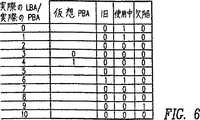
上記例を続けて説明すると、図12は、LBA0がホストによって再び書き込まれている場合のテーブル700の状態の一例を示す。LBA0は既に書き込まれており、かつ、始めに消去されずに再び書き込まれるので、メモリユニット508内の別のフリーのロケーションは(ここで、それぞれセクタを含むブロックが、例えば、デバイス510に続く次のフラッシュメモリデバイスが、フラッシュメモリデバイス510が省かれたPBAアドレスされたブロックをピックアップし、このことの一例として、フラッシュメモリデバイス510が0〜FF(16進法)のPBAを含み、そして、512であり得る次のフラッシュメモリデバイスが100〜1FF(16進法)を含み得るように、それぞれのPBAに基づいて、メモリユニット508のフラッシュメモリデバイスの各々を介して、順次、かつ連続的に組織されることに留意することが役に立ち得る)、新たな情報を格納するためにスペースマネジャー544によって配置される。このフリーのロケーションは、(16進法で)PBA「10」(または10進法で16)となるように示される。PBA「10」が現在は「使用中」であることを示すように、ロケーション742内の使用されたフラグが設定されている(本発明から逸れることなく反対の極性が使用され得るが、好適な実施形態において、論理状態「1」である場合にフラグが設定される)ことを除いて、行718において、LBA「10」についてのエントリは、図11に示されるように、同じままである。
行716内のエントリは、MVPBAブロックアドレスロケーション732内に「10」を示すように変更され、MVPBAブロックアドレスロケーション732は、LBA「00」ブロックについての移動した部分のPBAアドレスを提供する。ロケーション734内の移動フラグは論理状態「1」に設定されて、少なくとも一部分(1つ以上のセクタ)のLBA「00」ブロックが、テーブル700のロケーション730内に示されるPBAロケーションとは異なるPBAロケーションに移動したことを示す。最終的に、行716内の移動ステータスロケーション714のビットは、(2進法で)「1000000000000000」(16進法で「8000」)に設定され、ブロックLBA「00」内の移動したセクタのステータスを反映する。つまり、この例において、「8000」は、LBA「00」ブロック内の第1のセクタまたはセクタ「0」が、異なるPBAロケーションに移動したことを示す。
ここで図22を参照すると、図12におけるテーブル700の状態は、LBA「0」ブロックの移動されたセクタがここで行780のPBA「10」に書き込まれるという点で、フラッシュメモリデバイス510の内容に影響する。行780は移動されたセクタに関するデータを含む。移動されたセクタは512バイトのサイズを有する。移動されたセクタ情報について、行780はECCコード、(図12の)テーブル700のフラグロケーション734〜740内の値のコピー、および行780内のデータがLBA「00」に属することを示すLBA「00」とをさらに含み、そして、LBA「0」ブロック内の個々のセクタの各々についての移動ステータスをさらに含み得る。
図面には特定的には示さないが、PBA行750のロケーション756内の移動フラグは、対応するブロックの少なくとも一部分が移動されたことを示すように設定される。行716の移動ステータスロケーション714内に格納された値は(図12)、16進法で「8000」であるが、これは行750のロケーション760内にも格納される。既に述べたように、このことは、PBA「0」のセクタ「0」のみが「移動された」とマークされ、そして、新たなブロックLBA「0」がフラッシュメモリ内のPBA「10」に書き込まれたことを示す。図22のさらに詳細な説明がなくても、同様に以下の例がフラッシュメモリデバイス510の内容に影響することを理解されたい。
図13は、LBA「00」へのさらに別の書き込み動作が実行される場合のテーブル700のステータスを示す。行716内の値(またはエントリ)は、ロケーション732内の値が(16進法で)「20」に変化して、ブロックLBA「00」の移動された部分がこのとき(図12の「10」ではなくて)PBAロケーション「20」に配置されることを示す以外は、図12と同じままである。図12のように、移動ステータスロケーション714内の値「8000」は、(PBA「00」を有する)第1のセクタがブロックの移動された部分であることを示す。
行718は、LBA「10」ブロックがこの時点では古く、そして、消去されるまではこれ以上使用できないことを示すように変更される。これは、論理状態「1」に設定されているロケーション744内の値によって示される。LBA「20」についてのエントリ、つまり行720は、ロケーション746が、使用中であるPBA「20」ブロックの状態を反映する論理状態「1」に設定されるように変更される点を除いては、変わらないままである。図11および図12のように、上で説明せず、かつ、図13における特定の論理状態を有するものとして示さなかった、図13のテーブル700の残り全ての値は、全て変わらないままである(フラグは全て論理状態「0」に設定される)ことを理解されたい。
さらに上の例について続けると、図14は、LBA「0」に対するさらに別の書き込みが行われる場合のテーブル700の状態を示す。比較を容易にするために、図14に示す値で、図13に示した状態に対して異なる論理状態にあるものをを円で囲んだ。行716において、ロケーション732内に示す、PBA「30」として示された、新たに移動されたロケーションを除いては、全て同じままである。PBA「30」は、スペースマネジャー544によって見つけられた次の空いたロケーションであった。既に述べたように、この値は、LBA「0」のブロックの部分がこの時にはPBA「30」にある、つまり、そのブロック内の、(「8000」である行716の714内の値によって示される)第1のセクタがフラッシュメモリデバイス510内のPBA「30」に移動したことを示す。
行718は消去されるまでは同じままである。ロケーション742および744内のフラグは、論理状態「0」に設定される。行720も、その古いフラグ710列内の値が、PBA「20」のブロックも古く、まず消去しなければ使用できないことを示すように、「1」に変更されていることを除いては、変わらないままである。行722は、その使用されたフラグ708列内の値は、論理状態「1」に変化して、LBA「30」のブロックが現在使用中であることを示すこと以外は、同じままである。
図15は、テーブル700の状態の別の例であり、テーブル700は、テーブルが図13に示す状態にあり、ホストのLBA「5」への書き込みがそれに続くものと仮定されたテーブル700の状態を示す。再び、図13から図15へと、1回きりの変化である、テーブル700内の値への変化を、変化した値を円で囲むことによって示す。
LBA「5」へ書き込みを行う場合、行716、718、および720等のLBAエントリはLBA「00」、LBA「10」、およびLBA「20」等についてのみであり、従って、LBA「5」エントリを反映しないことを理解するべきである。LBA行エントリの各々は、好適な実施形態において16個のセクタである各ブロックを有する1ブロックの情報に関することを思い出されたい。この理由のために、LBA「5」は実際、行716内の第5のセクタをアドレスする。PBA「20」はLBA「0」を格納するために使用されたので、LBA「5」に対応するPBA「20」内のセクタのみがまだ書き込まれておらず、「フリー」である。従って、LBA「5」についてのデータは、セクタ「5」内のPBA「20」内に格納される。行716の移動ステータスロケーション714は、論理状態「8400」(16進数)に変更される。これは、LBA「0」内の第1および第5のセクタのロケーションが、いずれも、フラッシュメモリデバイス510内のPBA「20」において識別されることを反映している。図15のテーブル700における残りの値は、図13に示す値と同じままである。
図16〜図18は、テーブル700の状態が、パワーアップまたはメモリユニット508によるブロックの消去のいずれかの後にどのようになり得るかについての、さらに別の例を示す。図16および図17において、図11および図12を参照して説明したのと同じ書き込み動作が実行される。図16および図17におけるテーブル700の状態は、それぞれ図11および図12における状態と類似している。(後者2つの図面は読者の便宜のためにのみ図16および図17として再び描いた。)要するに、図16は、LBA「0」への書き込み後のテーブル700の状態を示し、図17は、LBA「0」への別の書き込み後のテーブル700の状態を示す。
図18は図17の後にピックアップを行い、そして、ホストがLBA「5」に書き込みを行った後にテーブル700の状態を示す。図18に示すように、LBA「5」はPBA「10」に移動される。ここで、LBA「0」もまたPBA「10」に配置される。この目的のために、MBPBAブロックアドレスロケーション732は、行716内の「10」に設定され、そして、移動フラグは同じ行内のロケーション734に設定される。さらに、行716における移動ステータスロケーション714の状態は、LBA「0」およびLBA「5」が移動したこと、またはLBA「00」内の第1および第5のセクタが移動したことを示す「8400」(16進法)に設定される。これらの2つのセクタは、この時フラッシュメモリデバイス510のPBA「lO」ロケーション内に配置されるので、これらのセクタの各々についての移動フラグは、フラッシュメモリデバイス510内にも設定される。残りのフリーのセクタはそのブロック内で利用可能であるので、LBA「5」がPBA「10」に移動したことを理解されたい。つまり、使用されているそのブロックのLBA「0」であってさえ、同じブロックの15個の他のセクタが利用可能であった。なお、LBA「5」への書き込み後、第5のセクタは使用中である。
図18の例を続けて説明すると、図19に、ホストがさらに別の時間をLBA「0」に書き込んだ後のテーブル700の状態を示す。テーブルによると、さらに別のフリーのPBAロケーション「20」が、LBA「5」およびLBA「0」が移動した場所に見つかる。第1に、LBA「5」はロケーションPBA「10」、ロケーションPBA「20」へと移動し、次に、ロケーションLBA「0」の新たなブロックがPBA「20」に書き込まれる。前に説明したように、まず、ブロックの移動が行われる(例えば、ここではLBA「5」のブロックが移動する)任意の時間に、現在存在しているフラッシュメモリ内のロケーションからコントローラ506内の一時的なロケーションに、つまりバッファRAMブロック522と共に、移動する。そして次に、そこからフラッシュメモリデバイス内の新たなロケーションへと転送される。
行720のロケーション746内の使用されたフラグは、フラッシュメモリ内のPBA「20」ロケーションの使用を反映するように設定され、ロケーション744内の古いフラグは、消去されるまで、PBA「10」ロケーションの使用を破棄するように設定される。再び、フラッシュメモリにおいて、これらのフラグの状態は、LBA「0」およびLBA「5」両方のセクタについての移動フラグの状態と同様に複製される。
図20は、図18に示すテーブル700の状態からピックアップし、そして、ホストがLBA「5」に書き込みを行った後にテーブル700どのようであり得るかについて、さらに別の状態を示す。この場合、LBA「0」のブロックは、現在格納されている、フラッシュメモリデバイス510内のロケーションPBA「10」から、フラッシュメモリのロケーションPBA「20」へとまず移動する。その後、ホストによってLBA「5」に書き込まれている新たなブロックが、フラッシュメモリのロケーションPBA「20」に書き込まれる。従って、テーブル700およびフラッシュメモリデバイス510の対応するロケーション両方におけるフラグは、これらの更新されたロケーションを反映するように設定される。
図21はまた、図18に示すテーブル700の状態からピックアップし、そして、ホストがLBA「7」に書き込みを行った後にテーブル700がどのようであり得るかについての状態を示す。この場合、そのロケーションはまだ使用されていないので、新たなブロックが単にフラッシュメモリのロケーションPBA「10」に書き込まれる。さらに、行716内の移動ステータスロケーション714の3つのビットは、LBA「0」、LBA「5」、LBA「7」がフラッシュメモリ内の別のPBAロケーションに移動したことを示すように設定される。ロケーション732は、これら3つのブロックが格納されたロケーションがPBA「10」であることを示す。
これまでに示された議論から理解され得るように、ある時点で、1ブロック内で移動中のセクタの数が非効率的な動作を助長する。従って、ユーザが、1ブロック内で、該ブロックが「古い」と示され(古いフラグが設定され)、ブロックがもはや使用されなくなる前に移動され得るセクタの数に関する閾値を該ブロックが消去されるまで設定する必要が生じる。この閾値は、例えば、1ブロック内のセクタ数の半分に設定されてもよい。これは、以下のように示される。16セクタを有する1つのブロックの場合には、8つのセクタが別のブロックに移動され、「本来の」ブロックと「移動された」ブロック(移動されたセクタが存在するブロック)とが、同じPBAブロックに組合わせられる。組合わせられたPBAブロックは、全体で新しいブロックに格納されてもよく、あるいは、「本来の」ブロックが、「移動された」ブロックと組合わせられ、「移動された」ブロック内に移動してもよい。後者の場合には、「本来の」ブロックは、次に、その消去のために「古い」とマークされる。組合わせられたPBAブロックが新しいブロックに格納される場合には、「本来の」ブロックおよび「移動された」ブロックの両方が、「古い」とマークされる。
図23は、書込み動作中に行われるステップの幾つかの概要を説明する概要フローチャートを示す。これは、そのような動作中に生じる事象の幾つかのシーケンスを示すことを意図し、本発明の好適な実施形態に使用される方法または装置の包括的提示では決してない。
図23に概要が説明されるようなステップは、マイクロプロセッサブロック524がシステムの動作中にプログラムコード(またはファームウェア)を実行する際に、マイクロプロセッサブロック524の指示の下で行われる。ホストがLBA Mのブロックに書込みを行うと(ステップ800)、ステップ802において、スペースマネージャブロック544が、SPM RAM ブロック548のテーブル700における対応する使用中フラグの状態を調べることによって、LBA Mが使用中であるか否かを調べる。使用中でなければ、ステップ804において、メモリユニット508中の次のフリーPBAブロックに関する探索が行われる。フリーブロックが捜し出されなければ、「エラー」状態が808において検出される。しかし、フリーPBAが捜し出されると、ステップ806において、その使用中フラグが、テーブル700およびフラッシュメモリにおいてマークされる(または設定される)。ステップ810において、フリーブロックのPBAが、テーブル700中の対応するLBA行のVPBAブロックアドレス702のロケーションに書込まれる。
ステップ802に戻って、LBAMブロックが使用中である場合には、次のフリーPBAブロックに関する探索が、やはりステップ812において行われ、そのようなフリーブロックが見つからない場合には、814において、「エラー」状態が示される。一方、フリーPBAロケーションが見つかった場合には、ステップ816において、そのPBAが、テーブル700およびフラッシュメモリにおいて使用中とマークされる。次に、ステップ818において、ブロックの状態が、移動フラグを設定すること、およびテーブル700の移動ステータスロケーション714において適切なビットを設定することによって移動されたことを示す。ブロックが移動された新しいロケーションもまた、上記のようにテーブル700に示される。
最後に、ステップ818およびステップ810の後に、データおよび全ての対応するステータス情報、ECCコード、およびLBAが、フラッシュメモリ内のPBAロケーションに書込まれる。
上記のように、1ブロック中のかなりの部分が移動されたセクタを有する場合には(好適な実施形態では、これは、16セクタの内の8つ)、このブロックは、対応する「古い」フラグを設定することによって「古い」であると示される。周期的に、「古い」フラグが設定されたブロックは、消去され、次に、再使用(あるいは、再プログラミングまたは再書込み)され得る。
理解できるように、図10〜図23の実施形態の利点は、ブロックが、ホストによってアクセスされる度毎に消去される必要がないことである。なぜなら、例えば、ブロックの何れかの部分(またはセクタ)が再書込みされている最中であれば、フラッシュメモリ装置中でそのブロックを消去する、またはそのブロック全体をフラッシュ内のフリー領域に移動させるのではなく、再書込み中の部分のみを、フラッシュ中の他の場所(すなわち、MVPAブロックアドレスによって識別されるフリーロケーション)に移動させる必要があるからである。これに関連して、時間のかかる消去周期が、後まで回避され、1ブロック全体を読取り、そのブロック全体を移動させる際に時間が浪費されない。
代替の実施形態では、フラッシュメモリに格納される各セクタに関係する情報がより少ないかもしれない。同様に、SPM RAMブロック548(図10)中のテーブル700が、以下に説明されるように、より少ない情報を維持する。
図24は、フラッシュメモリチップ(フラッシュメモリ装置510等)が格納し得る情報例を示す。図24には、N個のブロック(ブロック1000、1002、...、1004)が示され、各ブロックは、最大m個のセクタを有する。ブロック1000を例にとると、ブロック1000中のセクタ1006、1008、...、1010の各々が、データフィールド1052およびECCフィールド1014を含む。好適な実施形態では、データフィールド1052は、512バイトを包含し、ECCフィールド1014は、4バイトの情報を包含する(ただし、データおよびECCの両方の他の大きさが、本発明の精神から逸脱することなく用いられ得る)。
各ブロック中の第1のセクタ(例えば、ブロック1000のセクタ1006)が、さらに、ブロックが欠陥品であるか否かを示す欠陥フラグ1016を含む。好適な実施形態では、1ブロック中のセクタの何れかが欠陥品である場合には、以下にさらに説明されるように、そのブロック全体が欠陥品としてマークされる。
1ブロック中の各セクタは、スペース領域1018をさらに含み得る。各ブロック中には、間もなくより詳しく説明されるように、フラッシュメモリユニット内でそのブロックを識別するためのLBA1020が包含される。しかし、図24においては、LBA1020が、ブロック1000の最後のセクタ1010内に位置するように示されているが、LBA1020は、代わりに、ブロック1000の他の何れかのセクタ内であって、さらにそれが配置されるセクタ内の任意の領域内に配置されてもよいことに留意することが重要である。例えば、LBA1020は、セクタ1008のスペース領域1022内に配置されてもよく、あるいは、データがブロック1000のセクタ1008に格納されるロケーションの直前である1024に配置されてもよい。ブロック1000に使用されるのと同じセクタ構成が、フラッシュメモリ装置内のブロック1002および1004等の残りのブロックにも使用される。
同様に、欠陥フラグ1012のロケーションは、ブロック内のどこでもよい。例えば、欠陥フラグ1012は、1024または1022に二者択一的に格納されてもよい。しかし、ブロックにつきたった1つの欠陥フラグが格納される。本発明のある局面は、欠陥フラグが使用される方法に関係する。
フラッシュメモリチップの製造中に、メモリ内の欠陥が、一般的に、チップ製造メーカーによって識別され、マークされる。これは、典型的には、欠陥ブロック内の所定のロケーションに事前定義されたパターン(バイト幅)を書込むことによって行われる。つまり、製造メーカーは、フラッシュチップを消去し、全て「1」等の値が、次に、上手く消去されたフラッシュチップ内の各メモリセルによって保有される。ブロック内のセクタまたはセルが欠陥品である場合には、製造メーカーは、欠陥ブロック(図24には不図示)内のどこかに配置される製造欠陥フラグを所定の値に設定する。この製造欠陥フラグは、欠陥フラグ1012とは異なり、そのロケーションは、製造メーカーによって決定され、設計選択によってではない。これらの製造メーカーによって識別される欠陥ブロックは、次に、システム動作中無視される(または使用されない)。つまり、スペースマネージャブロック544(図10)が、これらの欠陥ブロックを把握し、フラッシュメモリ装置内でフリーブロックを探索する際にそれらを使用しないことを理解している。
フラッシュチップの製造中に検出される欠陥以外に、上に説明したように、摩耗によるチップの動作中に進行するさらなる欠陥が存在し得る。これらの欠陥は、時に、業界全体で「成長欠陥」(grown defect)と呼ばれ、フラッシュメモリ装置の使用が用いられるシステムによって考慮されなければならない。
「成長欠陥」のケースは、システム動作の観点から説明される。本発明の好適な実施形態では、ブロック1000の消去後に、欠陥フラグ1012(図24)が、消去されたブロックが欠陥品であるか否かを示すようにプログラムされている。すなわち、消去されたブロック1000中のセルが上手く消去された場合には、欠陥フラグ1012が、ブロックが欠陥品でないことを示す、「55」(16進数)という1バイト幅の値等の事前定義された値に設定される。逆に、ブロックが上手く消去されなかった場合には、「00」等の「55」以外の値が、欠陥フラグ1012に書込まれる、あるいは、どのような値も書込まれず、消去後の欠陥フラグの状態(通常、消去状態は、全て「1」である(あるいは、16進数で「FF」である))が、維持される。しかし、後者の場合には、欠陥フラグの消去状態は、成功した消去と区別するために「55」以外の値でなければならない。
欠陥フラグ1012の使用は、システムのパワーアップ後に特に注目される。スペースマネージャブロック544は、各ブロックの欠陥フラグを素早くスキャニングし、各ブロックの欠陥フラグ1012中の値「55」を捜すことによって欠陥品ではないブロックを後のために識別することによって、どのブロックが欠陥品であるかがわかる。ブロックがパワーアップ後に欠陥品ではなく、後に欠陥品になった場合には、その欠陥フラグは、それを示すように変更され、次にシステムがパワーアップされると、その欠陥ブロックが、スペースマネージャによって注目され、そのブロックのあらゆる使用が回避される。
書込み動作中に、1つのブロックの1つ以上のセルの故障が生じた場合には、そのブロックは、先ず消去され、次に、欠陥ブロックの欠陥フラグ1012に「55」以外の値(「00」等)を書込むことによって欠陥品であるとマークされる。あるいは、欠陥ブロックの欠陥フラグ1012にいかなる値も書込まれない。
これまでに記載されたような欠陥フラグを有することの利点の1つは、システムのパワーアップ中に、スペースマネージャブロック544(図10)が、欠陥品ではないブロックを素早く見つけることができることである。
代替の実施形態では、図25に示されるように、フラッシュメモリ装置内の各ブロックのLBAが、同じブロックの異なる2つのセクタ内に格納される。例えば、ブロック1000が消去された後であって、その消去に続くブロック1000の第1の書込み動作中に、スペースマネージャブロック544が、ブロック1000またはその一部が自由に書込まれることを決定する。ブロック1000に関連するLBAは、次に、ブロック1000の2つのロケーション1030および1020(それぞれセクタ1006および1010内にある)にプログラムされる。
その後、システムへの電力が一時的に中断される度に、あるいは、パワーアップの際に、ロケーション1030および1020における2つのLBAが互いに比較され、それらが一致し、且つ欠陥フラグ1012が、ブロックが欠陥品ではないことを示すと、そのブロックは、スペースマネージャブロック544の指示の下で、情報記憶装置として使用され続ける。しかし、欠陥フラグ1012が、ブロックが欠陥品ではないが、2つのLBAが一致しないことを示すと、ブロック1000は、なお使用され続けるが、さらなる再使用の前に最初に消去される。後者の状況は、例えば、システムがブロック1000に書込み中であり、セクタ0で始まる最初の幾つかのセクタが書込まれたが、停電が生じ、その結果、情報がブロック1000の残りのセクタに書込まれなかった場合に生じ得る。この場合には、ロケーション1030および1020におけるLBA値はおそらく一致しない。なぜなら、ブロック1000のセクタm−1またはセクタ1010が、停電前に書込まれていなかったからである。電力が回復すると、完全に書込まれていないので、ブロック1000は、停電前と同じ状態で使用されるべきではない。従って、ロケーション1030および1020において2つのLBA値間の不一致が検出されると、コントローラ506(図10)が、再び使用される前にブロック1000を消去する。
図24に示されるように、各ブロック毎にたった1つのLBAが使用される場合には、明らかに、各ブロック中の2つのLBAの比較は行われないが、欠陥品であるブロックの検出は、上記のように、欠陥フラグの使用によって維持される。さらに、LBAは、最後(すなわち、ブロックの全てのセクタが書込まれた後)に書込まれてもよい。LBAを最後に書込むことは、ブロックに上手く書込んだことの付加的指標である。
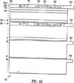
本発明の別の局面を例示するために、図26は、左側に、フラッシュメモリ装置の幾つかのブロックの内容例(これは、図24に示される情報と同じである)を示し、右側に、図の左側にあるブロック情報に対応するテーブル700の内容例を示す。ブロックの内容を示す目的は、単に、テーブル700に関するブロックのLBA−PBAアドレッシング間の相関性を理解する際の読み手に対する便宜を図るためである。図26に示される例は、フラッシュメモリ中に格納される際のブロックのアドレスと、情報がSPM RAMブロック548に格納される場合と同じブロックのアドレスとの間のこの代替の実施形態のマッピングを例示するものである。テーブル700では、1列に、各行毎に、仮想PBAフィールド1036と、欠陥フラグ1012を含むフラグフィールド1038とが格納されて示されている。行1040、1042、1044、...、1050は、それぞれLBAに対応し、それぞれ「0」、「1」、「2」、...「Z」によってアドレッシングされる。各行毎の仮想PBAフィールド1036は、実際には、内部に格納された16のセクタを有するフラッシュメモリ内のブロックを指すLBAアドレスポインタを含む。この点では、仮想PBAが、16セクタのPBAとして機能する(セクタの数は、代替の実施形態では、16以外でもよい)。
ホストが、例えばLBA05を読取るコマンドを送ると、図10におけるコントローラ506が、先ず、値「00」を得るために、値「05」の4つの最下位ビット(LSB)を生成する。次に、「00」をテーブル700の行アドレスとして用いて、図26の行1040がアドレッシングされる。ホストによって送られるLBA値の4つのLSBがマスクされる理由は、テーブル700の各行によって表される16のセクタが存在するからであることに留意されたい。16のセクタは、2値表記では4ビットに変換される2の4乗である。例えば、各行が32のセクタを表す場合には、ホストによって送られるLBAの5つのLSBがマスクされる。
SPM RAMブロック548中の行1040がアドレッシングされると、行1040に関する仮想PBAフィールド1036の値(この場合「00」である)が取出され、「00」が次に、フラッシュメモリ装置内に格納されるブロックに対するポインタとして使用される。つまり、この例においては、ブロック0またはブロック1000(図26の左側)がアドレッシングされる。しかし、読取りが意図されたセクタに到達するためには、ホストによって送られたLBA値から最初にマスクされた4ビットが、ブロック1040内の6番目のセクタであるセクタ「5」(不図示)を具体的にアドレッシングするために使用される。セクタ5(不図示)のデータフィールド1052に格納されたデータは、次に、取出される、または読取られる。次に、同じセクタのECCフィールド1014が読取られる。
LBAロケーション1020は、テーブル700の行1040の仮想PBAフィールド1036に格納されるのと同じアドレス値である値「00」を有するべきである。これは、スペースマネージャを更新するために、パワーアップルーチン間に、フラッシュメモリ装置においてブロック1000をブロック「00」として識別することを意図する。しかし、LBAロケーション1020は、上記のようにホストによって送られるLBA値を表さない。このような混乱を避けるために、ロケーション1020の値は、LBAアドレスではなく、「クラスタ」アドレスと呼ばれ得る。
書込み動作の状況における別の例を例示するために、ホストが、コントローラ506に対してLBA「17」(10進数)に書込みを行うことを命令すると、コントローラは、「17」の16進数(すなわち、「11」)のLSBをマスクする。「17」のマスクされたバージョンは、16進数で「1」である。従って、行1042が、テーブル700においてアドレッシングされ、スペースマネージャブロック544によって見つけられるようなフリーブロックのアドレスが、行1042の仮想PBAフィールド1036に配置される。この場合には、ブロック2が、次のフリーブロックとして見つけられる。フラッシュメモリ装置内で、ブロック1002であるブロック2がアドレッシングされる。情報が実際に書込まれるセクタは、ブロック1002のセクタ1(該ブロック中の第2のセクタ)である。なぜなら、LBA値「11」の4つのLSBがホストによって送られるからである。データおよびECCは、次に、ブロック1002のセクタ1に書込まれる。
図26の好適な実施形態例が、図25を参照して説明された実施形態と共に使用される場合には、LBA(またはクラスタ)アドレスが、各ブロック内の2つの場所に書込まれる。
本発明を具体的な実施形態の面から説明したが、それらの変更および改変が、当業者には無論明らかとなることが予想される。従って、以下の請求の範囲が、本発明の真の精神および範囲に入るような、そのような変更および改変の全てを包含するものとして解釈されることを意図する。Background of the Invention
Citation of related application
This application is a continuation-in-part of my earlier application No. 08 / 509,706, filed July 31, 1995, entitled “Direct Logical Block Addressing Flash Memory Mass Storage Architecture”.
Field of Invention
The present invention relates to the field of mass storage of computers. In particular, the present invention relates to an architecture for replacing a hard disk with a semiconductor non-volatile memory and in particular a flash memory.
Computers traditionally use rotating magnetic media for mass storage of documents, data, programs and information. However, this type of hard disk drive, which is widely used and generally accepted, suffers from various drawbacks. Because the disk rotates, there is a specific latency when extracting information from the hard disk drive.
Another problem is particularly noticeable in portable computers. In particular, the hard disk cannot withstand many of the various physical shocks that a portable computer is likely to receive. In addition, rotating disk motors consume significant power and reduce the battery life of portable computers.
A semiconductor memory is an ideal choice for replacing a mass storage hard disk drive because it can solve the above problems. Possible solutions have been proposed for replacing hard disks with semiconductor memory. In order to make such a system really easy to use, the memory must be non-volatile and changeable. The inventors have determined that flash memory is preferred for such replacement.
A flash memory is a transistor memory cell that can be programmed by hot electrons, source injection, tunneling, and erasable by Fowler-Nordheim tunneling. Programming and erasing of such memory cells requires current to pass through the dielectric surrounding the floating gate electrode. Thus, this type of memory has a finite number of erase-write cycles. Eventually the dielectric deteriorates. Flash cell device manufacturers specify a limit on the number of erase-write cycles between 100,000 and 1,000,000.
One of the conditions for successful operation of semiconductor mass storage devices is to make it clear to designers and users of systems that use such devices how to use them instead of rotating media hard disk mass storage devices. In other words, a designer or user of a computer incorporating such a semiconductor mass storage device can easily remove the hard disk and replace it with a semiconductor mass storage device. All commercially available software currently available should operate in a system utilizing such a semiconductor mass storage device without any modification.
SanDisk proposed an architecture for semiconductor mass storage using flash memory at the Silicon Valley PC Design Conference on July 9, 1991. This mass storage system includes a 512 byte read / write block size corresponding to the sector size of a commercially available hard disk.
So far, the design (Figure) has built in a pre-write erase architecture. In order to update the media file in this process, if the physical location on the media was previously programmed, it must be erased before new data can be reprogrammed.
This process has a significant adverse effect on the overall throughput of the system. When the host writes a new data file to the storage medium, the host provides a logical block address to the peripheral storage device associated with the data file. The storage device then converts this given logical block address to the actual physical block address on the medium and performs the write process. In a magnetic hard disk drive, new data is overwritten with old data without changing the medium. Thus, once the physical block address is calculated from the given logical block address from the controller, the data file is simply written to that location. In a semiconductor memory device, if the location corresponding to the calculated physical block address was previously programmed, it must be erased before this block is reprogrammed with new data. In one prior art, in a pre-write erase architecture, the correlation between logical block addresses provided by the host is a one-to-one mapping to physical block addresses on the medium. This method has many drawbacks. First, performance is slow due to the erasure process before reprogramming the changed information. In semiconductor flash, erasing is a very slow process.
Next, hard disk users typically store two types of information. One is information that is rarely modified, and the other is information that changes frequently. For example, commercially available spreadsheets or word processing software programs stored in the user's system rarely change, if any. However, spreadsheet data files or word processing documents are frequently changed. In this way, each sector of the hard disk is typically used in a completely different way in terms of the number of times the information stored therein is changed. This difference does not affect the hard disk at all because it is not sensitive to data changes, but in flash memory devices this part of the mass storage device is exhausted much faster than other parts of the mass storage device. And cannot be used.
In another architecture, the inventors have previously proposed a solution to store a table that correlates logical block addresses to physical block addresses. Inventions relating to the solution are disclosed in US Patent Application No. 08 / 038,668 filed on March 26, 1993 and US Patent Application No. 08 / 037,893 filed on March 26, 1993. These applications are incorporated herein by reference.
The inventor's conventional solution discloses two main algorithms and the hardware architecture associated with the semiconductor mass storage device. As used herein, “data file” is understood to mean any computer file including commercially available software, user programs, word processing software documents, spreadsheet files, and the like. The first algorithm in the conventional solution provides means for avoiding erasure processing when a modified data file is written back to the mass storage device. In other words, a data file that has not been erased and has been modified is written to an empty part of the large capacity device.
The semiconductor mass storage device architecture has blocks having a size corresponding to the sector size of a commercially available hard disk. Each block can be erased. In some embodiments, such replacement is apparent because the semiconductor mass storage device can replace a rotating hard disk without affecting the user. Means are provided for preventing the information stored in the mass storage device from being changed at each point of the pre-write erase cycle.
According to the first algorithm, the erase cycle is avoided by programming the modified data file into an empty block. This is usually not possible when using conventional mass storage devices. This is because the central processing unit and commercially available software used in conventional computer systems are not configured to keep track of the changing physical location of the data file. Conventional solutions include a programmable map to maintain the correlation between the logical and physical addresses of the updated information file.
All flags and a table that correlates logical block addresses to physical block addresses are maintained within the array of CAM cells. The use of a CAM cell determines the desired physical address in the mass storage device very quickly, usually within one or two clock cycles. Unfortunately, as is well known, a CAM cell typically requires six multiple transistors. Therefore, an integrated circuit that constitutes a memory of a specific size using a CAM storage device for tables and flags needs to be much larger than a circuit that simply uses other means for storing the memory. .
The inventors have proposed another solution to this problem, which is disclosed in US patent application Ser. No. 08 / 131,495, filed Oct. 4, 1993. This application is incorporated herein by reference.
Another conventional solution invented by these same inventors is also for non-volatile memory storage devices. The device is also configured not to perform pre-write erasure every time the data file is changed by maintaining the correlation between the logical block address and the physical block address in the non-volatile space manager RAM. Furthermore, the present invention avoids the overhead associated with the CAM cell approach that requires additional circuitry.
Like the solution previously disclosed by these same inventors, the device includes two major algorithm implementations and circuitry for the hardware architecture associated with the semiconductor mass storage device. In addition, CAM cells can avoid conventional solutions by using RAM cells.
In this conventional solution for providing a logical block address to a memory storage device, a read is performed. The system compares the sequentially stored logical block addresses until a match is found. The data file is then incorporated into the digital system. Thus, this solution degrades performance because all memory locations are potentially retrieved and compared to the desired logical block address before the physical location of the desired information is determined.
What is needed is a semiconductor hard disk architecture that provides rapid access to stored data without the excessive overhead of CAM cell equipment.
Summary of the Invention
The present invention is for a non-volatile memory storage device. The apparatus is configured not to perform pre-write erasure every time a data file is changed. Furthermore, in order to avoid the overhead associated with CAM cells, the present technique utilizes a RAM array. The host system uses the logical block address to maintain the mass storage data organization. The RAM array is configured to be addressed by the same address as the host logical block address (LBA). Each location so addressed in the RAM includes a field that holds the physical address of the data in the non-volatile mass storage device sought from the host. This physical block address (PBA) information must be held in a non-volatile memory that ensures that the device still functions after resuming processing after a power failure. This is because RAM is a volatile memory. In addition, status flags are also stored at each physical location. The status flag can be stored either in a non-volatile medium or in both RAM and non-volatile medium.
The device has a circuit configuration for the execution of two main algorithms and a hardware architecture associated with the semiconductor mass storage device. The first algorithm provides a means of mapping host logical blocks to physical block addresses, which significantly improves performance and requires minimal hardware assistance. In addition, the second algorithm provides a means for avoiding a pre-write erase cycle when the modified data file is written back to the mass storage device. Instead, no erasure is performed and the modified data file is written to an empty part of the mass storage device.
In the present invention, reading is performed by providing a logical block address to the memory storage device. The RAM array is configured such that a logical block address selects one RAM location. The location holds the physical block address of the data requested from the host or other external system. The data file is then read to the host. In the second algorithm, the erase cycle is avoided by programming the modified data file into the modified data mass storage block rather than programming itself after the block erase cycle as done in the prior art. Is done.
In another embodiment of the present invention, the method and apparatus efficiently moves a sector in a block from a first region within a non-volatile memory to an unused region within the non-volatile memory, and the first region is “in use”. It is presented to be marked as “.
That is, the preferred embodiment of the present invention stores mapping information for mapping a logical block address that identifies a block accessed by a host to a physical block address, and is a non-volatile memory that can be selectively erased and moved individually. And a method and apparatus for identifying a block having one or more sectors. The mapping information includes a virtual physical block address that identifies the “original” location in the non-volatile memory and a moved virtual physical block address that identifies the “moved” location in the non-volatile memory, Blocks are stored inside the former, and sectors of one or more stored blocks are moved inside the latter. The mapping information further includes status information for using the “original” physical block address, and “moved” physical block address for providing information about the “moved” sector within the accessed block. include.
Figure
FIG. 1 shows a schematic block diagram of an architecture for a semiconductor mass storage device according to the present invention.
FIG. 2 illustrates another embodiment of the
FIG. 3 shows a block diagram of a system incorporating the mass storage device of the present invention.
FIGS. 4-8 illustrate several flags and information states for realizing the advantages of the present invention.
FIG. 9 shows a flowchart block diagram of a first algorithm relating to the present invention.
FIG. 10 shows a high-level block diagram of a digital system such as a digital camera that includes a preferred embodiment of the present invention.
FIGS. 11 to 21 show some examples showing the state of a mapping table that may be stored in the digital system of FIG. 10 including LBA-PBA mapping information.
FIG. 22 shows an example of a non-volatile memory device used in the preferred embodiment of FIG.
FIG. 23 shows a high-order flowchart showing the general steps used to write a block of information to the non-volatile device of FIG.
FIG. 24 is an example of the contents of a flash memory device in another embodiment of the present invention using a new defect flag and LBA address means.
FIG. 25 is an example of the contents of a flash memory device used in another alternative embodiment of the present invention that stores an LBA address for each block at two different sector locations within the block.
FIG. 26, keyed in FIG. 26b, includes FIGS. 26a and 26b, and shows another alternative example embodiment of the present invention. There, the contents of the flash memory device and the SPM RAM block are described, showing the interrelationship between LBA and PBA addressing as used in the system of FIG.
Detailed Description of the Preferred Embodiment
FIG. 1 shows an architecture for implementing a semiconductor storage medium according to the present invention. The storage medium is for use with a host or other external digital system. The mass storage device is divided into two parts, a
The
There are a plurality of
The physical block address (PBA) can be divided into two fields as shown in FIG. These fields can be used for the cluster address of a group of data blocks. The
A collection of information flags is also stored for each
When writing data to the mass storage device of the present invention, the controller determines a first available physical block for storing the data. The
Consider an example where a user prepares a word processing document and instructs the computer to save the document. Documents are stored in a mass storage system. The host system assigns a logical block address to the mass storage system. The mass storage system of the present invention selects a physical address of an unused block or a block in the mass storage device for storing a document. The address of the physical block address is stored in the
Assume further that the user retrieves the document, makes changes, and gives the computer instructions to store the document again. To avoid a pre-write erase cycle, the system of the present invention locates a block with an in-use /
Since the
In order to assign the latest physical block address assigned to the logical block address in the
FIG. 3 shows a block diagram of a system incorporating the mass storage device of the present invention. An external
Simplified examples showing the operation of the writing process according to the present invention are shown in FIGS. All information flags are not shown so as not to obscure features of the invention due to excessive explanation. Data entries are shown in decimal numbers to further simplify the understanding of the present invention. It will be apparent to those skilled in the art that in the preferred embodiment, binary is used.
FIG. 4 shows a mass storage device with eleven entries relating to the present invention. No valid or usable data is stored in the mass storage device of FIG. Therefore, all physical block addresses are empty. The data stored at location '6' of the non-volatile mass storage device is clogged and outdated. Furthermore, location '9' is defective and cannot be used.
As an example of the mass storage device, the host instructs the logical block address '3' and then '4' to sequentially write data. The mass storage device first writes data associated with logical block address '3'. The device determines the first unused location in non-volatile memory. In this example, the first free location is location '0'.
Therefore, FIG. 5 shows that the physical block address “0” corresponding to the logical block address “3” is stored, and the in-use flag is set to the physical block address “0”. The next available place is location '1'. FIG. 6 shows that the physical block address “1” corresponding to the logical block address “4” is stored, and the in-use flag is set to the physical block address “1”.
The host instructs to write something again to the logical block address '3'. The next vacant place is determined to be location '2'. In FIG. 7, location '0' is shown to indicate that the data is no longer available, the busy flag is set to location '2', and the physical block address at location '3' has been changed to '2'. Indicates that the old flag in 'is set.
Further, the host instructs to write something again to the logical block address “4”. The next available place is determined to be location '3'. In FIG. 8, location '1' is shown to indicate that the data is no longer available, the busy flag is set to location '3', and the physical block address at location '4' has been changed to '3'. 'Indicates that the old flag is set. (Recall that there is generally no relationship between physical block addresses and data stored at the same location).
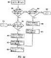
FIG. 9 shows
On the other hand, if the system cannot find a block with a used / free flag that is not set, the system will use the flag (used / free and old / new) and data for all blocks with the old / new flag set. Then, the defect flag that has not been set is erased (step 204), and a block having an unset in-use / free flag is searched (step 202). Such a block is only generated by
If the data is a modified version of a file that exists so far, the system must prevent the swapped version from being accessed. The system determines whether the data file replaces the old data file (step 208). If so, the system sets the old / new flag associated with the replaced block (step 210). On the other hand, if the stored data file is a newly created data file, the old / new flag setting step (step 210) is skipped because there is no block to be replaced. Finally, the map correlating logical address 308- with the physical address is updated (step 212).
In accordance with the procedure outlined so far, overhead associated with an erase cycle is avoided for each write to
In the preferred embodiment of the present invention, programming of the flash memory follows a procedure commonly known by those skilled in the art. In other words, the program's impulse is applied to properly program the bits, and the programmed data is compared to confirm that proper programming has been performed. Eventually the bits are not erased or programmed correctly and the defect flag 148 is set so that the block is not used again.
FIG. 10 shows a
The illustrated
The illustrated
The
The space manager block 544 uses a suitable apparatus and algorithm to find the next unused (or free) storage block in one flash memory device for storing one block of information. This will be further described herein with reference to other figures. As already explained, the address of one block in one flash memory device is called PBA, which is determined by the space manager by performing a translation on the LBA received from the host. Various devices and methods can be used to accomplish this translation. An example of such a scheme is disclosed in US Pat. No. 5,485,595, entitled “Flash Memory Mass Storage Architecture Incorporating Wear Leveling Technique Without Using CAM Cells”, the specification of which is incorporated herein by reference. Incorporate. Other LBA to PBA translation methods and apparatus may be used as well without departing from the scope and spirit of the present invention.
The space manager block 544 includes an
In operation, the
Under the direction of the
Referring to FIG. 10,
Note that the
If one or more sectors have been moved from one area of flash memory to another, the preferred embodiment of the present invention first stores the sectors in the flash memory device, ie 510-512. From the location being moved to the
FIGS. 11-21 illustrate example states of a table 700 in the
The rows of the table include PBA /
In the preferred embodiment, each block is shown to include 16 sectors. This is due to the ability to selectively erase the entire block of 16 sectors. (For this reason, the block size may be referred to as “erase block size”.) As shown in FIGS. 11 to 21, when the erase block size is 16 sectors, each block entry (or row) has 16 Contains information about sectors. Thus,
However, it should be noted that other block sizes may be used as well. For example, a block includes 32 sectors, and thus may include an erase block size of 32. In the latter situation, 716, 718, 720. . . Etc., each block entry or row contains information about 32 sectors, where each block consists of 16 sectors. (Sizes other than the 16 sector block size may be used as well.)
The VPBA
Sector
Still referring to FIG. 11, by way of example, an example status of table 700 stored in SPM RAM block 548 (FIG. 10) when LBA “0” is written is shown. As already mentioned, in the drawings presented herein, the block size consisting of 16 sectors (0-15 in decimal or 0-10 in hexadecimal) is for illustrative purposes only. Used for. Similarly, N blocks (and thus N LBAs) are used and given numbers from 0 to N-1. The block size and number of blocks are design choices that can vary for different applications and can depend on the memory capacity of each of the separate flash memory devices being used (such as 510-512). Furthermore, although a preferred sector size of 512 bytes is used in these embodiments, other sector sizes may be used without departing from the scope and spirit of the present invention.
When all the blocks in the
A value of 734 is in a logical state “0”, indicating that the LBA “0” block does not contain any moved sectors.
In FIG. 11, for all remaining rows 716-728 of table 700, rows such as
At this time, a description of the content of one of the flash memory devices in the
Referring now to FIG. 22, an example of the contents of
The
From the description of the present embodiment provided herein, the information in the PBA row of the
That is, rather than reading all PBA rows (16 total rows in the preferred embodiment) and updating each LBA entry in table 700 at power-up, only the first PBA row for each LBA is read from flash memory. And need to be stored in the
In the above embodiment where
In the
Continuing the above example, FIG. 12 shows an example of the state of the table 700 when LBA0 is written again by the host. Since LBA0 has already been written and is written again without first being erased, another free location in
The entry in
Referring now to FIG. 22, the state of the table 700 in FIG. 12 is that the moved sector of the LBA “0” block is now written to the PBA “10” in
Although not specifically shown in the drawing, the move flag in
FIG. 13 shows the status of the table 700 when another write operation to the LBA “00” is executed. The value (or entry) in
Continuing with the above example, FIG. 14 shows the state of table 700 when yet another write to LBA “0” is performed. In order to facilitate comparison, the values shown in FIG. 14 that are in different logical states with respect to the state shown in FIG. 13 are circled. All remain the same except for the newly moved location, shown as PBA “30”, shown in
Row 718 remains the same until erased. The flags in
FIG. 15 is another example of the state of the table 700. The table 700 is a state in which it is assumed that the table is in the state shown in FIG. 13, and that writing to the host LBA “5” follows. Indicates. Again, from FIG. 13 to FIG. 15, the change to the value in the table 700, which is a one-time change, is shown by enclosing the changed value in a circle.
When writing to LBA “5”, the LBA entries in
FIGS. 16-18 illustrate yet another example of how the state of the table 700 can be after either power-up or erasure of a block by the
FIG. 18 shows the state of the table 700 after picking up after FIG. 17 and the host writing to LBA “5”. As shown in FIG. 18, LBA “5” is moved to PBA “10”. Here, LBA “0” is also placed in PBA “10”. For this purpose, the MBPBA
18 will be described. FIG. 19 shows the state of the table 700 after the host has written another time into the LBA “0”. According to the table, yet another free PBA location “20” is found where LBA “5” and LBA “0” have moved. First, LBA “5” moves to location PBA “10”, location PBA “20”, and then a new block of location LBA “0” is written to PBA “20”. As previously described, first, a block move is performed (eg, where the block with LBA “5” is moved) at any time within the
The used flag in
FIG. 20 shows yet another state of what the table 700 could be after picking up from the state of table 700 shown in FIG. 18 and the host writing to LBA “5”. In this case, the block of LBA “0” first moves from the currently stored location PBA “10” in the
FIG. 21 also shows the state of what the table 700 could look like after picking up from the state of the table 700 shown in FIG. 18 and writing to LBA “7” by the host. In this case, the location is not yet used, so a new block is simply written to location PBA “10” in the flash memory. In addition, the three bits of
As can be understood from the discussion presented so far, at some point the number of sectors moving within a block facilitates inefficient operation. Thus, within a block, the user is marked as "old" (the old flag is set) and the block is erased with a threshold on the number of sectors that can be moved before the block is no longer used It is necessary to set up to. This threshold value may be set to, for example, half the number of sectors in one block. This is shown as follows. In the case of one block having 16 sectors, 8 sectors are moved to another block, and the “original” block and the “moved” block (the block where the moved sector exists) are the same PBA. Combined into blocks. The combined PBA block may be stored in a new block as a whole, or the “original” block is combined with the “moved” block and moved into the “moved” block. Also good. In the latter case, the “original” block is then marked “old” for its erasure. If the combined PBA block is stored in a new block, both the “original” block and the “moved” block are marked “old”.
FIG. 23 shows a summary flowchart that outlines some of the steps performed during a write operation. This is intended to show some sequence of events that occur during such operation, and is in no way an exhaustive presentation of the method or apparatus used in the preferred embodiment of the present invention.
The steps as outlined in FIG. 23 are performed under the direction of the
Returning to step 802, if an LBAM block is in use, a search for the next free PBA block is also performed at
Finally, after
As noted above, if a significant portion of a block has moved sectors (in the preferred embodiment, this is 8 out of 16 sectors), this block has a corresponding “old” It is indicated as “old” by setting a flag. Periodically, blocks with the “old” flag set can be erased and then reused (or reprogrammed or rewritten).
As can be appreciated, an advantage of the embodiment of FIGS. 10-23 is that blocks need not be erased each time they are accessed by the host. For example, if any part (or sector) of a block is being rewritten, the block is erased in the flash memory device, or the entire block is moved to a free area in the flash. Instead, only the part being rewritten needs to be moved to another location in the flash (ie, a free location identified by the MVPA block address). In this connection, time-consuming erase cycles are avoided until later, and no time is wasted reading the entire block and moving the entire block.
In alternative embodiments, less information may be associated with each sector stored in the flash memory. Similarly, table 700 in SPM RAM block 548 (FIG. 10) maintains less information, as will be described below.
FIG. 24 shows an example of information that can be stored in a flash memory chip (such as the flash memory device 510). FIG. 24 shows N blocks (
The first sector in each block (eg,
Each sector in one block may further include a
Similarly, the location of the
During the manufacture of flash memory chips, defects in the memory are typically identified and marked by the chip manufacturer. This is typically done by writing a predefined pattern (byte width) at a predetermined location within the defective block. That is, the manufacturer erases the flash chip and all values such as “1” are then retained by each memory cell in the successfully erased flash chip. If the sector or cell in the block is a defective product, the manufacturer sets a manufacturing defect flag arranged somewhere in the defective block (not shown in FIG. 24) to a predetermined value. This manufacturing defect flag is different from the
In addition to defects detected during the manufacture of flash chips, there may be additional defects that progress during chip operation due to wear, as explained above. These defects are sometimes referred to as “grown defects” throughout the industry and must be considered by the system in which the use of flash memory devices is used.
The case of “growth defects” is explained in terms of system operation. In the preferred embodiment of the present invention, after erasing
The use of the
If one or more cells in one block fail during the write operation, the block is first erased, and then the
One advantage of having a defect flag as previously described is that the space manager block 544 (FIG. 10) can quickly find non-defective blocks during system power-up. .
In an alternative embodiment, as shown in FIG. 25, the LBA of each block in the flash memory device is stored in two different sectors of the same block. For example, after
Thereafter, whenever power to the system is temporarily interrupted or upon power up, the two LBAs at
As shown in FIG. 24, when only one LBA is used for each block, obviously two LBAs in each block are not compared, but detection of a defective block is not , As described above, maintained by the use of a defect flag. Further, the LBA may be written last (ie, after all sectors of the block have been written). Writing the LBA last is an additional indication that you have successfully written to the block.
To illustrate another aspect of the present invention, FIG. 26 shows on the left side an example of the contents of several blocks of a flash memory device (this is the same as the information shown in FIG. 24), and on the right side The example of the content of the table 700 corresponding to the block information on the left side of the figure is shown. The purpose of showing the contents of the block is merely for the convenience of the reader in understanding the correlation between the LBA-PBA addressing of the block with respect to the table 700. The example shown in FIG. 26 illustrates the mapping of this alternative embodiment between the address of the block as it is stored in flash memory and the address of the same block as when the information is stored in
When the host sends a command to read LBA05, for example, the
When
The
To illustrate another example in the context of a write operation, when the host commands the
When the preferred embodiment example of FIG. 26 is used with the embodiment described with reference to FIG. 25, the LBA (or cluster) addresses are written to two locations within each block.
Although the present invention has been described in terms of specific embodiments, it is expected that changes and modifications will become apparent to those skilled in the art. Accordingly, it is intended that the following claims be interpreted to embrace all such changes and modifications as fall within the true spirit and scope of the present invention.
Claims (59)
Translated fromJapanese該格納装置は、
(a)n個のLBA行によって規定されるテーブルを格納するメモリ装置であって、該n個のLBA行の各々は、LBAによって一意的にアドレス可能であり、該メモリ装置は、該格納されたブロックのロケーションを識別する仮想PBAと、該格納されたブロックの一部のロケーションを識別する移動仮想PBAと、該格納されたブロックのいずれかのセクタが該不揮発性メモリ内の該移動仮想PBAのロケーションに移動されたか否かを示すフラグ手段を含むステータス情報とを格納する、メモリ装置と、
(b)該不揮発性メモリ内に格納されるべき、特定のLBAによって識別される情報のブロックを該ホストから受け取り、該特定のLBAが「未使用」場合には、該仮想PBAを変更し、該特定のLBAが「使用中」である場合には、該移動仮想PBAを変更する手段と
を備え、
該ホストが該格納装置に書込みを行う毎に消去動作を行うことを回避するように、かつ、ブロックの一部が再書込みされる毎に該不揮発性メモリ内のフリーロケーションにブロック全体の転送を回避するように、該ブロックの一部が該不揮発性メモリ内のロケーションであって1つより多いPBAによって識別されたロケーションに格納され得る、格納装置。A storage device having a nonvolatile memory and connected to a host, wherein the storage device stores information composed of a plurality of blocks in the nonvolatile memory, and each block has a logical block address ( LBA) and a physical block address (PBA), the LBA is provided by the host to the storage device to identify the block to be accessed, and the PBA Areprovided by the storage device to identify free locations in the non-volatile memory to be stored, each stored block in the non-volatile memory being selectively erasable, and 1 Further comprising one or more sectors,
The storage device
(A) A memory device that stores a table defined by n LBA rows, each of the n LBA rows is uniquely addressable by an LBA, and the memory device is stored in the memory device A virtual PBA identifying the location of the stored block, a moving virtual PBA identifying the location of a portion of the stored block, and any sector of the stored block is the moving virtual PBA in the non-volatile memory A memory device for storing status information including flag means indicating whether the location has been moved to,
(B) receiving from the host a block of information identified by a specific LBA to be stored in the non-volatile memory, and if the specific LBA is “unused”,change the virtual PBA; Means forchanging the mobile virtual PBA when the specific LBA is “in use”;
The entire block is transferred to a free location in the non-volatile memory so as to avoid erasure operation every time the host writes to the storage device, and each time a part of the block is rewritten. A storage device, wherein a portion of the block may be stored at a location in the non-volatile memory and identified by more than one PBA to avoid.
該方法は、
(a)該コントローラ内に、複数の行によって規定されるテーブルを割り当てることであって、各行は、LBAによって個別にアドレス可能であり、仮想PBAと、移動仮想PBAと、該フラッシュメモリ装置内の該仮想PBAから該移動仮想PBAに移動されたセクタのロケーションを決定する際に用いられるステータス情報とを格納するように構成されている、ことと、
(b)該ホストによってアクセスされているブロックを識別する特定のLBAを該コントローラに提供することと、
(c)該特定のLBAに関連してPBAを選択することと、
(d)LBA行をアドレス指定するように該特定のLBAを用いることと、
(e)該アドレス指定されたLBA行に該特定のLBAに関連付けられた該PBAを格納することと、
(f)該特定のLBAによって識別された該ブロックへのさらなるアクセスの際に、移動仮想PBAを選択することと、
(g)該アドレス指定されたLBA行に該移動仮想PBAを格納することと、
(h)該アドレス指定されたLBA行内のいずれかのセクタが移動されたか否かを示すように、該アドレス指定されたLBA行のステータス情報を変更することと
を包含し、
ブロックがアクセスされる度に書込み前の消去動作を回避するように、該ブロックのセクタが該フラッシュメモリ装置内の使用されていないロケーションに移動される、方法。A storage device used with a host and having a controller and one or more flash memory devices, wherein the information in the one or more flash memory devices is accessed under the direction of the controller, comprising: Consists of a plurality of sectors, wherein one or more sectors define a block, each block being selectively erasable and used within the flash memory device in which the sector can be stored Associated with alogical block address ( LBA) provided by the host and aphysical block address ( PBA)provided by the controller to identify a location that has not been
The method
(A) Allocating a table defined by a plurality of rows in the controller, each row being individually addressable by an LBA, a virtual PBA, a moving virtual PBA, and a flash memory device Configured to store status information used in determining a location of a sector moved from the virtual PBA to the mobile virtual PBA;
(B) providing the controller with a specific LBA identifying the block being accessed by the host;
(C)selecting a PBA in relation to the particular LBA;
(D) using the specific LBA to address the LBA row;
(E) storing the PBA associated with the particular LBA in the addressed LBA row;
(F) when further access to the block identified by the particular LBA, andselecting a mobile virtual PBA,
(G) storing the mobile virtual PBA in the addressed LBA row;
(H) changing the status information of the addressed LBA row to indicate whether any sector in the addressed LBA row has been moved,
A method wherein a sector of the block is moved to an unused location in the flash memory device so as to avoid an erase operation before writing each time the block is accessed.
該格納装置は、
n個のLBA行によって規定されるテーブルを格納するメモリ装置であって、該n個のLBA行の各々は、LBAによって一意的にアドレス可能であり、該メモリ装置は、該格納されたブロックのロケーションを識別する仮想PBAと、該格納されたブロックの一部のロケーションを識別する移動仮想PBAと、該格納されたブロックのいずれかのセクタが該不揮発性メモリ内の該移動仮想PBAのロケーションに移動されたか否かを示すフラグ手段を含むステータス情報とを格納する、メモリ装置と、
該不揮発性メモリ内に格納されるべき、特定のLBAによって識別される情報のブロックを該ホストから受け取り、該特定のLBAが「未使用」場合には、該仮想PBAを変更し、該特定のLBAが「使用中」である場合には、該移動仮想PBAを変更する手段と
を備え、
「欠陥」フラグは、該複数のブロックの各々に格納されており、成功裏に消去されたブロックを識別するように、所定の値に設定されており、
該ホストが該格納装置に書込みを行う毎に消去動作を行うことを回避するように、かつ、ブロックの一部が再書込みされる毎に該不揮発性メモリ内のフリーロケーションにブロック全体の転送を回避するように、該ブロックの一部が該不揮発性メモリ内のロケーションであって1つより多いPBAによって識別されたロケーションに格納され得る、格納装置。A storage device having a nonvolatile memory and connected to a host, wherein the storage device stores information composed of a plurality of blocks in the nonvolatile memory, and each block has a logical block address ( LBA) and a physical block address (PBA), the LBA is provided by the host to the storage device to identify the block to be accessed, and the PBA Areprovided by the storage device to identify free locations in the non-volatile memory to be stored, each stored block in the non-volatile memory being selectively erasable, and 1 Further comprising one or more sectors,
The storage device
A memory device that stores a table defined by n LBA rows, each of the n LBA rows is uniquely addressable by an LBA, and the memory device stores the stored block's A virtual PBA identifying a location, a moving virtual PBA identifying a location of a portion of the stored block, and any sector of the stored block at the location of the moving virtual PBA in the non-volatile memory A memory device for storing status information including flag means indicating whether or not moved;
Receive from the host a block of information identified by a particular LBA to be stored in the non-volatile memory, and if the particular LBA is "unused",modify the virtual PBA and Means forchanging the migration virtual PBA when the LBA is “in use”;
A “defect” flag is stored in each of the plurality of blocks and is set to a predetermined value to identify a successfully erased block;
The entire block is transferred to a free location in the non-volatile memory so as to avoid erasure operation every time the host writes to the storage device, and each time a part of the block is rewritten. A storage device, wherein a portion of the block may be stored at a location in the non-volatile memory and identified by more than one PBA to avoid.
複数の格納サイトを含むテーブルを格納する揮発性メモリであって、該複数の格納サイトの各々が特定のLBAによってアドレス可能であり、特定のPBAに関連付けられた該複数の格納サイトの各々は、特定のLBAに対応する情報が該特定のブロックの複数の行のうちの1つ以上に格納されている、または、格納されるべき該不揮発性メモリ内の特定のブロックを識別する、揮発性メモリと、
該メモリ装置に関連付けられたコントローラであって、ホストからの対応するLBAの受け取りに応答して、特定のPBAによって識別された該不揮発性メモリ内のブロックにアクセスし、該コントローラは、特定のPBAの少なくとも一部にアクセスすることにより、該アクセスされたブロックからデータを読み出すか、または、該アクセスされたブロックにデータを書き込むように動作し、該コントローラは、該アクセスされたブロック内の2つの異なるロケーションに該対応するLBAを書き込むようにプログラムされており、データが格納された任意のブロックにアクセスすると、該コントローラは、該ブロック内の該2つの異なるロケーションに書き込まれたLBAを比較し、該LBAが整合した場合には、情報格納のために該ブロックを使用し、該LBAが整合しなかった場合には、再使用に先立って該ブロックを消去するように動作可能である、コントローラと
を備えた、格納装置。A non-volatile memory configured to be coupled to a host processor, the non-volatile memory storing information identified by a logical block address (LBA) assigned by the host processor, the non-volatile memory is composed of a plurality of blocks of a plurality of rows numberedfor storingsaid information, each block is identified by a physical block address (PBA), and non-volatile memory,
Avolatile memory storing a table including a plurality of storage sites, each of the plurality of storage sites being addressable by a specific LBA, and each of the plurality of storage sites associated with a specific PBA is Volatile memory in which information corresponding to a particular LBA is stored in one or more of the rows of the particular block, or identifies a particular block within the non-volatile memory to be stored When,
A controller associated with the memory device, in response to receiving a corresponding LBA from a host, accessing a block in the non-volatile memory identified by a particular PBA; of by accessingat leasta portion, or reads data from the accessed block, or operates to write data to the accessed block, the controller, the two of the accessed block When programmedto write thecorresponding LBAto different locations and accessing any block where data is stored, the controller compares the LBA written to the two different locations within the block; If the LBA matches, the block is stored for information storage. Using the click, if the LBA is not matched is operable to erase the block prior to re-use, and a controller, storage device.
該方法は、
格納されるべき情報を受け取ることであって、該情報は、該ホストプロセッサによって割り当てられたLBAによって識別される、ことと、
特定のPBAによって識別された、該不揮発性メモリ内の利用可能なブロックであって、該情報を格納するために利用可能なブロックを決定することと、
特定のLBAによってアドレス可能な、該メモリ装置内のロケーションに該利用可能なブロックのPBAを格納することと、
該PBAによって識別された、該不揮発性メモリの該ブロック内に該情報を格納することと、
該ブロック内に「使用中」のフラグを設定することと、
該情報と共に、該ブロック内の第1のロケーションに該LBAを格納することと、
該ブロック内の第2のロケーションに該LBAを格納することと、
該格納装置の電源が投入される度に、該ブロックの該第1のロケーションに格納された該LBAと該ブロックの該第2のロケーションに格納された該LBAとを比較することと、
整合が見つかり、かつ、対応する「欠陥」フラグが設定されてない場合には、該データは、欠陥ではないと決定し、情報格納のために該ブロックを用いることを継続することと、
該ブロックの該第1のロケーションに格納された該LBAが、該ブロックの該第2のロケーションに格納された該LBAと整合せず、かつ、「欠陥」フラグが設定されてない場合には、該ブロックは、欠陥でないと決定し、該ブロックの一部が再使用される前に該ブロックを消去することと
を包含する、方法。A storage device comprising a controller, a non-volatile memory storing information identified by a logical block address (LBA) assigned by a host processor, and a memory device addressable by the controller, wherein the non-volatile memory comprises: The nonvolatile memory includes data and aset of flags, and the nonvolatile memory includes a plurality of blocks in a plurality of rows numberedfor storing information. At least a partof each blockis a physical block. Identified by an address (PBA), the memory device stores or should store the LBA and information corresponding to the specific LBA in one or more of the rows of the specific block Storing a table to convert to a corresponding PBA identifying a particular block in the non-volatile memory; Amethod of managing the storage of information in memory,
Themethod,
Receiving information to be stored, the information being identified by an LBA assigned by the host processor;
Determining an available block in the non-volatile memory identified by a particular PBA that is available to store the information;
Storing the PBA of the available block at a location in the memory device that is addressable by a particular LBA;
Storing the information in the block of the non-volatile memory identified by the PBA;
Setting a “in use” flag in the block;
Storing the LBA in a first location within the block along with the information;
Storing the LBA in a second location within the block;
Each time the storage device is powered on, comparing the LBA stored in the first location of the block with the LBA stored in the second location of the block;
If a match is found and the corresponding “defect” flag is not set, the data is determined not to be defective and continues to use the block for information storage;
If the LBA stored at the first location of the block does not match the LBA stored at the second location of the block and the “defect” flag is not set, the block includes a that decides not defective, to erase the block before the part of the block is reused,methods.
論理ブロックアドレス(LBA)によって識別された情報を受け取ることと、
該情報を格納するために、該不揮発性メモリ内の利用可能なブロックまたは該ブロックの一部を決定することであって、該利用可能なブロックまたは該ブロックの一部は、物理ブロックアドレス(PBA)によって識別される、ことと、
該LBAによってアドレス可能な、メモリ装置内のロケーションに該PBAを格納することと、
該PBAによって識別された、該不揮発性メモリの該ブロックまたは該ブロックの一部に該情報を格納することと、
「使用中」フラグを設定することと、
該ブロック内の第1のロケーションに該LBAを格納することと、
該ブロック内の第2のロケーションに該LBAを格納することと、
該格納装置の電源が投入される度に、
該第1のロケーションに格納された該LBAと該第2のロケーションに格納された該LBAとを比較し、整合が見つかり、かつ、「欠陥」フラグが設定されていない場合には、該データは、欠陥ではなく、情報格納のために該ブロックを続けて用いることを決定することと、
該第1のロケーションに格納された該LBAが該第2のロケーションに格納された該LBAと整合せず、かつ、「欠陥」フラグが設定されてない場合には、該ブロックは、欠陥でないと判定し、該ブロックの再使用の前に該ブロックを消去することを決定することと
を包含する、方法。Amethod for managing the storage of information in a storage device including a non-volatile memory so that defect data can be found quickly each time the storage device is turned on,
Receiving information identified by a logical block address (LBA);
To store the information, comprising: determininga portion of the available building block or the block of nonvolatile memory,a portion of the available building block or the block, a physical block address (PBA ) Identified by
Storing the PBA at a location in a memory device addressable by the LBA;
Storing the information in the block or partof the block of the non-volatile memory identified by the PBA;
Setting the “in use” flag;
Storing the LBA in a first location within the block;
Storing the LBA in a second location within the block;
Each time the enclosure is powered on
The LBA stored at the first location is compared with the LBA stored at the second location and if a match is found and the “defect” flag is not set, the data is Deciding to continue to use the block for information storage rather than defects;
If the LBA stored at the first location does not match the LBA stored at the second location and the“ defect” flag is not set, then the block is not defective judgment, including the decide to erase the blocks before re-use of the block,the method.
格納された情報ブロックに対する該マッピング情報は、
該格納された情報ブロックの本来の情報を格納する第1のブロックロケーションを示す第1の仮想PBAと、
該格納された情報ブロックの移動された部分を格納する第2のブロックロケーションを示す第2の仮想PBAであって、該移動された部分は、該格納された情報ブロックの再書き込みされた情報を含み、該本来の情報の対応する部分は、該移動された部分と取り替えられる、第2の仮想PBAと、
該本来の情報の一部が取り替えられたか否かを示すステータス情報と
を含む、請求項23に記載のメモリコントローラ。Mapping means responsive to the plurality of LBAs provided by the host, further comprising mapping means operable to generate mapping information for each of the one or more information blocks, the mapping information comprising: , to identifya portion of the plurality of information blocks, accessing the one or more information blocks,
The mapping information for the stored information block is
A first virtualPBA indicating a first block location storing original information of the stored information block;
A second virtualPBA indicating a second block location for storing the moved portion of the stored information block, wherein the moved portion stores the rewritten information of the stored information block;wherein, the correspondingportion of the main come informationis replacedwith the mobile portion, and a second virtualPBA,
24. The memory controller according to claim 23, further comprising status information indicating whether a part of the original informationhas been replaced.
格納された情報ブロックに対する該マッピング情報は、
該格納された情報ブロックの複数の本来のセクタを格納する第1のブロックロケーションを示す第1の仮想PBAと、
該格納された情報ブロックの移動されたセクタを格納する第2のブロックロケーションを示す第2の仮想PBAであって、該移動されたセクタは、該格納された情報ブロックの再書き込みされた情報を含み、該移動された部分は、該格納された情報ブロックの再書き込みされた情報を含み、該格納された情報ブロックの本来のセクタのうちの対応するセクタは、該移動されたセクタと取り替えられる、第2の仮想PBAと、
該格納された情報ブロックの該複数の本来のセクタのうちのいずれが取り替えられたかを示すステータス情報と
を含む、請求項23に記載のメモリコントローラ。Mapping means responsive to the plurality of LBAs provided by the host, further comprising mapping means operable to generate mapping information for each of the one or more information blocks, the mapping information comprising: , to identifya portion of the plurality of information blocks, accessing the one or more information blocks,
The mapping information for the stored information block is
A first virtualPBA indicating a first block location storing a plurality of original sectors of the stored information block;
A second virtualPBA indicating a second block location for storing the moved sector of the stored information block, wherein the moved sector stores the rewritten information of the stored information block; wherein, the mobile portion comprises a re-writing information of the stored informationblocks, correspondingsectorsof the originalsectorsof thestored information blockisreplacedwith the mobile sector A second virtualPBA ;
24. The memory controller of claim 23, including status information indicating which of the plurality of original sectors of the stored information block has been replaced.
該方法は、
特定のLBAを示す第1の書き込みコマンドを受け取り、かつ、該ホストから該特定のLBAによって示された情報ブロックを受け取ることであって、該情報のブロックは、複数の本来のセクタを含み、該第1の書き込みコマンドは、該情報ブロックを該不揮発性メモリに格納するように該コントローラに要求する、ことと、
空いている第1のブロックロケーションを決定することと、
該情報ブロックを該第1のブロックロケーションに格納することと、
該特定のLBAを示す第2の書き込みコマンドを受け取り、かつ、該格納された情報ブロックの該複数の本来のセクタのうちの対応する取り替えられた本来のセクタを取り替える少なくとも1つの書き込みセクタを受け取ることであって、該第2の書き込みコマンドは、該不揮発性メモリに少なくとも1つの再書き込みセクタを再書き込みするように該コントローラに要求する、ことと、
空いている第2のブロックロケーションを決定することと、
該少なくとも1つの書き込みセクタを該第2のブロックロケーションに格納することと、
該特定のPBAに関連付けられたマッピング情報を生成して、格納することと
を包含し、
該マッピング情報は、
該第1のブロックロケーションを示す第1の仮想PBAと、
該第2のブロックロケーションを示す第2の仮想PBAと、
該格納された情報の該複数の本来のセクタのうちのいずれが取り替えられたかを示すステータス情報と
を含み、
該コントローラは、該ホストが特定の情報ブロックの一部が再書き込みされるべきことを要求する度に、該特定の情報ブロックを1つのブロックから別のブロックロケーションへ転送することを回避し、1つのブロックロケーションから別のブロックロケーションへ該特定の情報ブロックの一部を書き込む、方法。In a memory controller used with a host that requires access to non-volatile memory, the controller is responsive to a plurality of logical block addresses (LBAs) received from the host, and a group of LBAs is stored in the non-volatile memory. One or more information blocks to be accessed, each of the one or more information blocks including a plurality of N sectors, the non-volatile memory having a plurality of selectively erasable block locations wherein the each of the blocks located in the plurality of having a plurality of physical blocks address location (PBA location), each of the PBA location of the plurality of storessome information blocks, said controller includes a plurality ofby providing a physical block address(PBA), said plurality of BA Location is operable to address the corresponding PBA location of thestores part of more than one block location information block of the blocks location of the plurality, and the plurality of blocks A methodfor retrieving a portionof an information block from more than one block location of locations,
The method
Receiving a first write command to indicate a particular LBA, andthe methodcomprising: receiving information blocks indicated by the specific LBA from the host, block of the information includes a plurality of original sector, the the first write command, to request to the controller to store the information blocks in the non-volatile memory, andthat,
Determining a first block location vacant,
Andstoring the information blocks to the first block location,
Receive a second write command to indicate the particular LBA, andreceiving at least one write a sector to replace the corresponding replacement was the original sector of the original sectors of the plurality of the stored information blocks a is the write command of the second requests to the controller to rewrite at least one rewrite sectors nonvolatile memory, andthat,
Determining a second block locations vacant,
Andstoring the one write sectors in the second block location the at least,
Generates the mapping information associated with the particular PBA, it encompasses andstoring,
The mapping information is
A first virtualPBA indicating the first block location;
A second virtualPBA indicating the second block location;
Status information indicating which of the plurality of original sectors of the stored information has been replaced,
The controlleravoids thehostis part of a particular information block each time to request that should be rewritten, and transfersthe specific information blockfrom one block toanotherlocation, 1 Writing a portion of the particular information block from one block location to another block location .
該不揮発性メモリユニット内の前記テーブルにアクセスし、該特定のLBAに関連付けられた前記マッピング情報を読み出すことにより、前記第1のブロックロケーションと前記第2のブロックロケーションと該特定のLBAに関連付けられた前記取り替えられたセクタとを決定することと、
該第1のブロックロケーションから、該取り替えられたセクタを除いたすべての本来のセクタを読み出すことと、
該第2のブロックロケーションから該取り替えられたセクタを読み出すことと
をさらに包含する、請求項42に記載の方法。The methodcomprising: receiving a read command indicating the particular LBA from the host, the read command, andsaid as a non-volatile memory unit reading the stored information blocks, and requests to said controller,
By accessing the table in the non-volatile memory unit and reading the mapping information associated with the specific LBA, the first block location, the second block location and the specific LBA are associated. anddetermining the said replacement is sector has,
From the first block location, andreading all the original sectors except for the replacement was a sector,
Further comprising areading the replacement was the sector from the second block location method of claim 42.
前記方法は、
前記不揮発性メモリユニットから前記不揮発性メモリに該マッピング情報を複製することをさらに包含する、請求項42に記載の方法。Each of the plurality of block locations provides storing the mapping information associated with the one or more information blocks;
The method
Further comprising The method of claim 42to replicate the mapping information in the nonvolatile memory from the nonvolatile memory unit.
前記方法は、
電源が投入されると、前記不揮発性メモリからの前記複数のLBAのそれぞれに関連付けられた前記マッピング情報を読み出すことと、
該複数のLBAのそれぞれに関連付けられた該マッピング情報を該不揮発性メモリユニット内の前記テーブルの対応するLBA行に格納することと
をさらに包含する、請求項42に記載の方法。The plurality of block locations provide storing the mapping information associated with the plurality of LBAs;
The method
When the power is turned on, andreading the mapping information to the associated each of the plurality of LBA from the non-volatile memory,
Further comprising astoring the LBA row corresponding said table in memory nonvolatile the mapping information associated with each unit of the plurality of LBA, The method of claim 42.
該格納された情報ブロックの取り替えられた本来のセクタを該第2のブロックロケーションに転送することと、
前記第1のブロックロケーションの内容全体が取り替えられることを示すように、該第1のブロックロケーションに対応する「古い」フラグを設定することと
をさらに包含する、請求項42に記載の方法。If thesector movement statuslocation associated with the stored information block indicates that a predetermined number of original sectors have been replaced and moved to the second block location;
And transferringthe original sector was replaced with the stored information block to the second block location,
The first to indicate that the entire contents of the block location is replaced, including further andsetting the"old" flag corresponding to the first block location method of claim 42.
該ホストに接続されたコントローラであって、ホストコマンドを受け取るコントローラと、
該コントローラに接続された不揮発性メモリ格納装置であって、データを格納する不揮発性メモリ格納装置と
を備え、
該不揮発メモリ格納装置は、複数のブロックで構成されており、各ブロックは、2つ以上のセクタを有し、各セクタは、データを格納するためのものであり、第1のブロックは、所定のグループのセクタに対応する第1のグループの論理ブロックアドレスによって識別され、
該コントローラは、該ホストからコマンドを受け取り、該コマンドは、すべてのデータではないが更新された1つ以上のデータを該不揮発性メモリ格納装置内のロケーションに書き込むためのものであり、該ロケーションは、以前に書き込まれたデータを有する1つ以上のブロックによって定義されており、該コントローラは、該更新された1つ以上のデータを該第1のグループの論理ブロックアドレスによって識別される1つ以上の新たなブロックに書き込む、不揮発性メモリ格納システム。A host sending the command,
A controller connected to the host for receiving a host command;
A non-volatile memory storage device connected to the controller, comprising a non-volatile memory storage devicefor storing data;
Said non volatile memory storage device is composed of a plurality of blocks,each blockhave a two or moresectors, each sectorisused to storedata, the first block is predetermined Identified by a first group of logical block addresses corresponding to a group of sectors,
The controllerwill receivecommands fromthehost, the command is for, but not all of the data write one or more data updated to the location of the nonvolatile memory storage in the device, the locationis defined by one or more blocks having thedata written previously, the said controller, one identified one or moredatathe updated by the logical block address of the first group Non-volatilememory storage system that writes to these new blocks.
該方法は、
該ホストからコマンドを受け取ることであって、該コマンドは、該不揮発性メモリ格納装置内のロケーションに1つ以上のデータを更新するためのものであり、該ロケーションは、以前に書き込まれた1つ以上のデータを有する特定のブロックによって定義されており、該特定のブロックは、所定のグループのセクタに対応する第1のグループの論理ブロックアドレスによって識別され、かつ、2つ以上のセクタを含み、各セクタは、データを格納するためのものである、ことと、
該不揮発性メモリ格納装置内の1つ以上の新たなブロックを選択することと、
該特定のブロック内の以前に書き込まれたが更新されていないデータを移動させることも複製することもなく、該第1のブロックの論理ブロックアドレスによって識別される1つ以上の新たなブロックに該更新された1つ以上のデータを書き込むことと
を包含する、情報を更新する方法。A method of updating information in a nonvolatile memory storage device, the nonvolatile memory storage device having a controller connected to a host,
The method
The method comprising: receiving a command from thehost, the commandisintended to update one or moredatato the location of the nonvolatile memory storage in thedevice, the locationis one previously written Defined by a specific block having the abovedata , the specific block being identified by a first group of logical block addresses corresponding to a given group of sectors, andincluding two or more sectors,each sectoris used tostoredata, and that,
Selecting one or more new blocks in the non-volatile memory storage device;
It nothat was previously written insaid particular blockreplicatesalso move thedata that has not beenupdated,the one or more new blocks identified by the logical block address of the first block A method of updating information comprising writing updated one or moredata .
該コントローラに接続された不揮発性メモリ格納装置と
を備え、
該不揮発性メモリ格納装置は、複数のブロックで構成されており、各ブロックは、2つ以上のセクタを有し、各セクタは、データを格納するためのものであり、
該コントローラは、特定のブロックに格納された第1のデータを再書き込みするための第1の書き込みコマンドを該ホストから受け取ったことに応答して、該特定のブロックのセクタに以前に格納されたデータを移動させることも複製することもなく、再書き込みされるべきコマンドにおいて該ホストによって特定されることもなく、該第1のデータを1つ以上の新たなブロックに書き込み、該特定のブロックは、所定のグループのセクタに対応する第1のグループの論理ブロックアドレスによって識別され、かつ、2つ以上のセクタを含み、該1つ以上の新たなブロックは、該第1のグループの論理ブロックアドレスによって識別され、
該コントローラは、該第1のデータ以外の第2のデータであって、該特定のブロック内のデータによって定義された第2のデータを再書き込みするための第2の書き込みコマンドを該ホストからを受け取ったことに応答して、該第1のデータを移動させることなく、該第2のデータを該1つ以上の新たなブロックに書き込み、それにより、書き込みコマンドが該ホストから受け取られる度にデータを移動させることを防止する、不揮発性メモリシステム。A controller capable of receiving commands from the host;
A nonvolatile memory storage device connected to the controller,
Nonvolatile memory storage device is composed of a plurality of blocks, each block has two or more sectors, each sectoris used tostore data,
The controller waspreviously stored in the sector of the particular block in responseto receiving a first write command from the host to rewritethe firstdata stored in theparticular block it no also replicate the movement of data, without being identified by the host in the command to be rewritten, write first data to one or more new blocks, the specific block , Identified by a first group of logical block addresses corresponding to a given group of sectors, andincluding two or more sectors, theone or more new blocks comprising the first group of logical block addresses Identified by
The controller, asecond data other thanthe firstdata,a second write command for rewriting theseconddata defined by thedata in the particular blockfrom the host received particular response,without Rukoto movingsaid firstdata, writing the data of the second to the one or more new blocks, wherebyeach time a write command is received from the host A non-volatile memory system that prevents data from moving.
該コントローラに接続された不揮発性メモリ格納装置であって、1つ以上のセクタを有する複数のブロックで構成された不揮発性メモリ格納装置であって、複数のデータを格納する不揮発性メモリ格納装置と
備え、
第1のブロックは、その中に以前に書き込まれたデータを格納した所定のグループのセクタに対応する第1のグループの論理ブロックアドレスによって識別され、
該コントローラは、該第1のブロックに関連付けられたすべてのデータではないが更新された1つ以上のデータを該不揮発性メモリ格納装置内のロケーションに書き込むためのホストコマンドを受け取り、
該コントローラは、該第1のグループの論理ブロックアドレスによって識別される1つ以上の新たなブロックに該更新された1つ以上のデータを書き込み、
該コントローラは、該更新された1つ以上のデータ以外の該第1のブロックに関連付けられた後続するデータを書き込むための後続するコマンドを受け取ると、該後続するデータを1つ以上の新たなブロックに書き込み、該以前に書き込まれたデータが更新されていない場合には、それより後に、該第1のブロック内の該以前に書き込まれたデータを移動させる、不揮発性メモリ格納システム。A controller connected to the host and receiving a host command;
A nonvolatile memory storage device connected to the controller,the nonvolatile memory storage device comprising a plurality of blocks having one or more sectors, wherein the nonvolatile memory storage device stores aplurality ofdata , Prepared,
The first block is identified by a first group of logical block addresses corresponding to a predetermined group of sectors inwhich previously writtendata is stored;
The controller receives a hostcommand to write one or moredata but not all of the data associated with the block of the first updatedto the location of the nonvolatile memory storage in the apparatus,
The controller writes the one or moredatathe updated one or more new blocks identified by the logical block address of the first group,
The controller, the receives the updated one or moresubsequent command to write thesubsequent data associated with the first block other thandata of the,the subsequent one ormore new blocks ofdata the writing,the when previously writtendatais not updated, after than, moves thedata written inthe previous in the first block, the non-volatilememory storage system.
該コントローラに接続された不揮発性メモリ格納装置であって、複数のデータを有する複数のブロックで構成された不揮発性メモリ格納装置と
備え、
第1のブロックは、その中に以前に書き込まれたデータを格納した所定のグループのセクタに対応する第1のグループの論理ブロックアドレスによって識別され、
該コントローラは、該第1のブロックに関連付けられたすべてのデータではないが更新された1つ以上のデータを該不揮発性メモリ格納装置内のロケーションに書き込むためのホストコマンドを受け取り、
該コントローラは、該第1のグループの論理ブロックアドレスによって識別される1つ以上の新たなブロックに該更新された1つ以上のデータを書き込み、
該コントローラは、該更新された1つ以上のデータ以外の該第1のブロックに関連付けられた後続するデータを書き込むための後続するコマンドを受け取ると、該後続するデータを1つ以上の新たなブロックに書き込み、該以前に書き込まれたデータが更新されていない場合には、それより後に、該第1のブロック内の該以前に書き込まれたデータを移動させる、不揮発性メモリ格納システム。A controller connected to the host and receiving a host command;
A non-volatile memory storage device connected to the controller, comprisinga non-volatile memory storage device composed of a plurality of blocks havinga plurality ofdata ,
The first block is identified by a logical block address of the first group corresponding to sector of the predetermined group storing the previously written datatherein,
The controller receives a hostcommand to write one or moredata but not all of the data associated with the block of the firstupdatedto the location of the nonvolatile memory storage in the apparatus,
The controller writes the updated one or more data to one or more new blocks identified by the first group of logical block addresses;
The controller, the receives the updated one or moresubsequent command to write thesubsequent data associated with the first block other than data of the, the subsequent one ormore new blocks of data to write, when the data written before該以is not updated, after than, moves the data written before該以in the first block, the non-volatilememory storage system.
Applications Claiming Priority (5)
| Application Number | Priority Date | Filing Date | Title |
|---|---|---|---|
| US08/831,266US5907856A (en) | 1995-07-31 | 1997-03-31 | Moving sectors within a block of information in a flash memory mass storage architecture |
| US08/831,266 | 1997-03-31 | ||
| US08/858,847US5838614A (en) | 1995-07-31 | 1997-05-19 | Identification and verification of a sector within a block of mass storage flash memory |
| US08/858,847 | 1997-05-19 | ||
| PCT/US1998/006335WO1998044420A1 (en) | 1997-03-31 | 1998-03-31 | Moving sectors within a block in a flash memory |
Related Child Applications (1)
| Application Number | Title | Priority Date | Filing Date |
|---|---|---|---|
| JP2005100228ADivisionJP2005251219A (en) | 1997-03-31 | 2005-03-30 | Moving sector in block in flash memory |
Publications (2)
| Publication Number | Publication Date |
|---|---|
| JP2002508862A JP2002508862A (en) | 2002-03-19 |
| JP4132086B2true JP4132086B2 (en) | 2008-08-13 |
Family
ID=27125428
Family Applications (4)
| Application Number | Title | Priority Date | Filing Date |
|---|---|---|---|
| JP54192898AExpired - LifetimeJP4132086B2 (en) | 1997-03-31 | 1998-03-31 | Moving sectors in blocks in flash memory |
| JP2005100228AWithdrawnJP2005251219A (en) | 1997-03-31 | 2005-03-30 | Moving sector in block in flash memory |
| JP2008312772AExpired - LifetimeJP5035636B2 (en) | 1997-03-31 | 2008-12-08 | Moving sectors in blocks in flash memory |
| JP2011156137AExpired - LifetimeJP5440883B2 (en) | 1997-03-31 | 2011-07-14 | Moving sectors in blocks in flash memory |
Family Applications After (3)
| Application Number | Title | Priority Date | Filing Date |
|---|---|---|---|
| JP2005100228AWithdrawnJP2005251219A (en) | 1997-03-31 | 2005-03-30 | Moving sector in block in flash memory |
| JP2008312772AExpired - LifetimeJP5035636B2 (en) | 1997-03-31 | 2008-12-08 | Moving sectors in blocks in flash memory |
| JP2011156137AExpired - LifetimeJP5440883B2 (en) | 1997-03-31 | 2011-07-14 | Moving sectors in blocks in flash memory |
Country Status (6)
| Country | Link |
|---|---|
| US (4) | US5838614A (en) |
| EP (3) | EP2278471A1 (en) |
| JP (4) | JP4132086B2 (en) |
| KR (1) | KR100595909B1 (en) |
| AU (1) | AU6873898A (en) |
| WO (1) | WO1998044420A1 (en) |
Families Citing this family (284)
| Publication number | Priority date | Publication date | Assignee | Title |
|---|---|---|---|---|
| US5845313A (en) | 1995-07-31 | 1998-12-01 | Lexar | Direct logical block addressing flash memory mass storage architecture |
| US6728851B1 (en) | 1995-07-31 | 2004-04-27 | Lexar Media, Inc. | Increasing the memory performance of flash memory devices by writing sectors simultaneously to multiple flash memory devices |
| US8171203B2 (en) | 1995-07-31 | 2012-05-01 | Micron Technology, Inc. | Faster write operations to nonvolatile memory using FSInfo sector manipulation |
| US5907856A (en)* | 1995-07-31 | 1999-05-25 | Lexar Media, Inc. | Moving sectors within a block of information in a flash memory mass storage architecture |
| US6978342B1 (en) | 1995-07-31 | 2005-12-20 | Lexar Media, Inc. | Moving sectors within a block of information in a flash memory mass storage architecture |
| US6125435A (en)* | 1995-09-13 | 2000-09-26 | Lexar Media, Inc. | Alignment of cluster address to block addresses within a semiconductor non-volatile mass storage memory |
| US6122195A (en)* | 1997-03-31 | 2000-09-19 | Lexar Media, Inc. | Method and apparatus for decreasing block write operation times performed on nonvolatile memory |
| JPH10301721A (en)* | 1997-04-28 | 1998-11-13 | Internatl Business Mach Corp <Ibm> | Method for processing defective sector of information storage medium, and information storing and reproducing device |
| JP3766188B2 (en)* | 1997-08-22 | 2006-04-12 | 沖電気工業株式会社 | Logical format conversion method and data storage medium |
| JP3233079B2 (en) | 1997-09-30 | 2001-11-26 | ソニー株式会社 | Data processing system and data processing method |
| TW333648B (en)* | 1997-10-30 | 1998-06-11 | Key Technology Corp | The connection structure and algorithm for flash memory |
| CN1249585C (en)* | 1997-12-16 | 2006-04-05 | Tdk株式会社 | Flash memory system |
| US6163480A (en)* | 1997-12-29 | 2000-12-19 | Honeywell International Inc. | Memory with high integrity memory cells |
| JPH11203266A (en)* | 1998-01-07 | 1999-07-30 | Mitsubishi Electric Corp | Microcomputer |
| JP3714969B2 (en) | 1998-03-02 | 2005-11-09 | レクサー・メディア・インコーポレイテッド | Flash memory card with improved operating mode detection and user-friendly interfacing system |
| JP3937598B2 (en)* | 1998-07-14 | 2007-06-27 | 株式会社デンソー | Electronic control unit |
| KR100342977B1 (en)* | 1998-09-28 | 2002-09-18 | 주식회사 하이닉스반도체 | Control circuit of address in a semiconductor memory device |
| US6901457B1 (en) | 1998-11-04 | 2005-05-31 | Sandisk Corporation | Multiple mode communications system |
| US7095843B1 (en)* | 1999-02-09 | 2006-08-22 | Rockwell Electronic Commerce Technologies, Llc | Selective messaging in a multiple messaging link environment |
| GB9903490D0 (en)* | 1999-02-17 | 1999-04-07 | Memory Corp Plc | Memory system |
| GB2349242A (en)* | 1999-04-20 | 2000-10-25 | Inventec Corp | Flash memory architecture and rewrite method |
| US6622199B1 (en)* | 1999-07-02 | 2003-09-16 | Qualcomm Incorporated | Method for minimizing data relocation overhead in flash based file systems |
| US6564307B1 (en)* | 1999-08-18 | 2003-05-13 | International Business Machines Corporation | Method, system, and program for logically erasing data |
| US7102671B1 (en) | 2000-02-08 | 2006-09-05 | Lexar Media, Inc. | Enhanced compact flash memory card |
| US6606628B1 (en)* | 2000-02-14 | 2003-08-12 | Cisco Technology, Inc. | File system for nonvolatile memory |
| US6426893B1 (en) | 2000-02-17 | 2002-07-30 | Sandisk Corporation | Flash eeprom system with simultaneous multiple data sector programming and storage of physical block characteristics in other designated blocks |
| EP1130516A1 (en)* | 2000-03-01 | 2001-09-05 | Hewlett-Packard Company, A Delaware Corporation | Address mapping in solid state storage device |
| US6463516B1 (en)* | 2000-04-25 | 2002-10-08 | Advanced Micro Devices, Inc. | Variable sector size for a high density flash memory device |
| US6442067B1 (en)* | 2000-05-23 | 2002-08-27 | Compaq Information Technologies Group, L.P. | Recovery ROM for array controllers |
| DE10030990B4 (en)* | 2000-06-30 | 2010-11-25 | Robert Bosch Gmbh | Method for writing and erasing a non-volatile memory area |
| US6721843B1 (en) | 2000-07-07 | 2004-04-13 | Lexar Media, Inc. | Flash memory architecture implementing simultaneously programmable multiple flash memory banks that are host compatible |
| US7167944B1 (en) | 2000-07-21 | 2007-01-23 | Lexar Media, Inc. | Block management for mass storage |
| US7155559B1 (en) | 2000-08-25 | 2006-12-26 | Lexar Media, Inc. | Flash memory architecture with separate storage of overhead and user data |
| US6772274B1 (en)* | 2000-09-13 | 2004-08-03 | Lexar Media, Inc. | Flash memory system and method implementing LBA to PBA correlation within flash memory array |
| JP4534336B2 (en)* | 2000-10-13 | 2010-09-01 | ソニー株式会社 | Data management method in memory device |
| US7725889B2 (en) | 2003-01-13 | 2010-05-25 | Hewlett-Packard Development Company, L.P. | Mobile handset capable of updating its update agent |
| US7401320B2 (en)* | 2000-11-17 | 2008-07-15 | Hewlett-Packard Development Company, L.P. | Operator network that routes customer care calls based on subscriber/device profile and CSR skill set |
| US20030182414A1 (en)* | 2003-05-13 | 2003-09-25 | O'neill Patrick J. | System and method for updating and distributing information |
| US7082549B2 (en)* | 2000-11-17 | 2006-07-25 | Bitfone Corporation | Method for fault tolerant updating of an electronic device |
| US6832373B2 (en)* | 2000-11-17 | 2004-12-14 | Bitfone Corporation | System and method for updating and distributing information |
| US8479189B2 (en) | 2000-11-17 | 2013-07-02 | Hewlett-Packard Development Company, L.P. | Pattern detection preprocessor in an electronic device update generation system |
| US7409685B2 (en)* | 2002-04-12 | 2008-08-05 | Hewlett-Packard Development Company, L.P. | Initialization and update of software and/or firmware in electronic devices |
| US8875116B2 (en)* | 2000-11-17 | 2014-10-28 | Hewlett-Packard Development Company, L.P. | Network for updating firmware and / or software in wireless communication devices |
| US20040068721A1 (en)* | 2000-11-17 | 2004-04-08 | O'neill Patrick | Network for updating firmware and / or software in wireless communication devices |
| DE10064649A1 (en)* | 2000-12-22 | 2002-07-04 | Bosch Gmbh Robert | Interface for a memory and method for variably configuring a memory device |
| US6763424B2 (en) | 2001-01-19 | 2004-07-13 | Sandisk Corporation | Partial block data programming and reading operations in a non-volatile memory |
| MXPA03011964A (en)* | 2001-07-05 | 2004-03-26 | Matsushita Electric Industrial Co Ltd | Recording apparatus, medium, method, and related computer program. |
| US7161899B2 (en)* | 2001-07-20 | 2007-01-09 | Bay Microsystems, Inc. | Interlocking SONET/SDH network architecture |
| JP2003058417A (en)* | 2001-08-21 | 2003-02-28 | Matsushita Electric Ind Co Ltd | Storage device |
| US6614695B2 (en)* | 2001-08-24 | 2003-09-02 | Micron Technology, Inc. | Non-volatile memory with block erase |
| JP2003067244A (en)* | 2001-08-24 | 2003-03-07 | Matsushita Electric Ind Co Ltd | Nonvolatile storage device and control method thereof |
| GB0123419D0 (en) | 2001-09-28 | 2001-11-21 | Memquest Ltd | Data handling system |
| GB0123410D0 (en) | 2001-09-28 | 2001-11-21 | Memquest Ltd | Memory system for data storage and retrieval |
| GB0123415D0 (en) | 2001-09-28 | 2001-11-21 | Memquest Ltd | Method of writing data to non-volatile memory |
| GB0123416D0 (en) | 2001-09-28 | 2001-11-21 | Memquest Ltd | Non-volatile memory control |
| GB0123421D0 (en) | 2001-09-28 | 2001-11-21 | Memquest Ltd | Power management system |
| GB0123417D0 (en) | 2001-09-28 | 2001-11-21 | Memquest Ltd | Improved data processing |
| KR100449708B1 (en)* | 2001-11-16 | 2004-09-22 | 삼성전자주식회사 | Flash memory management method |
| US6957295B1 (en) | 2002-01-18 | 2005-10-18 | Lexar Media, Inc. | File management of one-time-programmable nonvolatile memory devices |
| US6950918B1 (en) | 2002-01-18 | 2005-09-27 | Lexar Media, Inc. | File management of one-time-programmable nonvolatile memory devices |
| DE60332091D1 (en) | 2002-01-31 | 2010-05-27 | Panasonic Corp | INFORMATION PROCESSING DEVICE, MEMORY MANAGEMENT DEVICE, MEMORY MANAGEMENT PROCESS AND INFORMATION PROCESSING METHOD |
| US6732222B1 (en)* | 2002-02-01 | 2004-05-04 | Silicon Motion, Inc. | Method for performing flash memory file management |
| US6839826B2 (en) | 2002-02-06 | 2005-01-04 | Sandisk Corporation | Memory device with pointer structure to map logical to physical addresses |
| AU2003211154A1 (en)* | 2002-02-22 | 2003-09-09 | Lexar Media, Inc. | Removable memory media with integral indicator light |
| US7231643B1 (en) | 2002-02-22 | 2007-06-12 | Lexar Media, Inc. | Image rescue system including direct communication between an application program and a device driver |
| NO20021247D0 (en)* | 2002-03-13 | 2002-03-13 | Ericsson Telefon Ab L M | Software upgrade method and system |
| JP2003280979A (en)* | 2002-03-20 | 2003-10-03 | Toshiba Corp | Information storage device |
| US20040194081A1 (en)* | 2002-03-23 | 2004-09-30 | Iyad Qumei | Update system for facilitating firmware/software update in a mobile handset |
| US7369851B2 (en)* | 2002-04-19 | 2008-05-06 | Hewlett-Packard Development Company, L.P. | Communications network capable of determining SIM card changes in electronic devices |
| JP2004030849A (en)* | 2002-06-28 | 2004-01-29 | Fujitsu Ltd | Semiconductor nonvolatile memory having partial data rewriting function |
| US7340736B2 (en)* | 2002-08-22 | 2008-03-04 | Hewlett-Packard Development Company, L.P. | Electronic device with an update agent that employs preprocessing techniques for update |
| US8233893B2 (en)* | 2002-08-22 | 2012-07-31 | Hewlett-Packard Development Company, L.P. | Mobile handset update package generator that employs nodes technique |
| US7669197B1 (en) | 2002-09-12 | 2010-02-23 | Hewlett-Packard Development Company, L.P. | Embedded system employing component architecture platform |
| US7472380B1 (en) | 2002-09-23 | 2008-12-30 | Hewlett-Packard Development Company, L.P. | Processing system with component architecture platform support |
| US7233550B2 (en)* | 2002-09-30 | 2007-06-19 | Lg Electronics Inc. | Write-once optical disc, and method and apparatus for recording management information on write-once optical disc |
| KR20040028469A (en)* | 2002-09-30 | 2004-04-03 | 엘지전자 주식회사 | Method for managing a defect area on optical disc write once |
| US7461372B2 (en)* | 2002-10-11 | 2008-12-02 | Hewlett-Packard Development Company, L.P. | System for optimizing distribution of information employing a universal dictionary |
| AU2003284292A1 (en)* | 2002-10-21 | 2004-05-13 | Bitfone Corporation | System with required enhancements to syncml dm environment to support firmware updates |
| US7171536B2 (en)* | 2002-10-28 | 2007-01-30 | Sandisk Corporation | Unusable block management within a non-volatile memory system |
| US8412879B2 (en)* | 2002-10-28 | 2013-04-02 | Sandisk Technologies Inc. | Hybrid implementation for error correction codes within a non-volatile memory system |
| US7984435B2 (en)* | 2002-11-13 | 2011-07-19 | Hewlett-Packard Development Company, L.P. | Update system employing reference software to reduce number of update packages |
| US20040093592A1 (en) | 2002-11-13 | 2004-05-13 | Rao Bindu Rama | Firmware update in electronic devices employing SIM card for saving metadata information |
| US7047448B2 (en)* | 2002-11-21 | 2006-05-16 | Bitfone Corporation | Software self-repair toolkit for electronic devices |
| US6996818B2 (en)* | 2002-11-22 | 2006-02-07 | Bitfone Corporation | Update system for facilitating software update and data conversion in an electronic device |
| US7434216B1 (en) | 2002-11-25 | 2008-10-07 | Hewlett-Packard Development Company, L.P. | Update package generator that employs genetic evolution to determine bank order |
| WO2004053874A1 (en)* | 2002-12-11 | 2004-06-24 | Lg Electronics Inc. | Method of managing overwrite and method of recording management information on an optical disc write once |
| US7921182B2 (en)* | 2002-12-31 | 2011-04-05 | Hewlett-Packard Development Company, L.P. | Management of service components installed in an electronic device in a mobile services network |
| EP1435576B1 (en)* | 2003-01-03 | 2013-03-20 | Austria Card Plastikkarten und Ausweissysteme GmbH | Method and apparatus for block-oriented memory management provided in smart card controllers |
| US7480907B1 (en) | 2003-01-09 | 2009-01-20 | Hewlett-Packard Development Company, L.P. | Mobile services network for update of firmware/software in mobile handsets |
| US7890427B1 (en) | 2003-01-09 | 2011-02-15 | Hewlett-Packard Development Company, L.P. | Authentication of notifications received in an electronic device in a mobile services network |
| US7355934B2 (en) | 2003-01-27 | 2008-04-08 | Lg Electronics Inc. | Optical disc of write once type, method, and apparatus for managing defect information on the optical disc |
| US7644406B2 (en)* | 2003-01-21 | 2010-01-05 | Hewlett-Packard Development Company, L.P. | Update system capable of updating software across multiple FLASH chips |
| US6944063B2 (en)* | 2003-01-28 | 2005-09-13 | Sandisk Corporation | Non-volatile semiconductor memory with large erase blocks storing cycle counts |
| WO2004072773A2 (en)* | 2003-02-11 | 2004-08-26 | Bitfone Corporation | Electronic device supporting multiple update agents |
| US7689981B1 (en) | 2003-02-28 | 2010-03-30 | Hewlett-Packard Development Company, L.P. | Mobile handset with efficient interruption point detection during a multiple-pass update process |
| US8082339B2 (en) | 2003-02-28 | 2011-12-20 | Hewlett-Packard Development Company, L.P. | Electronic device network having graceful denial of service |
| US20040230965A1 (en)* | 2003-02-28 | 2004-11-18 | Harri Okkonen | Mobile handset network that facilitates interaction between a generic intelligent responsive agent and a service broker server |
| US7881745B1 (en) | 2003-03-10 | 2011-02-01 | Hewlett-Packard Development Company, L.P. | Electronic device network employing provisioning techniques to update firmware and/or software in electronic devices |
| US7356727B1 (en) | 2003-03-10 | 2008-04-08 | Hewlett-Packard Development Company, L.P. | Electronic device employing efficient fault tolerance |
| US7548986B1 (en) | 2003-03-17 | 2009-06-16 | Hewlett-Packard Development Company, L.P. | Electronic device network providing streaming updates |
| WO2004086196A2 (en)* | 2003-03-24 | 2004-10-07 | Bitfone Corporation | Electronic device supporting multiple update agents |
| US7975147B1 (en) | 2003-03-31 | 2011-07-05 | Hewlett-Packard Development Company, L.P. | Electronic device network supporting enciphering and deciphering and update generation in electronic devices |
| KR100543447B1 (en)* | 2003-04-03 | 2006-01-23 | 삼성전자주식회사 | Flash memory device with error correction |
| US7032090B2 (en)* | 2003-04-08 | 2006-04-18 | International Business Machines Corporation | Method, system, and apparatus for releasing storage in a fast replication environment |
| GB2400927A (en)* | 2003-04-22 | 2004-10-27 | Hewlett Packard Development Co | Method of managing memory by checking that none of the sectors in a block is needed before erasing the block. |
| BRPI0410198A (en)* | 2003-05-09 | 2006-05-23 | Lg Electronics Inc | physical recording medium, method of managing disk management information, method of retrieving management information from physical recording medium, apparatus for managing disk management information on physical recording medium, and apparatus for retrieving management information from of the physical recording medium |
| MXPA05012044A (en)* | 2003-05-09 | 2006-02-03 | Lg Electronics Inc | Write once optical disc, and method and apparatus for recovering disc management information from the write once optical disc. |
| US7987449B1 (en) | 2003-05-22 | 2011-07-26 | Hewlett-Packard Development Company, L.P. | Network for lifecycle management of firmware and software in electronic devices |
| US7069402B2 (en)* | 2003-06-02 | 2006-06-27 | International Business Machines Corporation | Host-independent incremental backup method, apparatus, and system |
| US6973519B1 (en) | 2003-06-03 | 2005-12-06 | Lexar Media, Inc. | Card identification compatibility |
| EP1654640B1 (en) | 2003-06-04 | 2018-08-01 | Qualcomm Incorporated | Network having customizable generators of sofware updates and mobile electronic devices having customizable updating software |
| US7747994B1 (en) | 2003-06-04 | 2010-06-29 | Hewlett-Packard Development Company, L.P. | Generator based on multiple instruction streams and minimum size instruction set for generating updates to mobile handset |
| US7584466B1 (en) | 2003-06-16 | 2009-09-01 | Hewlett-Packard Development Company, L.P. | Management tree management in a mobile handset |
| US8046753B1 (en) | 2003-06-18 | 2011-10-25 | Hewlett-Packard Development Company, L.P. | Mobile handset with symbian OS and update agent |
| EP1639435A4 (en)* | 2003-06-27 | 2009-12-30 | Hewlett Packard Development Co | System and method for downloading update packages into a mobile handset in a carrier network |
| US7343443B1 (en) | 2003-07-08 | 2008-03-11 | Hewlett-Packard Development Company, L.P. | Updated package generation based on analysis of bank dependency |
| EP1652100A4 (en)* | 2003-07-09 | 2009-12-16 | Hewlett Packard Development Co | Carrier network capable of conducting remote diagnostics in a mobile handset |
| US7366125B1 (en) | 2003-07-24 | 2008-04-29 | Bbn Technologies Corp. | Extensible satellite communication system |
| WO2005013123A1 (en)* | 2003-07-29 | 2005-02-10 | Bitfone Corporation | Mobile handset with update agent implemented in hardware |
| US7886093B1 (en) | 2003-07-31 | 2011-02-08 | Hewlett-Packard Development Company, L.P. | Electronic device network supporting compression and decompression in electronic devices |
| US7313065B2 (en) | 2003-08-05 | 2007-12-25 | Lg Electronics Inc. | Write-once optical disc, and method and apparatus for recording/reproducing management information on/from optical disc |
| EP1659497A4 (en) | 2003-08-29 | 2008-01-23 | Matsushita Electric Industrial Co Ltd | NON-VOLATILE STORAGE DEVICE AND WRITING METHOD THEREOF |
| KR101003888B1 (en)* | 2003-09-03 | 2010-12-30 | 휴렛-팩커드 디벨롭먼트 컴퍼니, 엘.피. | Tri-phase boot process in electronic devices |
| DE10341618A1 (en)* | 2003-09-10 | 2005-05-04 | Hyperstone Ag | Management of deleted blocks in flash memory |
| US8555273B1 (en) | 2003-09-17 | 2013-10-08 | Palm. Inc. | Network for updating electronic devices |
| US7668612B1 (en) | 2003-09-18 | 2010-02-23 | Hewlett-Packard Development Company, L.P. | System and method for efficient manufacture and update of electronic devices |
| US7694293B2 (en)* | 2003-09-26 | 2010-04-06 | Hewlett-Packard Development Company, L.P. | Update package catalog for update package transfer between generator and content server in a network |
| US7559004B1 (en) | 2003-10-01 | 2009-07-07 | Sandisk Corporation | Dynamic redundant area configuration in a non-volatile memory system |
| EP1668951B1 (en)* | 2003-10-03 | 2011-12-28 | Hewlett-Packard Development Company, L.P. | Network and method for registration of mobile devices and management of the mobile devices |
| US7716276B1 (en) | 2003-11-17 | 2010-05-11 | Hewlett-Packard Development Company, L.P. | Network that supports user-initiated device management |
| US20050125412A1 (en)* | 2003-12-09 | 2005-06-09 | Nec Laboratories America, Inc. | Web crawling |
| KR100608602B1 (en)* | 2003-12-10 | 2006-08-03 | 삼성전자주식회사 | Flash memory, mapping control device and method therefor |
| US7797693B1 (en) | 2003-12-12 | 2010-09-14 | Hewlett-Packard Development Company, L.P. | NAND mobile devices capable of updating firmware or software in a manner analogous to NOR mobile devices |
| US20050132351A1 (en)* | 2003-12-12 | 2005-06-16 | Randall Roderick K. | Updating electronic device software employing rollback |
| US7275686B2 (en) | 2003-12-17 | 2007-10-02 | Lexar Media, Inc. | Electronic equipment point-of-sale activation to avoid theft |
| US7631138B2 (en) | 2003-12-30 | 2009-12-08 | Sandisk Corporation | Adaptive mode switching of flash memory address mapping based on host usage characteristics |
| US8504798B2 (en)* | 2003-12-30 | 2013-08-06 | Sandisk Technologies Inc. | Management of non-volatile memory systems having large erase blocks |
| US7299314B2 (en)* | 2003-12-31 | 2007-11-20 | Sandisk Corporation | Flash storage system with write/erase abort detection mechanism |
| US9323515B1 (en) | 2004-01-16 | 2016-04-26 | Qualcomm Incorporated | Network with broker for device management |
| US8838754B1 (en) | 2004-01-26 | 2014-09-16 | Qualcomm Incorporated | Mobile device with a management forest in a device management network |
| US7984485B1 (en) | 2004-01-29 | 2011-07-19 | Hewlett-Packard Development Company, L.P. | Ingestion interface for transferring update package containers into a distribution network |
| WO2005079334A2 (en)* | 2004-02-12 | 2005-09-01 | Bitfone Corporation | Device management network that facilitates selective billing |
| WO2005081891A2 (en)* | 2004-02-23 | 2005-09-09 | Lexar Media, Inc. | Secure compact flash |
| KR101113866B1 (en)* | 2004-03-19 | 2012-03-02 | 엘지전자 주식회사 | Data structure for a recording medium and method and apparatus of recording data on the recording medium |
| US7739679B2 (en)* | 2004-04-06 | 2010-06-15 | Hewlett-Packard Development Company, L.P. | Object ordering tool for facilitating generation of firmware update friendly binary image |
| US7725628B1 (en) | 2004-04-20 | 2010-05-25 | Lexar Media, Inc. | Direct secondary device interface by a host |
| US7904895B1 (en) | 2004-04-21 | 2011-03-08 | Hewlett-Packard Develpment Company, L.P. | Firmware update in electronic devices employing update agent in a flash memory card |
| US7370166B1 (en) | 2004-04-30 | 2008-05-06 | Lexar Media, Inc. | Secure portable storage device |
| US7971199B1 (en) | 2004-05-03 | 2011-06-28 | Hewlett-Packard Development Company, L.P. | Mobile device with a self-updating update agent in a wireless network |
| US7689982B1 (en) | 2004-05-07 | 2010-03-30 | Hewlett-Packard Development Company, L.P. | Transparent linker profiler tool with profile database |
| US7543118B1 (en) | 2004-05-07 | 2009-06-02 | Hewlett-Packard Development Company, L.P. | Multiple variance platform for the management of mobile devices |
| US7490283B2 (en) | 2004-05-13 | 2009-02-10 | Sandisk Corporation | Pipelined data relocation and improved chip architectures |
| US7657886B1 (en) | 2004-06-03 | 2010-02-02 | Hewlett-Packard Development Company, L.P. | Mobile device with a MMU for faster firmware updates in a wireless network |
| WO2005124530A2 (en)* | 2004-06-21 | 2005-12-29 | Kabushiki Kaisha Toshiba | Method for controlling memory card and method for controlling nonvolatile semiconductor memory |
| KR100622349B1 (en)* | 2004-08-04 | 2006-09-14 | 삼성전자주식회사 | A method for managing a defective block in a flash memory device and a flash memory device having a defective block management function. |
| US8526940B1 (en) | 2004-08-17 | 2013-09-03 | Palm, Inc. | Centralized rules repository for smart phone customer care |
| US7398348B2 (en) | 2004-08-24 | 2008-07-08 | Sandisk 3D Llc | Method and apparatus for using a one-time or few-time programmable memory with a host device designed for erasable/rewritable memory |
| US7464306B1 (en) | 2004-08-27 | 2008-12-09 | Lexar Media, Inc. | Status of overall health of nonvolatile memory |
| US7594063B1 (en) | 2004-08-27 | 2009-09-22 | Lexar Media, Inc. | Storage capacity status |
| JP5144265B2 (en)* | 2004-09-14 | 2013-02-13 | エルジー エレクトロニクス インコーポレイティド | Recording medium and recording / reproducing method and apparatus for recording medium |
| US7120051B2 (en) | 2004-12-14 | 2006-10-10 | Sandisk Corporation | Pipelined programming of non-volatile memories using early data |
| US7158421B2 (en) | 2005-04-01 | 2007-01-02 | Sandisk Corporation | Use of data latches in multi-phase programming of non-volatile memories |
| US7409473B2 (en) | 2004-12-21 | 2008-08-05 | Sandisk Corporation | Off-chip data relocation |
| US7849381B2 (en) | 2004-12-21 | 2010-12-07 | Sandisk Corporation | Method for copying data in reprogrammable non-volatile memory |
| US7187583B2 (en)* | 2005-01-25 | 2007-03-06 | Phison Electronics Corp. | Method for reducing data error when flash memory storage device using copy back command |
| US20060175271A1 (en)* | 2005-01-31 | 2006-08-10 | Emrey David A | Apparatus and method of holding a golf score card and writing instrument, and golf bag and system incorporating the same |
| US8015568B2 (en)* | 2005-02-28 | 2011-09-06 | Hitachi Global Storage Technologies Netherlands B.V. | Disk drive/CPU architecture for distributed computing |
| US7206230B2 (en) | 2005-04-01 | 2007-04-17 | Sandisk Corporation | Use of data latches in cache operations of non-volatile memories |
| US7463521B2 (en) | 2005-04-01 | 2008-12-09 | Sandisk Corporation | Method for non-volatile memory with managed execution of cached data |
| US7447078B2 (en) | 2005-04-01 | 2008-11-04 | Sandisk Corporation | Method for non-volatile memory with background data latch caching during read operations |
| US20070022172A1 (en)* | 2005-07-19 | 2007-01-25 | Anglin Howard N | Controlling presentation of instant messages to a recipient |
| US7783845B2 (en)* | 2005-11-14 | 2010-08-24 | Sandisk Corporation | Structures for the management of erase operations in non-volatile memories |
| US7624239B2 (en)* | 2005-11-14 | 2009-11-24 | Sandisk Corporation | Methods for the management of erase operations in non-volatile memories |
| US7644251B2 (en)* | 2005-12-19 | 2010-01-05 | Sigmatel, Inc. | Non-volatile solid-state memory controller |
| JP2009521049A (en)* | 2005-12-21 | 2009-05-28 | エヌエックスピー ビー ヴィ | Memory with block erasable storage locations |
| KR100781520B1 (en) | 2006-02-24 | 2007-12-03 | 삼성전자주식회사 | Storage device that uses non-volatile memory as a cache and method of recovering mapping information for it |
| FR2901035B1 (en)* | 2006-05-11 | 2008-07-11 | St Microelectronics Sa | METHOD AND DEVICE FOR MANAGING A TABLE OF CORRESPONDENCE OF ACCESS TO A MEMORY |
| FI120220B (en)* | 2006-06-08 | 2009-07-31 | Tellabs Oy | Method and apparatus for processing transactions in a bottle type memory medium |
| US8209676B2 (en) | 2006-06-08 | 2012-06-26 | Hewlett-Packard Development Company, L.P. | Device management in a network |
| EP2047420A4 (en) | 2006-07-27 | 2009-11-18 | Hewlett Packard Development Co | User experience and dependency management in a mobile device |
| WO2008022198A2 (en)* | 2006-08-15 | 2008-02-21 | Hewlett-Packard Development Company, L.P. | Friends finder service for a mobile device in a network |
| KR100843133B1 (en)* | 2006-09-20 | 2008-07-02 | 삼성전자주식회사 | Apparatus and Method for Reconstructing Mapping Information from Flash Memory |
| CN101162608B (en)* | 2006-10-10 | 2010-12-01 | 北京华旗资讯数码科技有限公司 | Marking method of memory block of flash memory |
| KR101342074B1 (en)* | 2006-10-25 | 2013-12-18 | 삼성전자 주식회사 | Computer system and control method thereof |
| KR20080044505A (en)* | 2006-11-16 | 2008-05-21 | 삼성전자주식회사 | Devices and methods for managing data |
| US8443134B2 (en)* | 2006-12-06 | 2013-05-14 | Fusion-Io, Inc. | Apparatus, system, and method for graceful cache device degradation |
| US8706968B2 (en)* | 2007-12-06 | 2014-04-22 | Fusion-Io, Inc. | Apparatus, system, and method for redundant write caching |
| US9116823B2 (en) | 2006-12-06 | 2015-08-25 | Intelligent Intellectual Property Holdings 2 Llc | Systems and methods for adaptive error-correction coding |
| US8019938B2 (en) | 2006-12-06 | 2011-09-13 | Fusion-I0, Inc. | Apparatus, system, and method for solid-state storage as cache for high-capacity, non-volatile storage |
| US9104599B2 (en) | 2007-12-06 | 2015-08-11 | Intelligent Intellectual Property Holdings 2 Llc | Apparatus, system, and method for destaging cached data |
| US9495241B2 (en) | 2006-12-06 | 2016-11-15 | Longitude Enterprise Flash S.A.R.L. | Systems and methods for adaptive data storage |
| US8489817B2 (en) | 2007-12-06 | 2013-07-16 | Fusion-Io, Inc. | Apparatus, system, and method for caching data |
| WO2008084531A1 (en)* | 2007-01-10 | 2008-07-17 | Netcleus Systems Corporation | Memory management apparatus |
| KR100877609B1 (en)* | 2007-01-29 | 2009-01-09 | 삼성전자주식회사 | Semiconductor memory system for performing data error correction using flag cell array of buffer memory and its driving method |
| JP4640366B2 (en)* | 2007-03-23 | 2011-03-02 | Tdk株式会社 | MEMORY CONTROLLER, FLASH MEMORY SYSTEM HAVING MEMORY CONTROLLER, AND FLASH MEMORY CONTROL METHOD |
| US8239639B2 (en)* | 2007-06-08 | 2012-08-07 | Sandisk Technologies Inc. | Method and apparatus for providing data type and host file information to a mass storage system |
| US8713283B2 (en)* | 2007-06-08 | 2014-04-29 | Sandisk Technologies Inc. | Method of interfacing a host operating through a logical address space with a direct file storage medium |
| US20080307156A1 (en)* | 2007-06-08 | 2008-12-11 | Sinclair Alan W | System For Interfacing A Host Operating Through A Logical Address Space With A Direct File Storage Medium |
| US8266391B2 (en)* | 2007-06-19 | 2012-09-11 | SanDisk Technologies, Inc. | Method for writing data of an atomic transaction to a memory device |
| US20080320253A1 (en)* | 2007-06-19 | 2008-12-25 | Andrew Tomlin | Memory device with circuitry for writing data of an atomic transaction |
| US8122322B2 (en) | 2007-07-31 | 2012-02-21 | Seagate Technology Llc | System and method of storing reliability data |
| TW200919448A (en) | 2007-10-17 | 2009-05-01 | Silicon Motion Inc | Storage device and method of accessing a status thereof |
| US8316277B2 (en)* | 2007-12-06 | 2012-11-20 | Fusion-Io, Inc. | Apparatus, system, and method for ensuring data validity in a data storage process |
| US7836226B2 (en) | 2007-12-06 | 2010-11-16 | Fusion-Io, Inc. | Apparatus, system, and method for coordinating storage requests in a multi-processor/multi-thread environment |
| US9519540B2 (en) | 2007-12-06 | 2016-12-13 | Sandisk Technologies Llc | Apparatus, system, and method for destaging cached data |
| US7675776B2 (en)* | 2007-12-21 | 2010-03-09 | Spansion, Llc | Bit map control of erase block defect list in a memory |
| US8775758B2 (en)* | 2007-12-28 | 2014-07-08 | Sandisk Technologies Inc. | Memory device and method for performing a write-abort-safe firmware update |
| US8239611B2 (en)* | 2007-12-28 | 2012-08-07 | Spansion Llc | Relocating data in a memory device |
| US8219595B2 (en) | 2008-02-14 | 2012-07-10 | Hewlett-Packard Development Company, L.P. | System and method for efficient remote data access for server management |
| US9020993B2 (en) | 2008-12-16 | 2015-04-28 | Sandisk Il Ltd. | Download management of discardable files |
| US9104686B2 (en) | 2008-12-16 | 2015-08-11 | Sandisk Technologies Inc. | System and method for host management of discardable objects |
| US8849856B2 (en)* | 2008-12-16 | 2014-09-30 | Sandisk Il Ltd. | Discardable files |
| US8375192B2 (en) | 2008-12-16 | 2013-02-12 | Sandisk Il Ltd. | Discardable files |
| US9015209B2 (en) | 2008-12-16 | 2015-04-21 | Sandisk Il Ltd. | Download management of discardable files |
| US8205060B2 (en) | 2008-12-16 | 2012-06-19 | Sandisk Il Ltd. | Discardable files |
| US7925925B2 (en)* | 2008-12-30 | 2011-04-12 | Intel Corporation | Delta checkpoints for a non-volatile memory indirection table |
| US8700840B2 (en) | 2009-01-05 | 2014-04-15 | SanDisk Technologies, Inc. | Nonvolatile memory with write cache having flush/eviction methods |
| US8244960B2 (en)* | 2009-01-05 | 2012-08-14 | Sandisk Technologies Inc. | Non-volatile memory and method with write cache partition management methods |
| US8094500B2 (en) | 2009-01-05 | 2012-01-10 | Sandisk Technologies Inc. | Non-volatile memory and method with write cache partitioning |
| US8040744B2 (en) | 2009-01-05 | 2011-10-18 | Sandisk Technologies Inc. | Spare block management of non-volatile memories |
| US20100235329A1 (en)* | 2009-03-10 | 2010-09-16 | Sandisk Il Ltd. | System and method of embedding second content in first content |
| TWI457940B (en)* | 2009-05-15 | 2014-10-21 | Macronix Int Co Ltd | Byte-access in block-based flash memory |
| US8412985B1 (en) | 2009-06-30 | 2013-04-02 | Micron Technology, Inc. | Hardwired remapped memory |
| US8412987B2 (en)* | 2009-06-30 | 2013-04-02 | Micron Technology, Inc. | Non-volatile memory to store memory remap information |
| US8495467B1 (en) | 2009-06-30 | 2013-07-23 | Micron Technology, Inc. | Switchable on-die memory error correcting engine |
| US20110002169A1 (en) | 2009-07-06 | 2011-01-06 | Yan Li | Bad Column Management with Bit Information in Non-Volatile Memory Systems |
| KR101594029B1 (en) | 2009-07-06 | 2016-02-16 | 삼성전자주식회사 | Data manipulation method and system device using the method |
| JP5999645B2 (en) | 2009-09-08 | 2016-10-05 | ロンギチュード エンタープライズ フラッシュ エスエイアールエル | Apparatus, system, and method for caching data on a solid state storage device |
| KR101638061B1 (en) | 2009-10-27 | 2016-07-08 | 삼성전자주식회사 | Flash memory system and flash defrag method thereof |
| US8621169B2 (en)* | 2009-12-10 | 2013-12-31 | Blackberry Limited | Method for address space layout randomization in execute-in-place code |
| JP2011129192A (en)* | 2009-12-16 | 2011-06-30 | Samsung Electronics Co Ltd | Semiconductor memory device |
| US8468294B2 (en) | 2009-12-18 | 2013-06-18 | Sandisk Technologies Inc. | Non-volatile memory with multi-gear control using on-chip folding of data |
| US20110302224A1 (en)* | 2010-06-08 | 2011-12-08 | Rahav Yairi | Data storage device with preloaded content |
| US8463802B2 (en) | 2010-08-19 | 2013-06-11 | Sandisk Il Ltd. | Card-based management of discardable files |
| US8549229B2 (en) | 2010-08-19 | 2013-10-01 | Sandisk Il Ltd. | Systems and methods for managing an upload of files in a shared cache storage system |
| US9092337B2 (en) | 2011-01-31 | 2015-07-28 | Intelligent Intellectual Property Holdings 2 Llc | Apparatus, system, and method for managing eviction of data |
| US9003104B2 (en) | 2011-02-15 | 2015-04-07 | Intelligent Intellectual Property Holdings 2 Llc | Systems and methods for a file-level cache |
| US8874823B2 (en) | 2011-02-15 | 2014-10-28 | Intellectual Property Holdings 2 Llc | Systems and methods for managing data input/output operations |
| US9201677B2 (en) | 2011-05-23 | 2015-12-01 | Intelligent Intellectual Property Holdings 2 Llc | Managing data input/output operations |
| WO2012116369A2 (en) | 2011-02-25 | 2012-08-30 | Fusion-Io, Inc. | Apparatus, system, and method for managing contents of a cache |
| US8788849B2 (en) | 2011-02-28 | 2014-07-22 | Sandisk Technologies Inc. | Method and apparatus for protecting cached streams |
| US9342446B2 (en) | 2011-03-29 | 2016-05-17 | SanDisk Technologies, Inc. | Non-volatile memory system allowing reverse eviction of data updates to non-volatile binary cache |
| CN103164345B (en)* | 2011-12-08 | 2016-04-27 | 光宝科技股份有限公司 | Data storage method after solid-state storage device encounters power failure |
| US9251052B2 (en) | 2012-01-12 | 2016-02-02 | Intelligent Intellectual Property Holdings 2 Llc | Systems and methods for profiling a non-volatile cache having a logical-to-physical translation layer |
| US9767032B2 (en) | 2012-01-12 | 2017-09-19 | Sandisk Technologies Llc | Systems and methods for cache endurance |
| US10102117B2 (en) | 2012-01-12 | 2018-10-16 | Sandisk Technologies Llc | Systems and methods for cache and storage device coordination |
| US9251086B2 (en) | 2012-01-24 | 2016-02-02 | SanDisk Technologies, Inc. | Apparatus, system, and method for managing a cache |
| US9116812B2 (en) | 2012-01-27 | 2015-08-25 | Intelligent Intellectual Property Holdings 2 Llc | Systems and methods for a de-duplication cache |
| US10359972B2 (en) | 2012-08-31 | 2019-07-23 | Sandisk Technologies Llc | Systems, methods, and interfaces for adaptive persistence |
| US8924636B2 (en)* | 2012-02-23 | 2014-12-30 | Kabushiki Kaisha Toshiba | Management information generating method, logical block constructing method, and semiconductor memory device |
| US10019353B2 (en) | 2012-03-02 | 2018-07-10 | Longitude Enterprise Flash S.A.R.L. | Systems and methods for referencing data on a storage medium |
| US8842473B2 (en) | 2012-03-15 | 2014-09-23 | Sandisk Technologies Inc. | Techniques for accessing column selecting shift register with skipped entries in non-volatile memories |
| US8910017B2 (en) | 2012-07-02 | 2014-12-09 | Sandisk Technologies Inc. | Flash memory with random partition |
| US10339056B2 (en) | 2012-07-03 | 2019-07-02 | Sandisk Technologies Llc | Systems, methods and apparatus for cache transfers |
| US9612966B2 (en) | 2012-07-03 | 2017-04-04 | Sandisk Technologies Llc | Systems, methods and apparatus for a virtual machine cache |
| US8750043B2 (en)* | 2012-08-16 | 2014-06-10 | Winbond Electronics Corp. | Data storage device and control method for non-volatile memory |
| US9490035B2 (en) | 2012-09-28 | 2016-11-08 | SanDisk Technologies, Inc. | Centralized variable rate serializer and deserializer for bad column management |
| US9076506B2 (en) | 2012-09-28 | 2015-07-07 | Sandisk Technologies Inc. | Variable rate parallel to serial shift register |
| US8897080B2 (en) | 2012-09-28 | 2014-11-25 | Sandisk Technologies Inc. | Variable rate serial to parallel shift register |
| US9842053B2 (en) | 2013-03-15 | 2017-12-12 | Sandisk Technologies Llc | Systems and methods for persistent cache logging |
| JP6179355B2 (en)* | 2013-10-31 | 2017-08-16 | 富士通株式会社 | Information processing apparatus, data transfer control method, and data transfer control program |
| CN104657678B (en)* | 2013-11-19 | 2018-01-09 | 北京兆易创新科技股份有限公司 | Response protection monotone counter, read method and method of counting |
| JP6123766B2 (en)* | 2014-09-18 | 2017-05-10 | カシオ計算機株式会社 | Data reading apparatus, program, and data reading method |
| US9959059B2 (en)* | 2014-10-20 | 2018-05-01 | Sandisk Technologies Llc | Storage error management |
| US9934872B2 (en) | 2014-10-30 | 2018-04-03 | Sandisk Technologies Llc | Erase stress and delta erase loop count methods for various fail modes in non-volatile memory |
| US9224502B1 (en) | 2015-01-14 | 2015-12-29 | Sandisk Technologies Inc. | Techniques for detection and treating memory hole to local interconnect marginality defects |
| US10032524B2 (en) | 2015-02-09 | 2018-07-24 | Sandisk Technologies Llc | Techniques for determining local interconnect defects |
| US9564219B2 (en) | 2015-04-08 | 2017-02-07 | Sandisk Technologies Llc | Current based detection and recording of memory hole-interconnect spacing defects |
| US9269446B1 (en) | 2015-04-08 | 2016-02-23 | Sandisk Technologies Inc. | Methods to improve programming of slow cells |
| US10884945B2 (en)* | 2015-06-30 | 2021-01-05 | International Business Machines Corporation | Memory state indicator check operations |
| US10248418B2 (en)* | 2015-06-30 | 2019-04-02 | International Business Machines Corporation | Cleared memory indicator |
| US10635307B2 (en)* | 2015-06-30 | 2020-04-28 | International Business Machines Corporation | Memory state indicator |
| US10002042B2 (en)* | 2015-10-22 | 2018-06-19 | Sandisk Technologies Llc | Systems and methods of detecting errors during read operations and skipping word line portions |
| US9996268B2 (en) | 2015-12-18 | 2018-06-12 | Toshiba Memory Corporation | Memory system and control method of the same |
| US10055351B1 (en) | 2016-06-29 | 2018-08-21 | EMC IP Holding Company LLC | Low-overhead index for a flash cache |
| US10261704B1 (en) | 2016-06-29 | 2019-04-16 | EMC IP Holding Company LLC | Linked lists in flash memory |
| US10146438B1 (en) | 2016-06-29 | 2018-12-04 | EMC IP Holding Company LLC | Additive library for data structures in a flash memory |
| US10037164B1 (en)* | 2016-06-29 | 2018-07-31 | EMC IP Holding Company LLC | Flash interface for processing datasets |
| US10331561B1 (en) | 2016-06-29 | 2019-06-25 | Emc Corporation | Systems and methods for rebuilding a cache index |
| US10089025B1 (en) | 2016-06-29 | 2018-10-02 | EMC IP Holding Company LLC | Bloom filters in a flash memory |
| JP6982468B2 (en)* | 2017-10-27 | 2021-12-17 | キオクシア株式会社 | Memory system and control method |
| CN112530494B (en)* | 2019-09-17 | 2024-06-25 | 硅存储技术股份有限公司 | Nonvolatile memory device with stored index information |
| CN112582009B (en) | 2020-12-11 | 2022-06-21 | 武汉新芯集成电路制造有限公司 | Monotonic counter and counting method thereof |
| US11922011B2 (en)* | 2021-09-01 | 2024-03-05 | Micron Technology, Inc. | Virtual management unit scheme for two-pass programming in a memory sub-system |
Family Cites Families (87)
| Publication number | Priority date | Publication date | Assignee | Title |
|---|---|---|---|---|
| US3789393A (en) | 1972-10-26 | 1974-01-29 | Inductosyn Corp | Digital/analog converter with amplitude and pulse-width modulation |
| US3866893A (en) | 1974-02-05 | 1975-02-18 | Richard Hoberman | Apparatus for desoldering scrap radiator cores and recovering separated metals |
| US4210959A (en)* | 1978-05-10 | 1980-07-01 | Apple Computer, Inc. | Controller for magnetic disc, recorder, or the like |
| FR2426938A1 (en)* | 1978-05-26 | 1979-12-21 | Cii Honeywell Bull | DEVICE FOR DETECTION OF DEFECTIVE SECTORS AND ALLOCATION OF REPLACEMENT SECTORS IN A DISK MEMORY |
| US4355376A (en)* | 1980-09-30 | 1982-10-19 | Burroughs Corporation | Apparatus and method for utilizing partially defective memory devices |
| JPS5764383A (en)* | 1980-10-03 | 1982-04-19 | Toshiba Corp | Address converting method and its device |
| JPS57132256A (en)* | 1981-02-09 | 1982-08-16 | Sony Corp | Memory device |
| JPS5877034A (en)* | 1981-10-30 | 1983-05-10 | Hitachi Ltd | Recording method |
| US4450559A (en)* | 1981-12-24 | 1984-05-22 | International Business Machines Corporation | Memory system with selective assignment of spare locations |
| JPS58215794A (en)* | 1982-06-08 | 1983-12-15 | Toshiba Corp | Non-volatile memory device |
| JPS58215795A (en)* | 1982-06-08 | 1983-12-15 | Toshiba Corp | Non-volatile memory device |
| US4498146A (en)* | 1982-07-30 | 1985-02-05 | At&T Bell Laboratories | Management of defects in storage media |
| JPS5945695A (en)* | 1982-09-07 | 1984-03-14 | Fujitsu Ltd | Ic memory |
| US4710871A (en)* | 1982-11-01 | 1987-12-01 | Ncr Corporation | Data transmitting and receiving apparatus |
| AU557723B2 (en)* | 1982-12-17 | 1987-01-08 | Blue Circle Southern Cement Ltd. | Electronic memory system |
| JPS59162695A (en)* | 1983-03-07 | 1984-09-13 | Nec Corp | Storage device |
| US4896262A (en)* | 1984-02-24 | 1990-01-23 | Kabushiki Kaisha Meidensha | Emulation device for converting magnetic disc memory mode signal from computer into semiconductor memory access mode signal for semiconductor memory |
| JPS60212900A (en)* | 1984-04-09 | 1985-10-25 | Nec Corp | Semiconductor fixed memory |
| JPS6196598A (en)* | 1984-10-17 | 1986-05-15 | Fuji Electric Co Ltd | Electrically erasable P-ROM count data storage method |
| US4654847A (en)* | 1984-12-28 | 1987-03-31 | International Business Machines | Apparatus for automatically correcting erroneous data and for storing the corrected data in a common pool alternate memory array |
| JPS61208673A (en)* | 1985-03-12 | 1986-09-17 | Matsushita Electric Ind Co Ltd | Information recording and reproducing device |
| US4744062A (en)* | 1985-04-23 | 1988-05-10 | Hitachi, Ltd. | Semiconductor integrated circuit with nonvolatile memory |
| JPS62102482A (en)* | 1985-10-28 | 1987-05-12 | Matsushita Electric Ind Co Ltd | Information recording and reproducing device |
| JP2664137B2 (en)* | 1985-10-29 | 1997-10-15 | 凸版印刷株式会社 | IC card |
| US4800520A (en)* | 1985-10-29 | 1989-01-24 | Kabushiki Kaisha Toshiba | Portable electronic device with garbage collection function |
| US4924331A (en)* | 1985-11-20 | 1990-05-08 | Seagate Technology, Inc. | Method for mapping around defective sectors in a disc drive |
| US4746998A (en)* | 1985-11-20 | 1988-05-24 | Seagate Technology, Inc. | Method for mapping around defective sectors in a disc drive |
| US4757474A (en)* | 1986-01-28 | 1988-07-12 | Fujitsu Limited | Semiconductor memory device having redundancy circuit portion |
| JP2685173B2 (en)* | 1986-05-31 | 1997-12-03 | キヤノン株式会社 | Memory write control method |
| JPH07109717B2 (en)* | 1986-05-31 | 1995-11-22 | キヤノン株式会社 | Memory write control method |
| US4953122A (en)* | 1986-10-31 | 1990-08-28 | Laserdrive Ltd. | Pseudo-erasable and rewritable write-once optical disk memory system |
| JPS63183700A (en)* | 1987-01-26 | 1988-07-29 | Mitsubishi Electric Corp | EEPROM access method |
| US5293560A (en)* | 1988-06-08 | 1994-03-08 | Eliyahou Harari | Multi-state flash EEPROM system using incremental programing and erasing methods |
| US5268870A (en)* | 1988-06-08 | 1993-12-07 | Eliyahou Harari | Flash EEPROM system and intelligent programming and erasing methods therefor |
| US5198380A (en)* | 1988-06-08 | 1993-03-30 | Sundisk Corporation | Method of highly compact EPROM and flash EEPROM devices |
| US5268318A (en)* | 1988-06-08 | 1993-12-07 | Eliyahou Harari | Highly compact EPROM and flash EEPROM devices |
| US5268319A (en)* | 1988-06-08 | 1993-12-07 | Eliyahou Harari | Highly compact EPROM and flash EEPROM devices |
| US5168465A (en)* | 1988-06-08 | 1992-12-01 | Eliyahou Harari | Highly compact EPROM and flash EEPROM devices |
| US4914529A (en)* | 1988-07-18 | 1990-04-03 | Western Digital Corp. | Data disk defect handling using relocation ID fields |
| US5070474A (en)* | 1988-07-26 | 1991-12-03 | Disk Emulation Systems, Inc. | Disk emulation system |
| EP0935255A2 (en)* | 1989-04-13 | 1999-08-11 | SanDisk Corporation | Flash EEPROM system |
| US5535328A (en)* | 1989-04-13 | 1996-07-09 | Sandisk Corporation | Non-volatile memory system card with flash erasable sectors of EEprom cells including a mechanism for substituting defective cells |
| US5226168A (en)* | 1989-04-25 | 1993-07-06 | Seiko Epson Corporation | Semiconductor memory configured to emulate floppy and hard disk magnetic storage based upon a determined storage capacity of the semiconductor memory |
| US5200959A (en)* | 1989-10-17 | 1993-04-06 | Sundisk Corporation | Device and method for defect handling in semi-conductor memory |
| US5303198A (en)* | 1990-09-28 | 1994-04-12 | Fuji Photo Film Co., Ltd. | Method of recording data in memory card having EEPROM and memory card system using the same |
| EP0489204B1 (en)* | 1990-12-04 | 1995-08-16 | Hewlett-Packard Limited | Reprogrammable data storage device |
| GB2251324B (en)* | 1990-12-31 | 1995-05-10 | Intel Corp | File structure for a non-volatile semiconductor memory |
| US5270979A (en)* | 1991-03-15 | 1993-12-14 | Sundisk Corporation | Method for optimum erasing of EEPROM |
| US5504760A (en)* | 1991-03-15 | 1996-04-02 | Sandisk Corporation | Mixed data encoding EEPROM system |
| US5396468A (en)* | 1991-03-15 | 1995-03-07 | Sundisk Corporation | Streamlined write operation for EEPROM system |
| US5663901A (en)* | 1991-04-11 | 1997-09-02 | Sandisk Corporation | Computer memory cards using flash EEPROM integrated circuit chips and memory-controller systems |
| JPH04332999A (en)* | 1991-05-07 | 1992-11-19 | Hitachi Koki Co Ltd | Method of using memory |
| JP2582487B2 (en)* | 1991-07-12 | 1997-02-19 | インターナショナル・ビジネス・マシーンズ・コーポレイション | External storage system using semiconductor memory and control method thereof |
| US5430859A (en)* | 1991-07-26 | 1995-07-04 | Sundisk Corporation | Solid state memory system including plural memory chips and a serialized bus |
| US5438573A (en)* | 1991-09-13 | 1995-08-01 | Sundisk Corporation | Flash EEPROM array data and header file structure |
| US5778418A (en)* | 1991-09-27 | 1998-07-07 | Sandisk Corporation | Mass computer storage system having both solid state and rotating disk types of memory |
| JPH05151097A (en)* | 1991-11-28 | 1993-06-18 | Fujitsu Ltd | Data management method for rewritable memory |
| JPH05233426A (en)* | 1992-02-20 | 1993-09-10 | Fujitsu Ltd | Flash memory using method |
| FR2689253B1 (en) | 1992-03-24 | 1997-01-24 | Souriau & Cie | MOLDING DEVICE COMPRISING A PIN GUIDE COUNTERPIECE FOR MOLDING FIBER OPTIC CONNECTOR BOLTS, AND MOLDED BUCKLE USING SUCH A DEVICE. |
| JPH05282886A (en)* | 1992-03-31 | 1993-10-29 | Toshiba Corp | Nonvolatile semiconductor memory device |
| US5532962A (en)* | 1992-05-20 | 1996-07-02 | Sandisk Corporation | Soft errors handling in EEPROM devices |
| US5315541A (en)* | 1992-07-24 | 1994-05-24 | Sundisk Corporation | Segmented column memory array |
| US5428621A (en)* | 1992-09-21 | 1995-06-27 | Sundisk Corporation | Latent defect handling in EEPROM devices |
| US5357475A (en)* | 1992-10-30 | 1994-10-18 | Intel Corporation | Method for detaching sectors in a flash EEPROM memory array |
| US5341330A (en)* | 1992-10-30 | 1994-08-23 | Intel Corporation | Method for writing to a flash memory array during erase suspend intervals |
| JP3641280B2 (en)* | 1992-10-30 | 2005-04-20 | インテル・コーポレーション | Method for determining blocks to be cleaned up in a flash EEPROM array |
| US5337275A (en)* | 1992-10-30 | 1994-08-09 | Intel Corporation | Method for releasing space in flash EEPROM memory array to allow the storage of compressed data |
| US5586285A (en)* | 1993-02-19 | 1996-12-17 | Intel Corporation | Method and circuitry for increasing reserve memory in a solid state memory disk |
| JP3078946B2 (en)* | 1993-03-11 | 2000-08-21 | インターナショナル・ビジネス・マシーンズ・コーポレ−ション | Managing method of batch erase nonvolatile memory and semiconductor disk device |
| US5485595A (en)* | 1993-03-26 | 1996-01-16 | Cirrus Logic, Inc. | Flash memory mass storage architecture incorporating wear leveling technique without using cam cells |
| US5388083A (en)* | 1993-03-26 | 1995-02-07 | Cirrus Logic, Inc. | Flash memory mass storage architecture |
| US5479638A (en)* | 1993-03-26 | 1995-12-26 | Cirrus Logic, Inc. | Flash memory mass storage architecture incorporation wear leveling technique |
| US5353256A (en)* | 1993-06-30 | 1994-10-04 | Intel Corporation | Block specific status information in a memory device |
| US5422842A (en)* | 1993-07-08 | 1995-06-06 | Sundisk Corporation | Method and circuit for simultaneously programming and verifying the programming of selected EEPROM cells |
| US5566314A (en)* | 1993-08-30 | 1996-10-15 | Lucent Technologies Inc. | Flash memory device employing unused cell arrays to update files |
| JP3215237B2 (en)* | 1993-10-01 | 2001-10-02 | 富士通株式会社 | Storage device and method for writing / erasing storage device |
| JPH07111092A (en)* | 1993-10-12 | 1995-04-25 | Nec Corp | Control method for non-volatile semiconductor storage device |
| US5661053A (en)* | 1994-05-25 | 1997-08-26 | Sandisk Corporation | Method of making dense flash EEPROM cell array and peripheral supporting circuits formed in deposited field oxide with the use of spacers |
| US5546558A (en)* | 1994-06-07 | 1996-08-13 | Hewlett-Packard Company | Memory system with hierarchic disk array and memory map store for persistent storage of virtual mapping information |
| US5508971A (en)* | 1994-10-17 | 1996-04-16 | Sandisk Corporation | Programmable power generation circuit for flash EEPROM memory systems |
| JPH08137634A (en)* | 1994-11-09 | 1996-05-31 | Mitsubishi Electric Corp | Flash disk card |
| JPH08212019A (en)* | 1995-01-31 | 1996-08-20 | Mitsubishi Electric Corp | Semiconductor disk device |
| JP3706167B2 (en)* | 1995-02-16 | 2005-10-12 | 株式会社ルネサステクノロジ | Semiconductor disk device |
| GB2291991A (en)* | 1995-09-27 | 1996-02-07 | Memory Corp Plc | Disk drive emulation with a block-erasable memory |
| US5933847A (en)* | 1995-09-28 | 1999-08-03 | Canon Kabushiki Kaisha | Selecting erase method based on type of power supply for flash EEPROM |
| US5953737A (en)* | 1997-03-31 | 1999-09-14 | Lexar Media, Inc. | Method and apparatus for performing erase operations transparent to a solid state storage system |
| US20080212725A1 (en) | 2007-02-20 | 2008-09-04 | Haiyun Tang | Digital Predistortion for Cognitive Radio |
- 1997
- 1997-05-19USUS08/858,847patent/US5838614A/ennot_activeExpired - Lifetime
- 1998
- 1998-03-31JPJP54192898Apatent/JP4132086B2/ennot_activeExpired - Lifetime
- 1998-03-31EPEP10011451Apatent/EP2278471A1/ennot_activeWithdrawn
- 1998-03-31WOPCT/US1998/006335patent/WO1998044420A1/enactiveIP Right Grant
- 1998-03-31EPEP06076505.4Apatent/EP1717707B1/ennot_activeExpired - Lifetime
- 1998-03-31EPEP98914371.4Apatent/EP0980551B1/ennot_activeExpired - Lifetime
- 1998-03-31AUAU68738/98Apatent/AU6873898A/ennot_activeAbandoned
- 1998-03-31KRKR1019997008898Apatent/KR100595909B1/ennot_activeExpired - Lifetime
- 1998-09-18USUS09/156,951patent/US6128695A/ennot_activeExpired - Lifetime
- 2000
- 2000-03-07USUS09/520,903patent/US6223308B1/ennot_activeExpired - Lifetime
- 2001
- 2001-04-23USUS09/841,522patent/US6393513B2/ennot_activeExpired - Lifetime
- 2005
- 2005-03-30JPJP2005100228Apatent/JP2005251219A/ennot_activeWithdrawn
- 2008
- 2008-12-08JPJP2008312772Apatent/JP5035636B2/ennot_activeExpired - Lifetime
- 2011
- 2011-07-14JPJP2011156137Apatent/JP5440883B2/ennot_activeExpired - Lifetime
Also Published As
| Publication number | Publication date |
|---|---|
| EP0980551B1 (en) | 2014-11-19 |
| US6223308B1 (en) | 2001-04-24 |
| KR20010005824A (en) | 2001-01-15 |
| KR100595909B1 (en) | 2006-07-06 |
| US20010029564A1 (en) | 2001-10-11 |
| JP5035636B2 (en) | 2012-09-26 |
| JP2005251219A (en) | 2005-09-15 |
| US6128695A (en) | 2000-10-03 |
| AU6873898A (en) | 1998-10-22 |
| JP2009110538A (en) | 2009-05-21 |
| EP0980551A4 (en) | 2005-11-30 |
| EP0980551A1 (en) | 2000-02-23 |
| JP2002508862A (en) | 2002-03-19 |
| EP1717707B1 (en) | 2014-11-05 |
| WO1998044420A1 (en) | 1998-10-08 |
| EP2278471A1 (en) | 2011-01-26 |
| US6393513B2 (en) | 2002-05-21 |
| JP2012009034A (en) | 2012-01-12 |
| JP5440883B2 (en) | 2014-03-12 |
| EP1717707A1 (en) | 2006-11-02 |
| US5838614A (en) | 1998-11-17 |
Similar Documents
| Publication | Publication Date | Title |
|---|---|---|
| JP4132086B2 (en) | Moving sectors in blocks in flash memory | |
| US6145051A (en) | Moving sectors within a block of information in a flash memory mass storage architecture | |
| US6978342B1 (en) | Moving sectors within a block of information in a flash memory mass storage architecture | |
| US5924113A (en) | Direct logical block addressing flash memory mass storage architecture | |
| EP1029278B1 (en) | Moving sequential sectors within a block of information in a flash memory mass storage architecture | |
| JP2005516264A (en) | Method and apparatus for reducing block write operation time performed on non-volatile memory |
Legal Events
| Date | Code | Title | Description |
|---|---|---|---|
| A621 | Written request for application examination | Free format text:JAPANESE INTERMEDIATE CODE: A621 Effective date:20050330 | |
| A521 | Request for written amendment filed | Free format text:JAPANESE INTERMEDIATE CODE: A523 Effective date:20060608 | |
| A131 | Notification of reasons for refusal | Free format text:JAPANESE INTERMEDIATE CODE: A131 Effective date:20071030 | |
| A977 | Report on retrieval | Free format text:JAPANESE INTERMEDIATE CODE: A971007 Effective date:20071019 | |
| A521 | Request for written amendment filed | Free format text:JAPANESE INTERMEDIATE CODE: A523 Effective date:20080130 | |
| TRDD | Decision of grant or rejection written | ||
| A01 | Written decision to grant a patent or to grant a registration (utility model) | Free format text:JAPANESE INTERMEDIATE CODE: A01 Effective date:20080513 | |
| A01 | Written decision to grant a patent or to grant a registration (utility model) | Free format text:JAPANESE INTERMEDIATE CODE: A01 | |
| A61 | First payment of annual fees (during grant procedure) | Free format text:JAPANESE INTERMEDIATE CODE: A61 Effective date:20080602 | |
| FPAY | Renewal fee payment (event date is renewal date of database) | Free format text:PAYMENT UNTIL: 20110606 Year of fee payment:3 | |
| R150 | Certificate of patent or registration of utility model | Free format text:JAPANESE INTERMEDIATE CODE: R150 | |
| FPAY | Renewal fee payment (event date is renewal date of database) | Free format text:PAYMENT UNTIL: 20110606 Year of fee payment:3 | |
| FPAY | Renewal fee payment (event date is renewal date of database) | Free format text:PAYMENT UNTIL: 20120606 Year of fee payment:4 | |
| FPAY | Renewal fee payment (event date is renewal date of database) | Free format text:PAYMENT UNTIL: 20120606 Year of fee payment:4 | |
| FPAY | Renewal fee payment (event date is renewal date of database) | Free format text:PAYMENT UNTIL: 20130606 Year of fee payment:5 | |
| R250 | Receipt of annual fees | Free format text:JAPANESE INTERMEDIATE CODE: R250 | |
| R250 | Receipt of annual fees | Free format text:JAPANESE INTERMEDIATE CODE: R250 | |
| R250 | Receipt of annual fees | Free format text:JAPANESE INTERMEDIATE CODE: R250 | |
| R250 | Receipt of annual fees | Free format text:JAPANESE INTERMEDIATE CODE: R250 | |
| EXPY | Cancellation because of completion of term |