JP4130317B2 - High frequency amplifier - Google Patents
High frequency amplifierDownload PDFInfo
- Publication number
- JP4130317B2 JP4130317B2JP2002024268AJP2002024268AJP4130317B2JP 4130317 B2JP4130317 B2JP 4130317B2JP 2002024268 AJP2002024268 AJP 2002024268AJP 2002024268 AJP2002024268 AJP 2002024268AJP 4130317 B2JP4130317 B2JP 4130317B2
- Authority
- JP
- Japan
- Prior art keywords
- constant
- bipolar transistor
- amplifier
- constant current
- constant voltage
- Prior art date
- Legal status (The legal status is an assumption and is not a legal conclusion. Google has not performed a legal analysis and makes no representation as to the accuracy of the status listed.)
- Expired - Lifetime
Links
Images


Classifications
- H—ELECTRICITY
- H03—ELECTRONIC CIRCUITRY
- H03F—AMPLIFIERS
- H03F1/00—Details of amplifiers with only discharge tubes, only semiconductor devices or only unspecified devices as amplifying elements
- H03F1/32—Modifications of amplifiers to reduce non-linear distortion
- H03F1/3223—Modifications of amplifiers to reduce non-linear distortion using feed-forward
- H—ELECTRICITY
- H03—ELECTRONIC CIRCUITRY
- H03F—AMPLIFIERS
- H03F1/00—Details of amplifiers with only discharge tubes, only semiconductor devices or only unspecified devices as amplifying elements
- H03F1/30—Modifications of amplifiers to reduce influence of variations of temperature or supply voltage or other physical parameters
- H—ELECTRICITY
- H03—ELECTRONIC CIRCUITRY
- H03F—AMPLIFIERS
- H03F3/00—Amplifiers with only discharge tubes or only semiconductor devices as amplifying elements
- H03F3/189—High-frequency amplifiers, e.g. radio frequency amplifiers
- H03F3/19—High-frequency amplifiers, e.g. radio frequency amplifiers with semiconductor devices only
- H—ELECTRICITY
- H03—ELECTRONIC CIRCUITRY
- H03F—AMPLIFIERS
- H03F3/00—Amplifiers with only discharge tubes or only semiconductor devices as amplifying elements
- H03F3/68—Combinations of amplifiers, e.g. multi-channel amplifiers for stereophonics
- H—ELECTRICITY
- H03—ELECTRONIC CIRCUITRY
- H03F—AMPLIFIERS
- H03F2200/00—Indexing scheme relating to amplifiers
- H03F2200/18—Indexing scheme relating to amplifiers the bias of the gate of a FET being controlled by a control signal
Landscapes
- Engineering & Computer Science (AREA)
- Power Engineering (AREA)
- Physics & Mathematics (AREA)
- Nonlinear Science (AREA)
- Amplifiers (AREA)
Description
Translated fromJapanese【0001】
【発明の属する技術分野】
この発明は、バイポーラトランジスタを使用した高周波増幅器に関するものである。
【0002】
【従来の技術】
デジタル携帯電話等に使用される高周波増幅器は、隣接チャネルとの混信を防ぐために低い歪特性が要求される。そこで高周波増幅器は、増幅に使用するトランジスタの利得を圧縮し、また位相の回転を抑制して歪特性の改善を行っている。
【0003】
従来の高周波増幅器は、増幅素子のトランジスタにダイオード、FET、バイポーラトランジスタ等を接続して増幅回路全体で位相の回転を抑制し、また利得を圧縮して低歪特性を補償していた。
図9は、従来の高周波増幅器を示す構成図である。この図は、従来の高周波増幅器の一例として、特開平10−135750号公報に開示された2段構成高周波増幅器を示すものである。図において、101は前段のバイポーラトランジスタ、102は後段のバイポーラトランジスタ、103はRF入力端子、104はバイポーラトランジスタ101の入力整合回路、105は定電流源、106は電源電圧端子、107は段間整合回路、108は定電圧源、109はバイポーラトランジスタ102の出力整合回路、110はRF出力端子である。
【0004】
次に動作について説明する。
バイポーラトランジスタ101のベース電流を一定に保持して前段の増幅回路を動作させ、また、バイポーラトランジスタ102のベース電圧を一定に保持して後段の増幅回路を動作させる。前段の増幅回路のバイポーラトランジスタ101で増幅した信号に生じる位相の回転が、後段の増幅回路のバイポーラトランジスタ102で生じる位相の回転によって相殺され、当該高周波増幅器から出力される増幅信号は位相の回転が抑制されたものとなり、歪特性が改善される。
【0005】
このように、ベース電流を一定に保持したバイポーラトランジスタ101と、ベース電圧を一定に保持したバイポーラトランジスタ102とを組み合わせた2段構成とすると、歪補償用の素子を新たに挿入することなく歪特性の改善を行うことができ、部品点数を削減することができる。
【0006】
【発明が解決しようとする課題】
従来の高周波増幅器は以上のように構成されているので、ベース電流を一定に保持したバイポーラトランジスタの増幅回路と、ベース電圧を一定に保持したバイポーラトランジスタの増幅回路とを少なくとも2段組み合わせることから、当該高周波増幅器のサイズが大型化してしまうという課題があった。また、歪特性を改善するには、後段トランジスタのエミッタサイズを大きくし、また、アイドル電流値(DC電圧を印加した際にコレクタ・ベース間に流れる電流値)を大きく設定する必要があり、こうすると、特に低出力のとき付加効率が悪くなり、また、高出力のときにも付加効率が低下するという課題があった。
【0007】
この発明は上記のような課題を解決するためになされたもので、高出力で優れた歪特性を有しながら付加効率が高く、また、特に低出力電力において付加効率が改善された高周波増幅器を得ることを目的とする。
【0008】
また、小型化を図りながら歪特性および付加効率が改善された高周波増幅器を得ることを目的とする。
【0009】
【課題を解決するための手段】
この発明に係る高周波増幅器は、一定の電圧でバイアスする増幅素子を用いた定電圧駆動の増幅手段と、一定の電流でバイアスする増幅素子を用いた定電流駆動の増幅手段とを並列合成したものである。
【0010】
この発明に係る高周波増幅器は、n個(nは2以上の整数)の増幅手段を備え、当該増幅手段はm個(mは1以上n−1以下の整数)の定電流駆動の増幅手段とn−m個の定電圧駆動の増幅手段とを並列合成したものである。
【0011】
この発明に係る高周波増幅器は、定電圧駆動の増幅手段が、増幅素子としてバイポーラトランジスタを使用して当該バイポーラトランジスタのベースを一定の電圧でバイアスし、定電流駆動の増幅手段が、増幅素子としてバイポーラトランジスタを使用して当該バイポーラトランジスタのベースを一定の電流でバイアスするものである。
【0012】
この発明に係る高周波増幅器は、定電圧駆動の増幅手段が、入力整合を行うと共に一定のバイアス電圧を増幅素子に供給する入力整合定電圧バイアス回路と、出力整合を行うと共に増幅素子に電源電力を供給する出力整合電源回路とを備え、定電流駆動の増幅手段が、入力整合を行うと共に一定のバイアス電流を増幅素子に供給する入力整合定電流バイアス回路と、出力整合を行うと共に増幅素子に電源電力を供給する出力整合電源回路とを備えたものである。
【0013】
この発明に係る高周波増幅器は、定電圧駆動の増幅手段および定電流駆動の増幅手段に電源電力を供給すると共に定電圧駆動の増幅手段および定電流駆動の増幅手段の出力整合を行う出力整合電源回路を備え、定電圧駆動の増幅手段が、入力の整合を行うと共に一定のバイアス電圧を増幅素子に供給する入力整合定電圧バイアス回路を備え、定電流駆動の増幅手段が、入力の整合を行うと共に一定のバイアス電流を増幅素子に供給する入力整合定電流バイアス回路を備えたものである。
【0014】
この発明に係る高周波増幅器は、定電圧駆動の増幅手段および定電流駆動の増幅手段の入力整合を行う入力整合回路と、定電圧駆動の増幅手段および定電流駆動の増幅手段に電源電力を供給すると共に定電圧駆動の増幅手段および定電流駆動の増幅手段の出力整合を行う出力整合電源回路とを備え、定電圧駆動の増幅手段が、一定のバイアス電圧を増幅素子に供給する定電圧バイアス回路を備え、定電流駆動の増幅手段が、一定のバイアス電流を増幅素子に供給する定電流バイアス回路を備えたものである。
【0015】
この発明に係る高周波増幅器は、増幅素子が、同一チップ上に一定の電圧でバイアスするバイポーラトランジスタのベースと一定の電流でバイアスするバイポーラトランジスタのベースとを分離して構成し、一定の電圧でバイアスするバイポーラトランジスタのコレクタと一定の電流でバイアスするバイポーラトランジスタのコレクタとを一つのコレクタパッドに接続するコレクタ引き出しパターンと、一定の電圧でバイアスするバイポーラトランジスタのエミッタと一定の電流でバイアスするバイポーラトランジスタのエミッタとを一つのエミッタパッドに接続するエミッタ引き出しパターンと、一定の電圧でバイアスするバイポーラトランジスタのベースと一定のバイアス電圧が供給されるベースパッドとを接続するベース引き出しパターンと、一定の電流でバイアスするバイポーラトランジスタのベースと一定のバイアス電流が供給されるベースパッドとを接続するベース引き出しパターンとを備え、ベース引き出しパターンとエミッタ引き出しパターンとが重なる部分を少なく構成したものである。
【0016】
この発明に係る高周波増幅器は、定電圧駆動の増幅手段が、増幅素子としてFETを使用して当該FETのゲートを一定の電圧でバイアスし、定電流駆動の増幅手段が、増幅素子としてバイポーラトランジスタを使用して当該バイポーラトランジスタのベースを一定の電流でバイアスするものである。
【0017】
【発明の実施の形態】
以下、この発明の実施の一形態を説明する。
実施の形態1.
図1は、この発明の実施の形態1による高周波増幅器を示す回路図である。図において、1は増幅素子のバイポーラトランジスタ7とバイアス回路等によって構成され、バイポーラトランジスタ7のベースに定電圧を供給して駆動するアンプ(定電圧駆動の増幅手段)である。2は増幅素子のバイポーラトランジスタ8とバイアス回路等によって構成され、バイポーラトランジスタ8のベースに定電流を供給して駆動するアンプ(定電流駆動の増幅手段)である。3はRF入力端子、4はRF出力端子、Aはアンプ1とアンプ2とを並列合成したアンプである。
【0018】
7はアンプ1を構成する増幅素子のバイポーラトランジスタ、8はアンプ2を構成する増幅素子のバイポーラトランジスタ、9はバイポーラトランジスタ7のベースに装荷された容量性素子、10はバイポーラトランジスタ8のベースに装荷された容量性素子、11はアンプ1およびアンプ2の出力電力をRF出力端子4へ出力する容量性素子、12は定電圧ベースバイアス回路(定電圧バイアス回路)、13は定電流ベースバイアス回路(定電流バイアス回路)、14はバイポーラトランジスタ7のコレクタおよびバイポーラトランジスタ8のコレクタに電源電力を供給する電源回路である。
また、少なくともバイポーラトランジスタ7とバイポーラトランジスタ8は、同一のチップ上に形成される。
なお、図1(b)は、図1(a)に示す高周波増幅器の具体的な回路構成の一例を示したものである。
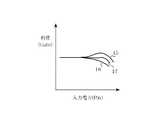
【0019】
図2は、実施の形態1による高周波増幅器の入力電力に対する利得の特性を示す説明図である。図において、15はアンプ1の入力電力(Pin)に対する利得(Gain)の特性曲線、16はアンプ2の入力電力に対する利得の特性曲線、17はアンプ1とアンプ2とを並列合成したアンプAの入力電力に対する利得の特性曲線である。
【0020】
次に動作について説明する。
アンプ1はバイポーラトランジスタ7のベースに容量性素子9を装荷しており、アンプ2はバイポーラトランジスタ8のベースに容量性素子10を装荷していることから、アンプ1とアンプ2とは互いに異なるバイアス条件に設定することが可能で、アンプ1は定電圧駆動によって増幅動作を行い、アンプ2は定電流駆動によって増幅動作を行う。
【0021】
アンプ1の基本的な増幅動作を説明する。RF入力端子3から入力された信号は容量性素子9を介してバイポーラトランジスタ7のベースに入力される。このときバイポーラトランジスタ7のベースには、定電圧ベースバイアス回路12によって一定のベースバイアス電圧が供給されている。また、バイポーラトランジスタ7のコレクタには電源回路14によって電源電力が供給され、増幅された信号は容量性素子11を介してRF出力端子4に出力される。なお、バイポーラトランジスタ7のエミッタは接地されている。
【0022】
アンプ2の基本的な増幅動作を説明する。RF入力端子3から入力された信号は容量性素子10を介してバイポーラトランジスタ8のベースに入力される。このとき、バイポーラトランジスタ8のベースには、定電流ベースバイアス回路13によって一定のベースバイアス電流が供給されている。また、バイポーラトランジスタ8のコレクタには電源回路14によって電源電力が供給され、増幅された信号は容量性素子11を介してRF出力端子4に出力される。なお、バイポーラトランジスタ8のエミッタは接地されている。
【0023】
アンプ1において、バイポーラトランジスタ7のベースに、一定のバイアス電圧を供給し、また、アイドル電流値(DC電圧のみを入力した際にコレクタ・ベース間に流れる電流値)を適切に設定すると、アンプ1の利得特性は図2に示す特性曲線15のようになり、入力信号の大きさが小さい範囲、即ち入力電力が低い範囲では利得が一定で、それ以上入力電力が大きくなると一定の範囲内において、入力電力と共に利得が増加し、さらに入力電力が大きくなると利得が減少する。
【0024】
アンプ2において、入力電力を増幅するバイポーラトランジスタ8のベースに、一定のバイアス電流を供給し、また、アイドル電流値を適切に設定すると、アンプ2の利得特性は図2に示す特性曲線16のようになり、入力電力が低い範囲では利得が一定で、それ以上入力電力が大きくなると利得は減少する。
【0025】
図1に示す定電圧ベースバイアス回路12を用いたアンプ1と、定電流ベースバイアス回路13を用いたアンプ2とを並列合成したアンプAの利得は、図2に示す特性曲線17のようになる。特性曲線17は、特性曲線15や特性曲線16に比べて入力電力の高い範囲まで利得が一定で、出力信号に生じる歪が少ないことを示している。アンプAのように、バイポーラトランジスタ7のベースに定電圧を供給して駆動するアンプ1とバイポーラトランジスタ8のベースに定電流を供給して駆動するアンプ2とを並列合成すると、出力歪が少なくなり広範囲の入力電力について一定の利得が得られ、歪特性の優れた高周波増幅器を成すことができる。
【0026】
アンプ1とアンプ2を並列合成したアンプAは、図2に示す特性曲線17のような入力電力・利得特性を得るため、アンプ1の入力電力・利得特性と、アンプ2の入力電力・利得特性とを調整する。これは、アンプ1の飽和出力電力とアンプ2の飽和出力電力の整合性や、アンプ1の歪特性とアンプ2の歪特性の整合性を考慮したもので、具体的には各々のアンプの増幅素子のトランジスタサイズを調整し、トランジスタサイズ比の最適化および各アンプのアイドル電流値の最適化を行って、アンプ1とアンプ2の整合性を最適化する。
【0027】
図3は、実施の形態1による高周波増幅器の出力電力(Pout)の歪特性を示す説明図である。図において、18はアンプ1の出力電力(Pout)の歪特性曲線、19はアンプ1とアンプ2を並列合成したアンプAの出力電力の歪特性曲線である。
【0028】
通信システムの規格には歪特性の要求値が規定されており、例えば、W−CDMAの規格では、出力電力(Pout)=26.5dBmのとき、隣接チャネル漏洩電力(ACPR)≦−38dBcとなるように定められている。定電圧駆動のアンプ1は、図3の歪特性曲線18に示すように、低い出力電力から歪特性が良好で、出力電力が26.5dBmにおいて隣接チャネル漏洩電力が−38dBcとなる歪特性が得られる。また、低い出力電力範囲では隣接チャネル漏洩電力が−50dBc以下となり、−38dBc以下を要求する規格を満足するものである。このような歪特性を有するアンプ1と定電流駆動のアンプ2を並列合成したアンプAの歪特性は、歪特性曲線19に示すようになる。
【0029】
歪特性曲線19のような歪特性は、アンプ1のアイドル電流値とアンプ2のアイドル電流値の調整・設定によって得られる。具体的には、アンプ1が備えるバイポーラトランジスタ7のエミッタ面積AE1が、アンプ2が備えるバイポーラトランジスタ8のエミッタ面積AE2より大きくなるように(AE1>AE2)各トランジスタサイズを設定し、また、バイポーラトランジスタ7のベースバイアス電圧Vbe1がバイポーラトランジスタ8のベースバイアス電圧Vbe2より大きくなるように(Vbe1>Vbe2)当該回路を構成する。こうすると、低出力電力において隣接チャネル漏洩電力が約−40dBcとなり、また、出力電力が26.5dBmにおいて隣接チャネル漏洩電力が−38dBcとなる良好な歪特性が得られる。
【0030】
また、定電流駆動のアンプ2のアイドル電流値を低く設定し、これに合わせて定電圧駆動のアンプ1のアイドル電流値を調整した場合にも、アンプ1とアンプ2を並列合成したアンプAの歪特性は前記説明のように良好なものとなる。アイドル電流値を低く設定して定電流駆動のアンプ2と定電圧駆動のアンプ1を並列合成すると、優れた歪特性を有しながら後述するように付加効率も良好な高周波増幅器が得られる。
【0031】
次に、実施の形態1の高周波増幅器の付加効率について説明する。
図4は、実施の形態1による高周波増幅器の出力電力(Pout)の付加効率を示す説明図である。図において、20はアンプ1の出力の付加効率を示す特性曲線、21はアンプAの出力の付加効率を示す特性曲線である。
【0032】
アンプAを構成する定電流駆動のアンプ2のアイドル電流値を低く設定し、これに合わせて定電圧駆動のアンプ1のアイドル電流値を調整して最適化すると、図4の特性曲線21に示すような付加効率が得られる。図4の特性曲線21と特性曲線20を比較すると、どのような出力電力においても、アンプ1に比べてアンプAの付加特性が良好で、特に出力電力の低い範囲と飽和出力電力においてアンプAの付加効率がアンプ1に比べて良好であることがわかる。このように、定電流駆動のアンプ2のアイドル電流値を低く設定して、これに合わせて定電圧駆動のアンプ1のアイドル電流値を設定して並列合成すると、障害となるほど歪特性を劣化させることなく付加効率を良好にすることができる。
【0033】
以上のように、この実施の形態1によれば、定電圧駆動のアンプ1と定電流駆動のアンプ2とを並列合成したので、入力電力が高い範囲まで利得を一定に保つことができ、優れた歪特性が得られるという効果がある。
【0034】
また、定電流駆動のアンプ2のアイドル電流値を低く設定して、これに対応させて定電圧駆動のアンプ1のアイドル電流値を調整したので、良好な歪特性が得られ、特に低出力電力や飽和出力電力において優れた付加効率が得られるという効果がある。
【0035】
実施の形態2.
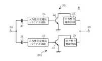
図5は、この発明の実施の形態2による高周波増幅器を示す回路図である。図において、22はベースに供給される定電圧によって駆動される増幅素子のバイポーラトランジスタ、23はベースに供給される定電流によって駆動される増幅素子のバイポーラトランジスタ、24はRF入力端子、25は入力整合回路と定電圧ベースバイアス回路とを一体化した入力整合定電圧バイアス回路、26は出力整合回路と電源回路とを一体化した出力整合電源回路、27は入力整合回路と定電流ベースバイアス回路とを一体化した入力整合定電流バイアス回路、28は出力整合回路と電源回路とを一体化した出力整合電源回路、29はRF出力端子、30はバイポーラトランジスタ22のベースに装荷された容量性素子、31はバイポーラトランジスタ23のベースに装荷された容量性素子、201は増幅素子のバイポーラトランジスタ22と容量性素子30と入力整合定電圧バイアス回路25と出力整合電源回路26とを備えたアンプ(定電圧駆動の増幅手段)、202は増幅素子のバイポーラトランジスタ23と容量性素子31と入力整合定電流バイアス回路27と出力整合電源回路28とを備えたアンプ(定電流駆動の増幅手段)、Bはアンプ201とアンプ202とを並列合成したアンプである。
【0036】
次に動作について説明する。
この実施の形態2による高周波増幅器は、定電圧駆動のアンプ201に入力整合定電圧バイアス回路25と出力整合電源回路26とを備え、また、定電流駆動のアンプ202に入力整合定電流バイアス回路27と出力整合電源回路28とを備えたもので、バイポーラトランジスタ22は図1に示すバイポーラトランジスタ7に相当し、バイポーラトランジスタ23は図1に示すバイポーラトランジスタ8に相当し、また、容量性素子30は図1に示す容量性素子9に、容量性素子31は図1に示す容量性素子10に相当するもので、それぞれ同様な作用効果が得られるものである。
【0037】
実施の形態2によるアンプ201とアンプ202は、それぞれ実施の形態1によるアンプ1とアンプ2に相当する動作を行うもので、増幅素子のバイポーラトランジスタのエミッタ面積やVbe電圧によって設定されるアイドル電流値等は、実施の形態1の説明と同様に取り扱うことができるものである。また、高周波増幅も同様に動作し、出力電力の歪特性や付加効率も同様なものである。このように、実施の形態2によるアンプ201とアンプ202とを並列合成したアンプBは、実施の形態1のアンプ1とアンプ2とを並列合成したアンプAと同様に動作し、作用効果も同様であるため、これらの説明を省略し、実施の形態2のアンプ201とアンプ202の特徴的な動作を説明する。
【0038】
アンプ201は、RF入力端子24から入力された信号を、入力整合定電圧バイアス回路25を用いて整合し、容量性素子30を介してバイポーラトランジスタ22のベースに入力する。このときバイポーラトランジスタ22のベースには、入力整合定電圧バイアス回路25によって一定のベースバイアス電圧が供給されている。また、バイポーラトランジスタ22のコレクタには出力整合電源回路26によって電源電力が供給されている。バイポーラトランジスタ22が増幅した信号は、出力整合電源回路26によって出力整合が行われ、出力整合電源回路28から出力された信号と共にRF出力端子29に出力される。なお、バイポーラトランジスタ22のエミッタは接地されている。
【0039】
アンプ202は、入力整合定電流バイアス回路27を用いてRF入力端子24から入力された信号の入力整合を行い、容量性素子31を介してバイポーラトランジスタ23のベースに入力する。このときバイポーラトランジスタ23のベースには、入力整合定電流バイアス回路27によって一定のベースバイアス電流が供給されている。また、バイポーラトランジスタ23のコレクタには出力整合電源回路28によって電源電力が供給されている。バイポーラトランジスタ23が増幅した信号は、出力整合電源回路28によって出力整合が行われ、出力整合電源回路26から出力された出力電力と共にRF出力端子29に出力される。なお、バイポーラトランジスタ23のエミッタは接地されている。
【0040】
以上のように、この実施の形態2によれば、アンプ201に入力整合回路と定電圧ベースバイアス回路を一体化した入力整合定電圧バイアス回路25と出力整合回路と電源回路とを一体化した出力整合電源回路26とを備え、アンプ202に入力整合回路と定電流ベースバイアス回路を一体化した入力整合定電流バイアス回路27と出力整合回路と電源回路とを一体化した出力整合電源回路28とを備えたので、高周波増幅器を構成する部品点数を削減することができ、また当該高周波増幅器の小型化を図ることができるという効果がある。
【0041】
また、定電圧駆動のアンプ201と定電流駆動のアンプ202を並列合成したので、入力電力が高い範囲まで利得を一定に保つことができ、優れた歪特性が得られるという効果がある。
【0042】
また、定電流駆動のアンプ202のアイドル電流値を低く設定して、これに対応させて定電圧駆動のアンプ201のアイドル電流値を調整したので、良好な歪特性が得られ、特に低出力電力や飽和出力電力において優れた付加効率が得られるという効果がある。
【0043】
実施の形態3.
図6は、この発明の実施の形態3による高周波増幅器を示す回路図である。図において、32はベースに供給された定電圧によって駆動される増幅素子のバイポーラトランジスタ、33はベースに供給された定電流によって駆動される増幅素子のバイポーラトランジスタ、34はRF入力端子、35は入力整合回路と定電圧ベースバイアス回路とを一体化した入力整合定電圧バイアス回路、36は出力整合回路と電源回路とを一体化した出力整合電源回路、37は入力整合回路と定電流ベースバイアス回路とを一体化した入力整合定電流バイアス回路、38はRF出力端子、39はバイポーラトランジスタ32のベースに装荷された容量性素子、40はバイポーラトランジスタ33のベースに装荷された容量性素子、301はバイポーラトランジスタ32を使用して増幅を行うアンプ(定電圧駆動の増幅手段)、302はバイポーラトランジスタを使用して増幅を行うアンプ(定電流駆動の増幅手段)、Cはアンプ301とアンプ302とを並列合成したアンプである。
【0044】
次に動作について説明する。
この実施の形態3による高周波増幅器は、定電圧駆動のアンプ301に入力整合定電圧バイアス回路35を備え、また、定電流駆動のアンプ302に入力整合定電流バイアス回路37を備え、アンプ301とアンプ302を並列合成したアンプCに、アンプ301とアンプ302の出力を整合し、また電源電力を供給する出力整合電源回路36を備えたものである。アンプ301のバイポーラトランジスタ32は図1に示すバイポーラトランジスタ7に相当し、アンプ302のバイポーラトランジスタ33は図1に示すバイポーラトランジスタ8に相当し、また、容量性素子39は図1に示す容量性素子9に、容量性素子40は図1に示す容量性素子10に相当するもので、それぞれ同様な作用効果が得られるものである。
【0045】
実施の形態3によるアンプ301とアンプ302は、それぞれ実施の形態1によるアンプ1とアンプ2に相当する動作を行うもので、増幅素子のバイポーラトランジスタのエミッタ面積やVbe電圧によって設定されるアイドル電流値等は、実施の形態1の説明と同様に取り扱うことができるものである。また、高周波増幅も同様に動作し、出力電力の歪特性や付加効率も同様なものである。このように、実施の形態3によるアンプ301とアンプ302とを並列合成したアンプCは、実施の形態1のアンプ1とアンプ2とを並列合成したアンプAと同様に動作し、作用効果も同様であるため、これらの説明を省略し、実施の形態3のアンプ301とアンプ302の特徴的な動作を説明する。
【0046】
アンプ301は、RF入力端子34から入力された信号を入力整合定電圧バイアス回路35を用いて整合し、容量性素子39を介してバイポーラトランジスタ32のベースに入力する。このときバイポーラトランジスタ32のベースには、入力整合定電圧バイアス回路35によって一定のベースバイアス電圧が供給されている。また、バイポーラトランジスタ32のコレクタには、出力整合電源回路36によって電源電力が供給されている。バイポーラトランジスタ32が増幅した信号は、出力整合電源回路36によってバイポーラトランジスタ33の出力信号と共に整合されてRF出力端子38へ出力される。なお、バイポーラトランジスタ32のエミッタは接地されている。
【0047】
アンプ302は、RF入力端子34から入力された信号を入力整合定電流バイアス回路37を用いて整合し、容量性素子40を介してバイポーラトランジスタ33のベースに入力する。このときバイポーラトランジスタ33のベースには、入力整合定電流バイアス回路35によって一定のベースバイアス電流が供給されている。また、バイポーラトランジスタ33のコレクタには、出力整合電源回路36によって電源電力が供給され、バイポーラトランジスタ33が増幅した信号は、出力整合電源回路36によってバイポーラトランジスタ32の出力信号と共に整合されてRF出力端子38へ出力される。なお、バイポーラトランジスタ33のエミッタは接地されている。
【0048】
以上のように、この実施の形態3によれば、定電圧駆動のアンプ301に入力整合回路と定電圧ベースバイアス回路とを一体化した入力整合定電圧バイアス回路35を備え、定電流駆動のアンプ302に入力整合回路と定電流ベースバイアス回路とを一体化した入力整合定電流バイアス回路37を備え、また、アンプ301とアンプ302の出力電力を整合する出力整合回路とアンプ301とアンプ302に電源電力を供給する電源回路とを一体化した出力整合電源回路36を備えたので、高周波増幅器の部品点数を削減することができ、また当該高周波増幅器の小型化を図ることができるという効果がある。
【0049】
また、定電圧駆動のアンプ301と定電流駆動のアンプ302とを並列合成したので、入力電力が高い範囲まで利得を一定に保つことができ、優れた歪特性を得ることができるという効果がある。
【0050】
また、定電流駆動のアンプ302のアイドル電流値を低く設定して、これに対応させて定電圧駆動のアンプ301のアイドル電流値を調整したので、良好な歪特性が得られ、特に低出力電力や飽和出力電力において優れた付加効率が得られるという効果がある。
【0051】
実施の形態4.
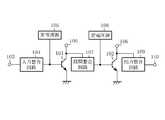
図7は、この発明の実施の形態4による高周波増幅器を示す回路図である。図において、41はベースに供給される定電圧によって駆動される増幅素子のバイポーラトランジスタ、42はベースに供給される定電流によって駆動される増幅素子のバイポーラトランジスタ、43はRF入力端子、44は定電圧ベースバイアス回路(定電圧バイアス回路)、45は出力整合回路と電源回路を一体化した出力整合電源回路、46は定電流ベースバイアス回路(定電流バイアス回路)、47はRF出力端子、48は入力整合回路、49はバイポーラトランジスタ41のベースに装荷された容量性素子、50はバイポーラトランジスタ42のベースに装荷された容量性素子、401はバイポーラトランジスタ41を使用して増幅を行うアンプ(定電圧駆動の増幅手段)、402はバイポーラトランジスタ42を使用して増幅を行うアンプ(定電流駆動の増幅手段)、Dはアンプ401とアンプ402とを並列合成したアンプである。
【0052】
次に動作について説明する。
この実施の形態4による高周波増幅器は、定電圧駆動のアンプ401に定電圧ベースバイアス回路44を備え、また、定電流駆動のアンプ402に定電流ベースバイアス回路46を備え、アンプ401とアンプ402を並列合成したアンプDに、アンプ401とアンプ402に入力する信号の整合を行う入力整合回路48と、アンプ401とアンプ402に電源電力を供給し、またアンプ401とアンプ402の出力信号の整合を行い、RF出力端子47へ出力する出力整合電源回路45を備えたものである。アンプ401のバイポーラトランジスタ41は図1に示すバイポーラトランジスタ7に相当し、アンプ402のバイポーラトランジスタ42は図1に示すバイポーラトランジスタ8に相当し、また、容量性素子49は図1に示す容量性素子9に、容量性素子50は図1に示す容量性素子10に相当するもので、それぞれ同様な作用効果が得られるものである。
【0053】
実施の形態4によるアンプ401とアンプ402は、それぞれ実施の形態1によるアンプ1とアンプ2に相当する動作を行うもので、増幅素子のバイポーラトランジスタのエミッタ面積やVbe電圧によって設定されるアイドル電流値等は、実施の形態1の説明と同様に取り扱うことができるものである。また、高周波増幅も同様に動作し、出力電力の歪特性や付加効率も同様なものである。このように、実施の形態4によるアンプ401とアンプ402とを並列合成したアンプDは、実施の形態1のアンプ1とアンプ2とを並列合成したアンプAと同様に動作し、作用効果も同様であるため、これらの説明を省略し、実施の形態4のアンプ401とアンプ402の特徴的な動作を説明する。
【0054】
アンプDを構成するアンプ401は、RF入力端子43から入力され、入力整合回路48によって整合された信号を、定電圧ベースバイアス回路44を用いて一定の電圧にバイアスし、容量性素子49を介してバイポーラトランジスタ41のベースに入力する。このとき、バイポーラトランジスタ41のコレクタには、出力整合電源回路45によって電源電力が供給され、バイポーラトランジスタ41が増幅した信号は、出力整合電源回路45によってバイポーラトランジスタ42の出力信号と共に整合されてRF出力端子47に出力される。なお、バイポーラトランジスタ41のエミッタは接地されている。
【0055】
アンプDを構成するアンプ402は、RF入力端子43から入力され、入力整合回路48によって整合された信号を、定電流ベースバイアス回路46を用いて一定の電流にバイアスし、容量性素子50を介してバイポーラトランジスタ42のベースに入力する。このとき、バイポーラトランジスタ42のコレクタには、出力整合電源回路45によって電源電力が供給され、バイポーラトランジスタ42が増幅した信号は、出力整合電源回路45によってバイポーラトランジスタ41の出力信号と共に整合されてRF出力端子47に出力される。なお、バイポーラトランジスタ42のエミッタは接地されている。
【0056】
以上のように、この実施の形態4によれば、定電圧駆動のアンプ401と定電流駆動のアンプ402とを並列合成したアンプDに、入力信号の整合を行ってアンプ401およびアンプ402に入力する入力整合回路48と、アンプ401およびアンプ402に電源電力を供給し、アンプ401およびアンプ402の出力信号を整合する出力整合電源回路45とを備えたので、高周波増幅器の部品点数を削減することができ、また当該高周波増幅器の小型化を図ることができるという効果がある。
【0057】
また、定電圧駆動のアンプ401と定電流駆動のアンプ402とを並列合成したので、入力電力が高い範囲まで利得を一定に保つことができ、優れた歪特性を得ることができるという効果がある。
【0058】
また、定電流駆動のアンプ402のアイドル電流値を低く設定し、これに対応させて定電圧駆動のアンプ401のアイドル電流値を調整したので、良好な歪特性が得られ、特に低出力電力や飽和出力電力において優れた付加効率が得られるという効果がある。
【0059】
実施の形態5.
図8は、この発明の実施の形態5による高周波増幅器に用いられる並列合成したバイポーラトランジスタの構成を示す説明図である。図示したものは複数のバイポーラトランジスタを同一チップ上に形成したもので、このチップ上に備えられた複数のベースを定電圧駆動するものと定電流駆動するものとに分けて構成したものである。図において、51は定電圧駆動するバイポーラトランジスタのベースパッド、52は定電流駆動するバイポーラトランジスタのベースパッド、53は各バイポーラトランジスタのコレクタを並列合成するコレクタパッド、54aは定電圧駆動するバイポーラトランジスタのベースとベースパッド51とを接続するベース引き出しパターン、54bは定電流駆動するバイポーラトランジスタのベースとベースパッド52とを接続するベース引き出しパターン、55はエミッタ引き出しパターン、56はコレクタ引き出しパターン、57は各バイポーラトランジスタのエミッタを並列合成するエミッタパッドである。
【0060】
図8に示したものは、例えば、定電圧駆動するバイポーラトランジスタと定電流駆動するバイポーラトランジスタとのエミッタ面積比が2:1になるように構成したものである。これらのバイポーラトランジスタは、コレクタ引き出しパターン56を用いて定電圧駆動するバイポーラトランジスタと定電流駆動するバイポーラトランジスタの各コレクタを一つのコレクタパッド53に接続して合成し、また、エミッタ引き出しパターン55を用いて定電圧駆動するバイポーラトランジスタと定電流駆動するバイポーラトランジスタの各エミッタを一つのエミッタパッド57に接続して合成している。また、各バイポーラトランジスタのエミッタは、エミッタパッド57上に形成されたバイアホール(図示を省略したスルーホール)を介してグランド(図示省略)に接地されている。
【0061】
定電圧駆動するバイポーラトランジスタのベースは、当該ベースを構成する部分から引き出されたベース引き出しパターン54aによってベースパッド51に接続される。また、定電流駆動するバイポーラトランジスタのベースは、当該ベースを構成する部分から引き出されたベース引き出しパターン54bによってベースパッド52に接続される。なお、ベース引き出しパターン54a,54bとエミッタ引き出しパターン55とは、できるだけ重ならないように、好ましくは、できるだけ離れるように構成して、良好な高周波特性が得られるようにする。
【0062】
このように構成して、ベースパッド51に一定のバイアス電圧を供給し、また、ベースパッド52に一定のバイアス電流を供給すると、定電圧駆動するバイポーラトランジスタのベースは一定の電圧でバイアスされ、また定電流駆動するバイポーラトランジスタのベースは一定の電流でバイアスされる。
【0063】
なお、実施の形態2の高周波増幅器のように、定電圧駆動のアンプと定電流駆動のアンプに個別の電源回路を用いて電源電力を供給する構成の場合には、各バイポーラトランジスタのコレクタを個別に備えたコレクタパッドに接続して構成する。
また、この実施の形態5で説明したように定電圧で駆動するバイポーラトランジスタと定電流で駆動するバイポーラトランジスタとを並列合成して、実施の形態1〜4で説明した高周波増幅器に用いることも可能である。
【0064】
以上のように、この実施の形態5によれば、複数のバイポーラトランジスタを同一チップ上に形成して、定電圧を供給するベースと定電流を供給するベースとに分けて構成し、複数のコレクタをコレクタ引き出しパターン56を用いて一つのコレクタパッド53に接続し、複数のエミッタをエミッタ引き出しパターン55を用いて一つのエミッタパッド57に接続し、ベース引き出しパターン54aを用いて定電圧駆動するバイポーラトランジスタのベースと定電圧が供給されるベースパッド51とを接続し、ベース引き出しパターン54bを用いて定電流駆動するバイポーラトランジスタと定電流が供給されるベースパッド52とを接続するようにしたので、小型化を図りながら複数のバイポーラトランジスタを並列合成して同一チップ上に形成することができるという効果がある。
【0065】
実施の形態6.
次に、この発明の実施の形態6による高周波増幅器を説明する。実施の形態6による高周波増幅器は、実施の形態1〜4で説明した高周波増幅器の定電圧駆動のアンプに用いる増幅素子に、バイポーラトランジスタに代えてFETを使用して構成したものである。FETのゲートに一定のバイアス電圧を供給することで、バイポーラトランジスタを使用したものと同様に増幅動作を行い、また同様な作用効果が得られる。
【0066】
なお、実施の形態1〜4ではバイポーラトランジスタを増幅素子に使用した高周波増幅器を説明したが、SiBJT、SiGeBJT、In Gap等の化合物から成るHBTを増幅素子として使用しても同様な作用効果が得られる。
【0067】
また、前記各実施の形態では、定電圧ベースバイアスによって駆動されるバイポーラトランジスタと、定電流ベースバイアスによって駆動されるバイポーラトランジスタが、それぞれ一つずつ並列合成されたものを例示して説明したが、この発明の高周波増幅器はこれに限定されず、当該高周波増幅器をn個(nは2以上の整数)のアンプ(増幅手段)で構成し、m個(mは1以上n−1以下の整数)の定電流駆動のアンプと、n−m個の定電圧駆動のアンプとを並列合成して実施することができるもので、このように構成したものであれば同様な作用効果が得られる。
【0068】
以上のように、この実施の形態6によれば、定電圧駆動のアンプの増幅素子にFETを用いて構成し、定電圧で駆動するアンプと定電流で駆動するアンプとを並列合成したので、優れた歪特性を有しながら付加効率も良好にできるという効果がある。
【0069】
【発明の効果】
以上のように、この発明によれば、一定の電圧でバイアスする増幅素子を用いた定電圧駆動の増幅手段と、一定の電流でバイアスする増幅素子を用いた定電流駆動の増幅手段とを並列合成したので、優れた歪特性を有しながら良好な付加効率を得ることができるという効果がある。
【0070】
この発明によれば、n個(nは2以上の整数)の増幅手段を備え、当該増幅手段はm個(mは1以上n−1以下の整数)の定電流駆動の増幅手段とn−m個の定電圧駆動の増幅手段とを並列合成したので、優れた歪特性を有しながら良好な付加効率を得ることができるという効果がある。
【0071】
この発明によれば、定電圧駆動の増幅手段が、増幅素子としてバイポーラトランジスタを使用して当該バイポーラトランジスタのベースを一定の電圧でバイアスし、定電流駆動の増幅手段が、増幅素子としてバイポーラトランジスタを使用して当該バイポーラトランジスタのベースを一定の電流でバイアスするようにしたので、優れた歪特性を有しながら良好な付加効率を得ることができるという効果がある。
【0072】
この発明によれば、定電圧駆動の増幅手段が、入力整合を行うと共に一定のバイアス電圧を増幅素子に供給する入力整合定電圧バイアス回路と、出力整合を行うと共に増幅素子に電源電力を供給する出力整合電源回路とを備え、定電流駆動の増幅手段が、入力整合を行うと共に一定のバイアス電流を増幅素子に供給する入力整合定電流バイアス回路と、出力整合を行うと共に増幅素子に電源電力を供給する出力整合電源回路とを備えたので、当該高周波増幅器を構成する部品点数が削減でき、小型化が図れるという効果がある。
【0073】
この発明によれば、定電圧駆動の増幅手段および定電流駆動の増幅手段に電源電力を供給すると共に定電圧駆動の増幅手段および定電流駆動の増幅手段の出力整合を行う出力整合電源回路を備え、定電圧駆動の増幅手段が、入力の整合を行うと共に一定のバイアス電圧を増幅素子に供給する入力整合定電圧バイアス回路を備え、定電流駆動の増幅手段が、入力の整合を行うと共に一定のバイアス電流を増幅素子に供給する入力整合定電流バイアス回路を備えたので、当該高周波増幅器を構成する部品点数が削減でき、小型化が図れるという効果がある。
【0074】
この発明によれば、定電圧駆動の増幅手段および定電流駆動の増幅手段の入力整合を行う入力整合回路と、定電圧駆動の増幅手段および定電流駆動の増幅手段に電源電力を供給すると共に定電圧駆動の増幅手段および定電流駆動の増幅手段の出力整合を行う出力整合電源回路とを備え、定電圧駆動の増幅手段が、一定のバイアス電圧を増幅素子に供給する定電圧バイアス回路を備え、定電流駆動の増幅手段が、一定のバイアス電流を増幅素子に供給する定電流バイアス回路を備えたので、当該高周波増幅器を構成する部品点数が削減でき、小型化が図れるという効果がある。
【0075】
この発明によれば、増幅素子が、同一チップ上に一定の電圧でバイアスするバイポーラトランジスタのベースと一定の電流でバイアスするバイポーラトランジスタのベースとを分離して構成し、一定の電圧でバイアスするバイポーラトランジスタのコレクタと一定の電流でバイアスするバイポーラトランジスタのコレクタとを一つのコレクタパッドに接続するコレクタ引き出しパターンと、一定の電圧でバイアスするバイポーラトランジスタのエミッタと一定の電流でバイアスするバイポーラトランジスタのエミッタとを一つのエミッタパッドに接続するエミッタ引き出しパターンと、一定の電圧でバイアスするバイポーラトランジスタのベースと一定のバイアス電圧が供給されるベースパッドとを接続するベース引き出しパターンと、一定の電流でバイアスするバイポーラトランジスタのベースと一定のバイアス電流が供給されるベースパッドとを接続するベース引き出しパターンとを備え、ベース引き出しパターンとエミッタ引き出しパターンとが重なる部分を少なく構成したので、良好な高周波特性を確保して小型化を図りながら複数のバイポーラトランジスタを並列合成して同一チップ上に形成することができるという効果がある。
【0076】
この発明によれば、定電圧駆動の増幅手段が、増幅素子としてFETを使用して当該FETのゲートを一定の電圧でバイアスし、定電流駆動の増幅手段が、増幅素子としてバイポーラトランジスタを使用して当該バイポーラトランジスタのベースを一定の電流でバイアスするようにしたので、優れた歪特性を有しながら良好な付加効率を得ることができるという効果がある。
【図面の簡単な説明】
【図1】 この発明の実施の形態1による高周波増幅器を示す回路図である
【図2】 実施の形態1による高周波増幅器の入力電力に対する利得の特性を示す説明図である。
【図3】 実施の形態1による高周波増幅器の出力電力の歪特性を示す説明図である。
【図4】 実施の形態1による高周波増幅器の出力電力の付加効率を示す説明図である。
【図5】 この発明の実施の形態2による高周波増幅器を示す回路図である。
【図6】 この発明の実施の形態3による高周波増幅器を示す回路図である。
【図7】 この発明の実施の形態4による高周波増幅器を示す回路図である。
【図8】 この発明の実施の形態5による高周波増幅器に用いられる並列合成したバイポーラトランジスタの構成を示す説明図である。
【図9】 従来の高周波増幅器を示す構成図である。
【符号の説明】
1 アンプ(定電圧駆動の増幅手段)、2 アンプ(定電流駆動の増幅手段)、3 RF入力端子、4 RF出力端子、5,6 特性曲線、7,8 バイポーラトランジスタ、9,10,11 容量性素子、12 定電圧ベースバイアス回路(定電圧バイアス回路)、13 定電流ベースバイアス回路(定電流バイアス回路)、14 電源回路、15,16,17 特性曲線、18,19 歪特性曲線、20,21 特性曲線、22,23 バイポーラトランジスタ、24 RF入力端子、25 入力整合定電圧バイアス回路、26 出力整合電源回路、27入力整合定電流バイアス回路、28 出力整合電源回路、29 RF出力端子、30,31 容量性素子、32,33 バイポーラトランジスタ、34 RF入力端子、35 入力整合定電圧バイアス回路、36 出力整合電源回路、37入力整合定電流バイアス回路、38 RF出力端子、39,40 容量性素子、41,42 バイポーラトランジスタ、43 RF入力端子、44 定電圧ベースバイアス回路(定電圧バイアス回路)、45 出力整合電源回路、46 定電流ベースバイアス回路(定電流バイアス回路)、47 RF出力端子、48 入力整合回路、49,50 容量性素子、51,52 ベースパッド、53 コレクタパッド、54a,54b ベース引き出しパターン、55 エミッタ引き出しパターン、56 コレクタ引き出しパターン、57 エミッタパッド、201 アンプ(定電圧駆動の増幅手段)、202 アンプ(定電流駆動の増幅手段)、301 アンプ(定電圧駆動の増幅手段)、302 アンプ(定電流駆動の増幅手段)、401 アンプ(定電圧駆動の増幅手段)、402 アンプ(定電流駆動の増幅手段)、A,B,C,D アンプ。[0001]
BACKGROUND OF THE INVENTION
The present invention relates to a high frequency amplifier using a bipolar transistor.
[0002]
[Prior art]
A high frequency amplifier used for a digital cellular phone or the like is required to have low distortion characteristics in order to prevent interference with an adjacent channel. Therefore, the high-frequency amplifier improves the distortion characteristics by compressing the gain of the transistor used for amplification and suppressing the phase rotation.
[0003]
In the conventional high frequency amplifier, a diode, FET, bipolar transistor or the like is connected to the transistor of the amplifying element to suppress phase rotation in the entire amplifying circuit, and the gain is compressed to compensate for low distortion characteristics.
FIG. 9 is a block diagram showing a conventional high-frequency amplifier. This figure shows a two-stage high-frequency amplifier disclosed in Japanese Patent Laid-Open No. 10-135750 as an example of a conventional high-frequency amplifier. In the figure, 101 is a bipolar transistor in the previous stage, 102 is a bipolar transistor in the subsequent stage, 103 is an RF input terminal, 104 is an input matching circuit of the
[0004]
Next, the operation will be described.
The amplifier circuit in the previous stage is operated while holding the base current of the
[0005]
As described above, when the
[0006]
[Problems to be solved by the invention]
Since the conventional high-frequency amplifier is configured as described above, it combines at least two stages of a bipolar transistor amplifier circuit that keeps the base current constant and a bipolar transistor amplifier circuit that keeps the base voltage constant. There has been a problem that the size of the high-frequency amplifier is increased. In order to improve the distortion characteristics, it is necessary to increase the emitter size of the post-stage transistor and to set the idle current value (current value flowing between the collector and base when a DC voltage is applied) to a large value. Then, there is a problem that the additional efficiency is deteriorated particularly at a low output, and the additional efficiency is lowered even at a high output.
[0007]
The present invention has been made to solve the above-described problems. A high-frequency amplifier having high output and excellent distortion characteristics, high added efficiency, and improved added efficiency especially at low output power. The purpose is to obtain.
[0008]
It is another object of the present invention to obtain a high-frequency amplifier having improved distortion characteristics and added efficiency while reducing the size.
[0009]
[Means for Solving the Problems]
The high-frequency amplifier according to the present invention is a parallel synthesis of a constant voltage drive amplification means using an amplification element biased with a constant voltage and a constant current drive amplification means using an amplification element biased with a constant current. It is.
[0010]
The high-frequency amplifier according to the present invention includes n (n is an integer of 2 or more) amplification means, and the amplification means includes m (m is an integer of 1 to n-1) constant current drive amplification means. This is a parallel synthesis of nm constant voltage drive amplifying means.
[0011]
In the high-frequency amplifier according to the present invention, the constant voltage drive amplifying means uses a bipolar transistor as an amplifying element to bias the base of the bipolar transistor at a constant voltage, and the constant current drive amplifying means is bipolar as the amplifying element. A transistor is used to bias the base of the bipolar transistor with a constant current.
[0012]
The high frequency amplifier according to the present invention includes an input matching constant voltage bias circuit in which a constant voltage drive amplification means performs input matching and supplies a constant bias voltage to the amplification element, and performs output matching and supplies power to the amplification element. And an output matching power supply circuit for supplying, an input matching constant current bias circuit for supplying a constant bias current to the amplifying element, and a constant current driving amplifying means for performing input matching and supplying power to the amplifying element And an output matching power supply circuit for supplying power.
[0013]
The high frequency amplifier according to the present invention provides an output matching power supply circuit for supplying power to the constant voltage drive amplification means and the constant current drive amplification means and performing output matching between the constant voltage drive amplification means and the constant current drive amplification means The constant voltage drive amplifying means performs input matching and an input matching constant voltage bias circuit for supplying a constant bias voltage to the amplifying element, and the constant current drive amplifying means performs input matching. An input matching constant current bias circuit for supplying a constant bias current to the amplifying element is provided.
[0014]
The high-frequency amplifier according to the present invention supplies power to the input matching circuit for performing input matching between the constant voltage drive amplification means and the constant current drive amplification means, and the constant voltage drive amplification means and the constant current drive amplification means. And an output matching power supply circuit that performs output matching of the constant voltage drive amplification means and the constant current drive amplification means, and the constant voltage drive amplification means includes a constant voltage bias circuit that supplies a constant bias voltage to the amplification element. The constant current drive amplifying means includes a constant current bias circuit for supplying a constant bias current to the amplifying element.
[0015]
In the high-frequency amplifier according to the present invention, the amplifying element is configured such that the base of the bipolar transistor biased with a constant voltage and the base of the bipolar transistor biased with a constant current are separated on the same chip and biased with a constant voltage. A collector lead pattern for connecting a collector of a bipolar transistor and a collector of a bipolar transistor biased at a constant current to one collector pad, an emitter of a bipolar transistor biased at a constant voltage, and a bipolar transistor biased at a constant current A base lead pattern for connecting an emitter lead pattern for connecting an emitter to one emitter pad, a base of a bipolar transistor biased at a constant voltage, and a base pad to which a constant bias voltage is supplied And a base lead pattern that connects a base of a bipolar transistor that is biased with a constant current and a base pad that is supplied with a constant bias current, and the portion where the base lead pattern and the emitter lead pattern overlap is reduced. Is.
[0016]
In the high frequency amplifier according to the present invention, the constant voltage drive amplifying means uses a FET as an amplifying element and biases the gate of the FET at a constant voltage, and the constant current driven amplifying means uses a bipolar transistor as the amplifying element. It is used to bias the base of the bipolar transistor with a constant current.
[0017]
DETAILED DESCRIPTION OF THE INVENTION
An embodiment of the present invention will be described below.
Embodiment 1 FIG.
1 is a circuit diagram showing a high-frequency amplifier according to Embodiment 1 of the present invention. In the figure, reference numeral 1 denotes an amplifier (constant voltage driving amplifying means) which is constituted by a bipolar transistor 7 of an amplifying element and a bias circuit and is driven by supplying a constant voltage to the base of the bipolar transistor 7.
[0018]
7 is a bipolar transistor of the amplifying element constituting the amplifier 1, 8 is a bipolar transistor of the amplifying element constituting the
At least the bipolar transistor 7 and the bipolar transistor 8 are formed on the same chip.
FIG. 1B shows an example of a specific circuit configuration of the high-frequency amplifier shown in FIG.
[0019]
FIG. 2 is an explanatory diagram illustrating a gain characteristic with respect to input power of the high-frequency amplifier according to the first embodiment. In the figure, 15 is a gain (Gain) characteristic curve with respect to the input power (Pin) of the
[0020]
Next, the operation will be described.
Since the amplifier 1 is loaded with the capacitive element 9 at the base of the bipolar transistor 7 and the
[0021]
A basic amplification operation of the amplifier 1 will be described. A signal input from the
[0022]
A basic amplification operation of the
[0023]
When a constant bias voltage is supplied to the base of the bipolar transistor 7 in the amplifier 1 and an idle current value (current value flowing between the collector and the base when only a DC voltage is input) is appropriately set, the amplifier 1 2 has a
[0024]
In the
[0025]
The gain of the amplifier A in which the amplifier 1 using the constant voltage
[0026]
The amplifier A in which the amplifier 1 and the
[0027]
FIG. 3 is an explanatory diagram showing distortion characteristics of the output power (Pout) of the high-frequency amplifier according to the first embodiment. In the figure, 18 is a distortion characteristic curve of the output power (Pout) of the
[0028]
The required value of distortion characteristics is defined in the communication system standard. For example, in the W-CDMA standard, when the output power (Pout) = 26.5 dBm, the adjacent channel leakage power (ACPR) ≦ −38 dBc. It is prescribed as follows. As shown by the distortion
[0029]
A distortion characteristic such as the distortion
[0030]
In addition, when the idle current value of the constant
[0031]
Next, the additional efficiency of the high frequency amplifier according to the first embodiment will be described.
FIG. 4 is an explanatory diagram showing the added efficiency of the output power (Pout) of the high-frequency amplifier according to the first embodiment. In the figure, 20 is a characteristic curve showing the added efficiency of the output of the
[0032]
When the idle current value of the constant
[0033]
As described above, according to the first embodiment, since the constant voltage drive amplifier 1 and the constant
[0034]
In addition, since the idle current value of the constant
[0035]
FIG. 5 is a circuit diagram showing a high frequency amplifier according to
[0036]
Next, the operation will be described.
The high-frequency amplifier according to the second embodiment includes an input matching constant
[0037]
The
[0038]
The
[0039]
The
[0040]
As described above, according to the second embodiment, the input matching constant
[0041]
In addition, since the constant
[0042]
Further, since the idle current value of the constant
[0043]
FIG. 6 is a circuit diagram showing a high frequency amplifier according to
[0044]
Next, the operation will be described.
The high-frequency amplifier according to the third embodiment includes an input matching constant
[0045]
The
[0046]
The
[0047]
The
[0048]
As described above, according to the third embodiment, the constant
[0049]
Further, since the constant
[0050]
In addition, since the idle current value of the constant
[0051]
Embodiment 4 FIG.
FIG. 7 is a circuit diagram showing a high frequency amplifier according to Embodiment 4 of the present invention. In the figure, 41 is an amplifying element bipolar transistor driven by a constant voltage supplied to the base, 42 is an amplifying element bipolar transistor driven by a constant current supplied to the base, 43 is an RF input terminal, and 44 is a constant voltage. Voltage base bias circuit (constant voltage bias circuit), 45 is an output matching power supply circuit in which an output matching circuit and a power supply circuit are integrated, 46 is a constant current base bias circuit (constant current bias circuit), 47 is an RF output terminal, and 48 is An input matching circuit, 49 is a capacitive element loaded on the base of the
[0052]
Next, the operation will be described.
In the high-frequency amplifier according to the fourth embodiment, the constant
[0053]
The
[0054]
The
[0055]
The
[0056]
As described above, according to the fourth embodiment, the input signal is matched to the amplifier D in which the constant
[0057]
Further, since the constant
[0058]
In addition, since the idle current value of the constant
[0059]
Embodiment 5. FIG.
FIG. 8 is an explanatory view showing the configuration of a parallel synthesized bipolar transistor used in the high-frequency amplifier according to Embodiment 5 of the present invention. In the figure, a plurality of bipolar transistors are formed on the same chip, and a plurality of bases provided on the chip are divided into those for constant voltage driving and those for constant current driving. In the figure, 51 is a base pad of a bipolar transistor that is driven at a constant voltage, 52 is a base pad of a bipolar transistor that is driven at a constant current, 53 is a collector pad that combines the collectors of the bipolar transistors in parallel, and 54a is a bipolar transistor that is driven at a constant voltage. A base lead pattern for connecting the base and the
[0060]
For example, the configuration shown in FIG. 8 is configured such that the emitter area ratio of a bipolar transistor driven at a constant voltage and a bipolar transistor driven at a constant current is 2: 1. These bipolar transistors are synthesized by connecting the collectors of a bipolar transistor driven at a constant voltage and a collector of a bipolar transistor driven at a constant current using a collector lead-
[0061]
The base of the bipolar transistor driven at a constant voltage is connected to the
[0062]
With this configuration, when a constant bias voltage is supplied to the
[0063]
In the case of a configuration in which power supply power is supplied to each of the constant voltage drive amplifier and the constant current drive amplifier using separate power supply circuits as in the high frequency amplifier of the second embodiment, the collector of each bipolar transistor is individually connected. Connected to the collector pad prepared for
Further, as described in the fifth embodiment, a bipolar transistor driven by a constant voltage and a bipolar transistor driven by a constant current can be combined in parallel and used for the high-frequency amplifier described in the first to fourth embodiments. It is.
[0064]
As described above, according to the fifth embodiment, a plurality of bipolar transistors are formed on the same chip and divided into a base for supplying a constant voltage and a base for supplying a constant current, and a plurality of collectors are provided. Is connected to one
[0065]
Embodiment 6 FIG.
Next, a high frequency amplifier according to Embodiment 6 of the present invention will be described. The high-frequency amplifier according to the sixth embodiment is configured by using an FET instead of a bipolar transistor as an amplifying element used for the constant voltage drive amplifier of the high-frequency amplifier described in the first to fourth embodiments. By supplying a constant bias voltage to the gate of the FET, an amplification operation is performed in the same manner as that using a bipolar transistor, and the same effect can be obtained.
[0066]
In the first to fourth embodiments, the high-frequency amplifier using a bipolar transistor as an amplifying element has been described. However, similar effects can be obtained even when an HBT made of a compound such as SiBJT, SiGeBJT, or In Gap is used as an amplifying element. It is done.
[0067]
In each of the above-described embodiments, the bipolar transistor driven by the constant voltage base bias and the bipolar transistor driven by the constant current base bias are illustrated and described in parallel as one example. The high-frequency amplifier of the present invention is not limited to this, and the high-frequency amplifier is composed of n (n is an integer of 2 or more) amplifiers (amplifying means), and m (m is an integer of 1 to n-1). The constant current drive amplifier and the nm constant voltage drive amplifiers can be combined and implemented in parallel, and similar effects can be obtained with such a configuration.
[0068]
As described above, according to the sixth embodiment, the amplifying element of the constant voltage driving amplifier is configured by using the FET, and the amplifier driven by the constant voltage and the amplifier driven by the constant current are combined in parallel. There is an effect that addition efficiency can be improved while having excellent distortion characteristics.
[0069]
【The invention's effect】
As described above, according to the present invention, the constant voltage driving amplifying means using the amplifying element biased with a constant voltage and the constant current driving amplifying means using the amplifying element biased with a constant current are arranged in parallel. Since they are synthesized, there is an effect that good additive efficiency can be obtained while having excellent distortion characteristics.
[0070]
According to the present invention, n (n is an integer of 2 or more) amplifying means are provided, and the amplifying means includes m (m is an integer of 1 to n−1) constant current drive amplifying means and n−. Since m constant voltage drive amplifying means are combined in parallel, there is an effect that good additional efficiency can be obtained while having excellent distortion characteristics.
[0071]
According to this invention, the constant voltage drive amplifying means uses a bipolar transistor as an amplifying element to bias the base of the bipolar transistor at a constant voltage, and the constant current drive amplifying means uses a bipolar transistor as the amplifying element. Since the base of the bipolar transistor is biased with a constant current by using it, there is an effect that good additional efficiency can be obtained while having excellent distortion characteristics.
[0072]
According to the present invention, the constant voltage drive amplifying means performs input matching and an input matching constant voltage bias circuit that supplies a constant bias voltage to the amplifying element, and performs output matching and supplies power to the amplifying element. An output matching power supply circuit, and a constant current drive amplifying means performs input matching and supplies a constant bias current to the amplifying element, and performs output matching and supplies power to the amplifying element. Since the output matching power supply circuit to be supplied is provided, the number of parts constituting the high-frequency amplifier can be reduced and the size can be reduced.
[0073]
According to the present invention, there is provided an output matching power supply circuit for supplying power to the constant voltage drive amplifying means and the constant current drive amplifying means and performing output matching of the constant voltage drive amplifying means and the constant current drive amplifying means. The constant voltage drive amplifying means includes an input matching constant voltage bias circuit that performs input matching and supplies a constant bias voltage to the amplifying element, and the constant current drive amplifying means performs input matching and is constant. Since the input matching constant current bias circuit for supplying the bias current to the amplifying element is provided, the number of components constituting the high-frequency amplifier can be reduced, and the size can be reduced.
[0074]
According to the present invention, the power supply power is supplied to the input matching circuit that performs input matching between the constant voltage drive amplification unit and the constant current drive amplification unit, and the constant voltage drive amplification unit and the constant current drive amplification unit. An output matching power supply circuit that performs output matching of the voltage-driven amplification unit and the constant-current drive amplification unit, and the constant-voltage drive amplification unit includes a constant voltage bias circuit that supplies a constant bias voltage to the amplification element, Since the constant current drive amplifying means includes a constant current bias circuit for supplying a constant bias current to the amplifying element, the number of parts constituting the high frequency amplifier can be reduced, and the size can be reduced.
[0075]
According to the present invention, the amplifying element is configured such that the base of the bipolar transistor biased at a constant voltage and the base of the bipolar transistor biased at a constant current are separated on the same chip, and the bipolar biased at a constant voltage. A collector lead pattern for connecting the collector of the transistor and the collector of the bipolar transistor biased at a constant current to one collector pad, an emitter of the bipolar transistor biased at a constant voltage, and an emitter of the bipolar transistor biased at a constant current An emitter lead pattern for connecting a single emitter pad, a base lead pattern for connecting a base of a bipolar transistor biased at a constant voltage and a base pad supplied with a constant bias voltage, and a constant It has a base lead pattern that connects the base of a bipolar transistor that is biased with a current and a base pad to which a constant bias current is supplied, and has a structure that has few overlapping portions between the base lead pattern and the emitter lead pattern, so that good high frequency There is an effect that a plurality of bipolar transistors can be synthesized in parallel and formed on the same chip while ensuring characteristics and downsizing.
[0076]
According to this invention, the constant voltage drive amplification means uses the FET as an amplification element and biases the gate of the FET at a constant voltage, and the constant current drive amplification means uses a bipolar transistor as the amplification element. Thus, since the base of the bipolar transistor is biased with a constant current, there is an effect that a good additional efficiency can be obtained while having excellent distortion characteristics.
[Brief description of the drawings]
FIG. 1 is a circuit diagram showing a high-frequency amplifier according to a first embodiment of the present invention.
FIG. 2 is an explanatory diagram illustrating a gain characteristic with respect to input power of the high-frequency amplifier according to the first embodiment.
FIG. 3 is an explanatory diagram showing distortion characteristics of output power of the high-frequency amplifier according to the first embodiment.
FIG. 4 is an explanatory diagram showing the added efficiency of output power of the high-frequency amplifier according to the first embodiment.
FIG. 5 is a circuit diagram showing a high frequency amplifier according to a second embodiment of the present invention.
FIG. 6 is a circuit diagram showing a high frequency amplifier according to a third embodiment of the present invention.
FIG. 7 is a circuit diagram showing a high frequency amplifier according to a fourth embodiment of the present invention.
FIG. 8 is an explanatory diagram showing the configuration of a parallel synthesized bipolar transistor used in a high frequency amplifier according to a fifth embodiment of the present invention.
FIG. 9 is a configuration diagram showing a conventional high-frequency amplifier.
[Explanation of symbols]
1 amplifier (amplifier for constant voltage drive), 2 amplifier (amplifier for constant current drive), 3 RF input terminal, 4 RF output terminal, 5, 6 characteristic curve, 7, 8 bipolar transistor, 9, 10, 11 capacity 12 constant voltage base bias circuit (constant voltage bias circuit), 13 constant current base bias circuit (constant current bias circuit), 14 power supply circuit, 15, 16, 17 characteristic curve, 18, 19 distortion characteristic curve, 20, 21 characteristic curve, 22, 23 bipolar transistor, 24 RF input terminal, 25 input matching constant voltage bias circuit, 26 output matching power supply circuit, 27 input matching constant current bias circuit, 28 output matching power supply circuit, 29 RF output terminal, 30, 31 capacitive element, 32, 33 bipolar transistor, 34 RF input terminal, 35 input matching constant voltage bias circuit, 36 output Combined power supply circuit, 37 input matching constant current bias circuit, 38 RF output terminal, 39, 40 capacitive element, 41, 42 bipolar transistor, 43 RF input terminal, 44 constant voltage base bias circuit (constant voltage bias circuit), 45 output Matching power supply circuit, 46 constant current base bias circuit (constant current bias circuit), 47 RF output terminal, 48 input matching circuit, 49, 50 capacitive element, 51, 52 base pad, 53 collector pad, 54a, 54b Base lead pattern , 55 emitter lead pattern, 56 collector lead pattern, 57 emitter pad, 201 amplifier (constant voltage drive amplification means), 202 amplifier (constant current drive amplification means), 301 amplifier (constant voltage drive amplification means), 302 amplifier (Amplification means for constant current drive), 401 amplifier (constant Pressure driving amplifying means dynamic), amplification means 402 amplifier (constant current drive), A, B, C, D amplifier.
Claims (8)
Translated fromJapanese一定の電圧でバイアスする増幅素子を用いた定電圧駆動の増幅手段と、
一定の電流でバイアスする増幅素子を用いた定電流駆動の増幅手段とを並列合成したことを特徴とする高周波増幅器。In the high frequency amplifier for amplifying a high frequency by using a plurality of amplifying means,
Amplifying means driven by a constant voltage using an amplifying element biased at a constant voltage;
A high-frequency amplifier characterized by combining in parallel a constant current drive amplifying means using an amplifying element biased with a constant current.
定電流駆動の増幅手段は、増幅素子としてバイポーラトランジスタを使用して当該バイポーラトランジスタのベースを一定の電流でバイアスすることを特徴とする請求項2記載の高周波増幅器。The constant voltage drive amplifying means uses a bipolar transistor as an amplifying element and biases the base of the bipolar transistor with a constant voltage,
3. The high frequency amplifier according to claim 2, wherein the constant current drive amplifying means uses a bipolar transistor as an amplifying element and biases the base of the bipolar transistor with a constant current.
定電流駆動の増幅手段は、入力整合を行うと共に一定のバイアス電流を増幅素子に供給する入力整合定電流バイアス回路と、出力整合を行うと共に前記増幅素子に電源電力を供給する出力整合電源回路とを備えたことを特徴とする請求項2記載の高周波増幅器。The constant voltage drive amplifying means includes an input matching constant voltage bias circuit that performs input matching and supplies a constant bias voltage to the amplifying element, an output matching power supply circuit that performs output matching and supplies power to the amplifying element, With
The constant current drive amplifier includes an input matching constant current bias circuit that performs input matching and supplies a constant bias current to the amplifying element, and an output matching power supply circuit that performs output matching and supplies power to the amplifying element. The high frequency amplifier according to claim 2, further comprising:
前記定電圧駆動の増幅手段は、入力の整合を行うと共に一定のバイアス電圧を増幅素子に供給する入力整合定電圧バイアス回路を備え、
前記定電流駆動の増幅手段は、入力の整合を行うと共に一定のバイアス電流を増幅素子に供給する入力整合定電流バイアス回路を備えたことを特徴とする請求項2記載の高周波増幅器。An output matching power supply circuit for supplying power to the constant voltage drive amplification means and the constant current drive amplification means and performing output matching of the constant voltage drive amplification means and the constant current drive amplification means;
The constant voltage drive amplifying means includes an input matching constant voltage bias circuit that performs input matching and supplies a constant bias voltage to the amplifying element,
3. The high frequency amplifier according to claim 2, wherein the constant current drive amplifying means includes an input matching constant current bias circuit that performs input matching and supplies a constant bias current to the amplifying element.
前記定電圧駆動の増幅手段および前記定電流駆動の増幅手段に電源電力を供給すると共に前記定電圧駆動の増幅手段および前記定電流駆動の増幅手段の出力整合を行う出力整合電源回路とを備え、
前記定電圧駆動の増幅手段は、一定のバイアス電圧を増幅素子に供給する定電圧バイアス回路を備え、
前記定電流駆動の増幅手段は、一定のバイアス電流を増幅素子に供給する定電流バイアス回路を備えたことを特徴とする請求項2記載の高周波増幅器。An input matching circuit for performing input matching of the constant voltage drive amplification means and the constant current drive amplification means;
An output matching power supply circuit that supplies power to the constant voltage drive amplification means and the constant current drive amplification means and performs output matching of the constant voltage drive amplification means and the constant current drive amplification means,
The constant voltage drive amplifying means includes a constant voltage bias circuit for supplying a constant bias voltage to the amplifying element,
3. The high frequency amplifier according to claim 2, wherein the constant current drive amplifying means includes a constant current bias circuit for supplying a constant bias current to the amplifying element.
前記一定の電圧でバイアスするバイポーラトランジスタのコレクタと前記一定の電流でバイアスするバイポーラトランジスタのコレクタとを一つのコレクタパッドに接続するコレクタ引き出しパターンと、
前記一定の電圧でバイアスするバイポーラトランジスタのエミッタと前記一定の電流でバイアスするバイポーラトランジスタのエミッタとを一つのエミッタパッドに接続するエミッタ引き出しパターンと、
前記一定の電圧でバイアスするバイポーラトランジスタのベースと一定のバイアス電圧が供給されるベースパッドとを接続するベース引き出しパターンと、
前記一定の電流でバイアスするバイポーラトランジスタのベースと一定のバイアス電流が供給されるベースパッドとを接続するベース引き出しパターンとを備え、
前記ベース引き出しパターンと前記エミッタ引き出しパターンとが重なる部分を少なく構成したことを特徴とする請求項1記載の高周波増幅器。The amplifying element is configured by separating a bipolar transistor base biased with a constant voltage and a bipolar transistor base biased with a constant current on the same chip,
A collector lead pattern for connecting a collector of the bipolar transistor biased at the constant voltage and a collector of the bipolar transistor biased at the constant current to one collector pad;
An emitter lead pattern connecting the emitter of the bipolar transistor biased with the constant voltage and the emitter of the bipolar transistor biased with the constant current to one emitter pad;
A base lead pattern connecting a base of the bipolar transistor biased at the constant voltage and a base pad supplied with the constant bias voltage;
A base lead pattern connecting a base of the bipolar transistor biased with the constant current and a base pad supplied with the constant bias current;
2. The high frequency amplifier according to claim 1, wherein a portion where the base lead pattern and the emitter lead pattern overlap is reduced.
定電流駆動の増幅手段は、増幅素子としてバイポーラトランジスタを使用して当該バイポーラトランジスタのベースを一定の電流でバイアスすることを特徴とする請求項2記載の高周波増幅器。The constant voltage drive amplifying means uses a FET as an amplifying element, biases the gate of the FET with a constant voltage,
3. The high frequency amplifier according to claim 2, wherein the constant current drive amplifying means uses a bipolar transistor as an amplifying element and biases the base of the bipolar transistor with a constant current.
Priority Applications (3)
| Application Number | Priority Date | Filing Date | Title |
|---|---|---|---|
| JP2002024268AJP4130317B2 (en) | 2002-01-31 | 2002-01-31 | High frequency amplifier |
| EP03733370AEP1515434A4 (en) | 2002-01-31 | 2003-06-11 | HIGH FREQUENCY AMPLIFIER |
| PCT/JP2003/007426WO2004112244A1 (en) | 2002-01-31 | 2003-06-11 | High-frequency amplifier |
Applications Claiming Priority (2)
| Application Number | Priority Date | Filing Date | Title |
|---|---|---|---|
| JP2002024268AJP4130317B2 (en) | 2002-01-31 | 2002-01-31 | High frequency amplifier |
| PCT/JP2003/007426WO2004112244A1 (en) | 2002-01-31 | 2003-06-11 | High-frequency amplifier |
Publications (3)
| Publication Number | Publication Date |
|---|---|
| JP2003229728A JP2003229728A (en) | 2003-08-15 |
| JP2003229728A5 JP2003229728A5 (en) | 2005-08-11 |
| JP4130317B2true JP4130317B2 (en) | 2008-08-06 |
Family
ID=34219659
Family Applications (1)
| Application Number | Title | Priority Date | Filing Date |
|---|---|---|---|
| JP2002024268AExpired - LifetimeJP4130317B2 (en) | 2002-01-31 | 2002-01-31 | High frequency amplifier |
Country Status (3)
| Country | Link |
|---|---|
| EP (1) | EP1515434A4 (en) |
| JP (1) | JP4130317B2 (en) |
| WO (1) | WO2004112244A1 (en) |
Families Citing this family (11)
| Publication number | Priority date | Publication date | Assignee | Title |
|---|---|---|---|---|
| JP4130317B2 (en)* | 2002-01-31 | 2008-08-06 | 三菱電機株式会社 | High frequency amplifier |
| US7161433B2 (en) | 2003-06-11 | 2007-01-09 | Mitsubishi Denki Kabushiki Kaisha | High-frequency amplifier |
| JP4567577B2 (en) | 2005-11-08 | 2010-10-20 | 三菱電機株式会社 | Power amplifier bias circuit |
| US8368817B2 (en)* | 2006-01-16 | 2013-02-05 | Nxp B.V. | Filter device |
| JP4611934B2 (en)* | 2006-05-26 | 2011-01-12 | 三菱電機株式会社 | Power amplifier bias circuit |
| JP4946728B2 (en) | 2007-08-23 | 2012-06-06 | 三菱電機株式会社 | Power amplifier |
| JP5194803B2 (en)* | 2008-01-08 | 2013-05-08 | 三菱電機株式会社 | Power amplifier |
| US8035443B2 (en)* | 2008-06-20 | 2011-10-11 | Qualcomm, Incorporated | Amplifier with gain expansion stage |
| GB2481069B (en)* | 2010-06-11 | 2017-06-07 | Snaptrack Inc | Improved crossover performance of power amplifier |
| RU2453984C1 (en)* | 2011-02-22 | 2012-06-20 | Государственное образовательное учреждение высшего профессионального образования "Новосибирский технический университет" | Linear microwave amplifier |
| JP6221023B1 (en)* | 2016-11-29 | 2017-10-25 | 双太 栗林 | Sound generator |
Family Cites Families (7)
| Publication number | Priority date | Publication date | Assignee | Title |
|---|---|---|---|---|
| US3694765A (en)* | 1971-02-08 | 1972-09-26 | Bell Telephone Labor Inc | Signal coupling circuit |
| JP3170824B2 (en)* | 1991-10-16 | 2001-05-28 | 松下電器産業株式会社 | Audio power amplifier |
| JPH08307159A (en)* | 1995-04-27 | 1996-11-22 | Sony Corp | High frequency amplifier circuit, transmitter and receiver |
| JPH10135750A (en)* | 1996-11-01 | 1998-05-22 | Mitsubishi Electric Corp | Microwave band amplifier |
| KR100281647B1 (en)* | 1998-12-01 | 2001-02-15 | 정선종 | RF integrated circuit for small signal linearity improvement using active element balun |
| JP4014072B2 (en)* | 2000-03-31 | 2007-11-28 | 株式会社ルネサステクノロジ | Power amplifier module |
| JP4130317B2 (en)* | 2002-01-31 | 2008-08-06 | 三菱電機株式会社 | High frequency amplifier |
- 2002
- 2002-01-31JPJP2002024268Apatent/JP4130317B2/ennot_activeExpired - Lifetime
- 2003
- 2003-06-11WOPCT/JP2003/007426patent/WO2004112244A1/enactiveApplication Filing
- 2003-06-11EPEP03733370Apatent/EP1515434A4/ennot_activeCeased
Also Published As
| Publication number | Publication date |
|---|---|
| JP2003229728A (en) | 2003-08-15 |
| EP1515434A4 (en) | 2006-03-29 |
| WO2004112244A1 (en) | 2004-12-23 |
| EP1515434A1 (en) | 2005-03-16 |
Similar Documents
| Publication | Publication Date | Title |
|---|---|---|
| US6917246B2 (en) | Doherty bias circuit to dynamically compensate for process and environmental variations | |
| US10951183B2 (en) | PA output memory neutralization using baseband I/O capacitance current compensation | |
| US7449957B2 (en) | Radio frequency power amplifier | |
| US7439805B1 (en) | Enhancement-depletion Darlington device | |
| US10355653B2 (en) | Power amplifier circuit | |
| US7218175B1 (en) | Dynamic feedback linearization | |
| JP2006500884A (en) | Saturated power amplifier with switchable variable output power level | |
| US8497736B1 (en) | Direct DC coupled push-pull BJT driver for power amplifier with built-in gain and bias current signal dependent expansion | |
| KR20050093821A (en) | Doherty amplifier | |
| TW201545470A (en) | Improved power amplifier bias circuit having parallel emitter follower | |
| JP4094239B2 (en) | amplifier | |
| US5889434A (en) | Microwave power amplifier | |
| JP4130317B2 (en) | High frequency amplifier | |
| US7944306B2 (en) | Dual bias control circuit | |
| US9024689B2 (en) | Electronic system—radio frequency power amplifier and method for self-adjusting bias point | |
| US6972627B2 (en) | High frequency power amplifier module | |
| US6750718B2 (en) | Radio-frequency amplifier | |
| Vintola et al. | Variable-gain power amplifier for mobile WCDMA applications | |
| US7368995B2 (en) | Power amplifier with active bias circuit | |
| JP2007288736A (en) | Power amplifier circuit | |
| US7161433B2 (en) | High-frequency amplifier | |
| JP7582570B1 (en) | Doherty Amplifier | |
| JP2002271146A (en) | High frequency power amplifier, high frequency power output method | |
| Park et al. | Demonstration of on-chip appended power amplifier for improved efficiency at low power region | |
| MORI et al. | Low Quiescent Current HBT Power Amplifiers For Cellular Phones |
Legal Events
| Date | Code | Title | Description |
|---|---|---|---|
| A521 | Request for written amendment filed | Free format text:JAPANESE INTERMEDIATE CODE: A523 Effective date:20050117 | |
| A621 | Written request for application examination | Free format text:JAPANESE INTERMEDIATE CODE: A621 Effective date:20050117 | |
| A977 | Report on retrieval | Free format text:JAPANESE INTERMEDIATE CODE: A971007 Effective date:20061122 | |
| A131 | Notification of reasons for refusal | Free format text:JAPANESE INTERMEDIATE CODE: A131 Effective date:20061128 | |
| A02 | Decision of refusal | Free format text:JAPANESE INTERMEDIATE CODE: A02 Effective date:20070918 | |
| A521 | Request for written amendment filed | Free format text:JAPANESE INTERMEDIATE CODE: A523 Effective date:20071116 | |
| A911 | Transfer to examiner for re-examination before appeal (zenchi) | Free format text:JAPANESE INTERMEDIATE CODE: A911 Effective date:20071129 | |
| TRDD | Decision of grant or rejection written | ||
| A01 | Written decision to grant a patent or to grant a registration (utility model) | Free format text:JAPANESE INTERMEDIATE CODE: A01 Effective date:20080422 | |
| A01 | Written decision to grant a patent or to grant a registration (utility model) | Free format text:JAPANESE INTERMEDIATE CODE: A01 | |
| A61 | First payment of annual fees (during grant procedure) | Free format text:JAPANESE INTERMEDIATE CODE: A61 Effective date:20080521 | |
| R150 | Certificate of patent or registration of utility model | Ref document number:4130317 Country of ref document:JP Free format text:JAPANESE INTERMEDIATE CODE: R150 Free format text:JAPANESE INTERMEDIATE CODE: R150 | |
| FPAY | Renewal fee payment (event date is renewal date of database) | Free format text:PAYMENT UNTIL: 20110530 Year of fee payment:3 | |
| FPAY | Renewal fee payment (event date is renewal date of database) | Free format text:PAYMENT UNTIL: 20110530 Year of fee payment:3 | |
| FPAY | Renewal fee payment (event date is renewal date of database) | Free format text:PAYMENT UNTIL: 20120530 Year of fee payment:4 | |
| FPAY | Renewal fee payment (event date is renewal date of database) | Free format text:PAYMENT UNTIL: 20120530 Year of fee payment:4 | |
| FPAY | Renewal fee payment (event date is renewal date of database) | Free format text:PAYMENT UNTIL: 20130530 Year of fee payment:5 | |
| FPAY | Renewal fee payment (event date is renewal date of database) | Free format text:PAYMENT UNTIL: 20140530 Year of fee payment:6 | |
| R250 | Receipt of annual fees | Free format text:JAPANESE INTERMEDIATE CODE: R250 | |
| S111 | Request for change of ownership or part of ownership | Free format text:JAPANESE INTERMEDIATE CODE: R313113 | |
| R350 | Written notification of registration of transfer | Free format text:JAPANESE INTERMEDIATE CODE: R350 | |
| EXPY | Cancellation because of completion of term |