JP4125239B2 - Manufacturing method of semiconductor integrated circuit device - Google Patents
Manufacturing method of semiconductor integrated circuit deviceDownload PDFInfo
- Publication number
- JP4125239B2 JP4125239B2JP2003560969AJP2003560969AJP4125239B2JP 4125239 B2JP4125239 B2JP 4125239B2JP 2003560969 AJP2003560969 AJP 2003560969AJP 2003560969 AJP2003560969 AJP 2003560969AJP 4125239 B2JP4125239 B2JP 4125239B2
- Authority
- JP
- Japan
- Prior art keywords
- processing chamber
- semiconductor substrate
- film
- semiconductor
- heating
- Prior art date
- Legal status (The legal status is an assumption and is not a legal conclusion. Google has not performed a legal analysis and makes no representation as to the accuracy of the status listed.)
- Expired - Fee Related
Links
- 239000004065semiconductorSubstances0.000titleclaimsdescription198
- 238000004519manufacturing processMethods0.000titleclaimsdescription45
- 238000012545processingMethods0.000claimsdescription165
- 239000000758substrateSubstances0.000claimsdescription131
- 238000010438heat treatmentMethods0.000claimsdescription62
- 238000000034methodMethods0.000claimsdescription50
- 230000008569processEffects0.000claimsdescription33
- 239000012535impuritySubstances0.000claimsdescription25
- 239000000126substanceSubstances0.000claimsdescription15
- XUIMIQQOPSSXEZ-UHFFFAOYSA-NSiliconChemical compound[Si]XUIMIQQOPSSXEZ-UHFFFAOYSA-N0.000claimsdescription14
- 229910052710siliconInorganic materials0.000claimsdescription14
- 239000010703siliconSubstances0.000claimsdescription14
- 230000015572biosynthetic processEffects0.000claimsdescription13
- 229910021420polycrystalline siliconInorganic materials0.000description63
- 235000012431wafersNutrition0.000description44
- 238000005229chemical vapour depositionMethods0.000description16
- 230000006837decompressionEffects0.000description13
- 238000012546transferMethods0.000description12
- VYPSYNLAJGMNEJ-UHFFFAOYSA-NSilicium dioxideChemical compoundO=[Si]=OVYPSYNLAJGMNEJ-UHFFFAOYSA-N0.000description11
- 229910052814silicon oxideInorganic materials0.000description11
- 238000009413insulationMethods0.000description10
- 230000008859changeEffects0.000description9
- 238000000151depositionMethods0.000description9
- 230000006866deteriorationEffects0.000description9
- 238000004518low pressure chemical vapour depositionMethods0.000description9
- 239000010410layerSubstances0.000description7
- 239000011229interlayerSubstances0.000description6
- 229910052581Si3N4Inorganic materials0.000description5
- 229920002120photoresistant polymerPolymers0.000description5
- HQVNEWCFYHHQES-UHFFFAOYSA-Nsilicon nitrideChemical compoundN12[Si]34N5[Si]62N3[Si]51N64HQVNEWCFYHHQES-UHFFFAOYSA-N0.000description5
- 230000008021depositionEffects0.000description4
- 238000010586diagramMethods0.000description4
- 238000001312dry etchingMethods0.000description4
- 238000002474experimental methodMethods0.000description4
- 229910019001CoSiInorganic materials0.000description3
- 239000003990capacitorSubstances0.000description3
- 238000009792diffusion processMethods0.000description3
- 239000007772electrode materialSubstances0.000description3
- 238000002955isolationMethods0.000description3
- 229910052751metalInorganic materials0.000description3
- 239000002184metalSubstances0.000description3
- 125000006850spacer groupChemical group0.000description3
- NBIIXXVUZAFLBC-UHFFFAOYSA-NPhosphoric acidChemical compoundOP(O)(O)=ONBIIXXVUZAFLBC-UHFFFAOYSA-N0.000description2
- 238000005137deposition processMethods0.000description2
- 238000005530etchingMethods0.000description2
- 150000002500ionsChemical class0.000description2
- 238000001020plasma etchingMethods0.000description2
- 238000004544sputter depositionMethods0.000description2
- 238000005979thermal decomposition reactionMethods0.000description2
- 229910000838Al alloyInorganic materials0.000description1
- ZOXJGFHDIHLPTG-UHFFFAOYSA-NBoronChemical compound[B]ZOXJGFHDIHLPTG-UHFFFAOYSA-N0.000description1
- 229910001080W alloyInorganic materials0.000description1
- 229910045601alloyInorganic materials0.000description1
- 239000000956alloySubstances0.000description1
- 229910000147aluminium phosphateInorganic materials0.000description1
- 238000013459approachMethods0.000description1
- 229910052796boronInorganic materials0.000description1
- 238000006243chemical reactionMethods0.000description1
- 238000004140cleaningMethods0.000description1
- 229910017052cobaltInorganic materials0.000description1
- 239000010941cobaltSubstances0.000description1
- GUTLYIVDDKVIGB-UHFFFAOYSA-Ncobalt atomChemical compound[Co]GUTLYIVDDKVIGB-UHFFFAOYSA-N0.000description1
- 229910021419crystalline siliconInorganic materials0.000description1
- 230000000593degrading effectEffects0.000description1
- 230000003028elevating effectEffects0.000description1
- 230000005669field effectEffects0.000description1
- 238000003780insertionMethods0.000description1
- 230000037431insertionEffects0.000description1
- 239000012212insulatorSubstances0.000description1
- 238000012986modificationMethods0.000description1
- 230000004048modificationEffects0.000description1
- 229910021421monocrystalline siliconInorganic materials0.000description1
- 238000013021overheatingMethods0.000description1
- 238000000059patterningMethods0.000description1
- 238000000206photolithographyMethods0.000description1
- 238000005498polishingMethods0.000description1
- 229920005591polysiliconPolymers0.000description1
- 239000000047productSubstances0.000description1
- 238000011946reduction processMethods0.000description1
- 238000004904shorteningMethods0.000description1
- 239000013589supplementSubstances0.000description1
- 238000001039wet etchingMethods0.000description1
Images


Classifications
- C—CHEMISTRY; METALLURGY
- C23—COATING METALLIC MATERIAL; COATING MATERIAL WITH METALLIC MATERIAL; CHEMICAL SURFACE TREATMENT; DIFFUSION TREATMENT OF METALLIC MATERIAL; COATING BY VACUUM EVAPORATION, BY SPUTTERING, BY ION IMPLANTATION OR BY CHEMICAL VAPOUR DEPOSITION, IN GENERAL; INHIBITING CORROSION OF METALLIC MATERIAL OR INCRUSTATION IN GENERAL
- C23C—COATING METALLIC MATERIAL; COATING MATERIAL WITH METALLIC MATERIAL; SURFACE TREATMENT OF METALLIC MATERIAL BY DIFFUSION INTO THE SURFACE, BY CHEMICAL CONVERSION OR SUBSTITUTION; COATING BY VACUUM EVAPORATION, BY SPUTTERING, BY ION IMPLANTATION OR BY CHEMICAL VAPOUR DEPOSITION, IN GENERAL
- C23C16/00—Chemical coating by decomposition of gaseous compounds, without leaving reaction products of surface material in the coating, i.e. chemical vapour deposition [CVD] processes
- C23C16/44—Chemical coating by decomposition of gaseous compounds, without leaving reaction products of surface material in the coating, i.e. chemical vapour deposition [CVD] processes characterised by the method of coating
- C23C16/4401—Means for minimising impurities, e.g. dust, moisture or residual gas, in the reaction chamber
- C—CHEMISTRY; METALLURGY
- C23—COATING METALLIC MATERIAL; COATING MATERIAL WITH METALLIC MATERIAL; CHEMICAL SURFACE TREATMENT; DIFFUSION TREATMENT OF METALLIC MATERIAL; COATING BY VACUUM EVAPORATION, BY SPUTTERING, BY ION IMPLANTATION OR BY CHEMICAL VAPOUR DEPOSITION, IN GENERAL; INHIBITING CORROSION OF METALLIC MATERIAL OR INCRUSTATION IN GENERAL
- C23C—COATING METALLIC MATERIAL; COATING MATERIAL WITH METALLIC MATERIAL; SURFACE TREATMENT OF METALLIC MATERIAL BY DIFFUSION INTO THE SURFACE, BY CHEMICAL CONVERSION OR SUBSTITUTION; COATING BY VACUUM EVAPORATION, BY SPUTTERING, BY ION IMPLANTATION OR BY CHEMICAL VAPOUR DEPOSITION, IN GENERAL
- C23C16/00—Chemical coating by decomposition of gaseous compounds, without leaving reaction products of surface material in the coating, i.e. chemical vapour deposition [CVD] processes
- C23C16/44—Chemical coating by decomposition of gaseous compounds, without leaving reaction products of surface material in the coating, i.e. chemical vapour deposition [CVD] processes characterised by the method of coating
- C23C16/455—Chemical coating by decomposition of gaseous compounds, without leaving reaction products of surface material in the coating, i.e. chemical vapour deposition [CVD] processes characterised by the method of coating characterised by the method used for introducing gases into reaction chamber or for modifying gas flows in reaction chamber
- C23C16/45557—Pulsed pressure or control pressure
- H—ELECTRICITY
- H01—ELECTRIC ELEMENTS
- H01L—SEMICONDUCTOR DEVICES NOT COVERED BY CLASS H10
- H01L21/00—Processes or apparatus adapted for the manufacture or treatment of semiconductor or solid state devices or of parts thereof
- H01L21/02—Manufacture or treatment of semiconductor devices or of parts thereof
- H01L21/04—Manufacture or treatment of semiconductor devices or of parts thereof the devices having potential barriers, e.g. a PN junction, depletion layer or carrier concentration layer
- H01L21/18—Manufacture or treatment of semiconductor devices or of parts thereof the devices having potential barriers, e.g. a PN junction, depletion layer or carrier concentration layer the devices having semiconductor bodies comprising elements of Group IV of the Periodic Table or AIIIBV compounds with or without impurities, e.g. doping materials
- H01L21/28—Manufacture of electrodes on semiconductor bodies using processes or apparatus not provided for in groups H01L21/20 - H01L21/268
- H01L21/28008—Making conductor-insulator-semiconductor electrodes
- H01L21/28017—Making conductor-insulator-semiconductor electrodes the insulator being formed after the semiconductor body, the semiconductor being silicon
- H01L21/28026—Making conductor-insulator-semiconductor electrodes the insulator being formed after the semiconductor body, the semiconductor being silicon characterised by the conductor
- H01L21/28035—Making conductor-insulator-semiconductor electrodes the insulator being formed after the semiconductor body, the semiconductor being silicon characterised by the conductor the final conductor layer next to the insulator being silicon, e.g. polysilicon, with or without impurities
- H—ELECTRICITY
- H01—ELECTRIC ELEMENTS
- H01L—SEMICONDUCTOR DEVICES NOT COVERED BY CLASS H10
- H01L21/00—Processes or apparatus adapted for the manufacture or treatment of semiconductor or solid state devices or of parts thereof
- H01L21/02—Manufacture or treatment of semiconductor devices or of parts thereof
- H01L21/04—Manufacture or treatment of semiconductor devices or of parts thereof the devices having potential barriers, e.g. a PN junction, depletion layer or carrier concentration layer
- H01L21/18—Manufacture or treatment of semiconductor devices or of parts thereof the devices having potential barriers, e.g. a PN junction, depletion layer or carrier concentration layer the devices having semiconductor bodies comprising elements of Group IV of the Periodic Table or AIIIBV compounds with or without impurities, e.g. doping materials
- H01L21/28—Manufacture of electrodes on semiconductor bodies using processes or apparatus not provided for in groups H01L21/20 - H01L21/268
- H01L21/283—Deposition of conductive or insulating materials for electrodes conducting electric current
- H01L21/285—Deposition of conductive or insulating materials for electrodes conducting electric current from a gas or vapour, e.g. condensation
- H01L21/28506—Deposition of conductive or insulating materials for electrodes conducting electric current from a gas or vapour, e.g. condensation of conductive layers
- H01L21/28512—Deposition of conductive or insulating materials for electrodes conducting electric current from a gas or vapour, e.g. condensation of conductive layers on semiconductor bodies comprising elements of Group IV of the Periodic Table
- H01L21/28525—Deposition of conductive or insulating materials for electrodes conducting electric current from a gas or vapour, e.g. condensation of conductive layers on semiconductor bodies comprising elements of Group IV of the Periodic Table the conductive layers comprising semiconducting material
- H—ELECTRICITY
- H01—ELECTRIC ELEMENTS
- H01L—SEMICONDUCTOR DEVICES NOT COVERED BY CLASS H10
- H01L21/00—Processes or apparatus adapted for the manufacture or treatment of semiconductor or solid state devices or of parts thereof
- H01L21/02—Manufacture or treatment of semiconductor devices or of parts thereof
- H01L21/04—Manufacture or treatment of semiconductor devices or of parts thereof the devices having potential barriers, e.g. a PN junction, depletion layer or carrier concentration layer
- H01L21/18—Manufacture or treatment of semiconductor devices or of parts thereof the devices having potential barriers, e.g. a PN junction, depletion layer or carrier concentration layer the devices having semiconductor bodies comprising elements of Group IV of the Periodic Table or AIIIBV compounds with or without impurities, e.g. doping materials
- H01L21/28—Manufacture of electrodes on semiconductor bodies using processes or apparatus not provided for in groups H01L21/20 - H01L21/268
- H01L21/283—Deposition of conductive or insulating materials for electrodes conducting electric current
- H01L21/285—Deposition of conductive or insulating materials for electrodes conducting electric current from a gas or vapour, e.g. condensation
- H01L21/28506—Deposition of conductive or insulating materials for electrodes conducting electric current from a gas or vapour, e.g. condensation of conductive layers
- H01L21/28512—Deposition of conductive or insulating materials for electrodes conducting electric current from a gas or vapour, e.g. condensation of conductive layers on semiconductor bodies comprising elements of Group IV of the Periodic Table
- H01L21/28556—Deposition of conductive or insulating materials for electrodes conducting electric current from a gas or vapour, e.g. condensation of conductive layers on semiconductor bodies comprising elements of Group IV of the Periodic Table by chemical means, e.g. CVD, LPCVD, PECVD, laser CVD
- H—ELECTRICITY
- H01—ELECTRIC ELEMENTS
- H01L—SEMICONDUCTOR DEVICES NOT COVERED BY CLASS H10
- H01L21/00—Processes or apparatus adapted for the manufacture or treatment of semiconductor or solid state devices or of parts thereof
- H01L21/02—Manufacture or treatment of semiconductor devices or of parts thereof
- H01L21/04—Manufacture or treatment of semiconductor devices or of parts thereof the devices having potential barriers, e.g. a PN junction, depletion layer or carrier concentration layer
- H01L21/18—Manufacture or treatment of semiconductor devices or of parts thereof the devices having potential barriers, e.g. a PN junction, depletion layer or carrier concentration layer the devices having semiconductor bodies comprising elements of Group IV of the Periodic Table or AIIIBV compounds with or without impurities, e.g. doping materials
- H01L21/30—Treatment of semiconductor bodies using processes or apparatus not provided for in groups H01L21/20 - H01L21/26
- H01L21/31—Treatment of semiconductor bodies using processes or apparatus not provided for in groups H01L21/20 - H01L21/26 to form insulating layers thereon, e.g. for masking or by using photolithographic techniques; After treatment of these layers; Selection of materials for these layers
- H01L21/3205—Deposition of non-insulating-, e.g. conductive- or resistive-, layers on insulating layers; After-treatment of these layers
- H01L21/32051—Deposition of metallic or metal-silicide layers
- Y—GENERAL TAGGING OF NEW TECHNOLOGICAL DEVELOPMENTS; GENERAL TAGGING OF CROSS-SECTIONAL TECHNOLOGIES SPANNING OVER SEVERAL SECTIONS OF THE IPC; TECHNICAL SUBJECTS COVERED BY FORMER USPC CROSS-REFERENCE ART COLLECTIONS [XRACs] AND DIGESTS
- Y10—TECHNICAL SUBJECTS COVERED BY FORMER USPC
- Y10S—TECHNICAL SUBJECTS COVERED BY FORMER USPC CROSS-REFERENCE ART COLLECTIONS [XRACs] AND DIGESTS
- Y10S438/00—Semiconductor device manufacturing: process
- Y10S438/905—Cleaning of reaction chamber
- Y—GENERAL TAGGING OF NEW TECHNOLOGICAL DEVELOPMENTS; GENERAL TAGGING OF CROSS-SECTIONAL TECHNOLOGIES SPANNING OVER SEVERAL SECTIONS OF THE IPC; TECHNICAL SUBJECTS COVERED BY FORMER USPC CROSS-REFERENCE ART COLLECTIONS [XRACs] AND DIGESTS
- Y10—TECHNICAL SUBJECTS COVERED BY FORMER USPC
- Y10S—TECHNICAL SUBJECTS COVERED BY FORMER USPC CROSS-REFERENCE ART COLLECTIONS [XRACs] AND DIGESTS
- Y10S438/00—Semiconductor device manufacturing: process
- Y10S438/909—Controlled atmosphere
Landscapes
- Engineering & Computer Science (AREA)
- Chemical & Material Sciences (AREA)
- Manufacturing & Machinery (AREA)
- General Physics & Mathematics (AREA)
- Physics & Mathematics (AREA)
- Computer Hardware Design (AREA)
- Microelectronics & Electronic Packaging (AREA)
- Power Engineering (AREA)
- Condensed Matter Physics & Semiconductors (AREA)
- General Chemical & Material Sciences (AREA)
- Chemical Kinetics & Catalysis (AREA)
- Materials Engineering (AREA)
- Mechanical Engineering (AREA)
- Metallurgy (AREA)
- Organic Chemistry (AREA)
- Chemical Vapour Deposition (AREA)
- Electrodes Of Semiconductors (AREA)
- Insulated Gate Type Field-Effect Transistor (AREA)
Description
Translated fromJapanese技術分野
本発明は、半導体集積回路装置の製造技術に関し、特に、不純物イオンを導入したシリコン膜をCVD(Chemical Vapor Deposition)法により堆積する工程に適用した有効な技術に関するものである。
背景技術
MISFET(Metal Insulator Semiconductor Field Effect Transistor)のゲート電極材料として、たとえば不純物が添加された多結晶シリコン膜が用いられる。この時、添加される不純物としては、nチャネル型MISFETの場合にはAsH3またはPH3などを用いることができ、pチャネル型MISFETの場合にはB2H6などを用いることができる。
このような多結晶シリコン膜は、たとえば低圧CVD装置を用いて成膜することができる。ここで、低圧CVD装置については、1997年11月20日、(社)日本半導体製造装置協会編集、日刊工業新聞社発行、「半導体製造装置用語辞典 第4版」、p187に記載がある。
ところが、上記したような低圧CVD装置においては以下のような課題があることを本発明者らは見出した。
すなわち、MISFETのゲート電極材料として低圧CVD装置により上記したような不純物が添加された多結晶シリコン膜を成膜する際には、半導体ウェハを処理室に挿入した後、処理室内を真空または大気圧以下にした状況下で、処理室内の温度が上昇するまで一定時間待機し、その後に処理室内に生成ガスを導入して成膜を行う。この時、上記多結晶シリコン膜は、半導体ウェハの表面のみならず処理室の内壁にも成膜してしまう。続いて、新たな半導体ウェハに対して同様の多結晶シリコン膜を成膜する場合には、同様の工程で処理室内を真空または大気圧以下にした状況下で、処理室内の温度が上昇するまで一定時間待機するが、この際に処理室の内壁に成膜した多結晶シリコン膜から不純物が拡散してしまう。この拡散した不純物は、多結晶シリコン膜が成膜される前の半導体ウェハに飛散し、先に半導体ウェハの表面に形成されていたゲート酸化膜に導入されてしまい、そのゲート酸化膜の絶縁特性を劣化させてしまう問題がある。
本発明の目的は、低圧CVD装置により不純物が添加された多結晶シリコン膜を成膜する際に、処理室内壁に成膜している同様の多結晶シリコン膜からの不純物の拡散を抑制する技術を提供することにある。
本発明の前記ならびにその他の目的と新規な特徴は、本明細書の記述および添付図面から明らかになるであろう。
発明の開示
本願において開示される発明のうち、代表的なものの概要を簡単に説明すれば、次のとおりである。
すなわち、本発明は、半導体基板を第1成膜装置の処理室内に挿入する工程と、前記処理室内に加熱する工程と、前記加熱工程後、化学的成膜手段にて前記半導体基板上に導電性を有する不純物が添加されたシリコン膜を成膜する工程とを含み、前記加熱工程は、
(a)前記処理室内を大気圧に保ち、前記処理室内に加熱する工程と、
(b)前記(a)工程後、前記処理室内を真空または大気圧以下とした状態で前記処理室内に加熱する工程とを含み、前記(a)工程に要する時間は前記(b)工程に要する時間よりも長いものである。
また、本発明は、半導体基板上に絶縁膜を形成した後、前記半導体基板を第1成膜装置の処理室内に挿入する工程と、前記処理室内を大気圧に保って前記半導体基板を加熱する工程と、前記半導体基板を加熱した工程の後、前記半導体基板を加熱しつつ前記処理室内の圧力を真空または大気圧以下に減圧する工程と、前記処理室内の前記圧力を真空または大気圧以下に保ち、化学的成膜手段にて前記絶縁膜上に導電性を有する不純物が添加された半導体膜を成膜する工程とを含み、前記処理室内を大気圧に保って前記半導体基板を加熱した工程は、前記半導体基板の温度を前記半導体膜の成膜時における前記半導体基板の第1の温度にする加熱、または前記半導体基板の温度を前記第1の温度に近づける加熱を行うものである。
また、本発明は、半導体基板上に絶縁膜を形成する工程と、前記半導体基板を第1成膜装置の処理室内に挿入する工程と、前記処理室内を第1気圧に保ち、前記半導体基板を第1の温度に加熱する工程と、その後、前記半導体基板を加熱しつつ前記処理室内の圧力を第2気圧以下に減圧する工程と、前記処理室内の前記圧力を真空または大気圧以下の第3気圧に保ち、化学的成膜手段にて、前記第1の温度の半導体基板の前記絶縁膜上に、導電性を有する不純物が添加されたシリコン膜を成膜する工程とを含み、前記第2気圧が前記第3気圧よりも低くなるように減圧し、前記第1気圧は前記第3気圧よりも高い。
また、本発明は、半導体基板上に絶縁膜を形成する工程と、前記半導体基板を第1成膜装置の処理室内に挿入する工程と、前記処理室内を第1気圧に保ち、前記半導体基板を加熱する工程と、その後、前記半導体基板を加熱しつつ前記処理室内の圧力を第2気圧以下に減圧する工程、前記処理室内の前記圧力を真空または大気圧以下の第3気圧に保ち、化学的成膜手段にて前記絶縁膜上に導電性を有する不純物が添加されたシリコン膜を成膜する工程とを含み、前記第2気圧が前記第3気圧よりも低くなるように減圧し、前記シリコン膜成膜工程は、前記第1気圧を、前記第3気圧よりも高い状態に保ちつつ、かつ、前記半導体基板の温度を前記第1の温度に近づける加熱を行う。
発明を実施するための最良の形態
以下、本発明の実施の形態を図面に基づいて詳細に説明する(なお、実施の形態を説明するための全図において同一機能を有するものは同一の符号を付し、その繰り返しの説明は省略する)。
(実施の形態1)
以下、本実施の形態1の半導体集積回路装置の製造方法について、図1〜図9に従って説明する。
まず、図1に示すように、単結晶シリコンからなる半導体基板1を熱処理して、その主面に膜厚10nm程度の薄い酸化シリコン膜(パッド酸化膜)を形成する。次いでこの酸化シリコン膜の上に膜厚120nm程度の窒化シリコン膜をCVD法で堆積した後、フォトレジスト膜をマスクにしたドライエッチングで素子分離領域の窒化シリコン膜と酸化シリコン膜とを除去する。
続いて、上記窒化シリコン膜をマスクにしたドライエッチングで素子分離領域の半導体基板1に深さ350nm程度の溝を形成した後、エッチングで溝の内壁に生じたダメージ層を除去するために、半導体基板1を熱処理してその溝の内壁に膜厚10nm程度の薄い酸化シリコン膜を形成する。
続いて、CVD法にて半導体基板1上に酸化シリコン膜2を堆積した後、この酸化シリコン膜2の膜質を改善するために、半導体基板1を熱処理して酸化シリコン膜2をデンシファイ(焼き締め)する。その後、上記窒化シリコン膜をストッパに用いた化学的機械研磨(Chemical Mechanical Polishing;CMP)法でその酸化シリコン膜2を研磨して溝の内部に残すことにより、表面が平坦化された素子分離溝3を形成する。
次に、熱リン酸を用いたウェットエッチングで半導体基板1の活性領域上に残った窒化シリコン膜を除去した後、その活性領域にp型の導電型を有する不純物イオン(たとえばB(ホウ素))をイオン注入してp型ウェル4を形成する。続いて、半導体基板1を熱処理することによって、p型ウェル4の表面に清浄なゲート酸化膜(絶縁膜)5を形成する。
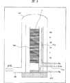
次に、図2に示すように、半導体基板1上に、n型の導電型を有する不純物、たとえばPH3が添加された多結晶シリコン膜6をCVD法(化学的成膜手段)で堆積する。この多結晶シリコン膜6の堆積は、たとえば図3に示すようなバッチ式の低圧CVD装置(第1成膜装置)を用いて行うことができる。この低圧CVD装置は、半導体基板1を保持するウェハホルダWHを処理室DC内に有している。処理室DC内へは、チューブTU1を通してSiH4ガスが供給され、このSiH4ガスの熱分解により多結晶シリコン膜6を形成することができる。また、チューブTU2、TU3よりPH3ガスを処理室DC内へ供給することにより、多結晶シリコン膜6にPH3を添加することができる。処理室DC内へ共給されたSiH4ガスおよびPH3ガスは排気口EXより排気することができる。また、図中の記号UU、U、CU、CL、LおよびLLは、処理室DC内において半導体基板1が保持されている高さを示す指標である。
本実施の形態1においては、図4に示すタイムチャートに沿って多結晶シリコン膜6の成膜を行うものである。図中のTは、成膜開始前における処理室DC内の加熱に要する時間であり、処理室DC内の容量によって規定することができる。また、Aは半導体基板1を処理室DC内に挿入後、大気圧下での処理室DC内の加熱に要する時間であり、Bは処理室DC内を真空または大気圧以下とした状況下での加熱工程に要する時間であり、前記TはAとBとの和で規定される。
上記多結晶シリコン膜6は、半導体基板1上のみならず、図3に示した処理室DCの内壁および処理室DC内におけるチューブTU1、TU2、TU3上にも成膜してしまう。また、このCVD装置は、多結晶シリコン膜6の成膜に繰り返し用いるものであり、新たな半導体基板1を処理室DC内に挿入した時には、処理室DC内の各所に多結晶シリコン膜6が成膜された状態となっている。この状況下で、長時間処理室DC内を真空または大気圧以下として加熱すると、処理室DC内の各所に成膜されている多結晶シリコン膜6が含むPH3がその多結晶シリコン膜6から拡散する。そのPH3は、半導体基板1上に形成されているゲート酸化膜5に導入され、ゲート酸化膜5の絶縁特性を劣化させてしまう恐れがある。
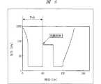
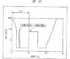
ここで、本発明者らの行った実験によれば、上記AおよびBの関係が0.1×B≦A≦13×Bとなる条件下で上記加熱工程を行うことにより、処理室DC内の各所に成膜されている多結晶シリコン膜6が含むPH3の拡散を抑制できることがわかった。また、本発明者らは、容量が約56lである処理室DCを有するCVD装置を用い、AおよびBを、それぞれ約45分および約15分と上記条件を満たすように規定し、半導体基板1の主面を296の領域に分割して各領域におけるゲート絶縁膜5の絶縁特性の劣化を調べる実験を行った。すなわち、分割した各々の領域のゲート絶縁膜5に対して電圧Vgを印加し、流れた電流Igを測定するものである。なお、容量が約56lである処理室DCの場合、上記Tは約60分で規定される。その結果、図5(a)に示すように、半導体基板1が保持されている高さがUU(図3参照)の場合には、296の領域のうち3の領域のみで絶縁特性の劣化が検出されるにとどまった。また、半導体基板1が保持されている高さがCL(図3参照)の場合には、図5(b)に示すように、296の領域のうち8の領域のみで絶縁特性の劣化が検出されるにとどまった。なお、図5中で“A”または“D”で示されている箇所は絶縁特性の劣化が検出された領域であり、“/”で示されている箇所は絶縁特性の劣化が検出されなかった領域である。すなわち、上記の条件のように、大気圧下での処理室DC内の加熱に要する時間Aに対して、処理室DC内を真空または大気圧以下とした状況下での加熱に要する時間Bを極力短くして処理室DC内へ加熱した後に多結晶シリコン膜6を成膜することにより、処理室DC内における半導体基板1が保持されている高さによらず、ゲート酸化膜5の絶縁特性の劣化を効果的に防ぐことができる。
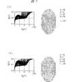
一方、図6に示すタイムチャートのように、T=Bとし、前記Aで規定した大気圧下での処理室DC内の加熱工程を行わない場合には、Bで規定される加熱工程の開始当初より処理室DC内の各所に成膜されている多結晶シリコン膜6よりPH3が拡散する。そのため、そのPH3が半導体基板1上に形成されているゲート酸化膜5に導入され、ゲート酸化膜5の絶縁特性を劣化させてしまう。本発明者らは、この条件下において、図5を用いて前述した実験と同様の実験を行った。その結果、図7(a)に示すように、半導体基板1が保持されている高さがUU(図3参照)の場合には、296の領域のうち162の領域で絶縁特性の劣化が検出された。半導体基板1が保持されている高さがCL(図3参照)の場合には、図7(b)に示すように、296の領域のうち140の領域で絶縁特性の劣化が検出された。なお、図7中で“A”、“C”または“D”で示されている箇所は絶縁特性の劣化が検出された領域であり、“/”で示されている箇所は絶縁特性の劣化が検出されなかった領域である。すなわち、図5に示した実験結果と合わせて、半導体基板1を処理室DC内に挿入後、大気圧下で処理室DC内を加熱することにより、処理室DC内の各所に成膜されている多結晶シリコン膜6からのPH3の拡散を効果的に防ぐことができることを確認でき、これにより、ゲート酸化膜5の絶縁特性の劣化を効果的に防ぐことが可能となる。
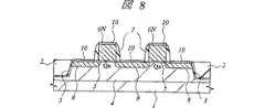
次に、図8に示すように、フォトリソグラフィ技術によりパターニングされたフォトレジスト膜(図示は省略)をマスクにして、多結晶シリコン膜6をドライエッチングすることにより、ゲート電極6Nを形成する。
続いて、上記フォトレジスト膜を除去した後、CVD法により半導体基板1上に酸化シリコン膜を堆積した後、反応性イオンエッチング(RIE)法でこの酸化シリコン膜を異方性エッチングすることにより、ゲート電極6Nの側壁にサイドウォールスペーサ7を形成する。次いで、n型の導電型を有する不純物(たとえばP)をイオン注入することにより、ゲート電極6Nの両側のp型ウェル4にnチャネルMISFETのソース、ドレイン領域を構成するn型半導体領域8を形成する。なお、サイドウォールスペーサ7の形成前に低濃度のn型半導体領域を形成し、サイドウォールスペーサ7の形成後に高濃度のn型半導体領域を形成してもよい。ここまでの工程により、nチャネル型MISFETQnを形成することができる。
次に、半導体基板1の表面を洗浄した後、たとえばスパッタリング法により、半導体基板1上にCo(コバルト)膜(図示は省略)を堆積する。続いて、半導体基板1に約600℃の熱処理を施すことにより、n型半導体領域8およびゲート電極6NとCo膜との界面にシリサイド化反応を生じさせてCoSi2層10を形成する。このCoSi2層10を形成することにより、後の工程においてn型半導体領域8上に形成される配線と半導体基板1との間でアロイスパイクが発生することを防ぐことができる。
次いで、未反応のCo膜をエッチングにより除去した後、約700℃〜800℃の熱処理によりCoSi2層10を低抵抗化する。これにより、上記配線とn型半導体領域8との間の接触抵抗を低減することができる。
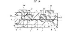
次に、図9に示すように、nチャネル型MISFETQnの上部に層間絶縁膜11を形成し、続いてフォトレジスト膜をマスクにして層間絶縁膜11をドライエッチングすることにより、n型半導体領域8の上部にスルーホール12を形成した後、層間絶縁膜11の上部に配線14を形成し、本実施の形態1の半導体集積回路装置を製造する。層間絶縁膜11は、たとえば酸化シリコン膜をCVD法にて堆積することによって形成する。また、配線14は、たとえば層間絶縁膜11の上部にスパッタリング法にてWあるいはAl合金などのメタル膜を堆積した後、フォトレジスト膜をマスクにしたドライエッチングでこのメタル膜をパターニングすることによって形成する。なお、上記層間絶縁膜11、スルーホール12および配線14を形成する工程を複数回繰り返すことによって、多層に配線を形成してもよい。
(実施の形態2)
本実施の形態2の半導体集積回路装置の製造方法は、前記実施の形態1において図4を用いて説明したタイムチャートとは異なるタイムチャートに沿って、多結晶シリコン膜6(図2参照)の成膜を行うものである。
本実施の形態2の半導体集積回路装置の製造方法は、前記実施の形態1において図1を用いて説明した工程までは同様である。その後、図3に示したCVD装置の処理室DC内に半導体基板1を挿入する。続いて、図10に示すタイムチャートに沿って多結晶シリコン膜6の成膜を行う。本実施の形態2においては、半導体基板1を処理室DC内に挿入直後より処理室DC内を真空または大気圧以下とし、処理室DC内への加熱を行う。多結晶シリコン膜6の成膜開始前における処理室DC内の加熱に要する時間Tは、前記実施の形態1の場合と同様であるが、このTで規定される加熱工程中に薄いノンドープの多結晶シリコン膜6の堆積を行う。これにより、ノンドープの多結晶シリコン膜6によりゲート酸化膜5を覆うことになり、処理室DC内を真空または大気圧以下として処理室DC内へ加熱し、処理室DC内の各所に成膜されている多結晶シリコン膜6が含むPH3がその多結晶シリコン膜6から拡散しても、ノンドープの多結晶シリコン膜6がゲート酸化膜5を保護し、そのPH3がゲート酸化膜5に導入されてしまうことを防ぐことができる。すなわち、ゲート酸化膜5の絶縁特性を劣化させてしまうことを防ぐことができる。本実施の形態2においては、このようなノンドープの多結晶シリコン膜6を形成した後、上記Tで規定される過熱工程を経てPH3が添加された多結晶シリコン膜6を堆積する。
その後、前記実施の形態1において、図8および図9を用いて説明した工程と同様の工程を経ることにより、本実施の形態2の半導体集積回路装置を製造する。
(実施の形態3)
以下、図11および図12を用いて本実施の形態3の半導体集積回路装置の製造方法について説明する。
本実施の形態3の半導体集積回路装置の製造方法は、前記実施の形態1において図1を用いて説明した工程までは同様である。その後、図11に示すように、前記実施の形態1において図3を用いて説明したCVD装置とは別の成膜装置(第2成膜装置)を用いて、半導体基板1上に薄いイントリンシックな多結晶シリコン膜6Aを堆積する。これにより、イントリンシックな多結晶シリコン膜6Aによりゲート酸化膜5を覆うことになる。すなわち、この後に前記実施の形態1において図3を用いて説明したようなCVD装置によりPH3が添加された多結晶シリコン膜6を堆積する際に、処理室DC内の各所に成膜されている多結晶シリコン膜6が含むPH3がその多結晶シリコン膜6から拡散しても、イントリンシックな多結晶シリコン膜6Aがゲート酸化膜5を保護し、そのPH3がゲート酸化膜5に導入されてしまうことを防ぐことができる。その結果、ゲート酸化膜5の絶縁特性を劣化させてしまうことを防ぐことができる。
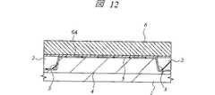
次に、図12に示すように、CVD法により上記イントリンシックな多結晶シリコン膜6A上に多結晶シリコン膜6を堆積した後、前記実施の形態1において図8および図9を用いて説明した工程と同様の工程を経ることにより、本実施の形態3の半導体集積回路装置を製造する。
(実施の形態4)
本実施の形態4は、前記実施の形態1をさらに詳細に補足説明するものである。
図13は、前記実施の形態1において図3を用いて説明した低圧CVD装置の構成をさらに詳細に示したものである。
図13に示すように、ウェハホルダWHは、処理室DCと処理室DCの下部に配置された搬送室TAとの間で昇降動作が可能な構造となっており、搬送室TA内にてウェハホルダWHに所定枚数の半導体基板1が配置された後、ウェハホルダWHは処理室DCへ上昇していく。半導体基板1上への多結晶シリコン膜6(半導体膜(図2参照))の成膜処理が終わると、ウェハホルダWHは再び搬送室TAへ下降していく。このように、本実施の形態の低圧CVD装置は、縦型構造の処理室DCを有している。
搬送室TA内には、ウェハカセットCAを配置するためのカセット棚CTが形成されている。ウェハカセットCAは、複数枚の半導体基板1を収納できるようになっている。また、本実施の形態において、搬送室TA内は、室温(約20℃)であるとする。
搬送室TA内では、搬送ロボットCRによってウェハホルダWHへの半導体基板1の配置、および多結晶シリコン膜6の成膜処理が終了した半導体基板1のウェハホルダWHからの取り出しが行われる。この搬送ロボットは、半導体基板1を裏面から吸着して搬送する搬送アームARMを複数本(たとえば5本)有し、昇降動作、水平動作および回転動作を行うことにより、ウェハカセットCAから一度に複数枚の半導体基板1を取り出し、その半導体基板1をウェハホルダWHへ配置する。所定枚数(たとえば、半導体基板1の径が約150mm(約6インチ)である場合には150枚程度)の半導体基板1がウェハホルダWHに配置されると、ウェハホルダWHは処理室DCへと上昇し、半導体基板1に対して多結晶シリコン膜6の成膜処理が施される。その多結晶シリコン膜6の成膜処理が終わり、ウェハホルダWHが搬送室TAへ下降すると、搬送ロボットCRはウェハホルダWHから半導体基板1を取り出し、ウェハカセットCAへ収納する。
処理室DCの外部には、処理室DCを加熱するためのヒーターH1、H2、H3、H4が設けられている。このヒーターH1、H2、H3、H4からの加熱により、処理室DC内は、常時500℃〜600℃程度に保たれている。
ヒーターH1、H2、H3、H4は、個別に加熱温度を設定することが可能であり、処理室DCへの加熱に温度勾配を形成することができる。たとえば、成膜ガスであるSiH4ガスおよびPH3ガスが処理室DCの下部から導入される場合には、相対的に処理室DCの下部に取り付けられたヒーターH4から相対的に処理室DCの上部に取り付けられたヒーター1に向かって、加熱温度が高くなるように各ヒーターの加熱温度を設定する。処理室DCの下部から導入された成膜ガスは、熱分解しながら上昇していく。そのため、成膜ガスは、処理室DCの上部に行くに従って熱分解し難くなる。つまり、半導体基板1上に上記多結晶シリコン膜6を堆積し難くなる。そこで、前述したように、ヒーター4からヒーター1に向かって加熱温度が高くなるように温度勾配を形成することによって、処理室DCの上部においても成膜ガスの熱分解を促進するものである。また、ヒーターH1、H2、H3、H4は、個別に加熱温度を設定することができるので、すべて同程度の温度で加熱することも可能である。
本実施の形態4では、処理室DCの外部に4個のヒーターH1、H2、H3、H4を取り付ける場合について例示したが、この4個のヒーターH1、H2、H3、H4にて加熱する場合と同様の加熱処理が可能な1個のヒーターまたは4個以外の複数個のヒーターを取り付ける構成としても良い。複数個のヒーターを取り付ける場合には、そのすべてが同じ大きさでなくても良い。
図14は、上記ウェハホルダWHへの半導体基板1の配置方法を示す説明図である。なお、図14においては、本実施の形態の半導体集積回路装置が実際に形成される(製品となる)半導体基板1については図示を省略している。
本実施の形態において、ウェハホルダWHには、径が約150mm(約6インチ)の半導体基板1が約150枚配置される。そのうち、たとえば最も下部に配置された20枚および最も上部に配置された5枚は、成膜処理中における、処理室DC内の成膜ガスを整流するために配置されたダミーウェハDWである。また、それら上部および下部のダミーウェハDWの間には、モニタ用ウェハMWが適当な間隔で複数枚(たとえば5枚程度)配置されている。このモニタ用ウェハMWは、上記多結晶シリコン膜6にドープされているPH3の濃度を測定する目的と、堆積された多結晶シリコン膜6の膜厚を測定するために配置されたものである。これらダミーウェハDWおよびモニタ用ウェハMWは、本実施の形態の半導体集積回路装置が実際に形成される半導体基板1とは別に用意されたものである。
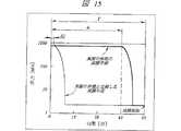
図15は、前記実施の形態1において図4および図6に示したタイムチャートのうち、多結晶シリコン膜6の成膜が開始するまでの処理室DC内の圧力変化を示したものであり、図16は、多結晶シリコン膜6の成膜が開始するまでの経過時間に対応した半導体基板1の温度変化を示したものである。図15に示した圧力変化および図16に示した温度変化は、ともにウェハホルダWHが処理室DC内に入りきった時点からのものを示している。なお、前記実施の形態1にて、図6に示したタイムチャートでは、ウェハホルダWHが処理室DC内に完全に入りきると同時に処理室DC内の減圧処理を開始する例を示しているが、実際には、ウェハホルダWHが処理室DC内に完全に入りきると同時に減圧処理を開始するつもりでも、多少の時間(たとえば数秒程度)が経過した後に減圧処理が始まることがほとんどなので、図15においては、その点も考慮した圧力変化を図示している。また、本実施の形態において、前述したヒーターH1、H2、H3、H4は、すべて同程度の温度で処理室DCを加熱し、処理室DCへの加熱に温度勾配は形成しないものとする。
図15には、処理室DC内の減圧処理を開始するまでに処理室DCに対して施した加熱処理時間について示している。Aは、本実施の形態の成膜手段におけるタイムチャート(前記実施の形態1にて示した図4に対応)のものであり、A1は、本実施の形態の成膜手段と比較した成膜手段におけるタイムチャート(前記実施の形態1にて示した図6に対応)のものである。
また、図16において示している半導体基板1の温度は、ウェハホルダWHに配置された半導体基板1のうち、最下部に配置された半導体基板(第1半導体基板)1の温度である。これは、ウェハホルダWHが処理室DC内に挿入される時に、ウェハホルダWHは上部から挿入されていくことと、上記したように処理室DC内は常時500℃〜600℃程度に加熱されていることから、相対的に上部に配置された半導体基板1は、ウェハホルダWHが処理室DCへ挿入されている途中でも加熱されていることに起因する。ウェハホルダWHの処理室DCへの挿入が完了した時点では、たとえば最上部の半導体基板1が約300℃で最下部の半導体基板1が約200℃というように温度差が生じており、ヒーターH1、H2、H3、H4からの加熱によって最上部の半導体基板1が成膜処理を開始できる温度に達した時点においても、最も温度の低い最下部の半導体基板1が成膜処理を開始できる温度に達していない場合が考えられる。すなわち、その最下部の半導体基板1が成膜処理を開始できる温度に達したことを確認することによって、ウェハホルダWHに配置されたすべての半導体基板1が成膜処理できる温度に達したと判断できるのである。なお、ヒーターH1、H2、H3、H4からの加熱に温度勾配を形成することによって、最下部の半導体基板1以外の半導体基板1が最も遅く成膜処理を開始できる温度に達するようになるならば、その最下部の半導体基板1以外の半導体基板1の温度変化を観察すればよい。
図15に示すように、本実施の形態の成膜手段においては、ウェハホルダWHを処理室DC内に挿入した後、半導体基板1が成膜処理を開始できる温度(第1の温度(たとえば約500℃))の約90%以上にまで加熱されてから処理室DC内の減圧処理を開始している。本実施の形態において、この約90%以上というのは、摂氏温度での値をもとにする。また、前述したように処理室DC内は常時500℃〜600℃程度に加熱されており、この加熱温度は半導体基板1の温度を成膜処理を行える温度に保持できるように設定されていることから、半導体基板1の温度変化は、成膜処理を開始できる温度に達すると安定する。なお、減圧処理を開始するまでは、処理室DC内の圧力は大気圧(第1気圧)に保たれている。すなわち、処理室DC内は成膜処理を行なう圧力(第3気圧)以上の圧力(第1気圧)に保たれている。
ここで、ウェハホルダWHが処理室DC内に挿入された後、処理室DC内の減圧処理を開始するまでの時間がAである。また、処理室DC内の減圧処理は、処理室DC内が成膜処理を行える圧力になった時点で停止し、処理室DC内をその圧力で保持するものである。すなわち、処理室DC内を成膜処理を行なう圧力(第3気圧)以下の圧力(第2気圧)まで減圧した後、処理室DC内に成膜のための成膜ガスを供給し成膜を行なう圧力で成膜処理を行なう。
一方、本実施の形態の成膜手段と比較した成膜手段の場合には、ウェハホルダWHが処理室DC内に挿入された後、処理室DC内の減圧処理を開始するまでに多少のインターバル時間A1があるものの、ほぼウェハホルダWHが処理室DC内に挿入された直後から処理室DC内の減圧処理を開始している。つまり、半導体基板1の温度が成膜処理を開始できる温度に達する前に処理室DC内の減圧処理を行っている。そのため、本実施の形態の成膜手段に比べて、真空に近い状態処理室DC内で半導体基板1は加熱されることになるので、本実施の形態1の成膜手段に比べて半導体基板1の温度は上昇し難くなる(図16参照)。なお、本実施の形態の成膜手段と同様に、処理室DC内の減圧処理は、処理室DC内が成膜処理を行える圧力になった時点で停止し、処理室DC内をその圧力で保持するものである。
ところで、本実施の形態の成膜手段および本実施の形態の成膜手段と比較した成膜手段共に、処理室DC内の減圧処理は、処理室DC内に異物が発生しない程度に可能な限り短時間で行っている。これは、減圧処理中に他の処理を行った場合には、処理室DC内に異物等を巻き込んでしまう恐れがあるからであり、処理室DC内に異物等を巻き込んでしまった場合には、成膜される多結晶シリコン膜6の膜質を低下させてしまうことが懸念されるからである。
以上、本発明者によってなされた発明を発明の実施の形態に基づき具体的に説明したが、本発明は前記実施の形態に限定されるものではなく、その要旨を逸脱しない範囲で種々変更可能であることは言うまでもない。
たとえば、前記実施の形態においては、多結晶シリコン膜にPH3を添加する場合について示したが、AsH3を添加してもよい。
また、前記実施の形態においてはnチャネル型MISFETを形成する場合について示したが、pチャネル型MISFETを形成する場合にも本発明の半導体集積回路装置の製造方法は適用可能であり、この場合には、ゲート電極となる多結晶シリコン膜にはB2H6などを添加する。
また、前記実施の形態の多結晶シリコン膜の成膜方法は、ゲート電極材料となる多結晶シリコン膜の成膜ばかりでなく、MOSキャパシタの容量電極あるいはDRAMのキャパシタの下部電極となる多結晶シリコン膜の成膜にも適用することが可能である。
産業上の利用可能性
本発明は、MISFET、DRAM(Dynamic Random Access Memory)を始めとする半導体集積回路装置の製造工程およびマイクロマシンの製造工程などに適用することができる。
【図面の簡単な説明】
図1は、本発明の一実施の形態である半導体集積回路装置の製造方法を示す要部断面図である。
図2は、図1に続く半導体集積回路装置の製造工程中の要部断面図である。
図3は、本発明の一実施の形態である半導体集積回路装置の製造に用いるCVD装置の構成を説明する説明図である。
図4は、本発明の一実施の形態である半導体集積回路装置の製造工程中における多結晶シリコン膜の堆積時のタイムチャートである。
図5は、本発明の一実施の形態である半導体集積回路装置の製造方法により多結晶シリコン膜を形成した場合におけるゲート酸化膜の絶縁特性を示す説明図である。
図6は、本発明の一実施の形態である半導体集積回路装置の製造工程と比較した製造工程による多結晶シリコン膜の堆積時のタイムチャートである。
図7は、本発明の一実施の形態である半導体集積回路装置の製造工程と比較した製造工程により多結晶シリコン膜を形成した場合におけるゲート酸化膜の絶縁特性を示す説明図である。
図8は、図2に続く半導体集積回路装置の製造工程中の要部断面図である。
図9は、図8に続く半導体集積回路装置の製造工程中の要部断面図である。
図10は、本発明の他の実施の形態である半導体集積回路装置の製造工程中における多結晶シリコン膜の堆積時のタイムチャートである。
図11は、本発明の他の実施の形態である半導体集積回路装置の製造方法を示す要部断面図である。
図12は、図11に続く半導体集積回路装置の製造工程中の要部断面図である。
図13は、本発明の他の実施の形態である半導体集積回路装置の製造に用いるCVD装置の構成を説明する説明図である。
図14は、図13に示したCVD装置が有するウェハホルダおよびウェハホルダに配置された半導体基板の構成を示す説明図である。
図15は、本発明の他の実施の形態である半導体集積回路装置の製造工程中における多結晶シリコン膜の堆積時の処理室内の圧力変化を示すタイムチャートである。
図16は、本発明の他の実施の形態である半導体集積回路装置の製造工程中における多結晶シリコン膜の堆積時の処理室内の温度変化を示すタイムチャートである。Technical field
The present invention relates to a manufacturing technique of a semiconductor integrated circuit device, and more particularly to an effective technique applied to a process of depositing a silicon film into which impurity ions are introduced by a CVD (Chemical Vapor Deposition) method.
Background art
As a gate electrode material of a MISFET (Metal Insulator Semiconductor Field Effect Transistor), for example, a polycrystalline silicon film to which an impurity is added is used. At this time, as an impurity to be added, in the case of an n-channel MISFET, AsH3 Or PH3 Can be used, and in the case of a p-channel MISFET, B2 H6 Etc. can be used.
Such a polycrystalline silicon film can be formed using, for example, a low-pressure CVD apparatus. Here, the low-pressure CVD apparatus is described in November 20, 1997, edited by Japan Semiconductor Manufacturing Equipment Association, published by Nikkan Kogyo Shimbun, “Semiconductor Manufacturing Equipment Glossary 4th Edition”, p187.
However, the present inventors have found that the low-pressure CVD apparatus as described above has the following problems.
That is, when a polycrystalline silicon film doped with impurities as described above is formed as a gate electrode material of a MISFET by a low-pressure CVD apparatus, after the semiconductor wafer is inserted into the processing chamber, the processing chamber is evacuated or atmospheric pressure. Under the conditions described below, the process waits for a certain period of time until the temperature in the processing chamber rises, and then a film is formed by introducing the generated gas into the processing chamber. At this time, the polycrystalline silicon film is deposited not only on the surface of the semiconductor wafer but also on the inner wall of the processing chamber. Subsequently, in the case where a similar polycrystalline silicon film is formed on a new semiconductor wafer, the temperature in the processing chamber rises in a state where the processing chamber is evacuated or under atmospheric pressure in the same process. While waiting for a certain time, impurities diffuse from the polycrystalline silicon film formed on the inner wall of the processing chamber. The diffused impurities are scattered on the semiconductor wafer before the polycrystalline silicon film is formed and are introduced into the gate oxide film previously formed on the surface of the semiconductor wafer. There is a problem of degrading.
It is an object of the present invention to suppress diffusion of impurities from a similar polycrystalline silicon film formed on a processing chamber wall when forming a polycrystalline silicon film to which impurities are added by a low pressure CVD apparatus. Is to provide.
The above and other objects and novel features of the present invention will be apparent from the description of this specification and the accompanying drawings.
Disclosure of the invention
Of the inventions disclosed in the present application, the outline of typical ones will be briefly described as follows.
That is, the present invention provides a step of inserting a semiconductor substrate into a processing chamber of a first film forming apparatus, a step of heating the processing chamber, and a conductive film formed on the semiconductor substrate by chemical film forming means after the heating step. Forming a silicon film to which an impurity having a property is added, and the heating step includes:
(A) maintaining the inside of the processing chamber at atmospheric pressure and heating the processing chamber;
(B) After the step (a), the step of heating the processing chamber in a state where the processing chamber is set to a vacuum or atmospheric pressure or less, and the time required for the step (a) is required for the step (b). It is longer than time.
According to the present invention, after an insulating film is formed on the semiconductor substrate, the semiconductor substrate is inserted into a processing chamber of the first film forming apparatus, and the semiconductor substrate is heated while maintaining the atmospheric pressure in the processing chamber. And after the step of heating the semiconductor substrate, the step of reducing the pressure in the processing chamber to a vacuum or atmospheric pressure or lower while heating the semiconductor substrate, and the pressure in the processing chamber to a vacuum or atmospheric pressure or lower. Forming a semiconductor film to which an impurity having conductivity is added on the insulating film by a chemical film forming means, and heating the semiconductor substrate while maintaining the processing chamber at atmospheric pressure The heating is performed to bring the temperature of the semiconductor substrate to the first temperature of the semiconductor substrate during the formation of the semiconductor film, or to bring the temperature of the semiconductor substrate close to the first temperature.
According to another aspect of the present invention, there is provided a step of forming an insulating film on a semiconductor substrate, a step of inserting the semiconductor substrate into a processing chamber of a first film forming apparatus, maintaining the processing chamber at a first atmospheric pressure, A step of heating to a first temperature, a step of reducing the pressure in the processing chamber to a second atmospheric pressure or lower while heating the semiconductor substrate, and a third of the pressure in the processing chamber being a vacuum or an atmospheric pressure or lower. Forming a silicon film to which an impurity having conductivity is added on the insulating film of the semiconductor substrate at the first temperature by using a chemical film-forming means while maintaining the pressure. The pressure is reduced so that the atmospheric pressure is lower than the third atmospheric pressure, and the first atmospheric pressure is higher than the third atmospheric pressure.
According to another aspect of the present invention, there is provided a step of forming an insulating film on a semiconductor substrate, a step of inserting the semiconductor substrate into a processing chamber of a first film forming apparatus, maintaining the processing chamber at a first atmospheric pressure, A step of heating, a step of reducing the pressure in the processing chamber to a second atmospheric pressure or lower while heating the semiconductor substrate, and maintaining the pressure in the processing chamber at a vacuum or a third atmospheric pressure of atmospheric pressure or lower. Forming a silicon film to which a conductive impurity is added on the insulating film by a film forming means, and reducing the second atmospheric pressure to be lower than the third atmospheric pressure, In the film forming step, heating is performed so that the temperature of the semiconductor substrate approaches the first temperature while maintaining the first pressure higher than the third pressure.
BEST MODE FOR CARRYING OUT THE INVENTION
DESCRIPTION OF THE PREFERRED EMBODIMENTS Embodiments of the present invention will be described in detail below with reference to the drawings. (In the drawings for explaining the embodiments, components having the same functions are denoted by the same reference numerals, and repeated description thereof is omitted.) To do).
(Embodiment 1)
Hereinafter, a method for manufacturing the semiconductor integrated circuit device according to the first embodiment will be described with reference to FIGS.
First, as shown in FIG. 1, a
Subsequently, a groove having a depth of about 350 nm is formed in the
Subsequently, after the
Next, after the silicon nitride film remaining on the active region of the
Next, as shown in FIG. 2, an impurity having an n-type conductivity, such as PH, is formed on the
In the first embodiment, the
The
Here, according to an experiment conducted by the present inventors, the heating step is performed under the condition that the relationship between A and B is 0.1 × B ≦ A ≦ 13 × B, so that the inside of the processing chamber DC is PH included in the
On the other hand, as shown in the time chart of FIG. 6, when T = B and the heating process in the processing chamber DC under the atmospheric pressure defined by A is not performed, the heating process defined by B is started. PH from the
Next, as shown in FIG. 8, a
Subsequently, after removing the photoresist film, a silicon oxide film is deposited on the
Next, after cleaning the surface of the
Next, after removing the unreacted Co film by etching, the CoSi is heat-treated at about 700 ° C. to 800 ° C.2 The resistance of the
Next, as shown in FIG. 9, the interlayer insulating film 11 is formed on the n-channel type MISFET Qn, and then the interlayer insulating film 11 is dry-etched using the photoresist film as a mask, thereby forming the n-
(Embodiment 2)
The manufacturing method of the semiconductor integrated circuit device according to the second embodiment is performed on the polycrystalline silicon film 6 (see FIG. 2) along a time chart different from the time chart described with reference to FIG. 4 in the first embodiment. A film is formed.
The manufacturing method of the semiconductor integrated circuit device according to the second embodiment is the same up to the steps described with reference to FIG. 1 in the first embodiment. Thereafter, the
Thereafter, in the first embodiment, the semiconductor integrated circuit device of the second embodiment is manufactured through the same steps as those described with reference to FIGS.
(Embodiment 3)
A method for manufacturing the semiconductor integrated circuit device according to the third embodiment will be described below with reference to FIGS.
The manufacturing method of the semiconductor integrated circuit device of the third embodiment is the same up to the process described with reference to FIG. 1 in the first embodiment. Thereafter, as shown in FIG. 11, a thin intrinsic layer is formed on the
Next, as shown in FIG. 12, after depositing the
(Embodiment 4)
The fourth embodiment supplements the first embodiment in more detail.
FIG. 13 shows in more detail the configuration of the low-pressure CVD apparatus described with reference to FIG. 3 in the first embodiment.
As shown in FIG. 13, the wafer holder WH has a structure capable of moving up and down between the processing chamber DC and the transfer chamber TA disposed below the processing chamber DC, and the wafer holder WH in the transfer chamber TA. After the predetermined number of
A cassette shelf CT for arranging the wafer cassette CA is formed in the transfer chamber TA. The wafer cassette CA can store a plurality of
In the transfer chamber TA, the arrangement of the
Heaters H1, H2, H3, and H4 for heating the processing chamber DC are provided outside the processing chamber DC. By heating from the heaters H1, H2, H3, and H4, the inside of the processing chamber DC is always kept at about 500 ° C. to 600 ° C.
The heaters H1, H2, H3, and H4 can individually set the heating temperature, and can form a temperature gradient in heating the processing chamber DC. For example, SiH which is a film forming gas4 Gas and PH3 When the gas is introduced from the lower part of the processing chamber DC, the heating temperature moves from the heater H4 relatively attached to the lower part of the processing chamber DC toward the
In the fourth embodiment, the case where the four heaters H1, H2, H3, and H4 are attached to the outside of the processing chamber DC is exemplified. However, the case where the four heaters H1, H2, H3, and H4 are used for heating. One heater or a plurality of heaters other than four that can be similarly heat-treated may be attached. When installing a plurality of heaters, all of them need not be the same size.
FIG. 14 is an explanatory view showing a method of arranging the
In the present embodiment, about 150
FIG. 15 shows the pressure change in the processing chamber DC until the deposition of the
FIG. 15 shows the heat treatment time applied to the processing chamber DC until the decompression processing in the processing chamber DC is started. A is a time chart (corresponding to FIG. 4 shown in the first embodiment) in the film formation means of the present embodiment, and A1 is a film formation compared with the film formation means of the present embodiment. 7 is a time chart of the means (corresponding to FIG. 6 shown in the first embodiment).
Further, the temperature of the
As shown in FIG. 15, in the film forming means of the present embodiment, after the wafer holder WH is inserted into the processing chamber DC, the temperature at which the
Here, after the wafer holder WH is inserted into the processing chamber DC, the time until the decompression processing in the processing chamber DC is started is A. Further, the decompression process in the processing chamber DC is stopped when the pressure in the processing chamber DC reaches a pressure at which a film forming process can be performed, and the processing chamber DC is held at the pressure. That is, after reducing the pressure in the processing chamber DC to a pressure (second atmospheric pressure) that is equal to or lower than the pressure (third atmospheric pressure) for performing the film forming processing, a film forming gas is supplied into the processing chamber DC to form a film. The film forming process is performed at the pressure to be performed.
On the other hand, in the case of the film forming unit compared with the film forming unit of the present embodiment, after the wafer holder WH is inserted into the processing chamber DC, a certain interval time is required until the decompression processing in the processing chamber DC is started. Although there is A1, the decompression processing in the processing chamber DC is started almost immediately after the wafer holder WH is inserted into the processing chamber DC. That is, the decompression process in the processing chamber DC is performed before the temperature of the
By the way, both the film forming unit of the present embodiment and the film forming unit compared with the film forming unit of the present embodiment, the decompression process in the processing chamber DC is as much as possible to the extent that no foreign matter is generated in the processing chamber DC. It takes a short time. This is because if other processing is performed during the decompression processing, foreign matter or the like may be caught in the processing chamber DC, and if foreign matter or the like is caught in the processing chamber DC. This is because there is a concern that the film quality of the
As mentioned above, the invention made by the present inventor has been specifically described based on the embodiments of the invention. However, the present invention is not limited to the above-described embodiments, and various modifications can be made without departing from the scope of the invention. Needless to say.
For example, in the above-described embodiment, the polycrystalline silicon film is PH.3 As shown in the case of adding AsH3 May be added.
Further, although the case where the n-channel type MISFET is formed has been described in the above embodiment, the method for manufacturing the semiconductor integrated circuit device of the present invention can be applied to the case where the p-channel type MISFET is formed. Has a B on the polycrystalline silicon film to be the gate electrode.2 H6 Etc. are added.
Further, the polycrystalline silicon film forming method of the above embodiment is not limited to the formation of the polycrystalline silicon film as the gate electrode material, but the polycrystalline silicon used as the capacitor electrode of the MOS capacitor or the lower electrode of the DRAM capacitor. The present invention can also be applied to film formation.
Industrial applicability
The present invention can be applied to a manufacturing process of a semiconductor integrated circuit device such as a MISFET and a DRAM (Dynamic Random Access Memory) and a manufacturing process of a micromachine.
[Brief description of the drawings]
FIG. 1 is a fragmentary cross-sectional view showing a method for manufacturing a semiconductor integrated circuit device according to an embodiment of the present invention.
2 is a fragmentary cross-sectional view of the semiconductor integrated circuit device during a manufacturing step following that of FIG.
FIG. 3 is an explanatory diagram for explaining the configuration of a CVD apparatus used for manufacturing a semiconductor integrated circuit device according to an embodiment of the present invention.
FIG. 4 is a time chart when the polycrystalline silicon film is deposited during the manufacturing process of the semiconductor integrated circuit device according to the embodiment of the present invention.
FIG. 5 is an explanatory diagram showing the insulating characteristics of the gate oxide film when a polycrystalline silicon film is formed by the method for manufacturing a semiconductor integrated circuit device according to one embodiment of the present invention.
FIG. 6 is a time chart when the polycrystalline silicon film is deposited by the manufacturing process compared to the manufacturing process of the semiconductor integrated circuit device according to the embodiment of the present invention.
FIG. 7 is an explanatory diagram showing the insulation characteristics of the gate oxide film when a polycrystalline silicon film is formed by a manufacturing process compared with the manufacturing process of the semiconductor integrated circuit device according to one embodiment of the present invention.
FIG. 8 is a fragmentary cross-sectional view of the semiconductor integrated circuit device during a manufacturing step following that of FIG.
FIG. 9 is a fragmentary cross-sectional view of the semiconductor integrated circuit device during a manufacturing step following that of FIG. 8.
FIG. 10 is a time chart when the polycrystalline silicon film is deposited during the manufacturing process of the semiconductor integrated circuit device according to another embodiment of the present invention.
FIG. 11 is a fragmentary sectional view showing a method for manufacturing a semiconductor integrated circuit device according to another embodiment of the present invention.
FIG. 12 is a fragmentary cross-sectional view of the semiconductor integrated circuit device during a manufacturing step following that of FIG. 11.
FIG. 13 is an explanatory view illustrating the configuration of a CVD apparatus used for manufacturing a semiconductor integrated circuit device according to another embodiment of the present invention.
FIG. 14 is an explanatory diagram illustrating a configuration of a wafer holder included in the CVD apparatus illustrated in FIG. 13 and a semiconductor substrate disposed on the wafer holder.
FIG. 15 is a time chart showing a pressure change in the processing chamber during the deposition of the polycrystalline silicon film during the manufacturing process of the semiconductor integrated circuit device according to another embodiment of the present invention.
FIG. 16 is a time chart showing a temperature change in the processing chamber during the deposition of the polycrystalline silicon film during the manufacturing process of the semiconductor integrated circuit device according to another embodiment of the present invention.
Claims (13)
Translated fromJapanese(b)前記(a)工程後、前記半導体基板を第1成膜装置の処理室内に挿入する工程と、
(c)前記処理室内に加熱する工程と、
(d)前記(c)工程後、化学的成膜手段にて前記絶縁膜上に導電性を有する不純物が添加されたシリコン膜を成膜する工程とを含み、
前記(c)工程は、
(c1)前記処理室内を大気圧に保ち、前記処理室内に加熱する工程と、
(c2)前記(c1)工程後、前記処理室内を真空または大気圧以下とした状態で前記処理室内に加熱する工程とを含み、
前記(c1)工程に要する時間は前記(c2)工程に要する時間よりも長いことを特徴とする半導体集積回路装置の製造方法。(A) forming an insulating film on the semiconductor substrate;
(B) After the step (a), inserting the semiconductor substrate into a processing chamber of the first film forming apparatus;
(C) heating the processing chamber;
(D) after the step (c), forming a silicon film to which an impurity having conductivity is added on the insulating film by a chemical film forming means,
The step (c)
(C1) maintaining the inside of the processing chamber at atmospheric pressure and heating the processing chamber;
(C2) after the step (c1), heating the processing chamber in a state where the processing chamber is in a vacuum or atmospheric pressure or less,
A method of manufacturing a semiconductor integrated circuit device, wherein a time required for the step (c1) is longer than a time required for the step (c2).
(b)前記(a)工程後、前記半導体基板を第1成膜装置の処理室内に挿入する工程と、
(c)前記処理室内に加熱する工程と、
(d)前記(c)工程後、化学的成膜手段にて前記絶縁膜上に導電性を有する不純物が添加されたシリコン膜を成膜する工程とを含み、
前記(c)工程は、
(c1)前記処理室内を大気圧に保ち、前記処理室内に加熱する工程と、
(c2)前記(c1)工程後、前記処理室内を真空または大気圧以下とした状態で前記処理室内に加熱する工程を含み、
前記(c1)工程に要する時間は前記(c2)工程に要する時間の0.1倍以上かつ13倍以下であることを特徴とする半導体集積回路装置の製造方法。(A) forming an insulating film on the semiconductor substrate;
(B) After the step (a), inserting the semiconductor substrate into a processing chamber of the first film forming apparatus;
(C) heating the processing chamber;
(D) after the step (c), forming a silicon film to which an impurity having conductivity is added on the insulating film by a chemical film forming means,
The step (c)
(C1) maintaining the inside of the processing chamber at atmospheric pressure and heating the processing chamber;
(C2) after the step (c1), including a step of heating the processing chamber in a state where the processing chamber is vacuum or atmospheric pressure or lower,
The time required for the step (c1) is 0.1 to 13 times the time required for the step (c2).
(b)前記(a)工程後、前記半導体基板を第1成膜装置の処理室内に挿入する工程と、
(c)前記処理室内を真空または大気圧以下とする工程と、
(d)前記(c)工程後、化学的成膜手段にて前記絶縁膜上に導電性を有する不純物を含まないシリコン膜を成膜する工程と、
(e)前記(d)工程後、前記処理室内を真空または大気圧以下とした状態で前記処理室内に加熱する工程と、
(f)前記(e)工程後、化学的成膜手段にて前記シリコン膜上に導電性を有する不純物が添加されたシリコン膜を成膜する工程とを含み、
前記(c)工程に要する時間は前記(e)工程に要する時間よりも短いことを特徴とする半導体集積回路装置の製造方法。(A) forming an insulating film on the semiconductor substrate;
(B) After the step (a), inserting the semiconductor substrate into a processing chamber of the first film forming apparatus;
(C) a step of setting the processing chamber to a vacuum or an atmospheric pressure or lower;
(D) After the step (c), a step of forming a silicon film containing no conductive impurities on the insulating film by chemical film formation means;
(E) after the step (d), heating the processing chamber in a state where the processing chamber is in a vacuum or atmospheric pressure or less;
(F) After the step (e), a step of forming a silicon film to which an impurity having conductivity is added on the silicon film by a chemical film forming means,
A method of manufacturing a semiconductor integrated circuit device, wherein a time required for the step (c) is shorter than a time required for the step (e).
(b)前記(a)工程後、第2成膜装置を用い化学的成膜手段にて前記絶縁膜上に導電性を有する不純物を含まないシリコン膜を成膜する工程と、
(c)前記(b)工程後、第1成膜装置を用い化学的成膜手段にて前記シリコン膜上に導電性を有する不純物が添加されたシリコン膜を成膜する工程とを含むことを特徴とする半導体集積回路装置の製造方法。(A) forming an insulating film on the semiconductor substrate;
(B) After the step (a), a step of forming a silicon film not containing impurities having conductivity on the insulating film by a chemical film forming unit using a second film forming apparatus;
(C) After the step (b), a step of forming a silicon film to which an impurity having conductivity is added on the silicon film by a chemical film forming unit using a first film forming apparatus is included. A method of manufacturing a semiconductor integrated circuit device.
(b)前記(a)工程後、前記半導体基板を第1成膜装置の処理室内に挿入する工程と、
(c)前記処理室内を大気圧に保ち、前記半導体基板を加熱する工程と、
(d)前記(c)工程後、前記半導体基板を加熱しつつ前記処理室内の圧力を真空または大気圧以下に減圧する工程、
(e)前記処理室内の前記圧力を真空または大気圧以下に保ち、化学的成膜手段にて前記絶縁膜上に導電性を有する不純物が添加された半導体膜を成膜する工程とを含み、
前記(c)工程では、前記半導体基板の温度を前記半導体膜の成膜時における前記半導体基板の第1の温度にする加熱、または前記半導体基板の温度を前記第1の温度に近づける加熱を行うことを特徴とする半導体集積回路装置の製造方法。(A) forming an insulating film on the semiconductor substrate;
(B) After the step (a), inserting the semiconductor substrate into a processing chamber of the first film forming apparatus;
(C) maintaining the inside of the processing chamber at atmospheric pressure and heating the semiconductor substrate;
(D) After the step (c), a step of reducing the pressure in the processing chamber to a vacuum or an atmospheric pressure or lower while heating the semiconductor substrate;
(E) maintaining the pressure in the processing chamber at a vacuum or lower than atmospheric pressure and forming a semiconductor film to which a conductive impurity is added on the insulating film by chemical film forming means,
In the step (c), heating is performed to bring the temperature of the semiconductor substrate to the first temperature of the semiconductor substrate at the time of forming the semiconductor film, or to bring the temperature of the semiconductor substrate close to the first temperature. A method of manufacturing a semiconductor integrated circuit device.
(b)前記(a)工程後、前記半導体基板を第1成膜装置の処理室内に挿入する工程と、
(c)前記処理室内を大気圧に保ち、前記半導体基板を加熱する工程と、
(d)前記(c)工程後、前記半導体基板を加熱しつつ前記処理室内の圧力を真空または大気圧以下に減圧する工程、
(e)前記処理室内の前記圧力を真空または大気圧以下に保ち、化学的成膜手段にて前記絶縁膜上に導電性を有する不純物が添加された半導体膜を成膜する工程とを含み、
前記処理室内には複数枚の前記半導体基板が配置され、前記処理室は複数枚の前記半導体基板が上下方向に並べて配置される縦型の処理室であり、前記(c)工程では、前記半導体基板の温度を前記半導体膜の成膜時における前記半導体基板の第1の温度にする加熱、または前記半導体基板の温度を前記第1の温度に近づける加熱を行うことを特徴とする半導体集積回路装置の製造方法。(A) forming an insulating film on the semiconductor substrate;
(B) After the step (a), inserting the semiconductor substrate into a processing chamber of the first film forming apparatus;
(C) maintaining the inside of the processing chamber at atmospheric pressure and heating the semiconductor substrate;
(D) After the step (c), a step of reducing the pressure in the processing chamber to a vacuum or an atmospheric pressure or lower while heating the semiconductor substrate;
(E) maintaining the pressure in the processing chamber at a vacuum or lower than atmospheric pressure and forming a semiconductor film to which a conductive impurity is added on the insulating film by chemical film forming means,
A plurality of the semiconductor substrates are disposed in the processing chamber, and the processing chamber is a vertical processing chamber in which the plurality of semiconductor substrates are arranged in the vertical direction. In the step (c), the semiconductor Heating to bring the temperature of the substrate to the first temperature of the semiconductor substrate when forming the semiconductor film or heating to bring the temperature of the semiconductor substrate to the first temperature is performed. Manufacturing method.
(b)前記(a)工程後、前記半導体基板を第1成膜装置の処理室内に挿入する工程と、
(c)前記処理室内を第1気圧に保ち、前記半導体基板を第1の温度に加熱する工程と、
(d)前記(c)工程後、前記半導体基板を加熱しつつ前記処理室内の圧力を第2気圧以下に減圧する工程、
(e)前記処理室内の前記圧力を真空または大気圧以下の第3気圧に保ち、化学的成膜手段にて、前記第1の温度の半導体基板の前記絶縁膜上に、導電性を有する不純物が添加されたシリコン膜を成膜する工程とを含み、
前記(d)工程は、前記第2気圧が前記第3気圧よりも低くなるように減圧し、
前記(c)工程は、前記第1気圧が前記第3気圧よりも高いことを特徴とする半導体集積回路装置の製造方法。(A) forming an insulating film on the semiconductor substrate;
(B) After the step (a), inserting the semiconductor substrate into a processing chamber of the first film forming apparatus;
(C) maintaining the process chamber at a first pressure and heating the semiconductor substrate to a first temperature;
(D) After the step (c), the step of reducing the pressure in the processing chamber to a second atmospheric pressure or lower while heating the semiconductor substrate;
(E) Impurities having conductivity on the insulating film of the semiconductor substrate at the first temperature by chemical film forming means while maintaining the pressure in the processing chamber at a vacuum or a third atmospheric pressure lower than atmospheric pressure. Forming a silicon film to which is added,
In the step (d), the pressure is reduced so that the second pressure is lower than the third pressure,
In the step (c), the first atmospheric pressure is higher than the third atmospheric pressure.
(b)前記(a)工程後、前記半導体基板を第1成膜装置の処理室内に挿入する工程と、
(c)前記処理室内を第1気圧に保ち、前記半導体基板を加熱する工程と、
(d)前記(c)工程後、前記半導体基板を加熱しつつ前記処理室内の圧力を第2気圧以下に減圧する工程、
(e)前記処理室内の前記圧力を真空または大気圧以下の第3気圧に保ち、化学的成膜手段にて前記絶縁膜上に導電性を有する不純物が添加されたシリコン膜を成膜する工程とを含み、
前記(d)工程は、前記第2気圧が前記第3気圧よりも低くなるように減圧し、
前記(c)工程は、前記第1気圧を、前記第3気圧よりも高い状態に保ちつつ、かつ、前記半導体基板の温度を前記第1の温度に近づける加熱を行うことを特徴とする半導体集積回路装置の製造方法。(A) forming an insulating film on the semiconductor substrate;
(B) After the step (a), inserting the semiconductor substrate into a processing chamber of the first film forming apparatus;
(C) maintaining the inside of the processing chamber at a first pressure and heating the semiconductor substrate;
(D) After the step (c), the step of reducing the pressure in the processing chamber to a second atmospheric pressure or lower while heating the semiconductor substrate;
(E) A step of forming a silicon film to which an impurity having conductivity is added on the insulating film by a chemical film forming means while keeping the pressure in the processing chamber at a vacuum or a third atmospheric pressure lower than atmospheric pressure. Including
In the step (d), the pressure is reduced so that the second pressure is lower than the third pressure,
In the step (c), the semiconductor integrated circuit is characterized in that the first atmospheric pressure is kept higher than the third atmospheric pressure, and heating is performed to bring the temperature of the semiconductor substrate close to the first temperature. A method of manufacturing a circuit device.
Applications Claiming Priority (3)
| Application Number | Priority Date | Filing Date | Title |
|---|---|---|---|
| JP2002002507 | 2002-01-09 | ||
| JP2002002507 | 2002-01-09 | ||
| PCT/JP2003/000068WO2003060970A1 (en) | 2002-01-09 | 2003-01-08 | Semiconductor integrated circuit device manufacturing method |
Publications (2)
| Publication Number | Publication Date |
|---|---|
| JPWO2003060970A1 JPWO2003060970A1 (en) | 2005-05-19 |
| JP4125239B2true JP4125239B2 (en) | 2008-07-30 |
Family
ID=19190754
Family Applications (1)
| Application Number | Title | Priority Date | Filing Date |
|---|---|---|---|
| JP2003560969AExpired - Fee RelatedJP4125239B2 (en) | 2002-01-09 | 2003-01-08 | Manufacturing method of semiconductor integrated circuit device |
Country Status (5)
| Country | Link |
|---|---|
| US (1) | US7163849B2 (en) |
| JP (1) | JP4125239B2 (en) |
| KR (1) | KR20040085145A (en) |
| CN (1) | CN1613142A (en) |
| WO (1) | WO2003060970A1 (en) |
Families Citing this family (1)
| Publication number | Priority date | Publication date | Assignee | Title |
|---|---|---|---|---|
| JP6017396B2 (en)* | 2012-12-18 | 2016-11-02 | 東京エレクトロン株式会社 | Thin film forming method and thin film forming apparatus |
Family Cites Families (8)
| Publication number | Priority date | Publication date | Assignee | Title |
|---|---|---|---|---|
| JPH05217910A (en) | 1992-02-05 | 1993-08-27 | Seiko Epson Corp | Compound semiconductor vapor phase growth apparatus and vapor phase growth method |
| JPH07230955A (en) | 1994-02-18 | 1995-08-29 | Hitachi Ltd | Vapor growth method and its apparatus |
| US6159300A (en)* | 1996-12-17 | 2000-12-12 | Canon Kabushiki Kaisha | Apparatus for forming non-single-crystal semiconductor thin film, method for forming non-single-crystal semiconductor thin film, and method for producing photovoltaic device |
| KR100305527B1 (en)* | 1998-07-09 | 2001-11-01 | 니시무로 타이죠 | Method and apparatus for manufactu ring semiconductor device |
| US6270580B2 (en)* | 1999-04-12 | 2001-08-07 | Advanced Micro Devices, Inc. | Modified material deposition sequence for reduced detect densities in semiconductor manufacturing |
| KR100757552B1 (en)* | 2000-07-25 | 2007-09-10 | 동경 엘렉트론 주식회사 | Heat processing unit, heat processing method and recording medium |
| JP3421660B2 (en)* | 2001-05-09 | 2003-06-30 | 東京エレクトロン株式会社 | Heat treatment apparatus and method |
| KR100499211B1 (en)* | 2001-11-13 | 2005-07-07 | 가부시키가이샤 히다치 고쿠사이 덴키 | Method for fabricating a semiconductor device and a substrate processing apparatus |
- 2003
- 2003-01-08JPJP2003560969Apatent/JP4125239B2/ennot_activeExpired - Fee Related
- 2003-01-08WOPCT/JP2003/000068patent/WO2003060970A1/enactiveApplication Filing
- 2003-01-08USUS10/500,931patent/US7163849B2/ennot_activeExpired - Fee Related
- 2003-01-08CNCNA038020181Apatent/CN1613142A/enactivePending
- 2003-01-08KRKR10-2004-7010421Apatent/KR20040085145A/ennot_activeWithdrawn
Also Published As
| Publication number | Publication date |
|---|---|
| WO2003060970A1 (en) | 2003-07-24 |
| CN1613142A (en) | 2005-05-04 |
| US7163849B2 (en) | 2007-01-16 |
| JPWO2003060970A1 (en) | 2005-05-19 |
| KR20040085145A (en) | 2004-10-07 |
| US20050020039A1 (en) | 2005-01-27 |
Similar Documents
| Publication | Publication Date | Title |
|---|---|---|
| JP4109118B2 (en) | Manufacturing method of semiconductor integrated circuit device | |
| US20020048967A1 (en) | Fabrication process of a semiconductor integrated circuit device | |
| JP2004200550A (en) | Method for manufacturing semiconductor device | |
| CN101079376B (en) | Making method for semiconductor part | |
| JP2000188401A (en) | Method for forming gate electrode of semiconductor device | |
| JP2008311457A (en) | Manufacturing method of semiconductor device | |
| CN102263033A (en) | Manufacturing method of semiconductor device | |
| JPWO2002073697A1 (en) | Semiconductor integrated circuit device and method of manufacturing the same | |
| JP3754234B2 (en) | Method for forming oxide film on side wall of gate structure | |
| JPH11150249A (en) | Method for forming uneven polysilicon layer, substrate processing apparatus used for implementing the method, and semiconductor memory device | |
| CN100470728C (en) | Method for forming metal silicide and method for manufacturing semiconductor device | |
| JP3246476B2 (en) | Method of manufacturing capacitive element and capacitive element | |
| JPH07176627A (en) | Method for manufacturing semiconductor device | |
| CN101339904A (en) | Method for manufacturing semiconductor device | |
| JP3878545B2 (en) | Manufacturing method of semiconductor integrated circuit device | |
| US20080061386A1 (en) | Semiconductor device including a gate electrode having a polymetal structure | |
| TW557568B (en) | Semiconductor integrated circuit device and method of manufacturing the same | |
| JP4125239B2 (en) | Manufacturing method of semiconductor integrated circuit device | |
| JPH11284150A (en) | Semiconductor device having a single-crystal silicon region and a polycrystalline silicon structure and a method for forming a contact between the single-crystal silicon region and a polycrystalline silicon structure | |
| JP4849711B2 (en) | Manufacturing method of semiconductor integrated circuit device | |
| JP2004179301A (en) | Manufacturing method of semiconductor integrated circuit device | |
| JP2827962B2 (en) | Method for manufacturing semiconductor device | |
| JP2007053279A (en) | Manufacturing method of semiconductor device | |
| JP2001085408A (en) | Method and apparatus for manufacturing semiconductor integrated circuit device | |
| JP4262399B2 (en) | Manufacturing method of semiconductor integrated circuit device |
Legal Events
| Date | Code | Title | Description |
|---|---|---|---|
| TRDD | Decision of grant or rejection written | ||
| A01 | Written decision to grant a patent or to grant a registration (utility model) | Free format text:JAPANESE INTERMEDIATE CODE: A01 Effective date:20080415 | |
| A01 | Written decision to grant a patent or to grant a registration (utility model) | Free format text:JAPANESE INTERMEDIATE CODE: A01 | |
| A61 | First payment of annual fees (during grant procedure) | Free format text:JAPANESE INTERMEDIATE CODE: A61 Effective date:20080507 | |
| R150 | Certificate of patent or registration of utility model | Ref document number:4125239 Country of ref document:JP Free format text:JAPANESE INTERMEDIATE CODE: R150 Free format text:JAPANESE INTERMEDIATE CODE: R150 | |
| FPAY | Renewal fee payment (event date is renewal date of database) | Free format text:PAYMENT UNTIL: 20110516 Year of fee payment:3 | |
| FPAY | Renewal fee payment (event date is renewal date of database) | Free format text:PAYMENT UNTIL: 20110516 Year of fee payment:3 | |
| S111 | Request for change of ownership or part of ownership | Free format text:JAPANESE INTERMEDIATE CODE: R313115 | |
| FPAY | Renewal fee payment (event date is renewal date of database) | Free format text:PAYMENT UNTIL: 20110516 Year of fee payment:3 | |
| R350 | Written notification of registration of transfer | Free format text:JAPANESE INTERMEDIATE CODE: R350 | |
| FPAY | Renewal fee payment (event date is renewal date of database) | Free format text:PAYMENT UNTIL: 20120516 Year of fee payment:4 | |
| R250 | Receipt of annual fees | Free format text:JAPANESE INTERMEDIATE CODE: R250 | |
| FPAY | Renewal fee payment (event date is renewal date of database) | Free format text:PAYMENT UNTIL: 20120516 Year of fee payment:4 | |
| FPAY | Renewal fee payment (event date is renewal date of database) | Free format text:PAYMENT UNTIL: 20130516 Year of fee payment:5 | |
| FPAY | Renewal fee payment (event date is renewal date of database) | Free format text:PAYMENT UNTIL: 20140516 Year of fee payment:6 | |
| R250 | Receipt of annual fees | Free format text:JAPANESE INTERMEDIATE CODE: R250 | |
| S531 | Written request for registration of change of domicile | Free format text:JAPANESE INTERMEDIATE CODE: R313531 | |
| R350 | Written notification of registration of transfer | Free format text:JAPANESE INTERMEDIATE CODE: R350 | |
| S111 | Request for change of ownership or part of ownership | Free format text:JAPANESE INTERMEDIATE CODE: R313117 Free format text:JAPANESE INTERMEDIATE CODE: R313115 | |
| S531 | Written request for registration of change of domicile | Free format text:JAPANESE INTERMEDIATE CODE: R313531 | |
| R350 | Written notification of registration of transfer | Free format text:JAPANESE INTERMEDIATE CODE: R350 | |
| LAPS | Cancellation because of no payment of annual fees |