JP4125182B2 - Liquid crystal display element, projection-type liquid crystal display apparatus, image shift element, and image display apparatus - Google Patents
Liquid crystal display element, projection-type liquid crystal display apparatus, image shift element, and image display apparatusDownload PDFInfo
- Publication number
- JP4125182B2 JP4125182B2JP2003161472AJP2003161472AJP4125182B2JP 4125182 B2JP4125182 B2JP 4125182B2JP 2003161472 AJP2003161472 AJP 2003161472AJP 2003161472 AJP2003161472 AJP 2003161472AJP 4125182 B2JP4125182 B2JP 4125182B2
- Authority
- JP
- Japan
- Prior art keywords
- liquid crystal
- crystal display
- temperature
- image
- substrate
- Prior art date
- Legal status (The legal status is an assumption and is not a legal conclusion. Google has not performed a legal analysis and makes no representation as to the accuracy of the status listed.)
- Expired - Fee Related
Links
Images


Classifications
- G—PHYSICS
- G02—OPTICS
- G02F—OPTICAL DEVICES OR ARRANGEMENTS FOR THE CONTROL OF LIGHT BY MODIFICATION OF THE OPTICAL PROPERTIES OF THE MEDIA OF THE ELEMENTS INVOLVED THEREIN; NON-LINEAR OPTICS; FREQUENCY-CHANGING OF LIGHT; OPTICAL LOGIC ELEMENTS; OPTICAL ANALOGUE/DIGITAL CONVERTERS
- G02F1/00—Devices or arrangements for the control of the intensity, colour, phase, polarisation or direction of light arriving from an independent light source, e.g. switching, gating or modulating; Non-linear optics
- G02F1/01—Devices or arrangements for the control of the intensity, colour, phase, polarisation or direction of light arriving from an independent light source, e.g. switching, gating or modulating; Non-linear optics for the control of the intensity, phase, polarisation or colour
- G02F1/13—Devices or arrangements for the control of the intensity, colour, phase, polarisation or direction of light arriving from an independent light source, e.g. switching, gating or modulating; Non-linear optics for the control of the intensity, phase, polarisation or colour based on liquid crystals, e.g. single liquid crystal display cells
- G02F1/133—Constructional arrangements; Operation of liquid crystal cells; Circuit arrangements
- G02F1/1333—Constructional arrangements; Manufacturing methods
- G02F1/133382—Heating or cooling of liquid crystal cells other than for activation, e.g. circuits or arrangements for temperature control, stabilisation or uniform distribution over the cell
- H—ELECTRICITY
- H04—ELECTRIC COMMUNICATION TECHNIQUE
- H04N—PICTORIAL COMMUNICATION, e.g. TELEVISION
- H04N5/00—Details of television systems
- H04N5/74—Projection arrangements for image reproduction, e.g. using eidophor
- H04N5/7416—Projection arrangements for image reproduction, e.g. using eidophor involving the use of a spatial light modulator, e.g. a light valve, controlled by a video signal
- H04N5/7441—Projection arrangements for image reproduction, e.g. using eidophor involving the use of a spatial light modulator, e.g. a light valve, controlled by a video signal the modulator being an array of liquid crystal cells
- H04N2005/745—Control circuits therefor
Landscapes
- Physics & Mathematics (AREA)
- Chemical & Material Sciences (AREA)
- Crystallography & Structural Chemistry (AREA)
- Nonlinear Science (AREA)
- Liquid Crystal (AREA)
- Optics & Photonics (AREA)
- General Physics & Mathematics (AREA)
- Engineering & Computer Science (AREA)
- Multimedia (AREA)
- Signal Processing (AREA)
- Mathematical Physics (AREA)
- Projection Apparatus (AREA)
- Devices For Indicating Variable Information By Combining Individual Elements (AREA)
Description
Translated fromJapanese【0001】
【発明の属する技術分野】
本発明は、液晶表示素子および画像シフト素子に関する。本発明の液晶表示素子および画像シフト素子は、画像表示装置、例えばプロジェクタを始めとする透過型表示装置に用いることができる。
【0002】
【従来の技術】
〔液晶表示素子に関する従来の技術〕
特許文献1および特許文献2には、液晶パネル内に透明ヒータを形成することによって、液晶の温度を上昇させて、液晶パネルの応答速度を改善する技術が開示されている。しかしながら、これらの技術では、液晶パネルの加温により液晶の応答性の改善は期待できるが、パネル温度が高くなると、液晶組成物の液晶性の低下を招いたり、液晶相−等方性相転移温度(TNI)近傍では液晶の異方性が失われたりすることがあり、十分な表示品位を維持できなくなるという課題が存在する。
【0003】
【特許文献1】
特開平2−55322号公報
【0004】
【特許文献2】
特開平9−96824号公報
特許文献3には、画像のコントラスト比が最大になる電圧を液晶に印加して、液晶パネルの温度を制御する技術が開示されている。この技術では、液晶表示画像の低下をある程度防ぐことが可能である。しかし、様々な液晶材料や仕様のパネルに対して、パネル温度設計指針が不明確であり、かつ発熱パネルおよびその制御系の構成が極めて複雑となる。したがって、多くの液晶表示装置に容易に適用することが困難である。
【0005】
【特許文献3】
特開平8−171084号公報
特許文献4には、液晶パネルの温度制御について開示されている。具体的には、コレステリック液晶の配向転移の高速化を目指して、コレステリック液晶を室温より高く、等方相温度より低い温度で駆動するコレステリック液晶表示装置が開示されている。しかし、この温度制御では、コレステリック液晶の選択反射を電界制御する方式の液晶表示装置に適用するのが難しい。
【0006】
【特許文献4】
特開2001−83480号公報
近年では、液晶表示の高速応答化、高輝度化、高コントラスト化の技術開発が急速に進展し、表示品位を確保した上で、動画表示にも対応できる液晶表示装置や投射型液晶表示装置が求められている。
【0007】
〔画像シフト素子に関する従来の技術〕
特許文献5や特許文献6には、高精細の画像表示を実現させるために、画像シフト素子を用いて赤、緑、青の各画素を光学的に順次シフトさせることにより、画像を時分割に画素単位で重ね合わせることが開示されている。画像シフト素子としては、液晶素子と複屈折素子との組合せが提案されている。これにより、見かけの解像度を3倍に改善することができる。画像シフト素子を用いた画像シフト(ウォブリング)を行わなければ、各画素は赤、緑、青のいずれか1色だけを表示するに過ぎないが、各画素の画像を時分割で画像シフトすることで、画像の解像度を向上させたフルカラー表示が可能となる。
【0008】
【特許文献5】
米国特許第6061103号明細書
【0009】
【特許文献6】
特開平8−194207号公報
ところで、画像表示装置の駆動方法として、インターレース駆動やノンインターレース駆動等が広く採用される。インターレース駆動は、フィールド毎に奇数行または偶数行を選択し、奇数と偶数のフィールドで1つの画像を構成する駆動法であり、各フィールドの選択時間は通常16.6ミリ秒(60Hz)である。一方、ノンインターレース駆動は、奇数行と偶数行に関係なく、順次選択する駆動法であり、各フィールドの選択時間は、同様に16.6ミリ秒(60Hz)である。ここで、フィールドとは、画像の垂直同期の期間を指し、液晶表示装置では、ブランキング時間を含めたスキャン期間がフィールド期間に相当する。
【0010】
上述の特許文献5および6の画像表示装置では、赤、緑、青の画素シフト位置に応じて1フィールド期間を分割して、分割された期間(以下、サブフィールド期間と称す)毎に異なる画像を表示させている。画像シフト素子での画像シフト動作は、サブフィールドの切り替えタイミングと同期させることが必要である。1フィールド期間を分割した場合のサブフィールド期間は約5ミリ秒程度であるので、サブフィールドの切り替えと同時に、液晶素子の偏光状態の遷移を高速に行うことが重要である。
【0011】
しかしながら、従来の液晶素子を用いた場合には、応答時間がサブフィールドの選択期間よりも長くなったり、立ち上がり応答時間(τon)と立ち下がり応答時間(τoff)に差が生じたりして、画像シフト時のタイミングがずれるおそれがある。画像シフト時のタイミングがずれると、二重像が発生し、さらに二重像に起因したフリッカが発生する。したがって、画質劣化が大きくなるという問題点がある。
【0012】
このように、ウォブリングを利用した画像表示装置では、画像シフト素子を構成する液晶素子の応答特性改善が不可欠であり、併せて画像表示用の液晶表示素子においても、選択するサブフィールド期間に同期した高速応答性が不可欠である。すなわち、従来の液晶素子を用いた場合には、画質の更なる向上が求められる。
【0013】
一方、液晶素子および複屈折素子の組合せを2組以上用いることにより、シフト位置が3ポジション以上となる画像シフト素子が得られる。この画像シフト素子では、液晶素子が1枚だけの場合と異なり、複数の液晶素子それぞれの応答速度を一致させる必要がある。言い換えれば、液晶素子毎に応答時間が異なると、画像シフトのタイミングがばらついて画質低下が顕著になる。したがって、全ての液晶素子の温度を均一に維持しなければならない。
【0014】
また、液晶素子では、パネル温度と液晶組成物の温度特性を考慮して、多様な液晶パネル構成や表示モードに対しても高品位かつ高速応答可能な設計が極めて重要となる。通常、液晶パネルを単に加温しただけでは、輝度やコントラストなどの画質に関係した表示品位が低下する。加えて、画像シフト素子を構成する液晶素子にのみ、サブフィールド期間に同期した高速応答性を追及するだけでは、高品位かつ高精細の画像表示装置を実現することが困難である。すなわち、信号に応じて光源からの光を変調する液晶表示素子も、サブフィールド期間に同期した画像情報を表示して、画像シフト素子へ画像情報を導くことが重要であり、そのために、液晶表示素子と画像シフト素子の両者を均一に温度制御することが求められる。
【0015】
液晶素子の応答特性を改善する目的で、画像シフト素子(振動手段)の温度を調節する機構を組み込んだ画像表示装置が特許文献7に開示されている。具体的には、画像シフト素子の液晶素子の周囲にシート状ヒータを配置して直接加熱させる手法が示されている。他にも液晶素子に形成する透明導電膜や透明の発熱体パターンを設ける手法が示されている。しかし、特許文献7は、画像シフト素子を温度調節する際の問題について何ら開示していない。
【0016】
【特許文献7】
特開平11−326877号公報
【0017】
【発明が解決しようとする課題】
本発明は、輝度、コントラストなどの画質に関係した表示品位を低下させることなく、パネルの応答速度を改善した液晶表示装置および投射型液晶表示装置を提供することを目的とする。現状の液晶表示装置では、中間調状態での応答特性が十分でないので、液晶の動画表示に伴う残像現象等が認められる。したがって、高品位のフルカラー動画表示に対応した液晶パネルの開発が望まれている。液晶表示装置の高速応答化に対して、高速な表示モードの適用、駆動方法の利用や液晶材料の改良などの取り組み等が試みられているが、複雑なパネル設計が必要になるという課題がある。したがって、より簡便な高速応答化の手法が求められている。
【0018】
本発明では、液晶パネルの温度と液晶組成物の温度特性を考慮した設計を行うことにより、多様な液晶パネルや表示モードに対しても高品位かつ高速応答可能な液晶表示装置の実現を目指している。
【0019】
また、本発明は、画像シフト素子において、液晶表示素子の電圧レベルや画像シフト素子を構成する液晶素子の電圧レベルに応じた応答時間を短縮化することを他の目的とする。さらに、液晶素子の電圧応答の均一性を改善することで、サブフィールド期間内での液晶応答性を向上させて、画像シフト技術を応用した高品位でかつ高解像度の画像表示装置を提供することをさらなる他の目的とする。
【0020】
【課題を解決するための手段】
上述の課題を解決するために、本発明では、液晶層を構成する液晶組成物と相転移温度との関係において、液晶表示装置のパネル温度を最適な範囲に規定する。また、温度特性に依存する液晶組成物の回転粘性値の最適値設計を行うことで、上述の課題を解決する。
【0021】
具体的には、液晶表示装置に温度調節機能体を設けて、液晶パネル温度を最適な温度範囲に設計することで目的を達成している。さらに、液晶層を構成する液晶組成物の物性値の温度依存性が変化することを考慮した上で、特に回転粘性γ1値についても最適値を規定することで、より効果的に上述の課題が解決される。
【0022】
また、本発明は、表示素子の画像を構成する画素情報を時分割で画像シフトさせて、画素情報を重畳して表示することで高解像度化する技術を開示する。特に、表示素子のサブフィールドの切り替えタイミングに同期した液晶応答や画像シフト素子の電圧応答性を改善することで、二重像に起因したフリッカ発生や色の混色・滲みを防止する技術を開示する。
【0023】
具体的には、表示素子や画像シフト素子に温度調節機能体を設けて、液晶パネル温度を最適な温度範囲に設計し、応答速度を改善することで目的を達成している。さらに、表示素子や画像シフト素子を構成する液晶パネル中の液晶組成物の回転粘性γ1値などを規定することで、効果的に上述の課題が解決される。
【0024】
一般的には、ネマチック液晶を用いた場合の電界に応答する液晶分子の動的なスイッチング挙動は、以下の式で近似的に示される。
【0025】
τoff=γ1d2/Kπ2 (式1)
τon=τoff/{(V2/Vth2)−1} (式2)
Vth=π(K/Δε)1/2 (式3)
但し、τoff;パネルへの電圧を切った時の応答時間(立ち下がり時間)、τon;パネルへの電圧印加時の応答時間(立ち上がり時間)、Vth;閾値電圧、V;印加電圧、d;液晶セル厚、γ1;液晶組成物の回転粘性、K;液晶の弾性定数、Δε;液晶の誘電異方性である。
【0026】
これらの関係式から、液晶表示装置の応答速度を高速化する手法としては、(1)液晶セル厚を小さく設計すること、(2)液晶駆動時の印加電圧を高く設計すること、(3)液晶材料の物性パラメータの最適設計を行うことなどが挙げられる。
【0027】
しかしながら、上記の手法に対しては、各々次のような課題が存在する。(1)液晶セル厚の低減は、液晶表示装置の製造面でのセル厚許容範囲が狭くなり歩留まりが低下するだけでなく、液晶パネルの表示品位面でも輝度低下を招きやすくなる。したがって、高Δn液晶と組み合わせることが必要となり、波長分散が顕著になりやすく、光学設計上からもセル厚低減は限られた範囲内でしか適用できない。
【0028】
(2)液晶駆動時の印加電圧を大きく設定することで、特に、立ち上がり時の応答時間の短縮が可能となるが、消費電力の増大をもたらすので容易に適用できない。
【0029】
(3)液晶材料面の最適化のうち回転粘性γ1を低減することは、τoffとτo nの両者の応答時間の短縮に効果を有するが、液晶材料のΔεやΔnとのバランスを調整することが必要となる。また、材料の各物性値は温度依存性を示すので、材料の選択が極めて重要な項目となる。
【0030】
本発明では、パネル温度を調整することにより、さらには液晶層を構成している液晶組成物の回転粘性γ1を調節することにより、液晶の高速化を達成している。特に液晶組成物の回転粘性γ1の最適化調節により、液晶表示装置の中間調応答時間の遅さについても効果的に改善できる。
【0031】
液晶材料の回転粘性係数γ1も一般の液体と同様に下記のアンドレードの式を満たすことが知られている。
【0032】
(アンドレードの式) γ1=A exp(B/T) (式4)
但し、A,B;定数、T;絶対温度である。
【0033】
この関係式から、回転粘性γ1は、温度上昇に伴って、指数関数的に低下することが判る。また、温度調節が液晶表示装置の応答速度改善に効果があることが判る。液晶材料のΔεやΔn等の物性値も、秩序度Sと同様に、温度上昇と共に異方性が小さくなるように変化するので、各種物性値の温度依存性を考慮した総合的な設計が必要となる。応答速度改善の観点からは、温度に依存した光学的および電気的異方性を調整したうえで、回転粘性に着目して液晶パネルの設計をすることが最も効果的であると考えられる。
【0034】
本発明の液晶表示素子は、互いに対向する第1基板および第2基板と、前記第1基板および前記第2基板の間隙に介在する液晶層と、前記第1基板および/または前記第2基板に形成された温度調節機能体を有する液晶表示素子であって、前記液晶層を構成する液晶組成物の液晶相−等方性相転移温度をTNI(℃)とすると、前記液晶表示素子のパネル温度T(℃)が、TNI−65以上であり、かつTNI−15以下、好ましくはTNI−30以上であり、かつTNI−20以下で温度制御されている。
【0035】
前記液晶組成物の回転粘性γ1が、TNI−25(℃)の温度下において200mPa・s以下であることが好ましい。また、前記液晶組成物の回転粘性γ1が、TNI−25(℃)の温度下において20mPa・s以上であることが好ましい。
【0036】
前記温度調節機能体は、前記第1基板および前記第2基板の少なくとも一方面に形成された、透光性を有する温度印加部と、前記温度印加部に接続された温度制御部を有している。
【0037】
前記温度印加部は、透明導電膜から形成されている。また、前記温度印加部は、所定の表示領域に対応してパターニング形成されている。本願明細書において「表示領域」とは、表示の最小単位である画素がマトリクス状に配置された領域をいう。なお、「画素領域」は、アクティブマトリクス型液晶表示装置においては、画素電極とこれに対向配置された対向電極とから規定される。単純マトリクス型液晶表示装置においては、ストライプ状に設けられる列電極とこれに直交するように設けられる行電極とから「画素領域」が規定される。ブラックマトリクスが設けられる構成においては、厳密には、表示すべき状態に応じて電圧が印加される領域のうち、ブラックマトリクスの開口部に対応する領域が画素領域に対応することになる。本願明細書において「表示領域」は、ブラックマトリクスが設けられた領域を含むことがある。
【0038】
前記温度印加部上に、透明絶縁層を介して表示用電極が形成されていてもよい。前記温度印加部は、赤外線ヒータであってもよい。前記温度調節機能体は、ペルチェ素子を有していてもよい。
【0039】
本発明の第1の局面における投射型表示装置は、光源と、前記光源からの光束を互いに異なる色の複数の色光束に分離する色分離光学系と、前記色分離光学系によって分離された複数の色光束のそれぞれに対応して配置された複数の液晶表示素子と、前記複数の液晶表示素子のそれぞれによって変調された前記複数の色光束を合成する色合成光学系と、前記色合成光学系によって合成された前記複数の色光束を投影する投影光学系を備える投射型液晶表示装置であって、前記複数の液晶表示素子のうち少なくとも1つの液晶表示素子は、本発明の液晶表示素子である。
【0040】
本発明の画像シフト素子は、光の偏光状態を変調する液晶素子と、前記液晶素子から出射された前記光の偏光状態に応じて光路をシフトさせる複屈折素子との組合せを少なくとも1組有する画像シフト素子であって、前記液晶素子は、互いに対向する第1基板および第2基板と、前記第1基板および前記第2基板の間隙に介在する液晶層と、前記第1基板および/または前記第2基板に形成された温度調節機能体を有し、前記液晶層を構成する液晶組成物の液晶相−等方性相転移温度をTNI(℃)とすると、前記液晶素子のパネル温度T(℃)が、TNI−65以上であり、かつTNI−15以下で温度制御されている。
【0041】
前記液晶組成物の回転粘性γ1が、TNI−25(℃)の温度下において200mPa・s以下であることが好ましい。また、前記液晶組成物の回転粘性γ1が、TNI−25(℃)の温度下において20mPa・s以上であることが好ましい。
【0042】
前記温度調節機能体は、前記第1基板および前記第2基板の少なくとも一方面に形成された、透光性を有する温度印加部と、前記温度印加部に接続された温度制御部を有していてもよい。
【0043】
前記温度印加部は、透明導電膜から形成されている。また、前記温度印加部は、所定の表示領域に対応してパターニング形成されている。
【0044】
前記温度印加部上に、透明絶縁層を介して表示用電極が形成されていてもよい。前記温度印加部は、赤外線ヒータであってもよい。前記温度調節機能体は、ペルチェ素子を有していてもよい。前記複屈折素子は、温度調節機能体を有していてもよい。
【0045】
本発明の第1の局面における画像表示装置は、光源と、前記光源からの光を変調する本発明の液晶表示素子と、前記液晶表示素子の光出射側に配置され、前記液晶表示素子に表示された画像を表示フレーム毎に光学的にシフトさせる画像シフト素子を備える。
【0046】
本発明の第2の局面における画像表示装置は、表示素子と、前記表示素子の光出射側に配置された本発明の画像シフト素子を備える。前記表示素子は、本発明の液晶表示素子であっても良い。前記画像シフト素子は、前記表示素子の表示に同期させて、前記表示素子から出た光をシフトさせても良い。
【0047】
本発明の第2の局面における投射型液晶表示装置は、光源と、前記光源からの光を変調する本発明の液晶表示素子と、前記液晶表示素子の光出射側に配置され、前記液晶表示素子に表示された画像を表示フレーム毎に光学的にシフトさせる画像シフト素子と、前記画像シフト素子により重畳された画像を投射する投影光学系を備える。
【0048】
本発明の第3の局面における投射型液晶表示装置は、光源と、前記光源からの光を変調する液晶表示素子と、前記液晶表示素子の光出射側に配置された本発明の画像シフト素子と、前記画像シフト素子により重畳された画像を投射する投影光学系を備える。前記液晶表示素子は、本発明の液晶表示素子であっても良い。
【0049】
本発明の液晶表示素子および投射型表示装置によれば、液晶パネルの温度を最適な温度範囲に調節することで、輝度やコントラスト特性を損なうことなく、応答速度を効果的に改善して、高速化を実現することが可能となる。言い換えれば、液晶パネル温度を調節して最適な温度範囲に設定することで、多様な仕様や表示モードの液晶パネルに対しても容易な手法で応答速度改善を達成できる。また、液晶層を構成する液晶組成物の回転粘性γ1の物性値を規定することで、より効果的に液晶表示の高品位化と高速応答化が実現可能となる。
【0050】
本発明の画像シフト素子によれば、液晶パネルの温度を最適な温度範囲に調節することで、パネル内での液晶応答のムラがなくなり、高速応答性が実現できる。本発明の画像シフト素子を投射型液晶表示装置などの画像表示装置に適用することによって、表示品位の改善が可能となる。
【0051】
【発明の実施の形態】
以下、本発明の実施形態について説明する。
【0052】
(実施形態1:単純マトリクス透過型液晶表示素子)
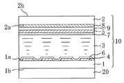
図1は、実施形態1の液晶表示素子を模式的に示す断面図である。図1を参照しながら、本実施形態の液晶表示素子を説明する。本実施形態の液晶表示素子は、単純マトリクス型の液晶表示素子であり、互いに対向する第1基板1および第2基板2と、第1基板1および第2基板2の間隙に介在する液晶層3と、第2基板2に形成された温度調節機能体を有する。第1基板1には、ストライプ状に複数の列電極4が設けられている。第2基板2には、列電極4と直交する複数の行電極5が設けられている。列電極4および行電極5は、いずれも表示用電極であり、ITO膜などの透明導電膜から形成され得る。列電極4および行電極5上には、ポリイミドからなる液晶配向膜6,7がそれぞれ設けられている。
【0053】
図2は、本実施形態の液晶表示素子における温度調整機構のシステム構成図である。温度調節機能体は、第1基板1および第2基板2にそれぞれ形成されていてもよく、また第2基板2に代えて第1基板1にのみ形成されていてもよい。温度調節機能体は、透光性を有する温度印加部8と、この温度印加部8に接続された温度制御部(不図示)を有する。本実施形態では、温度印加部8は、第2基板2の液晶層3側の面2aに形成されているが、第2基板2の外側の面2bに形成されていてもよく、第2基板2の両面2a,2bに形成されていてもよい。また、第2基板2に形成された温度印加部8とともに、あるいはこれに代えて、第1基板1の液晶層3側の面1aおよび/または外側面1bに、温度印加部8が形成されていてもよい。
【0054】
透光性の温度印加部8は、例えばITO(Indium Tin Oxide)、SnO2、ZnO、IZO(Indium Zinc Oxide )、GZO(Gallium Zinc Oxide)などの導電性の金属酸化物薄膜から形成することができる。これら金属酸化物薄膜は、EB(電子ビーム)蒸着法、スパッタ成膜法やゾルゲル法等の公知の手法で形成することができる。これらの金属酸化物薄膜に所定の通電信号を入力すると、薄膜に電流が流れて、薄膜の抵抗値に応じたジュール熱が発生するので、液晶表示素子を加温することが可能となる。本発明において「透光性」とは、波長400 〜800 nmの可視領域において、光線が40%以上透過できることを意味する。可視領域での光線透過率が40%未満の場合には、入射光線の大部分が遮蔽されるので、液晶パネルを透過する明るさが十分得られず、表示品位が大きく低下する。
【0055】
均一な液晶表示を実現させるには、少なくとも一方基板の少なくとも一方面の全面もしくは画素領域に、均一にパターニングした、ヒータ電極膜としての温度印加部8を形成することが望ましい。これにより、液晶パネルへの加温が偏在しないように調整することができる。温度印加部8のパターンとしては、例えば特開平5−173153号公報に開示されたパターンを採用することができる。
【0056】
第2基板2の内側(液晶層3側)の表示用電極(行電極5)下に温度印加部8を形成する場合には、半導体プロセスなどで利用される透明層間絶縁膜や有機系および有機−無機ハイブリッド系透明絶縁コート膜などの透明絶縁膜9を介して、表示用電極薄膜を積層形成することが望ましい。これにより、上下導電膜間のリークを防ぐことができる。
【0057】
なお、より簡便な透光性温度印加部として、表示用電極を利用しても良い。例えば、第2基板2の表示用電極(行電極5)の抵抗値や膜厚を設計して、表示用電極を加熱電源に接続してもよい。これにより、表示用電極は、温度印加部としての機能を併有することができる。
【0058】
さらに、透光性の温度印加部8としては、上記のような透明導電膜を用いた内部ヒータだけでなく、外部ヒータを用いることもできる。例えば、赤外線ヒータなどの外部ヒーターユニットを液晶パネルに接して配置することも可能である。赤外線ヒータは、例えばハロゲンヒーターランプやタングステンランプなどの赤外線/遠赤外線放射ランプ、セラミックヒータなどの赤外線輻射およびその制御・調節機能を有する構造体を包含する。また、液晶パネルにおいて、特に可視の近赤外域での入射光を調節するために、光学フィルタと組み合わせて使用することは、液晶パネルの色再現性を調節する際には有効である。その他、レーザ光を利用した熱源ヒータやホットプレートを利用した外部ヒータなども適用することが可能である。これらの各種温度印加部は組み合わせて導入することも可能である。
【0059】
温度印加部8に接続された温度制御部としては、ITO膜やその他電極膜の電気抵抗値の温度依存性などを利用した検出系による温度制御部が適用できる。例えば、温度検出部を通電した電流値と温度との検量線を求め、この検量線に基づいて温度補償するように外部信号をPID(Proportional Integral Differential)制御あるいはファジー制御などの手法で信号制御することが好ましい。温度検出部は、例えば所定の抵抗値を有するITO膜などの電極から形成される。
【0060】
温度調節機能体として、ペルチェ素子を組み込んでパネル温度を調節することも可能である。ペルチェ素子とは、P型・N型半導体接合などの異種接合界面を有する素子に電流を流した場合のペルチェ効果を利用した、熱電・冷却作用を有するモジュールである。電流の向きを変えることで、加熱作用と冷却作用が切り替わるという特徴を持つ。したがって、ペルチェ素子についても、電流制御部と組み合わせて温度調節機能体として適用することが有効である。
【0061】
以上のような構成の温度調節機能体を具備した液晶表示素子では、液晶パネル温度を容易にかつ均一に制御することが可能であり、液晶の表示モードや液晶組成物の種類に拘らず高速応答化を実現させることが可能となる。
【0062】
本発明の液晶表示素子は、好適なパネル温度T(℃)として、液晶層を構成する液晶組成物の液晶相−等方性相転移温度TNI(℃)を用いて、T1≦TNI−T≦T2(℃)(但し、T1=15,T2=65)の範囲に設定される。言い換えれば、液晶表示素子のパネル温度T(℃)が、TNI−65以上であり、かつTNI−15以下となるように温度制御される。TNI−Tが設定範囲下限値T1=15℃より低い場合には、液晶層を構成する液晶組成物の最適な温度条件よりもパネル温度が低すぎるので、例えば、回転粘性が大きくなりすぎる。したがって、表示に十分な応答速度が得られずに、動画表示のフレーム周期で残像が顕著に認められる。一方、TNI−Tが設定範囲上限値T2=65℃よりも高い場合には、液晶層を構成する液晶組成物の異方性の指標である秩序度S(オーダーパラメータ)が急激に低下する。したがって、液晶性が乏しくなり、光学的にもまた電気的にも異方性が小さくなるので、電界制御時の輝度やコントラスト低下、さらに閾値特性の劣化等の表示特性上の問題が発生する。中間調の応答も含めて1フレーム周期内(1/60秒内)に液晶応答を高速化するために、20≦TNI−T≦60の温度設定範囲がより好ましい。
【0063】
液晶パネルの温度管理は、上記の温度検出部などの検出系による管理に限定されない。例えば、液晶組成物の種類等が一義的に決定した場合には、液晶組成物の回転粘性γ1値と応答速度の温度依存性との検量線などに基づいて、温度を検出することも可能である。
【0064】
(高速応答液晶)
本実施形態の液晶表示素子に適用可能な高速応答液晶の表示モードとしては、旋光モードのTN(ねじれネマチィク)型、複屈折モードのECB(Electrically Controlled Birefringence )型、OCB(Optically Compensated Birefringence )型、HAN(Hybrid Aligned Nematic)型やSTN(Super Twisted Nematic )型などが挙げられる。また、本実施形態の液晶表示素子の表示形態としては、透過型液晶だけでなく、反射板等を組み合わせることで反射型液晶や反射透過両用型液晶にも応用可能である。
【0065】
本実施形態の液晶表示素子は、液晶層3を構成する液晶組成物の回転粘性γ1値が小さい。回転粘性の小さな液晶組成物は、一般に液晶の光学的、電気的異方性の小さい材料が多いので、表示品位と高速応答性を両立するために、液晶モードに合わせた材料の選択が極めて重要となる。
【0066】
本実施形態の液晶表示素子では、液晶組成物の液晶相−等方性相転移温度TNI(℃)を基準とした温度制限値での回転粘性γ1値を所定範囲内に限定している。具体的には、規定温度Ta=TNI−(T2−T1)/2(℃)(但し、T1=15,T2=65)、すなわちTNI−25(℃)の温度下においてγ1値を200mPa・s以下に限定している。規定温度Taが、このγ1値(200mPa・s)よりも大きな値の場合には、応答速度改善の効果が十分に見込むことができず、画像表示時においてシャドーイング(尾引き)残像が顕著となる。
【0067】
また、規定温度Taにおいて回転粘性γ1値が20mPa・s以上であることが好ましい。回転粘性γ1値が20mPa・sより小さい場合には、液晶材料の光学的な異方性を十分に保つことが困難になる。加えて、液晶材料の異方性が急激に低下することに起因して、温度やその他の動作環境の変化に対応する光学特性がシフトして、輝度やコントラストが大きく低下する。したがって、画像の表示品位が劣化して実用に耐えなくなるおそれがある。
【0068】
画像表示特性とパネル応答性改善の効果を考慮した場合の回転粘性γ1値のより好ましい範囲は、規定温度Taにおいて40mPa・s以上190mPa・s以下の範囲である。一般には、粘性係数が小さいほど高速応答性が実現しやすい。しかし、光学特性の観点では、粘性係数が大きいほど光学的な異方性も大きくなるので、パネルの輝度やコントラストを比較的大きく保ちやすくなる。
【0069】
液晶組成物の回転粘性γ1値は、例えばJpn.J.Appl.Phys.,33,L119(1994) や第23回液晶討論会予稿集212 頁(1997東京)などを参考にして、液晶パネルの過渡電流測定法から簡便に求めることができる。言い換えれば、液晶パネルの環境温度を変化させて、過渡電流測定法により回転粘性γ1値を評価することで、回転粘性γ1値の温度依存性を簡便に求めることができる。
【0070】
(実施形態2:アクティブマトリクス透過型液晶表示素子)
図3は、実施形態2の液晶表示素子を模式的に示す斜視図である。図3を参照しながら、本実施形態の液晶表示素子を説明する。なお、図3においては、図1に示す液晶表示素子の構成要素と実質的に同じ機能を有する構成要素を同じ参照符号で示し、その説明を省略する。
【0071】
本実施形態の液晶表示素子は、TFT(Thin Film Transistor)基板1と、TFT基板1に対向配置された対向基板2と、これら基板1,2間に配設されたTN液晶層3を有する。TFT基板1は、それぞれが行方向に延びる複数のゲートバスライン11と、ゲートバスライン11に対して直交して延びる複数のソースバスライン12と、ゲートバスライン11およびソースバスライン12の交差部近傍に設けられたTFT素子13と、TFT素子13を介してソースバスライン12に接続され、マトリクス状に配置された画素電極14を有する。TFT基板1の画素電極14上には、液晶配向膜(不図示)が設けられている。
【0072】
対向基板2には、実施形態1の第2基板2と同様に、透光性を有する温度印加部8、透明絶縁膜9、対向電極(共通電極)5および液晶配向膜7が順次積層されている。
【0073】
TFT基板1および対向基板2の各外側面には、それぞれ偏光板21,22が設けられている。本実施形態の液晶表示素子では、両偏光板21,22の偏光軸が互いに直交するように配置されている。
【0074】
TFT素子13は、ゲートバスライン11から与えられる走査信号によってスイッチング制御される。走査信号によってON状態とされたTFT素子13に接続されている画素電極14に信号電圧が印加される。信号電圧が印加された画素電極14と対向電極5との間の電位差によって、液晶層3中の液晶分子の配向状態が変化する。TFT基板1の外側から入射したバックライト光が液晶層3中を透過するとき、画素領域毎に光透過率が変調される。これにより、バックライト光を利用した透過表示が行われる。
【0075】
温度印加部8は、温度制御部(不図示)および温度検出部(不図示)に接続されている(図2参照)。温度検出部により液晶パネルの温度T(℃)がTNI−65未満であるか、あるいはTNI−15より高いと検出されると、温度制御部から温度印加部8に温度制御信号が入力される。これにより、温度印加部8が加熱または冷却されて、液晶パネル内の液晶層3が加熱または冷却される。
【0076】
本実施形態では、液晶パネルの対向基板2に温度調節機能体が形成されているが、これに限定されない。液晶パネルのTFT基板1にのみ温度調節機能体が形成されていても良く、あるいは両基板1,2にそれぞれ温度調節機能体が形成されていても良い。
【0077】
なお、本実施形態では、アクティブ駆動素子としてTFTを用いた場合について説明したが、これに限定されていない。例えば、MIM(Metal Insulator Metal)、BTB(バックツーバックダイオード)、ダイオードリング、バリスタまたはプラズマスイッチング等を用いることができる。
【0078】
本実施形態の液晶表示素子は、アクティブマトリクス型電気書き込み方式により情報の書き込みが行われる。しかし、本発明の液晶表示素子は、実施形態1の液晶表示素子のように単純マトリクス型電気書き込み方式でも良い。また、光書き込み方式、熱(レーザ)書き込み方式の液晶表示素子であっても良い。
【0079】
(実施形態3:投射型液晶表示装置)
実施形態1および2の液晶表示素子は、投射型液晶表示装置(プロジェクタ)の全般に適用可能である。投射型液晶表示装置は、液晶ライトバルブの背面を光源光で照射し、その透過光を投影レンズにて投影する構造を有している。実施形態3では、赤,緑,青のそれぞれ専用のライトバルブを配置した三板方式の投射型液晶表示装置について説明する。
【0080】
図4は、本実施形態の投射型液晶表示装置を示す概略図である。投射型液晶表示素子1000は、ランプ光源120を含む照明光学系100と、ランプ光源120からの光束(白色光束)を赤,緑,青の3原色の色光束に分離する色分離光学系200と、反射ミラー206を含むリレー光学系220と、赤,緑,青の3原色の光路に対応して配置された3つの液晶ライトバルブ300R,300G,300Bと、クロスダイクロイックプリズム522を含む色合成光学系520と、投影レンズ542を含む投影光学系540を備えている。
【0081】
照明光学系100から出射された光(白色光束)は、ダイクロイックミラー232を含む色分離光学系200によって、赤(R),緑(G),青(B)の3原色の色光束に分離される。色分離光学系200によって分離された色光束のそれぞれは、色光束のそれぞれに対応して液晶ライトバルブ300R,300G,300Bに入射する。液晶ライトバルブ300R,300G,300Bは、実施形態1または実施形態2に示した本発明による液晶表示素子である。各色光束は、液晶ライトバルブ300R,300G,300Bによって、画像情報に応じて変調される。変調された各色光束は、色合成光学系520のクロスダイクロイックプリズム522によって合成される。その後、投影レンズ542を含む投影光学系540によってスクリーン500上に投影されて、カラー画像が投影表示される。
【0082】
投射型液晶表示装置では、ランプ光源からの光を液晶ライトバルブに入射するので、液晶ライトバルブに局所的に熱がこもる。また、液晶パネル内での温度不均一に起因して、液晶表示ムラや応答速度のばらつき等が発生する。したがって、表示のちらつきなどの現象が見られるという課題がある。液晶ライトバルブへの温度調節機能の付加は、高速応答化の点に加えて、液晶表示特性を均一にするという観点からも効果が大きい。本発明の液晶表示素子は、パネル温度T(℃)が所定範囲に温度制御されているので、液晶ライトバルブとして好適に用いることができる。
【0083】
なお、本実施形態では、3つの液晶ライトバルブ300R,300G,300Bがいずれも、実施形態1または実施形態2に示した液晶表示素子であるが、3つの液晶ライトバルブのうち少なくとも1つの液晶ライトバルブが本発明の液晶表示素子であれば良い。例えば、青(B)に対応する液晶ライトバルブ300Bは、高い照射エネルギーを受けて、シール近傍で微小気泡が発生し易いので、青の液晶ライトバルブ300Bにのみ、本発明の液晶表示素子を適用しても良い。
【0084】
本実施形態では、色分離光学系200が、白色光束を赤,緑,青の色光束に分離する場合について説明したが、白色光束をシアン,マゼンタ,イエローの色光束に分離する色分離光学系を用いても良い。また、照明光学系100から出射された光を互いに異なる4色以上の色光束に分離する色分離光学系を用いても良い。
【0085】
本実施形態では、クロスダイクロイックプリズム522とダイクロイックミラー232を用いる三板式(3つの液晶ライトバルブを用いる方式)について説明した。しかし、クロスダイクロイックプリズムを用いずに、ダイクロイックミラーによって各色光束を合成する三板式に適用することもできる。また、本発明の投射型液晶表示装置は、複数の液晶表示素子を用いるが、本発明の液晶表示素子を単板式の投射型液晶表示装置に適用することもできる。例えば、赤(R),緑(G),青(B)の三原色のマイクロカラーフィルタを重ね合わせた1つのカラー液晶素子を用いる方式、1つの白黒型液晶素子と三原色のダイクロイックミラーとマイクロレンズアレイを用いる方式などが挙げられる。
【0086】
本実施形態の投射型液晶表示装置は、スクリーンの手前から投写するフロント投写方式であるが、反射ミラーを用いてスクリーンの背面から投写するリア投写方式に本発明の投射型液晶表示装置を適用しても良い。
【0087】
(実施形態4:画像シフト素子)
図5は、本実施形態の画像シフト素子を模式的に示す断面図である。本実施形態の画像シフト素子は、光の入射側に配置された液晶素子10と、光の出射側に配置された複屈折素子20を備える。なお、画像シフト素子は、液晶素子10と複屈折素子20とからなる組を少なくとも1組備えていれば良く、液晶素子10と複屈折素子20を2組以上備えていても良い。
【0088】
液晶素子10は、実施形態1の液晶表示素子と同様の構造を有する単純マトリクス型の液晶素子であり、実施形態1における液晶表示素子の各構成要素の説明をもって、本実施形態の液晶素子10の各構成要素の説明に代える。なお、図5において、実施形態1の液晶表示素子の構成要素と実質的に同じ機能を有する構成要素を共通の参照符号で示す。液晶素子10のモードとしては、周知のモードを適用することができる。例えば、TN(Twisted Nematic )、OCB(Optically Compensated Birefringence )、FLC(Ferroelectric Liquid Crystal)などである。
【0089】
複屈折素子20は、入射してきた直線偏光の偏光方向に応じて、光線をシフトさせる機能を有する。複屈折素子20は、複屈折性を有する、厚さtの一軸結晶などから構成される。例えば、水晶、ニオブ酸リチウム、方解石、雲母、ルチル(TiO2)、チリ硝石(NaNO3)などの材料が適用可能である。
【0090】
図6は、画像シフト素子の動作を説明する図である。図5および図6を参照しながら、本実施形態の画像シフト素子の動作について説明する。液晶素子10は、光が入射する第1の光入射面2bと、光が出射する第2の面(光出射面)1bを有し、印加電圧のON/OFFに応じて光の偏光状態を変化させることができる。言い換えれば、液晶素子10は、入射光の偏光軸を回転させずに、そのまま透過させる状態と、偏光軸を約90°回転させる状態との間でスイッチング動作を行う。なお、本願明細書での「偏光方向」とは、光の伝搬方向に垂直な方向であり、かつ電場ベクトルの振動面に平行な方向を意味する。
【0091】
液晶素子10によるスイッチング動作は、液晶層3に印加する電圧によって制御される。例えば、図6において、紙面に垂直な偏光成分の光が液晶素子10の左方から第1の面2bに入射した場合を想定する。液晶素子10が電圧無印加状態(例えば0ボルト)のときには、偏光軸が略90°回転した状態の偏光が液晶素子10の第2の面1bから出射される。この出射光の偏光軸は、紙面に平行となる。
【0092】
一方、液晶素子10が電圧印加状態(例えば5ボルト)のときには、偏光軸が回転しない状態の偏光が液晶素子10の第2の面1bから出射される。この出射光の偏光軸は、紙面に垂直なままである。
【0093】
液晶素子10の電圧印加がOFFのとき、複屈折素子20を透過した光は異常光としてシフトする。一方、液晶素子10の電圧印加がONのときには、複屈折素子20を透過した光(常光)はシフトしない。このシフト量は、複屈折素子20の厚さtによって調節することができる。ヘッド・マウント・ディスプレイ(HMD)のように、表示装置の総重量を小さくする必要がある場合、屈折率異方性(Δn)が相対的に大きなニオブ酸リチウムやルチルを用いることが好ましい。Δnが大きい材料であれば、所望の画像シフト量を得るために必要な複屈折素子20の厚さtを薄くできるので、小型化および軽量化に適している。
【0094】
本実施形態の画像シフト素子は、実施形態1の液晶表示素子と同様に、温度調整機能体を有する。温度調整機能体は、第1基板1および第2基板2にそれぞれ形成されていてもよく、また第2基板2に代えて第1基板1にのみ形成されていてもよい。温度調節機能体は、透光性を有する温度印加部8と、この温度印加部8に接続された温度制御部(不図示)を有する。本実施形態では、温度印加部8は、第2基板2の液晶層3側の面2aに形成されているが、第2基板2の外側の面2bに形成されていてもよく、第2基板2の両面2a,2bに形成されていてもよい。また、温度印加部8は、第2基板2に形成された温度印加部8とともに、あるいはこれに代えて、第1基板1の液晶層3側の面1aに形成されていても良く、第1基板1の外側面1bと複屈折素子20との間に形成されていても良い。さらに、複屈折素子20の外側面に温度印加部8が形成されていてもよい。
【0095】
本実施形態の画像シフト素子は、液晶素子10の温度を最適値に均一制御する温度調節機能体を備えているので、液晶の応答性が改善される。これにより、液晶素子10による画像シフト動作が改善されるので、表示品位が安定化する。
【0096】
本実施形態では、単純マトリクス型の液晶素子を用いた場合について説明したが、実施形態2で説明したアクティブマトリクス型液晶表示素子を液晶素子10として用いても良い。
【0097】
(実施形態5:画像表示装置)
本発明の液晶表示素子や画像シフト素子は、画像シフト技術を利用した画像表示装置に適用することができる。これにより、従来の画像表示装置で課題となっていた素子の応答性が大きく改善される。
【0098】
図7は、本実施形態の画像表示装置の構成を示す概略図である。本実施形態の画像表示装置は、光源220、光源220からの光を変調する透過型液晶表示素子15、画像シフト素子16および観察光学系17を備える。液晶表示素子15として、実施形態1または2で説明した液晶表示素子を用いることができ、画像シフト素子16として、実施形態4で説明した画像シフト素子を用いることができる。
【0099】
光源220は、液晶表示素子15を照明するバックライトや投射光源である。液晶表示素子15は、LCD(液晶表示素子)駆動回路18から駆動信号および映像信号を受け取り、映像信号に応じた画像情報を表示する。液晶表示素子15は、温度印加部8と温度制御部19とで構成された温度調節機能体によって、液晶層の温度が調整される。観察光学系17は、液晶表示素子15で表示された画像を光学的に拡大するための光学系である。観察者は、画像シフト素子16および観察光学系17を介して、液晶表示素子15で表示された画像を観察することができる。
【0100】
画像シフト素子16の動作は、画像シフト素子用の駆動回路21で制御される。具体的には、駆動回路21は、LCD駆動回路18から映像信号を受けて、液晶表示素子15の映像表示に同期した駆動信号を画像シフト素子16に供給する。これにより、画像シフト素子16は、液晶表示素子15に表示された画像を表示フレーム毎に光学的にシフトさせることができる。画像シフト素子16は、液晶表示素子15と同様に、温度印加部8と温度制御部19とで構成された温度調節機能体によって、液晶層の温度を設計値のレベルに均一に制御することができる。本実施形態の温度制御部19は、LCD駆動回路18からの制御信号を受けずに、言い換えればLCD駆動回路18から独立して、液晶表示素子15および画像シフト素子16の各温度印加部8を温度制御する。
【0101】
本実施形態の画像表示装置によれば、液晶表示素子15および画像シフト素子16の各液晶の応答性が改善されるので、表示品位が安定化する。なお、本実施形態では、液晶表示素子15および画像シフト素子16がともに温度制御されるが、液晶表示素子15のみ、または画像シフト素子16のみが温度制御されても良い。液晶表示素子15または画像シフト素子16のいずれか一方が温度制御されることによって、画質の改善が期待できる。
【0102】
また、本実施形態では、光源220からの光を変調する液晶表示素子15を用いているが、自発光型の表示素子を用いても良い。例えば、有機エレクトロルミネッセンス(EL)表示素子、無機EL表示素子、プラズマディスプレイパネル(PDP)などを用いても良い。
【0103】
(実施形態6:投射型画像表示装置)
本発明の画像表示装置は、図7に示す直視型の構成だけでなく、投射型表示装置にも応用できる。本実施形態の投射型画像表示装置は、ダイクロイックミラーとマイクロレンズアレイを用いた投射型液晶表示装置である。図8〜図10を参照しながら、本実施形態の投射型液晶表示装置を説明する。
【0104】
図8は、本実施形態の投射型液晶表示装置2000を示す概略図である。本実施形態の投射型液晶表示装置2000は、ランプ光源120と、ランプ光源120から出射した光束(白色光束)を略平行化させて反射させる放物面鏡600と、放物面鏡600からの光を変調させる液晶表示素子601と、液晶表示素子601を透過して変調された光を周期的に光学シフトさせる画像シフト素子606を備える。
【0105】
また、本実施形態の投射型液晶表示装置2000は、放物面鏡600からの光を液晶表示素子601に均一に照射するためのフライアイレンズ602と、フライアイレンズ602の出射側に配置され、液晶表示素子601に入射する照明光の平行度を規制するアパーチャ603と、アパーチャ603を通過した光を集光させるコンデンサレンズ604と、コンデンサレンズ604により集光した光をRGBの各光に分離するダイクロイックミラー605R,605G,605Bと、R, G, Bの3画素毎に1つの割合でマイクロレンズが配置されたマイクロレンズアレイ608と、画像シフト素子606により光学シフトされた光をスクリーン500上に投射するための投射レンズ607をさらに備える。
【0106】
本実施形態の投射型液晶表示装置2000の動作を説明する。光源120から出射した光束(白色光束)は、放物面鏡600で反射され、略平行化された後、フライアイレンズ602、アパーチャ603およびコンデンサレンズ604を経て、ダイクロイックミラー605R,605G,605Bに導かれる。ダイクロイックミラー605R,605G,605Bにより色分離された光は、色毎に異なる角度で液晶表示素子601に入射する。液晶表示素子601を透過して変調された光は、画像シフト素子606で周期的に光学シフトされた後、投射レンズ607を経て、スクリーン500上で画像を形成する。
【0107】
図9は、液晶表示素子601にR, G, Bの各光が入射する様子を示す概略図である。液晶表示素子606の入射光側には、マイクロレンズアレイ608が形成されたマイクロレンズ基板が配置されている。各マイクロレンズは、それぞれ異なる角度で入射したR, G, B光を対応する画素に入射させる。各画素の光透過率はそれぞれ独立して変調されるので、R, G, B光はそれぞれ独立して変調される。
【0108】
図10は、本実施形態で用いる液晶表示素子601および画像シフト素子606の構成例を示す概略図である。液晶表示素子601は、光入射側(ランプ光源120側)に温度印加部8を有する。液晶表示素子601は、実施形態1または2で説明した液晶表示素子と同様である。したがって、液晶表示素子601を構成する各構成要素の説明を省略する。
【0109】
画像シフト素子606は、2組の画像シフト素子から構成され、各組の画像シフト素子は、液晶素子と複屈折素子を備える。各組の画像シフト素子は、それぞれ温度印加部(不図示)を有する。画像シフト素子606は、光入射側から順に配置された第1の液晶素子30a、第1の複屈折素子31a、第2の液晶素子30bおよび第2の複屈折素子31bを有する。各構成部材は、市販の熱硬化型透明樹脂32などで接合される。液晶素子30a,30bおよび複屈折素子31a,31bは、実施形態4で説明した画像シフト素子の液晶素子10および複屈折素子20と同様である。したがって、液晶素子30a,30bおよび複屈折素子31a,31bを構成する各構成要素の説明を省略する。
【0110】
液晶表示素子601および液晶素子30a,30bは、それぞれ温度調整機能体を有する。温度調整機能体は、透明な温度印加部と、この温度印加部に接続されたヒータ駆動制御回路(温度制御部)を有する。温度印加部は、ヒータ駆動制御回路によって制御される。
【0111】
本実施形態のヒータ駆動制御回路(温度制御部)は、液晶表示素子601に画像信号を送る画像信号制御回路により制御される。画像信号制御回路による制御は、一サブフィールド期間内に、各画素へ送られる画像信号の総和の平均値(以下、平均レベル信号という)をヒータ駆動制御回路(温度制御部)へ送ることにより行われる。平均レベル信号によりヒータ駆動制御回路(温度制御部)を制御する理由について簡単に説明する。液晶表示素子601および液晶素子30a,30bでは、電圧ON−OFF時の応答速度、言い換えれば立ち上がり応答時間(τon)と立ち下がり応答時間(τoff)に大きな差が生じることがある。τonとτoffとで応答時間がずれると、画像の二重像が発生し、さらに二重像に起因したフリッカが発生するので、表示不良を引き起こす。この応答時間のずれは、液晶層の温度と密接な関係がある。一方、液晶表示素子601に送られる画像信号は、画素ごとにレベルが異なるので、液晶層の温度はパネル面内でばらつきが生じる。そこで、パネル面内での液晶温度のばらつきを抑えるために、ヒータ駆動用の信号を平均レベル信号で制御(補正)する。言い換えれば、パネル面内での温度制御のばらつきを抑える。これにより、液晶表示素子601および液晶素子30a,30bにおける応答時間のずれが低減される。
【0112】
本実施形態の投射型液晶表示装置2000は、液晶表示素子601および液晶素子30a,30bの温度を最適値に均一制御することができるので、液晶の応答速度が改善されて、画質が改善される。なお、液晶表示素子601および液晶素子30a,30bだけでなく、複屈折素子31a,31bも温度調節機能体を有していても良い。
【0113】
画像シフト素子606は、液晶表示素子601の表示画像の切り替えに同期して、液晶表示素子601から出た光をその光軸に対して垂直な方向に周期的にシフトさせる。複屈折素子31a,31bによる偏光状態を適切に切り替えることにより、3ポジションまたは4ポジションの画像シフトが行われる。これにより、見かけの表示画素数を3倍または4倍に向上させることができる。
【0114】
本実施形態の投射型液晶表示装置2000では、液晶表示素子601のサブフレーム期間に対応した画像信号に同期して、画像シフト素子606のシフト動作が行われる。具体的には、一方向(上下方向または左右方向)に1画素ずつ順次シフトさせる。これにより、液晶表示素子601の画像が重畳するので、高精細の画像がスクリーン500上に形成される。
【0115】
本実施形態の投射型液晶表示装置2000によれば、液晶パネルの温度設定を最適範囲に均一に制御することで、液晶表示素子601と画像シフト素子606の応答性が改善されて、表示品位が安定化する。なお、本実施形態では、液晶表示素子601および画像シフト素子606がともに温度制御されるが、液晶表示素子601のみ、または画像シフト素子606のみが温度制御されても良い。液晶表示素子601または画像シフト素子606のいずれか一方が温度制御されることによって、画質の改善が期待できる。
【0116】
次に、本発明の具体的な実施例および比較例を示す。本発明はこれらの実施例に限定されない。
【0117】
(実施例1〜6および比較例1〜5)
実施例1〜6および比較例1〜5で用いる液晶表示素子は、実施形態1で説明した、単純マトリクス透過型液晶表示素子である。まず、公知の技術により、第1基板としての透明ガラス基板上にITO膜を蒸着し、パターニング形成して、表示用電極を形成した。
【0118】
第2基板としての透明ガラス基板上に、温度印加部としてITO膜を全面に形成し、次いで温度検出用の金属電極端子を所定の位置に蒸着形成した。さらに、アクリル樹脂系の透明層間絶縁膜を成膜後、対向側の表示用ITO膜をパターニング形成した。第1および第2の両基板に液晶配向膜を形成した後、ラビング処理を施した。セルスペーサ(4μm)およびシール材を介して、両基板を貼り合わせて、液晶表示パネルを作製した。
【0119】
表1に記載された液晶材料を両基板間に真空注入し、封止して、TN型液晶表示素子を作製した。 作製した液晶パネルは、偏光顕微鏡を用いて所定の温度制御環境のもとで応答時間の評価(駆動電圧5V)を行った。 評価結果を表2にまとめて記載した。
【0120】
【表1】
【表2】
パネル応答時間は、駆動電圧5Vで評価し、中間調応答時間は電圧無印加状態から透過率80%を与える電圧V80に設定したときの緩和応答時間τで表す。なお、応答時間の目標値としては、60Hzのフィールド周波数での表示を目指した場合には、約17ms以下が必要となり、中間調応答についても20ms以下であることが望ましい。この評価試験では、液晶パネルのコントラスト値(CR比)は、表示品位の観点から、200 以上必要である。
【0123】
表1および表2の結果から、液晶パネル温度Tを本発明で規定する範囲内に制御することにより、高品位化と高速応答化を実現できることが判る。また、液晶材料の回転粘性γ1を本発明で規定する範囲内に限定することにより、応答時間がさらに改善されることが判る。
【0124】
実施例5,6および比較例5に示すように、規定温度Taにおいて液晶材料の回転粘性γ1値が200mPa・sを超える液晶材料Cを用いた場合には、液晶パネルの応答時間を目標値の範囲に設定することが難しくなる。しかし、実施例5および6に示すように、パネル温度T(℃)を制御することによって、応答速度の改善効果が確認された。
【0125】
次に、液晶材料A,BおよびCをそれぞれ用いたTN型液晶パネル(1〜3)において、設定パネル温度T(℃)が液晶パネルの表示品位に作用する影響について総合評価(パネルの応答時間、中間調応答時間およびコントラスト比)を行い、その評価結果を表3にまとめた。
【0126】
液晶パネルの応答時間については、駆動電圧5Vでの立ち上がりの応答時間(τr )および立ち下がりの応答時間(τd )で評価を行い、各応答時間(τr ,
τd )の目標値を17ms以下とした。中間調応答時間については、電圧無印加状態から透過率80%を与える電圧V80までの中間調応答時間τで評価を行い、20ms以下を目標値とした。液晶パネルのコントラスト比(CR比)については、直交ニコルに配置した偏光板間に液晶パネルを配置して、基準光源をバックライトとして評価し、200 以上を目標値とした。
【0127】
【表3】
表3では、全ての評価結果が目標値に達したとき“○”を表記し、最も動画表示時の表示品位のバランス(応答性とコントラスト)が良かった温度条件に“◎”を表記した。コントラスト比と応答時間(τr , τd )のみが目標値に達し、中間調応答時間が目標値に達していないとき“△”を表記し、それ以外の場合には表示品位が大きく損なわれるので“×”を表記した。
【0129】
表3に示すように、液晶材料の種類にかかわらず、液晶パネルの温度をTNI−65以上かつTNI−15以下、好ましくはTNI−30以上かつTNI−20以下の設定温度範囲に設計することで、液晶パネルの応答性とコントラスト比がともに目標値に到達すること、言い換えれば良好な表示品位を達成できることが確かめられた。
【0130】
本明細書で示したように、液晶パネルに温度調節機能を付与し、かつ最適な温度にパネルの温度を均一制御することで、極めて効果的に表示品位の改善が可能となる。
【0131】
(実施例7および比較例6)
実施例7および比較例6で用いる液晶表示素子は、実施形態2で説明した、アクティブマトリクス透過型液晶表示素子である。まず、公知の技術により、透明ガラス基板上に、複数の薄膜トランジスタ(TFT)素子および画素電極をマトリクス状に形成して、TFT基板を作製した。
【0132】
実施例7の対向基板は、透明ガラス基板上に、温度印加部としてのITO膜と温度検出用の金属電極端子をパターニング形成した後、透明絶縁保護膜を積層し、さらに、対向電極としてのITO膜を蒸着して、作製した。両基板に液晶配向膜を形成した後、ラビング処理を施した。セルスペーサ(4μm)およびシール材を介して、両基板を貼り合わせて、図2に示す液晶表示パネルを作製した。
【0133】
比較例6の対向基板は、温度印加部および金属電極端子がなく、透明ガラス基板上に対向電極(ITO膜)が形成された従来の対向基板である。この対向基板を用いて、実施例7と同様に、液晶表示パネルを作製した。
【0134】
実施例7および比較例6の各液晶表示パネルについて、表1に記載された液晶材料Bを両基板間に真空注入し、封止して、TN型液晶表示素子をそれぞれ作製した。 作製した液晶パネルを図4に示す投射型液晶プロジェクタのライトバルブとして適用し、投影評価を行った。
【0135】
実施例7では、液晶ライトバルブの設定温度Tを30℃(TNI−62℃)として評価した。液晶ライトバルブの温度設計を最適な条件で施した実施例7の場合には、動画表示においても残像現象がほとんど認められなかった。しかし、比較例6の従来のパネル設定では、動画表示時に少し残像現象が確認された。したがって、本発明の液晶表示素子をライトバルブとして用いることにより、効果的に液晶プロジェクタの応答速度が改善できることが確かめられた。
【0136】
(実施例8および実施例9)
実施例7と同様にして、TFT基板を作製した。対向基板は、透明ガラス基板上に、表示用ITO電極膜と温度検出用の金属電極端子をパターニング形成して作製した。実施例7と同様にして、液晶表示パネルを作製し、表1に記載された液晶材料Bを両基板間に真空注入し、封止して、TN型液晶表示素子を作製した。
【0137】
実施例8の液晶表示素子では、対向基板の外側(液晶層に対して反対側)に、遠赤外線を放射するハロゲンヒーターランプ(ウシオ電機社製)ユニットを温度調節機能体として設けた。また、実施例9の液晶表示素子では、対向基板の外側に、ペルチェ素子を組み込んだ温度調節ユニットを設けた。実施例8および実施例9の各ユニットをそれぞれの温度制御部に接続することによって、液晶パネルの外部に温度調節機能体が設けられた、温度調節機能付の液晶表示素子をそれぞれ作製した。
【0138】
実施例8および実施例9の液晶表示素子を、図4に示す投射型液晶プロジェクタのライトバルブとして適用し、投影評価を行った。液晶ライトバルブの設定温度Tを30℃(TNI−62℃)として評価した場合には、実施例8および実施例9の両者において同様の効果が確認できた。以上のように、液晶ライトバルブの外部に温度調節機能体を配置しても、最適なパネル温度に制御することによって、高品位化と高速応答化を実現できる。
【0139】
(実施例10および比較例7)
図8〜図10を参照しながら、実施形態6で説明した、投射型画像表示装置の実施例および比較例について説明する。なお、実施例10および比較例7で用いる液晶表示素子は、実施形態2で説明した、アクティブマトリクス透過型液晶表示素子である。
【0140】
実施例10の液晶表示素子601は、対向基板のマイクロレンズアレイ基板外側に、温度印加部8としてITO膜と、温度検出用の金属電極端子とがパターニング形成されている。一方、比較例7の対向基板は、温度調節機能を設けない、通常のマイクロレンズアレイ基板である。実施例10および比較例7では、表1の液晶材料Aを用いて、TN型液晶表示素子を作製した。
【0141】
実施例10の画像シフト素子は、温度調節用のITO透明ヒータ電極を施した液晶素子と複屈折素子を重ねて形成した。比較例7では、ヒータを施さない通常の液晶素子を用いた。3位置シフトの画像シフト素子を構成して、図8に示す投射型画像表示装置を作製した。
【0142】
このようにして作製した投射型画像表示装置を用いて投影評価を行った。評価は、液晶表示素子および画像シフト素子のサブフィールド駆動を同期させた映像で行った。
【0143】
実施例10では、液晶表示素子および画像シフト素子の各液晶パネルの設定温度Tを70℃(TNI−15℃)にして、映像を評価した。液晶ライトバルブの温度設計を最適な条件で施した実施例10の場合には、画像シフト処理で投影した動画表示においても、二重像、液晶の電圧応答性の遅延に伴うシフトずれや混色が認められなかった。
【0144】
しかし、比較例7の従来の液晶表示素子では、実施例10と同様の映像で評価したにもかかわらず、画像シフト時のタイミングずれにより二重像が発生し、これに起因したフリッカ発生が観察された。
【0145】
以上のことから、液晶パネルの温度を規定すること、さらに液晶組成物の回転粘性値を設計することは、液晶パネルの応答速度を改善させ、その結果として表示装置の画質改善に大きく寄与することが確かめられた。したがって、本発明によれば、画質が良好な画像表示装置が提供される。
【0146】
【発明の効果】
本発明の液晶表示素子によれば、輝度やコントラスト特性を損なうことなく、応答速度を効果的に改善して高速化を実現することが可能となる。多様な仕様や表示モードの液晶パネルに対しても、容易な手法で応答速度改善を達成できる。特に、液晶層を構成する液晶組成物の回転粘性γ1値についても、併せて最適値設定をすることで、より効果的に液晶表示の高品位化と高速応答化が実現可能である。それゆえ、本発明の液晶表示素子は、フルカラーで高い表示品位が求められる液晶表示装置、特に高い耐光性が要求される投射型液晶表示装置の液晶ライトバルブに好適である。
【0147】
本発明の画像シフト素子によれば、液晶表示素子の電圧レベルや液晶素子の電圧レベルに応じた応答時間を短縮化することができる。液晶素子の電圧応答の均一性が改善され、サブフィールド期間内での液晶応答性が向上する。したがって、画像シフト技術を応用した高品位でかつ高解像度の画像表示装置を提供することができる。
【図面の簡単な説明】
【図1】 実施形態1の液晶表示素子を模式的に示す断面図である。
【図2】 実施形態1の液晶表示素子における温度調整機構のシステム構成図である。
【図3】 実施形態2の液晶表示素子を模式的に示す斜視図である。
【図4】 実施形態3の投射型液晶表示装置を示す概略図である。
【図5】 実施形態4の画像シフト素子を模式的に示す断面図である。
【図6】 画像シフト素子の動作を説明する図である。
【図7】 実施形態5の画像表示装置の構成を示す概略図である。
【図8】 実施形態6の投射型液晶表示装置2000を示す概略図である。
【図9】 液晶表示素子601にR, G, Bの各光が入射する様子を示す概略図である。
【図10】 液晶表示素子601および画像シフト素子606の構成例を示す概略図である。
【符号の説明】
1 第1基板(TFT基板)
2 第2基板(対向基板)
3 液晶層
4 表示用電極(列電極)
5 表示用電極(行電極)
8 温度印加部(透明電極膜)
9 透明絶縁膜
15 液晶表示素子
16,606 画像シフト素子
10,30a,30b 液晶素子
20,31a,31b 複屈折素子
120 ランプ光源
200 色分離光学系
300R,300G,300B 液晶ライトバルブ(液晶表示素子)
520 色合成光学系
540 投影光学系
17 観察光学系
1000,2000 投射型液晶表示装置(プロジェクタ)[0001]
BACKGROUND OF THE INVENTION
The present invention relates to a liquid crystal display element and an image shift element. The liquid crystal display element and the image shift element of the present invention can be used in an image display apparatus, for example, a transmissive display apparatus such as a projector.
[0002]
[Prior art]
[Conventional technology for liquid crystal display devices]
[0003]
[Patent Document 1]
JP-A-2-55322
[0004]
[Patent Document 2]
JP-A-9-96824
[0005]
[Patent Document 3]
JP-A-8-71084
[0006]
[Patent Document 4]
JP 2001-83480 A
In recent years, the rapid development of high-speed response, high brightness, and high contrast of liquid crystal displays has rapidly progressed, and liquid crystal display devices and projection type liquid crystal display devices that can handle moving image display while ensuring display quality have been developed. It has been demanded.
[0007]
[Conventional Technology for Image Shift Elements]
In
[0008]
[Patent Document 5]
US Pat. No. 6,061,103
[0009]
[Patent Document 6]
JP-A-8-194207
By the way, as a driving method of the image display apparatus, interlace driving, non-interlace driving, or the like is widely adopted. Interlaced driving is a driving method in which odd or even rows are selected for each field, and one image is formed by odd and even fields, and the selection time of each field is normally 16.6 milliseconds (60 Hz). . On the other hand, non-interlaced driving is a driving method in which selection is performed sequentially regardless of odd-numbered rows and even-numbered rows, and the selection time of each field is similarly 16.6 milliseconds (60 Hz). Here, the field refers to a period of vertical synchronization of images, and in a liquid crystal display device, a scan period including blanking time corresponds to a field period.
[0010]
In the image display devices of
[0011]
However, when the conventional liquid crystal element is used, the response time becomes longer than the subfield selection period, or the rise response time (τon) And fall response time (τoff) May cause a difference in timing at the time of image shift. If the timing at the time of image shift is shifted, a double image is generated, and further flicker due to the double image is generated. Therefore, there is a problem that image quality deterioration is increased.
[0012]
As described above, in the image display device using wobbling, it is essential to improve the response characteristics of the liquid crystal elements constituting the image shift element, and the liquid crystal display elements for image display are also synchronized with the subfield period to be selected. Fast response is essential. That is, when a conventional liquid crystal element is used, further improvement in image quality is required.
[0013]
On the other hand, by using two or more combinations of liquid crystal elements and birefringent elements, an image shift element having a shift position of three positions or more can be obtained. In this image shift element, unlike the case where only one liquid crystal element is used, it is necessary to match the response speeds of the plurality of liquid crystal elements. In other words, if the response time is different for each liquid crystal element, the image shift timing varies and the image quality is significantly degraded. Therefore, the temperature of all the liquid crystal elements must be kept uniform.
[0014]
In the liquid crystal element, in consideration of the panel temperature and the temperature characteristics of the liquid crystal composition, a design capable of high-quality and high-speed response to various liquid crystal panel configurations and display modes is extremely important. Normally, the display quality related to the image quality such as brightness and contrast is lowered only by heating the liquid crystal panel. In addition, it is difficult to realize a high-quality and high-definition image display device only by pursuing high-speed responsiveness synchronized with the subfield period only for the liquid crystal elements constituting the image shift element. That is, it is important for the liquid crystal display element that modulates the light from the light source according to the signal to display the image information synchronized with the subfield period and to guide the image information to the image shift element. It is required to uniformly control the temperature of both the element and the image shift element.
[0015]
For the purpose of improving the response characteristics of the liquid crystal element,
[0016]
[Patent Document 7]
Japanese Patent Laid-Open No. 11-326877
[0017]
[Problems to be solved by the invention]
An object of the present invention is to provide a liquid crystal display device and a projection type liquid crystal display device in which the response speed of the panel is improved without deteriorating display quality related to image quality such as brightness and contrast. In the current liquid crystal display device, since the response characteristic in the halftone state is not sufficient, an afterimage phenomenon or the like accompanying the moving image display of the liquid crystal is recognized. Therefore, development of a liquid crystal panel corresponding to high-quality full-color moving image display is desired. Efforts such as application of a high-speed display mode, use of a driving method, improvement of liquid crystal materials, etc. have been attempted for high-speed response of liquid crystal display devices, but there is a problem that complicated panel design is required . Therefore, there is a demand for a simpler and faster technique.
[0018]
The present invention aims to realize a liquid crystal display device capable of high-quality and high-speed response to various liquid crystal panels and display modes by designing considering the temperature of the liquid crystal panel and the temperature characteristics of the liquid crystal composition. Yes.
[0019]
Another object of the present invention is to shorten the response time according to the voltage level of the liquid crystal display element and the voltage level of the liquid crystal element constituting the image shift element in the image shift element. Furthermore, by improving the uniformity of the voltage response of the liquid crystal element, the liquid crystal response within the subfield period is improved, and a high-definition and high-resolution image display device applying image shift technology is provided. Is another purpose.
[0020]
[Means for Solving the Problems]
In order to solve the above-described problem, in the present invention, the panel temperature of the liquid crystal display device is regulated to an optimum range in relation to the liquid crystal composition constituting the liquid crystal layer and the phase transition temperature. In addition, the above-described problem is solved by designing an optimum value of the rotational viscosity value of the liquid crystal composition depending on the temperature characteristics.
[0021]
Specifically, the liquid crystal display device is provided with a temperature adjustment function body, and the liquid crystal panel temperature is designed in an optimum temperature range, thereby achieving the object. Furthermore, considering that the temperature dependence of the physical properties of the liquid crystal composition constituting the liquid crystal layer changes, the rotational viscosity γ1By defining an optimum value for the value, the above-mentioned problem can be solved more effectively.
[0022]
In addition, the present invention discloses a technique for increasing the resolution by shifting the pixel information constituting the image of the display element in a time division manner and displaying the pixel information superimposed. In particular, a technique for preventing the occurrence of flicker, color mixing and blurring due to double images by improving the liquid crystal response synchronized with the subfield switching timing of the display element and the voltage responsiveness of the image shift element is disclosed. .
[0023]
Specifically, the purpose is achieved by providing a temperature adjustment function body in the display element and the image shift element, designing the liquid crystal panel temperature in the optimum temperature range, and improving the response speed. Furthermore, the rotational viscosity γ of the liquid crystal composition in the liquid crystal panel constituting the display element or the image shift element1By defining the value and the like, the above-described problem can be effectively solved.
[0024]
In general, the dynamic switching behavior of liquid crystal molecules responding to an electric field when nematic liquid crystal is used is approximately expressed by the following equation.
[0025]
τoff= Γ1d2/ Kπ2 (Formula 1)
τon= Τoff/ {(V2/ Vth2-1} (Formula 2)
Vth= Π (K / Δε)1/2 (Formula 3)
Where τoff; Response time when the voltage to the panel is turned off (fall time), τon; Response time (rise time) when voltage is applied to the panel, VthThreshold voltage, V: applied voltage, d: liquid crystal cell thickness, γ1The rotational viscosity of the liquid crystal composition, K the elastic constant of the liquid crystal, Δε the dielectric anisotropy of the liquid crystal.
[0026]
From these relational expressions, as a method of increasing the response speed of the liquid crystal display device, (1) designing the liquid crystal cell thickness to be small, (2) designing the applied voltage high when driving the liquid crystal, (3) For example, the optimum design of the physical property parameters of the liquid crystal material can be mentioned.
[0027]
However, the following problems exist for the above methods. (1) The reduction of the liquid crystal cell thickness not only reduces the allowable cell thickness range in the manufacturing aspect of the liquid crystal display device and decreases the yield, but also tends to cause a decrease in luminance in the display quality of the liquid crystal panel. Therefore, it is necessary to combine with high Δn liquid crystal, wavelength dispersion tends to be remarkable, and cell thickness reduction can be applied only within a limited range from the viewpoint of optical design.
[0028]
(2) By setting the applied voltage at the time of driving the liquid crystal large, it is possible to shorten the response time especially at the time of rising, but it cannot be easily applied because it increases the power consumption.
[0029]
(3) Among the optimization of liquid crystal material surface, rotational viscosity γ1Reducing τoffAnd τo nHowever, it is necessary to adjust the balance between Δε and Δn of the liquid crystal material. In addition, since each physical property value of the material shows temperature dependence, selection of the material is an extremely important item.
[0030]
In the present invention, by adjusting the panel temperature, the rotational viscosity γ of the liquid crystal composition constituting the liquid crystal layer is further increased.1By adjusting, the speed of the liquid crystal is increased. In particular, the rotational viscosity γ of the liquid crystal composition1By adjusting this optimization, it is possible to effectively improve the delay of the halftone response time of the liquid crystal display device.
[0031]
Rotational viscosity coefficient γ of liquid crystal material1Is also known to satisfy the following Andrade's equation, as with ordinary liquids.
[0032]
(Andrad equation) γ1= A exp (B / T) (Formula 4)
Where A and B are constants and T is an absolute temperature.
[0033]
From this relationship, the rotational viscosity γ1It can be seen that the temperature decreases exponentially with increasing temperature. It can also be seen that temperature adjustment is effective in improving the response speed of the liquid crystal display device. The physical properties of liquid crystal materials such as Δε and Δn also change so that the anisotropy decreases with increasing temperature, as well as the degree of order S. Therefore, a comprehensive design that takes into account the temperature dependence of various physical properties is necessary. It becomes. From the viewpoint of improving the response speed, it is considered most effective to design the liquid crystal panel by paying attention to the rotational viscosity after adjusting the optical and electrical anisotropy depending on the temperature.
[0034]
The liquid crystal display element of the present invention includes a first substrate and a second substrate facing each other, a liquid crystal layer interposed in a gap between the first substrate and the second substrate, and the first substrate and / or the second substrate. A liquid crystal display element having a formed temperature control function body, wherein a liquid crystal phase-isotropic phase transition temperature of a liquid crystal composition constituting the liquid crystal layer is expressed by TNI(° C.), the panel temperature T (° C.) of the liquid crystal display element is TNI-65 or more and TNI-15 or less, preferably TNI-30 or more and TNITemperature is controlled at -20 or less.
[0035]
Rotational viscosity γ of the liquid crystal composition1But TNIIt is preferably 200 mPa · s or less at a temperature of −25 (° C.). Further, the rotational viscosity γ of the liquid crystal composition1But TNIIt is preferably 20 mPa · s or more at a temperature of −25 (° C.).
[0036]
The temperature control function body includes a light-transmitting temperature application unit formed on at least one surface of the first substrate and the second substrate, and a temperature control unit connected to the temperature application unit.NoThe
[0037]
The temperature application part is formed of a transparent conductive film.Yes.The temperature application unit is patterned to correspond to a predetermined display area.Yes.In the present specification, the “display region” refers to a region in which pixels that are the minimum unit of display are arranged in a matrix. In the active matrix liquid crystal display device, the “pixel region” is defined by a pixel electrode and a counter electrode disposed to face the pixel electrode. In a simple matrix liquid crystal display device, a “pixel region” is defined by column electrodes provided in a stripe shape and row electrodes provided so as to be orthogonal to the column electrodes. Strictly speaking, in the configuration in which the black matrix is provided, the region corresponding to the opening of the black matrix corresponds to the pixel region among the regions to which the voltage is applied according to the state to be displayed. In the present specification, the “display area” may include an area provided with a black matrix.
[0038]
A display electrode may be formed on the temperature application unit via a transparent insulating layer. The temperature application unit may be an infrared heater. The temperature control function body may have a Peltier element.
[0039]
A projection display device according to a first aspect of the present invention includes a light source, a color separation optical system that separates a light beam from the light source into a plurality of different color light beams, and a plurality of light beams separated by the color separation optical system. A plurality of liquid crystal display elements arranged corresponding to each of the color light beams, a color combining optical system for combining the plurality of color light beams modulated by each of the plurality of liquid crystal display elements, and the color combining optical system A projection-type liquid crystal display device including a projection optical system that projects the plurality of color light beams synthesized by the at least one liquid crystal display element, wherein at least one liquid crystal display element is the liquid crystal display element of the present invention. .
[0040]
The image shift element of the present invention is an image having at least one combination of a liquid crystal element that modulates the polarization state of light and a birefringence element that shifts an optical path according to the polarization state of the light emitted from the liquid crystal element. A shift element, wherein the liquid crystal element includes a first substrate and a second substrate facing each other, a liquid crystal layer interposed in a gap between the first substrate and the second substrate, the first substrate and / or the first substrate. A liquid crystal phase-isotropic phase transition temperature of a liquid crystal composition having a temperature control function body formed on two substrates and constituting the liquid crystal layer is defined as TNI(° C.), the panel temperature T (° C.) of the liquid crystal element is TNI-65 or more and TNITemperature is controlled at -15 or less.
[0041]
Rotational viscosity γ of the liquid crystal composition1But TNIIt is preferably 200 mPa · s or less at a temperature of −25 (° C.). Further, the rotational viscosity γ of the liquid crystal composition1But TNIIt is preferably 20 mPa · s or more at a temperature of −25 (° C.).
[0042]
The temperature adjustment function body includes a light-transmitting temperature application unit formed on at least one surface of the first substrate and the second substrate, and a temperature control unit connected to the temperature application unit. May be.
[0043]
The temperature application part is formed of a transparent conductive film.Yes.The temperature application unit is patterned to correspond to a predetermined display area.Yes.
[0044]
A display electrode may be formed on the temperature application unit via a transparent insulating layer. The temperature application unit may be an infrared heater. The temperature control function body may have a Peltier element. The birefringent element may have a temperature adjustment function body.
[0045]
An image display device according to a first aspect of the present invention includes a light source, a liquid crystal display element of the present invention that modulates light from the light source, and a light emitting side of the liquid crystal display element, and is displayed on the liquid crystal display element. An image shift element that optically shifts the generated image for each display frame is provided.
[0046]
An image display device according to a second aspect of the present invention includes a display element and the image shift element of the present invention disposed on the light emission side of the display element. The display element may be the liquid crystal display element of the present invention. The image shift element may shift light emitted from the display element in synchronization with display on the display element.
[0047]
A projection-type liquid crystal display device according to a second aspect of the present invention includes a light source, the liquid crystal display element of the present invention that modulates light from the light source, and the light emission side of the liquid crystal display element. An image shift element that optically shifts the image displayed on each display frame, and a projection optical system that projects an image superimposed by the image shift element.
[0048]
A projection-type liquid crystal display device according to a third aspect of the present invention includes a light source, a liquid crystal display element that modulates light from the light source, and an image shift element of the present invention that is disposed on the light emission side of the liquid crystal display element. And a projection optical system for projecting the image superimposed by the image shift element. The liquid crystal display element may be the liquid crystal display element of the present invention.
[0049]
According to the liquid crystal display element and the projection display device of the present invention, by adjusting the temperature of the liquid crystal panel to the optimum temperature range, the response speed can be effectively improved without impairing the brightness and contrast characteristics, and the high speed can be achieved. Can be realized. In other words, by adjusting the temperature of the liquid crystal panel and setting it to the optimum temperature range, it is possible to achieve an improved response speed with a simple method even for liquid crystal panels of various specifications and display modes. In addition, the rotational viscosity γ of the liquid crystal composition constituting the liquid crystal layer1By defining the physical property value of the liquid crystal display, it is possible to achieve higher quality and faster response of the liquid crystal display more effectively.
[0050]
According to the image shift element of the present invention, by adjusting the temperature of the liquid crystal panel to an optimum temperature range, the liquid crystal response in the panel is not uneven, and high-speed response can be realized. By applying the image shift element of the present invention to an image display device such as a projection type liquid crystal display device, display quality can be improved.
[0051]
DETAILED DESCRIPTION OF THE INVENTION
Hereinafter, embodiments of the present invention will be described.
[0052]
(Embodiment 1: Simple matrix transmission type liquid crystal display element)
FIG. 1 is a cross-sectional view schematically showing the liquid crystal display element of the first embodiment. The liquid crystal display element of this embodiment will be described with reference to FIG. The liquid crystal display element of this embodiment is a simple matrix type liquid crystal display element, and the
[0053]
FIG. 2 is a system configuration diagram of a temperature adjustment mechanism in the liquid crystal display element of the present embodiment. The temperature control function body may be formed on each of the
[0054]
The translucent
[0055]
In order to realize a uniform liquid crystal display, it is desirable to form the
[0056]
When the
[0057]
A display electrode may be used as a simpler translucent temperature application unit. For example, the resistance value and film thickness of the display electrode (row electrode 5) of the
[0058]
Furthermore, as the translucent
[0059]
As the temperature control unit connected to the
[0060]
It is also possible to adjust the panel temperature by incorporating a Peltier element as the temperature adjustment function body. The Peltier element is a module having a thermoelectric / cooling action utilizing the Peltier effect when a current is passed through an element having a heterogeneous junction interface such as a P-type / N-type semiconductor junction. By changing the direction of the current, the heating and cooling functions are switched. Therefore, it is effective to apply the Peltier element as a temperature control function body in combination with the current control unit.
[0061]
The liquid crystal display device having the temperature control function body configured as described above can easily and uniformly control the temperature of the liquid crystal panel, and can respond quickly regardless of the display mode of the liquid crystal or the type of liquid crystal composition. Can be realized.
[0062]
The liquid crystal display element of the present invention has a liquid crystal phase-isotropic phase transition temperature T of the liquid crystal composition constituting the liquid crystal layer as a suitable panel temperature T (° C.).NI(° C), T1≦ TNI-T ≦ T2(℃) (However, T1= 15, T2= 65). In other words, the panel temperature T (° C.) of the liquid crystal display element is TNI-65 or more and TNIThe temperature is controlled to be -15 or less. TNI-T is the setting range lower limit T1When the temperature is lower than 15 ° C., the panel temperature is too low than the optimum temperature condition of the liquid crystal composition constituting the liquid crystal layer, and thus, for example, the rotational viscosity becomes too large. Therefore, a response speed sufficient for display cannot be obtained, and an afterimage is noticeable in the frame period of the moving image display. On the other hand, TNI-T is the setting range upper limit T2When the temperature is higher than 65 ° C., the degree of order S (order parameter), which is an index of anisotropy of the liquid crystal composition constituting the liquid crystal layer, rapidly decreases. Accordingly, the liquid crystal properties are poor, and the optical and electrical anisotropies are reduced, which causes problems in display characteristics such as luminance and contrast reduction during electric field control, and further deterioration in threshold characteristics. In order to speed up the liquid crystal response within one frame period (within 1/60 seconds) including halftone response, 20 ≦ TNIA temperature setting range of −T ≦ 60 is more preferable.
[0063]
The temperature management of the liquid crystal panel is not limited to the management by the detection system such as the temperature detection unit described above. For example, when the type of liquid crystal composition is uniquely determined, the rotational viscosity γ of the liquid crystal composition1It is also possible to detect the temperature based on a calibration curve between the value and the temperature dependence of the response speed.
[0064]
(High-speed response LCD)
As a display mode of the high-speed response liquid crystal applicable to the liquid crystal display element of the present embodiment, an optical rotation mode TN (twisted nematic) type, a birefringence mode ECB (Electrically Controlled Birefringence) type, an OCB (Optically Compensated Birefringence) type, Examples include a HAN (Hybrid Aligned Nematic) type and a STN (Super Twisted Nematic) type. Further, the display form of the liquid crystal display element of the present embodiment can be applied not only to the transmissive liquid crystal but also to the reflective liquid crystal and the reflective / transmissive liquid crystal by combining a reflector and the like.
[0065]
The liquid crystal display element of the present embodiment has a rotational viscosity γ of the liquid crystal composition constituting the liquid crystal layer 3.1The value is small. Liquid crystal compositions with small rotational viscosity generally have many materials with small optical and electrical anisotropy of liquid crystals. Therefore, selection of materials suitable for the liquid crystal mode is extremely important in order to achieve both display quality and high-speed response. It becomes.
[0066]
In the liquid crystal display element of this embodiment, the liquid crystal phase-isotropic phase transition temperature T of the liquid crystal composition.NIRotational viscosity γ with temperature limit value based on (℃)1The value is limited within a predetermined range. Specifically, the specified temperature Ta = TNI-(T2-T1) / 2 (° C) (however, T1= 15, T2= 65), ie TNIΓ at a temperature of −25 (° C.)1The value is limited to 200 mPa · s or less. The specified temperature Ta is γ1When the value is larger than the value (200 mPa · s), the effect of improving the response speed cannot be sufficiently expected, and shadowing (tailing) afterimage becomes remarkable at the time of image display.
[0067]
In addition, the rotational viscosity γ at the specified temperature Ta1The value is preferably 20 mPa · s or more. Rotational viscosity γ1When the value is smaller than 20 mPa · s, it becomes difficult to sufficiently maintain the optical anisotropy of the liquid crystal material. In addition, due to the sudden decrease in anisotropy of the liquid crystal material, optical characteristics corresponding to changes in temperature and other operating environments are shifted, and brightness and contrast are greatly reduced. Therefore, there is a possibility that the display quality of the image deteriorates and cannot be practically used.
[0068]
Rotational viscosity γ considering the effect of improving image display characteristics and panel response1A more preferable range of the value is a range of 40 mPa · s to 190 mPa · s at the specified temperature Ta. In general, the smaller the viscosity coefficient, the easier it is to realize high-speed response. However, from the viewpoint of optical characteristics, the greater the viscosity coefficient, the greater the optical anisotropy, so that the brightness and contrast of the panel can be kept relatively large.
[0069]
Rotational viscosity γ of liquid crystal composition1For example, Jpn.J.Appl.Phys.,33, L119 (1994) and the 23rd Liquid Crystal Symposium Proceedings, page 212 (1997 Tokyo), etc., can be easily obtained from the transient current measurement method of the liquid crystal panel. In other words, by changing the environmental temperature of the liquid crystal panel, the rotational viscosity γ1By evaluating the value, rotational viscosity γ1The temperature dependence of the value can be easily determined.
[0070]
(Embodiment 2: Active matrix transmission type liquid crystal display element)
FIG. 3 is a perspective view schematically showing the liquid crystal display element of the second embodiment. The liquid crystal display element of this embodiment will be described with reference to FIG. In FIG. 3, constituent elements having substantially the same functions as those of the liquid crystal display element shown in FIG. 1 are denoted by the same reference numerals, and description thereof is omitted.
[0071]
The liquid crystal display element of this embodiment includes a TFT (Thin Film Transistor)
[0072]
Similar to the
[0073]
Polarizing
[0074]
The
[0075]
The
[0076]
In this embodiment, the temperature control function body is formed on the
[0077]
In the present embodiment, the case where a TFT is used as the active drive element has been described. However, the present invention is not limited to this. For example, MIM (Metal Insulator Metal), BTB (back-to-back diode), diode ring, varistor, or plasma switching can be used.
[0078]
In the liquid crystal display element of this embodiment, information is written by an active matrix electric writing method. However, the liquid crystal display element of the present invention may be a simple matrix type electric writing method like the liquid crystal display element of the first embodiment. Further, a liquid crystal display element of an optical writing method or a thermal (laser) writing method may be used.
[0079]
(Embodiment 3: Projection type liquid crystal display device)
The liquid crystal display elements of
[0080]
FIG. 4 is a schematic view showing the projection type liquid crystal display device of the present embodiment. The projection-type liquid
[0081]
The light (white light beam) emitted from the illumination
[0082]
In the projection type liquid crystal display device, the light from the lamp light source is incident on the liquid crystal light bulb, and heat is locally accumulated in the liquid crystal light bulb. Further, due to temperature non-uniformity in the liquid crystal panel, liquid crystal display unevenness, response speed variation, and the like occur. Therefore, there is a problem that a phenomenon such as display flickering is observed. The addition of the temperature adjustment function to the liquid crystal light valve is highly effective from the viewpoint of uniform liquid crystal display characteristics in addition to the high speed response. The liquid crystal display element of the present invention can be suitably used as a liquid crystal light valve because the panel temperature T (° C.) is controlled within a predetermined range.
[0083]
In the present embodiment, the three liquid crystal
[0084]
In the present embodiment, the case where the color separation
[0085]
In the present embodiment, the three-plate type (method using three liquid crystal light valves) using the cross
[0086]
The projection type liquid crystal display device of the present embodiment is a front projection method that projects from the front of the screen, but the projection type liquid crystal display device of the present invention is applied to a rear projection method that projects from the back of the screen using a reflection mirror. May be.
[0087]
(Embodiment 4: Image shift element)
FIG. 5 is a cross-sectional view schematically showing the image shift element of the present embodiment. The image shift element of the present embodiment includes a
[0088]
The
[0089]
The
[0090]
FIG. 6 is a diagram for explaining the operation of the image shift element. The operation of the image shift element of this embodiment will be described with reference to FIGS. The
[0091]
The switching operation by the
[0092]
On the other hand, when the
[0093]
When the voltage application of the
[0094]
Similar to the liquid crystal display element of the first embodiment, the image shift element of the present embodiment has a temperature adjustment function body. The temperature adjustment function body may be formed on each of the
[0095]
Since the image shift element of this embodiment includes a temperature adjustment function body that uniformly controls the temperature of the
[0096]
In this embodiment, the case where a simple matrix liquid crystal element is used has been described. However, the active matrix liquid crystal display element described in
[0097]
(Embodiment 5: Image display device)
The liquid crystal display element and the image shift element of the present invention can be applied to an image display apparatus using an image shift technique. Thereby, the responsiveness of the element which has been a problem in the conventional image display device is greatly improved.
[0098]
FIG. 7 is a schematic diagram showing the configuration of the image display apparatus of the present embodiment. The image display apparatus of this embodiment includes a
[0099]
The
[0100]
The operation of the
[0101]
According to the image display device of the present embodiment, the responsiveness of each liquid crystal of the liquid crystal display element 15 and the
[0102]
In the present embodiment, the liquid crystal display element 15 that modulates light from the
[0103]
(Embodiment 6: Projection-type image display device)
The image display apparatus of the present invention can be applied not only to the direct view type configuration shown in FIG. 7 but also to a projection type display apparatus. The projection type image display device of this embodiment is a projection type liquid crystal display device using a dichroic mirror and a microlens array. The projection type liquid crystal display device of this embodiment will be described with reference to FIGS.
[0104]
FIG. 8 is a schematic diagram showing a projection type liquid
[0105]
Further, the projection type liquid
[0106]
The operation of the projection type liquid
[0107]
FIG. 9 is a schematic view showing a state in which each light of R, G, and B is incident on the liquid
[0108]
FIG. 10 is a schematic diagram illustrating a configuration example of the liquid
[0109]
The
[0110]
The liquid
[0111]
The heater drive control circuit (temperature control unit) of this embodiment is controlled by an image signal control circuit that sends an image signal to the liquid
[0112]
Since the projection type liquid
[0113]
The
[0114]
In the projection type liquid
[0115]
According to the projection type liquid
[0116]
Next, specific examples and comparative examples of the present invention will be shown. The present invention is not limited to these examples.
[0117]
(Examples 1-6 and Comparative Examples 1-5)
The liquid crystal display elements used in Examples 1 to 6 and Comparative Examples 1 to 5 are the simple matrix transmission type liquid crystal display elements described in the first embodiment. First, an ITO film was vapor-deposited on a transparent glass substrate as a first substrate by a known technique, and patterned to form a display electrode.
[0118]
On the transparent glass substrate as the second substrate, an ITO film was formed as a temperature application portion on the entire surface, and then a metal electrode terminal for temperature detection was formed by evaporation at a predetermined position. Further, after forming an acrylic resin-based transparent interlayer insulating film, an opposing display ITO film was formed by patterning. A liquid crystal alignment film was formed on both the first and second substrates and then rubbed. Both substrates were bonded together via a cell spacer (4 μm) and a sealing material to produce a liquid crystal display panel.
[0119]
A liquid crystal material described in Table 1 was vacuum-injected between both substrates and sealed to prepare a TN liquid crystal display element. The produced liquid crystal panel was evaluated for response time (drive voltage 5 V) under a predetermined temperature control environment using a polarizing microscope. The evaluation results are summarized in Table 2.
[0120]
[Table 1]
[Table 2]
The panel response time is evaluated with a driving voltage of 5 V, and the halftone response time is a voltage V that gives a transmittance of 80% from the state where no voltage is applied.80This is represented by the relaxation response time τ when set to. As a target value of the response time, about 17 ms or less is required for display at a field frequency of 60 Hz, and it is desirable that the halftone response is also 20 ms or less. In this evaluation test, the contrast value (CR ratio) of the liquid crystal panel is required to be 200 or more from the viewpoint of display quality.
[0123]
From the results of Tables 1 and 2, it can be seen that high quality and high speed response can be realized by controlling the liquid crystal panel temperature T within the range defined by the present invention. In addition, rotational viscosity γ of liquid crystal material1It can be seen that the response time is further improved by limiting the value to the range defined by the present invention.
[0124]
As shown in Examples 5 and 6 and Comparative Example 5, the rotational viscosity γ of the liquid crystal material at the specified temperature Ta1When the liquid crystal material C having a value exceeding 200 mPa · s is used, it is difficult to set the response time of the liquid crystal panel within the target value range. However, as shown in Examples 5 and 6, the effect of improving the response speed was confirmed by controlling the panel temperature T (° C.).
[0125]
Next, in the TN type liquid crystal panels (1 to 3) using the liquid crystal materials A, B and C, respectively, comprehensive evaluation (panel response time) about the influence of the set panel temperature T (° C.) on the display quality of the liquid crystal panel. , Halftone response time and contrast ratio), and the evaluation results are summarized in Table 3.
[0126]
The response time of the liquid crystal panel is evaluated based on the response time (τr) and the response time (τd) of the rise when the drive voltage is 5 V, and each response time (τr,
The target value of τd) was set to 17 ms or less. For the halftone response time, the voltage V that gives 80% transmittance from the state where no voltage is applied.80The halftone response time τ was evaluated up to 20 ms and the target value was 20 ms or less. Regarding the contrast ratio (CR ratio) of the liquid crystal panel, a liquid crystal panel was arranged between polarizing plates arranged in crossed Nicols, the reference light source was evaluated as a backlight, and a target value was 200 or more.
[0127]
[Table 3]
In Table 3, “◯” is written when all the evaluation results reach the target value, and “◎” is written as the temperature condition with the best display quality balance (responsiveness and contrast) when displaying the moving image. When only the contrast ratio and response time (τr, τd) reach the target value and the halftone response time does not reach the target value, “△” is indicated. In other cases, the display quality is greatly impaired. “×” was written.
[0129]
As shown in Table 3, the temperature of the liquid crystal panel is set to T regardless of the type of liquid crystal material.NI-65 or more and TNI-15 or less, preferably TNI-30 or more and TNIIt was confirmed that by designing in the set temperature range of −20 or less, both the response and contrast ratio of the liquid crystal panel reach the target values, in other words, good display quality can be achieved.
[0130]
As shown in this specification, the display quality can be improved extremely effectively by providing a temperature adjustment function to the liquid crystal panel and uniformly controlling the panel temperature to an optimum temperature.
[0131]
(Example 7 and Comparative Example 6)
The liquid crystal display elements used in Example 7 and Comparative Example 6 are the active matrix transmission type liquid crystal display elements described in the second embodiment. First, a plurality of thin film transistor (TFT) elements and pixel electrodes were formed in a matrix on a transparent glass substrate by a known technique, and a TFT substrate was produced.
[0132]
The counter substrate of Example 7 was formed by patterning an ITO film as a temperature application section and a metal electrode terminal for temperature detection on a transparent glass substrate, and then laminating a transparent insulating protective film, and further, ITO as a counter electrode A film was deposited to make it. A liquid crystal alignment film was formed on both substrates and then rubbed. The two substrates were bonded to each other through a cell spacer (4 μm) and a sealing material to produce a liquid crystal display panel shown in FIG.
[0133]
The counter substrate of Comparative Example 6 is a conventional counter substrate in which a counter electrode (ITO film) is formed on a transparent glass substrate without a temperature application unit and a metal electrode terminal. Using this counter substrate, a liquid crystal display panel was produced in the same manner as in Example 7.
[0134]
About each liquid crystal display panel of Example 7 and Comparative Example 6, the liquid crystal material B described in Table 1 was vacuum-injected between both substrates and sealed to prepare TN type liquid crystal display elements. The produced liquid crystal panel was applied as a light valve of the projection type liquid crystal projector shown in FIG.
[0135]
In Example 7, the set temperature T of the liquid crystal light valve is 30 ° C. (TNI-62 ° C). In the case of Example 7 in which the temperature design of the liquid crystal light valve was performed under the optimum conditions, the afterimage phenomenon was hardly observed even in the moving image display. However, with the conventional panel setting of Comparative Example 6, a slight afterimage phenomenon was confirmed during the moving image display. Accordingly, it was confirmed that the response speed of the liquid crystal projector can be effectively improved by using the liquid crystal display element of the present invention as a light valve.
[0136]
(Example 8 and Example 9)
A TFT substrate was produced in the same manner as in Example 7. The counter substrate was produced by patterning an ITO electrode film for display and a metal electrode terminal for temperature detection on a transparent glass substrate. In the same manner as in Example 7, a liquid crystal display panel was manufactured, and the liquid crystal material B described in Table 1 was vacuum injected between both substrates and sealed to prepare a TN liquid crystal display element.
[0137]
In the liquid crystal display element of Example 8, a halogen heater lamp (manufactured by Ushio Inc.) unit that radiates far infrared rays was provided as a temperature control function body on the outside (opposite side to the liquid crystal layer) of the counter substrate. In the liquid crystal display element of Example 9, a temperature control unit incorporating a Peltier element was provided outside the counter substrate. By connecting each unit of Example 8 and Example 9 to the respective temperature control unit, a liquid crystal display element with a temperature adjustment function in which a temperature adjustment function body was provided outside the liquid crystal panel was produced.
[0138]
The liquid crystal display elements of Example 8 and Example 9 were applied as light valves of the projection type liquid crystal projector shown in FIG. Set the temperature T of the liquid crystal light valve to 30 ° C (TNIWhen evaluated as −62 ° C., the same effect was confirmed in both Example 8 and Example 9. As described above, even if the temperature adjusting function body is arranged outside the liquid crystal light valve, high quality and high speed response can be realized by controlling the panel temperature to the optimum.
[0139]
(Example 10 and Comparative Example 7)
Examples and comparative examples of the projection type image display device described in the sixth embodiment will be described with reference to FIGS. The liquid crystal display elements used in Example 10 and Comparative Example 7 are the active matrix transmission type liquid crystal display elements described in the second embodiment.
[0140]
In the liquid
[0141]
The image shift element of Example 10 was formed by overlapping a liquid crystal element provided with an ITO transparent heater electrode for temperature adjustment and a birefringent element. In Comparative Example 7, a normal liquid crystal element without a heater was used. A projection type image display device shown in FIG. 8 was manufactured by constituting a three-position shift image shift element.
[0142]
Projection evaluation was performed using the projection-type image display device thus manufactured. The evaluation was performed using images in which the subfield driving of the liquid crystal display element and the image shift element was synchronized.
[0143]
In Example 10, the set temperature T of each liquid crystal panel of the liquid crystal display element and the image shift element is set to 70 ° C. (TNIThe image was evaluated at −15 ° C.). In the case of Example 10 in which the temperature design of the liquid crystal light valve was performed under the optimum conditions, even in the moving image display projected by the image shift process, the shift deviation and color mixing due to the delay of the voltage responsiveness of the double image and the liquid crystal are observed. I was not able to admit.
[0144]
However, in the conventional liquid crystal display element of Comparative Example 7, a double image was generated due to a timing shift at the time of image shift despite the evaluation with the same image as in Example 10, and the occurrence of flicker due to this was observed. It was done.
[0145]
From the above, prescribing the temperature of the liquid crystal panel and designing the rotational viscosity value of the liquid crystal composition will improve the response speed of the liquid crystal panel and consequently contribute greatly to improving the image quality of the display device. Was confirmed. Therefore, according to the present invention, an image display device with good image quality is provided.
[0146]
【The invention's effect】
According to the liquid crystal display element of the present invention, it is possible to effectively improve the response speed and realize high speed without impairing the luminance and contrast characteristics. Response speed improvement can be achieved with an easy method even for liquid crystal panels with various specifications and display modes. In particular, the rotational viscosity γ of the liquid crystal composition constituting the liquid crystal layer1As for the value, it is possible to achieve higher quality and faster response of the liquid crystal display more effectively by setting the optimum value together. Therefore, the liquid crystal display element of the present invention is suitable for a liquid crystal display device requiring full color and high display quality, particularly a liquid crystal light valve of a projection type liquid crystal display device requiring high light resistance.
[0147]
According to the image shift element of the present invention, the response time according to the voltage level of the liquid crystal display element and the voltage level of the liquid crystal element can be shortened. The uniformity of the voltage response of the liquid crystal element is improved, and the liquid crystal response in the subfield period is improved. Therefore, it is possible to provide a high-quality and high-resolution image display device to which the image shift technique is applied.
[Brief description of the drawings]
FIG. 1 is a cross-sectional view schematically showing a liquid crystal display element of
2 is a system configuration diagram of a temperature adjustment mechanism in the liquid crystal display element of
3 is a perspective view schematically showing a liquid crystal display element of
FIG. 4 is a schematic view showing a projection type liquid crystal display device according to a third embodiment.
FIG. 5 is a cross-sectional view schematically showing an image shift element according to a fourth embodiment.
FIG. 6 is a diagram illustrating the operation of an image shift element.
FIG. 7 is a schematic diagram illustrating a configuration of an image display apparatus according to a fifth embodiment.
FIG. 8 is a schematic diagram showing a projection type liquid
FIG. 9 is a schematic diagram showing how R, G, and B light are incident on a liquid crystal display element.
10 is a schematic diagram illustrating a configuration example of a liquid
[Explanation of symbols]
1 First substrate (TFT substrate)
2 Second substrate (counter substrate)
3 Liquid crystal layer
4 Display electrodes (column electrodes)
5 Display electrodes (row electrodes)
8 Temperature application part (transparent electrode film)
9 Transparent insulation film
15 Liquid crystal display elements
16,606 Image shift element
10, 30a, 30b Liquid crystal element
20, 31a, 31b Birefringent element
120 lamp light source
200 Color separation optical system
300R, 300G, 300B Liquid crystal light valve (Liquid crystal display element)
520 color synthesis optical system
540 Projection optical system
17 Observation optical system
1000, 2000 Projection type liquid crystal display (projector)
Claims (23)
Translated fromJapanese前記温度調節機能体は、前記第1基板および前記第2基板の少なくとも一方面に形成された、透光性を有する温度印加部と、前記温度印加部に接続された温度制御部を有し、
前記温度印加部は、透明導電膜から形成され、且つ、所定の表示領域に対応してパターニング形成されており、
前記液晶層を構成する液晶組成物の液晶相−等方性相転移温度をTNI(℃)とすると、前記液晶表示素子のパネル温度T(℃)が、TNI−65以上であり、かつTNI−15以下で温度制御されている、液晶表示素子。A first substrate and a second substrate facing each other; a liquid crystal layer interposed in a gap between the first substrate and the second substrate; and a temperature control function body formed on the first substrate and / or the second substrate. A liquid crystal display element having
The temperature adjustment function body includes a temperature application unit having translucency formed on at least one surface of the first substrate and the second substrate, and a temperature control unit connected to the temperature application unit,
The temperature application part is formed of a transparent conductive film, and is patterned to correspond to a predetermined display area,
When the liquid crystal phase-isotropic phase transition temperature of the liquid crystal composition constituting the liquid crystal layer is TNI (° C.), the panel temperature T (° C.) of the liquid crystal display element is TNI −65 or more, and A liquid crystal display element whose temperature is controlled at TNI -15 or less.
前記光源からの光束を互いに異なる色の複数の色光束に分離する色分離光学系と、
前記色分離光学系によって分離された複数の色光束のそれぞれに対応して配置された複数の液晶表示素子と、
前記複数の液晶表示素子のそれぞれによって変調された前記複数の色光束を合成する色合成光学系と、
前記色合成光学系によって合成された前記複数の色光束を投影する投影光学系を備える投射型液晶表示装置であって、
前記複数の液晶表示素子のうち少なくとも1つの液晶表示素子は、請求項1から7のいずれか1項に記載の液晶表示素子である、投射型液晶表示装置。A light source;
A color separation optical system that separates a light beam from the light source into a plurality of color light beams of different colors;
A plurality of liquid crystal display elements arranged corresponding to each of a plurality of color light beams separated by the color separation optical system;
A color combining optical system for combining the plurality of color light beams modulated by each of the plurality of liquid crystal display elements;
A projection type liquid crystal display device comprising a projection optical system that projects the plurality of color light beams synthesized by the color synthesis optical system,
Wherein said at least one liquid crystal display element among a plurality of liquid crystal display element is a liquid crystal display device according to any one of claims 1 to7, a projection type liquid crystal display device.
前記液晶素子は、互いに対向する第1基板および第2基板と、前記第1基板および前記第2基板の間隙に介在する液晶層と、前記第1基板および/または前記第2基板に形成された温度調節機能体を有し、
前記温度調節機能体は、前記第1基板および前記第2基板の少なくとも一方面に形成された、透光性を有する温度印加部と、前記温度印加部に接続された温度制御部を有し、
前記温度印加部は、透明導電膜から形成され、且つ、所定の表示領域に対応してパターニング形成されており、
前記液晶層を構成する液晶組成物の液晶相−等方性相転移温度をTNI(℃)とすると、前記液晶素子のパネル温度T(℃)が、TNI−65以上であり、かつTNI−15以下で温度制御されている、画像シフト素子。An image shift element having at least one combination of a liquid crystal element that modulates a polarization state of light and a birefringence element that shifts an optical path according to the polarization state of the light emitted from the liquid crystal element,
The liquid crystal element is formed on a first substrate and a second substrate facing each other, a liquid crystal layer interposed in a gap between the first substrate and the second substrate, and the first substrate and / or the second substrate. It has a temperature control function body,
The temperature adjustment function body includes a temperature application unit having translucency formed on at least one surface of the first substrate and the second substrate, and a temperature control unit connected to the temperature application unit,
The temperature application part is formed of a transparent conductive film, and is patterned to correspond to a predetermined display area,
When the liquid crystal phase-isotropic phase transition temperature of the liquid crystal composition constituting the liquid crystal layer is TNI (° C.), the panel temperature T (° C.) of the liquid crystal element is TNI −65 or more, and TAn image shift element that is temperature controlled atNI- 15 or less.
前記光源からの光を変調する、請求項1から7のいずれか1項に記載の液晶表示素子と、
前記液晶表示素子の光出射側に配置され、前記液晶表示素子に表示された画像を表示フレーム毎に光学的にシフトさせる画像シフト素子を備える画像表示装置。A light source;
Modulating light from the light source, a liquid crystal display device according to any one of claims 1 to7,
An image display device comprising an image shift element that is disposed on a light emitting side of the liquid crystal display element and optically shifts an image displayed on the liquid crystal display element for each display frame.
前記光源からの光を変調する、請求項1から7のいずれか1項に記載の液晶表示素子と、
前記液晶表示素子の光出射側に配置され、前記液晶表示素子に表示された画像を表示フレーム毎に光学的にシフトさせる画像シフト素子と、
前記画像シフト素子により重畳された画像を投射する投影光学系を備える投射型液晶表示装置。A light source;
Modulating light from the light source, a liquid crystal display device according to any one of claims 1 to7,
An image shift element that is disposed on the light emission side of the liquid crystal display element and optically shifts an image displayed on the liquid crystal display element for each display frame;
A projection type liquid crystal display device comprising a projection optical system for projecting an image superimposed by the image shift element.
前記光源からの光を変調する液晶表示素子と、
前記液晶表示素子の光出射側に配置された、請求項9から16のいずれか1項に記載の画像シフト素子と、
前記画像シフト素子により重畳された画像を投射する投影光学系を備える投射型液晶表示装置。A light source;
A liquid crystal display element that modulates light from the light source;
The image shift element according to any one of claims9 to16 , which is disposed on a light emission side of the liquid crystal display element,
A projection type liquid crystal display device comprising a projection optical system for projecting an image superimposed by the image shift element.
Priority Applications (2)
| Application Number | Priority Date | Filing Date | Title |
|---|---|---|---|
| JP2003161472AJP4125182B2 (en) | 2002-08-22 | 2003-06-06 | Liquid crystal display element, projection-type liquid crystal display apparatus, image shift element, and image display apparatus |
| US10/645,518US6885412B2 (en) | 2002-08-22 | 2003-08-22 | Liquid crystal display device, image shifting device, and image display apparatus |
Applications Claiming Priority (2)
| Application Number | Priority Date | Filing Date | Title |
|---|---|---|---|
| JP2002241661 | 2002-08-22 | ||
| JP2003161472AJP4125182B2 (en) | 2002-08-22 | 2003-06-06 | Liquid crystal display element, projection-type liquid crystal display apparatus, image shift element, and image display apparatus |
Publications (2)
| Publication Number | Publication Date |
|---|---|
| JP2004139018A JP2004139018A (en) | 2004-05-13 |
| JP4125182B2true JP4125182B2 (en) | 2008-07-30 |
Family
ID=31890547
Family Applications (1)
| Application Number | Title | Priority Date | Filing Date |
|---|---|---|---|
| JP2003161472AExpired - Fee RelatedJP4125182B2 (en) | 2002-08-22 | 2003-06-06 | Liquid crystal display element, projection-type liquid crystal display apparatus, image shift element, and image display apparatus |
Country Status (2)
| Country | Link |
|---|---|
| US (1) | US6885412B2 (en) |
| JP (1) | JP4125182B2 (en) |
Families Citing this family (115)
| Publication number | Priority date | Publication date | Assignee | Title |
|---|---|---|---|---|
| TW580592B (en)* | 2001-11-28 | 2004-03-21 | Sharp Kk | Image shifting device, image display, liquid crystal display, and projection image display |
| US7034811B2 (en)* | 2002-08-07 | 2006-04-25 | Hewlett-Packard Development Company, L.P. | Image display system and method |
| US7030894B2 (en)* | 2002-08-07 | 2006-04-18 | Hewlett-Packard Development Company, L.P. | Image display system and method |
| KR100529325B1 (en)* | 2003-06-20 | 2005-11-17 | 삼성전자주식회사 | Plasma display panel |
| US7324176B2 (en)* | 2003-10-07 | 2008-01-29 | American Panel Corporation | Flat panel display having integral heater, EMI shield, and thermal sensors |
| US7495714B2 (en)* | 2003-10-07 | 2009-02-24 | American Panel Corporation | Flat panel display having an isolated EMI layer and integral heater and thermal sensors |
| US7265809B2 (en)* | 2003-10-07 | 2007-09-04 | Universal Avionics Systems Corporation | Flat panel display having integral metal heater optically hidden behind an EMI shield |
| US7292291B2 (en)* | 2003-10-07 | 2007-11-06 | American Panel Corporation | Flat panel display having integral heater, EMI shield, and thermal sensors |
| JP4064329B2 (en)* | 2003-10-10 | 2008-03-19 | 龍男 内田 | Method and apparatus for measuring viscosity coefficient of liquid crystal |
| KR100879213B1 (en)* | 2003-10-16 | 2009-01-16 | 엘지디스플레이 주식회사 | Liquid Crystal Display for Temperature Maintenance |
| KR101001986B1 (en)* | 2003-10-30 | 2010-12-16 | 엘지디스플레이 주식회사 | Liquid crystal display device and manufacturing method thereof |
| KR101016282B1 (en)* | 2003-12-30 | 2011-02-22 | 엘지디스플레이 주식회사 | Liquid crystal display device |
| KR100599756B1 (en)* | 2004-06-29 | 2006-07-12 | 삼성에스디아이 주식회사 | LCD and its driving method |
| KR100627387B1 (en)* | 2004-06-29 | 2006-09-21 | 삼성에스디아이 주식회사 | LCD and its driving method |
| JP2006098670A (en)* | 2004-09-29 | 2006-04-13 | Seiko Epson Corp | Image display apparatus and driving method thereof |
| TWI260093B (en)* | 2005-01-25 | 2006-08-11 | Au Optronics Corp | Thin film transistor with microlens structure, forming method thereof and TFT display panel comprising thereof |
| US20090225236A1 (en)* | 2005-06-30 | 2009-09-10 | Youngshik Yoon | High Contrast Transmissive Lcd Imager |
| DE102005046450A1 (en)* | 2005-09-28 | 2007-04-05 | Osram Opto Semiconductors Gmbh | Optoelectronic semiconductor chip, method for its production and optoelectronic component |
| US8400607B2 (en)* | 2005-10-11 | 2013-03-19 | Barco N.V. | Display assemblies and methods of display |
| TWM287444U (en)* | 2005-10-28 | 2006-02-11 | Innolux Display Corp | Mobile LCD display device |
| JP2007192919A (en)* | 2006-01-17 | 2007-08-02 | Olympus Corp | Image display device |
| JP2008083217A (en)* | 2006-09-26 | 2008-04-10 | Seiko Epson Corp | Liquid crystal device |
| JP2009047969A (en)* | 2007-08-21 | 2009-03-05 | Seiko Epson Corp | Projector and display device |
| US8379182B2 (en)* | 2007-11-16 | 2013-02-19 | Manufacturing Resources International, Inc. | Cooling system for outdoor electronic displays |
| US20090126907A1 (en)* | 2007-11-16 | 2009-05-21 | Manufacturing Resources International, Inc. | Isolated Gas Heating System for an Electronic Display |
| US20090126914A1 (en)* | 2007-11-16 | 2009-05-21 | Manufacturing Resources International, Inc. | Isolated Gas Cooling System for Cooling Electrical Components of an Electronic Display |
| US8879042B2 (en)* | 2007-11-16 | 2014-11-04 | Manufacturing Resources International, Inc. | Isolated cooling system having an insulator gap and front polarizer |
| US12185512B2 (en) | 2007-11-16 | 2024-12-31 | Manufacturing Resources International, Inc. | Electronic display assembly with thermal management |
| US8767165B2 (en)* | 2007-11-16 | 2014-07-01 | Manufacturing Resources International, Inc. | Isolated gas cooling system for an electronic display |
| US8562770B2 (en) | 2008-05-21 | 2013-10-22 | Manufacturing Resources International, Inc. | Frame seal methods for LCD |
| US8854595B2 (en) | 2008-03-03 | 2014-10-07 | Manufacturing Resources International, Inc. | Constricted convection cooling system for an electronic display |
| US8373841B2 (en)* | 2007-11-16 | 2013-02-12 | Manufacturing Resources International, Inc. | Shared isolated gas cooling system for oppositely facing electronic displays |
| US7929108B2 (en)* | 2008-02-15 | 2011-04-19 | Oclaro (North America), Inc. | Optical switching device with reconfigurable channel spacing |
| US8351013B2 (en) | 2008-03-03 | 2013-01-08 | Manufacturing Resources International, Inc. | Combined serial/parallel light configuration and single layer PCB containing the same |
| US8351014B2 (en) | 2008-03-03 | 2013-01-08 | Manufacturing Resources International, Inc. | Heat exchanger for back to back electronic displays |
| US8654302B2 (en) | 2008-03-03 | 2014-02-18 | Manufacturing Resources International, Inc. | Heat exchanger for an electronic display |
| US8497972B2 (en) | 2009-11-13 | 2013-07-30 | Manufacturing Resources International, Inc. | Thermal plate with optional cooling loop in electronic display |
| US8358397B2 (en)* | 2008-03-03 | 2013-01-22 | Manufacturing Resources International, Inc. | System for cooling an electronic display |
| US8773633B2 (en) | 2008-03-03 | 2014-07-08 | Manufacturing Resources International, Inc. | Expanded heat sink for electronic displays |
| US8310824B2 (en) | 2009-11-13 | 2012-11-13 | Manufacturing Resources International, Inc. | Field serviceable electronic display |
| US8274622B2 (en) | 2008-03-03 | 2012-09-25 | Manufacturing Resources International, Inc. | System for using constricted convection with closed loop plenum as the convection plate |
| US9173325B2 (en) | 2008-03-26 | 2015-10-27 | Manufacturing Resources International, Inc. | Heat exchanger for back to back electronic displays |
| US8693185B2 (en) | 2008-03-26 | 2014-04-08 | Manufacturing Resources International, Inc. | System and method for maintaining a consistent temperature gradient across an electronic display |
| US9573346B2 (en) | 2008-05-21 | 2017-02-21 | Manufacturing Resources International, Inc. | Photoinitiated optical adhesive and method for using same |
| US8988011B2 (en)* | 2008-05-21 | 2015-03-24 | Manufacturing Resources International, Inc. | System and method for managing backlight luminance variations |
| US8125163B2 (en) | 2008-05-21 | 2012-02-28 | Manufacturing Resources International, Inc. | Backlight adjustment system |
| US20100001943A1 (en)* | 2008-07-07 | 2010-01-07 | Himax Display, Inc. | Heating system for display panel and display panel using the same |
| TWM353366U (en)* | 2008-08-29 | 2009-03-21 | Chunghwa Picture Tubes Ltd | Liquid crystal display device |
| US8702307B2 (en)* | 2008-09-05 | 2014-04-22 | American Panel Corporation | Method for determining internal LCD temperature |
| US10827656B2 (en) | 2008-12-18 | 2020-11-03 | Manufacturing Resources International, Inc. | System for cooling an electronic image assembly with circulating gas and ambient gas |
| US8749749B2 (en) | 2008-12-18 | 2014-06-10 | Manufacturing Resources International, Inc. | System for cooling an electronic image assembly with manifolds and ambient gas |
| CA2754371C (en)* | 2009-02-24 | 2017-11-21 | Manufacturing Resources International, Inc. | System and method for controlling the operation parameters of a display in response to current draw |
| US8418387B2 (en)* | 2009-11-13 | 2013-04-16 | Manufacturing Resources International, Inc. | Isolated access assembly for back-to-back electronic display and static display |
| JP5403553B2 (en) | 2010-01-05 | 2014-01-29 | 株式会社ジャパンディスプレイ | Liquid crystal display device and driving method thereof |
| US8369083B2 (en) | 2010-02-16 | 2013-02-05 | Manufacturing Resources International, Inc. | System and method for selectively engaging cooling fans within an electronic display |
| CN103180778A (en) | 2010-08-20 | 2013-06-26 | 制造资源国际公司 | System and method for thermally controlling an electronic display with reduced noise emissions |
| US8907991B2 (en)* | 2010-12-02 | 2014-12-09 | Ignis Innovation Inc. | System and methods for thermal compensation in AMOLED displays |
| JP5764980B2 (en) | 2011-03-07 | 2015-08-19 | セイコーエプソン株式会社 | projector |
| EP2769376A4 (en) | 2011-09-23 | 2015-07-22 | Mri Inc | SYSTEM AND METHOD FOR ENVIRONMENTALLY ADAPTING DISPLAY CHARACTERISTICS |
| KR20140037627A (en)* | 2012-09-19 | 2014-03-27 | 삼성전자주식회사 | Liquid crystal shutter and image capturing apparatus |
| EP2909829B1 (en) | 2012-10-16 | 2020-02-12 | Manufacturing Resources International, INC. | Back pan cooling assembly for electronic display |
| WO2014149773A1 (en) | 2013-03-15 | 2014-09-25 | Manufacturing Resources International, Inc. | Heat exchange assembly for an electronic display |
| US10524384B2 (en) | 2013-03-15 | 2019-12-31 | Manufacturing Resources International, Inc. | Cooling assembly for an electronic display |
| JP6390944B2 (en)* | 2013-05-20 | 2018-09-19 | パナソニックIpマネジメント株式会社 | Projection display device |
| AU2014287438B2 (en) | 2013-07-08 | 2017-09-28 | Manufacturing Resources International, Inc. | Figure eight closed loop cooling system for electronic display |
| ES2876252T3 (en) | 2014-03-11 | 2021-11-12 | Mri Inc | Procedure for mounting a display on a wall |
| JP6305564B2 (en) | 2014-04-30 | 2018-04-04 | マニュファクチャリング・リソーシズ・インターナショナル・インコーポレーテッド | Back-to-back electronic display assembly |
| KR102186565B1 (en)* | 2014-05-09 | 2020-12-04 | 삼성디스플레이 주식회사 | Liquid crystal display device |
| US9613548B2 (en) | 2015-01-06 | 2017-04-04 | Manufacturing Resources International, Inc. | Advanced cooling system for electronic display |
| US9723765B2 (en) | 2015-02-17 | 2017-08-01 | Manufacturing Resources International, Inc. | Perimeter ventilation system for electronic display |
| CN104934001B (en)* | 2015-04-01 | 2018-04-17 | 上海中航光电子有限公司 | A kind of liquid crystal display device |
| US10607520B2 (en) | 2015-05-14 | 2020-03-31 | Manufacturing Resources International, Inc. | Method for environmental adaptation of display characteristics based on location |
| US9924583B2 (en) | 2015-05-14 | 2018-03-20 | Mnaufacturing Resources International, Inc. | Display brightness control based on location data |
| US10593255B2 (en) | 2015-05-14 | 2020-03-17 | Manufacturing Resources International, Inc. | Electronic display with environmental adaptation of display characteristics based on location |
| US10820445B2 (en) | 2016-03-04 | 2020-10-27 | Manufacturing Resources International, Inc. | Cooling system for double sided display assembly |
| WO2018009917A1 (en) | 2016-07-08 | 2018-01-11 | Manufacturing Resources International, Inc. | Controlling display brightness based on image capture device data |
| TWI582497B (en) | 2016-10-07 | 2017-05-11 | 緯創資通股份有限公司 | Liquid crystal device |
| US10485113B2 (en) | 2017-04-27 | 2019-11-19 | Manufacturing Resources International, Inc. | Field serviceable and replaceable display |
| KR102262912B1 (en) | 2017-04-27 | 2021-06-10 | 매뉴팩처링 리소시스 인터내셔널 인코포레이티드 | A system and method for preventing warping of a display device |
| CN107092117B (en)* | 2017-06-29 | 2019-11-12 | 京东方科技集团股份有限公司 | Display panel and method for improving display quality of display panel |
| US10559965B2 (en) | 2017-09-21 | 2020-02-11 | Manufacturing Resources International, Inc. | Display assembly having multiple charging ports |
| US10578658B2 (en) | 2018-05-07 | 2020-03-03 | Manufacturing Resources International, Inc. | System and method for measuring power consumption of an electronic display assembly |
| WO2019241546A1 (en) | 2018-06-14 | 2019-12-19 | Manufacturing Resources International, Inc. | System and method for detecting gas recirculation or airway occlusion |
| US10602626B2 (en) | 2018-07-30 | 2020-03-24 | Manufacturing Resources International, Inc. | Housing assembly for an integrated display unit |
| US11096317B2 (en) | 2019-02-26 | 2021-08-17 | Manufacturing Resources International, Inc. | Display assembly with loopback cooling |
| US10795413B1 (en) | 2019-04-03 | 2020-10-06 | Manufacturing Resources International, Inc. | Electronic display assembly with a channel for ambient air in an access panel |
| JP7384056B2 (en)* | 2020-02-03 | 2023-11-21 | セイコーエプソン株式会社 | projector |
| US11526044B2 (en) | 2020-03-27 | 2022-12-13 | Manufacturing Resources International, Inc. | Display unit with orientation based operation |
| CA3125623C (en) | 2020-07-21 | 2023-06-27 | Leddartech Inc. | Beam-steering device particularly for lidar systems |
| US11828853B2 (en)* | 2020-07-21 | 2023-11-28 | Leddartech Inc. | Beam-steering device particularly for LIDAR systems |
| US11477923B2 (en) | 2020-10-02 | 2022-10-18 | Manufacturing Resources International, Inc. | Field customizable airflow system for a communications box |
| US11470749B2 (en) | 2020-10-23 | 2022-10-11 | Manufacturing Resources International, Inc. | Forced air cooling for display assemblies using centrifugal fans |
| US11778757B2 (en) | 2020-10-23 | 2023-10-03 | Manufacturing Resources International, Inc. | Display assemblies incorporating electric vehicle charging equipment |
| US11513573B2 (en)* | 2020-11-09 | 2022-11-29 | Meta Platforms Technologies, Llc | Active thermal management of a display panel |
| JP7567388B2 (en)* | 2020-11-17 | 2024-10-16 | セイコーエプソン株式会社 | Liquid crystal projector and method for controlling liquid crystal projector |
| WO2022174006A1 (en) | 2021-02-12 | 2022-08-18 | Manufacturing Resourcesinternational, Inc | Display assembly using structural adhesive |
| AU2022238796B2 (en) | 2021-03-15 | 2024-09-19 | Manufacturing Resources International, Inc. | Fan control for electronic display assemblies |
| US12105370B2 (en) | 2021-03-15 | 2024-10-01 | Manufacturing Resources International, Inc. | Fan control for electronic display assemblies |
| JP7651958B2 (en) | 2021-05-31 | 2025-03-27 | セイコーエプソン株式会社 | Electro-optical device, electronic device, and projector |
| US12408312B2 (en) | 2021-07-28 | 2025-09-02 | Manufacturing Resources International, Inc. | Display assemblies with vents |
| US11966263B2 (en) | 2021-07-28 | 2024-04-23 | Manufacturing Resources International, Inc. | Display assemblies for providing compressive forces at electronic display layers |
| US11744054B2 (en) | 2021-08-23 | 2023-08-29 | Manufacturing Resources International, Inc. | Fan unit for providing improved airflow within display assemblies |
| US11762231B2 (en) | 2021-08-23 | 2023-09-19 | Manufacturing Resources International, Inc. | Display assemblies inducing turbulent flow |
| US11919393B2 (en) | 2021-08-23 | 2024-03-05 | Manufacturing Resources International, Inc. | Display assemblies inducing relatively turbulent flow and integrating electric vehicle charging equipment |
| US11968813B2 (en) | 2021-11-23 | 2024-04-23 | Manufacturing Resources International, Inc. | Display assembly with divided interior space |
| CN114299826B (en)* | 2022-01-19 | 2023-12-26 | 深圳市奥视微科技有限公司 | Display module, display equipment and optical path adjusting method of display module |
| US12072561B2 (en) | 2022-07-22 | 2024-08-27 | Manufacturing Resources International, Inc. | Self-contained electronic display assembly, mounting structure and methods for the same |
| US12010813B2 (en) | 2022-07-22 | 2024-06-11 | Manufacturing Resources International, Inc. | Self-contained electronic display assembly, mounting structure and methods for the same |
| US12035486B1 (en) | 2022-07-25 | 2024-07-09 | Manufacturing Resources International, Inc. | Electronic display assembly with fabric panel communications box |
| JP2024078697A (en) | 2022-11-30 | 2024-06-11 | セイコーエプソン株式会社 | Electro-optical devices and electronic equipment |
| JP2024078696A (en) | 2022-11-30 | 2024-06-11 | セイコーエプソン株式会社 | Electro-optical devices and electronic equipment |
| JP2024078700A (en) | 2022-11-30 | 2024-06-11 | セイコーエプソン株式会社 | Liquid crystal device and electronic device |
| GB2633139A (en)* | 2023-02-17 | 2025-03-05 | Merck Patent Gmbh | Device, method for producing a liquid crystal cell, and method for operating a device |
| US12027132B1 (en) | 2023-06-27 | 2024-07-02 | Manufacturing Resources International, Inc. | Display units with automated power governing |
| US12350730B1 (en) | 2023-12-27 | 2025-07-08 | Manufacturing Resources International, Inc. | Bending mandril comprising ultra high molecular weight material, related bending machines, systems, and methods |
Family Cites Families (9)
| Publication number | Priority date | Publication date | Assignee | Title |
|---|---|---|---|---|
| AU4117585A (en)* | 1984-03-19 | 1985-10-11 | Kent State University | Light modulating material comprising a liquid crystal dispersion in a synthetic resin matrix |
| JPH0255322A (en) | 1988-08-19 | 1990-02-23 | Matsushita Electric Ind Co Ltd | liquid crystal display device |
| JPH08171084A (en) | 1994-12-15 | 1996-07-02 | Casio Comput Co Ltd | Liquid crystal display |
| US6061103A (en) | 1995-01-20 | 2000-05-09 | Olympus Optical Co., Ltd. | Image display apparatus |
| JPH0996824A (en) | 1995-09-29 | 1997-04-08 | Toshiba Corp | Liquid crystal display |
| JP3934250B2 (en) | 1998-05-11 | 2007-06-20 | オリンパス株式会社 | Image display device |
| JP2001083480A (en) | 1999-09-13 | 2001-03-30 | Fuji Xerox Co Ltd | Method for driving cholesteric liquid crystal display element and cholesteric liquid crystal display device |
| US6532046B1 (en)* | 1999-10-25 | 2003-03-11 | Hitachi Maxell, Ltd. | Liquid crystal display material, liquid crystal display method and liquid crystal display device |
| US6551670B2 (en)* | 2000-04-05 | 2003-04-22 | Optrex Corporation | Chiral nematic liquid crystal composition and liquid crystal optical element |
- 2003
- 2003-06-06JPJP2003161472Apatent/JP4125182B2/ennot_activeExpired - Fee Related
- 2003-08-22USUS10/645,518patent/US6885412B2/ennot_activeExpired - Lifetime
Also Published As
| Publication number | Publication date |
|---|---|
| US20040036834A1 (en) | 2004-02-26 |
| US6885412B2 (en) | 2005-04-26 |
| JP2004139018A (en) | 2004-05-13 |
Similar Documents
| Publication | Publication Date | Title |
|---|---|---|
| JP4125182B2 (en) | Liquid crystal display element, projection-type liquid crystal display apparatus, image shift element, and image display apparatus | |
| JP4149699B2 (en) | Time division type liquid crystal display device and color image display method thereof | |
| US7034784B2 (en) | Optical shifter and optical display system | |
| KR20090010661A (en) | Display device and control method | |
| JPH0764051A (en) | Liquid crystal display device and driving method thereof | |
| JP2007122018A (en) | Liquid crystal display device | |
| US20080158141A1 (en) | Display method and display device | |
| US20030058385A1 (en) | Liquid crystal display device | |
| JP3923689B2 (en) | Color shutter and color image display method | |
| Tokita et al. | P‐108: FLC Resolution‐Enhancing Device for Projection Displays | |
| JP2003131191A (en) | Field sequential color liquid crystal display | |
| JP4020928B2 (en) | Liquid crystal display | |
| JP2006119206A (en) | Liquid crystal display | |
| JP3980908B2 (en) | Optical path deflecting element, optical path deflecting element unit, and image display apparatus | |
| JP2009069422A (en) | Liquid crystal display element and projection liquid crystal display | |
| JP3998954B2 (en) | Image shift element and image display device | |
| JP3973524B2 (en) | Image shift element and image display device | |
| KR20060115427A (en) | Liquid crystal display | |
| WO2001031395A1 (en) | Liquid crystal display and method for manufacturing the same, and method for driving liquid crystal display | |
| JPH11101991A (en) | Liquid crystal display device and projection display device using the same | |
| JP2004294824A (en) | Liquid crystal display device | |
| JP2003280041A (en) | Optical deflecting element / optical deflecting device and image display device | |
| JP2007286534A (en) | Wavelength shift type light control element, method for manufacturing the same, and planar display device | |
| JP2012150347A (en) | Liquid crystal device and projector | |
| JP2002357809A (en) | Image display device |
Legal Events
| Date | Code | Title | Description |
|---|---|---|---|
| A621 | Written request for application examination | Free format text:JAPANESE INTERMEDIATE CODE: A621 Effective date:20050810 | |
| A977 | Report on retrieval | Free format text:JAPANESE INTERMEDIATE CODE: A971007 Effective date:20070809 | |
| A131 | Notification of reasons for refusal | Free format text:JAPANESE INTERMEDIATE CODE: A131 Effective date:20071218 | |
| A521 | Written amendment | Free format text:JAPANESE INTERMEDIATE CODE: A523 Effective date:20080204 | |
| TRDD | Decision of grant or rejection written | ||
| A01 | Written decision to grant a patent or to grant a registration (utility model) | Free format text:JAPANESE INTERMEDIATE CODE: A01 Effective date:20080408 | |
| A01 | Written decision to grant a patent or to grant a registration (utility model) | Free format text:JAPANESE INTERMEDIATE CODE: A01 | |
| A61 | First payment of annual fees (during grant procedure) | Free format text:JAPANESE INTERMEDIATE CODE: A61 Effective date:20080507 | |
| R150 | Certificate of patent or registration of utility model | Ref document number:4125182 Country of ref document:JP Free format text:JAPANESE INTERMEDIATE CODE: R150 Free format text:JAPANESE INTERMEDIATE CODE: R150 | |
| FPAY | Renewal fee payment (event date is renewal date of database) | Free format text:PAYMENT UNTIL: 20110516 Year of fee payment:3 | |
| FPAY | Renewal fee payment (event date is renewal date of database) | Free format text:PAYMENT UNTIL: 20110516 Year of fee payment:3 | |
| FPAY | Renewal fee payment (event date is renewal date of database) | Free format text:PAYMENT UNTIL: 20120516 Year of fee payment:4 | |
| FPAY | Renewal fee payment (event date is renewal date of database) | Free format text:PAYMENT UNTIL: 20120516 Year of fee payment:4 | |
| FPAY | Renewal fee payment (event date is renewal date of database) | Free format text:PAYMENT UNTIL: 20130516 Year of fee payment:5 | |
| FPAY | Renewal fee payment (event date is renewal date of database) | Free format text:PAYMENT UNTIL: 20140516 Year of fee payment:6 | |
| LAPS | Cancellation because of no payment of annual fees |