JP4119029B2 - Manufacturing method of semiconductor device - Google Patents
Manufacturing method of semiconductor deviceDownload PDFInfo
- Publication number
- JP4119029B2 JP4119029B2JP06345599AJP6345599AJP4119029B2JP 4119029 B2JP4119029 B2JP 4119029B2JP 06345599 AJP06345599 AJP 06345599AJP 6345599 AJP6345599 AJP 6345599AJP 4119029 B2JP4119029 B2JP 4119029B2
- Authority
- JP
- Japan
- Prior art keywords
- film
- gas
- plasma
- silicon
- insulating film
- Prior art date
- Legal status (The legal status is an assumption and is not a legal conclusion. Google has not performed a legal analysis and makes no representation as to the accuracy of the status listed.)
- Expired - Lifetime
Links
- 239000004065semiconductorSubstances0.000titleclaimsdescription11
- 238000004519manufacturing processMethods0.000titleclaimsdescription6
- 239000007789gasSubstances0.000claimsdescription110
- 238000000034methodMethods0.000claimsdescription44
- 229910052710siliconInorganic materials0.000claimsdescription42
- 239000010703siliconSubstances0.000claimsdescription39
- XUIMIQQOPSSXEZ-UHFFFAOYSA-NSiliconChemical compound[Si]XUIMIQQOPSSXEZ-UHFFFAOYSA-N0.000claimsdescription38
- VYPSYNLAJGMNEJ-UHFFFAOYSA-NSilicium dioxideChemical compoundO=[Si]=OVYPSYNLAJGMNEJ-UHFFFAOYSA-N0.000claimsdescription30
- 239000000758substrateSubstances0.000claimsdescription20
- 229910052581Si3N4Inorganic materials0.000claimsdescription15
- HQVNEWCFYHHQES-UHFFFAOYSA-Nsilicon nitrideChemical compoundN12[Si]34N5[Si]62N3[Si]51N64HQVNEWCFYHHQES-UHFFFAOYSA-N0.000claimsdescription15
- 229910052756noble gasInorganic materials0.000claimsdescription9
- 229910052757nitrogenInorganic materials0.000claimsdescription8
- 229910052814silicon oxideInorganic materials0.000claimsdescription8
- IJGRMHOSHXDMSA-UHFFFAOYSA-NAtomic nitrogenChemical compoundN#NIJGRMHOSHXDMSA-UHFFFAOYSA-N0.000claimsdescription7
- 230000001590oxidative effectEffects0.000claimsdescription3
- 230000007547defectEffects0.000description16
- 229910052681coesiteInorganic materials0.000description11
- 229910052906cristobaliteInorganic materials0.000description11
- 239000000377silicon dioxideSubstances0.000description11
- 235000012239silicon dioxideNutrition0.000description11
- 229910052682stishoviteInorganic materials0.000description11
- 229910052905tridymiteInorganic materials0.000description11
- 230000015572biosynthetic processEffects0.000description10
- BLRPTPMANUNPDV-UHFFFAOYSA-NSilaneChemical compound[SiH4]BLRPTPMANUNPDV-UHFFFAOYSA-N0.000description9
- 238000000151depositionMethods0.000description8
- 230000008021depositionEffects0.000description8
- 238000005121nitridingMethods0.000description6
- QGZKDVFQNNGYKY-UHFFFAOYSA-NAmmoniaChemical compoundNQGZKDVFQNNGYKY-UHFFFAOYSA-N0.000description4
- XKRFYHLGVUSROY-UHFFFAOYSA-NArgonChemical compound[Ar]XKRFYHLGVUSROY-UHFFFAOYSA-N0.000description4
- GQPLMRYTRLFLPF-UHFFFAOYSA-NNitrous OxideChemical compound[O-][N+]#NGQPLMRYTRLFLPF-UHFFFAOYSA-N0.000description4
- 238000010586diagramMethods0.000description4
- 230000003647oxidationEffects0.000description4
- 238000007254oxidation reactionMethods0.000description4
- 238000012545processingMethods0.000description4
- 229910004298SiO 2Inorganic materials0.000description3
- 229910052739hydrogenInorganic materials0.000description3
- 239000011261inert gasSubstances0.000description3
- 150000004767nitridesChemical class0.000description3
- UFHFLCQGNIYNRP-UHFFFAOYSA-NHydrogenChemical compound[H][H]UFHFLCQGNIYNRP-UHFFFAOYSA-N0.000description2
- 238000000137annealingMethods0.000description2
- 229910052786argonInorganic materials0.000description2
- 238000000354decomposition reactionMethods0.000description2
- 238000010438heat treatmentMethods0.000description2
- 238000004518low pressure chemical vapour depositionMethods0.000description2
- 239000012528membraneSubstances0.000description2
- 239000001272nitrous oxideSubstances0.000description2
- 229910000077silaneInorganic materials0.000description2
- 238000001947vapour-phase growthMethods0.000description2
- RYGMFSIKBFXOCR-UHFFFAOYSA-NCopperChemical compound[Cu]RYGMFSIKBFXOCR-UHFFFAOYSA-N0.000description1
- CBENFWSGALASAD-UHFFFAOYSA-NOzoneChemical compound[O-][O+]=OCBENFWSGALASAD-UHFFFAOYSA-N0.000description1
- 230000002411adverseEffects0.000description1
- XAGFODPZIPBFFR-UHFFFAOYSA-NaluminiumChemical compound[Al]XAGFODPZIPBFFR-UHFFFAOYSA-N0.000description1
- 229910052782aluminiumInorganic materials0.000description1
- 229910021529ammoniaInorganic materials0.000description1
- QVGXLLKOCUKJST-UHFFFAOYSA-Natomic oxygenChemical compound[O]QVGXLLKOCUKJST-UHFFFAOYSA-N0.000description1
- 239000004020conductorSubstances0.000description1
- 229910052802copperInorganic materials0.000description1
- 239000010949copperSubstances0.000description1
- PMHQVHHXPFUNSP-UHFFFAOYSA-Mcopper(1+);methylsulfanylmethane;bromideChemical compoundBr[Cu].CSCPMHQVHHXPFUNSP-UHFFFAOYSA-M0.000description1
- 238000002484cyclic voltammetryMethods0.000description1
- 230000007423decreaseEffects0.000description1
- 230000002542deteriorative effectEffects0.000description1
- MROCJMGDEKINLD-UHFFFAOYSA-NdichlorosilaneChemical compoundCl[SiH2]ClMROCJMGDEKINLD-UHFFFAOYSA-N0.000description1
- 239000003989dielectric materialSubstances0.000description1
- 229910001873dinitrogenInorganic materials0.000description1
- 230000000694effectsEffects0.000description1
- 230000005684electric fieldEffects0.000description1
- 238000002474experimental methodMethods0.000description1
- 230000002349favourable effectEffects0.000description1
- 239000001307heliumSubstances0.000description1
- 229910052734heliumInorganic materials0.000description1
- SWQJXJOGLNCZEY-UHFFFAOYSA-Nhelium atomChemical compound[He]SWQJXJOGLNCZEY-UHFFFAOYSA-N0.000description1
- 239000001257hydrogenSubstances0.000description1
- 230000001939inductive effectEffects0.000description1
- 238000009413insulationMethods0.000description1
- 229910052743kryptonInorganic materials0.000description1
- DNNSSWSSYDEUBZ-UHFFFAOYSA-Nkrypton atomChemical compound[Kr]DNNSSWSSYDEUBZ-UHFFFAOYSA-N0.000description1
- 238000010030laminatingMethods0.000description1
- 229910052754neonInorganic materials0.000description1
- GKAOGPIIYCISHV-UHFFFAOYSA-Nneon atomChemical compound[Ne]GKAOGPIIYCISHV-UHFFFAOYSA-N0.000description1
- 229910000069nitrogen hydrideInorganic materials0.000description1
- 239000001301oxygenSubstances0.000description1
- 229910052760oxygenInorganic materials0.000description1
- 229910021420polycrystalline siliconInorganic materials0.000description1
- 238000007789sealingMethods0.000description1
- 150000003376siliconChemical class0.000description1
- 238000012546transferMethods0.000description1
- 238000007740vapor depositionMethods0.000description1
- XLYOFNOQVPJJNP-UHFFFAOYSA-NwaterChemical compoundOXLYOFNOQVPJJNP-UHFFFAOYSA-N0.000description1
Images


Landscapes
- Formation Of Insulating Films (AREA)
- Insulated Gate Type Field-Effect Transistor (AREA)
- Dram (AREA)
Description
Translated fromJapanese【0001】
【発明の属する技術分野】
本発明は、シリコン基板の表面に絶縁膜例えばゲ−ト絶縁膜を備えた半導体装置の製造方法に関する。
【0002】
【従来の技術】
シリコン半導体装置において、従来ゲ−ト絶縁膜としてはシリコン酸化膜(SiO2 膜)が用いられている。しかしながらSiO2 膜を現在用いられている膜厚である60オングストロ−ムよりも薄くしようとすると、40オングストロ−ムが限界であり、これ以上薄膜化するとリ−ク電流が大きくなり消費電力が大きくなって実用に適さない。
【0003】
そこで40オングストロ−ム程度に薄膜化してもリ−ク電流が大きくならないシリコン窒化膜(SiN膜)をゲ−ト絶縁膜に使用することが検討されている。例えば特開平5−36899号及び特開平9−50996号には、熱窒化による窒化シリコン膜と気相成長法による窒化シリコン膜とを積層して用いる例が提案されており、特開平5−36899号の例では、多結晶シリコンを所定形状にパタ−ニングして電極を形成し、次いでアニ−ル装置を用いて850℃、60秒の急速熱窒化を行い、電極の表面に膜厚数nm程度の熱窒化による窒化シリコン膜を形成し、この窒化シリコン膜の表面に減圧気相成長法による窒化シリコン膜を4nm程度堆積している。
【0004】
また特開平6−61470号には、シリコン酸窒化膜を用いる例が提案されており、この例ではシリコン酸化膜をNH3 雰囲気中で900〜1000℃で10分〜1時間程度アニ−ルすることによりシリコン酸窒化膜を形成している。
【0005】
さらに特開平10−178159号には、シリコン酸窒化膜、シリコン窒化膜、シリコン酸窒化膜からなる三層膜を用いる例が提案されている。この例ではシリコン酸窒化膜は減圧CVD装置にてモノシランと亜酸化窒素により、約50Pa、700〜850℃の成膜条件で高温シリコン酸化膜を形成し、次いで700〜850℃で亜酸化窒素を導入して、高温シリコン酸化膜をシリコン酸窒化膜に変化させ、シリコン窒化膜は減圧CVD装置にてジクロルシラン、アンモニアにより700〜850℃で形成されている。
【0006】
【発明が解決しようとする課題】
しかしながら熱窒化による窒化シリコン膜は、ダングリングボンド(未結合種)が多く、電気特性が悪いという問題がある。また減圧気相成長法による窒化シリコン膜(シリコン窒化膜)も電気特性が悪いという問題があり、さらにシリコン酸窒化膜は形成に時間がかかるという問題がある。
【0007】
そこで本発明者らは高密度プラズマを使用し、アルゴンガスと窒素ガスと水素ガスとの混合ガスをプラズマ化し、このプラズマでシリコン基板表面を窒化してSiN膜を形成することを検討しているが、この手法は電気的特性が優れたSiN膜が得られるものの、SiN膜の成膜速度が小さいという欠点がある。
【0008】
本発明はこのような事情の下になされたものであり、その目的は、電気的特性に優れ、成膜速度の大きい絶縁膜を備えた半導体装置を製造する方法を提供することにある。
【0009】
【課題を解決するための手段】
このため本発明の半導体装置の製造方法は、シリコン基板の表面を熱酸化してシリコン酸化膜を形成する工程と、次いで希ガスと窒素とシリコンとを含み、希ガスの含有量が50%以上99%以下のガスをプラズマ化して、このプラズマにより前記シリコン酸化膜の表面にシリコン窒化膜を形成する工程と、を含むことを特徴とする。
【0011】
先ず本発明方法によって製造される半導体装置の構造の一例について、絶縁膜としてゲ−ト絶縁膜を備えた半導体装置を例にして図1により説明する。図中1はシリコン基板、11はフィ−ルド酸化膜、2はゲ−ト絶縁膜であって、13はゲ−ト電極である。本発明はゲ−ト絶縁膜2に特徴があり、このゲ−ト絶縁膜2は、図1(b)に示すように、シリコン基板1との界面に形成され、電気的特性の良い絶縁膜よりなる例えば20オングストロ−ム程度の厚さの第1の膜21と、第1の層21の上面に形成され、第1の膜21より成膜速度の大きい絶縁膜よりなる例えば20オングストロ−ム程度の厚さの第2の膜22とにより構成されている。
【0012】
この例では電気的特性の良い第1の膜21は、希ガスと窒素(N)と水素(H)とを含み、シリコン(Si)を含まないガスであって、希ガスの含有量が50%以上99%以下の第1のガスをプラズマ化し、このプラズマによりシリコン基板1の表面を窒化して形成された第1のシリコン窒化膜(以下「SiN膜」という)よりなる。また第1の膜21よりも成膜速度の大きい第2の膜22は、希ガスとNとSiを含み、希ガスの含有量が50%以上99%以下のガスをプラズマ化し、このプラズマにより形成された第2のSiN膜よりなる。
【0013】
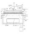
続いてこのようなゲ−ト絶縁膜2の形成方法について説明する。図2はゲ−ト絶縁膜2の成膜に用いられるプラズマ成膜装置であり、3は例えばアルミニウムにより形成された真空容器である。この真空容器3の上面には、基板例えばウエハWよりも大きい開口部30が形成されており、この開口部30を塞ぐように例えば窒化アルミ等の誘電体により構成された偏平な円筒形状のガス供給室4が設けられている。このガス供給室4の下面には多数のガス供給孔41が形成されており、ガス供給室41に導入されたガスが当該ガス供給孔41を介して真空容器3内にシャワ−状に供給されるようになっている。
【0014】
ガス供給室4の外側には、例えば銅により形成された多孔スロット電極50を介して、高周波電源部をなし、例えば2.45GHzのマイクロ波を発生するマイクロ波電源部51に接続された導波路5が設けられている。この導波路5は多孔スロット電極50に下縁が接続された偏平な円形導波管5Aと、この円形導波管5Aの上面に一端側が接続された円筒形導波管5Bと、この円筒形導波管5Bの上面に接続された同軸導波変換器5Cと、この同軸導波変換器5Cの側面に直角に一端側が接続され、他端側がマイクロ波電源部51に接続された矩形導波管5Dとを組み合わせて構成されている。
【0015】
ここで本発明ではUHFとマイクロ波とを含めて高周波領域と呼んでおり、高周波電源部より供給される高周波電力は300MHz以上のUHFや1GHz以上のマイクロ波を含む、300MHz以上2500MHz以下のものとし、これらの高周波電力により発生されるプラズマを高周波プラズマ呼ぶものとする。
【0016】
前記前記円筒形導波管5Bの内部には、導電性材料よりなる軸部52が、一端側が多孔スロット電極50の上面のほぼ中央に接続し、他端側が円筒形導波管5Bの上面に接続するように同軸状に設けられており、これにより当該導波管5Bは同軸導波管として構成されている。
【0017】
前記多孔スロット電極50は、前記開口部30よりも大きい円板に、マイクロ波を透過するのための多数のスロット50aを同心円上に形成して構成されており、スロット50aの長さや配列間隔は、マイクロ波電源部51より発生したマイクロ波の波長に応じて決定されている。
【0018】
真空容器3の上部側の側壁には例えばその周方向に沿って均等に配置した16か所の位置にガス供給管42が設けられており、このガス供給管42から希ガス及びNを含むガスが真空容器3のプラズマ領域P近傍にムラなく均等に供給されるようになっている。
【0019】
また真空容器3内には、ガス供給室4と対向するようにウエハWの載置台31が設けられている。この載置台31には図示しない温調部が内蔵されており、これにより当該載置台31は熱板として作用するように構成されている。さらに真空容器3の底部には排気管32の一端側が接続されており、この排気管32の他端側は真空ポンプ33に接続されている。
【0020】
次に上述の装置を用いてウエハW上にゲ−ト絶縁膜2よりなる絶縁膜を形成する方法について説明する。先ず真空容器3の側壁に設けた図示しないゲ−トバルブを開いて図示しない搬送ア−ムにより、例えばシリコン基板1表面にフィ−ルド酸化膜11が形成されたウエハWを載置台31上に載置する。
【0021】
続いてゲ−トバルブを閉じて内部を密閉した後、真空ポンプ33により排気管32を介して内部雰囲気を排気して所定の真空度まで真空引きし、所定の圧力に維持する。一方マイクロ波電源部51より例えば2.45GHz、3kWのマイクロ波を発生させ、このマイクロ波を導波路5により案内して多孔スロット電極50及びガス供給室4を介して真空容器3内に導入し、これにより真空容器3内の上部側のプラズマ領域Pにて高周波プラズマを発生させる。
【0022】
ここでマイクロ波は矩形導波管5D内を矩形モ−ドで伝送し、同軸導波変換器5Cにて矩形モ−ドから円形モ−ドに変換され、円形モ−ドで円筒形同軸導波管5Bを伝送し、さらに円形導波管5Aにて拡げられた状態で伝送していき、多孔スロット電極50のスロット50aより放射され、ガス供給室4を透過して真空容器3に導入される。この際マイクロ波を用いているので高密度のプラズマが発生し、またマイクロ波を多孔スロット電極50の多数のスロット50aから放射しているのでプラズマが高密度なものとなる。
【0023】
そして載置台31の温度を調節してウエハWを例えば400℃に加熱しながら、ガス供給管42より第1のガスであるXeガスと、N2 ガスと、H2 ガスとを、夫々500sccm、25sccm、15sccmの流量で導入して第1の工程を実施する。この工程では、導入されたガスは真空容器3にて発生したプラズマ流により活性化(プラズマ化)され、このプラズマにより図3(a)に示すように、シリコン基板1の表面が窒化されて第1のSiN膜21が形成される。こうしてこの窒化処理を例えば2分行い、20オングストロ−ムの厚さの第1のSiN膜21を形成する。
【0024】
次いでマイクロ波電源部51よりの例えば2.45GHz、200Wのマイクロ波を導入し、真空容器3内にてプラズマを発生させると共に、ウエハ温度が例えば400℃、プロセス圧力が例えば50mTorr〜1Torrの状態で、真空容器3内に第2のガスを導入して第2の工程を実施する。つまりガス供給室4よりSiを含むガス例えばSiH4 ガスを例えば15sccmの流量で導入すると共に、ガス供給管42よりXeガスと、N2 ガスとを、夫々500sccm、20sccmの流量で導入する。
【0025】
この工程では、導入された第2のガスは真空容器3にて発生したプラズマ流によりプラズマ化され、このプラズマにより図3(b)に示すように、第1のSiN膜21の表面に第2のSiN膜22が形成される。このSiN膜22は成膜速度が例えば20オングストロ−ム/分であるので、この成膜処理を例えば1分行い、20オングストロ−ムの厚さの第2のSiN膜22を形成する。このようにしてト−タル3分間で40オングストロ−ムの厚さのゲ−ト絶縁膜2を形成する。 上述の第1の工程では、上述のプロセス成膜装置にて高密度のプラズマを発生させ、このプラズマにより希ガスとNとHとを含み、Siを含まないガスであって、希ガスの含有量が50%以上99%以下である第1のガスをプラズマ化し、これにより例えば300〜400℃の温度に加熱されたシリコン基板1の表面を窒化して第1のSiN膜21を形成しているので、電気的特性の良好な第1のSiN膜21を得ることができる。
【0026】
ここで絶縁膜の電気的特性は欠陥の数で決定され、欠陥数が少ない程電気的特性は良好であるが、上述の方法にて形成される第1のSiN膜21の欠陥の数は7×10¹⁰個/cm2 程度であって、1×10¹²個/cm2 程度の数の欠陥がある熱窒化膜に比べて少ないので、電気的特性は良好であるといえる。
【0027】
このように上述の方法により形成された第1のSiN膜21の電気的特性が良好である理由は次のように考えられる。先ず第1のガスは、希ガスとNとHとを含み、Siを含まないガスであるが、希ガスを導入することにより、界面順位密度などの欠陥の発生が抑えられるためと推察される。この際後述の実験で明らかなように、希ガスの含有量が50%よりも少ないと欠陥数が多くなる。また100%とすると成膜ができなくなるが、99%以下であれば成膜速度は小さくなるものの膜質を悪化させることなく成膜を行うことができるので、50%以上99%以下とすることが望ましい。またHを含むガスを導入することにより、ダングリングボンドを減少させることができ、これにより欠陥の発生が抑えられるので、より電気的特性が良好になると考えられる。
【0028】
さらに例えばICP(Inductive Coupled Plasma)などと呼ばれている、ド−ム状の容器に巻かれたコイルにより電界及び磁界を与えてプラズマを生成させる方法により発生されたプラズマに第1のガスをプラズマ化した場合には、得られるSiN膜の欠陥数が多くなったことから、上述のプラズマ成膜装置にて、既述のように高密度のプラズマを発生させ、このプラズマにより第1のガスをプラズマ化することにより、電気的特性を向上させることができると考えられる。
【0029】
上述の第2の工程では、上述のプロセス成膜装置にて高密度のプラズマを発生させ、このプラズマにより希ガスとNとSiを含む第2のガスのプラズマにより第2のSiN膜22を形成しているので、第1のSiN膜21よりも成膜速度の大きい第2のSiN膜22を得ることができる。
【0030】
このように成膜速度が大きくなるのは、Siを含むガス例えばSiH4 などのシラン系のガスを導入しているためであるが、同時に希ガスを導入しているのは、成膜速度が速くなり過ぎると膜厚の制御が困難になるので、シラン系ガスの濃度を低くするためである。ここで不活性ガスの量は、多過ぎると成膜速度が小さくなり、少な過ぎると膜の欠陥数が多くなるので50%以上99%以下とすることが望ましい。
【0031】
また上述のプロセスでは第2のSiN膜22の成膜の際に、マイクロ波の電力を200Wと第1のSiN膜21を形成する場合(3kW)よりも小さくしているが、このようにするのはSiH4 の分解により生成したH2 が外側に広がっていき、このH2 により外側の領域では中央領域よりもSiの濃度が低くなって、この結果SiN膜22の膜質の均一性が悪くなってしまうので、これを防止するためにマイクロ波の電力を小さくしてSiH4 の過度の分解を抑えているからである。
【0032】
さらに上述のプロセスでは、第1の工程と第2の工程とを同じプラズマ成膜装置を用いて行っているので、第1の工程と第2の工程とを連続して行うことができてト−タルの成膜時間を短縮することができ、これによりスル−プットを向上させることができる。また上述のプラズマ成膜装置は電子温度が低いので、この装置を用いて第1のSiN膜21や第2のSiN膜22を形成することにより、シリコン基板1に与えるダメ−ジを小さくすることができる。
【0033】
ところで上述の方法で形成される第2のSiN膜22は1×10¹¹個/cm2 程度の欠陥があり、第1のSiN膜21よりも電気的特性が悪いが、電気的に良好な特性が必要な部分はSiN膜がシリコン基板に接している部分であって、必ずしも膜全体に亘って電気的に良好であることが必要ではないので、このような第2のSiN膜22をシリコン基板1との界面より上層に形成する場合には、ゲ−ト絶縁膜2の電気的特性に悪影響は与えない。
【0034】
このように上述のプロセスでは、ゲ−ト絶縁膜2を、電気的特性の良い第1のSiN膜21と、第1のSiN膜21よりも成膜速度の大きい第2のSiN膜22とを積層して形成したので、電気的特性の良好な絶縁膜を短い成膜時間で形成することができる。
【0035】
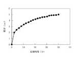
具体的には、例えば上述の第1の工程のプロセスのように、Xeガス/N2 ガス/H2 ガス=500sccm/25sccm/15sccmの第1のガスによるシリコン基板1の窒化処理を行うと、図4に示すように、最初の2分間で2nm(20オングストロ−ム)のSiN膜が形成でき、処理の初期には大きな速度で形成できるものの、膜厚が2nmを越えると形成速度が小さくなっていき、4nmの窒化膜が必要な場合、処理時間に約20分かかってしまう。一方第2の工程のプロセスのように、SiH4 ガス/N2 ガス/Xeガス=15sccm/20sccm/500sccmの第2のガスをプラズマ化してSiN膜を形成すると、毎分2nmの速度で成膜を行うことができる。
【0036】
従って4nmの膜厚のシリコン窒化膜が必要な場合には、図5に示すように、第1のガスによる窒化処理を2分間行って、シリコン基板1との界面に第1のSiN膜21を2nm形成し、次いで第2のガスによる成膜処理を1分間行って、第1のSiN膜22の上面へ2nmの厚さの第2のSiN膜22を形成することにより、結果として膜厚4nmのSiN膜を3分間で形成することができる。
【0037】
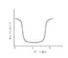
またこうして上述のプロセスにて得られたゲ−ト絶縁膜2についてキャパシタンスとゲ−ト電圧との関係を測定したところ、図6に示す電気的特性が得られ、膜厚が4nmと薄い場合であっても、従来用いられていたSiO2 膜と電気的に同等であることが認められた。
【0038】
さらに上述のプラズマ成膜装置にて、第1のガスとして、ArガスとN2 ガスとH2 ガスとを90:7:3の割合で混合したガス(Ar/N2 /H2 =450sccm/35sccm/15sccm)を用いて、ウエハ温度400℃、プロセス圧力50mTorr〜1Torrの下、マイクロ波電源部51から2.45GHz,3kWのマイクロ波電力を導入して上述と同様に第1の工程を行って、20オングストロ−ムの厚さの第1のSiN膜21を形成し、次いで第2のガスとして、SiH4 ガスとN2 ガスとArガスとを3:4:90の割合で混合したガス(SiH4 /N2 /Ar=15sccm/20sccm/450sccm)を用いて、ウエハ温度400℃、プロセス圧力50mTorrの下、マイクロ波電源部から2.45GHz,200Wのマイクロ波電力を導入して第2の工程を行い、20オングストロ−ムの厚さの第2のSiN膜23を形成したところ、ト−タルの成膜時間は4分であった。また得られた絶縁膜について電気的特性を測定したところ、膜厚が40オングストロ−ムと薄い場合であっても電気的に良好であり、ゲ−ト絶縁膜に適していることが認められた。
【0039】
続いて第1のガスの不活性ガスの割合の最適化を図るために行った実験例について説明する。第1のガスとしてXeガスとN2 ガスとH2 ガスとを用い、上述のプラズマ成膜装置にて、ウエハ温度400℃、プロセス圧力50mTorr〜1Torrの下、マイクロ波電源部51から2.45GHz,3kWのマイクロ波電力を導入して20オングストロ−ムの厚さの第1のSiN膜21を形成した。この際N2 ガスとH2 ガスの流量を5:2の割合として、Xeガスの量を30%〜99%の範囲で変えて第1のSiN膜21を形成し、その欠陥の数をCV測定法により測定し、その数に応じて電気的特性を評価した。この結果を図7に示すが、電気的特性は○、△、×の三段階で評価した。
【0040】
この結果Xeガスが50%〜99%の場合には、欠陥数は7×10¹⁰個/cm2 程度であって電気的特性が良好であるが、40%以下の場合には欠陥数が多くなり、電気的特性が悪化することが確認された。
【0041】
以上において第1のガスに含まれる希ガスとしては、Xe以外にヘリウム(He),ネオン(Ne),アルゴン(Ar),クリプトン(Kr)等を用いることができ、第1のガスとして希ガスとNH3 とを含むガスを用いてもよい。また第2のガスとしては、希ガスとNとSiを含むガスが用いられるが、Siを含むガスとしてはSiH4 以外にSi2 H6 を用いてもよい。
【0042】
また上述のプラズマ成膜装置では、2.45GHzのマイクロ波を使用する例について説明したが、本発明では例えば500MHzのUHFを用いてプラズマを発生させるようにしてもよく、この場合には周波数に合せて多孔スロット電極のスロットを長穴に設定する。
【0043】
次に本発明の他の例について説明する。この例は絶縁膜の第1の膜21をSiO2 膜により形成したものであり、このSiO2 膜は例えば上述のプラズマ成膜装置にて、希ガスと酸素(O)とを含み、Siを含まないガスであって、希ガスの含有量が50%以上99%以下のガスのプラズマにより、シリコン基板1の表面をプラズマ酸化することにより形成される。
【0044】
具体的には希ガスとOとを含み、Siを含まないガスであって、希ガスの含有量が50%以上99%以下のガスとして、ArガスとO2 ガスの混合ガスを用い、これらのガスをArガス/O2 ガス=500sccm/15sccmの流量で導入して、ウエハ温度430℃、プロセス圧力50mTorr〜1Torrの下、マイクロ波電源部から2.45GHz,3kWのマイクロ波電力を導入して、ArガスとO2 ガスをプラズマ化し、このプラズマによりシリコン基板1の表面を2分間酸化処理して例えば20オングストロ−ムの厚さのSiO2 膜を形成する。そして得られたSiO2 膜の上に上述と同様のプロセスで第2のSiN膜22を例えば20オングストロ−ム形成することにより絶縁膜を形成する。
【0045】
このプロセスでは例えばト−タル3分間で40オングストロ−ムの絶縁膜を成膜することができ、またシリコンのプラズマ酸化により形成されたSiO2 膜は、欠陥の数が7×10¹⁰個/cm2 と少ないので電気的特性が良好である。ここで不活性ガスの含有量は50%以上99%以下であることが望ましいが、これは50%よりも少なくなると界面順位密度が増加するからである。
【0046】
実際に上述のプロセスで絶縁膜を形成し、キャパシタンスとゲ−ト電圧との関係を測定したところ良好な結果が得られ、ゲ−ト絶縁膜として適していることが認められた。これにより第1の膜21としてSiO2 膜を用いてト−タルの膜厚が40オングストロ−ムと薄い絶縁膜を形成する場合であっても、SiO2 膜の上に第2の膜22を積層することによってリ−ク電流が小さくなることが理解される。
【0047】
また希ガスとOとを含み、Siを含まないガスとしては、希ガスとオゾン(O3 )との組み合わせや、希ガスと水蒸気(H2 O)との組み合わせを用いるようにしてもよい。
【0048】
次に本発明のさらに他の例について説明する。この例は絶縁膜の第1の膜21をシリコンの熱酸化により形成されたSiO2 膜により形成したものであり、このSiO2 膜は例えば急速熱酸化プロセスにより、シリコンウエハを850℃程度に加熱し、水蒸気雰囲気に晒すことにより形成される。
【0049】
このような第1の膜21を例えば5分間で20オングストロ−ム形成し、この上に上述と同様のプロセスで第2のSiN膜22を例えば20オングストロ−ム形成することにより絶縁膜を形成すると、例えばト−タル6分間で40オングストロ−ムの絶縁膜を成膜することができる。またシリコンの熱酸化により形成されたSiO2 膜は、欠陥の数が5×10¹⁰個/cm2 と少ないので電気的特性が非常に良好である。実際に上述のプロセスで絶縁膜を形成し、キャパシタンスとゲ−ト電圧との関係を測定したところ良好な結果が得られ、ゲ−ト絶縁膜として適していることが認められた。
【0050】
次に本発明のさらにまた他の例について説明する。この例は絶縁膜の第1の膜21をシリコン酸窒化膜により形成したものであり、このシリコン酸窒化膜は例えばSiO2 膜をNO雰囲気中でアニ−ルすることにより形成される。具体的には、20オングストロ−ムの厚みのシリコン酸化膜を持つシリコンウエハを850℃に加熱し、NOガスに晒すことにより熱窒化膜を形成する。
【0051】
このプロセスにより、シリコン基板1の表面に10分間で例えば20オングストロ−ムの厚さのシリコン酸窒化膜を形成し、この上に上述と同様のプロセスで第2のSiN膜22を例えば20オングストロ−ム形成することにより40オングストロ−ムの絶縁膜を形成する。
【0052】
このプロセスでは例えばト−タル11分間で絶縁膜を形成することができ、また上述のプロセスで形成されたシリコン酸窒化膜は、欠陥の数が5×10¹⁰個/cm2 程度であって電気的特性が良好である。実際に上述のプロセスで絶縁膜を形成し、キャパシタンスとゲ−ト電圧との関係を測定したところ良好な結果が得られ、この絶縁膜がゲ−ト絶縁膜として適していることが認められた。
【0053】
【発明の効果】
以上のように本発明によれば、電気的特性の良い第1の膜と成膜速度の大きい第2の膜とを積層して絶縁膜を形成しているので、電気的特性のよい絶縁膜を短時間で形成することができる。
【図面の簡単な説明】
【図1】本発明方法によって製造される半導体装置の構造の一例を示す断面図である。
【図2】本発明方法を実施するためのプラズマ成膜装置の一例を示す断面図である。
【図3】本発明方法を用いて半導体装置を製造する場合の工程図を説明する。
【図4】処理時間と膜厚との関係を示す特性図である。
【図5】処理時間と膜厚との関係を示す特性図である。
【図6】キャパシタンスとゲ−ト電圧との関係を示す特性図である。
【図7】Xeガスの量と電気的特性との関係を示す特性図である。
【符号の説明】
1 シリコン基板
2 ゲ−ト絶縁膜
21 第1の膜
22 第2の膜
4 ガス供給室
42 ガス供給管
5 導波路
51 マイクロ波電源部
50 多孔スロットアンテナ
W 半導体ウエハ
P プラズマ領域[0001]
BACKGROUND OF THE INVENTION
The present invention relates to a method for manufacturing a semiconductor device provided with an insulating film such as a gate insulating film on the surface of a silicon substrate.
[0002]
[Prior art]
In a silicon semiconductor device, a silicon oxide film (SiO2 film) is conventionally used as a gate insulating film. However, if it is attempted to make the SiO2 film thinner than the currently used film thickness of 60 angstroms, the limit is 40 angstroms. If the film thickness is further reduced, the leakage current increases and the power consumption increases. And not suitable for practical use.
[0003]
Therefore, it has been studied to use a silicon nitride film (SiN film) as a gate insulating film, which does not increase the leak current even if it is thinned to about 40 angstroms. For example, JP-A-5-36899 and JP-A-9-50996 propose an example in which a silicon nitride film formed by thermal nitriding and a silicon nitride film formed by vapor deposition are used in a stacked manner. In the example of No. 1, polycrystalline silicon is patterned into a predetermined shape to form an electrode, and then rapid thermal nitridation is performed at 850 ° C. for 60 seconds using an annealing apparatus, and a film thickness of several nm is formed on the surface of the electrode. A silicon nitride film is formed by thermal nitridation to the extent that a silicon nitride film is deposited on the surface of the silicon nitride film by a reduced pressure vapor phase growth method to a thickness of about 4 nm.
[0004]
Japanese Patent Laid-Open No. 6-61470 proposes an example using a silicon oxynitride film. In this example, the silicon oxide film is annealed at 900 to 1000 ° C. for about 10 minutes to 1 hour in an NH 3 atmosphere. Thus, a silicon oxynitride film is formed.
[0005]
Further, Japanese Patent Laid-Open No. 10-178159 proposes an example using a three-layer film made of a silicon oxynitride film, a silicon nitride film, and a silicon oxynitride film. In this example, a silicon oxynitride film is formed with monosilane and nitrous oxide in a low pressure CVD apparatus under a film forming condition of about 50 Pa and 700 to 850 ° C., and then nitrous oxide is formed at 700 to 850 ° C. Then, the high-temperature silicon oxide film is changed to a silicon oxynitride film, and the silicon nitride film is formed at 700 to 850 ° C. with dichlorosilane and ammonia by a low pressure CVD apparatus.
[0006]
[Problems to be solved by the invention]
However, a silicon nitride film formed by thermal nitriding has a problem that it has many dangling bonds (unbonded species) and has poor electrical characteristics. Further, the silicon nitride film (silicon nitride film) formed by the low pressure vapor phase growth method has a problem that the electric characteristics are bad, and further, the silicon oxynitride film has a problem that it takes time to form.
[0007]
In view of this, the present inventors have studied using high-density plasma to convert a mixed gas of argon gas, nitrogen gas, and hydrogen gas into plasma, and nitriding the silicon substrate surface with this plasma to form a SiN film. However, although this method can obtain a SiN film having excellent electrical characteristics, it has a drawback that the deposition rate of the SiN film is low.
[0008]
The present invention has been made under such circumstances, and an object of the present invention is to provide a method of manufacturing a semiconductor device having an insulating film that has excellent electrical characteristics and a high deposition rate.
[0009]
[Means for Solving the Problems]
For this reason, the manufacturing method of the semiconductor device of the present invention is as follows.The step of thermally oxidizing the surface of the silicon substrate to form a silicon oxide film, and then converting the gas containing noble gas, nitrogen, and silicon, and containing noble gas to 50% to 99% into plasma, And a step of forming a silicon nitride film on the surface of the silicon oxide film. .
[0011]
First, an example of the structure of a semiconductor device manufactured by the method of the present invention will be described with reference to FIG. 1, taking as an example a semiconductor device provided with a gate insulating film as an insulating film. In the figure, 1 is a silicon substrate, 11 is a field oxide film, 2 is a gate insulating film, and 13 is a gate electrode. The present invention is characterized by the
[0012]
In this example, the
[0013]
Next, a method for forming such a
[0014]
A waveguide connected to a
[0015]
Here, in the present invention, UHF and microwaves are referred to as a high-frequency region, and high-frequency power supplied from a high-frequency power supply unit is 300 MHz to 2500 MHz including 300 MHz or more UHF or 1 GHz or more microwaves. The plasma generated by these high frequency powers is called high frequency plasma.
[0016]
Inside the cylindrical waveguide 5B, a
[0017]
The
[0018]
For example,
[0019]
A mounting table 31 for the wafer W is provided in the
[0020]
Next, a method for forming an insulating film made of the
[0021]
Subsequently, after closing the gate valve and sealing the inside, the internal atmosphere is evacuated through the
[0022]
Here, the microwave is transmitted through the
[0023]
Then, while adjusting the temperature of the mounting table 31 and heating the wafer W to 400 ° C., for example, the Xe gas,
[0024]
Next, a microwave of 2.45 GHz, 200 W, for example, from the microwave
[0025]
In this step, the introduced second gas is turned into plasma by the plasma flow generated in the
[0026]
Here, the electrical characteristics of the insulating film are determined by the number of defects. The smaller the number of defects, the better the electrical characteristics. However, the number of defects in the
[0027]
The reason why the
[0028]
Further, for example, a first gas is applied to plasma generated by a method of generating plasma by applying an electric field and a magnetic field by a coil wound around a dome-shaped container, which is called ICP (Inductive Coupled Plasma). In this case, since the number of defects in the obtained SiN film is increased, the above-described plasma film forming apparatus generates high-density plasma as described above, and the first gas is generated by this plasma. It is considered that the electrical characteristics can be improved by converting into plasma.
[0029]
In the above-described second step, high-density plasma is generated by the above-described process film formation apparatus, and the
[0030]
The reason why the film formation rate increases in this way is that a gas containing Si, for example, a silane-based gas such as SiH4 is introduced. At the same time, a rare gas is introduced because the film formation rate is high. This is because the control of the film thickness becomes difficult if it becomes too much, so that the concentration of the silane-based gas is lowered. Here, if the amount of the inert gas is too large, the film forming rate is reduced, and if it is too small, the number of defects in the film increases.
[0031]
Further, in the above-described process, when the
[0032]
Furthermore, in the above-described process, since the first step and the second step are performed using the same plasma film forming apparatus, the first step and the second step can be performed continuously. -The film formation time of the tar can be shortened, whereby the throughput can be improved. In addition, since the above-described plasma film forming apparatus has a low electron temperature, the
[0033]
By the way, the
[0034]
Thus, in the above-described process, the
[0035]
Specifically, when the
[0036]
Therefore, when a silicon nitride film having a thickness of 4 nm is required, as shown in FIG. 5, nitriding treatment with the first gas is performed for 2 minutes to form the
[0037]
Further, when the relationship between the capacitance and the gate voltage was measured for the
[0038]
Further, in the above-described plasma film forming apparatus, a gas in which Ar gas, N2 gas, and H2 gas are mixed at a ratio of 90: 7: 3 (Ar / N2 / H2 = 450 sccm / 35 sccm / 15 sccm) as the first gas. Is used, and a microwave power of 2.45 GHz and 3 kW is introduced from the
[0039]
Next, an experimental example performed to optimize the ratio of the inert gas in the first gas will be described. Xe gas, N2 gas, and H2 gas are used as the first gas, and 2.45 GHz, 3 kW from the microwave
[0040]
As a result, when the Xe gas is 50% to 99%, the number of defects is about 7 × 10 10 pieces /
[0041]
In the above, as the rare gas contained in the first gas, helium (He), neon (Ne), argon (Ar), krypton (Kr), or the like can be used in addition to Xe, and the rare gas can be used as the first gas. A gas containing NH3 may be used. As the second gas, a gas containing a rare gas and N and Si is used. However, as a gas containing Si, Si2 H6 may be used in addition to SiH4.
[0042]
In the plasma film forming apparatus described above, an example in which a microwave of 2.45 GHz is used has been described. However, in the present invention, plasma may be generated using, for example, 500 MHz UHF. In addition, the slot of the porous slot electrode is set to be a long hole.
[0043]
Next, another example of the present invention will be described. In this example, the
[0044]
Specifically, a gas containing noble gas and O, not containing Si, and having a rare gas content of 50% to 99%, a mixed gas of Ar gas and O2 gas is used. A gas is introduced at a flow rate of Ar gas / O2 gas = 500 sccm / 15 sccm, and a microwave power of 2.45 GHz and 3 kW is introduced from a microwave power source under a wafer temperature of 430 ° C. and a process pressure of 50 mTorr to 1 Torr, Ar gas and O2 gas are converted into plasma, and the surface of the
[0045]
In this process, for example, an insulating film of 40 angstroms can be formed in a total of 3 minutes, and the number of defects is as small as 7 × 10 10 /
[0046]
When an insulating film was actually formed by the above-described process and the relationship between the capacitance and the gate voltage was measured, good results were obtained, and it was confirmed that the film was suitable as a gate insulating film. As a result, even if an
[0047]
Further, as the gas containing noble gas and O and not containing Si, a combination of noble gas and ozone (O3) or a combination of noble gas and water vapor (H2 O) may be used.
[0048]
Next, still another example of the present invention will be described. In this example, the
[0049]
When an insulating film is formed by forming such a
[0050]
Next, still another example of the present invention will be described. In this example, the
[0051]
By this process, a silicon oxynitride film having a thickness of, for example, 20 angstroms is formed on the surface of the
[0052]
In this process, for example, an insulating film can be formed in a total of 11 minutes, and the silicon oxynitride film formed by the above-described process has a number of defects of about 5 × 10 10 /
[0053]
【The invention's effect】
As described above, according to the present invention, since the insulating film is formed by laminating the first film having good electrical characteristics and the second film having a high deposition rate, the insulating film having good electrical characteristics. Can be formed in a short time.
[Brief description of the drawings]
FIG. 1 is a cross-sectional view showing an example of the structure of a semiconductor device manufactured by a method of the present invention.
FIG. 2 is a cross-sectional view showing an example of a plasma film forming apparatus for carrying out the method of the present invention.
FIG. 3 is a process chart in the case of manufacturing a semiconductor device using the method of the present invention.
FIG. 4 is a characteristic diagram showing the relationship between processing time and film thickness.
FIG. 5 is a characteristic diagram showing the relationship between processing time and film thickness.
FIG. 6 is a characteristic diagram showing the relationship between capacitance and gate voltage.
FIG. 7 is a characteristic diagram showing the relationship between the amount of Xe gas and electrical characteristics.
[Explanation of symbols]
1 Silicon substrate
2 Gate insulation film
21 First membrane
22 Second membrane
4 Gas supply room
42 Gas supply pipe
5 Waveguide
51 Microwave power supply
50 Porous slot antenna
W Semiconductor wafer
P Plasma region
Claims (1)
Translated fromJapanese次いで希ガスと窒素とシリコンとを含み、希ガスの含有量が50%以上99%以下のガスをプラズマ化して、このプラズマにより前記シリコン酸化膜の表面にシリコン窒化膜を形成する工程と、を含むことを特徴とする半導体装置の製造方法。Forming a silicon oxide film by thermally oxidizing the surface of thesilicon substrate ;
Next, a step of forming a silicon nitride film on the surface of the silicon oxide film by plasma-forming a gas containing noble gas, nitrogen and silicon and containing no less than 50% and no more than 99% of the noble gas. A method for manufacturing a semiconductor device, comprising:
Priority Applications (6)
| Application Number | Priority Date | Filing Date | Title |
|---|---|---|---|
| JP06345599AJP4119029B2 (en) | 1999-03-10 | 1999-03-10 | Manufacturing method of semiconductor device |
| KR1020000010968AKR100745495B1 (en) | 1999-03-10 | 2000-03-06 | Semiconductor manufacturing method and semiconductor manufacturing apparatus |
| US09/521,601US6399520B1 (en) | 1999-03-10 | 2000-03-09 | Semiconductor manufacturing method and semiconductor manufacturing apparatus |
| US10/123,485US6470824B2 (en) | 1999-03-10 | 2002-04-17 | Semiconductor manufacturing apparatus |
| KR1020060044607AKR100856531B1 (en) | 1999-03-10 | 2006-05-18 | Semiconductor fabrication method and semiconductor fabrication equipment |
| KR1020080019058AKR100943246B1 (en) | 1999-03-10 | 2008-02-29 | Semiconductor manufacturing method and semiconductor manufacturing apparatus |
Applications Claiming Priority (1)
| Application Number | Priority Date | Filing Date | Title |
|---|---|---|---|
| JP06345599AJP4119029B2 (en) | 1999-03-10 | 1999-03-10 | Manufacturing method of semiconductor device |
Related Child Applications (1)
| Application Number | Title | Priority Date | Filing Date |
|---|---|---|---|
| JP2007248069ADivisionJP2008066736A (en) | 2007-09-25 | 2007-09-25 | Method for manufacturing semiconductor device |
Publications (2)
| Publication Number | Publication Date |
|---|---|
| JP2000260767A JP2000260767A (en) | 2000-09-22 |
| JP4119029B2true JP4119029B2 (en) | 2008-07-16 |
Family
ID=13229739
Family Applications (1)
| Application Number | Title | Priority Date | Filing Date |
|---|---|---|---|
| JP06345599AExpired - LifetimeJP4119029B2 (en) | 1999-03-10 | 1999-03-10 | Manufacturing method of semiconductor device |
Country Status (1)
| Country | Link |
|---|---|
| JP (1) | JP4119029B2 (en) |
Families Citing this family (18)
| Publication number | Priority date | Publication date | Assignee | Title |
|---|---|---|---|---|
| JP4105353B2 (en) | 1999-07-26 | 2008-06-25 | 財団法人国際科学振興財団 | Semiconductor device |
| JP4991577B2 (en)* | 1999-07-26 | 2012-08-01 | 公益財団法人国際科学振興財団 | Method for forming silicon oxide film, semiconductor device and method for manufacturing the same |
| JP4987206B2 (en)* | 2000-03-13 | 2012-07-25 | 公益財団法人国際科学振興財団 | Method for manufacturing flash memory device |
| JP4713752B2 (en)* | 2000-12-28 | 2011-06-29 | 財団法人国際科学振興財団 | Semiconductor device and manufacturing method thereof |
| JP5068402B2 (en) | 2000-12-28 | 2012-11-07 | 公益財団法人国際科学振興財団 | Dielectric film and method for forming the same, semiconductor device, nonvolatile semiconductor memory device, and method for manufacturing semiconductor device |
| KR20070116696A (en)* | 2001-01-22 | 2007-12-10 | 동경 엘렉트론 주식회사 | Manufacturing Method and Plasma Processing Method of Electronic Device Material |
| CN101752244B (en)* | 2001-01-25 | 2012-02-08 | 东京毅力科创株式会社 | Plasma treatment method |
| JP2003060198A (en)* | 2001-08-10 | 2003-02-28 | Matsushita Electric Ind Co Ltd | Semiconductor device and manufacturing method thereof |
| JP2003100742A (en)* | 2001-09-27 | 2003-04-04 | Hitachi Kokusai Electric Inc | Method for manufacturing semiconductor device |
| KR20060118620A (en) | 2001-12-26 | 2006-11-23 | 동경 엘렉트론 주식회사 | Substrate processing method and semiconductor device manufacturing method |
| JP4694782B2 (en)* | 2002-12-02 | 2011-06-08 | 財団法人国際科学振興財団 | Semiconductor device, manufacturing method thereof, and semiconductor surface processing method |
| SG124265A1 (en) | 2002-12-02 | 2006-08-30 | Tadahiro Ohmi | Semiconductor device and method of manufacturing the same |
| JP2007165480A (en)* | 2005-12-12 | 2007-06-28 | Matsushita Electric Ind Co Ltd | Semiconductor device and manufacturing method thereof |
| US8006640B2 (en) | 2006-03-27 | 2011-08-30 | Tokyo Electron Limited | Plasma processing apparatus and plasma processing method |
| CN101454880B (en) | 2006-05-31 | 2012-05-02 | 东京毅力科创株式会社 | Plasma CVD method, method for forming silicon nitride film, method for manufacturing semiconductor device, and plasma CVD apparatus |
| US7985695B2 (en) | 2007-09-28 | 2011-07-26 | Canon Kabushiki Kaisha | Forming silicon oxide film from RF plasma of oxidizing gas |
| KR20180044432A (en)* | 2015-09-18 | 2018-05-02 | 어플라이드 머티어리얼스, 인코포레이티드 | Low-temperature conformal deposition of silicon nitride on high aspect ratio structures |
| JP2022002246A (en)* | 2020-06-19 | 2022-01-06 | 東京エレクトロン株式会社 | Deposition method and plasma processing apparatus |
- 1999
- 1999-03-10JPJP06345599Apatent/JP4119029B2/ennot_activeExpired - Lifetime
Also Published As
| Publication number | Publication date |
|---|---|
| JP2000260767A (en) | 2000-09-22 |
Similar Documents
| Publication | Publication Date | Title |
|---|---|---|
| KR100856531B1 (en) | Semiconductor fabrication method and semiconductor fabrication equipment | |
| JP4119029B2 (en) | Manufacturing method of semiconductor device | |
| JP3916565B2 (en) | Manufacturing method of electronic device material | |
| JP4334225B2 (en) | Manufacturing method of electronic device material | |
| JP4255563B2 (en) | Semiconductor manufacturing method and semiconductor manufacturing apparatus | |
| JP4429300B2 (en) | Manufacturing method of electronic device material | |
| JP4408653B2 (en) | Substrate processing method and semiconductor device manufacturing method | |
| US7622402B2 (en) | Method for forming underlying insulation film | |
| US20080274370A1 (en) | Method for Forming Insulation Film | |
| US20050136610A1 (en) | Process for forming oxide film, apparatus for forming oxide film and material for electronic device | |
| JP2005150637A (en) | Processing method and apparatus | |
| TW200836262A (en) | Method for forming insulating film and method for manufacturing semiconductor device | |
| JP4083000B2 (en) | Insulating film formation method | |
| JP2008066736A (en) | Method for manufacturing semiconductor device | |
| JP4850861B2 (en) | Insulating film forming method, insulating film forming apparatus, and plasma processing unit | |
| JP2011165743A (en) | Method of manufacturing semiconductor-device | |
| CN118692986A (en) | Method for manufacturing dielectric layer between isolation chips and isolation chips | |
| JPS58185763A (en) | Nitride film production equipment |
Legal Events
| Date | Code | Title | Description |
|---|---|---|---|
| A621 | Written request for application examination | Free format text:JAPANESE INTERMEDIATE CODE: A621 Effective date:20060223 | |
| A977 | Report on retrieval | Free format text:JAPANESE INTERMEDIATE CODE: A971007 Effective date:20060731 | |
| A131 | Notification of reasons for refusal | Free format text:JAPANESE INTERMEDIATE CODE: A131 Effective date:20070724 | |
| A521 | Written amendment | Free format text:JAPANESE INTERMEDIATE CODE: A523 Effective date:20070925 | |
| A02 | Decision of refusal | Free format text:JAPANESE INTERMEDIATE CODE: A02 Effective date:20071106 | |
| A521 | Written amendment | Free format text:JAPANESE INTERMEDIATE CODE: A523 Effective date:20071228 | |
| A521 | Written amendment | Free format text:JAPANESE INTERMEDIATE CODE: A523 Effective date:20080219 | |
| A911 | Transfer to examiner for re-examination before appeal (zenchi) | Free format text:JAPANESE INTERMEDIATE CODE: A911 Effective date:20080226 | |
| TRDD | Decision of grant or rejection written | ||
| A01 | Written decision to grant a patent or to grant a registration (utility model) | Free format text:JAPANESE INTERMEDIATE CODE: A01 Effective date:20080415 | |
| A61 | First payment of annual fees (during grant procedure) | Free format text:JAPANESE INTERMEDIATE CODE: A61 Effective date:20080424 | |
| R150 | Certificate of patent or registration of utility model | Free format text:JAPANESE INTERMEDIATE CODE: R150 | |
| FPAY | Renewal fee payment (event date is renewal date of database) | Free format text:PAYMENT UNTIL: 20110502 Year of fee payment:3 | |
| FPAY | Renewal fee payment (event date is renewal date of database) | Free format text:PAYMENT UNTIL: 20110502 Year of fee payment:3 | |
| FPAY | Renewal fee payment (event date is renewal date of database) | Free format text:PAYMENT UNTIL: 20140502 Year of fee payment:6 | |
| R250 | Receipt of annual fees | Free format text:JAPANESE INTERMEDIATE CODE: R250 | |
| R250 | Receipt of annual fees | Free format text:JAPANESE INTERMEDIATE CODE: R250 | |
| EXPY | Cancellation because of completion of term |