JP4118659B2 - Substrate tray - Google Patents
Substrate trayDownload PDFInfo
- Publication number
- JP4118659B2 JP4118659B2JP2002346230AJP2002346230AJP4118659B2JP 4118659 B2JP4118659 B2JP 4118659B2JP 2002346230 AJP2002346230 AJP 2002346230AJP 2002346230 AJP2002346230 AJP 2002346230AJP 4118659 B2JP4118659 B2JP 4118659B2
- Authority
- JP
- Japan
- Prior art keywords
- substrate
- tray
- coating
- film
- cleaning
- Prior art date
- Legal status (The legal status is an assumption and is not a legal conclusion. Google has not performed a legal analysis and makes no representation as to the accuracy of the status listed.)
- Expired - Fee Related
Links
Images


Classifications
- H—ELECTRICITY
- H01—ELECTRIC ELEMENTS
- H01L—SEMICONDUCTOR DEVICES NOT COVERED BY CLASS H10
- H01L21/00—Processes or apparatus adapted for the manufacture or treatment of semiconductor or solid state devices or of parts thereof
- H01L21/02—Manufacture or treatment of semiconductor devices or of parts thereof
- H01L21/04—Manufacture or treatment of semiconductor devices or of parts thereof the devices having potential barriers, e.g. a PN junction, depletion layer or carrier concentration layer
- H01L21/18—Manufacture or treatment of semiconductor devices or of parts thereof the devices having potential barriers, e.g. a PN junction, depletion layer or carrier concentration layer the devices having semiconductor bodies comprising elements of Group IV of the Periodic Table or AIIIBV compounds with or without impurities, e.g. doping materials
- H01L21/20—Deposition of semiconductor materials on a substrate, e.g. epitaxial growth solid phase epitaxy
- H—ELECTRICITY
- H01—ELECTRIC ELEMENTS
- H01L—SEMICONDUCTOR DEVICES NOT COVERED BY CLASS H10
- H01L21/00—Processes or apparatus adapted for the manufacture or treatment of semiconductor or solid state devices or of parts thereof
- H01L21/67—Apparatus specially adapted for handling semiconductor or electric solid state devices during manufacture or treatment thereof; Apparatus specially adapted for handling wafers during manufacture or treatment of semiconductor or electric solid state devices or components ; Apparatus not specifically provided for elsewhere
- H01L21/673—Apparatus specially adapted for handling semiconductor or electric solid state devices during manufacture or treatment thereof; Apparatus specially adapted for handling wafers during manufacture or treatment of semiconductor or electric solid state devices or components ; Apparatus not specifically provided for elsewhere using specially adapted carriers or holders; Fixing the workpieces on such carriers or holders
- H01L21/67346—Apparatus specially adapted for handling semiconductor or electric solid state devices during manufacture or treatment thereof; Apparatus specially adapted for handling wafers during manufacture or treatment of semiconductor or electric solid state devices or components ; Apparatus not specifically provided for elsewhere using specially adapted carriers or holders; Fixing the workpieces on such carriers or holders characterized by being specially adapted for supporting a single substrate or by comprising a stack of such individual supports
- B—PERFORMING OPERATIONS; TRANSPORTING
- B05—SPRAYING OR ATOMISING IN GENERAL; APPLYING FLUENT MATERIALS TO SURFACES, IN GENERAL
- B05C—APPARATUS FOR APPLYING FLUENT MATERIALS TO SURFACES, IN GENERAL
- B05C5/00—Apparatus in which liquid or other fluent material is projected, poured or allowed to flow on to the surface of the work
- B05C5/02—Apparatus in which liquid or other fluent material is projected, poured or allowed to flow on to the surface of the work the liquid or other fluent material being discharged through an outlet orifice by pressure, e.g. from an outlet device in contact or almost in contact, with the work
- B05C5/027—Coating heads with several outlets, e.g. aligned transversally to the moving direction of a web to be coated
- B05C5/0275—Coating heads with several outlets, e.g. aligned transversally to the moving direction of a web to be coated flow controlled, e.g. by a valve
- B05C5/0279—Coating heads with several outlets, e.g. aligned transversally to the moving direction of a web to be coated flow controlled, e.g. by a valve independently, e.g. individually, flow controlled
- H—ELECTRICITY
- H01—ELECTRIC ELEMENTS
- H01L—SEMICONDUCTOR DEVICES NOT COVERED BY CLASS H10
- H01L21/00—Processes or apparatus adapted for the manufacture or treatment of semiconductor or solid state devices or of parts thereof
- H01L21/67—Apparatus specially adapted for handling semiconductor or electric solid state devices during manufacture or treatment thereof; Apparatus specially adapted for handling wafers during manufacture or treatment of semiconductor or electric solid state devices or components ; Apparatus not specifically provided for elsewhere
- H01L21/67005—Apparatus not specifically provided for elsewhere
- H01L21/67011—Apparatus for manufacture or treatment
- H01L21/67017—Apparatus for fluid treatment
- H01L21/67028—Apparatus for fluid treatment for cleaning followed by drying, rinsing, stripping, blasting or the like
- H01L21/6704—Apparatus for fluid treatment for cleaning followed by drying, rinsing, stripping, blasting or the like for wet cleaning or washing
- H01L21/67046—Apparatus for fluid treatment for cleaning followed by drying, rinsing, stripping, blasting or the like for wet cleaning or washing using mainly scrubbing means, e.g. brushes
- H—ELECTRICITY
- H01—ELECTRIC ELEMENTS
- H01L—SEMICONDUCTOR DEVICES NOT COVERED BY CLASS H10
- H01L21/00—Processes or apparatus adapted for the manufacture or treatment of semiconductor or solid state devices or of parts thereof
- H01L21/67—Apparatus specially adapted for handling semiconductor or electric solid state devices during manufacture or treatment thereof; Apparatus specially adapted for handling wafers during manufacture or treatment of semiconductor or electric solid state devices or components ; Apparatus not specifically provided for elsewhere
- H01L21/67005—Apparatus not specifically provided for elsewhere
- H01L21/67011—Apparatus for manufacture or treatment
- H01L21/67017—Apparatus for fluid treatment
- H01L21/67028—Apparatus for fluid treatment for cleaning followed by drying, rinsing, stripping, blasting or the like
- H01L21/6704—Apparatus for fluid treatment for cleaning followed by drying, rinsing, stripping, blasting or the like for wet cleaning or washing
- H01L21/67051—Apparatus for fluid treatment for cleaning followed by drying, rinsing, stripping, blasting or the like for wet cleaning or washing using mainly spraying means, e.g. nozzles
Landscapes
- Engineering & Computer Science (AREA)
- Microelectronics & Electronic Packaging (AREA)
- Condensed Matter Physics & Semiconductors (AREA)
- General Physics & Mathematics (AREA)
- Manufacturing & Machinery (AREA)
- Computer Hardware Design (AREA)
- Physics & Mathematics (AREA)
- Power Engineering (AREA)
- Coating Apparatus (AREA)
- Container, Conveyance, Adherence, Positioning, Of Wafer (AREA)
- Application Of Or Painting With Fluid Materials (AREA)
- Formation Of Insulating Films (AREA)
- Exposure Of Semiconductors, Excluding Electron Or Ion Beam Exposure (AREA)
- Materials For Photolithography (AREA)
Description
Translated fromJapanese【0001】
【発明の属する技術分野】
本発明はガラス基板や半導体ウェーハなどの基板の表面に被膜、例えば20μm以上の厚膜を形成する行程で用いるのに適したトレイに関する。
【0002】
【従来の技術】
ガラス基板や半導体ウェーハなどの基板表面にレジスト膜やSOG膜を形成する方法として、回転塗布方式とスリットノズル方式がある。
回転塗布方式はスピンナーで板状被処理物を高速回転させ、板状被処理物の中心に滴下した塗布液を遠心力によって拡散せしめる方式であり、例えば特開平3−56163号公報に開示されている。特に、この先行技術にあっては、スピンナーヘッドの上面に板状被処理物が嵌まり込む凹部を形成している。
また、スリットノズル方式は、米国特許第4,696,885号公報などに開示されており、板状被処理物と同程度の幅を有するスリットノズルから板状被処理物に向けて塗布液をカーテン状に滴下しつつ相対的に移動せしめることで所定範囲に塗膜を形成する方式である。
【0003】
一方最近では基板表面に厚膜を形成する試みがなされている。例えば、ICパターン面上にパンプと称される高さ20μm程度の突起状電極を、集積回路形成技術を応用して形成するには、20μm程度の厚さのレジスト膜を形成する必要がある。
また、従来ではICチップを基板に搭載するのにワイヤボンディングを行っているが、ワイヤボンディングでは金線を1本ずつ繋げなければならず面倒で時間がかかる。そこでワイヤボンディングの代わりにチップ自体に金属柱を複数本設け、この金属柱を介してICチップを基板に搭載するようにしている。この金属柱の高さが100μm程度であり、集積回路形成技術を応用して金属柱を形成するには、100μm程度の厚さのレジスト膜を形成する必要がある。
【0004】
【発明が解決しようとする課題】
回転塗布方式にあっては、供給した塗布液のうち被膜形成に関与する塗布液が5%程度と少なく、殆どが遠心力によって飛散してしまう。また、厚い被膜を得ることができないという課題もある。
さらに、基板(ガラス基板)の寸法はますます大きくなり、その厚みも薄くなる傾向にあり、基板の搬送時等にその自重によって撓んでしまう。
【0005】
一方、スリットノズル方式によれば、塗布液の無駄が少なくなり且つ被膜の膜厚を厚くすることもできる。しかしながら、スリットノズル方式にあっては、塗布開始位置と塗布終了位置における膜厚が表面張力の影響により他の個所に比べて極端に厚くなるという課題がある。
【0006】
また、上述した先行技術はいずれも塗布液を塗布するまでに関するものであり、塗布液を塗布した後、加熱乾燥せしめて被膜を形成し、さらにその後の工程までを含めて効率よく処理を行えるものではない。
【0007】
特に厚膜形成する場合には、基板サイズが大型化した最近では、従来装置では特有の問題が生じる。
即ち、基板上に塗布した塗膜を加熱して乾燥させる際に、塗膜表面が塗膜内部よりも先に乾燥硬化してしまうので、塗膜内部に含有されている溶剤が排出されず塗膜の部位毎に溶剤の残存率が異なり、その結果、高アスペクト比パターンが現像後に基板表面から剥離したり、塗布膜にシワが発生したりする。
また、基板をトレイに載せたまま各工程を搬送するようにすれば、基板の撓みは防止できるが、トレイから基板を持ち上げる際に基板表面に厚膜が形成されているとその重量が加わって基板が撓み破損するおそれがある。
【0008】
【課題を解決するための手段】
上記の各課題を解決すべく、請求項1に記載した基板の搬送と処理に兼用して用いるトレイは、環状をなす外側部材と、この外側部材の開口を塞ぐように取り付けることで基板が嵌まり込む凹部を形成する内側部材とからなり、且つ、内側部材は外側部材に対し厚み方向に位置調整可能とされる構成とした。そして、請求項2に係る発明では前記内側部材には真空吸着と払い出しの際のガス噴出を兼ねる通路が形成された構成とし、請求項3に係る発明では、前記通路と真空源または圧気源とを連結するカプラが設けられている。また、このカプラはトレイの位置決め部材を兼ねる構成とした。このようにトレイの構造に工夫を凝らすことで、各種基板に対応でき、トレイからの基板の払い出し時の破損を防止でき、異なる装置間を移動する際の位置決めも容易になる。
【0013】
【発明の実施の形態】
以下に本発明の実施の形態を添付図面に基づいて説明する。図1は本発明に係る被膜形成装置の全体構成図であり、被膜形成装置は基板のストックステーションS1と処理ステーションS2とを隣接してなり、ストックステーションS1には未処理基板を収納するカセット1、処理済基板を収納するカセット2、端縁洗浄装置3、乾燥装置4および基板の搬送と授受を行うハンドリング装置5が設置されている。
【0014】
図2に示すように、ハンドリング装置5は図示しない昇降機構を介して上下動する。またハンドリング装置5は、軸5aを中心として水平方向に回動するアーム5bと、このアーム5bに対し軸5cを中心として水平方向に回動するアーム5dと、このアーム5dに設けた軸5kを中心にして回動する支持ブロック5fと、この支持ブロック5fに取り付けられたセンサ5eと、支持ブロック5fの45°傾斜した面に軸5gを中心として回動可能に取り付けられたプレート5hと、このプレート5hの両端に取り付けられたハンド5i、5jとからなる。
【0015】
ハンド5i、5jは互いに90°向きを異ならせており、軸5kを中心として支持ブロック5fを90°回動することでハンド5i、5jの前後位置が入れ替わり、プレート5
hを軸5g廻りに180°回動せしめることで、ハンド5i、5jの上下位置が入れ替わる。これらハンド5i、5jは水平状態で基板を保持する。そして、本実施例のように2つのハンドを切り換えることで、例えば一方のハンド5iでは未処理の基板を、他方のハンド5jでは処理済の基板を保持するようにする。
【0016】
ウェーハ(基板)サーチ用センサ5eが未処理基板を収納するカセット1の方向を向き、図示していない昇降機構によってハンドリング装置5全体が昇降動する。その時、ウェーハサーチ用センサ5eはカセット1内のウェーハの有無を検出する。支持ブロック5fは軸5kを中心として回動し、カセット1に対してハンド5iが相対するようにする。その後、ハンド5iはカセット1からウェーハWを取り出してコーティング部10まで搬送し、処理が開始される。
従来、ウェーハサーチ用センサ5eはカセット本体またはカセット近傍に備え付けられていた。しかし、ウェーハサーチ用センサ5eをハンドリング装置5に直接搭載したことで、カセット個々にウェーハサーチ用センサ5eを取り付ける必要がなくなり、装置の簡素化および経費削減が実現できる。尚、検知の仕方はセンサから光を出して反射したらウェーハ有り、反射しなかったらウェーハ無しとする。
【0017】
また、以上と逆の動作により、処理済のウェーハ(基板)をカセットに収納する。ここで、処理済のウェーハは加熱されているので、これを保持するハンドも高温になる。高温のハンドで未処理の基板を保持すると、未処理基板の温度分布が不均一になる。そこで、上記したように未処理の基板を保持するハンドと処理済の基板を保持するハンドを予め定めておけば、斯かる不利を未然に防止できる。
【0018】
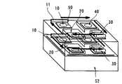
一方、処理ステーションS2は4つのエリアに等分割され、各エリアにコーティング部10、被膜形成部20、洗浄部30および乾燥部40が設けられている。そして処理ステーションS2にはコーティング部10、被膜形成部20、洗浄部30および乾燥部40に順次トレイ50を送り込むとともにトレイ50を払い出す搬送装置60を配置している。
【0019】
搬送装置60によってトレイ50はコーティング部10、被膜形成部20、洗浄部30および乾燥部40間を循環して移動することになる。尚、搬送装置60を処理ステーションS2の周縁部に設置する代わりに各処理部の境界部或いは処理ステーションS2の中心部に搬送装置を設けるようにしてもよい。
【0020】
図4は被膜形成装置の処理ステーションの別実施例を示す図であり、この実施例にあっては処理ステーションを2段構成とし、各段にコーティング部10、被膜形成部20、洗浄部30および乾燥部40を設けている。尚、図示のように上段と下段のトレイ50の移動方向を逆にしてもよい。
【0021】
図5は被膜形成装置の処理ステーションのうち被膜形成部20の別実施例を示す図であり、この実施例にあっては被膜形成部20を多段構成として処理の効率化を図っている。
【0022】
図6に示す別実施例にあっては、乾燥装置4を多段構成とするとともに、各段にホットプレートを設けず全体が加熱装置、つまり壁面にヒータが設けられたオーブン構成としている。このような構成とすることで、基板に上下両面から熱を与えることができ、全体の高さも低くすることができる。
【0023】
また図7(a)に示す乾燥装置4の別実施例にあっては、乾燥装置4を多段構成とするとともに、各段にホットプレートを設けてウェーハ(基板)を乾燥するものである。また、乾燥装置4の上部に排気口が設けられ、排気は、図7(b)に示すように、ヒータの周りの隙間から上方に取られる。さらに、シャッターは各段個別に設けてある。なお、各ホットプレート内に加熱するためのヒータ、熱電対(図示せず)、及び過温センサ(図示せず)を設けている。このような構成とすることで、ピンで浮かせたウェーハに対する昇温スピードを緩やかに上げることができるとともに、乾燥装置の省スペース、高均一性を実現することもできる。
【0024】
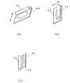
各処理部を循環移動するトレイ50は、図8に示すように、環状をなす外側部材51と、内側部材52とからなる。これら外側部材51と内側部材52はネジ53とキャップボルト54にて厚み方向に位置調整可能とされている。即ち、ネジ53を廻すことで外側部材51と内側部材52との間隔が広がりキャップボルト54を廻すことで間隔が狭まる。
【0025】
内側部材52には内部に通路55が形成され、この通路55は分岐して内側部材52の表面に開口し、通路55の基端部にはカプラ凸部56が取り付けられている。また、図9に示すように、カプラ凸部56は各処理部においてトレイ50を位置決め固定する際に利用され、カプラ凸部56に切替バルブを介して真空源につながるカプラ凹部57を連結することで、基板Wが内側部材52表面に吸着され、カプラ凸部56に切替バルブを介して圧気源につながるカプラ凹部57を連結することで、基板Wを内側部材52表面から持ち上げる際の補助になる。尚、基板Wを内側部材52表面から持ち上げるには、内側部材52に形成した貫通穴58を介してリフトピンで行う。
【0026】
次に、各処理部の詳細について述べる。
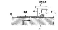
先ず、コーティング部10には図10に示すようにスリットノズル11が往復動可能に配置されている。このスリットノズル11には移動方向を基準として下流側にスキージ12が取り付けられ、スリットノズル11から塗布された塗膜の厚みを均一にならすようにしている。
【0027】
スキージ12はスリットノズル11とは別体としてもよく、またスキージ12の形状としては、図11(a)〜(c)に示すような各種形状が可能である。
スキージ12の形状は上記の他に多くの形状が考えられるが、最初に液面に触れる部分の形状は丸みを帯びている方が液を途切れにくくする。更に最初に液面に触れる箇所をやや膨らませることで、液体を均一化し易く、なお且つスキージの上方に液体が移動するのを防止することができる。
【0028】
図12は被膜形成装置の処理ステーションのうちコーティング部10の別実施例を示す図であり、この実施例にあっては、塗布装置として細長い1つの開口が形成されたスリットノズルを用いずに、幅方向に多数のノズル部13を備えたものを用い、基板Wが半導体ウェーハのような円形の場合には、塗布開始時には中央のノズル部13から塗布液の供給を開始し、塗布装置の移動につれて徐々に外側のノズル部13からも塗布液の供給を行い、また徐々に中央のノズル部からの塗布に戻すようにし、無駄な塗布をなくすようにしている。
【0029】
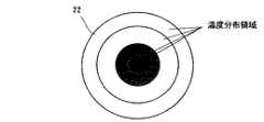
図13は被膜形成装置の処理ステーションS2のうち被膜形成部20の詳細を示す図であり、図14は被膜形成部20のホットプレート22の温度分布を示す平面図である。被膜形成部20には減圧チャンバー21が設置され、この減圧チャンバー21内にホットプレート22が設けられている。尚、以下はホットプレート22を設けた場合について述べる。
【0030】
ホットプレート22は、図14に示すように同心円状に昇温領域が区分けされている。即ち、中央の領域よりも外側の領域の方が昇温速度を遅くしている。尚、昇温速度を異ならせずに中央の領域よりも外側の領域の方が遅くスイッチが入るようにしてもよい。なお、中央の領域も外側の領域も最終の到達温度は約90°である。
【0031】
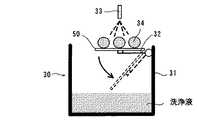
図15は被膜形成装置の処理ステーションS2のうち洗浄部30の断面図であり、洗浄部30には洗浄槽31内にトレイ保持部32が傾動可能に取り付けられ、トレイ保持部32を水平にした状態で、ノズル33から洗浄液をトレイ50上面に供給するとともにテフロン(登録商標)製のブラシ34で洗浄する。洗浄後はトレイ保持部32を斜めにして洗浄液を洗浄槽31内に戻す。洗浄方法としてはトレイ保持部32を傾斜させた状態でブラシ34で洗浄し、或いは洗浄液中に浸漬してもよい。
【0032】
また、図16(a)、及び(b)に示すように、トレイ50を洗浄するにあっては、トレイ保持部32を傾斜させた状態でブラシ34は上下に動き、若しくは左右に動いて洗浄してもよい。更に図16(c)に示すように、ブラシ34と並んで、洗浄液供給ノズル35や乾燥用パージノズル36等を設けて、トレイ保持部32を傾斜させた状態でブラシ34を上下に動かし、若しくは左右に動かして洗浄した後、洗浄液供給ノズルで洗浄液(例えば、蒸留水)を供給してから、乾燥用パージノズルでエアブロー(例えば、窒素)する洗浄方法を用いてもよい。なお、洗浄部の構造としてはトレイ保持部を傾斜させないものでもよく、洗浄液を加熱したり、超音波洗浄を用いることも可能である。
【0033】
以上において、ストックステーションS1のカセット1から未処理基板をハンドリング装置5で取り出し、処理ステーションS2のコーティング部10で待機しているトレイ50の凹部に基板Wをセットする。そして、トレイ50にセットした状態で、スリットノズル11から基板Wの表面に塗布液を供給して塗膜を形成する。このとき、トレイ50のカプラ凸部56は切替バルブを介して真空源につながるカプラ凹部57と連結しており、基板Wはトレイ50に吸着される。
【0034】
この後、トレイ50ごと基板Wを搬送装置60で被膜形成部20に送り込み、基板Wを加熱して表面の塗膜を乾燥させて被膜を形成する。この加熱方法は前記したように中央部が先に高温となるようにする。また、加熱と共にチャンバー21内を減圧しつつ行う。減圧の速度は1分以上かけて10-2Torrとすることで、塗膜内に溶媒が残らないようにする。
【0035】
被膜が形成されたならば、図17(a)に示すようにリフトピンにてトレイ50から基板Wを持ち上げる。このときトレイ50のカプラ凸部56は切替バルブを介して圧気源につながるカプラ凹部57と連結しており、基板Wは圧気源からのエアを補助としてトレイ50からスムーズに持ち上げられる。尚、圧気源からのエアの補助がないと、図17(b)に示すように基板W上と外側部材51上の被膜が切断されにくく基板Wが撓んでしまう。
【0036】
以上の如くして被膜が形成された基板Wをトレイ50から持ち上げたならば、基板WをストックステーションS1のハンドリング装置5で取り上げ、端縁洗浄装置3及び乾燥装置4を経た後、カセット2に処理済基板を収納する。
【0037】
一方、基板Wが払い出されたトレイ50は搬送装置60によって洗浄部30に送り込まれ、前記したブラシと洗浄液により洗浄される。洗浄液はポンプにより廃液タンクに回収された後、蒸留装置にて再生され再び洗浄液として使用する。
【0038】
この後、搬送装置60によって乾燥部40に送り込み、乾燥部40にてトレイ50を乾燥せしめた後、搬送装置60にてトレイ50をコーティング部10に移送する。
【0039】
【発明の効果】
以上に説明したように本発明によれば、トレイに載せたまま基板表面に被膜を形成するにあたり、トレイがコーティング部、被膜形成部、洗浄部および乾燥部を循環移動するようにしたので、効率よく被膜形成を行うことができる。
【0040】
また、被膜形成部において加熱して被膜を形成する際に、基板中央における所定温度までの昇温を外側の昇温よりも遅くしたので、塗膜中の溶媒が一部に残ることなく均一に除去することができる。
【0041】
更に、トレイを2部材から構成して凹部の深さ調整可能とし、更に吸引通路を利用してエアの噴出が可能になるようにしたので、基板の払い出し更には洗浄の際の洗浄液の吸引通路内への侵入防止も図れる。しかも、処理ステーションとストックステーションを隣接させたことで、被膜形成後の基板に対する次工程を速やかに行うことができる。
【図面の簡単な説明】
【図1】 本発明に係る被膜形成装置の全体構成図
【図2】 ハンドリング装置の斜視図
【図3】 ハンドリング装置の平面図
【図4】 被膜形成装置の処理ステーションの別実施例を示す図
【図5】 被膜形成装置の処理ステーションのうち被膜形成部の別実施例を示す図
【図6】 乾燥装置の別実施例を示す図
【図7】 乾燥装置のもう1つの実施例を示す図
【図8】 本発明に係る被膜形成に用いるトレイの断面図
【図9】 トレイのカップリング部の拡大図
【図10】 スリットノズルの側面図
【図11】 (a)〜(c)はスキージの別実施例を示す図
【図12】 被膜形成装置の処理ステーションのうちコーティング部の別実施例を示す図
【図13】 被膜形成装置の処理ステーションのうち被膜形成部の詳細を示す図
【図14】 被膜形成部のホットプレートの温度分布を示す平面図
【図15】 被膜形成装置の処理ステーションのうち洗浄部の断面図
【図16】 図15における洗浄部のブラシの別実施例を示す図
【図17】 (a)はエアの補助で基板をトレイから持ち上げている状態を示す図、(b)はエアの補助なしで基板をトレイから持ち上げている状態を示す図
【符号の説明】
1…未処理基板を収納するカセット、 2…処理済基板を収納するカセット、3…端縁洗浄装置、 4…乾燥装置、 5…ハンドリング装置、 5a,5c,5g、5k…軸、 5b,5d…アーム、 5e…センサ、 5f…支持ブロック、 5h…プレート、 5i、5j…ハンド、 10…コーティング部、 11…スリットノズル、 12…ス
キージ、 13…ノズル部、 20…被膜形成部、 21…減圧チャンバー、 22…ホットプレート、 30…洗浄部、 31…洗浄槽、 32…トレイ保持部、 33…ノズル、 34…ブラシ、 35…洗浄液供給ノズル、 36…乾燥用パージノズル、 40…乾燥部、 50…トレイ、 51…外側部材、 52…内側部材、 53…ネジ、 54…キャップボルト、 55…通路、 56…カプラ凸部、 57…カプラ凹部、 58…貫通穴、 60…搬送装置、 S1…ストックステーション、 S2…処理ステーション、 W…ウェーハ。[0001]
BACKGROUND OF THE INVENTION
The present invention relates to a tray suitable for use ina process of forminga film, for example, a thick film of 20 μm or more on the surface of a substrate such as a glass substrate or a semiconductor wafer.
[0002]
[Prior art]
As a method for forming a resist film or an SOG film on the surface of a substrate such as a glass substrate or a semiconductor wafer, there are a spin coating method and a slit nozzle method.
The spin coating method is a method in which a plate-like object is rotated at a high speed with a spinner, and a coating solution dropped on the center of the plate-like object is diffused by centrifugal force. Yes. In particular, in this prior art, a concave portion into which a plate-like workpiece is fitted is formed on the upper surface of the spinner head.
Further, the slit nozzle method is disclosed in US Pat. No. 4,696,885 and the like, and the coating liquid is applied from the slit nozzle having the same width as the plate-like object to be processed to the plate-like object. In this method, a coating film is formed in a predetermined range by being moved relatively while dropping in a curtain shape.
[0003]
Recently, however, attempts have been made to form a thick film on the substrate surface. For example, in order to form a protruding electrode having a height of about 20 μm called a bump on the IC pattern surface by applying an integrated circuit forming technique, it is necessary to form a resist film having a thickness of about 20 μm.
Conventionally, wire bonding is performed to mount an IC chip on a substrate. However, in wire bonding, gold wires must be connected one by one, which is troublesome and takes time. Therefore, instead of wire bonding, a plurality of metal columns are provided on the chip itself, and the IC chip is mounted on the substrate via the metal columns. The height of the metal pillar is about 100 μm, and it is necessary to form a resist film having a thickness of about 100 μm in order to form the metal pillar by applying the integrated circuit forming technique.
[0004]
[Problems to be solved by the invention]
In the spin coating method, the amount of the coating solution involved in film formation is as small as about 5% of the supplied coating solution, and most of it is scattered by centrifugal force. There is also a problem that a thick film cannot be obtained.
Furthermore, the dimension of the substrate (glass substrate) becomes larger and the thickness tends to become thinner, and the substrate is bent by its own weight when the substrate is transported.
[0005]
On the other hand, according to the slit nozzle method, waste of the coating liquid can be reduced and the film thickness can be increased. However, in the slit nozzle method, there is a problem that the film thickness at the application start position and the application end position becomes extremely thick as compared with other parts due to the influence of the surface tension.
[0006]
The above-mentioned prior arts all relate to the application of the coating liquid, and after applying the coating liquid, the film is dried by heating to form a coating, and the subsequent processes can be efficiently processed. is not.
[0007]
In particular, when a thick film is formed, a problem peculiar to the conventional apparatus arises in recent years when the substrate size is increased.
That is, when the coating film applied on the substrate is heated and dried, the surface of the coating film is dried and cured before the inside of the coating film. The residual ratio of the solvent differs for each part of the film, and as a result, the high aspect ratio pattern peels off from the substrate surface after development, or wrinkles occur in the coating film.
In addition, if each process is carried while the substrate is placed on the tray, the substrate can be prevented from bending, but when a thick film is formed on the substrate surface when the substrate is lifted from the tray, the weight is added. There is a possibility that the substrate is bent and damaged.
[0008]
[Means for Solving the Problems]
In order to solve each of the above problems, thetray used for both transporting and processing thesubstrate according to
[0013]
DETAILED DESCRIPTION OF THE INVENTION
Embodiments of the present invention will be described below with reference to the accompanying drawings. FIG. 1 is an overall configuration diagram of a film forming apparatus according to the present invention. The film forming apparatus has a substrate stock station S1 and a processing station S2 adjacent to each other, and a
[0014]
As shown in FIG. 2, the
[0015]
The hands 5i and 5j are 90 ° different from each other, and the front and rear positions of the hands 5i and 5j are switched by rotating the
By rotating h by 180 ° around the
[0016]
The wafer (substrate)
Conventionally, the
[0017]
Further, the processed wafer (substrate) is stored in the cassette by the reverse operation. Here, since the processed wafer is heated, the hand holding the wafer is also heated. When an unprocessed substrate is held with a high-temperature hand, the temperature distribution of the unprocessed substrate becomes non-uniform. Therefore, if a hand for holding an unprocessed substrate and a hand for holding a processed substrate are determined in advance as described above, such disadvantages can be prevented.
[0018]
On the other hand, the processing station S2 is equally divided into four areas, and a
[0019]
The
[0020]
FIG. 4 is a diagram showing another embodiment of the processing station of the film forming apparatus. In this embodiment, the processing station has a two-stage configuration, and each stage includes a
[0021]
FIG. 5 is a diagram showing another embodiment of the coating
[0022]
In another embodiment shown in FIG. 6, the drying
[0023]
Further, in another embodiment of the
[0024]
As shown in FIG. 8, the
[0025]
A
[0026]
Next, details of each processing unit will be described.
First, as shown in FIG. 10, a
[0027]
The
There are many other shapes for the
[0028]
FIG. 12 is a view showing another embodiment of the
[0029]
FIG. 13 is a diagram showing details of the
[0030]
As shown in FIG. 14, the
[0031]
FIG. 15 is a cross-sectional view of the
[0032]
Also, as shown in FIGS. 16A and 16B, when cleaning the
[0033]
In the above, the unprocessed substrate is taken out from the
[0034]
After that, the substrate W together with the
[0035]
When the film is formed, the substrate W is lifted from the
[0036]
When the substrate W with the coating formed thereon is lifted from the
[0037]
On the other hand, the
[0038]
Thereafter, the sheet is fed into the drying
[0039]
【The invention's effect】
As described above, according to the present invention, when the film is formed on the surface of the substrate while being placed on the tray, the tray circulates and moves through the coating part, the film forming part, the cleaning part, and the drying part. The film can be formed well.
[0040]
In addition, when forming a film by heating in the film forming part, the temperature rise to a predetermined temperature in the center of the substrate is slower than the temperature rise outside, so that the solvent in the film remains uniform without remaining in part. Can be removed.
[0041]
Further, the tray is composed of two members so that the depth of the concave portion can be adjusted, and air can be blown out by using the suction passage, so that the suction passage for the cleaning liquid when the substrate is discharged and the cleaning is performed. You can also prevent intrusion. In addition, since the processing station and the stock station are adjacent to each other, the next process for the substrate after the film formation can be performed quickly.
[Brief description of the drawings]
FIG. 1 is an overall configuration diagram of a film forming apparatus according to the present invention. FIG. 2 is a perspective view of a handling apparatus. FIG. 3 is a plan view of a handling apparatus. FIG. 5 is a view showing another embodiment of the film forming unit in the processing station of the film forming apparatus. FIG. 6 is a view showing another embodiment of the drying apparatus. FIG. 7 is a view showing another embodiment of the drying apparatus. 8 is a cross-sectional view of a tray used for film formation according to the present invention. FIG. 9 is an enlarged view of a coupling portion of the tray. FIG. 10 is a side view of a slit nozzle. FIG. 12 is a diagram showing another embodiment of the coating unit in the processing station of the film forming apparatus. FIG. 13 is a diagram showing details of the film forming unit in the processing station of the film forming apparatus. 14) Film formation part FIG. 15 is a cross-sectional view of the cleaning unit in the processing station of the film forming apparatus. FIG. 16 is a diagram illustrating another embodiment of the brush of the cleaning unit in FIG. ) Is a diagram showing a state where the substrate is lifted from the tray with the assistance of air, and (b) is a diagram showing a state where the substrate is being lifted from the tray without the assistance of air.
DESCRIPTION OF
Claims (3)
Translated fromJapanesePriority Applications (4)
| Application Number | Priority Date | Filing Date | Title |
|---|---|---|---|
| JP2002346230AJP4118659B2 (en) | 2001-12-03 | 2002-11-28 | Substrate tray |
| KR1020020076147AKR20030045636A (en) | 2001-12-03 | 2002-12-03 | Apparatus and method for forming a coating film, and tray for a substrate |
| TW091135075ATWI249435B (en) | 2001-12-03 | 2002-12-03 | Coating film forming device, coating film forming method and wafer tray |
| US10/308,964US7005009B2 (en) | 2001-12-03 | 2002-12-03 | Film forming apparatus, film forming method and tray for substrate |
Applications Claiming Priority (3)
| Application Number | Priority Date | Filing Date | Title |
|---|---|---|---|
| JP2001-369243 | 2001-12-03 | ||
| JP2001369243 | 2001-12-03 | ||
| JP2002346230AJP4118659B2 (en) | 2001-12-03 | 2002-11-28 | Substrate tray |
Related Child Applications (1)
| Application Number | Title | Priority Date | Filing Date |
|---|---|---|---|
| JP2006115338ADivisionJP2006208005A (en) | 2001-12-03 | 2006-04-19 | Drier |
Publications (2)
| Publication Number | Publication Date |
|---|---|
| JP2003245591A JP2003245591A (en) | 2003-09-02 |
| JP4118659B2true JP4118659B2 (en) | 2008-07-16 |
Family
ID=26624853
Family Applications (1)
| Application Number | Title | Priority Date | Filing Date |
|---|---|---|---|
| JP2002346230AExpired - Fee RelatedJP4118659B2 (en) | 2001-12-03 | 2002-11-28 | Substrate tray |
Country Status (4)
| Country | Link |
|---|---|
| US (1) | US7005009B2 (en) |
| JP (1) | JP4118659B2 (en) |
| KR (1) | KR20030045636A (en) |
| TW (1) | TWI249435B (en) |
Families Citing this family (32)
| Publication number | Priority date | Publication date | Assignee | Title |
|---|---|---|---|---|
| JP2005161168A (en)* | 2003-12-01 | 2005-06-23 | Tokyo Ohka Kogyo Co Ltd | Film forming method |
| JP4443393B2 (en) | 2004-11-29 | 2010-03-31 | 東京応化工業株式会社 | Coating apparatus, coating method, and film forming apparatus |
| KR100780718B1 (en) | 2004-12-28 | 2007-12-26 | 엘지.필립스 엘시디 주식회사 | Slit coater with coating liquid supply device |
| KR100700180B1 (en) | 2004-12-31 | 2007-03-27 | 엘지.필립스 엘시디 주식회사 | Slit coater with preliminary discharge and coating method using the same |
| KR100675643B1 (en) | 2004-12-31 | 2007-02-02 | 엘지.필립스 엘시디 주식회사 | Slit Coater |
| KR100700181B1 (en) | 2004-12-31 | 2007-03-27 | 엘지.필립스 엘시디 주식회사 | Slit coater with nozzle waiting portion and coating method using the same |
| US8118535B2 (en)* | 2005-05-18 | 2012-02-21 | International Business Machines Corporation | Pod swapping internal to tool run time |
| US8063318B2 (en)* | 2007-09-25 | 2011-11-22 | Silverbrook Research Pty Ltd | Electronic component with wire bonds in low modulus fill encapsulant |
| US7659141B2 (en)* | 2007-09-25 | 2010-02-09 | Silverbrook Research Pty Ltd | Wire bond encapsulant application control |
| US7741720B2 (en)* | 2007-09-25 | 2010-06-22 | Silverbrook Research Pty Ltd | Electronic device with wire bonds adhered between integrated circuits dies and printed circuit boards |
| CN102441510B (en)* | 2010-10-11 | 2013-10-02 | 海洋王照明科技股份有限公司 | Dipping, pulling and film-forming device |
| US9221081B1 (en) | 2011-08-01 | 2015-12-29 | Novellus Systems, Inc. | Automated cleaning of wafer plating assembly |
| US9988734B2 (en) | 2011-08-15 | 2018-06-05 | Lam Research Corporation | Lipseals and contact elements for semiconductor electroplating apparatuses |
| US9228270B2 (en) | 2011-08-15 | 2016-01-05 | Novellus Systems, Inc. | Lipseals and contact elements for semiconductor electroplating apparatuses |
| US10066311B2 (en) | 2011-08-15 | 2018-09-04 | Lam Research Corporation | Multi-contact lipseals and associated electroplating methods |
| WO2013148890A1 (en)* | 2012-03-28 | 2013-10-03 | Novellus Systems, Inc. | Methods and apparatuses for cleaning electroplating substrate holders |
| US9476139B2 (en) | 2012-03-30 | 2016-10-25 | Novellus Systems, Inc. | Cleaning electroplating substrate holders using reverse current deplating |
| KR101941998B1 (en)* | 2012-04-03 | 2019-01-25 | 삼성디스플레이 주식회사 | Apparatus for coating and a method for coating using the same |
| CN102641820A (en)* | 2012-04-25 | 2012-08-22 | 深圳市科聚新材料有限公司 | Speed and angle adjustable dip-coating film forming device |
| US10416092B2 (en) | 2013-02-15 | 2019-09-17 | Lam Research Corporation | Remote detection of plating on wafer holding apparatus |
| US9746427B2 (en) | 2013-02-15 | 2017-08-29 | Novellus Systems, Inc. | Detection of plating on wafer holding apparatus |
| KR101858246B1 (en)* | 2014-11-06 | 2018-05-16 | 가부시키가이샤 에나테크 | Coating apparatus, coating head, and coating method |
| US10053793B2 (en) | 2015-07-09 | 2018-08-21 | Lam Research Corporation | Integrated elastomeric lipseal and cup bottom for reducing wafer sticking |
| JP6782628B2 (en)* | 2016-12-21 | 2020-11-11 | 東京エレクトロン株式会社 | Substrate processing equipment, substrate processing system and substrate processing method |
| CN111448849A (en) | 2017-11-10 | 2020-07-24 | 诺信公司 | System and method for coating a substrate |
| JP7079044B2 (en)* | 2019-05-31 | 2022-06-01 | 株式会社九州日昌 | Heating device and heating method |
| WO2020241489A1 (en)* | 2019-05-31 | 2020-12-03 | 株式会社九州日昌 | Heating device and heating method |
| JP7079042B2 (en)* | 2019-05-31 | 2022-06-01 | 株式会社九州日昌 | Heating device and heating method |
| CN112174543A (en)* | 2019-07-03 | 2021-01-05 | 北京铂阳顶荣光伏科技有限公司 | Chemical bath coating equipment and chemical bath coating system |
| CN114450439A (en)* | 2019-10-03 | 2022-05-06 | 洛佩诗公司 | Processing device and epitaxial reactor with storage chamber |
| CN113617231B (en)* | 2021-07-14 | 2023-11-17 | 上海海洋大学 | Flat membrane preparation device |
| CN118689038B (en)* | 2024-08-26 | 2025-01-28 | 西北工业大学 | Manufacturing method of large-scale and high-depth micro-nanostructures |
Family Cites Families (4)
| Publication number | Priority date | Publication date | Assignee | Title |
|---|---|---|---|---|
| US4418639A (en)* | 1981-05-19 | 1983-12-06 | Solitec, Inc. | Apparatus for treating semiconductor wafers |
| KR970007060B1 (en)* | 1989-02-17 | 1997-05-02 | 다이닛뽕 인사쓰 가부시끼가이샤 | Coating method and coating device for viscous liquid |
| JPH04361871A (en)* | 1991-06-06 | 1992-12-15 | Pioneer Electron Corp | Dispenser for applying cream solder |
| US6395335B2 (en)* | 1996-12-10 | 2002-05-28 | Matsushita Electric Industrial Co., Ltd. | Apparatus and method for printing solder paste |
- 2002
- 2002-11-28JPJP2002346230Apatent/JP4118659B2/ennot_activeExpired - Fee Related
- 2002-12-03USUS10/308,964patent/US7005009B2/ennot_activeExpired - Lifetime
- 2002-12-03KRKR1020020076147Apatent/KR20030045636A/ennot_activeWithdrawn
- 2002-12-03TWTW091135075Apatent/TWI249435B/enactive
Also Published As
| Publication number | Publication date |
|---|---|
| TW200301163A (en) | 2003-07-01 |
| US7005009B2 (en) | 2006-02-28 |
| TWI249435B (en) | 2006-02-21 |
| US20030134044A1 (en) | 2003-07-17 |
| KR20030045636A (en) | 2003-06-11 |
| JP2003245591A (en) | 2003-09-02 |
Similar Documents
| Publication | Publication Date | Title |
|---|---|---|
| JP4118659B2 (en) | Substrate tray | |
| JP5058085B2 (en) | Substrate cleaning device | |
| TWI567815B (en) | Substrate cleaning method, substrate cleaning apparatus and storage medium for cleaning substrate | |
| US6332723B1 (en) | Substrate processing apparatus and method | |
| TWI636158B (en) | Substrate processing method and substrate processing device | |
| TWI775574B (en) | Substrate processing method and substrate processing apparatus | |
| JP5726686B2 (en) | Liquid processing apparatus and method for controlling liquid processing apparatus | |
| JP4343050B2 (en) | Development processing apparatus and method thereof | |
| JP2004207573A (en) | Coating processor | |
| CN111063633B (en) | Substrate processing device and substrate processing method | |
| CN1582489A (en) | Substrate treating device and substrate treating method | |
| CN114695185A (en) | Substrate processing apparatus and substrate processing method | |
| JP2001232250A (en) | Membrane forming apparatus | |
| JP2007103956A (en) | Substrate treatment device | |
| JP3958572B2 (en) | Substrate processing apparatus and substrate processing method | |
| KR100672942B1 (en) | Substrate drying apparatus and method used for semiconductor device manufacturing | |
| JP2017118049A (en) | Substrate processing apparatus, substrate processing method and storage medium | |
| JP7232710B2 (en) | Substrate processing method and substrate processing apparatus | |
| JP3909574B2 (en) | Resist coating device | |
| KR20220031499A (en) | Liquid treatment method and liquid treatment apparatus | |
| JP2006208005A (en) | Drier | |
| JP3822745B2 (en) | Cleaning device | |
| JP5970102B2 (en) | Liquid processing equipment | |
| WO2004036633A1 (en) | Liquid processing device | |
| KR20090065796A (en) | Substrate Processing Apparatus and Method |
Legal Events
| Date | Code | Title | Description |
|---|---|---|---|
| A621 | Written request for application examination | Free format text:JAPANESE INTERMEDIATE CODE: A621 Effective date:20050413 | |
| A977 | Report on retrieval | Free format text:JAPANESE INTERMEDIATE CODE: A971007 Effective date:20070405 | |
| A131 | Notification of reasons for refusal | Free format text:JAPANESE INTERMEDIATE CODE: A131 Effective date:20071023 | |
| A521 | Request for written amendment filed | Free format text:JAPANESE INTERMEDIATE CODE: A523 Effective date:20071218 | |
| A131 | Notification of reasons for refusal | Free format text:JAPANESE INTERMEDIATE CODE: A131 Effective date:20080129 | |
| A521 | Request for written amendment filed | Free format text:JAPANESE INTERMEDIATE CODE: A523 Effective date:20080328 | |
| TRDD | Decision of grant or rejection written | ||
| A01 | Written decision to grant a patent or to grant a registration (utility model) | Free format text:JAPANESE INTERMEDIATE CODE: A01 Effective date:20080422 | |
| A61 | First payment of annual fees (during grant procedure) | Free format text:JAPANESE INTERMEDIATE CODE: A61 Effective date:20080423 | |
| R150 | Certificate of patent or registration of utility model | Free format text:JAPANESE INTERMEDIATE CODE: R150 Ref document number:4118659 Country of ref document:JP Free format text:JAPANESE INTERMEDIATE CODE: R150 | |
| FPAY | Renewal fee payment (event date is renewal date of database) | Free format text:PAYMENT UNTIL: 20110502 Year of fee payment:3 | |
| FPAY | Renewal fee payment (event date is renewal date of database) | Free format text:PAYMENT UNTIL: 20110502 Year of fee payment:3 | |
| FPAY | Renewal fee payment (event date is renewal date of database) | Free format text:PAYMENT UNTIL: 20120502 Year of fee payment:4 | |
| R250 | Receipt of annual fees | Free format text:JAPANESE INTERMEDIATE CODE: R250 | |
| FPAY | Renewal fee payment (event date is renewal date of database) | Free format text:PAYMENT UNTIL: 20130502 Year of fee payment:5 | |
| R250 | Receipt of annual fees | Free format text:JAPANESE INTERMEDIATE CODE: R250 | |
| FPAY | Renewal fee payment (event date is renewal date of database) | Free format text:PAYMENT UNTIL: 20140502 Year of fee payment:6 | |
| R250 | Receipt of annual fees | Free format text:JAPANESE INTERMEDIATE CODE: R250 | |
| R250 | Receipt of annual fees | Free format text:JAPANESE INTERMEDIATE CODE: R250 | |
| R250 | Receipt of annual fees | Free format text:JAPANESE INTERMEDIATE CODE: R250 | |
| R250 | Receipt of annual fees | Free format text:JAPANESE INTERMEDIATE CODE: R250 | |
| R250 | Receipt of annual fees | Free format text:JAPANESE INTERMEDIATE CODE: R250 | |
| R250 | Receipt of annual fees | Free format text:JAPANESE INTERMEDIATE CODE: R250 | |
| R250 | Receipt of annual fees | Free format text:JAPANESE INTERMEDIATE CODE: R250 | |
| R250 | Receipt of annual fees | Free format text:JAPANESE INTERMEDIATE CODE: R250 | |
| R250 | Receipt of annual fees | Free format text:JAPANESE INTERMEDIATE CODE: R250 | |
| LAPS | Cancellation because of no payment of annual fees |