JP4118187B2 - Manufacturing method of solar cell - Google Patents
Manufacturing method of solar cellDownload PDFInfo
- Publication number
- JP4118187B2 JP4118187B2JP2003131797AJP2003131797AJP4118187B2JP 4118187 B2JP4118187 B2JP 4118187B2JP 2003131797 AJP2003131797 AJP 2003131797AJP 2003131797 AJP2003131797 AJP 2003131797AJP 4118187 B2JP4118187 B2JP 4118187B2
- Authority
- JP
- Japan
- Prior art keywords
- solar cell
- insulating film
- gas
- film
- substrate
- Prior art date
- Legal status (The legal status is an assumption and is not a legal conclusion. Google has not performed a legal analysis and makes no representation as to the accuracy of the status listed.)
- Expired - Fee Related
Links
Images


Classifications
- H—ELECTRICITY
- H10—SEMICONDUCTOR DEVICES; ELECTRIC SOLID-STATE DEVICES NOT OTHERWISE PROVIDED FOR
- H10F—INORGANIC SEMICONDUCTOR DEVICES SENSITIVE TO INFRARED RADIATION, LIGHT, ELECTROMAGNETIC RADIATION OF SHORTER WAVELENGTH OR CORPUSCULAR RADIATION
- H10F10/00—Individual photovoltaic cells, e.g. solar cells
- H10F10/10—Individual photovoltaic cells, e.g. solar cells having potential barriers
- H10F10/14—Photovoltaic cells having only PN homojunction potential barriers
- H10F10/146—Back-junction photovoltaic cells, e.g. having interdigitated base-emitter regions on the back side
- H—ELECTRICITY
- H10—SEMICONDUCTOR DEVICES; ELECTRIC SOLID-STATE DEVICES NOT OTHERWISE PROVIDED FOR
- H10F—INORGANIC SEMICONDUCTOR DEVICES SENSITIVE TO INFRARED RADIATION, LIGHT, ELECTROMAGNETIC RADIATION OF SHORTER WAVELENGTH OR CORPUSCULAR RADIATION
- H10F10/00—Individual photovoltaic cells, e.g. solar cells
- H10F10/10—Individual photovoltaic cells, e.g. solar cells having potential barriers
- H10F10/14—Photovoltaic cells having only PN homojunction potential barriers
- H—ELECTRICITY
- H10—SEMICONDUCTOR DEVICES; ELECTRIC SOLID-STATE DEVICES NOT OTHERWISE PROVIDED FOR
- H10F—INORGANIC SEMICONDUCTOR DEVICES SENSITIVE TO INFRARED RADIATION, LIGHT, ELECTROMAGNETIC RADIATION OF SHORTER WAVELENGTH OR CORPUSCULAR RADIATION
- H10F71/00—Manufacture or treatment of devices covered by this subclass
- H10F71/121—The active layers comprising only Group IV materials
- H—ELECTRICITY
- H10—SEMICONDUCTOR DEVICES; ELECTRIC SOLID-STATE DEVICES NOT OTHERWISE PROVIDED FOR
- H10F—INORGANIC SEMICONDUCTOR DEVICES SENSITIVE TO INFRARED RADIATION, LIGHT, ELECTROMAGNETIC RADIATION OF SHORTER WAVELENGTH OR CORPUSCULAR RADIATION
- H10F71/00—Manufacture or treatment of devices covered by this subclass
- H10F71/129—Passivating
- H—ELECTRICITY
- H10—SEMICONDUCTOR DEVICES; ELECTRIC SOLID-STATE DEVICES NOT OTHERWISE PROVIDED FOR
- H10F—INORGANIC SEMICONDUCTOR DEVICES SENSITIVE TO INFRARED RADIATION, LIGHT, ELECTROMAGNETIC RADIATION OF SHORTER WAVELENGTH OR CORPUSCULAR RADIATION
- H10F77/00—Constructional details of devices covered by this subclass
- H10F77/30—Coatings
- H10F77/306—Coatings for devices having potential barriers
- H10F77/311—Coatings for devices having potential barriers for photovoltaic cells
- Y—GENERAL TAGGING OF NEW TECHNOLOGICAL DEVELOPMENTS; GENERAL TAGGING OF CROSS-SECTIONAL TECHNOLOGIES SPANNING OVER SEVERAL SECTIONS OF THE IPC; TECHNICAL SUBJECTS COVERED BY FORMER USPC CROSS-REFERENCE ART COLLECTIONS [XRACs] AND DIGESTS
- Y02—TECHNOLOGIES OR APPLICATIONS FOR MITIGATION OR ADAPTATION AGAINST CLIMATE CHANGE
- Y02E—REDUCTION OF GREENHOUSE GAS [GHG] EMISSIONS, RELATED TO ENERGY GENERATION, TRANSMISSION OR DISTRIBUTION
- Y02E10/00—Energy generation through renewable energy sources
- Y02E10/50—Photovoltaic [PV] energy
- Y02E10/547—Monocrystalline silicon PV cells
- Y—GENERAL TAGGING OF NEW TECHNOLOGICAL DEVELOPMENTS; GENERAL TAGGING OF CROSS-SECTIONAL TECHNOLOGIES SPANNING OVER SEVERAL SECTIONS OF THE IPC; TECHNICAL SUBJECTS COVERED BY FORMER USPC CROSS-REFERENCE ART COLLECTIONS [XRACs] AND DIGESTS
- Y02—TECHNOLOGIES OR APPLICATIONS FOR MITIGATION OR ADAPTATION AGAINST CLIMATE CHANGE
- Y02P—CLIMATE CHANGE MITIGATION TECHNOLOGIES IN THE PRODUCTION OR PROCESSING OF GOODS
- Y02P70/00—Climate change mitigation technologies in the production process for final industrial or consumer products
- Y02P70/50—Manufacturing or production processes characterised by the final manufactured product
Landscapes
- Chemical Vapour Deposition (AREA)
- Photovoltaic Devices (AREA)
- Formation Of Insulating Films (AREA)
Description
Translated fromJapanese【0001】
【発明の属する技術分野】
この発明は、光エネルギーを直接電気エネルギーに変換する太陽電池とその製造方法に関する。
【0002】
【従来の技術】
【特許文献1】
特開平10−83988号公報
【特許文献2】
特開平8−250438号公報
【0003】
太陽電池は、光エネルギーを電力に変換する半導体素子であり、p−n接合型、pin型、ショットキー型などがあり、特にp−n接合型が広く用いられている。また、太陽電池をその基板材料をもとに分類すると、シリコン結晶系太陽電池、アモルファス(非晶質)シリコン系太陽電池、化合物半導体系太陽電池の3種類に大きく分けられる。シリコン結晶系太陽電池は、さらに、単結晶系太陽電池と多結晶系太陽電池に分類される。太陽電池用シリコン結晶基板は比較的容易に製造できることから、シリコン結晶系太陽電池が最も普及している。
【0004】
上記のごとき太陽電池の出力特性は、一般に、ソーラーシミュレータを用いて出力電流電圧曲線を測定することにより評価される。この曲線上で、出力電流Ipと出力電圧Vpとの積Ip・Vpが最大となる点Pmを最大出力Pmと呼び、該Pmを太陽電池に入射する総光エネルギー(S×I:Sは素子面積、Iは照射する光の強度)にて除した値:
η≡{Pm/(S×I)}×100 (%) ‥‥(1)
が太陽電池の変換効率ηとして定義される。変換効率ηを高めるには、短絡電流Isc(電流電圧曲線上にてV=0のときの出力電流値)あるいは開放電圧Voc(同じくI=0のときの出力電圧値)を大きくすること、及び、出力電流電圧曲線をなるべく角型に近い形状のものとすることが重要である。なお、出力電流電圧曲線の角型の度合いは、一般に、
FF≡Ipm×Vpm/(Isc×Voc) ‥‥(2)
にて定義されるフィルファクタ(曲線因子)により評価でき、該FFの値が1に近いほど出力電流電圧曲線が理想的な角型に近づき、変換効率ηも高められることを意味する。
【0005】
上記変換効率ηを向上させるには、キャリア(電子とホール)の表面再結合を低減させることが重要である。具体的に説明すれば、単結晶シリコン又は多結晶シリコンなどを基板として用いた太陽電池においては、太陽光などの入射光によって光生成した少数キャリアが、主に拡散によってp−n接合面へ到達した後、受光面及び裏面に取り付けられた電極から多数キャリアとして外部へ取り出され、電気エネルギーとなる。その際、電極面以外の基板表面に存在する界面準位を介して、本来電流として取り出すことのできたキャリアが再結合して失われることがあり、変換効率ηの低下につながる。
【0006】
そこで、高効率太陽電池においては、半導体基板の受光面と裏面とを、電極とのコンタクト部を除いて絶縁膜で保護し、半導体基板と各絶縁膜との界面におけるキャリア再結合を抑制し、変換効率ηの向上が図られている(いわゆる表面パッシペーション効果)。このような絶縁膜としては、酸化珪素膜が古くから使われているが、屈折率が1.4程度と低く、受光面側に用いた場合の反射損失がやや大きいため、近年では、より高屈折率の窒化珪素が、パッシペーション効果だけでなく反射防止効果にも優れていることから、広く用いられるようになってきている。窒化珪素膜は、従来、熱CVD、プラズマCVDあるいは光CVDなどのCVD法(Chemical Vapor Deposition:化学気相堆積法)によって形成される。この中で、最も一般的に普及しているのはプラズマCVDである。
【0007】
図3は、一般にダイレクトプラズマCVDと呼ばれる、バッチ式平行平板プラズマCVD装置を模式的に示すものである。該装置は、排気装置11を備えた反応容器1、反応容器1内の所定位置に太陽電池基板20を配置するための基板ホルダ81、反応性ガスである所定の成膜用ガスを反応容器1内に導入する成膜用ガス導入路31,32、導入されたガスにエネルギーを与えてプラズマを発生させる高周波電源82、及び、堆積雰囲気を一定温度に保つための抵抗熱加熱式ヒーター90を有する。該装置を用いて薄膜を堆積する場合、成膜用ガス導入路31,32によって所定の成膜用ガスを所定の流量で反応容器1内に導入した後、高周波電源82を動作させて高周波電界を設定する。この操作により、基板ホルダ81間で高周波放電が発生して成膜用ガスがプラズマ化し、該プラズマによって生ずる反応を利用して、基板20の表面に得るべき絶縁膜が作製される。例えば、絶縁膜としてシリコン窒化膜を作製する場合には、成膜用ガスとしてシランを成膜用ガス導入路31から、アンモニアを成膜用ガス導入路32から導入・、混合後、反応容器1に供給し、プラズマ中でのシランの分解反応等を利用してシリコン窒化膜を生成させる。
【0008】
【発明が解決しようとする課題】
プラズマCVDは、基板温度が400℃以下の低温であっても比較的高い堆積速度を有するため、太陽電池用の製造プロセスに多用されている。しかしながら、プラズマ中で生成される高エネルギー荷電粒子が、堆積した膜や基板表面に損傷(いわゆるプラズマダメージ)を与えやすいため、得られる窒化珪素膜は界面準位密度が多くなり、十分なパッシベーション効果が得られない問題がある。また、太陽電池の諸特性にも影響が及びやすい。
【0009】
そこで、プラズマダメージを抑制した方法として、ECR(電子サイクロトロン共鳴)プラズマを利用したCVD法が提案されている。図4は、その装置の一例を模式的に示すものである。該方法は、従来のプラズマCVDとは異なり、ラジカル種を分離して利用するために、処理すべき基板表面をプラズマ領域(プラズマゾーン)から離れた位置に配置する点に特徴があり、以下、リモートプラズマCVDと称する。具体的には、成膜用ガス導入路31によって所定の成膜用ガスを所定の流量で前室101内に導入した後、マイクロ波発生装置102を用いて、高周波電界の代わりにマイクロ波を前室101に印加する。このマイクロ波によって、キャリアガス兼成膜用ガスがプラズマ化し、反応活性種が発生する。該反応活性種は処理容器内1に流れこみ、成膜用ガス導入路32より供給された別の成膜用ガスと化学反応を起こすことにより、基板20の表面に絶縁膜が形成される。絶縁膜として窒化珪素膜を作製する場合は、キャリアガス兼成膜用ガスとして導入路31にアンモニアを、導入路32にシランをそれぞれ導入して混合し、プラズマ中によるアンモニアの分解反応等を利用して窒化珪素膜を生成する。上記リモートプラズマCVDを用いるとプラズマダメージを多少は軽減できる。
【0010】
しかし、いずれにしてもプラズマCVDを用いる限り、プラズマダメージが大きいことに変わりはなく、膜中のダングリングボンドの形成も顕著となるから、パッシベーション効果の向上には、多量の水素を膜中に含有させてダングリングボンドの封止を図る必要があった(また、周知のプラズマCVDでは、原料ガス由来の水素が必然的に多量に取り込まれてしまう背景もある)。その結果、得られる窒化珪素膜は最大で40atom%もの水素原子を含有しており、太陽光など紫外線を多く含む光の照射を受け続けると、パッシベーション効果が経時的に劣化する問題がある。
【0011】
また、プラズマCVDによる窒化珪素膜では、いわゆるフィールド効果パッシベーションを得るために、膜組成を化学量論比から珪素過剰側に相当大きくシフトさせていた。すなわち、膜組成が珪素過剰側に大きく外れると、アニオン欠損により生ずる電子が半導体基板側に流出して、カチオン側の正電荷が固定電荷を形成するため、バンドベンディングが生じる。すると、接触界面の近傍にて半導体基板側に電子が過剰となる反転層が形成されるので、これを利用してパッシベーション効果を高めることができる。
【0012】
しかし、この構造には次のごとく、大きな欠点がある。
▲1▼裏面電極として使用する場合、図5に示すように、p型基板111の電極64近傍に形成された反転層112が、電極面内での短絡113を引き起こしやすく、生成電流の低下につながる。
▲2▼電子流出による反転層形成により、フィールド効果パッシベーションが顕著となるのは基板のp型層側に適用した場合のみである。太陽電池において、基板のp型領域及びn型領域に光励起により生成するキャリアは少数キャリアであり、光吸収に寄与する基板の要部は、ライフタイムの長い電子が少数キャリアとなるp型の基板を使用することが有利であるが、この場合は、n型エミッタ層が形成される受光面側には十分なパッシベーション効果を発揮できなくなる。また、エミッタ層表面はドーパント濃度が高すぎるため、窒化珪素膜中の固定電荷程度ではバンドベンディングがほとんど起こらず、前述のフィールド効果パッシベーションは期待するべくもない。従って、エミッタ層においては、プラズマダメージの抑制、ひいてはそれによる界面準位抑制が、良好なパッシベーション特性の鍵を握ることになる。しかし、通常のプラズマCVDではダメージ抑制は難しいから、結局のところ良好なパッシベーション効果は得られない。
【0013】
本発明は、パッシベーション効果に優れ、また、パッシベーション効果の経時劣化を生じにくい絶縁膜を有した太陽電池と、その製造方法とを提供することにある。
【0014】
【課題を解決するための手段及び作用・効果】
上記の課題を解決するため、本発明の太陽電池の第一は、第一主表面に受光面が形成されるとともに、該受光面に照射される光に基づいて光起電力を発生させる半導体太陽電池基板を備え、該半導体太陽電池基板の受光面が、カチオン成分の主体が珪素である無機絶縁材料(以下、珪素系絶縁材料ともいう)からなる無機絶縁膜としての受光面側絶縁膜にて被覆され、該受光面側絶縁膜を、水素含有率が10原子%未満の低水素含有無機絶縁膜として構成したことを特徴とする。なお、本明細書において「カチオン成分の主体が珪素である」とは、無機絶縁材料のカチオン成分の50%以上(望ましくは80%以上)が珪素であることを意味する。なお、以下に説明する本発明の効果が達成される限り、材料の絶縁性が過度に損なわれない範囲で、珪素以外のカチオンが含有されていてもよい。例えば、セシウムカチオンなどイオン半径の大きいアルカリ金属イオンを窒化膜中に導入し、膜中の固定電荷を増大して、フィールド効果パッシベーションの寄与を図る、といったことも可能である。
【0015】
上記本発明の太陽電池の第一によると、受光面側絶縁膜を、高誘電率で良好なパッシベーション効果が得られる珪素系絶縁材料にて構成し、かつ、水素含有率が10原子%未満の低水素含有無機絶縁膜として構成したので、受光面側絶縁膜の紫外線に対する耐久性を大幅に向上できる。具体的には、太陽光や蛍光ランプなど、紫外線が多く含まれる光が長期間照射される環境下で使用した場合においても、絶縁膜のパッシベーション効果が経時劣化しにくく、ひいては変換効率ηを長期にわたって良好な値に維持できる。
【0016】
珪素系絶縁膜はCVD法により形成できる。そして、本発明の太陽電池の製造方法の第一は、一主表面に受光面が形成されるとともに、該受光面に照射される光に基づいて光起電力を発生させるためのp−n接合を有した半導体太陽電池基板を備え、該半導体太陽電池基板の受光面が、カチオン成分の主体が珪素である無機絶縁膜よりなる受光面側絶縁膜にて被覆された太陽電池の製造方法において、受光面側絶縁膜を、反応容器内に半導体太陽電池基板とともに熱触媒体を配置し、珪素源ガスと、得るべき無機材料において珪素と結合するアニオン成分を生成するアニオン源ガスとを含有し、かつ、珪素源ガスとアニオン源ガスとの少なくともいずれかが、ガス分子中に水素原子を有する成膜用ガスを熱触媒体と接触させつつ半導体太陽電池基板の表面に供給し、該成膜用ガスの化学反応に基づき生成する無機絶縁材料を該半導体太陽電池基板の表面に堆積させる触媒CVD法により、水素含有率が10原子%以下とされた低水素含有無機絶縁膜として形成することを特徴とする。
【0017】
触媒CVD法自体は特許文献1により公知であり、その成膜メカニズムに関しては次のごとく推定されている。例えば窒化珪素膜を作製する場合、シラン(SiH4 )とアンモニア(NH3 )の混合ガスを成膜用ガスとして用いて導入する。熱触媒体は、一定以上の触媒活性を有する金属(又は合金)であればよく、例えばタングステン、モリブデン、タンタル、チタン又はバナジウムで構成することができる。導入されたシランガスが、所定温度に加熱された熱触媒体の表面を通過する際、水素分子の吸着解離反応に類似したシランの接触分解反応が生じ、SiH3*及びH*という分解活性種が生成される。詳細なメカニズムは明らかではないが、シランを構成する一つの水素がタングステン表面に吸着することで、その水素とシリコンの結合が弱まってシランが分解し、タングステン表面への吸着が熱によって解かれてSiH3*及びH*という分解活性種が生成されると考えられる。アンモニアガスにも同様な接触分解反応が生じ、NH2*及びH*という分解活性種が生成される。そして、これらの分解活性種が基板に到達してシリコン窒化膜の堆積に寄与する。即ち、反応式で示すと、SiH4(g)→SiH3*(g)+H*(g)NH3(g)→NH2*(g)+H*(g)、aSiH3*(g)+bNH2*(g)→cSiNX(s)となる。なお、gの添え字はガス状態、sの添え字は固体状態であることを意味する。このような触媒CVD法による成膜では、プラズマなしに成膜が行なえるので、プラズマCVD装置で見られたプラズマ中の高エネルギー荷電粒子による基板表面の損傷や荷電粒子の混入による絶縁膜の劣化といった問題は、原理的になくなる。また、基板がプラズマに晒されることによる温度上昇がないので、さらに低温プロセスが可能になるというメリットもある。
【0018】
上記のごとく触媒CVD法を用いると、絶縁膜の組成を均一に保ちながら界面欠陥の少ない絶縁膜を基板上に堆積することができ、ひいてはパッシベーション効果が非常に優れた珪素系絶縁膜を得ることができる。触媒CVD法によれば、触媒により反応効率が高められているため、成膜用ガスを水素等のキャリアガスで過度に希釈しなくとも良質の絶縁膜を堆積できる。また、成膜用ガスに由来した水素の残留量も小さく抑えることができる。該効果は、水素と結合を生じやすい珪素原子上のダングリングボンドの生成が抑制される組成(例えば、窒化珪素の場合、化学量論比から珪素過剰側にそれほど隔たっていない組成である)を選定したときに、特に大きくなる。これらのことから、CVD法によりつつも、水素含有率が10原子%以下の珪素系絶縁膜を容易に実現することができる。膜中の水素含有率を低減するには、成膜用ガスを水素希釈することなく反応容器に供給する方法を採用することがより効果的である。
【0019】
本発明において、半導体太陽電池基板は、周知の太陽電池と同様に、単結晶シリコン、多結晶シリコン、ガリウムヒ素、ゲルマニウム、あるいはその複合材料で構成することができる。特に、変換効率と価格とのバランスを考慮すれば、単結晶シリコン基板を半導体太陽電池基板として用いることが望ましい(以下の、本発明の太陽電池の第二及び第三においても同様)。
【0020】
本発明の太陽電池の第一においては、半導体太陽電池基板の第二主表面が、カチオン成分の主体が珪素である無機絶縁材料からなる無機絶縁膜としての裏面側絶縁膜にて覆われてなり、当該裏面側絶縁膜を覆う裏面電極が、該裏面側絶縁膜を貫通する導通部を介して半導体太陽電池基板の裏面と導通してなる構造を有するとともに、該裏面側絶縁膜を水素含有率が10原子%未満とされた低水素含有無機絶縁膜として構成することができる。裏面電極が裏面側絶縁膜の全体を被覆せず、裏面からの入射光も発電に寄与する両面受光型太陽電池においては、当該裏面側絶縁膜も低水素含有無機絶縁膜として構成しておけば、受光面側絶縁膜と同様に、耐紫外線特性ひいてはパッシベーション効果の経時的安定性を向上できる。
【0021】
低水素含有無機絶縁膜の水素含有率が10原子%を超えると、紫外線照射によりパッシベーション効果が劣化しやすくなり、本発明の目的を達成できなくなる。他方、低水素含有無機絶縁膜の水素含有率を1原子%未満では耐紫外線特性の向上効果が飽和し、工程の煩雑化等によるコストアップを招来する惧れもある。従って、低水素含有無機絶縁膜の水素含有率は、望ましくは1原子%以上10原子%以下の範囲で調整するのがよく、より望ましくは1原子%以上5原子%以下とする。
【0022】
本発明において、受光面側絶縁膜あるいは裏面側絶縁膜を構成する珪素系無機絶縁材料は、具体的には、窒化珪素、酸化珪素及び酸化窒化珪素のいずれかにて構成できる。このうち、窒化珪素はパッシベーション効果に優れるので本発明に効果的に使用できる。また、窒化珪素は屈折率が大きいため、受光面側絶縁膜に適用した場合、反射防止膜にも兼用できる利点がある(以下の、本発明の太陽電池の第二及び第三においても同様)。
【0023】
特に、受光面側絶縁膜は、屈折率が2以上2.5以下の窒化珪素からなる低水素含有無機絶縁膜として構成することが望ましい。屈折率が2未満では反射防止効果が顕著でなくなり、また、屈折率が2.5を超えると、入射光の電流変換に寄与する波長域において受光面側絶縁膜に光学的な吸収を生じ、却って変換効率が低下することにつながる。受光面側絶縁膜は、屈折率が望ましくは2以上2.1以下となっているのがよい。
【0024】
また、窒化珪素膜の屈折率は、その珪素/窒素原子比(Si/N原子比)と密接な関係にあり、珪素の原子比率が大きくなるほど屈折率は高くなる傾向にある。ここで、屈折率を2以上2.5以下に調整しようとした場合、Si/N原子比は、本発明者らの検討により、0.80以上1.80以下の範囲に設定することが望ましいことがわかった。そして、該組成は、窒化珪素の化学量論比(Si/N=0.75)に近く、従来のプラズマCVD法を採用した場合と異なり、珪素原子上のダングリングボンドを生じにくい利点も生ずる。その結果、触媒CVDの窒化珪素生成の反応効率が良好であることとも相俟って、成膜用ガスに由来した水素の膜中残留量を大幅に低減することができ(10原子%以下;あるいは5原子%以下)、紫外線が照射されたときの、パッシベーション効果の経時劣化を極めて効果的に抑制することができる。
【0025】
得るべき無機絶縁膜が上記窒化珪素膜である場合、反応容器内に成膜用ガスを、Si/N原子比が0.80以上1.80以下の窒化珪素が得られるように、珪素源ガスとアニオン源ガスをなす窒素源ガスとの混合比を調整して供給すればよい。例えば珪素源ガスがシラン(水素化珪素を総称するものとする:具体的にはモノシラン、ジシランなど)であり、窒素源ガスがアンモニアであれば、シランとアンモニアの反応容器内への供給流量比により、得られる窒化珪素膜のSi/N原子比を調整することができる。また、珪素源ガスと窒素源ガスとの混合ガスの圧力によっても、窒化珪素膜のSi/N原子比を調整できる。具体的には、珪素源ガスと窒素源ガスとの混合比を一定とした場合、ガス圧力が高い場合は窒素リッチとなる方向に、逆にガス圧力が低い場合は珪素リッチとなる方向に、窒化珪素膜のSi/N原子比を調整可能である。
【0026】
また、本発明の太陽電池の第一においては、裏面側絶縁膜を、反応容器内に半導体太陽電池基板とともに熱触媒体を配置し、珪素源ガスと窒素源ガスとを含有する成膜用ガスを熱触媒体と接触させつつ半導体太陽電池基板の表面に供給し、該成膜用ガスの化学反応に基づき生成する窒化珪素を該半導体太陽電池基板の表面に堆積させる触媒CVD法により、Si/N原子比が0.80以上1.80以下となるように形成された窒化珪素膜とすることができる。
【0027】
また、本発明の太陽電池の第二は、
第一主表面に受光面が形成されるとともに、該受光面に照射される光に基づいて光起電力を発生させる半導体太陽電池基板を備え、該半導体太陽電池基板の第二主表面が、窒化珪素からなる無機絶縁膜としての裏面側絶縁膜にて覆われてなり、当該裏面側絶縁膜を覆う裏面電極が、該裏面側絶縁膜を貫通する導通部を介して半導体太陽電池基板の裏面と導通してなる構造を有するとともに、
裏面側絶縁膜を構成する窒化珪素膜は、反応容器内に半導体太陽電池基板とともに熱触媒体を配置し、珪素源ガスと窒素源ガスとを含有する成膜用ガスを熱触媒体と接触させつつ半導体太陽電池基板の表面に供給し、該成膜用ガスの化学反応に基づき生成する窒化珪素を該半導体太陽電池基板の表面に堆積させる触媒CVD法により、Si/N原子比が0.80以上1.80以下となるように形成されたものであることを特徴とする。
【0028】
さらに、本発明の太陽電池の製造方法の第二は、
第一主表面に受光面が形成されるとともに、該受光面に照射される光に基づいて光起電力を発生させる半導体太陽電池基板を備え、該半導体太陽電池基板の第二主表面が、窒化珪素からなる無機絶縁膜としての裏面側絶縁膜にて覆われてなり、当該裏面側絶縁膜を覆う裏面電極が、該裏面側絶縁膜を貫通する導通部を介して半導体太陽電池基板の裏面と導通してなる構造を有する太陽電池の製造方法において、
裏面側絶縁膜を構成する窒化珪素膜を、反応容器内に半導体太陽電池基板とともに熱触媒体を配置し、珪素源ガスと窒素源ガスとを含有する成膜用ガスを熱触媒体と接触させつつ半導体太陽電池基板の表面に供給し、該成膜用ガスの化学反応に基づき生成する窒化珪素を該半導体太陽電池基板の表面に堆積させる触媒CVD法により、Si/N原子比が0.80以上1.80以下となるように、珪素源ガスと窒素源ガスとの混合比を調整して形成することを特徴とする。珪素源ガス及び窒素源ガスとしては、前述のごとく、シラン及びアンモニアを用いることができる。
【0029】
裏面側絶縁膜を、上記のごとく、触媒CVD法により、Si/N原子比が0.80以上1.80以下の窒化珪素膜として形成することにより、以下のような裏面側絶縁膜特有の新たな効果が生ずることとなる。すなわち、触媒CVD法の採用により、Si/N原子比が上記のように化学量論比に近い組成の窒化珪素膜を、ダングリングボンドの少ない低欠陥の膜として形成できる。このような膜は、組成が化学量論比に近いので、珪素過剰となることによる電子由来の固定電荷が少なく、半導体太陽電池基板の裏面に接合したときのバンドベンディングを生じにくい。従って、基板側に形成される反転層も狭く、図5に示すような裏面電極面内での短絡が大幅に生じにくくなる。また、表面再結合のサイトとなるダングリングボンド等の欠陥が形成されにくいので、良好なパッシベーション効果が得られる。また、窒化珪素膜のSi/N原子比を0.80以上1.80以下とすることで水素含有率も低減できるから、裏面電極が裏面側絶縁膜の全体を被覆せず、裏面からの入射光も発電に寄与する両面受光型太陽電池においては、受光面側絶縁膜と同様に、耐紫外線特性ひいてはパッシベーション効果の経時的安定性を向上できる。
【0030】
なお、上記のように、触媒CVD法により、Si/N原子比が0.80以上1.80以下の化学量論比に近い組成にて、欠陥の少ない高品質の窒化珪素膜が得られるので、反転層の極性が関与するフィールド効果パッシベーションに頼らずとも、良好なパッシベーション効果が得られ、結果的に該窒化珪素膜は、珪素過剰な窒化珪素膜と異なり、受光面側の絶縁膜としても、また、裏面側の絶縁膜としてもいずれでも活用でき、しかも、それぞれにおいて特有の効果を発揮できる。
【0031】
次に、本発明の太陽電池及びその製造方法の第一及び第二においては、無機絶縁膜は、反応容器内に表面処理用ガスを導入し、該表面処理用ガスを熱触媒体と接触させつつ半導体太陽電池基板の表面に供給することによりこれを表面処理した後、当該表面処理後の半導体太陽電池基板表面に触媒CVD法により堆積することができる。通常のプラズマCVDでは、基板と絶縁膜の界面には、酸素原子を含む遷移層、例えば窒化珪素膜の場合は窒化酸化珪素膜が微量形成され、界面欠陥形成の要因となりうるが、上記のような表面処理を行なうと、遷移層を効果的に除去でき、界面欠陥発生をより効果的に抑制することができ、表面再結合による太陽電池の変換効率低下をより効果的に防止することができる。半導体太陽電池基板がシリコン基板であり、無機絶縁膜が窒化珪素膜である場合、表面処理用ガスとしては、例えばアンモニアガスを用いることが適当である。
【0032】
また、本発明の太陽電池及びその製造方法の第一及び第二においては、無機絶縁膜は、触媒CVD法により半導体太陽電池基板表面に堆積された後、反応容器内に後処理用ガスを導入し、該後処理用ガスを熱触媒体と接触させつつ当該無機絶縁膜の表面に供給することにより後処理されたものとすることができる。
【0033】
さらに、本発明の太陽電池の第三は、
第一主表面に受光面が形成されるとともに、該受光面に照射される光に基づいて光起電力を発生させる半導体太陽電池基板を備え、該半導体太陽電池基板の第二主表面が、カチオン成分の主体が珪素である無機絶縁膜よりなる無機絶縁膜としての裏面側絶縁膜にて覆われてなり、当該裏面側絶縁膜を覆う裏面電極が、該裏面側絶縁膜を貫通する導通部を介して半導体太陽電池基板の裏面と導通してなる構造を有するとともに、
無機絶縁膜は、反応容器内に半導体太陽電池基板とともに熱触媒体を配置し、珪素源ガスと、得るべき無機材料において珪素と結合するアニオン成分を生成するアニオン源ガスとを含有する成膜用ガスを熱触媒体と接触させつつ半導体太陽電池基板の表面に供給し、該成膜用ガスの化学反応に基づき生成する無機絶縁材料を該半導体太陽電池基板の表面に堆積させる触媒CVD法により堆積・形成した後、反応容器内に後処理用ガスを導入し、該後処理用ガスを熱触媒体と接触させつつ当該無機絶縁膜の表面に供給することにより後処理して得られたものであることを特徴とする。
【0034】
さらに、本発明の太陽電池の製造方法の第三は、
第一主表面に受光面が形成されるとともに、該受光面に照射される光に基づいて光起電力を発生させる半導体太陽電池基板を備え、該半導体太陽電池基板の第二主表面が、カチオン成分の主体が珪素である無機絶縁膜よりなる裏面側絶縁膜にて覆われてなり、当該裏面側絶縁膜を覆う裏面電極が、該裏面側絶縁膜を貫通する導通部を介して半導体太陽電池基板の裏面と導通してなる構造を有する太陽電池の製造方法において、
無機絶縁膜を、反応容器内に半導体太陽電池基板とともに熱触媒体を配置し、珪素源ガスと、得るべき無機材料において珪素と結合するアニオン成分を生成するアニオン源ガスとを含有する成膜用ガスを熱触媒体と接触させつつ半導体太陽電池基板の表面に供給し、該成膜用ガスの化学反応に基づき生成する無機絶縁材料を該半導体太陽電池基板の表面に堆積させる触媒CVD法により堆積・形成した後、反応容器内に後処理用ガスを導入し、該後処理用ガスを熱触媒体と接触させつつ当該無機絶縁膜の表面に供給することにより無機絶縁膜を後処理することを特徴とする。
【0035】
本発明者は無機絶縁膜の堆積後に、後処理用ガスに対して、前述の表面処理と同様の熱触媒体により接触分解反応を引き起こしつつ、これを無機絶縁膜表面に供給して後処理を行なうことにより、さらに絶縁膜のパッシベーション特性が向上することを見いだした。なお、膜形成後に触媒を用いずに、水素雰囲気下で加熱して行なう後処理は水素アニール処理と称され周知であるが、上記本発明のように触媒を用いる方法は、これと比較してパッシベーション改善効果がはるかに優れる。その理由は、触媒反応により分解化学種を積極的に処理容器内に生成させ、その分解した化学種が絶縁膜中に拡散してダングリングボンドを封止するためではないかと推測される。そして、該方法によれば、通常の水素アニール処理よりも基板温度を下げられるため、該水素アニール処理と比べて、電極/基板間のコンタクトの特性を損なわずに、後処理を安定して行なうことができる利点もある。
【0036】
【発明の実施の形態】
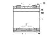
図1は、本発明の太陽電池の一実施例を模式的に示す断面図である。該太陽電池100は、半導体太陽電池基板としての第一導電型のシリコン単結晶基板66(以下、単に基板66と記載する:本実施形態ではp型とする)の第一主表面側に、第二導電型層のエミッタ層65(本実施形態ではn型とする)が形成され、基板面内方向にp−n接合面167が形成されている。エミッタ層65の主表面には、出力取出用の電極63が形成されている。エミッタ層65は太陽電池の受光面を形成するので、p−n接合面167への光の入射効率を高めるために、電極63は、AlあるいはAg等により、例えば内部抵抗低減のため適当な間隔で形成された太いバスバー電極と、そのバスバー電極から所定間隔で櫛型に分岐するフィンガー電極とを有するものとして構成できる。そして、エミッタ層65の電極63の非形成領域が、窒化珪素からなる受光面側絶縁膜61にて覆われている。
【0037】
他方、基板66の第二主表面(裏面)は、窒化珪素からなる裏面側絶縁膜62にて覆われてなり、当該裏面側絶縁膜62の全面がAl等からなる裏面電極64により覆われている。該裏面電極64は、該裏面側絶縁膜62を貫通する導通部(コンタクトホール)を介して基板66の裏面と導通してなる。
【0038】
シリコン単結晶基板66は、FZ(Floating Zone Melting)法及びCZ(Czochralski)法のいずれを用いてもよい。また、シリコン単結晶基板66に代えてGaAs単結晶基板や多結晶シリコン基板を用いることもできる。シリコン単結晶基板66を用いる場合は、結晶製造時にホウ素、ガリウムなどのIII族元素がドープされたp型基板を用いてもよく、又はリン、ヒ素などのV族元素がドープされたn型基板を用いてもよいが、本実施形態では上記のごとくp型基板を用いている。なお、基板抵抗は0.1Ω・cm以上10Ω・cm以下、望ましくは0.5Ω・cm以上2Ω・cm以下とすることが、高性能の太陽電池を実現する上で好適である。また、基板厚さについては、50μm程度であれば、入射した光を太陽電池内にとらえることが可能であり、コスト面でも有利であるが、その後の基板への加工に対して十分な機械的強度を持つためには、150〜300μmであることが望ましい。
【0039】
受光面側絶縁膜61は、水素含有率が1原子%以上10原子%以下、望ましくは1原子%以上5原子%以下の低水素含有無機絶縁膜として構成されている。その屈折率は2以上2.5以下であり、反射防止膜を兼ねている。さらに、Si/N原子比が0.80以上1.80以下である。他方、裏面側絶縁膜62も、Si/N原子比が0.80以上1.80以下の窒化珪素膜とされている(本実施形態においては、屈折率は2以上2.5以下であり、水素含有率は1原子%以上10原子%以下、望ましくは1原子%以上5原子%以下である)。これらはいずれも、反応容器内に半導体太陽電池基板とともに熱触媒体を配置し、珪素源ガスと窒素源ガスとを含有する成膜用ガスを熱触媒体と接触させつつ基板表面に供給し、該成膜用ガスの化学反応に基づき生成する窒化珪素を基板表面に堆積させる触媒CVD法により形成されたものである。
【0040】
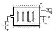
触媒CVD法による薄膜作製の詳細は、例えば特許文献1及び特許文献2により公知であるため、以下簡単に説明する。図2は、本発明に使用できる薄膜作製装置の概略図である。該薄膜作製装置200は、排気装置11により内部が減圧される反応容器1を備え、該反応容器1内に設けられた基板ホルダ21上に基板20が配置される。また、基板ホルダ21上の基板20は、基板ヒーター22(本実施形態では基板ホルダ21内に組み込まれている)により加熱される。さらに、反応容器1には、成膜用ガスを内部に導入するための成膜用ガス導入路31,32と、同じく表面処理用ガスを内部に導入するための表面処理用ガス導入路33と、基板ホルダ21上の基板20に対向する形で容器内に設けられた熱触媒体50と、熱触媒体50を通電加熱する熱触媒体加熱用電源51とが設けられている。
【0041】
排気装置11はターボ分子ポンプやロータリーポンプ等からなる多段の真空ポンプからなり、処理容器内を10−8Torr程度の圧力まで減圧可能とする。成膜用ガス導入路31,32は、成膜用ガスを処理容器内に導入するための円盤状のガス導入ヘッド35に接続されている。ガス導入ヘッド35は、内部が中空であり、前面に多数のガス吹き出し孔を有し、ガス吹き出し孔から成膜用ガスを基板20の主表面(成膜面)に向けて供給するようになっている。
【0042】
熱触媒体50は、ガス導入ヘッド35から基板20に向かう成膜用ガスの流通経路上に配置され、熱触媒体加熱用電源51によって触媒活性化温度、例えば1700℃程度に加熱される。供給された成膜用ガスは、熱触媒体50と接触しつつ基板20の主表面に到達する。成膜用ガスは該接触により分解等の反応が促進されて反応活性種が生じ、基板20上に絶縁材料を堆積させる。本実施形態における熱触媒体50は、直径0.5mm程度のタングステンワイヤーが鋸波状などに加工されたものであり、基板20よりも大きい面積をカバーできるようになっている。なお、基板温度は200℃以上400℃以下の比較的低温でよく、図1において、電極63及び64の形成後であっても、基板66とのコンタクト特性が損なわれる惧れがない。
【0043】
上記のごとく、熱触媒体50を用いた触媒CVD法を採用することにより、従来のようなプラズマを使用することなく成膜が可能となるので、プラズマダメージによる基板表面の損傷や、荷電粒子の混入による絶縁膜の劣化といった問題は原理的になくなる。
なお、該成膜工程は、受光面側絶縁膜61及び裏面側絶縁膜のいずれについても略同様である。なお、成膜用ガス導入路31,32からそれぞれ導入されるシランとアンモニアとの流量を図示しないマスフローコントローラ等でモニタし、バルブ31v,32vにより流量比を制御することで、窒化珪素膜中のSi/N原子比を前記の範囲に調整することができる。なお、シランとアンモニアとは水素ガスによる希釈を行なわない。
【0044】
熱触媒体50は、界面欠陥低減のために成膜前に実施する基板の表面処理にも利用される。シリコン単結晶で構成された基板20の場合、通常、基板表面は自然酸化膜で覆われている。また、基板20の表面の自然酸化膜を予めフッ酸などによって除去した場合においても、通常雰囲気下では酸化が速やかに起こるので、基板表層には酸素原子の結合した珪素原子種が多かれ少なかれ残留する。そこで、絶縁膜を成膜するに先立って、表面処理用ガス導入路33からガス導入ヘッド35を経て、表面処理用ガスとしてのアンモニアガスを反応容器1内に導入する。すると、該アンモニアガスが熱触媒体50との接触分解反応によって活性種に変わり、基板表面を覆っている自然酸化膜の酸素原子(表面再結合のサイトとなりうる)が、窒化珪素からなる絶縁膜の構成原子である窒素原子に置換される。以後、既に説明した触媒CVD法により、絶縁膜の成膜プロセスを連続して行なう。この方法によれば、絶縁膜の組成を均一に保ちながら界面欠陥の少ない絶縁膜を基板上に堆積することができる。
【0045】
なお、上記表面処理を行なうためには表面処理用ガス導入路33が必要であるが、成膜用ガスがシラン(珪素源ガス)とアンモニア(窒素源ガス:アニオン源ガス)の混合ガスであり、表面処理用ガスがアンモニアガスである場合のように、成膜用ガスと同種のガスが表面処理用ガスにも使用される場合、成膜用ガス導入路31を表面処理用ガス導入路に兼用することができる。なお、窒化珪素膜を成膜するための窒素源ガスとしては、上記のアンモニアの他、窒素ガスや他の窒素化合物ガスを用いてもよい。そして、図2の装置構成では、表面処理用ガスもまた、成膜用ガスと同様にガス導入ヘッド35から基板20に供給され、熱触媒体50の表面付近を通過することで、前述したような接触分解反応が生ずることにより、基板20の上記の表面処理反応が促進される。
【0046】
また、熱触媒体50は、成膜後の絶縁膜のパッシベーション特性を向上させるための後処理にも利用される。すなわち、絶縁膜の堆積後に、後処理用ガス導入路34からアンモニアガスや水素ガスなどの後処理用ガスを導入し、表面処理と同様の熱触媒体50によって接触分解反応を引き起こして後処理を行なうことにより、さらに絶縁膜の特性を改善することができる。後処理として周知の水素アニール処理は、水素雰囲気下で、300〜500℃に基板を加熱して行なうが、上記の後処理は、熱触媒体50により分解化学種を積極的に処理容器内に生成させる点が根本的に異なり、分解した化学種が絶縁膜中に拡散してダングリングボンドを封止するためパッシベーション特性が改善されると考えられる。また、該方法によれば、通常の水素アニール処理よりも基板温度を下げられるため(例えば200℃以上400℃以下)、図1において、電極63及び64を形成後に絶縁膜を形成しても、基板66と電極63,64のコンタクト特性を損なう惧れもない。なお、この後処理時に膜中の水素含有量が若干増加する場合があるが、その増加代は1原子%以上3原子%以下の範囲に収まっていることが多く、成膜後の水素含有率が5原子%以下に留まっていれば、最終的な膜中の水素含有率が10原子%を超えることはない。
【0047】
以下、図1の太陽電池100の製造工程の一例について説明する(ここではp型基板を用いた場合について説明するが、n型基板を用いた場合は、「n+」を「p+」と読みかえればよい。ただし、物理的な特性値は異なる)。また、以降の太陽電池作製方法は一例であり、これに限定されるものではない。まず、基板方位が(100)の単結晶シリコン基板(FZ法、Bドープ)66に対し、テクスチャエッチと呼ばれる異方性アルカリエッチングにより、表面に微細なピラミッド状の表面構造を形成する。通常水酸化ナトリウムとアルコールを混合したもの、あるいは炭酸カリウム、炭酸ナトリウムなどを水中に溶解させたものを用い、表面構造の大きさは1〜10μm程度である。この構造により、受光面への入射光が複数回反射しながら基板内部へ効率的に取り込まれる。
【0048】
その後、n+層、すなわちエミッタ層65を形成する。一般的にはリンに代表されるV族元素を、熱拡散、イオン打ち込みなどの公知の方法でドープする。n+層におけるドーパントの表面不純物濃度はシート抵抗が40〜200Ω/□であるように調整することが好ましい。そして、基板裏面の全面に上記の触媒CVD法により窒化珪素からなる裏面側絶縁膜62を形成し、次いでコンタクトホール67の部分をフォトリソグラフィー、機械研削あるいはレーザーアブレーションなどの方法によって開口した後、Al等からなる裏面電極64を真空蒸着法、スパッタ法などによって堆積する。他方、基板66の受光面側は、エミッタ層65を形成する際の拡散時に堆積したリンガラスなどをエッチング除去した後、表面電極63をマスク蒸着などにより堆積し、その後、窒化珪素からなる受光面側絶縁膜61を同様の触媒CVD法により形成する。
【0049】
通常の半導体デバイスのパッシベーション性能の評価は、金属/絶縁体/半導体の積層構造(MIS構造)を形成して、容量−電圧特性(C−V特性)を調べることで見積もることが多い。太陽電池の場合は、拡張Shockley-Read-Hall表面再結合モデルから考察されるように、実効再結合速度は、界面準位密度及び膜中の固定電荷、及び電子とホールとの各捕獲断面積、基板不純物濃度、キャリア注入量などの影響を受ける。また、実験的には、窒化珪素膜中のダングリングボンドによるホールのトラップによりC−V測定においてヒステリシス効果が生じ、またトラップされたホールが紫外線照射など外部要因で解放されることもあるので、基板の履歴も測定結果に影響する。そのため、暗状態でのC−V特性から得られる界面準位密度及び膜中の固定電荷のみで、太陽電池の実際の動作状況を把握することは難しい。そこで裏面のパッシベーション性能の評価においては、バイアス光を測定サンプルに照射することにより、キャリア注入状態を再現しながら太陽電池の動作状況をシミュレーションし、ライフタイムスキャナーを用いて実効ライフタイムを測定することにより、実効表面再結合速度を見積もることが一般に行われている。他方、受光面側、すなわちエミッタ層65側は、高濃度に不純物が注入されているため、C−V測定あるいはDLTS測定の感度が低下し、また深さ方向に拡散の濃度分布があるため実効表面再結合速度の解析が難しい。そのため、受光面側のパッシベーション性能については、実際に太陽電池を作製し、その特性から評価することが多い。
【0050】
従来のプラズマCVD法では、前述のごとくプラズマダメージが大きく、積極的に多量の水素を膜中に導入してダングリングボンドの封止を図る必要があった。本発明においては、受光面側絶縁膜61を触媒CVDにより形成することで、基板66にプラズマダメージが加わらないから非常に良好なパッシベーション特性が得られる。また、プラズマダメージによるダングリングボンドが生じにくいことから、水素を膜中に積極導入する必要がなく、膜組成も窒化珪素の化学量論組成(Si/N原子比=0.75)に近いものを採用すればよいので、プラズマCVD法により大量に水素導入した窒化珪素膜よりも、耐紫外線特性がはるかに良好である。
【0051】
他方、窒化珪素膜の組成を化学量論比から珪素過剰側に大きくシフトさせる必要がないことは、耐紫外線特性が受光面側ほどには問題とならない裏面側絶縁膜64に適用した場合において、別の観点での効果を生ずる。つまり、膜組成が珪素過剰側に過剰にシフトしていないので、その接触界面付近にて基板66側に、図5のような大きな反転層が形成されることが抑制される。その結果、裏面電極64を経由した面内の短絡が効果的に防止され、変換効率の向上がもたらされる。
【0052】
なお、触媒CVD法による成膜処理においては、成膜温度の選定が重要である。例えば、受光面側絶縁層61を反射防止膜として成膜する場合、成膜温度は200℃〜400℃程度が好ましく、なるべく高温に設定することが、堆積される膜中の欠陥もより一層減少するため、パッシベーション特性の点から好ましい。また、基板20の温度は、材料的にも構造的にも熱による変性を受ける温度以下に維持されることが好ましい。なお、図1では電極63をエミッタ層65と接触させているが、これを、Al電極として、受光面側絶縁層61上にMISコンタクト形態で形成する場合は、成膜温度が400℃を超えると、Al電極がエミッタ層を突き抜けるスパイキングを起こし、短絡して性能の低下をもたらす。このため、成膜温度は400℃以下にすることが重要である。
【0053】
また、成膜に先立って前述の表面処理を行なう場合、熱触媒体50の温度は成膜時の触媒温度か、又はそれ以下であることが好ましく、通常1000〜1700℃の範囲で行われる。さらに、成膜後に後処理を行なう場合は、熱触媒体50の温度は表面処理と同様の条件で行われることが好ましく、通常の水素アニール処理を追加、あるいは代用することも基板あるいは電極と基板間のコンタクトの特性を損なわない限り可能である。
【0054】
なお、裏面側絶縁膜62を通常の熱酸化膜として形成することもできる。この場合、周知のドライ酸化、ウェット酸化、パイロジェニック酸化などの手法を採用できる。この際、基板の両面が酸化されるため、裏面にレジストを塗布、乾燥した後、希フッ酸などによって受光面側の酸化膜を除去し、さらにレジストを除去する。この工程により、裏面の絶縁膜62が形成される。
【0055】
【実施例】
以下、本発明の効果を確認するために行なった実験結果について説明する。
(実施例1)
抵抗率1.5Ωcm、3インチ丸形の(100)単結晶シリコン基板(FZ法、Bドープ)を、2%フッ酸で1分洗浄した後、超純水で5分リンスし、乾燥窒素を吹きつけて乾燥した。その後、触媒CVD法により屈折率2.4(Si/N原子比=1.48:水素希釈なし)、膜厚80nmの窒化珪素膜を両面に堆積した。次に、0.5sunの白色バイアス光を照射しながら、実効ライフタイムをライフタイムスキャナーで測定し、同じ基板をケミカルパッシベーション処理(ヨウ素/エタノール処理)したもののライフタイム測定結果を基準として、表面再結合速度を算出した。また、サンプルの片面を400Wのメタルハロゲンランプを光源とし、320nm以下の波長成分をフィルターによってカットした紫外線に32時間及び128時間暴露した後、同様に表面再結合速度を算出した。また、窒化珪素膜中の水素含有率をFT−IR法により分析した。
【0056】
(実施例2)
実施例1と同様の手順でシリコン基板を洗浄、乾燥し、触媒CVD法により、表面処理をアンモニアガスで行い、続いて屈折率2.4の窒化珪素膜を両面に堆積して、同様の測定を行った。
(実施例3)
実施例1と同様の手順でシリコン基板を洗浄、乾燥し、触媒CVD法により、表面処理をアンモニアガスで行い、続いて屈折率2.4の窒化珪素膜を両面に堆積した後、後処理を水素ガスで行い、同様の測定を行った。
【0057】
(比較例1)
実施例1と同様の手順でシリコン基板を洗浄、乾燥し、ダイレクトプラズマCVD法(周波数100kHz:水素希釈なし)により、屈折率2.4の窒化珪素膜を両面に堆積して、同様の測定を行った。
(比較例2)
実施例1と同様の手順でシリコン基板を洗浄、乾燥し、リモートプラズマCVD法(マイクロ波2.5GHz:水素希釈なし)により、屈折率2.4の窒化珪素膜を両面に堆積して、同様の測定を行った。
以上の結果を表1に示す。
【0058】
【表1】
この結果によると、窒化珪素膜を触媒CVDにて形成した実施例1〜実施例3の試験品は、いずれも膜中の水素含有率が5原子%以下と小さく、紫外線照射を継続しても実行表面再結合速度の増加は鈍い。すなわち、耐紫外線特性に優れていることがわかる。しかし、プラズマCVD法を用いた比較例1及び比較例2の試験品は、膜中の水素含有率が非常に高く、紫外線照射継続により実効表面再結合速度は急速に増加しており、実施例1〜実施例3の結果には及ばないことがわかる。
【0060】
(実施例4)
抵抗率0.5Ωcm、厚さ300μm、面寸法100mm×100mmの擬四角形状(100)単結晶シリコン基板(FZ法、Bドープ)を、濃水酸化ナトリウム水溶液中でダメージエッチし、その後水酸化ナトリウム水溶液/イソプロパノール混合溶液中で表面全体にテクスチャを形成した。基板をRCA洗浄した後、高温酸化(1000℃)し、片面をレジストで保護した後、バッファードフッ酸溶液中で酸化膜を片面だけエッチングした。レジストを除去した後、オキシ塩化リンをソースとしたリン拡散を830℃で行い、表面のシート抵抗が100Ω/□となるように拡散した。その後、表面のリンガラスを2%フッ酸で除去し、マスク蒸着によって受光面電極(Ti/Pd/Ag)を蒸着した。裏面は機械加工により溝を形成し、その上から裏面電極(Al)を蒸着した。その後、受光面側に触媒CVD法によって屈折率が2.1(Si/N原子比=1.04:水素希釈なし)、膜厚が80nmの窒化珪素膜を堆積した。完成した太陽電池の特性評価をソーラーシミュレータ(1.5sun)で測定した。
【0061】
(実施例5)
実施例4と同様に裏面電極まで形成し、受光面側に触媒CVD法による表面処理をアンモニアガスで行い、続いて屈折率2.1の窒化珪素膜を堆積して、同様の測定を行った。
(実施例6)
実施例4と同様に裏面電極まで形成し、受光面側に触媒CVD法による表面処理をアンモニアガスで行い、続いて屈折率2.1の窒化珪素膜を堆積した後、後処理を水素ガスで行い、同様の測定を行った。
【0062】
(比較例3)
実施例4と同様に裏面電極まで形成し、受光面側にダイレクトプラズマCVD法(周波数100kHz)により、屈折率2.1の窒化珪素膜を堆積して、同様の測定を行った。
(比較例4)
実施例4と同様に裏面電極まで形成し、受光面側にリモートプラズマCVD法(マイクロ波2.5GHz)により、屈折率2.1の窒化珪素膜を堆積して、同様の測定を行った。
以上の結果を表2に示す。
【0063】
【表2】
この結果によると、窒化珪素膜を触媒CVDにて形成した実施例4〜実施例6の試験品は、いずれも、変換効率を含めた全ての太陽電池特性において、プラズマCVD法を用いた比較例3及び比較例4の試験品の結果を凌駕していることがわかる。また、実施例5及び実施例6のごとく、成膜前の基板表面処理及び後処理を同じ触媒を用いて行なうと、その差は一層顕著となっていることもわかる。
【0065】
(実施例7)
抵抗率0.5Ωcm、厚さ300μm、面寸法100mm×100mmの擬四角形状(100)単結晶シリコン基板(FZ法、Bドープ)を、濃水酸化ナトリウム水溶液中でダメージエッチし、その後水酸化ナトリウム水溶液/イソプロパノール混合溶液中で表面全体にテクスチャを形成した。基板を2枚背中合わせにしてオキシ塩化リンをソースとしたリン拡散を830℃で行い、表面のシート抵抗が100Ω/□となるように拡散した。その後、表面のリンガラスを2%フッ酸で除去し、マスク蒸着によって受光面電極(Ti/Pd/Ag)を蒸着した。裏面は触媒CVD法による表面処理をアンモニアガスで行い、続いて屈折率が2.0(Si/N原子比=0.91:水素希釈なし)、膜厚が80nmの窒化珪素膜を堆積した後、機械加工により溝を形成し、その上から裏面電極(Al)を蒸着した。その後、受光面側に触媒CVD法によって屈折率が2.1(Si/N原子比=1.04:水素希釈なし)、膜厚が80nmの窒化珪素膜を堆積した。完成した太陽電池の特性評価をソーラーシミュレータ(1.5sun)で測定した。
【0066】
(実施例8)
裏面は触媒CVD法による表面処理をアンモニアガスで行い、続いて屈折率が2.0、膜厚が80nmの窒化珪素膜を堆積した後、後処理を水素ガスで行ったこと以外は、実施例7と同様に作製した太陽電池の特性評価をソーラーシミュレータ(1.5sun)で測定した。
(比較例5)
実施例7と同様に表面電極までを形成し、ダイレクトプラズマCVD法(周波数100kHz)により、裏面に屈折率2.0、受光面側に屈折率2.1の窒化珪素膜を堆積したこと以外は同様の工程を経て太陽電池を測定した。
【0067】
(比較例6)
実施例7と同様に表面電極までを形成し、リモートプラズマCVD法(マイクロ波2.5GHz)により、裏面に屈折率2.0、受光面側に屈折率2.1の窒化珪素膜を堆積したこと以外は同様の工程を経て太陽電池を測定した。
以上の結果を表3に示す。
【0068】
【表3】
この結果によると、窒化珪素膜を触媒CVDにて形成した実施例7及び実施例8の試験品は、いずれも、変換効率を含めた全ての太陽電池特性において、プラズマCVD法を用いた比較例5及び比較例6の試験品の結果を凌駕していることがわかる。また、実施例5及び実施例6のごとく、成膜前の基板表面処理及び後処理を同じ触媒を用いて行なうと、その差は一層顕著となっていることもわかる。また、裏面側に窒化珪素膜を形成する場合、触媒CVDを用いた実施例7及び実施例8の結果は表2の結果と同様に良好であるが、プラズマCVD法を用いた比較例5及び比較例6は、裏面側に窒化珪素膜を形成することにより特性が却って悪化していることがわかる。これは、比較例の窒化珪素膜がフィールド効果パッシベーションとなるため、基板側の反転層が大きくなり、図5の短絡が顕著になったためであると考えられる。
【図面の簡単な説明】
【図1】本発明の太陽電池の断面概略図。
【図2】本発明の太陽電池の製造方法に用いる薄膜作製装置の概略図。
【図3】バッチ式平行平板ダイレクトプラズマCVD装置の概略図。
【図4】枚葉式リモートプラズマCVD装置の概略図。
【図5】裏面電極近傍での短絡を説明した概略図。
【符号の説明】
1 反応容器
20 基板
50 熱触媒体
61 受光面側絶縁膜
62 裏面絶縁膜
63 受光面電極
64 裏面電極
65 エミッタ層
66 シリコン単結晶基板(半導体太陽電池基板)
100 太陽電池[0001]
BACKGROUND OF THE INVENTION
The present invention relates to a solar cell that directly converts light energy into electric energy and a method for manufacturing the solar cell.
[0002]
[Prior art]
[Patent Document 1]
Japanese Patent Laid-Open No. 10-83988
[Patent Document 2]
JP-A-8-250438
[0003]
A solar cell is a semiconductor element that converts light energy into electric power, and includes a pn junction type, a pin type, a Schottky type, and the pn junction type is widely used. In addition, when solar cells are classified based on their substrate materials, they can be broadly divided into three types: silicon crystal solar cells, amorphous (amorphous) silicon solar cells, and compound semiconductor solar cells. Silicon crystal solar cells are further classified into single crystal solar cells and polycrystalline solar cells. Since silicon crystal substrates for solar cells can be manufactured relatively easily, silicon crystal solar cells are most popular.
[0004]
The output characteristics of the solar cell as described above are generally evaluated by measuring an output current voltage curve using a solar simulator. On this curve, the point Pm at which the product Ip · Vp of the output current Ip and the output voltage Vp is maximum is called the maximum output Pm, and the total light energy (S × I: S is the element) incident on the solar cell. Area, I is the value divided by the intensity of the irradiated light):
η≡ {Pm / (S × I)} × 100 (%) (1)
Is defined as the conversion efficiency η of the solar cell. In order to increase the conversion efficiency η, the short circuit current Isc (output current value when V = 0 on the current-voltage curve) or the open circuit voltage Voc (also output voltage value when I = 0) is increased, and It is important to make the output current voltage curve as close to square as possible. Note that the degree of squareness of the output current voltage curve is generally
FF≡Ipm × Vpm / (Isc × Voc) (2)
It means that the output current-voltage curve approaches an ideal square shape and the conversion efficiency η increases as the value of the FF is closer to 1.
[0005]
In order to improve the conversion efficiency η, it is important to reduce the surface recombination of carriers (electrons and holes). Specifically, in a solar cell using single crystal silicon or polycrystalline silicon as a substrate, minority carriers photogenerated by incident light such as sunlight reach the pn junction surface mainly by diffusion. After that, it is taken out as majority carriers from the electrodes attached to the light receiving surface and the back surface, and becomes electric energy. At that time, carriers that could be extracted as current through the interface states existing on the substrate surface other than the electrode surface may be recombined and lost, leading to a decrease in conversion efficiency η.
[0006]
Therefore, in the high-efficiency solar cell, the light receiving surface and the back surface of the semiconductor substrate are protected with an insulating film except for the contact portion with the electrode, and carrier recombination at the interface between the semiconductor substrate and each insulating film is suppressed, The conversion efficiency η is improved (so-called surface passivation effect). As such an insulating film, a silicon oxide film has been used for a long time, but its refractive index is as low as about 1.4 and the reflection loss when used on the light-receiving surface side is somewhat large. Since silicon nitride having a refractive index is excellent not only in the passivation effect but also in the antireflection effect, it has been widely used. The silicon nitride film is conventionally formed by a CVD method (Chemical Vapor Deposition) such as thermal CVD, plasma CVD, or photo-CVD. Of these, the most common is plasma CVD.
[0007]
FIG. 3 schematically shows a batch type parallel plate plasma CVD apparatus generally called direct plasma CVD. The apparatus includes a
[0008]
[Problems to be solved by the invention]
Since plasma CVD has a relatively high deposition rate even when the substrate temperature is as low as 400 ° C. or lower, it is frequently used in a manufacturing process for solar cells. However, since the high-energy charged particles generated in the plasma are likely to damage the deposited film and the substrate surface (so-called plasma damage), the resulting silicon nitride film has a high interface state density and a sufficient passivation effect. There is a problem that cannot be obtained. In addition, various characteristics of the solar cell are easily affected.
[0009]
Therefore, a CVD method using ECR (electron cyclotron resonance) plasma has been proposed as a method for suppressing plasma damage. FIG. 4 schematically shows an example of the apparatus. Unlike conventional plasma CVD, this method is characterized in that the substrate surface to be processed is arranged at a position away from the plasma region (plasma zone) in order to separate and use radical species. This is called remote plasma CVD. Specifically, after a predetermined film-forming gas is introduced into the
[0010]
However, in any case, as long as plasma CVD is used, the plasma damage is still large, and the formation of dangling bonds in the film becomes significant, so a large amount of hydrogen is added to the film for improving the passivation effect. It was necessary to contain the dangling bonds by inclusion (in addition, in the known plasma CVD, there is a background in which a large amount of hydrogen derived from the source gas is necessarily taken in). As a result, the silicon nitride film obtained contains as many as 40 atom% hydrogen atoms, and there is a problem that the passivation effect deteriorates with time if irradiation with light containing a large amount of ultraviolet rays such as sunlight is continued.
[0011]
In addition, in a silicon nitride film formed by plasma CVD, the film composition has been considerably shifted from the stoichiometric ratio to the silicon excess side in order to obtain so-called field effect passivation. That is, when the film composition is greatly deviated to the silicon excess side, electrons generated by anion deficiency flow out to the semiconductor substrate side, and the positive charge on the cation side forms a fixed charge, resulting in band bending. Then, since an inversion layer in which electrons are excessive is formed on the semiconductor substrate side in the vicinity of the contact interface, the passivation effect can be enhanced using this.
[0012]
However, this structure has major drawbacks as follows.
(1) When used as a back electrode, as shown in FIG. 5, the
{Circle around (2)} Field effect passivation is noticeable only when applied to the p-type layer side of the substrate due to inversion layer formation by electron outflow. In a solar cell, carriers generated by photoexcitation in the p-type region and n-type region of the substrate are minority carriers, and the main part of the substrate that contributes to light absorption is a p-type substrate in which electrons with a long lifetime become minority carriers. However, in this case, a sufficient passivation effect cannot be exhibited on the light receiving surface side where the n-type emitter layer is formed. Further, since the dopant concentration on the surface of the emitter layer is too high, band bending hardly occurs at a fixed charge level in the silicon nitride film, and the above-mentioned field effect passivation cannot be expected. Therefore, in the emitter layer, suppression of plasma damage, and consequently suppression of interface states, is the key to good passivation characteristics. However, since it is difficult to suppress damage by normal plasma CVD, a good passivation effect cannot be obtained after all.
[0013]
An object of the present invention is to provide a solar cell having an insulating film which is excellent in the passivation effect and hardly causes deterioration of the passivation effect over time, and a method for manufacturing the solar cell.
[0014]
[Means for solving the problems and actions / effects]
In order to solve the above problems, a first solar cell of the present invention is a semiconductor solar in which a light receiving surface is formed on a first main surface and a photovoltaic power is generated based on light irradiated on the light receiving surface. A light-receiving surface side insulating film as an inorganic insulating film made of an inorganic insulating material (hereinafter also referred to as a silicon-based insulating material) whose cation component is mainly silicon. The light-receiving surface side insulating film is formed as a low hydrogen content inorganic insulating film having a hydrogen content of less than 10 atomic%. In this specification, “the main component of the cation component is silicon” means that 50% or more (preferably 80% or more) of the cation component of the inorganic insulating material is silicon. In addition, as long as the effect of this invention demonstrated below is achieved, cations other than silicon may be contained in the range by which the insulation of a material is not impaired too much. For example, an alkali metal ion having a large ion radius such as a cesium cation may be introduced into the nitride film to increase the fixed charge in the film, thereby contributing to field effect passivation.
[0015]
According to the first aspect of the solar cell of the present invention, the light-receiving surface side insulating film is composed of a silicon-based insulating material having a high dielectric constant and a good passivation effect, and the hydrogen content is less than 10 atomic%. Since it is configured as a low hydrogen-containing inorganic insulating film, the durability of the light-receiving surface side insulating film against ultraviolet rays can be greatly improved. Specifically, even when used in an environment where light containing a large amount of ultraviolet rays is irradiated for a long period of time, such as sunlight or fluorescent lamps, the passivation effect of the insulating film is unlikely to deteriorate over time, and thus the conversion efficiency η is prolonged. It can be maintained at a good value over time.
[0016]
The silicon-based insulating film can be formed by a CVD method. And the 1st of the manufacturing method of the solar cell of this invention is a pn junction for generating a photoelectromotive force based on the light irradiated to this light-receiving surface while a light-receiving surface is formed in one main surface. In a method for manufacturing a solar cell, the light-receiving surface of the semiconductor solar cell substrate is covered with a light-receiving surface side insulating film made of an inorganic insulating film whose main cation component is silicon. A light-receiving surface side insulating film, a thermal catalyst body is disposed together with a semiconductor solar cell substrate in a reaction vessel, and contains a silicon source gas and an anion source gas that generates an anion component that binds to silicon in an inorganic material to be obtained. In addition, at least one of the silicon source gas and the anion source gas supplies a film-forming gas having hydrogen atoms in the gas molecules to the surface of the semiconductor solar cell substrate in contact with the thermal catalyst, Gas chemistry The inorganic insulating material produced based on the response catalyst CVD method is deposited on the surface of the semiconductor solar cell substrate, the hydrogen content and forming a low-hydrogen-containing inorganic insulating film 10 atomic% or less.
[0017]
The catalytic CVD method itself is known from
[0018]
As described above, when the catalytic CVD method is used, an insulating film with few interface defects can be deposited on the substrate while keeping the composition of the insulating film uniform, and thus a silicon-based insulating film having a very excellent passivation effect can be obtained. Can do. According to the catalytic CVD method, since the reaction efficiency is enhanced by the catalyst, a high-quality insulating film can be deposited without excessively diluting the film forming gas with a carrier gas such as hydrogen. In addition, the residual amount of hydrogen derived from the film forming gas can be kept small. The effect is that a composition that suppresses the formation of dangling bonds on silicon atoms that easily form bonds with hydrogen (for example, in the case of silicon nitride, the composition is not so far away from the stoichiometric ratio on the silicon-excess side). It becomes particularly large when selected. For these reasons, it is possible to easily realize a silicon-based insulating film having a hydrogen content of 10 atomic% or less while using the CVD method. In order to reduce the hydrogen content in the film, it is more effective to employ a method of supplying the film forming gas to the reaction vessel without diluting with hydrogen.
[0019]
In the present invention, the semiconductor solar cell substrate can be composed of single crystal silicon, polycrystalline silicon, gallium arsenide, germanium, or a composite material thereof, as in the known solar cell. In particular, in consideration of the balance between conversion efficiency and price, it is desirable to use a single crystal silicon substrate as a semiconductor solar cell substrate (the same applies to the second and third solar cells of the present invention below).
[0020]
In the first solar cell of the present invention, the second main surface of the semiconductor solar cell substrate is covered with a back side insulating film as an inorganic insulating film made of an inorganic insulating material whose main cation component is silicon. The back electrode covering the back-side insulating film has a structure in which the back-side electrode is electrically connected to the back surface of the semiconductor solar cell substrate through a conductive portion penetrating the back-side insulating film. Can be configured as a low hydrogen-containing inorganic insulating film with less than 10 atomic%. In a double-sided solar cell in which the back electrode does not cover the entire back side insulating film and incident light from the back side also contributes to power generation, the back side insulating film should also be configured as a low hydrogen-containing inorganic insulating film. Similarly to the light-receiving surface side insulating film, it is possible to improve the anti-ultraviolet characteristics and thus the temporal stability of the passivation effect.
[0021]
If the hydrogen content of the low hydrogen-containing inorganic insulating film exceeds 10 atomic%, the passivation effect tends to deteriorate due to ultraviolet irradiation, and the object of the present invention cannot be achieved. On the other hand, if the hydrogen content of the low-hydrogen-containing inorganic insulating film is less than 1 atomic%, the effect of improving the UV resistance is saturated, and there is a concern that the cost may increase due to complicated processes. Accordingly, the hydrogen content of the low hydrogen content inorganic insulating film is desirably adjusted within a range of 1 atomic% to 10 atomic%, and more desirably 1 atomic% to 5 atomic%.
[0022]
In the present invention, the silicon-based inorganic insulating material constituting the light-receiving surface side insulating film or the back surface side insulating film can be specifically composed of any one of silicon nitride, silicon oxide, and silicon oxynitride. Among these, since silicon nitride is excellent in the passivation effect, it can be used effectively in the present invention. Further, since silicon nitride has a large refractive index, when applied to the light-receiving surface side insulating film, there is an advantage that it can also be used as an antireflection film (the same applies to the second and third solar cells of the present invention below). .
[0023]
In particular, the light-receiving surface side insulating film is desirably configured as a low hydrogen-containing inorganic insulating film made of silicon nitride having a refractive index of 2 to 2.5. When the refractive index is less than 2, the antireflection effect becomes inconspicuous, and when the refractive index exceeds 2.5, optical absorption occurs in the light-receiving surface side insulating film in the wavelength region contributing to current conversion of incident light, On the other hand, conversion efficiency is reduced. The light receiving surface side insulating film preferably has a refractive index of 2 or more and 2.1 or less.
[0024]
The refractive index of the silicon nitride film is closely related to its silicon / nitrogen atomic ratio (Si / N atomic ratio), and the refractive index tends to increase as the atomic ratio of silicon increases. Here, when an attempt is made to adjust the refractive index to 2 or more and 2.5 or less, the Si / N atomic ratio is desirably set in the range of 0.80 or more and 1.80 or less by the study of the present inventors. I understood it. The composition is close to the stoichiometric ratio of silicon nitride (Si / N = 0.75), and unlike the case where the conventional plasma CVD method is employed, there is an advantage that dangling bonds on silicon atoms are less likely to occur. . As a result, combined with the good reaction efficiency of catalytic CVD for producing silicon nitride, the amount of hydrogen remaining in the film derived from the film-forming gas can be greatly reduced (10 atomic% or less; Alternatively, the deterioration with time of the passivation effect when irradiated with ultraviolet rays can be extremely effectively suppressed.
[0025]
When the inorganic insulating film to be obtained is the silicon nitride film, a film forming gas is used in the reaction vessel, and a silicon source gas is used so that silicon nitride having an Si / N atomic ratio of 0.80 to 1.80 is obtained. What is necessary is just to adjust and supply the mixing ratio of nitrogen source gas which makes an anion source gas. For example, if the silicon source gas is silane (referred to generically as silicon hydride: specifically monosilane, disilane, etc.) and the nitrogen source gas is ammonia, the ratio of supply flow rate of silane and ammonia into the reaction vessel Thus, the Si / N atomic ratio of the obtained silicon nitride film can be adjusted. The Si / N atomic ratio of the silicon nitride film can also be adjusted by the pressure of the mixed gas of the silicon source gas and the nitrogen source gas. Specifically, when the mixing ratio of the silicon source gas and the nitrogen source gas is constant, when the gas pressure is high, the gas is rich in nitrogen, and conversely, when the gas pressure is low, the silicon is rich. The Si / N atomic ratio of the silicon nitride film can be adjusted.
[0026]
In the first solar cell of the present invention, the backside insulating film is a film forming gas containing a silicon solar cell substrate and a thermal catalyst body together with a semiconductor solar cell substrate and containing a silicon source gas and a nitrogen source gas. Is supplied to the surface of the semiconductor solar cell substrate in contact with the thermal catalyst, and silicon / nitride generated based on the chemical reaction of the film-forming gas is deposited on the surface of the semiconductor solar cell substrate by catalytic CVD, A silicon nitride film can be formed so that the N atomic ratio is 0.80 or more and 1.80 or less.
[0027]
The second of the solar cells of the present invention is
A light receiving surface is formed on the first main surface, and a semiconductor solar cell substrate that generates photovoltaic power based on light irradiated on the light receiving surface is provided, and the second main surface of the semiconductor solar cell substrate is nitrided The back surface electrode, which is covered with a back side insulating film as an inorganic insulating film made of silicon, and covers the back side insulating film, is connected to the back side of the semiconductor solar cell substrate through a conduction portion that penetrates the back side insulating film. While having a structure formed by conduction,
The silicon nitride film constituting the back-side insulating film is formed by placing a thermal catalyst body together with a semiconductor solar cell substrate in a reaction vessel and bringing a film-forming gas containing a silicon source gas and a nitrogen source gas into contact with the thermal catalyst body. The Si / N atomic ratio is 0.80 by a catalytic CVD method in which silicon nitride produced on the surface of the semiconductor solar cell substrate is deposited on the surface of the semiconductor solar cell substrate. It is formed so that it may become 1.80 or less.
[0028]
Furthermore, the second of the manufacturing methods of the solar cell of this invention is:
A light receiving surface is formed on the first main surface, and a semiconductor solar cell substrate that generates photovoltaic power based on light irradiated on the light receiving surface is provided, and the second main surface of the semiconductor solar cell substrate is nitrided The back surface electrode, which is covered with a back side insulating film as an inorganic insulating film made of silicon, and covers the back side insulating film, is connected to the back side of the semiconductor solar cell substrate through a conduction portion that penetrates the back side insulating film. In a method for manufacturing a solar cell having a conductive structure,
A silicon nitride film constituting the back side insulating film is disposed in a reaction vessel together with a semiconductor solar cell substrate, a thermal catalyst body, and a film forming gas containing a silicon source gas and a nitrogen source gas is brought into contact with the thermal catalyst body. The Si / N atomic ratio is 0.80 by a catalytic CVD method in which silicon nitride produced on the surface of the semiconductor solar cell substrate is deposited on the surface of the semiconductor solar cell substrate. It is formed by adjusting the mixing ratio of the silicon source gas and the nitrogen source gas so as to be 1.80 or less. As described above, silane and ammonia can be used as the silicon source gas and the nitrogen source gas.
[0029]
By forming the back side insulating film as a silicon nitride film having a Si / N atomic ratio of 0.80 or more and 1.80 or less by the catalytic CVD method as described above, the following new peculiar to the back side insulating film as follows: The effect will be produced. That is, by employing the catalytic CVD method, a silicon nitride film having a composition in which the Si / N atomic ratio is close to the stoichiometric ratio as described above can be formed as a low defect film with few dangling bonds. Since such a film has a composition close to the stoichiometric ratio, there is little fixed charge derived from electrons due to silicon excess, and band bending is less likely to occur when bonded to the back surface of the semiconductor solar cell substrate. Therefore, the inversion layer formed on the substrate side is also narrow, and a short circuit within the back electrode surface as shown in FIG. In addition, since a defect such as a dangling bond that becomes a surface recombination site is hardly formed, a good passivation effect can be obtained. In addition, since the hydrogen content can be reduced by setting the Si / N atomic ratio of the silicon nitride film to 0.80 or more and 1.80 or less, the back electrode does not cover the entire back side insulating film and is incident from the back side. In a double-sided light-receiving solar cell in which light also contributes to power generation, as with the light-receiving surface side insulating film, it is possible to improve the anti-ultraviolet characteristics and thus the temporal stability of the passivation effect.
[0030]
As described above, a high-quality silicon nitride film with few defects can be obtained by a catalytic CVD method with a composition close to the stoichiometric ratio of Si / N atomic ratio of 0.80 to 1.80. Thus, a good passivation effect can be obtained without relying on field effect passivation involving the polarity of the inversion layer. As a result, the silicon nitride film differs from a silicon-rich silicon nitride film as an insulating film on the light-receiving surface side. In addition, any of the insulating films on the back side can be used, and each of them can exhibit a unique effect.
[0031]
Next, in the first and second aspects of the solar cell and the method for producing the same of the present invention, the inorganic insulating film introduces a surface treatment gas into the reaction vessel, and brings the surface treatment gas into contact with the thermal catalyst. However, after supplying the surface of the semiconductor solar cell substrate to the surface of the semiconductor solar cell substrate, it can be deposited by catalytic CVD on the surface of the semiconductor solar cell substrate after the surface treatment. In normal plasma CVD, a transition layer containing oxygen atoms, such as a silicon nitride oxide film in the case of a silicon nitride film, is formed in a minute amount at the interface between the substrate and the insulating film, which may cause interface defects. If the surface treatment is performed, the transition layer can be effectively removed, the generation of interface defects can be more effectively suppressed, and the conversion efficiency reduction of the solar cell due to surface recombination can be more effectively prevented. . When the semiconductor solar cell substrate is a silicon substrate and the inorganic insulating film is a silicon nitride film, it is appropriate to use, for example, ammonia gas as the surface treatment gas.
[0032]
In the first and second solar cells of the present invention and the manufacturing method thereof, the inorganic insulating film is deposited on the surface of the semiconductor solar cell substrate by catalytic CVD, and then a post-treatment gas is introduced into the reaction vessel. The post-treatment gas can be post-treated by supplying it to the surface of the inorganic insulating film while being in contact with the thermal catalyst.
[0033]
Furthermore, the third of the solar cells of the present invention is
A light receiving surface is formed on the first main surface, and a semiconductor solar cell substrate that generates a photovoltaic power based on light irradiated on the light receiving surface is provided, and the second main surface of the semiconductor solar cell substrate is a cation It is covered with a back side insulating film as an inorganic insulating film made of an inorganic insulating film whose main component is silicon, and a back electrode that covers the back side insulating film has a conductive portion that penetrates the back side insulating film. And having a structure that is electrically connected to the back surface of the semiconductor solar cell substrate,
The inorganic insulating film is for film formation in which a thermal catalyst is disposed together with a semiconductor solar cell substrate in a reaction vessel, and contains a silicon source gas and an anion source gas that generates an anion component that binds to silicon in the inorganic material to be obtained. Gas is supplied to the surface of the semiconductor solar cell substrate in contact with the thermal catalyst, and an inorganic insulating material generated based on the chemical reaction of the film-forming gas is deposited by catalytic CVD, which is deposited on the surface of the semiconductor solar cell substrate. After the formation, the post-treatment gas is introduced into the reaction vessel, and the post-treatment gas is obtained by supplying the post-treatment gas to the surface of the inorganic insulating film while being in contact with the thermal catalyst. It is characterized by being.
[0034]
Furthermore, the third method for producing the solar cell of the present invention is:
A light receiving surface is formed on the first main surface, and a semiconductor solar cell substrate that generates a photovoltaic power based on light irradiated on the light receiving surface is provided, and the second main surface of the semiconductor solar cell substrate is a cation The semiconductor solar cell is covered with a back-side insulating film made of an inorganic insulating film whose main component is silicon, and the back-side electrode covering the back-side insulating film passes through the conduction portion passing through the back-side insulating film In the manufacturing method of the solar cell having a structure formed by conduction with the back surface of the substrate,
An inorganic insulating film is used for film formation in which a thermal catalyst is disposed in a reaction vessel together with a semiconductor solar cell substrate and contains a silicon source gas and an anion source gas that generates an anion component that binds to silicon in the inorganic material to be obtained. Gas is supplied to the surface of the semiconductor solar cell substrate in contact with the thermal catalyst, and an inorganic insulating material generated based on the chemical reaction of the film-forming gas is deposited by catalytic CVD, which is deposited on the surface of the semiconductor solar cell substrate. After the formation, introducing the post-treatment gas into the reaction vessel, and post-treating the inorganic insulating film by supplying the post-treatment gas to the surface of the inorganic insulating film while being in contact with the thermal catalyst. Features.
[0035]
After depositing the inorganic insulating film, the inventor causes a catalytic decomposition reaction to the post-treatment gas by the thermal catalyst similar to the above-described surface treatment, and supplies this to the surface of the inorganic insulating film for post-processing. As a result, it was found that the passivation characteristics of the insulating film were further improved. In addition, the post-treatment performed by heating in a hydrogen atmosphere without using a catalyst after film formation is called hydrogen annealing treatment, and the method using a catalyst as in the present invention is compared with this. The effect of improving passivation is far superior. The reason for this is presumably because decomposition chemical species are positively generated in the processing vessel by a catalytic reaction, and the decomposed chemical species diffuse into the insulating film to seal dangling bonds. According to this method, since the substrate temperature can be lowered as compared with the normal hydrogen annealing treatment, the post-treatment can be performed stably without impairing the characteristics of the electrode / substrate contact compared to the hydrogen annealing treatment. There are also advantages that can be made.
[0036]
DETAILED DESCRIPTION OF THE INVENTION
FIG. 1 is a cross-sectional view schematically showing one embodiment of the solar cell of the present invention. The
[0037]
On the other hand, the second main surface (back surface) of the
[0038]
The silicon
[0039]
The light-receiving surface
[0040]
Details of thin film production by catalytic CVD are known, for example, from
[0041]
The
[0042]
The
[0043]
As described above, by adopting the catalytic CVD method using the
The film forming process is substantially the same for both the light-receiving surface
[0044]
The
[0045]
In order to perform the above surface treatment, the surface treatment
[0046]
The
[0047]
Hereinafter, an example of a manufacturing process of the
[0048]
Then n+A layer, that is, an emitter layer 65 is formed. Generally, a group V element typified by phosphorus is doped by a known method such as thermal diffusion or ion implantation. n+It is preferable to adjust the surface impurity concentration of the dopant in the layer so that the sheet resistance is 40 to 200Ω / □. Then, a back-
[0049]
The evaluation of the passivation performance of a normal semiconductor device is often estimated by forming a metal / insulator / semiconductor laminated structure (MIS structure) and examining capacitance-voltage characteristics (CV characteristics). In the case of solar cells, the effective recombination rate depends on the interface state density and the fixed charge in the film, as well as the respective capture cross sections of electrons and holes, as considered from the extended Shockley-Read-Hall surface recombination model. Influenced by substrate impurity concentration, carrier injection amount, and the like. Also, experimentally, a hysteresis effect occurs in CV measurement due to trapping of holes due to dangling bonds in the silicon nitride film, and the trapped holes may be released due to external factors such as ultraviolet irradiation. The history of the board also affects the measurement results. Therefore, it is difficult to grasp the actual operation state of the solar cell only with the interface state density obtained from the CV characteristics in the dark state and the fixed charge in the film. Therefore, in the evaluation of the passivation performance on the back side, by irradiating the measurement sample with bias light, the operating state of the solar cell is simulated while reproducing the carrier injection state, and the effective lifetime is measured using a lifetime scanner. Thus, the effective surface recombination rate is generally estimated by On the other hand, since the impurity is implanted at a high concentration on the light receiving surface side, that is, the emitter layer 65 side, the sensitivity of CV measurement or DLTS measurement is reduced, and the diffusion concentration distribution in the depth direction is effective. Analysis of surface recombination velocity is difficult. For this reason, the passivation performance on the light receiving surface side is often evaluated by actually producing a solar cell and its characteristics.
[0050]
In the conventional plasma CVD method, plasma damage is large as described above, and it has been necessary to actively introduce a large amount of hydrogen into the film to seal dangling bonds. In the present invention, since the light-receiving surface
[0051]
On the other hand, the fact that the composition of the silicon nitride film does not need to be greatly shifted from the stoichiometric ratio to the silicon-excess side is applied to the back-
[0052]
In the film formation process by the catalytic CVD method, the selection of the film formation temperature is important. For example, when the light-receiving surface
[0053]
Moreover, when performing the above-mentioned surface treatment prior to film formation, the temperature of the
[0054]
The back
[0055]
【Example】
Hereinafter, experimental results performed to confirm the effects of the present invention will be described.
Example 1
Resistivity 1.5Ωcm, 3-inch round (100) single crystal silicon substrate (FZ method, B-doped) washed with 2% hydrofluoric acid for 1 minute, rinsed with ultrapure water for 5 minutes, and dried nitrogen Sprayed dry. Thereafter, a silicon nitride film having a refractive index of 2.4 (Si / N atomic ratio = 1.48: no hydrogen dilution) and a film thickness of 80 nm was deposited on both surfaces by catalytic CVD. Next, the effective lifetime was measured with a lifetime scanner while irradiating 0.5 sun white bias light, and the surface was re-measured based on the lifetime measurement results of the same substrate subjected to chemical passivation treatment (iodine / ethanol treatment). The binding rate was calculated. In addition, the surface recombination rate was calculated in the same manner after exposing one side of the sample to ultraviolet light obtained by using a 400 W metal halogen lamp as a light source and cutting a wavelength component of 320 nm or less by a filter for 32 hours and 128 hours. Further, the hydrogen content in the silicon nitride film was analyzed by the FT-IR method.
[0056]
(Example 2)
The silicon substrate was cleaned and dried in the same procedure as in Example 1, and surface treatment was performed with ammonia gas by catalytic CVD, followed by deposition of a silicon nitride film having a refractive index of 2.4 on both surfaces, and the same measurement. Went.
(Example 3)
The silicon substrate is cleaned and dried in the same procedure as in Example 1, and the surface treatment is performed with ammonia gas by catalytic CVD. Subsequently, a silicon nitride film having a refractive index of 2.4 is deposited on both surfaces, and then post-treatment is performed. The same measurement was performed using hydrogen gas.
[0057]
(Comparative Example 1)
The silicon substrate was cleaned and dried in the same procedure as in Example 1, and a silicon nitride film having a refractive index of 2.4 was deposited on both sides by the direct plasma CVD method (
(Comparative Example 2)
The silicon substrate was cleaned and dried in the same procedure as in Example 1, and a silicon nitride film having a refractive index of 2.4 was deposited on both sides by remote plasma CVD (microwave 2.5 GHz: no hydrogen dilution). Was measured.
The results are shown in Table 1.
[0058]
[Table 1]
According to this result, all of the test products of Examples 1 to 3 in which the silicon nitride film was formed by catalytic CVD had a small hydrogen content in the film of 5 atomic% or less, and the ultraviolet irradiation was continued. The increase in effective surface recombination rate is slow. That is, it can be seen that the ultraviolet resistance is excellent. However, the test products of Comparative Example 1 and Comparative Example 2 using the plasma CVD method have a very high hydrogen content in the film, and the effective surface recombination rate is rapidly increased by continuing the ultraviolet irradiation. It turns out that it does not reach the result of 1-Example 3.
[0060]
Example 4
A pseudo-square (100) single crystal silicon substrate (FZ method, B-doped) having a resistivity of 0.5 Ωcm, a thickness of 300 μm, and a surface dimension of 100 mm × 100 mm is damaged and etched in a concentrated sodium hydroxide aqueous solution, and then sodium hydroxide The entire surface was textured in an aqueous solution / isopropanol mixed solution. After the substrate was washed with RCA, it was oxidized at a high temperature (1000 ° C.), one side was protected with a resist, and then the oxide film was etched only on one side in a buffered hydrofluoric acid solution. After removing the resist, phosphorus diffusion using phosphorus oxychloride as a source was performed at 830 ° C., and diffusion was performed so that the sheet resistance of the surface was 100Ω / □. Thereafter, the phosphorous glass on the surface was removed with 2% hydrofluoric acid, and a light-receiving surface electrode (Ti / Pd / Ag) was deposited by mask deposition. A groove was formed on the back surface by machining, and a back electrode (Al) was deposited thereon. Thereafter, a silicon nitride film having a refractive index of 2.1 (Si / N atomic ratio = 1.04: no hydrogen dilution) and a film thickness of 80 nm was deposited on the light receiving surface side by catalytic CVD. Characteristic evaluation of the completed solar cell was measured with a solar simulator (1.5 sun).
[0061]
(Example 5)
The back electrode was formed in the same manner as in Example 4, surface treatment by catalytic CVD was performed on the light receiving surface side with ammonia gas, and a silicon nitride film having a refractive index of 2.1 was subsequently deposited, and the same measurement was performed. .
(Example 6)
The back electrode is formed in the same manner as in Example 4, and surface treatment by catalytic CVD is performed on the light receiving surface side with ammonia gas. Subsequently, a silicon nitride film having a refractive index of 2.1 is deposited, and then post treatment is performed with hydrogen gas. The same measurement was performed.
[0062]
(Comparative Example 3)
A back electrode was formed in the same manner as in Example 4, and a silicon nitride film having a refractive index of 2.1 was deposited on the light receiving surface side by a direct plasma CVD method (frequency: 100 kHz), and the same measurement was performed.
(Comparative Example 4)
Similar to Example 4, a back electrode was formed, and a silicon nitride film having a refractive index of 2.1 was deposited on the light receiving surface side by a remote plasma CVD method (microwave 2.5 GHz), and the same measurement was performed.
The results are shown in Table 2.
[0063]
[Table 2]
According to this result, the test products of Examples 4 to 6 in which the silicon nitride film was formed by catalytic CVD were all comparative examples using the plasma CVD method in all solar cell characteristics including conversion efficiency. It can be seen that the results of the test products of No. 3 and Comparative Example 4 were exceeded. In addition, as in Example 5 and Example 6, when the substrate surface treatment before film formation and the post-treatment are performed using the same catalyst, the difference is further noticeable.
[0065]
(Example 7)
A pseudo-square (100) single crystal silicon substrate (FZ method, B-doped) having a resistivity of 0.5 Ωcm, a thickness of 300 μm, and a surface dimension of 100 mm × 100 mm is damaged and etched in a concentrated sodium hydroxide aqueous solution, and then sodium hydroxide The entire surface was textured in an aqueous solution / isopropanol mixed solution. Two substrates were back-to-back, and phosphorus diffusion using phosphorus oxychloride as a source was performed at 830 ° C. so that the sheet resistance of the surface was 100Ω / □. Thereafter, the phosphorous glass on the surface was removed with 2% hydrofluoric acid, and a light-receiving surface electrode (Ti / Pd / Ag) was deposited by mask deposition. After the back surface is subjected to surface treatment by catalytic CVD method with ammonia gas, and subsequently a silicon nitride film having a refractive index of 2.0 (Si / N atomic ratio = 0.91: no hydrogen dilution) and a film thickness of 80 nm is deposited. Then, a groove was formed by machining, and a back electrode (Al) was deposited from above. Thereafter, a silicon nitride film having a refractive index of 2.1 (Si / N atomic ratio = 1.04: no hydrogen dilution) and a film thickness of 80 nm was deposited on the light receiving surface side by catalytic CVD. Characteristic evaluation of the completed solar cell was measured with a solar simulator (1.5 sun).
[0066]
(Example 8)
Except that the back surface was subjected to surface treatment by catalytic CVD method with ammonia gas, and subsequently a silicon nitride film having a refractive index of 2.0 and a film thickness of 80 nm was deposited, followed by post-treatment with hydrogen gas. The characteristic evaluation of the solar cell produced similarly to 7 was measured with a solar simulator (1.5 sun).
(Comparative Example 5)
Except for forming up to the surface electrode as in Example 7 and depositing a silicon nitride film having a refractive index of 2.0 on the back surface and a refractive index of 2.1 on the light receiving surface side by direct plasma CVD (
[0067]
(Comparative Example 6)
A surface electrode was formed in the same manner as in Example 7, and a silicon nitride film having a refractive index of 2.0 on the back surface and a refractive index of 2.1 on the light-receiving surface side was deposited by remote plasma CVD (microwave 2.5 GHz). The solar cell was measured through the same process except that.
The above results are shown in Table 3.
[0068]
[Table 3]
According to this result, the test products of Example 7 and Example 8 in which the silicon nitride film was formed by catalytic CVD were all comparative examples using the plasma CVD method in all solar cell characteristics including conversion efficiency. It can be seen that the results of the test products of No. 5 and Comparative Example 6 are surpassed. In addition, as in Example 5 and Example 6, when the substrate surface treatment before film formation and the post-treatment are performed using the same catalyst, the difference is further noticeable. Further, when the silicon nitride film is formed on the back side, the results of Example 7 and Example 8 using catalytic CVD are as good as the results of Table 2, but Comparative Example 5 using plasma CVD and It can be seen that the characteristics of Comparative Example 6 are worsened by forming a silicon nitride film on the back side. This is probably because the silicon nitride film of the comparative example is field effect passivation, the inversion layer on the substrate side becomes large, and the short circuit in FIG. 5 becomes prominent.
[Brief description of the drawings]
FIG. 1 is a schematic cross-sectional view of a solar cell of the present invention.
FIG. 2 is a schematic view of a thin film production apparatus used in the method for producing a solar cell of the present invention.
FIG. 3 is a schematic view of a batch-type parallel plate direct plasma CVD apparatus.
FIG. 4 is a schematic view of a single wafer type remote plasma CVD apparatus.
FIG. 5 is a schematic diagram illustrating a short circuit near the back electrode.
[Explanation of symbols]
1 reaction vessel
20 substrates
50 Thermal catalyst
61 Insulating film on light-receiving surface side
62 Back surface insulation film
63 Light-receiving surface electrode
64 Back electrode
65 Emitter layer
66 Silicon single crystal substrate (semiconductor solar cell substrate)
100 solar cells
Claims (10)
Translated fromJapanese前記裏面側絶縁膜を構成する窒化珪素膜を、反応容器内に前記半導体太陽電池基板とともに熱触媒体を配置し、珪素源ガスと窒素源ガスとを含有する成膜用ガスを前記熱触媒体と接触させつつ前記半導体太陽電池基板の表面に供給し、該成膜用ガスの化学反応に基づき生成する窒化珪素を該半導体太陽電池基板の表面に堆積させる触媒CVD法により、Si/N原子比が0.80以上1.80以下となるように、前記珪素源ガスと前記窒素源ガスとの混合比を調整して形成することを特徴とする太陽電池の製造方法。 A thermal catalyst is disposed in a reaction vessel together with the semiconductor solar cell substrate, and a film forming gas containing a silicon source gas and a nitrogen source gas is used as the thermal catalyst. Si / N atomic ratio by catalytic CVD method in which silicon nitride generated based on the chemical reaction of the film-forming gas is deposited on the surface of the semiconductor solar cell substrate while being brought into contact with the surface of the semiconductor solar cell substrate Is formed by adjusting the mixing ratio of the silicon source gas and the nitrogen source gas so as to be 0.80 or more and 1.80 or less.
前記裏面側絶縁膜を、反応容器内に前記半導体太陽電池基板とともに熱触媒体を配置し、珪素源ガスと、得るべき無機材料において珪素と結合するアニオン成分を生成するアニオン源ガスとを含有する成膜用ガスを前記熱触媒体と接触させつつ前記半導体太陽電池基板の表面に供給し、該成膜用ガスの化学反応に基づき生成する無機絶縁材料を該半導体太 The back side insulating film includes a thermal catalyst body together with the semiconductor solar cell substrate in a reaction vessel, and contains a silicon source gas and an anion source gas that generates an anion component that binds to silicon in the inorganic material to be obtained. A film-forming gas is supplied to the surface of the semiconductor solar cell substrate in contact with the thermal catalyst, and an inorganic insulating material generated based on a chemical reaction of the film-forming gas is formed on the semiconductor thick film.陽電池基板の表面に堆積させる触媒CVD法により堆積・形成した後、前記反応容器内に後処理用ガスを導入し、該後処理用ガスを前記熱触媒体と接触させつつ当該裏面側絶縁膜の表面に供給することにより前記無機絶縁膜を後処理することを特徴とする請求項1記載の太陽電池の製造方法。After being deposited and formed by the catalytic CVD method to be deposited on the surface of the positive cell substrate, a post-treatment gas is introduced into the reaction vessel, and the back-side insulating film is brought into contact with the thermal catalyst body The method for manufacturing a solar cell according to claim 1, wherein the inorganic insulating film is post-processed by being supplied to a surface of the solar cell.
Priority Applications (8)
| Application Number | Priority Date | Filing Date | Title |
|---|---|---|---|
| JP2003131797AJP4118187B2 (en) | 2003-05-09 | 2003-05-09 | Manufacturing method of solar cell |
| CNB2004800125302ACN100530700C (en) | 2003-05-09 | 2004-03-29 | Solar cell and process for producing same |
| AU2004237524AAU2004237524B2 (en) | 2003-05-09 | 2004-03-29 | Solar cell and process for producing the same |
| US10/556,063US20070186970A1 (en) | 2003-05-09 | 2004-03-29 | Solar cell and method of fabricating the same |
| EP04724198AEP1630873A4 (en) | 2003-05-09 | 2004-03-29 | SOLAR CELL AND METHOD OF MANUFACTURING THE SAME |
| KR1020057021348AKR101058735B1 (en) | 2003-05-09 | 2004-03-29 | Solar cell and manufacturing method |
| PCT/JP2004/004405WO2004100273A1 (en) | 2003-05-09 | 2004-03-29 | Solar cell and process for producing the same |
| US12/656,360US8030223B2 (en) | 2003-05-09 | 2010-01-27 | Solar cell and method of fabricating the same |
Applications Claiming Priority (1)
| Application Number | Priority Date | Filing Date | Title |
|---|---|---|---|
| JP2003131797AJP4118187B2 (en) | 2003-05-09 | 2003-05-09 | Manufacturing method of solar cell |
Publications (2)
| Publication Number | Publication Date |
|---|---|
| JP2004335867A JP2004335867A (en) | 2004-11-25 |
| JP4118187B2true JP4118187B2 (en) | 2008-07-16 |
Family
ID=33432145
Family Applications (1)
| Application Number | Title | Priority Date | Filing Date |
|---|---|---|---|
| JP2003131797AExpired - Fee RelatedJP4118187B2 (en) | 2003-05-09 | 2003-05-09 | Manufacturing method of solar cell |
Country Status (7)
| Country | Link |
|---|---|
| US (2) | US20070186970A1 (en) |
| EP (1) | EP1630873A4 (en) |
| JP (1) | JP4118187B2 (en) |
| KR (1) | KR101058735B1 (en) |
| CN (1) | CN100530700C (en) |
| AU (1) | AU2004237524B2 (en) |
| WO (1) | WO2004100273A1 (en) |
Cited By (1)
| Publication number | Priority date | Publication date | Assignee | Title |
|---|---|---|---|---|
| JPH06320145A (en)* | 1993-05-11 | 1994-11-22 | Nippon Kiyuushiyoku Setsubi Kk | Purifier automatically discharging stagnated water |
Families Citing this family (81)
| Publication number | Priority date | Publication date | Assignee | Title |
|---|---|---|---|---|
| US20060130891A1 (en)* | 2004-10-29 | 2006-06-22 | Carlson David E | Back-contact photovoltaic cells |
| US7765949B2 (en)* | 2005-11-17 | 2010-08-03 | Palo Alto Research Center Incorporated | Extrusion/dispensing systems and methods |
| US20070107773A1 (en)* | 2005-11-17 | 2007-05-17 | Palo Alto Research Center Incorporated | Bifacial cell with extruded gridline metallization |
| JP4489035B2 (en)* | 2006-02-27 | 2010-06-23 | シャープ株式会社 | Photoelectric conversion element |
| US20080314429A1 (en)* | 2007-02-09 | 2008-12-25 | Stichting Imec Nederland | Method for Thermal Matching of a Thermoelectric Generator with a Heat Source Having High Thermal Resistance and Thermoelectric Generator thus Obtained |
| US7993700B2 (en)* | 2007-03-01 | 2011-08-09 | Applied Materials, Inc. | Silicon nitride passivation for a solar cell |
| JP5022743B2 (en)* | 2007-03-13 | 2012-09-12 | シャープ株式会社 | Photoelectric conversion element |
| EP1976034A3 (en)* | 2007-03-29 | 2011-11-09 | Stichting IMEC Nederland | Method for manufacturing a thermopile, the thermopile thus obtrained and a thermoelectric generator comprising such thermopiles |
| JP5117770B2 (en)* | 2007-06-12 | 2013-01-16 | シャープ株式会社 | Manufacturing method of solar cell |
| AT505168B1 (en)* | 2007-06-29 | 2008-11-15 | Span Gerhard Dipl Ing Dr | THERMOELECTRIC ELEMENT |
| JP5124189B2 (en)* | 2007-07-11 | 2013-01-23 | シャープ株式会社 | Method for manufacturing photoelectric conversion element |
| JP5173370B2 (en)* | 2007-11-21 | 2013-04-03 | シャープ株式会社 | Method for manufacturing photoelectric conversion element |
| KR101474008B1 (en) | 2007-12-12 | 2014-12-18 | 엘지전자 주식회사 | Method for preparing of solar cell using plasma-surface-treatment |
| KR101437162B1 (en)* | 2007-12-12 | 2014-09-03 | 엘지전자 주식회사 | Method for manufacturing solar cell using plasma surface treatment |
| US8198528B2 (en)* | 2007-12-14 | 2012-06-12 | Sunpower Corporation | Anti-reflective coating with high optical absorption layer for backside contact solar cells |
| KR101000064B1 (en) | 2007-12-18 | 2010-12-10 | 엘지전자 주식회사 | Heterojunction solar cell and its manufacturing method |
| EP2088630A1 (en)* | 2008-02-08 | 2009-08-12 | Applied Materials, Inc. | Photovoltaic device comprising a sputter deposited passivation layer as well as method and apparatus for producing such a device |
| US8481357B2 (en) | 2008-03-08 | 2013-07-09 | Crystal Solar Incorporated | Thin film solar cell with ceramic handling layer |
| EP2195853B1 (en)* | 2008-04-17 | 2015-12-16 | LG Electronics Inc. | Solar cell and method of manufacturing the same |
| KR100984701B1 (en)* | 2008-08-01 | 2010-10-01 | 엘지전자 주식회사 | Manufacturing method of solar cell |
| US20110168263A1 (en)* | 2008-09-18 | 2011-07-14 | The Regents Of The University Of California | Design of higher efficiency silicon solar cells |
| TWI366919B (en)* | 2008-09-19 | 2012-06-21 | Gintech Energy Corp | Structure of solar cell and its production method |
| US8916769B2 (en) | 2008-10-01 | 2014-12-23 | International Business Machines Corporation | Tandem nanofilm interconnected semiconductor wafer solar cells |
| US8101856B2 (en)* | 2008-10-02 | 2012-01-24 | International Business Machines Corporation | Quantum well GaP/Si tandem photovoltaic cells |
| TWI382554B (en) | 2008-10-30 | 2013-01-11 | Au Optronics Corp | Light sensing element and manufacturing method thereof |
| US20100108134A1 (en)* | 2008-10-31 | 2010-05-06 | Crystal Solar, Inc. | Thin two sided single crystal solar cell and manufacturing process thereof |
| US20100108130A1 (en)* | 2008-10-31 | 2010-05-06 | Crystal Solar, Inc. | Thin Interdigitated backside contact solar cell and manufacturing process thereof |
| CN103904168B (en)* | 2008-12-02 | 2016-06-08 | 三菱电机株式会社 | The manufacture method of solar battery cell |
| US20110284054A1 (en)* | 2009-01-28 | 2011-11-24 | Alliance For Sustainable Energy, Llc | Spectral splitting for multi-bandgap photovoltaic energy conversion |
| TWI390755B (en)* | 2009-03-19 | 2013-03-21 | Ind Tech Res Inst | Solar cell manufacturing method |
| TWI381534B (en)* | 2009-03-24 | 2013-01-01 | Au Optronics Corp | Optical sensor and manufacturing method thereof, and display panel with optical sensor |
| US20100258174A1 (en)* | 2009-04-14 | 2010-10-14 | Michael Ghebrebrhan | Global optimization of thin film photovoltaic cell front coatings |
| WO2010147260A1 (en)* | 2009-06-18 | 2010-12-23 | Lg Electronics Inc. | Solar cell and method of manufacturing the same |
| KR101144810B1 (en) | 2009-07-06 | 2012-05-11 | 엘지전자 주식회사 | Electrode paste for solar cell, solar cell using the paste, and manufacturing method of the solar cell |
| US20110012229A1 (en)* | 2009-07-14 | 2011-01-20 | United Microelectronics Corp. | Semiconductor device with capacitor and method of fabricating the same |
| KR101139459B1 (en) | 2009-08-27 | 2012-04-30 | 엘지전자 주식회사 | Sollar Cell And Fabrication Method Thereof |
| AU2010296714B9 (en) | 2009-09-18 | 2014-12-04 | Shin-Etsu Chemical Co., Ltd. | Solar cell, method for manufacturing solar cell, and solar cell module |
| US9012766B2 (en) | 2009-11-12 | 2015-04-21 | Silevo, Inc. | Aluminum grid as backside conductor on epitaxial silicon thin film solar cells |
| US20110132444A1 (en)* | 2010-01-08 | 2011-06-09 | Meier Daniel L | Solar cell including sputtered reflective layer and method of manufacture thereof |
| JP5397693B2 (en)* | 2010-02-25 | 2014-01-22 | 大日本スクリーン製造株式会社 | Hydrogen content acquisition apparatus and hydrogen content acquisition method |
| JP5535709B2 (en)* | 2010-03-19 | 2014-07-02 | 三洋電機株式会社 | SOLAR CELL, SOLAR CELL MODULE USING THE SOLAR CELL, AND SOLAR CELL MANUFACTURING METHOD |
| JP5623131B2 (en)* | 2010-05-20 | 2014-11-12 | 京セラ株式会社 | SOLAR CELL DEVICE, ITS MANUFACTURING METHOD, AND SOLAR CELL MODULE |
| US9214576B2 (en)* | 2010-06-09 | 2015-12-15 | Solarcity Corporation | Transparent conducting oxide for photovoltaic devices |
| KR101048165B1 (en)* | 2010-08-20 | 2011-07-08 | 현대중공업 주식회사 | Solar cell manufacturing method |
| US9773928B2 (en) | 2010-09-10 | 2017-09-26 | Tesla, Inc. | Solar cell with electroplated metal grid |
| US9800053B2 (en) | 2010-10-08 | 2017-10-24 | Tesla, Inc. | Solar panels with integrated cell-level MPPT devices |
| KR101729744B1 (en)* | 2010-10-19 | 2017-04-24 | 엘지전자 주식회사 | Method for manufacturing solar cell |
| JP5477303B2 (en)* | 2011-01-12 | 2014-04-23 | 信越化学工業株式会社 | Manufacturing method of solar cell |
| US9054256B2 (en) | 2011-06-02 | 2015-06-09 | Solarcity Corporation | Tunneling-junction solar cell with copper grid for concentrated photovoltaic application |
| US10043934B2 (en) | 2011-06-08 | 2018-08-07 | International Business Machines Corporation | Silicon-containing heterojunction photovoltaic element and device |
| DE102011081863A1 (en)* | 2011-08-31 | 2013-02-28 | Robert Bosch Gmbh | Solar cell and process for its production |
| JP6082521B2 (en)* | 2012-01-18 | 2017-02-15 | 旭化成エレクトロニクス株式会社 | Semiconductor element |
| JP2013165160A (en)* | 2012-02-10 | 2013-08-22 | Shin Etsu Chem Co Ltd | Method for manufacturing solar cell, and solar cell |
| TWI457858B (en)* | 2012-02-22 | 2014-10-21 | Chroma Ate Inc | Method for classifying color of a solar cell |
| JP6351601B2 (en) | 2012-10-04 | 2018-07-04 | ソーラーシティ コーポレーション | Photovoltaic device using electroplated metal grid |
| US9865754B2 (en) | 2012-10-10 | 2018-01-09 | Tesla, Inc. | Hole collectors for silicon photovoltaic cells |
| US9281436B2 (en) | 2012-12-28 | 2016-03-08 | Solarcity Corporation | Radio-frequency sputtering system with rotary target for fabricating solar cells |
| US10074755B2 (en) | 2013-01-11 | 2018-09-11 | Tesla, Inc. | High efficiency solar panel |
| US9412884B2 (en) | 2013-01-11 | 2016-08-09 | Solarcity Corporation | Module fabrication of solar cells with low resistivity electrodes |
| US9219174B2 (en) | 2013-01-11 | 2015-12-22 | Solarcity Corporation | Module fabrication of solar cells with low resistivity electrodes |
| US9624595B2 (en) | 2013-05-24 | 2017-04-18 | Solarcity Corporation | Electroplating apparatus with improved throughput |
| JP2015179700A (en)* | 2014-03-18 | 2015-10-08 | キヤノン株式会社 | Manufacturing method of solid-state imaging device |
| KR20150143336A (en)* | 2014-06-12 | 2015-12-23 | 주식회사 케이씨씨 | Multilayer coated substrate for rear surface reflection of photovoltaic module and method for manufacturing the same |
| US10309012B2 (en) | 2014-07-03 | 2019-06-04 | Tesla, Inc. | Wafer carrier for reducing contamination from carbon particles and outgassing |
| JP5830147B1 (en)* | 2014-09-04 | 2015-12-09 | 信越化学工業株式会社 | Solar cell and method for manufacturing solar cell |
| JP2016092238A (en) | 2014-11-05 | 2016-05-23 | 信越化学工業株式会社 | Solar battery and method for manufacturing the same |
| US9899546B2 (en) | 2014-12-05 | 2018-02-20 | Tesla, Inc. | Photovoltaic cells with electrodes adapted to house conductive paste |
| US9947822B2 (en) | 2015-02-02 | 2018-04-17 | Tesla, Inc. | Bifacial photovoltaic module using heterojunction solar cells |
| JP2016197651A (en)* | 2015-04-03 | 2016-11-24 | 株式会社島津製作所 | Thin film and forming method of the same |
| US10035139B2 (en) | 2015-06-29 | 2018-07-31 | Korea Advanced Institute Of Science And Technology | Method for improving solar energy conversion efficiency using metal oxide photocatalysts having energy band of core-shell for ultraviolet ray and visible light absorption and photocatalysts thereof |
| US9761744B2 (en) | 2015-10-22 | 2017-09-12 | Tesla, Inc. | System and method for manufacturing photovoltaic structures with a metal seed layer |
| EP3163632A1 (en) | 2015-11-02 | 2017-05-03 | CSEM Centre Suisse d'Electronique et de Microtechnique SA - Recherche et Développement | Photovoltaic device and method for manufacturing the same |
| US9842956B2 (en) | 2015-12-21 | 2017-12-12 | Tesla, Inc. | System and method for mass-production of high-efficiency photovoltaic structures |
| US9496429B1 (en) | 2015-12-30 | 2016-11-15 | Solarcity Corporation | System and method for tin plating metal electrodes |
| US10115838B2 (en) | 2016-04-19 | 2018-10-30 | Tesla, Inc. | Photovoltaic structures with interlocking busbars |
| CN106298593B (en)* | 2016-08-18 | 2019-12-27 | 四川洪芯微科技有限公司 | High-reliability glass-passivated semiconductor device |
| US10672919B2 (en) | 2017-09-19 | 2020-06-02 | Tesla, Inc. | Moisture-resistant solar cells for solar roof tiles |
| US11190128B2 (en) | 2018-02-27 | 2021-11-30 | Tesla, Inc. | Parallel-connected solar roof tile modules |
| US12132129B2 (en)* | 2020-02-14 | 2024-10-29 | Alliance For Sustainable Energy, Llc | High-performance metal grids for solar cells formed by cracked film lithography |
| CN115036375B (en) | 2021-02-23 | 2023-03-24 | 浙江晶科能源有限公司 | Solar cell, manufacturing method thereof and solar module |
| CN117766595A (en)* | 2021-08-20 | 2024-03-26 | 上海晶科绿能企业管理有限公司 | Solar cells and photovoltaic modules |
Family Cites Families (16)
| Publication number | Priority date | Publication date | Assignee | Title |
|---|---|---|---|---|
| WO1989000341A1 (en)* | 1987-07-07 | 1989-01-12 | Mobil Solar Energy Corporation | Method of fabricating solar cells with anti-reflection coating |
| JP2639616B2 (en) | 1993-03-12 | 1997-08-13 | 株式会社半導体エネルギー研究所 | Semiconductor film formation method |
| JP3231470B2 (en)* | 1993-03-31 | 2001-11-19 | 株式会社リコー | Semiconductor device |
| JP3417072B2 (en) | 1994-08-15 | 2003-06-16 | ソニー株式会社 | Semiconductor device manufacturing method |
| JP3453214B2 (en) | 1995-03-15 | 2003-10-06 | 科学技術振興事業団 | Method of manufacturing thin film transistor by catalytic CVD method and thin film transistor |
| JP3158028B2 (en)* | 1995-07-25 | 2001-04-23 | シャープ株式会社 | Solar cell and method of manufacturing the same |
| JPH09205209A (en)* | 1996-01-26 | 1997-08-05 | Toshiba Electron Eng Corp | Thin film transistor and method of manufacturing the same |
| JPH09244284A (en) | 1996-03-06 | 1997-09-19 | Canon Inc | Method for manufacturing light receiving member |
| JP3737221B2 (en)* | 1996-09-06 | 2006-01-18 | 英樹 松村 | Thin film forming method and thin film forming apparatus |
| JP3141805B2 (en)* | 1997-01-20 | 2001-03-07 | 日本電気株式会社 | Method for manufacturing semiconductor device |
| JP4299393B2 (en)* | 1999-01-20 | 2009-07-22 | 富士通マイクロエレクトロニクス株式会社 | Manufacturing method of semiconductor device |
| JP2002075877A (en) | 2000-08-30 | 2002-03-15 | Kyocera Corp | Method and apparatus for forming polycrystalline semiconductor thin film and solar cell using polycrystalline semiconductor thin film |
| JP2002329876A (en) | 2001-04-26 | 2002-11-15 | Kyocera Corp | Method for manufacturing photoelectric conversion device |
| JP3904883B2 (en) | 2001-10-19 | 2007-04-11 | 京セラ株式会社 | Gas separation type catalytic CVD equipment |
| DE60221426T2 (en)* | 2001-11-26 | 2007-11-29 | Shell Solar Gmbh | SOLAR CELL WITH BACK CONTACT and METHOD OF MANUFACTURE |
| JP3868324B2 (en)* | 2002-04-15 | 2007-01-17 | 三菱電機株式会社 | Silicon nitride film forming method, film forming apparatus, and semiconductor device manufacturing method |
- 2003
- 2003-05-09JPJP2003131797Apatent/JP4118187B2/ennot_activeExpired - Fee Related
- 2004
- 2004-03-29CNCNB2004800125302Apatent/CN100530700C/ennot_activeExpired - Lifetime
- 2004-03-29AUAU2004237524Apatent/AU2004237524B2/ennot_activeExpired
- 2004-03-29USUS10/556,063patent/US20070186970A1/ennot_activeAbandoned
- 2004-03-29KRKR1020057021348Apatent/KR101058735B1/ennot_activeExpired - Fee Related
- 2004-03-29WOPCT/JP2004/004405patent/WO2004100273A1/enactiveApplication Filing
- 2004-03-29EPEP04724198Apatent/EP1630873A4/ennot_activeWithdrawn
- 2010
- 2010-01-27USUS12/656,360patent/US8030223B2/ennot_activeExpired - Fee Related
Cited By (1)
| Publication number | Priority date | Publication date | Assignee | Title |
|---|---|---|---|---|
| JPH06320145A (en)* | 1993-05-11 | 1994-11-22 | Nippon Kiyuushiyoku Setsubi Kk | Purifier automatically discharging stagnated water |
Also Published As
| Publication number | Publication date |
|---|---|
| US8030223B2 (en) | 2011-10-04 |
| AU2004237524B2 (en) | 2009-09-17 |
| EP1630873A4 (en) | 2007-03-14 |
| US20100173447A1 (en) | 2010-07-08 |
| KR101058735B1 (en) | 2011-08-22 |
| CN100530700C (en) | 2009-08-19 |
| US20070186970A1 (en) | 2007-08-16 |
| CN1784789A (en) | 2006-06-07 |
| EP1630873A1 (en) | 2006-03-01 |
| JP2004335867A (en) | 2004-11-25 |
| WO2004100273A1 (en) | 2004-11-18 |
| AU2004237524A1 (en) | 2004-11-18 |
| KR20060064561A (en) | 2006-06-13 |
Similar Documents
| Publication | Publication Date | Title |
|---|---|---|
| JP4118187B2 (en) | Manufacturing method of solar cell | |
| CN108110065B (en) | Back contact solar cell and preparation method thereof | |
| JP3722326B2 (en) | Manufacturing method of solar cell | |
| CN103456804B (en) | Form the method for inverted pyramid type porous surface nanometer texture on the polysilicon and prepare the method for shortwave enhancement mode solar cell | |
| JP5456168B2 (en) | Method for manufacturing photoelectric conversion device | |
| RU2532137C2 (en) | Solar cell, solar cell fabrication method and solar cell module | |
| JP5490231B2 (en) | SOLAR CELL DEVICE, ITS MANUFACTURING METHOD, AND SOLAR CELL MODULE | |
| KR101654691B1 (en) | A method for cleaning the surface of a silicon substrate | |
| JP5058184B2 (en) | Method for manufacturing photovoltaic device | |
| CN102986042A (en) | Method for producing a photovoltaic solar cell | |
| RU2456709C2 (en) | Solar cell and method and apparatus for making said solar cell | |
| CN110943143A (en) | Method for manufacturing a photovoltaic solar cell with heterojunction and emitter diffusion regions | |
| CN117766623B (en) | A method for preparing a solar cell, a solar cell and a photovoltaic module | |
| TW201515244A (en) | Solar battery and solar battery module | |
| CN116936675A (en) | Passivation contact structure, solar cell manufacturing method and solar cell | |
| JP4486622B2 (en) | Manufacturing method of solar cell | |
| KR102674774B1 (en) | High photoelectric conversion efficiency solar cell and manufacturing method of high photoelectric conversion efficiency solar cell | |
| JP5623131B2 (en) | SOLAR CELL DEVICE, ITS MANUFACTURING METHOD, AND SOLAR CELL MODULE | |
| CN103746006A (en) | Passivating layer of crystalline silicon solar cell and passivating process thereof | |
| CN108074990A (en) | UV curing of light-receiving surfaces of solar cells | |
| Morisset | Integration of poly-Si/SiOx contacts in silicon solar cells: Optimization and understanding of conduction and passivation properties | |
| JP2005167291A (en) | Method for manufacturing solar cell and method for manufacturing semiconductor device | |
| JP2011199276A (en) | Surface treatment method and method for manufacturing solar cell | |
| JP5516611B2 (en) | Solar cell manufacturing method and solar cell | |
| KR102118905B1 (en) | Solar cell including a tunnel oxide layer and method of manufacturing the same |
Legal Events
| Date | Code | Title | Description |
|---|---|---|---|
| A711 | Notification of change in applicant | Free format text:JAPANESE INTERMEDIATE CODE: A711 Effective date:20031027 | |
| A521 | Request for written amendment filed | Free format text:JAPANESE INTERMEDIATE CODE: A821 Effective date:20031028 | |
| A711 | Notification of change in applicant | Free format text:JAPANESE INTERMEDIATE CODE: A712 Effective date:20040818 | |
| A621 | Written request for application examination | Free format text:JAPANESE INTERMEDIATE CODE: A621 Effective date:20050222 | |
| A871 | Explanation of circumstances concerning accelerated examination | Free format text:JAPANESE INTERMEDIATE CODE: A871 Effective date:20050913 | |
| A131 | Notification of reasons for refusal | Free format text:JAPANESE INTERMEDIATE CODE: A131 Effective date:20051212 | |
| A521 | Request for written amendment filed | Free format text:JAPANESE INTERMEDIATE CODE: A523 Effective date:20060209 | |
| A521 | Request for written amendment filed | Free format text:JAPANESE INTERMEDIATE CODE: A523 Effective date:20060210 | |
| A975 | Report on accelerated examination | Free format text:JAPANESE INTERMEDIATE CODE: A971005 Effective date:20051205 | |
| A521 | Request for written amendment filed | Free format text:JAPANESE INTERMEDIATE CODE: A523 Effective date:20060224 | |
| RD02 | Notification of acceptance of power of attorney | Free format text:JAPANESE INTERMEDIATE CODE: A7422 Effective date:20060224 | |
| A521 | Request for written amendment filed | Free format text:JAPANESE INTERMEDIATE CODE: A821 Effective date:20060224 | |
| A02 | Decision of refusal | Free format text:JAPANESE INTERMEDIATE CODE: A02 Effective date:20060531 | |
| A711 | Notification of change in applicant | Free format text:JAPANESE INTERMEDIATE CODE: A711 Effective date:20060628 | |
| A521 | Request for written amendment filed | Free format text:JAPANESE INTERMEDIATE CODE: A821 Effective date:20060628 | |
| A521 | Request for written amendment filed | Free format text:JAPANESE INTERMEDIATE CODE: A523 Effective date:20060731 | |
| A621 | Written request for application examination | Free format text:JAPANESE INTERMEDIATE CODE: A621 Effective date:20050222 | |
| A911 | Transfer to examiner for re-examination before appeal (zenchi) | Free format text:JAPANESE INTERMEDIATE CODE: A911 Effective date:20060925 | |
| A912 | Re-examination (zenchi) completed and case transferred to appeal board | Free format text:JAPANESE INTERMEDIATE CODE: A912 Effective date:20061013 | |
| A61 | First payment of annual fees (during grant procedure) | Free format text:JAPANESE INTERMEDIATE CODE: A61 Effective date:20080422 | |
| R150 | Certificate of patent or registration of utility model | Ref document number:4118187 Country of ref document:JP Free format text:JAPANESE INTERMEDIATE CODE: R150 Free format text:JAPANESE INTERMEDIATE CODE: R150 | |
| FPAY | Renewal fee payment (event date is renewal date of database) | Free format text:PAYMENT UNTIL: 20110502 Year of fee payment:3 | |
| FPAY | Renewal fee payment (event date is renewal date of database) | Free format text:PAYMENT UNTIL: 20140502 Year of fee payment:6 | |
| R250 | Receipt of annual fees | Free format text:JAPANESE INTERMEDIATE CODE: R250 | |
| R250 | Receipt of annual fees | Free format text:JAPANESE INTERMEDIATE CODE: R250 | |
| R250 | Receipt of annual fees | Free format text:JAPANESE INTERMEDIATE CODE: R250 | |
| R250 | Receipt of annual fees | Free format text:JAPANESE INTERMEDIATE CODE: R250 | |
| R250 | Receipt of annual fees | Free format text:JAPANESE INTERMEDIATE CODE: R250 | |
| LAPS | Cancellation because of no payment of annual fees |