JP4107269B2 - Solid-state imaging device - Google Patents
Solid-state imaging deviceDownload PDFInfo
- Publication number
- JP4107269B2 JP4107269B2JP2004208038AJP2004208038AJP4107269B2JP 4107269 B2JP4107269 B2JP 4107269B2JP 2004208038 AJP2004208038 AJP 2004208038AJP 2004208038 AJP2004208038 AJP 2004208038AJP 4107269 B2JP4107269 B2JP 4107269B2
- Authority
- JP
- Japan
- Prior art keywords
- column
- unit
- analog
- digital
- row
- Prior art date
- Legal status (The legal status is an assumption and is not a legal conclusion. Google has not performed a legal analysis and makes no representation as to the accuracy of the status listed.)
- Expired - Lifetime
Links
Images


Classifications
- H—ELECTRICITY
- H04—ELECTRIC COMMUNICATION TECHNIQUE
- H04N—PICTORIAL COMMUNICATION, e.g. TELEVISION
- H04N25/00—Circuitry of solid-state image sensors [SSIS]; Control thereof
- H04N25/70—SSIS architectures; Circuits associated therewith
- H04N25/76—Addressed sensors, e.g. MOS or CMOS sensors
- H04N25/77—Pixel circuitry, e.g. memories, A/D converters, pixel amplifiers, shared circuits or shared components
- H04N25/772—Pixel circuitry, e.g. memories, A/D converters, pixel amplifiers, shared circuits or shared components comprising A/D, V/T, V/F, I/T or I/F converters
- H—ELECTRICITY
- H03—ELECTRONIC CIRCUITRY
- H03M—CODING; DECODING; CODE CONVERSION IN GENERAL
- H03M1/00—Analogue/digital conversion; Digital/analogue conversion
- H03M1/10—Calibration or testing
- H03M1/1009—Calibration
- H03M1/1014—Calibration at one point of the transfer characteristic, i.e. by adjusting a single reference value, e.g. bias or gain error
- H03M1/1023—Offset correction
- H—ELECTRICITY
- H04—ELECTRIC COMMUNICATION TECHNIQUE
- H04N—PICTORIAL COMMUNICATION, e.g. TELEVISION
- H04N23/00—Cameras or camera modules comprising electronic image sensors; Control thereof
- H04N23/50—Constructional details
- H04N23/54—Mounting of pick-up tubes, electronic image sensors, deviation or focusing coils
- H—ELECTRICITY
- H04—ELECTRIC COMMUNICATION TECHNIQUE
- H04N—PICTORIAL COMMUNICATION, e.g. TELEVISION
- H04N25/00—Circuitry of solid-state image sensors [SSIS]; Control thereof
- H04N25/40—Extracting pixel data from image sensors by controlling scanning circuits, e.g. by modifying the number of pixels sampled or to be sampled
- H04N25/46—Extracting pixel data from image sensors by controlling scanning circuits, e.g. by modifying the number of pixels sampled or to be sampled by combining or binning pixels
- H—ELECTRICITY
- H04—ELECTRIC COMMUNICATION TECHNIQUE
- H04N—PICTORIAL COMMUNICATION, e.g. TELEVISION
- H04N25/00—Circuitry of solid-state image sensors [SSIS]; Control thereof
- H04N25/60—Noise processing, e.g. detecting, correcting, reducing or removing noise
- H04N25/616—Noise processing, e.g. detecting, correcting, reducing or removing noise involving a correlated sampling function, e.g. correlated double sampling [CDS] or triple sampling
- H—ELECTRICITY
- H04—ELECTRIC COMMUNICATION TECHNIQUE
- H04N—PICTORIAL COMMUNICATION, e.g. TELEVISION
- H04N25/00—Circuitry of solid-state image sensors [SSIS]; Control thereof
- H04N25/70—SSIS architectures; Circuits associated therewith
- H04N25/76—Addressed sensors, e.g. MOS or CMOS sensors
- H04N25/767—Horizontal readout lines, multiplexers or registers
- H—ELECTRICITY
- H04—ELECTRIC COMMUNICATION TECHNIQUE
- H04N—PICTORIAL COMMUNICATION, e.g. TELEVISION
- H04N25/00—Circuitry of solid-state image sensors [SSIS]; Control thereof
- H04N25/70—SSIS architectures; Circuits associated therewith
- H04N25/76—Addressed sensors, e.g. MOS or CMOS sensors
- H04N25/78—Readout circuits for addressed sensors, e.g. output amplifiers or A/D converters
- H—ELECTRICITY
- H03—ELECTRONIC CIRCUITRY
- H03M—CODING; DECODING; CODE CONVERSION IN GENERAL
- H03M1/00—Analogue/digital conversion; Digital/analogue conversion
- H03M1/12—Analogue/digital converters
- H03M1/50—Analogue/digital converters with intermediate conversion to time interval
- H03M1/56—Input signal compared with linear ramp
Landscapes
- Engineering & Computer Science (AREA)
- Multimedia (AREA)
- Signal Processing (AREA)
- Theoretical Computer Science (AREA)
- Transforming Light Signals Into Electric Signals (AREA)
- Computer Vision & Pattern Recognition (AREA)
- Solid State Image Pick-Up Elements (AREA)
Abstract
Description
Translated fromJapanese本発明は、固体撮像装置に関し、特に単位画素から列信号線を介して出力されるアナログ信号をデジタル信号に変換して読み出す構成の固体撮像装置に関する。The present invention relatesto a solid-state imagingequipment, relates the analog signal output via the column signal linein the solid-state imagingequipment configuration to be read into a digital signal from the particular unit pixel.
固体撮像装置として、近年、単位画素の行列状(マトリックス状)の配列に対して列毎にアナログ−デジタル変換装置(以下、ADC(Analog-Digital Converter)と略す)を配置してなる列並列ADC搭載のCMOSイメージセンサが報告されている(例えば、非特許文献1参照)。 In recent years, as a solid-state imaging device, an analog-digital conversion device (hereinafter abbreviated as an ADC (Analog-Digital Converter)) is arranged for each column with respect to a matrix-like arrangement of unit pixels. An on-board CMOS image sensor has been reported (for example, see Non-Patent Document 1).
図15は、従来例に係る列並列ADC搭載のCMOSイメージセンサ100の構成を示すブロック図である。 FIG. 15 is a block diagram showing a configuration of a CMOS image sensor 100 equipped with a column parallel ADC according to a conventional example.
図15において、単位画素101は、フォトダイオードおよび画素内アンプを有し、行列状に2次元配置されることによって画素アレイ部102を構成している。この画素アレイ部102の行列状の画素配置に対して、行毎に行制御線103(103−1,103−2,…)が配線され、列毎に列信号線104(104−1,104−2,…)が配線されている。画素アレイ部102の行アドレスや行走査の制御は、行走査回路105により行制御線103−1,103−2,…を介して行われる。 In FIG. 15, a unit pixel 101 has a photodiode and an in-pixel amplifier, and constitutes a pixel array unit 102 by being two-dimensionally arranged in a matrix. For the matrix pixel arrangement of the pixel array unit 102, row control lines 103 (103-1, 103-2,...) Are wired for each row, and column signal lines 104 (104-1, 104) for each column. -2, ...) are wired. Control of the row address and row scanning of the pixel array unit 102 is performed by the
列信号線104−1,104−2,…の一端側には、これら列信号線104−1,104−2,…毎にADC106が配置されてカラム処理部(列並列ADCブロック)107を構成している。また、ADC106の各々に対して、ランプ(RAMP)波形の参照電圧Vrefを生成するデジタル−アナログ変換装置(以下、DAC(Digital-Analog Converter)と略す)108と、所定周期のクロックCKに同期してカウント動作を行うことにより、後述する比較器110で比較動作が行われる時間を計測するカウンタ109とが設けられている。 On one end side of the column signal lines 104-1, 104-2,..., An
ADC106は、行制御線103−1,103−2,…毎に、選択行の単位画素101から列信号線104−1,104−2,…を経由して得られるアナログ信号を、DAC108で生成される参照電圧Vrefと比較する比較器110と、この比較器110の比較出力に応答してカウンタ109のカウント値を保持するメモリ装置111とからなり、単位画素101から与えられるアナログ信号をNビットのデジタル信号に変換する機能を有している。 The ADC 106 generates, for each row control line 103-1, 103-2,..., An analog signal obtained from the unit pixel 101 in the selected row via the column signal lines 104-1, 104-2,. Comparator 110 for comparing with the reference voltage Vref, and a
カラム処理部107のADC106の各々に対する列アドレスや列走査の制御は、列走査回路112によって行われる。すなわち、ADC106の各々でAD変換されたNビットのデジタル信号は、列走査回路112による列走査によって順に2Nビット幅の水平出力線113に読み出され、当該水平出力線113によって信号処理回路114まで伝送される。信号処理回路114は、2Nビット幅の水平出力線113に対応した2N個のセンス回路、減算回路および出力回路などによって構成されている。 The
タイミング制御回路115は、マスタークロックMCKに基づいて行走査回路105、ADC106、DAC108、カウンタ109および列走査回路112などの各動作に必要なクロック信号やタイミング信号を生成し、これらクロック信号やタイミング信号を該当する回路部分に供給する。 The
次に、上記構成の従来例例に係るCMOSイメージセンサ100の動作を、図16のタイミングチャートを用いて説明する。 Next, the operation of the CMOS image sensor 100 according to the conventional example having the above configuration will be described with reference to the timing chart of FIG.
ある選択行の単位画素101からの列信号線104−1,104−2,…への1回目の読み出し動作が安定した後、DAC108からランプ波形の参照電圧Vrefを比較器110に与えることで、当該比較器110において列信号線104−1,104−2,…の信号電圧Vxと参照電圧Vrefとの比較動作が行われる。この比較動作において、参照電圧Vrefと信号電圧Vxとが等しくなったときに、比較器110の出力Vcoの極性が反転する。この比較器110の反転出力を受けて、メモリ装置111には比較器110での比較時間に応じたカウンタ109のカウント値N1が保持される。 After the first reading operation from the unit pixel 101 of a selected row to the column signal lines 104-1, 104-2,... Is stabilized, the
この1回目の読み出し動作では、単位画素101のリセット成分ΔVの読み出しが行われる。このリセット成分ΔV内には、単位画素101毎にばらつく固定パターンノイズがオフセットとして含まれている。しかし、このリセット成分ΔVのばらつきは一般に小さく、またリセットレベルは全画素共通であるため、1回目の読み出し時の列信号線14の信号電圧Vxはおおよそ既知である。したがって、1回目のリセット成分ΔVの読み出し時には、ランプ波形の参照電圧Vrefを調整することにより、比較器110での比較期間を短くすることが可能である。本従来例では、7ビット分のカウント期間(128クロック)でリセット成分ΔVの比較を行っている。 In the first read operation, the reset component ΔV of the unit pixel 101 is read. The reset component ΔV includes fixed pattern noise that varies for each unit pixel 101 as an offset. However, since the variation of the reset component ΔV is generally small and the reset level is common to all the pixels, the signal voltage Vx of the column signal line 14 at the first reading is approximately known. Therefore, at the time of reading the reset component ΔV for the first time, the comparison period in the comparator 110 can be shortened by adjusting the reference voltage Vref of the ramp waveform. In this conventional example, the reset component ΔV is compared in a 7-bit count period (128 clocks).
2回目の読み出しでは、リセット成分ΔVに加え単位画素101毎の入射光量に応じた信号成分の読み出しが、1回目の読み出しと同様の動作によって行われる。すなわち、ある選択行の単位画素101から列信号線104−1,104−2,…への2回目の読み出し動作が安定した後、DAC108からランプ波形の参照電圧Vrefを比較器110に与えることで、当該比較器110において列信号線104−1,104−2,…の信号電圧Vxと参照電圧Vrefとの比較動作が行われる。 In the second reading, in addition to the reset component ΔV, a signal component corresponding to the amount of incident light for each unit pixel 101 is read by the same operation as the first reading. That is, after the second read operation from the unit pixel 101 of a selected row to the column signal lines 104-1, 104-2,... Is stabilized, the ramp waveform reference voltage Vref is supplied from the
参照電圧Vrefが比較器110に与えられると同時に、カウンタ109で2回目のカウントがなされる。そして、2回目の比較動作において、参照電圧Vrefと信号電圧Vxとが等しくなったときに、比較器110の出力Vcoの極性が反転する。この比較器110の反転出力を受けて、メモリ装置111には比較器110での比較時間に応じたカウンタ109のカウント値N2が保持される。このとき、1回目のカウント値N1と2回目のカウント値N2とは、メモリ装置111内の異なった場所に保持される。 At the same time as the reference voltage Vref is supplied to the comparator 110, the
上述した一連のAD変換動作の終了後、列走査回路112による列走査により、メモリ装置111に保持された1回目と2回目のそれぞれNビットのデジタル信号が2N本の水平出力線113を経て信号処理回路114に供給され、当該信号処理回路114内の減算回路(図示せず)において(2回目の信号)−(1回目の信号)の減算処理がなされた後に外部へ出力される。その後、順次行毎に同様の動作が繰り返されることによって2次元画像が生成される。 After completion of the series of AD conversion operations described above, the first and second N-bit digital signals held in the
上記従来例に係る列並列ADC搭載のCMOSイメージセンサでは、メモリ装置111内に1回目と2回目のカウント値N1,N2を保持する必要があり、Nビットの信号に対してメモリ装置111が2N個必要となるため回路規模、回路面積が増大する。また、カウンタ109からN系統のクロックCK1〜CKNをメモリ装置111に入力する必要があるため、クロック雑音の増加や消費電力の増大も懸念される。更に、水平出力線113も1回目と2回目のカウント値N1,N2を出力するために2N本必要となり、またそれに伴う電流増加も生ずる。加えて、外部出力前には、1回目と2回目のカウント値N1,N2を減算するためにN個の減算回路が必要になり、回路規模、回路面積が増大する。 In the CMOS image sensor equipped with the column parallel ADC according to the conventional example, it is necessary to hold the first and second count values N1 and N2 in the
ところで、高速撮像のために、画素情報を間引き読み出し(飛ばし読み出し)することによってフレームレートを向上させる手法が採られる場合がある(例えば、非特許文献2参照)。この手法を採ることにより、図17に示すプログレッシブ走査方式では30フレーム/秒のフレームレートのところを、図18に示すインターレース走査方式(一行間引き)では60フレーム/秒のフレームレートを実現できる。すなわち、出力する画素情報を行単位で間引いて読み出し、読み出し行数を例えば1/2にすればフレームレートを2倍にすることができる。 By the way, for high-speed imaging, there is a case in which a method for improving the frame rate by thinning out pixel information (skipping readout) is employed (for example, see Non-Patent Document 2). By adopting this method, it is possible to realize a frame rate of 30 frames / second in the progressive scanning method shown in FIG. 17, and a frame rate of 60 frames / second in the interlace scanning method (single line thinning) shown in FIG. In other words, if the pixel information to be output is read out by thinning out in units of rows and the number of readout rows is halved, for example, the frame rate can be doubled.
しかしながら、非特許文献2記載の従来技術、即ち画素情報の間引き読み出しによってフレームレートの向上を図る技術では、フレームレートが高くなるにつれて各単位画素における露光時間が短縮され、例えばフレームレートが2倍になれば、露光時間は半分になる。その結果、単位画素の実効的な感度も半分になる。したがって、列並列ADC搭載のCMOSイメージセンサ100において、画素情報の間引き読み出しの技術を適用してフレームレートの向上を図った場合、高フレームレート化によって単位画素の感度が低下するため、撮像結果に感度低下が起こるという課題がある。 However, in the conventional technique described in Non-Patent
本発明は、上記課題に鑑みてなされたものであって、その目的とするところは、感度低下を招くことなく、高フレームレート化を実現可能な固体撮像装置を提供することにある。The present invention was made in view of the above problems, it is an object without causing a reduction in sensitivity is to providea solid-state imagingequipment capable of realizing a high frame rate.
本発明による固体撮像装置は、
光電変換素子を含む単位画素が行列状に2次元配置されるとともに、当該単位画素の行列状配置に対して列毎に列信号線が配線されてなる画素アレイ部と、
前記画素アレイ部の各単位画素を行毎に選択制御する行走査手段と、
前記行走査手段によって選択制御された行の単位画素から前記列信号線を介して出力されるアナログ信号をデジタル信号に変換し、かつ得られたデジタル信号を複数の単位画素間で加算して出力するアナログ−デジタル変換手段と、
前記アナログ−デジタル変換手段で加算されたデジタル信号の出力制御を行う列走査手段と、
前記列走査手段の制御によって前記アナログ−デジタル変換手段から出力されるデジタル信号を伝送する出力線とを備え、
前記アナログ−デジタル変換手段は、
前記単位画素から出力されるアナログ信号を参照電圧と比較する比較手段と、
前記比較手段での比較動作の開始から比較動作の終了までをカウントするカウント手段とを有し、
前記カウント手段にて前記デジタル信号の加算処理を行う
ことを特徴としている。The solid-state imaging device according to the present invention is
With unit pixels including photoelectric conversion elements are two-dimensionally arranged in a matrix,and a pixel array section column signal lineis wired for each column with respect to a matrix arrangement of the unit pixel,
Row scanning means for selectively controllingeach unit pixel of thepixel array section for eachrow;
An analog signal output via the column signal line from the unit pixel in the row controlled and controlled by the row scanning unit is converted into a digital signal, and the obtained digital signal is added between a plurality of unit pixels and output. Analog-to-digital conversion means
Column scanning means for controlling the output of the digital signal added by the analog-digital conversion means;
An output line for transmitting a digital signal output from the analog-to-digital conversion means under the control of the column scanning means,
The analog-digital conversion means includes
Comparison means for comparing an analog signal output from the unit pixel with a reference voltage;
Counting means for counting from the start of the comparison operation in the comparison means until the end of the comparison operation,
The digital signal is added by the counting means.
It is characterized by that.
上記構成の固体撮像装置において、単位画素から出力されるアナログ信号をデジタル値に変換するとともに、当該デジタル値を複数の単位画素間で加算して読み出すことで、読み出した画素情報数の観点からすれば、画素情報の間引き読み出し(飛ばし読み出し)を行ったのと同じことになるが、1つの画素情報についての情報量の観点からすれば、加算する画素の画素数倍となる。したがって、フレームレートを例えば2倍に向上すべく、単位画素の露光時間を1/2にしたとしても、アナログ−デジタル変換の際にデジタル値を2行分の単位画素間で加算することで、1つの画素情報についての情報量が2倍になるため感度低下が起きない。 In the solid-state imaging device having the above-described configuration, the analog signal output from the unit pixel is converted into a digital value, and the digital value is added and read between a plurality of unit pixels, so that the number of read pixel information is reduced. For example, this is the same as performing thinning-out reading (skipping reading) of pixel information, but from the viewpoint of the amount of information for one piece of pixel information, the number of pixels to be added is doubled. Therefore, even if the exposure time of the unit pixel is halved in order to improve the frame rate, for example, by doubling the digital value between the unit pixels for two rows at the time of analog-digital conversion, Since the amount of information for one piece of pixel information is doubled, the sensitivity does not decrease.
本発明によれば、単位画素から列信号線を介して出力されるアナログ信号をデジタル値に変換して読み出す構成の固体撮像装置において、デジタル値を複数の単位画素間で加算して読み出すことにより、単位画素の露光時間を短縮したとしても、結果として1つの画素情報の情報量が減ることはないため、感度低下を招くことなく、高フレームレート化を図ることができる。 According to the present invention, in a solid-state imaging device having a configuration in which an analog signal output from a unit pixel via a column signal line is converted into a digital value and read out, the digital value is added and read among a plurality of unit pixels. Even if the exposure time of the unit pixel is shortened, the information amount of one piece of pixel information does not decrease as a result, so that a high frame rate can be achieved without causing a decrease in sensitivity.
以下、本発明の実施の形態について図面を参照して詳細に説明する。 Hereinafter, embodiments of the present invention will be described in detail with reference to the drawings.
[第1実施形態]
図1は、本発明の第1実施形態に係る固体撮像装置、例えば列並列ADC搭載のCMOSイメージセンサの構成を示すブロック図である。図1に示すように、本実施形態に係るCMOSイメージセンサ10は、光電変換素子を含む単位画素11が行列状(マトリックス状)に多数2次元配置されてなる画素アレイ部12に加えて、行走査回路13、カラム処理部14、参照電圧供給部15、列走査回路16、水平出力線17およびタイミング制御回路18を有する構成となっている。[First Embodiment]
FIG. 1 is a block diagram showing a configuration of a solid-state imaging device according to the first embodiment of the present invention, for example, a CMOS image sensor equipped with a column parallel ADC. As shown in FIG. 1, the CMOS image sensor 10 according to this embodiment includes a row in addition to a pixel array unit 12 in which a large number of
このシステム構成において、タイミング制御回路18は、マスタークロックMCKに基づいて、行走査回路13、カラム処理部14、参照電圧供給部15および列走査回路16などの動作の基準となるクロック信号や制御信号などを生成し、行走査回路13、カラム処理部14、参照電圧供給部15および列走査回路16などに対して与える。 In this system configuration, the
また、画素アレイ部12の各単位画素11を駆動制御する周辺の駆動系や信号処理系、即ち行走査回路13、カラム処理部14、参照電圧供給部15、列走査回路16、水平出力線17およびタイミング制御回路18などは、画素アレイ部12と同一のチップ(半導体基板)19上に集積される。 In addition, peripheral driving systems and signal processing systems that drive and control each
単位画素11としては、ここでは図示を省略するが、光電変換素子(例えば、フォトダイオード)に加えて、例えば、当該光電変換素子で光電変換して得られる電荷をFD(フローティングディフュージョン)部に転送する転送トランジスタと、当該FD部の電位を制御するリセットトランジスタと、FD部の電位に応じた信号を出力する増幅トランジスタとを有する3トランジスタ構成のものや、さらに画素選択を行うための選択トランジスタを別に有する4トランジスタ構成のものなどを用いることができる。 Although not shown here as the
画素アレイ部12には、単位画素11がm列n行分だけ2次元配置されるとともに、このm行n列の画素配置に対して行毎に行制御線21(21−1〜21−n)が配線され、列毎に列信号線22(22−1〜22−m)が配線されている。行制御線21−1〜21−nの各一端は、行走査回路13の各行に対応した各出力端に接続されている。行走査回路13は、シフトレジスタなどによって構成され、行制御線21−1〜21−nを介して画素アレイ部12の行アドレスや行走査の制御を行う。 In the pixel array unit 12,
カラム処理部14は、例えば、画素アレイ部12の画素列毎、即ち列信号線22−1〜22−m毎に設けられたADC(アナログ−デジタル変換回路)23−1〜23−mを有し、画素アレイ部12の各単位画素11から列毎に出力されるアナログ信号をデジタル信号に変換して出力する。本発明ではこれらADC23−1〜23−mの構成を特徴としており、その詳細については後述する。 The column processing unit 14 includes, for example, ADCs (analog-digital conversion circuits) 23-1 to 23-m provided for each pixel column of the pixel array unit 12, that is, for each of the column signal lines 22-1 to 22-m. Then, the analog signal output for each column from each
参照電圧供給部15は、時間が経過するにつれてレベルが傾斜状に変化する、いわゆるランプ(RAMP)波形の参照電圧Vrefを生成する手段として、例えばDAC(デジタル−アナログ変換回路)151を有している。なお、ランプ波形の参照電圧Vrefを生成する手段としては、DAC151に限られるものではない。 The reference
DAC151は、タイミング制御回路18から与えられる制御信号CS1による制御の下に、当該タイミング制御回路18から与えられるクロックCKに基づいてランプ波形の参照電圧Vrefを生成してカラム処理部15のADC23−1〜23−mに対して供給する。 The
ここで、本発明が特徴とするADC23−1〜23−mの構成の詳細について具体的に説明する。 Here, the details of the configuration of the ADCs 23-1 to 23-m, which is a feature of the present invention, will be specifically described.
なお、ADC23−1〜23−mの各々は、単位画素11全ての情報を読み出すプログレッシブ走査方式での通常フレームレートモードと、通常フレームレートモード時に比べて、単位画素11の露光時間を1/Nに設定してフレームレートをN倍、例えば2倍に上げる高速フレームレートモードとの各動作モードに対応したAD変換動作を選択的に行い得る構成となっている。この動作モードの切り替えは、タイミング制御回路18から与えられる制御信号CS2,CS3による制御によって実行される。また、タイミング制御回路18に対しては、外部のシステムコントローラ(図示せず)から、通常フレームレートモードと高速フレームレートモードの各動作モードとを切り替えるための指示情報が与えられる。 Note that each of the ADCs 23-1 to 23-m sets the exposure time of the
ADC23−1〜23−mは全て同じ構成となっており、ここでは、ADC23−mを例に挙げて説明するものとする。ADC23−mは、比較器31、計数手段である例えばアップ/ダウンカウンタ(図中、U/DCNTと記している)32、転送スイッチ33およびメモリ装置34を有する構成となっている。 The ADCs 23-1 to 23-m all have the same configuration, and here, the ADC 23-m will be described as an example. The ADC 23-m includes a comparator 31, for example, an up / down counter (denoted as U / DCNT in the figure) 32 as a counting means, a
比較器31は、画素アレイ部12のn列目の各単位画素11から出力される信号に応じた列信号線22−mの信号電圧Vxと、参照電圧供給部15から供給されるランプ波形の参照電圧Vrefとを比較し、例えば、参照電圧Vrefが信号電圧Vxよりも大なるときに出力Vcoが“H”レベルになり、参照電圧Vrefが信号電圧Vx以下のときに出力Vcoが“L”レベルになる。 The comparator 31 includes a signal voltage Vx of the column signal line 22-m corresponding to a signal output from each
アップ/ダウンカウンタ32は非同期カウンタであり、タイミング制御回路18から与えられる制御信号CS2による制御の下に、タイミング制御回路18からクロックCKがDAC151と同時に与えられ、当該クロックCKに同期してダウン(DOWN)カウントまたはアップ(UP)カウントを行うことにより、比較器31での比較動作の開始から比較動作の終了までの比較期間を計測する。 The up / down
具体的には、通常フレームレートモードでは、1つの単位画素11からの信号の読み出し動作において、1回目の読み出し動作時にダウンカウントを行うことにより1回目の読み出し時の比較時間を計測し、2回目の読み出し動作時にアップカウントを行うことにより2回目の読み出し時の比較時間を計測する。 Specifically, in the normal frame rate mode, in the signal reading operation from one
一方、高速フレームレートモードでは、ある行の単位画素11についてのカウント結果をそのまま保持しておき、引き続き、次の行の単位画素11について、前回のカウント結果から1回目の読み出し動作時にダウンカウントを行うことで1回目の読み出し時の比較時間を計測し、2回目の読み出し動作時にアップカウントを行うことで2回目の読み出し時の比較時間を計測する。 On the other hand, in the high-speed frame rate mode, the count result for the
転送スイッチ33は、タイミング制御回路18から与えられる制御信号CS3による制御の下に、通常フレームレートモードでは、ある行の単位画素11についてのアップ/ダウンカウンタ32のカウント動作が完了した時点でオン(閉)状態となって当該アップ/ダウンカウンタ32のカウント結果をメモリ装置34に転送する。 The
一方、例えばN=2の高速フレームレートでは、ある行の単位画素11についてのアップ/ダウンカウンタ32のカウント動作が完了した時点でオフ(開)状態のままであり、引き続き、次の行の単位画素11についてのアップ/ダウンカウンタ32のカウント動作が完了した時点でオン状態となって当該アップ/ダウンカウンタ32の垂直2画素分についてのカウント結果をメモリ装置34に転送する。 On the other hand, at a high frame rate of N = 2, for example, when the counting operation of the up / down counter 32 for the
このようにして、画素アレイ部12の各単位画素11から列信号線22−1〜22−mを経由して列毎に供給されるアナログ信号が、ADC23(23−1〜23−m)における比較器31およびアップ/ダウンカウンタ32の各動作により、Nビットのデジタル信号に変換されてメモリ装置34(34−1〜34−m)に格納される。 In this way, analog signals supplied from the
列走査回路16は、シフトレジスタなどによって構成され、カラム処理部14におけるADC23−1〜23−mの列アドレスや列走査の制御を行う。この列走査回路16による制御の下に、ADC23−1〜23−mの各々でAD変換されたNビットのデジタル信号は順に水平出力線17に読み出され、当該水平出力線17を経由して撮像データとして出力される。 The
なお、本発明には直接関連しないため特に図示しないが、水平出力線17を経由して出力される撮像データに対して各種の信号処理を施す回路等を、上記構成要素以外に設けることも可能である。 Although not specifically shown because it is not directly related to the present invention, it is possible to provide a circuit for performing various kinds of signal processing on the imaging data output via the
上記構成の本実施形態に係る列並列ADC搭載のCMOSイメージセンサ10では、アップ/ダウンカウンタ32のカウント結果を、転送スイッチ33を介して選択的にメモリ装置34に転送することができるため、アップ/ダウンカウンタ32のカウント動作と、当該アップ/ダウンカウンタ32のカウント結果の水平出力線17への読み出し動作とを独立して制御することが可能である。 In the CMOS image sensor 10 equipped with the column parallel ADC according to the present embodiment having the above configuration, the count result of the up / down counter 32 can be selectively transferred to the
次に、上記構成の第1実施形態に係るCMOSイメージセンサ10の動作について、図2のタイミングチャートを用いて説明する。 Next, the operation of the CMOS image sensor 10 according to the first embodiment having the above configuration will be described with reference to the timing chart of FIG.
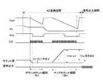
ここでは、単位画素11の具体的な動作については説明を省略するが、周知のように、単位画素11ではリセット動作と転送動作とが行われ、リセット動作では所定の電位にリセットされたときのFD部の電位がリセット成分として単位画素11から列信号線22−1〜22−mに出力され、転送動作では光電変換素子から光電変換による電荷が転送されたときのFD部の電位が信号成分として単位画素11から列信号線22−1〜22−mに出力される。 Here, a description of a specific operation of the
行走査回路13による行走査によってある行iが選択され、その選択行iの単位画素11から列信号線22−1〜22−mへの1回目の読み出し動作が安定した後、DAC151からランプ波形の参照電圧VrefがADC23−1〜23−mの各比較器31に与えられることで、比較器31において列信号線22−1〜22−mの各信号電圧Vxと参照電圧Vrefとの比較動作が行われる。 A row i is selected by row scanning by the
参照電圧Vrefが比較器31に与えられると同時に、タイミング制御回路18からアップ/ダウンカウンタ32に対してクロックCKが与えられることで、当該アップ/ダウンカウンタ32では1回目の読み出し動作時の比較器31での比較時間がダウンカウント動作によって計測される。そして、参照電圧Vrefと列信号線22−1〜22−mの信号電圧Vxとが等しくなったときに比較器31の出力Vcoは“H”レベルから“L”レベルへ反転する。この比較器21の出力Vcoの極性反転を受けて、アップ/ダウンカウンタ32は、ダウンカウント動作を停止して比較器31での1回目の比較期間に応じたカウント値を保持する。 At the same time as the reference voltage Vref is supplied to the comparator 31, the clock CK is supplied from the
この1回目の読み出し動作では、先述したように、単位画素11のリセット成分ΔVが読み出される。このリセット成分ΔV内には、単位画素11毎にばらつく固定パターンノイズがオフセットとして含まれている。しかし、このリセット成分ΔVのばらつきは一般に小さく、またリセットレベルは全画素共通であるため、列信号線22−1〜22−mの信号電圧Vxはおおよそ既知である。したがって、1回目のリセット成分ΔVの読み出し時には、参照電圧Vrefを調整することにより比較期間を短くすることが可能である。本実施形態では、7ビット分のカウント期間(128クロック)でリセット成分ΔVの比較を行っている。 In the first read operation, as described above, the reset component ΔV of the
2回目の読み出し動作では、リセット成分ΔVに加えて、単位画素11毎の入射光量に応じた信号成分Vsig が、1回目のリセット成分ΔVの読み出し動作と同様の動作によって読み出される。すなわち、選択行iの単位画素11から列信号線22−1〜22−mへの2回目の読み出しが安定した後、DAC151から参照電圧VrefがADC23−1〜23−mの各比較器31に与えられることで、比較器31において列信号線22−1〜22−mの各信号電圧Vxと参照電圧Vrefとの比較動作が行われる同時に、この比較器31での2回目の比較時間が、アップ/ダウンカウンタ32において1回目とは逆にアップカウント動作によって計測される。 In the second read operation, in addition to the reset component ΔV, the signal component Vsig corresponding to the amount of incident light for each
このように、アップ/ダウンカウンタ32のカウント動作を1回目にダウンカウント動作とし、2回目にアップカウント動作とすることにより、当該アップ/ダウンカウンタ32内で自動的に(2回目の比較期間)−(1回目の比較期間)の減算処理が行われる。そして、参照電圧Vrefと列信号線22−1〜22−mの信号電圧Vxとが等しくなったときに比較器31の出力Vcoが極性反転し、この極性反転を受けてアップ/ダウンカウンタ32のカウント動作が停止する。その結果、アップ/ダウンカウンタ32には、(2回目の比較期間)−(1回目の比較期間)の減算処理の結果に応じたカウント値が保持される。 As described above, the count operation of the up / down
(2回目の比較期間)−(1回目の比較期間)=(信号成分Vsig +リセット成分ΔV+ADC23のオフセット成分)−(リセット成分ΔV+ADC23のオフセット成分)=(信号成分Vsig )であり、以上2回の読み出し動作とアップ/ダウンカウンタ32での減算処理により、単位画素11毎のばらつきを含んだリセット成分ΔVに加えて、ADC23(23−1〜23−m)毎のオフセット成分も除去されるため、単位画素11毎の入射光量に応じた信号成分Vsig のみを取り出すことができる。ここで、単位画素11毎のばらつきを含んだリセット成分ΔVを除去する処理は、いわゆるCDS(Correlated Double Sampling;相関二重サンプリング)処理である。 (Second comparison period) − (first comparison period) = (signal component Vsig + reset component ΔV + offset component of ADC 23) − (reset component ΔV + offset component of ADC 23) = (signal component Vsig). The offset operation for each ADC 23 (23-1 to 23-m) is removed in addition to the reset component ΔV including the variation for each
2回目の読み出し時には、入射光量に応じた信号成分Vsig が読み出されるので、光量の大小を広い範囲で判定するために参照電圧Vrefを大きく変化させる必要がある。そこで、本実施形態に係るCMOSイメージセンサ10では、信号成分Vsig の読み出しを10ビット分のカウント期間(1024クロック)で比較を行うようにしている。この場合、1回目と2回目との比較ビット数が異なるが、参照電圧Vrefのランプ波形の傾きを1回目と2回目とで同じにすることにより、AD変換の精度を等しくできるため、アップ/ダウンカウンタ32による(2回目の比較期間)−(1回目の比較期間)の減算処理の結果として正しい減算結果が得られる。 At the time of the second reading, the signal component Vsig corresponding to the amount of incident light is read out, so that the reference voltage Vref needs to be changed greatly in order to determine the amount of light in a wide range. Therefore, in the CMOS image sensor 10 according to the present embodiment, the reading of the signal component Vsig is compared in a count period (1024 clocks) for 10 bits. In this case, the number of comparison bits is different between the first time and the second time, but by making the slope of the ramp waveform of the reference voltage Vref the same between the first time and the second time, the AD conversion accuracy can be made equal. A correct subtraction result is obtained as a result of the subtraction process of (second comparison period) − (first comparison period) by the
上述した一連のAD変換動作の終了後、アップ/ダウンカウンタ32にはNビットのデジタル値が保持される。そして、カラム処理部14の各ADC23−1〜23−mでAD変換されたNビットのデジタル値(デジタル信号)は、列走査回路16による列走査により、Nビット幅の水平出力線17を経て順次外部へ出力される。その後、同様の動作が順次行毎に繰り返されることによって2次元画像が生成される。 After completion of the above series of AD conversion operations, the up / down
また、本実施形態に係る列並列ADC搭載のCMOSイメージセンサ10では、ADC23−1〜23−mの各々がメモリ装置34を持っているため、i行目の単位画素11についてAD変換後のデジタル値をメモリ装置34に転送し、水平出力線17から外部へ出力しながら、i+1行目の単位画素11について読み出し動作とアップ/ダウンカウント動作を並行して実行することができる。 Further, in the CMOS image sensor 10 equipped with the column parallel ADC according to the present embodiment, each of the ADCs 23-1 to 23-m has the
次に、AD変換期間の動作と読み出し期間の動作を並行して行う場合について、図3のタイミングチャートを用いて説明する。図3において、VSは1フレーム期間を示す垂直同期信号、HSは1水平走査期間を示す水平同期信号である。 Next, the case where the operation in the AD conversion period and the operation in the reading period are performed in parallel will be described with reference to the timing chart of FIG. In FIG. 3, VS is a vertical synchronizing signal indicating one frame period, and HS is a horizontal synchronizing signal indicating one horizontal scanning period.
図3に示す動作では、アップ/ダウンカウンタ32からメモリ装置34にカウント値を転送した後、アップ/ダウンカウンタ32でカウント動作を実行する前に、アップ/ダウンカウンタ32をリセットする必要がある。アップ/ダウンカウンタ32をリセットしないで、i+1行目のアップダウンカウント動作を実施すると、アップ/ダウンカウンタ32の初期値は、先のi行目のAD変換結果となり、同様の動作を繰り返すとアップ/ダウンカウンタ32にはi行目とi+1行目の加算結果が保持されることになる。 In the operation shown in FIG. 3, after the count value is transferred from the up / down counter 32 to the
続いて、本実施形態に係る列並列ADC搭載のCMOSイメージセンサ10におけるアップ/ダウンカウンタ32での加算処理の動作について、図4のタイミングチャートを用いて説明する。このアップ/ダウンカウンタ32での加算処理は、画素アレイ部12の単位画素11全てから画素情報を読み出す通常フレームレートモードに比べて、単位画素11の露光時間を1/2に設定することによって高フレームレート化を図る高速フレームレートモードの動作時に実行されることになる。 Next, the operation of the addition process in the up / down counter 32 in the CMOS image sensor 10 equipped with the column parallel ADC according to the present embodiment will be described with reference to the timing chart of FIG. The addition processing by the up / down
アップ/ダウンカウンタ32は、Nビットのデジタル値を読み出した後も、そのデジタル値をアップ/ダウンカウンタ32内部に保持することができる。本例では、アップ/ダウンカウンタ32のデータ保持特性を利用して、当該アップ/ダウンカウンタ32において複数の行(本例では、i行とi+1行)間で単位画素11のAD変換値を加算する処理を実現するようにしている。 The up / down counter 32 can hold the digital value in the up / down counter 32 even after reading the N-bit digital value. In this example, by using the data retention characteristic of the up / down
先述したように、i行目の単位画素11の信号を読み出す場合は、i行目の信号成分をVsig 1、i行目のリセット成分をΔV1とすると、アップ/ダウンカウンタ32には、(2回目の比較時間)−(1回目の比較時間)=(Vsig 1+ΔV1)−ΔV1=Vsig 1のデジタル値が保持される。このi行目のAD変換期間が終了した後、アップ/ダウンカウンタ32をリセットしないで、引き続きi+1行目の単位画素11の信号の読み出し動作に移行し、i行目と同様の読み出し動作を繰り返す。 As described above, when reading the signal of the
そして、i+1行目の信号成分をVsig2、2行目のリセット成分をΔV2とすると、i+1行目のAD変換終了時にアップ/ダウンカウンタ32に保持されるデジタル値は、Vsig 1+(Vsig 2+ΔV2)−ΔV2=Vsig 1+Vsig 2となる。このときのアップ/ダウンカウンタ32のデジタル値を、転送スイッチ33によってメモリ装置34に転送した後、水平出力線17を経由して外部へ出力することで、i行目とi+1行目の2行分の単位画素11の信号成分を加算した値Vsig 1+Vsig 2を出力することができる。 When the signal component of the i + 1th row is Vsig2, and the reset component of the second row is ΔV2, the digital value held in the up / down counter 32 at the end of AD conversion of the i + 1th row is
同様の動作を繰り返すことにより、垂直方向(センサ面縦(列)方向)において画素情報を1/2に間引いた画像を得ることができる。その結果、フレームレートを全ての画素情報を読み出す通常フレームレートモード時に比べて2倍に高速化できる。 By repeating the same operation, it is possible to obtain an image in which pixel information is thinned by half in the vertical direction (sensor surface vertical (column) direction). As a result, the frame rate can be increased twice as compared with the normal frame rate mode in which all pixel information is read out.
上述したように、第1実施形態に係る列並列ADC搭載のCMOSイメージセンサ10においては、単位画素11から列信号線22−1〜22−mを経由して出力されるアナログ信号を、例えば画素列毎に設けられたADC23−1〜23−mでデジタル値に変換するとともに、当該デジタル値を垂直方向(列方向)における複数の単位画素11間、例えば2つの単位画素11間で加算して読み出すことにより、次のような作用効果を得ることができる。 As described above, in the CMOS image sensor 10 equipped with the column parallel ADC according to the first embodiment, an analog signal output from the
すなわち、読み出した画素情報数の観点からすれば、画素情報について垂直方向で1/2に間引き読み出し(飛ばし読み出し)を行ったのと同じことになるが、垂直方向における2画素間で画素情報を加算しているため、1つの画素情報についての情報量の観点からすれば2倍となる。したがって、フレームレートを例えば2倍に向上すべく、単位画素11の露光時間を1/2に設定したとしても、AD変換の際にデジタル値を2行分の単位画素間で加算することで、1つの画素情報についての情報量が2倍になるため、通常フレームレートモード時に比べて感度が低下することはない。 That is, from the viewpoint of the number of read pixel information, the pixel information is the same as when the pixel information is thinned and read out in half in the vertical direction (skipping readout), but the pixel information between the two pixels in the vertical direction is changed. Since the addition is performed, it is doubled from the viewpoint of the amount of information about one pixel information. Therefore, even if the exposure time of the
すなわち、単位画素11の露光時間を短縮したとしても、結果として1つの画素情報の情報量が減ることはないため、感度低下を招くことなく、高フレームレート化を実現できる。しかも、ADC23−1〜23−mにアップ/ダウンカウンタ32を内蔵し、当該アップ/ダウンカウンタ32によって加算処理を行うようにしているため、チップ19の外部のメモリ装置を使用したり、あるいは列並列ADCとして追加回路を使ったりしなくても、高精度の加算演算を実現できる。 That is, even if the exposure time of the
なお、上記第1実施形態では、アップ/ダウンカウンタ32を用いて加算処理を行う構成としたが、単に加算処理を行うだけであれば、アップ/ダウンカウンタ32に代えて単なるカウンタを用いることによっても実現できる。ただし、アップ/ダウンカウンタ32を用いることで、単位画素11の信号成分Vsig からリセット成分ΔVを除去するデジタルCDS処理を行いながら、加算処理を行うことができるという利点がある。同様に処理は、デジタル演算処理を行う演算手段を用いることによっても実現できる。 In the first embodiment, the addition process is performed using the up / down
また、上記第1実施形態では、2行間での画素加算を例に挙げて説明したが、2行加算のみならず、複数行に亘って画素加算を行うことも可能である。このとき、加算する行数をM行とすると、画像データ量を1/Mに圧縮することができる。 In the first embodiment, pixel addition between two rows has been described as an example, but it is also possible to perform pixel addition not only over two rows but also over a plurality of rows. At this time, if the number of lines to be added is M, the amount of image data can be compressed to 1 / M.
さらに、上記第1実施形態では、画像データ量を1/Mに圧縮するに際して、データ出力レートを変更することによってフレームレートをM倍にするとしたが、AD変換期間を1/Mに短縮することによってデータ出力レートを変更せずにフレームレートをM倍にすることも可能である。すなわち、第1実施形態に係るCMOSイメージセンサ10の場合と同様に、アップ/ダウンカウンタ32を使って行毎の画素加算を実現することによってデータ量を圧縮することができるが、図5のタイミングチャートに示すように、AD変換期間を1/M、例えば1/2に短縮するとデータ出力レートを変更せずにフレームレートを2倍にすることができる。 Further, in the first embodiment, when the image data amount is compressed to 1 / M, the frame rate is increased by M times by changing the data output rate. However, the AD conversion period is reduced to 1 / M. Thus, the frame rate can be increased M times without changing the data output rate. That is, as in the case of the CMOS image sensor 10 according to the first embodiment, the data amount can be compressed by realizing pixel addition for each row using the up / down
AD変換のビット精度を維持したままAD変換期間を短くできない場合は、図4のタイミングチャートにおいて、アップ/ダウンカウンタ32のアップカウントのデジタルカウント値をN−1ビットまでとする。例えば、10ビットカウントの場合、本来は1024クロック期間で比較を行うが、9ビットカウント、即ち512クロック期間に削減する。このとき、DAC151で生成される参照電圧(ランプ波形)Vrefの時間変化の割合は同一とする。これは、AD変換のビット精度は変化しないことを意味する。 If the AD conversion period cannot be shortened while maintaining the bit accuracy of AD conversion, the digital count value of the up count of the up / down
フレームレートが2倍になると、単位画素当りの蓄積時間は1/2となり、信号振幅も1/2となるためS/Nが低下する。第1実施形態に係るCMOSイメージセンサ10における加算演算を実施すると、2行分の画素加算を実行した後のデジタル値はVsig 1+Vsig 2となり、フレームレートが2倍になった場合でも信号振幅は(Vsig 1+Vsig 2)/2≒Vsig 1となり、信号振幅の変化が少ないためS/Nも劣化しない。 When the frame rate is doubled, the accumulation time per unit pixel is halved and the signal amplitude is also halved, so the S / N is reduced. When the addition operation in the CMOS image sensor 10 according to the first embodiment is performed, the digital value after performing the pixel addition for two rows is
同様に、M行加算を実行してAD変換期間を1/Mに削減した場合フレームレートがM倍となる。このとき、NビットのAD変換のビット精度をN−Mビットに低減することにより、S/Nを劣化させることなく、フレームレートを向上させることができる。 Similarly, when M row addition is performed and the AD conversion period is reduced to 1 / M, the frame rate becomes M times. At this time, the frame rate can be improved without degrading the S / N by reducing the bit precision of N-bit AD conversion to NM bits.
[第2実施形態]
図6は、本発明の第2実施形態に係る列並列ADC搭載CMOSイメージセンサの構成を示すブロック図である。図7に、本実施形態に係るCMOSイメージセンサの動作説明に供するタイミングチャートを示す。[Second Embodiment]
FIG. 6 is a block diagram showing a configuration of a column parallel ADC-mounted CMOS image sensor according to the second embodiment of the present invention. FIG. 7 is a timing chart for explaining the operation of the CMOS image sensor according to this embodiment.
本実施形態に係る列並列ADC搭載CMOSイメージセンサ50は、図1に示した第1実施形態に係る列並列ADC搭載CMOSイメージセンサ10と、基本的な構成については同じであるが、行走査回路13Aが任意の行制御線21−i(21−1〜21−n)を選択できるアドレスデコーダによって構成されている点で相違している。このアドレスデコーダからなる行走査回路13Aによれば、行制御線21−1〜21−nの選択を、例えば図7に示すように、1行目、3行目、2行目、4行目、…の順に行うことができる。 The column parallel ADC mounted CMOS image sensor 50 according to the present embodiment has the same basic configuration as the column parallel ADC mounted CMOS image sensor 10 according to the first embodiment shown in FIG. 13A is different in that it is constituted by an address decoder capable of selecting an arbitrary row control line 21-i (21-1 to 21-n). According to the
このような行走査を実現できることにより、第1実施形態に係るCMOSイメージセンサ10の場合と同様に、例えば2行単位で加算演算を行うものとすると、1行目の行制御線21−1上の画素11−11と3行目の行制御線21−3上の画素11−31、1行目の行制御線21−1上の画素11−12と3行目の行制御線21−3上の画素11−32、…というように、1行目の画素11−11,11−12,11−13,…と、3行目の画素11−31,11−32,11−33,…との画素加算が可能となる。 By realizing such row scanning, as in the case of the CMOS image sensor 10 according to the first embodiment, for example, when the addition operation is performed in units of two rows, on the row control line 21-1 of the first row. The pixel 11-11 on the third row, the pixel 11-31 on the third row control line 21-3, the pixel 11-12 on the first row control line 21-1, and the third row control line 21-3. The upper pixels 11-32,..., The first row pixels 11-11, 11-12, 11-13,... And the third row pixels 11-31, 11-32, 11-33,. And pixel addition can be performed.
同様にして、2行目の行制御線21−2上の画素11−21と4行目の行制御線21−4上の画素11−41、2行目の行制御線21−2上の画素11−22と4行目の行制御線21−4上の画素11−42、…というように、2行目の画素11−21,11−22,11−23,…と、4行目の画素11−41,11−42,11−43,…との画素加算が可能になる。すなわち、奇数行同士および偶数行同士での画素加算を実現できる。 Similarly, the pixel 11-21 on the second row control line 21-2, the pixel 11-41 on the fourth row control line 21-4, and the second row control line 21-2. The pixel 11-22, the pixel 11-42 on the fourth row control line 21-4,..., The second row of pixels 11-21, 11-22, 11-23,. Pixel addition with the other pixels 11-41, 11-42, 11-43,. That is, pixel addition between odd rows and even rows can be realized.
ここで、画素アレイ部12上には、図6に示すベイヤ配列のカラーフィルタが配されているものとする。このカラーフィルタの場合、同一行の画素には、G(Green)、R(Red)またはB(Blue)、Gのカラーフィルタが配置されることになる。 Here, it is assumed that a Bayer array color filter shown in FIG. 6 is arranged on the pixel array unit 12. In the case of this color filter, G (Green), R (Red), B (Blue), and G color filters are arranged in pixels in the same row.
このベイヤ配列のカラーフィルタを有するCMOSイメージセンサでは、第1実施形態に係るCMOSイメージセンサ10の場合のように、行制御線21−1〜21−nを順番に選択していくと、異なるカラーフィルタ要素を持つ画素同士の加算となるため混色を起す。これに対して、本実施形態に係るCMOSイメージセンサ50においては、奇数行同士および偶数行同士での画素加算を行うことができることにより、同色同士の加算演算を行うことができるため、画素加算に伴う混色が発生することはない。 In the CMOS image sensor having this Bayer array color filter, when the row control lines 21-1 to 21-n are sequentially selected as in the CMOS image sensor 10 according to the first embodiment, different colors are obtained. Since it is the addition of pixels having filter elements, color mixing occurs. On the other hand, in the CMOS image sensor 50 according to the present embodiment, pixel addition can be performed between odd-numbered rows and even-numbered rows, so that addition operations between the same colors can be performed. The accompanying color mixture does not occur.
[第3実施形態]
図8は、本発明の第3実施形態に係る列並列ADC搭載CMOSイメージセンサの構成を示すブロック図であり、図中、図1と同等部分には同一符号を付して示している。[Third Embodiment]
FIG. 8 is a block diagram showing a configuration of a column parallel ADC-mounted CMOS image sensor according to the third embodiment of the present invention. In FIG. 8, the same parts as those in FIG.
本実施形態に係る列並列ADC搭載CMOSイメージセンサ60は、図1に示した第1実施形態に係る列並列ADC搭載CMOSイメージセンサ10と、基本的な構成については同じであるが、以下の点で相違している。 The column parallel ADC-mounted CMOS image sensor 60 according to the present embodiment has the same basic configuration as the column parallel ADC-mounted CMOS image sensor 10 according to the first embodiment shown in FIG. Is different.
すなわち、奇数列の列信号線22−1,22−3,…に接続されたADC23−1,23−3,…の各出力は、Nビット幅の水平出力線17−1を通して出力される。また、偶数列の列信号線22−2,22−4,…に接続されたADC23−2,23−4,…の各出力は、Nビット幅の水平出力線17−2を通して出力される。そして、水平出力線17−1を通して出力される奇数列のデジタル信号と、水平出力線17−2を通して出力される奇数列のデジタル信号は、Nビットのデジタル加算器61で加算処理される。 That is, the outputs of the ADCs 23-1, 23-3,... Connected to the odd-numbered column signal lines 22-1, 23-3,... Are output through the N-bit width horizontal output line 17-1. Further, the outputs of the ADCs 23-2, 23-4,... Connected to the even-numbered column signal lines 22-2, 22-4,... Are output through N-bit horizontal output lines 17-2. The odd column digital signal output through the horizontal output line 17-1 and the odd column digital signal output through the horizontal output line 17-2 are added by the N-bit
上記構成の本実施形態に係るCMOSイメージセンサ60では、アップ/ダウンカウンタ32のカウント結果を、メモリ装置34に転送して保持する構成を採っているため、アップ/ダウンカウンタ32のカウント動作と、メモリ装置34からのカウント結果の水平出力線17−1,17−2への読み出し動作とを独立して制御可能である。したがって、アップ/ダウンカウンタ32のカウント動作を行いながら、偶数列、奇数列のカウント値をメモリ装置34からから読み出してデジタル加算器61で加算することが可能となり、結果として、2列間における画素の加算演算を実現することができる。 The CMOS image sensor 60 according to the present embodiment having the above-described configuration employs a configuration in which the count result of the up / down
さらに、本実施形態に係るCMOSイメージセンサ60における列間の加算動作と、第1実施形態に係るCMOSイメージセンサ10における行間の加算動作とを組み合わせることにより、2行2列の加算演算を実現することが可能となる。 Further, by adding the addition operation between columns in the CMOS image sensor 60 according to the present embodiment and the addition operation between rows in the CMOS image sensor 10 according to the first embodiment, an addition operation of 2 rows and 2 columns is realized. It becomes possible.
次に、上記構成の第3実施形態に係るCMOSイメージセンサ60の動作について、図9のタイミングチャートを用いて説明する。 Next, the operation of the CMOS image sensor 60 according to the third embodiment having the above configuration will be described with reference to the timing chart of FIG.
画素アレイ部11の各単位画素11から行単位で信号を読み出し、ADC23−1,23−2,…のアップ/ダウンカウンタ32でカウント動作を行うまでの動作は、第1実施形態に係るCMOSイメージセンサ10の場合と同様であり、x行(x行は1行〜m−1行の任意の行数),x+1行の各デジタルカウント値をアップ/ダウンカウンタ32で加算する動作は、第2実施形態に係るCMOSイメージセンサ50の場合と同様である。 The operation from reading out signals in units of rows from the
上記加算動作後、その加算結果を列ごとにメモリ装置34に転送し、水平出力線17−1,17−2を通して奇数列の加算結果と偶数列の加算結果とをデジタル加算器31に入力させる。このとき、列走査回路16から出力される制御信号M1,M2,M3,…は、M1とM2、M3とM4,…という組み合わせで同時に出力される。これにより、メモリ装置34に保持されているデジタル値(加算結果)が、2列毎に水平信号線17−1,17−2に同時に出力される。 After the addition operation, the addition result is transferred to the
図9のタイミングチャートにおいて、信号出力Aには奇数列の加算結果が、信号出力Bには偶数列の加算結果が出力されている。具体的には、信号出力Aの先頭の信号として画素11−11と画素11−12の加算結果が出力され、信号出力Bの先頭の信号として画素11−21と画素11−22の加算結果が出力される。その結果、デジタル加算器61の先頭出力として、画素11−11,11−12,11−21,11−22の4画素の加算結果が出力される。 In the timing chart of FIG. 9, the addition result of the odd number columns is output to the signal output A, and the addition result of the even number columns is output to the signal output B. Specifically, the addition result of the pixels 11-11 and 11-12 is output as the head signal of the signal output A, and the addition result of the pixels 11-21 and 11-22 is output as the head signal of the signal output B. Is output. As a result, the addition result of the four pixels 11-11, 11-12, 11-21, and 11-22 is output as the head output of the
上述したことから明らかなように、本実施形態に係るCMOSイメージセンサ60によれば、第2実施形態に係るCMOSイメージセンサ50の場合と同様に、AD変換のビット精度を低減し、AD変換期間を1/4に短縮することで、フレームレートを4倍にし、かつ感度を一定に保つことができる。 As is clear from the above, according to the CMOS image sensor 60 according to the present embodiment, the bit accuracy of AD conversion is reduced and the AD conversion period is reduced as in the case of the CMOS image sensor 50 according to the second embodiment. By shortening to 1/4, the frame rate can be quadrupled and the sensitivity can be kept constant.
[第4実施形態]
図10は、本発明の第4実施形態に係る列並列ADC搭載CMOSイメージセンサの構成を示すブロック図であり、図中、図1と同等部分には同一符号を付して示している。[Fourth Embodiment]
FIG. 10 is a block diagram showing a configuration of a column parallel ADC mounted CMOS image sensor according to the fourth embodiment of the present invention. In FIG. 10, the same parts as those in FIG.
先述した第1,第2,第3実施形態に係る列並列ADC搭載CMOSイメージセンサ10,50,60では、画素アレイ部12の上下方向(列方向)の一方側、例えば下側にのみカラム処理部14、参照電圧供給部15、列走査回路16および水平出力線17(17−1,17−2)を配する構成を採っていた。 In the column-parallel ADC-mounted CMOS image sensors 10, 50, 60 according to the first, second, and third embodiments described above, column processing is performed only on one side of the pixel array unit 12 in the vertical direction (column direction), for example, the lower side. The configuration in which the unit 14, the reference
これに対して、本実施形態に係る列並列ADC搭載CMOSイメージセンサ70では、画素アレイ部12の上下方向の両側に、即ち画素アレイ部12を挟んで各々一対ずつのカラム処理部14A,14B、参照電圧供給部15A,15B、列走査回路16A,16Bおよび水平出力線17A,17Bを配するとともに、画素アレイ部12とカラム処理部14A,14Bとの間に選択スイッチ71A,71Bを設けた構成を採っている。 On the other hand, in the CMOS image sensor 70 with column-parallel ADC according to the present embodiment, a pair of
各々一対ずつ設けられたカラム処理部14A,14B、参照電圧供給部15A,15Bおよび列走査回路16A,16Bは、第1実施形態に係るCMOSイメージセンサ10におけるカラム処理部14、参照電圧供給部15および列走査回路16Aと全く同じ構成を有している。 The
水平出力線17A,17Bは各々Nビットの信号線であり、カラム処理部14A,14Bから出力されるNビットのデジタル信号をNビットのデジタル加算器72に伝送する。デジタル加算器72は、水平出力線17A,17Bを通してカラム処理部14A,14Bから出力されるデジタル信号を加算処理する。 The
選択スイッチ71A,71Bは、相補的に動作することで、隣接する例えば2本の列信号線の一方をカラム処理部14Aに接続したとき他方をカラム処理部14Bに接続し、一方をカラム処理部14Bに接続したとき他方をカラム処理部14Aに接続する。 The selection switches 71A and 71B operate in a complementary manner so that, for example, when one of two adjacent column signal lines is connected to the
具体的には、選択スイッチ71A,71Vは、各一方の固定接点aが列信号線22−2の両端に、各他方の固定接点bが列信号線22−3の両端にそれぞれ接続され、各可動接点cがADC23A−2とADC23B−1にそれぞれ接続されている。そして、選択スイッチ71Aの可動接点cが一方の固定接点aに接続されるときは、選択スイッチ71Bの可動接点cが他方の固定接点bに接続され、選択スイッチ71Aの可動接点cが他方の固定接点bに接続されるときは、選択スイッチ71Bの可動接点cが一方の固定接点aに接続されることになる。 Specifically, each of the selection switches 71A and 71V has one fixed contact a connected to both ends of the column signal line 22-2 and each other fixed contact b connected to both ends of the column signal line 22-3. The movable contact c is connected to the
図10には、図面の簡略化のために、列信号線22−2と列信号線22−3との間に接続された選択スイッチ71A,71Bのみを図示したが、これら選択スイッチ71A,71Bは、2列目から隣り合う2本の列信号線を単位として2列おきに設けられることになる。 FIG. 10 shows only the selection switches 71A and 71B connected between the column signal line 22-2 and the column signal line 22-3 for simplification of the drawing, but these
上記構成の本実施形態に係る列並列ADC搭載CMOSイメージセンサ70において、選択スイッチ71Aの可動接点cが固定接点aに接続され、選択スイッチ71Bの可動接点cが固定接点bに接続されたときは、1列目と2列目、5列目と6列目、…の画素のアナログ信号がカラム処理部14A側に、3列目と4列目、7列目と8列目、…の画素の信号がカラム処理部14B側にそれぞれ読み出され、それぞれの比較器31A,31Bおよびアップ/ダウンカウンタ32A,32Bでデジタル信号に変換され、かつメモリ装置34A,34Bに記憶される。このときの等価回路を図11に示す。 In the column-parallel ADC-equipped CMOS image sensor 70 according to the present embodiment having the above configuration, when the movable contact c of the
図12のタイミングチャートに示すように、列走査回路16Aからは制御信号Ma1,Ma2,…が、列走査回路16Bからは制御信号Mb1,Mb2,…がそれぞれ同じタイミングで順に出力される。そして、先ず、制御信号Ma1,Mb1によってADC23A−1,23B−1の各メモリ装置34に格納されている1列目と3列目の各画素のデジタル値が同時に水平出力線17A,17Bに読み出され、次いで制御信号Ma2,Mb2によってADC23A−2,23B−2の各メモリ装置34に格納されている2列目と4列目の各画素のデジタル値が同時に水平出力線17A,17Bに読み出され、以降、同様の動作が順次繰り返される。 As shown in the timing chart of FIG. 12, the
その結果、デジタル加算器72においては、1列目と3列目の各画素のデジタル値が加算され、次いで2列目と4列目の各画素のデジタル値が加算され、…という具合に、奇数列同士および偶数列同士での2列間の画素加算が行われる。このように、奇数列同士および偶数列同士での画素加算を行うことで、図11に示すように、カラーフィルタがベイヤ配列の場合、同色同士の加算演算を行うことができるため、画素加算に伴う混色が発生することはない。 As a result, the
また、本実施形態に係るCMOSイメージセンサ70における2列間の加算動作と、第2実施形態に係るCMOSイメージセンサ50における2行間の加算動作とを組み合わせることにより、列間および行間の双方において同色同士の加算演算を行うことができるため、画素加算に伴う混色を生ずることなく、2行2列の加算演算を実現することが可能となるととともに、フレームレートを4倍にし、かつ感度を一定に保つことができる。 In addition, by combining the addition operation between two columns in the CMOS image sensor 70 according to the present embodiment and the addition operation between two rows in the CMOS image sensor 50 according to the second embodiment, the same color can be obtained both between the columns and between the rows. Since it is possible to perform an addition operation between each other, it is possible to realize an addition operation of 2 rows and 2 columns without causing color mixture due to pixel addition, and to quadruple the frame rate and to make the sensitivity constant. Can keep.
一方、図10において、選択スイッチ71Aの可動接点cが固定接点bに接続され、選択スイッチ71Bの可動接点cが固定接点aに接続されたときは、1列目と3列目、5列目と7列目、…の画素のアナログ信号がカラム処理部14A側に、2列目と4列目、6列目と8列目、…の画素の信号がカラム処理部14B側にそれぞれ読み出され、それぞれの比較器31A,31Bおよびアップ/ダウンカウンタ32A,32Bでデジタル信号に変換され、かつメモリ装置34A,34Bに記憶される。このときの等価回路を図13に示す。 On the other hand, in FIG. 10, when the movable contact c of the
列走査回路16Aからは制御信号Ma1,Ma2,…が、列走査回路16Bからは制御信号Mb1,Mb2,…がそれぞれ同じタイミングで順に出力されることから、先ず、制御信号Ma1,Mb1によってADC23A−1,23B−1の各メモリ装置34に格納されている1列目と2列目の各画素のデジタル値が同時に水平出力線17A,17Bに読み出され、次いで制御信号Ma2,Mb2によってADC23A−2,23B−2の各メモリ装置34に格納されている3列目と4列目の各画素のデジタル値が同時に水平出力線17A,17Bに読み出され、以降、同様の動作が順次繰り返される。 Since the
その結果、デジタル加算器72においては、1列目と2列目の各画素のデジタル値が加算され、次いで3列目と4列目の各画素のデジタル値が加算され、…という具合に、隣り合う(連続する)2列間での画素加算が行われる。このような隣り合う2列間での画素加算は、同一センサ上に同一のカラーフィルタ(Rのみ/Gのみ/Bのみ)が形成されている三板式のイメージセンサでの画素加算に対応できる。 As a result, the
また、本実施形態に係るCMOSイメージセンサ70における2列間の加算動作と、第1実施形態に係るCMOSイメージセンサ10における2行間の加算動作とを組み合わせることで、2行2列の加算演算を実現することが可能となるととともに、フレームレートを4倍にし、かつ感度を一定に保つことができる。 Further, the addition operation between two columns in the CMOS image sensor 70 according to the present embodiment and the addition operation between two rows in the CMOS image sensor 10 according to the first embodiment are combined to perform an addition operation of two rows and two columns. In addition to being able to be realized, the frame rate can be quadrupled and the sensitivity can be kept constant.
上述したように、本実施形態に係るCMOSイメージセンサ70によれば、画素アレイ部12を挟んでカラム処理部14A,14Bを配するとともに、画素アレイ部12とカラム処理部14A,14Bとの間に選択スイッチ71A,71Bを設けたことにより、当該選択スイッチ71A,71Bの作用によって画素加算する列の組み合わせを任意に選択することができるため、同一の回路構成により、ベイヤ配列のような単板式のイメージセンサでも、三板式のイメージセンサでも画素加算を実現することができる。 As described above, according to the CMOS image sensor 70 according to the present embodiment, the
なお、本実施形態では、1対のカラム処理部14A,14Bに対応して1本ずつ水平出力線17A,17Bを設けるとしたが、第3実施形態の場合と同様にして、これら水平出力線17A,17Bを複数本、例えば2本ずつ設けるとともに、列走査回路16A,16Bからは2つの制御信号Mを単位として同時に出力するようにすることで、4列間で画素加算を実現することができる。 In the present embodiment, the
また、本実施形態では、カラム処理部、参照電圧供給部、列走査回路、水平出力線および選択スイッチを一対ずつ設けることによって2列間での画素加算を行うとしたが、カラム処理部、参照電圧供給部、列走査回路、水平出力線および選択スイッチを3つ以上ずつ設けることも可能であり、これによれば、3以上の列間での画素加算を行うことが可能になる。 In this embodiment, pixel addition between two columns is performed by providing a pair of a column processing unit, a reference voltage supply unit, a column scanning circuit, a horizontal output line, and a selection switch. Three or more voltage supply units, column scanning circuits, horizontal output lines, and selection switches can be provided. According to this, pixel addition can be performed between three or more columns.
[第5実施形態]
図14は、本発明の第5実施形態に係る列並列ADC搭載CMOSイメージセンサの構成を示すブロック図であり、図中、図8と同等部分には同一符号を付して示している。[Fifth Embodiment]
FIG. 14 is a block diagram showing a configuration of a column-parallel ADC-mounted CMOS image sensor according to the fifth embodiment of the present invention. In FIG. 14, the same parts as those in FIG.
本実施形態に係る列並列ADC搭載CMOSイメージセンサ80は、図8に示した第3実施形態に係る列並列ADC搭載CMOSイメージセンサ60と、基本的な構成については同じであるが、以下の点で相違している。 The column parallel ADC mounted CMOS image sensor 80 according to the present embodiment is the same in basic configuration as the column parallel ADC mounted CMOS image sensor 60 according to the third embodiment shown in FIG. Is different.
すなわち、第3実施形態に係る列並列ADC搭載CMOSイメージセンサ60では、奇数列同士、偶数列同士での画素加算を実現可能にしているのに対して、本実施形態に係る列並列ADC搭載CMOSイメージセンサ80では、画素アレイ部12とカラム処理部14との間に選択スイッチ81を設け、この選択スイッチ81の作用により、画素加算する列の組み合わせを任意に切り替え可能としている。 That is, in the CMOS image sensor 60 with column-parallel ADC according to the third embodiment, pixel addition between odd-numbered columns and even-numbered columns can be realized, whereas the column-parallel ADC-mounted CMOS according to the present embodiment. In the image sensor 80, a
選択スイッチ81は、互いに連動する2つのスイッチ81A,81Bによって構成されている。スイッチ81Aは、一方の固定接点a1が2列目の列信号線22−2に、他方の固定接点b1が3列目の列信号線22−3に、可動接点c1が2列目のADC23−2にそれぞれ接続されている。スイッチ81Bは、一方の固定接点a2が3列目の列信号線22−3に、他方の固定接点b2が2列目の列信号線22−2に、可動接点c2が3列目のADC23−3にそれぞれ接続されている。 The
図14には、図面の簡略化のために、列信号線22−2と列信号線22−3との間に接続された選択スイッチ81のみを図示したが、この選択スイッチ81は、2列目から隣り合う2本の列信号線を単位として2列おきに設けられることになる。 For simplification of the drawing, FIG. 14 shows only the
上記構成の本実施形態に係る列並列ADC搭載CMOSイメージセンサ80において、選択スイッチ81の可動接点c1,c2が固定接点a1,a2に接続されたときは、1列目、2列目、3列目、4列目…の画素のアナログ信号が、ADC23−1,23−2,23−3,23−4,…でデジタル信号に変換されかつ保持される。 In the column parallel ADC mounted CMOS image sensor 80 according to the present embodiment having the above configuration, when the movable contacts c1 and c2 of the
その後、第3実施形態に係る列並列ADC搭載CMOSイメージセンサ60の場合と同様にして、列走査回路16から制御信号M1,M2,M3,M4,…が、M1とM2、M3とM4,…という組み合わせで同時に出力されることにより、メモリ装置34に保持されているデジタル値が、2列毎に水平信号線17−1,17−2に同時に出力される。そして、水平出力線17−1を通して出力されるデジタル値と、水平出力線17−2を通して出力されるデジタル値とが、Nビットのデジタル加算器61で加算処理される。 Thereafter, in the same manner as in the column parallel ADC-mounted CMOS image sensor 60 according to the third embodiment, the control signals M1, M2, M3, M4,... From the
その結果、デジタル加算器72においては、1列目と2列目の各画素のデジタル値が加算され、次いで3列目と4列目の各画素のデジタル値が加算され、…という具合に、隣り合う(連続する)2列間での画素加算が行われる。このような隣り合う2列間での画素加算は、同一センサ上に同一のカラーフィルタ(Rのみ/Gのみ/Bのみ)が形成されている三板式のイメージセンサでの画素加算に対応できる。 As a result, the
また、本実施形態に係るCMOSイメージセンサ80における2列間の加算動作と、第1実施形態に係るCMOSイメージセンサ10における2行間の加算動作とを組み合わせることで、2行2列の加算演算を実現することが可能となるととともに、フレームレートを4倍にし、かつ感度を一定に保つことができる。 Further, by adding the addition operation between two columns in the CMOS image sensor 80 according to the present embodiment and the addition operation between two rows in the CMOS image sensor 10 according to the first embodiment, an addition operation of two rows and two columns is performed. In addition to being able to be realized, the frame rate can be quadrupled and the sensitivity can be kept constant.
一方、選択スイッチ81の可動接点c1,c2が固定接点b1,b2に接続されたときは、1列目、3列目、…の画素のアナログ信号が、奇数列のADC23−1,23−3,…でデジタル信号に変換されかつ保持される。また、2列目、4列目、…の画素のアナログ信号が、偶数列のADC23−2,23−4,…でデジタル信号に変換されかつ保持される。 On the other hand, when the movable contacts c1 and c2 of the
その後、第3実施形態に係る列並列ADC搭載CMOSイメージセンサ60の場合と同様にして、奇数列のADC23−1,23−3,…の各出力がNビット幅の水平出力線17−1を通して出力され、偶数列のADC23−2,23−4,…の各出力がNビット幅の水平出力線17−2を通して出力される。そして、水平出力線17−1を通して出力される奇数列のデジタル信号と、水平出力線17−2を通して出力される奇数列のデジタル信号は、Nビットのデジタル加算器61で加算処理される。 Thereafter, as in the case of the column-parallel ADC-equipped CMOS image sensor 60 according to the third embodiment, the outputs of the odd-numbered ADCs 23-1, 23-3,... Pass through the horizontal output line 17-1 having an N-bit width. The outputs of the even-numbered ADCs 23-2, 23-4,... Are output through an N-bit horizontal output line 17-2. The odd column digital signal output through the horizontal output line 17-1 and the odd column digital signal output through the horizontal output line 17-2 are added by the N-bit
すなわち、上記の動作は、第3実施形態に係る列並列ADC搭載CMOSイメージセンサ60の動作と同じであり、これにより、奇数列同士、偶数列同士での2画素加算が実現される。その結果、カラーフィルタがベイヤ配列の場合、同色同士の加算演算を行うことができるため、画素加算に伴う混色が発生することはない。 That is, the above operation is the same as the operation of the CMOS image sensor 60 with column-parallel ADC according to the third embodiment, and thereby two-pixel addition is realized between odd columns and even columns. As a result, when the color filter is a Bayer array, it is possible to perform an addition operation between the same colors, so that color mixing due to pixel addition does not occur.
また、本実施形態に係るCMOSイメージセンサ70における2列間の加算動作と、第2実施形態に係るCMOSイメージセンサ50における2行間の加算動作とを組み合わせることにより、列間および行間の双方において同色同士の加算演算を行うことができることになるため、画素加算に伴う混色を生ずることなく、2行2列の加算演算を実現することが可能となるととともに、フレームレートを4倍にし、かつ感度を一定に保つことができる。 In addition, by combining the addition operation between two columns in the CMOS image sensor 70 according to the present embodiment and the addition operation between two rows in the CMOS image sensor 50 according to the second embodiment, the same color can be obtained both between the columns and between the rows. Since it is possible to perform an addition operation between each other, it is possible to realize an addition operation of 2 rows and 2 columns without causing color mixing due to pixel addition, and quadruple the frame rate and increase sensitivity. Can be kept constant.
上述したように、本実施形態に係るCMOSイメージセンサ80によれば、画素アレイ部12とカラム処理部14との間に選択スイッチ81を設けたことにより、当該選択スイッチ81の作用によって画素加算する列の組み合わせを任意に選択することができるため、同一の回路構成により、ベイヤ配列のような単板式のイメージセンサでも、三板式のイメージセンサでも画素加算を実現することができる。 As described above, according to the CMOS image sensor 80 according to the present embodiment, the
なお、本実施形態では、水平出力線を2本設けるとともに、選択スイッチ81を2列間に配することで、列間での2画素加算を実現するとしたが、水平出力線を3本以上設けるとともに、選択スイッチ81を3列以上の列間に配することで、列間での3画素以上の画素加算を実現することも可能である。 In the present embodiment, two horizontal output lines are provided, and the
10,50,60,70,80…列並列ADC搭載CMOSイメージセンサ、11…単位画素、12・画素アレイ部、13…行走査回路、14(14A,14B)…カラム処理部、15(15A,15B)…参照電圧供給部、16(16A,16B)…列走査回路、17(17−1,17−2,17A,17B)…水平出力線、18…タイミング制御回路、21−1〜21−n…行制御線、22−1〜22−m…列信号線、23−1〜23−m…ADC(アナログ−デジタル変換装置)、31(31A,31B)…比較器、32(32A,32B)…アップ/ダウンカウンタ、33…転送スイッチ、34(34A,34B)…メモリ装置、61,72…Nビットデジタル加算器、71A,71B,81…選択スイッチ DESCRIPTION OF SYMBOLS 10, 50, 60, 70, 80 ... CMOS image sensor with column parallel ADC, 11 ... Unit pixel, 12 pixel array part, 13 ... Row scanning circuit, 14 (14A, 14B) ... Column processing part, 15 (15A, 15B) ... reference voltage supply unit, 16 (16A, 16B) ... column scanning circuit, 17 (17-1, 17-2, 17A, 17B) ... horizontal output line, 18 ... timing control circuit, 21-1 to 21- n: row control lines, 22-1 to 22-m, column signal lines, 23-1 to 23-m, ADC (analog-digital converter), 31 (31A, 31B), comparator, 32 (32A, 32B) ) ... Up / down counter, 33 ... Transfer switch, 34 (34A, 34B) ... Memory device, 61,72 ... N-bit digital adder, 71A, 71B, 81 ... Select switch
Claims (8)
Translated fromJapanese前記画素アレイ部の各単位画素を行毎に選択制御する行走査手段と、
前記行走査手段によって選択制御された行の単位画素から前記列信号線を介して出力されるアナログ信号をデジタル信号に変換し、かつ得られたデジタル信号を複数の単位画素間で加算して出力するアナログ−デジタル変換手段と、
前記アナログ−デジタル変換手段で加算されたデジタル信号の出力制御を行う列走査手段と、
前記列走査手段の制御によって前記アナログ−デジタル変換手段から出力されるデジタル信号を伝送する出力線とを備え、
前記アナログ−デジタル変換手段は、
前記単位画素から出力されるアナログ信号を参照電圧と比較する比較手段と、
前記比較手段での比較動作の開始から比較動作の終了までをカウントするカウント手段とを有し、
前記カウント手段にて前記デジタル信号の加算処理を行う
ことを特徴とする固体撮像装置。A pixel array unit in which unit pixels including photoelectric conversion elements are two-dimensionally arranged in a matrix and a column signal line is wired for each column with respect to the matrix arrangement of the unit pixels;
Row scanning means for selectively controlling each unit pixel of the pixel array section for each row;
An analog signal output via the column signal line from the unit pixel in the row controlled and controlled by the row scanning unit is converted into a digital signal, and the obtained digital signal is added between a plurality of unit pixels and output. Analog-to-digital conversion means
Column scanning means for controlling the output of the digital signal added by the analog-digital conversion means;
An output line for transmitting a digitalsignal output from the analog-to-digital conversion means under the control of the column scanning means,
The analog-digital conversion means includes
Comparison means for comparing an analog signal output from the unit pixel with a reference voltage;
Counting means for counting from the start of the comparison operation in the comparison means until the end of the comparison operation,
A solid-state imaging device,wherein the digital signal is added by the counting means .
ことを特徴とする請求項1記載の固体撮像装置。Thecounting means, the solid-state imaging device according to claim1, I characterized in that a counter which performs an addition process of the digital signal by repeating a counting operation for each analog signal of the plurality of unit pixels.
ことを特徴とする請求項2記載の固体撮像装置。Said counter isan up / down counter, a first output from one of the unit pixels performs a subtraction process by performing down-counting and up-counting for the second analog signal, of the plurality of unit pixels The solid-state imaging device according to claim2 , wherein addition processing is performed by repeating up-counting for each analog signal.
ことを特徴とする請求項1記載の固体撮像装置。The solid-state imaging device according to claim 1, wherein the row scanning unit includes an address decoder that selectively controls each unit pixel of the pixel array unit for each arbitrary row.
ことを特徴とする請求項4記載の固体撮像装置。The analog-to-digital conversion means converts analog signals output from unit pixels of a plurality of rows selected and controlled by the row scanning means into digital signals, and converts the digital signals for the unit pixels arranged in the same column. The solid-state imaging device according to claim4 , wherein addition is performed between the plurality of rows.
ことを特徴とする請求項5記載の固体撮像装置。The solid-state imaging device according to claim5, wherein the analog-to-digital conversion unit adds the digital signals for the unit pixels arranged in the same column independently in odd-numbered rows and even-numbered rows.
前記行走査手段によって選択制御された行の単位画素から前記列信号線を介して出力されるアナログ信号を、前記複数系統のアナログ−デジタル変換手段に列単位で振り分ける選択手段と、
前記複数系統のアナログ−デジタル変換手段から出力されるデジタル信号を加算する加算手段とを有する
ことを特徴とする請求項1記載の固体撮像装置。The analog-digital conversion means is provided with a plurality of systems,
A selection unit that distributes an analog signal output from the unit pixel in the row controlled by the row scanning unit via the column signal line to the plurality of analog-to-digital conversion units in units of columns;
The solid-state imaging device according to claim 1, further comprising an adding unit that adds digital signals output from the analog / digital conversion units of the plurality of systems.
前記行走査手段によって選択制御された行の単位画素から前記列信号線を介して出力されるアナログ信号を、前記列信号線ごとに配された前記アナログ−デジタル変換手段に列単位で振り分ける選択手段と、
前記アナログ−デジタル変換手段から前記出力線によって複数系統に分けて伝送されるデジタル信号を加算する加算手段とを有する
ことを特徴とする請求項1記載の固体撮像装置。The analog-digital conversion means is arranged for each column signal line, and the output line is provided with a plurality of systems for transmitting the digital signal output from the analog-digital conversion means in a plurality of systems. ,
Selection means for distributing an analog signal output from the unit pixel in the row controlled by the row scanning means via the column signal line to the analog-digital conversion means arranged for each column signal line in a column unit. When,
The solid-state imaging device according to claim 1, further comprising an adding unit that adds digital signals transmitted from the analog-to-digital conversion unit in a plurality of systems through the output line.
Priority Applications (16)
| Application Number | Priority Date | Filing Date | Title |
|---|---|---|---|
| JP2004208038AJP4107269B2 (en) | 2004-02-23 | 2004-07-15 | Solid-state imaging device |
| US11/058,851US7623173B2 (en) | 2004-02-23 | 2005-02-16 | Solid-state image pickup device having analog-digital converters configured to sum values of multiple pixels in the array and method for driving the same |
| EP05003683AEP1566959B1 (en) | 2004-02-23 | 2005-02-21 | Solid-state image pickup device and method for driving the same |
| KR1020050014555AKR101141449B1 (en) | 2004-02-23 | 2005-02-22 | Solid-state image pickup device and method for driving the same |
| TW094105484ATWI260162B (en) | 2004-02-23 | 2005-02-23 | Solid-state image pickup sensor and its driving method |
| CN2009100038421ACN101478646B (en) | 2004-02-23 | 2005-02-23 | Solid-state image pickup device and method for driving the same |
| US12/419,077US7710479B2 (en) | 2004-02-23 | 2009-04-06 | Solid-state image pickup device having analog-digital converters configured to sum values of multiple pixels in the array and method for driving the same |
| US12/772,573US7961238B2 (en) | 2004-02-23 | 2010-05-03 | Solid-state image pickup device and method for driving the same in a number of modes |
| US13/094,420US8553122B2 (en) | 2004-02-23 | 2011-04-26 | Solid-state image pickup device |
| US14/023,239US8786746B2 (en) | 2004-02-23 | 2013-09-10 | Solid-state image pickup device and method for driving the same in solid-state imaging pickup device and method for driving the same in a number of modes |
| US14/294,942US9313435B2 (en) | 2004-02-23 | 2014-06-03 | Solid-state image pickup device and method for driving the same |
| US14/957,407US9392200B2 (en) | 2004-02-23 | 2015-12-02 | Solid-state image pickup device and method for driving the same in solid-state imaging pickup device and method for driving the same in a number of modes |
| US15/180,300US9769411B2 (en) | 2004-02-23 | 2016-06-13 | Solid-state image pickup device and method for driving the same in solid-state imaging pickup device and method for driving the same in a number of modes |
| US15/644,539US9942505B2 (en) | 2004-02-23 | 2017-07-07 | Solid-state image pickup device and method for driving the same in solid-state imaging pickup device and method for driving the same in a number of modes |
| US15/893,425US10057531B2 (en) | 2004-02-23 | 2018-02-09 | Solid-state image pickup device and method for driving the same in solid-state imaging pickup device and method for driving the same in a number of modes |
| US16/031,390US10764525B2 (en) | 2004-02-23 | 2018-07-10 | Solid-state image pickup device and method for driving the same in solid-state imaging pickup device and method for driving the same in a number of modes |
Applications Claiming Priority (2)
| Application Number | Priority Date | Filing Date | Title |
|---|---|---|---|
| JP2004045943 | 2004-02-23 | ||
| JP2004208038AJP4107269B2 (en) | 2004-02-23 | 2004-07-15 | Solid-state imaging device |
Related Child Applications (1)
| Application Number | Title | Priority Date | Filing Date |
|---|---|---|---|
| JP2008030227ADivisionJP4453761B2 (en) | 2004-02-23 | 2008-02-12 | Solid-state imaging device and driving method of solid-state imaging device |
Publications (2)
| Publication Number | Publication Date |
|---|---|
| JP2005278135A JP2005278135A (en) | 2005-10-06 |
| JP4107269B2true JP4107269B2 (en) | 2008-06-25 |
Family
ID=34713016
Family Applications (1)
| Application Number | Title | Priority Date | Filing Date |
|---|---|---|---|
| JP2004208038AExpired - LifetimeJP4107269B2 (en) | 2004-02-23 | 2004-07-15 | Solid-state imaging device |
Country Status (5)
| Country | Link |
|---|---|
| US (11) | US7623173B2 (en) |
| EP (1) | EP1566959B1 (en) |
| JP (1) | JP4107269B2 (en) |
| KR (1) | KR101141449B1 (en) |
| TW (1) | TWI260162B (en) |
Cited By (1)
| Publication number | Priority date | Publication date | Assignee | Title |
|---|---|---|---|---|
| US9131177B2 (en) | 2011-12-09 | 2015-09-08 | Panasonic Intellectual Property Management Co., Ltd. | Solid-state imaging device and image capturing apparatus including the same |
Families Citing this family (209)
| Publication number | Priority date | Publication date | Assignee | Title |
|---|---|---|---|---|
| US8169517B2 (en)* | 2001-03-26 | 2012-05-01 | Panavision Imaging Llc | Image sensor ADC and CDS per column with oversampling |
| US7903159B2 (en)* | 2001-03-26 | 2011-03-08 | Panavision Imaging Llc | Image sensor ADC and CDS per column |
| JP4107269B2 (en)* | 2004-02-23 | 2008-06-25 | ソニー株式会社 | Solid-state imaging device |
| JP4584634B2 (en)* | 2004-06-29 | 2010-11-24 | オリンパス株式会社 | Solid-state imaging device |
| JP2006018663A (en)* | 2004-07-02 | 2006-01-19 | Fujitsu Ltd | Current stabilization circuit, current stabilization method, and solid-state imaging device |
| JP4481758B2 (en)* | 2004-07-28 | 2010-06-16 | 株式会社東芝 | Signal processing apparatus and data processing apparatus |
| JP4687155B2 (en)* | 2005-03-09 | 2011-05-25 | ソニー株式会社 | Solid-state imaging device and driving method thereof |
| GB2424781B (en)* | 2005-03-30 | 2007-11-28 | Micron Technology Inc | High density row ram for column parallel CMOS image sensors |
| JP4855704B2 (en)* | 2005-03-31 | 2012-01-18 | 株式会社東芝 | Solid-state imaging device |
| TWI429066B (en) | 2005-06-02 | 2014-03-01 | Sony Corp | Semiconductor image sensor module and manufacturing method thereof |
| US8179296B2 (en)* | 2005-09-30 | 2012-05-15 | The Massachusetts Institute Of Technology | Digital readout method and apparatus |
| JP4765578B2 (en)* | 2005-11-24 | 2011-09-07 | ソニー株式会社 | Solid-state imaging device, driving method thereof, and camera module |
| JP4802767B2 (en)* | 2006-03-06 | 2011-10-26 | ソニー株式会社 | Analog-digital converter, solid-state imaging device using the same, and driving method thereof |
| JP4744343B2 (en)* | 2006-04-10 | 2011-08-10 | ソニー株式会社 | Solid-state imaging device and driving method of solid-state imaging device |
| CN101455070B (en) | 2006-05-22 | 2014-06-11 | 汤姆森特许公司 | Image sensor and method for reading out pixels of the image sensor |
| WO2007146158A1 (en)* | 2006-06-07 | 2007-12-21 | The Trustees Of Columbia University In The City Of New York | Dna sequencing by nanopore using modified nucleotides |
| JP4882545B2 (en)* | 2006-06-28 | 2012-02-22 | ソニー株式会社 | Solid-state imaging device |
| JP2008017090A (en)* | 2006-07-05 | 2008-01-24 | Casio Comput Co Ltd | Imaging apparatus and electronic zoom method |
| KR100803229B1 (en)* | 2006-08-09 | 2008-02-14 | (주) 픽셀플러스 | Image sensor sharing lead-out circuit and how to share lead-out circuit |
| US7755017B2 (en)* | 2006-10-13 | 2010-07-13 | Sony Corporation | Solid-image-pickup device, image-pickup device, and method of driving solid-image-pickup device |
| JP4952498B2 (en)* | 2006-10-13 | 2012-06-13 | ソニー株式会社 | Data processing device, solid-state imaging device, imaging device, electronic device |
| EP2079231B1 (en) | 2006-10-24 | 2014-04-30 | Sony Corporation | Imaging device and reproduction control device |
| US20100226495A1 (en) | 2007-10-29 | 2010-09-09 | Michael Kelly | Digital readout method and apparatus |
| JP4843461B2 (en) | 2006-11-13 | 2011-12-21 | 株式会社東芝 | Solid-state imaging device |
| JP2008136043A (en)* | 2006-11-29 | 2008-06-12 | Sony Corp | Solid-state imaging device and imaging device |
| US8237808B2 (en) | 2007-01-17 | 2012-08-07 | Sony Corporation | Solid state imaging device and imaging apparatus adjusting the spatial positions of pixels after addition by controlling the ratio of weight values during addition |
| JP4674589B2 (en) | 2007-02-05 | 2011-04-20 | ソニー株式会社 | Solid-state imaging device and imaging device |
| JP4325681B2 (en)* | 2007-02-13 | 2009-09-02 | ソニー株式会社 | Solid-state imaging device, imaging device |
| JP4101281B1 (en) | 2007-03-15 | 2008-06-18 | キヤノン株式会社 | Solid-state imaging device and driving method of solid-state imaging device |
| JP5066996B2 (en)* | 2007-04-23 | 2012-11-07 | ソニー株式会社 | Solid-state imaging device, signal processing method for solid-state imaging device, and imaging device |
| JP4389959B2 (en)* | 2007-04-23 | 2009-12-24 | ソニー株式会社 | Solid-state imaging device, signal processing method for solid-state imaging device, and imaging device |
| JP5067011B2 (en)* | 2007-05-18 | 2012-11-07 | ソニー株式会社 | Solid-state imaging device, imaging device, electronic equipment |
| JP2008294913A (en)* | 2007-05-28 | 2008-12-04 | Panasonic Corp | Solid-state imaging device and driving method thereof |
| US7884871B2 (en)* | 2007-06-15 | 2011-02-08 | Aptina Imaging Corporation | Images with high speed digital frame transfer and frame processing |
| US7538702B2 (en)* | 2007-06-15 | 2009-05-26 | Micron Technology, Inc. | Quantizing circuits with variable parameters |
| US7889257B2 (en)* | 2007-07-18 | 2011-02-15 | Mesa Imaging Ag | On-chip time-based digital conversion of pixel outputs |
| US8063976B2 (en)* | 2007-07-24 | 2011-11-22 | Casio Computer Co., Ltd. | Image pick-up apparatus and method of controlling the image pick-up apparatus |
| JP4929090B2 (en)* | 2007-07-26 | 2012-05-09 | パナソニック株式会社 | Solid-state imaging device and driving method thereof |
| JP4951440B2 (en)* | 2007-08-10 | 2012-06-13 | 富士フイルム株式会社 | Imaging apparatus and solid-state imaging device driving method |
| JP4379504B2 (en) | 2007-08-13 | 2009-12-09 | ソニー株式会社 | Solid-state imaging device and camera system |
| KR101377270B1 (en)* | 2007-08-29 | 2014-03-21 | 삼성전자주식회사 | Image sensor having ripple counter and method of operating the image sensor |
| JP4386118B2 (en) | 2007-08-31 | 2009-12-16 | ソニー株式会社 | Imaging circuit |
| JP4853445B2 (en)* | 2007-09-28 | 2012-01-11 | ソニー株式会社 | A / D conversion circuit, solid-state imaging device, and camera system |
| JP2009089085A (en)* | 2007-09-28 | 2009-04-23 | Sony Corp | Solid-state imaging device, driving method thereof, and camera system |
| JP4978795B2 (en) | 2007-09-28 | 2012-07-18 | ソニー株式会社 | Solid-state imaging device, drive control method, and imaging device |
| JP4858388B2 (en) | 2007-09-28 | 2012-01-18 | ソニー株式会社 | Solid-state imaging device, drive control method, and imaging device |
| US7920190B2 (en)* | 2007-10-11 | 2011-04-05 | Aptina Imaging Corporation | Method and apparatus providing column parallel architecture for imagers |
| TWI399088B (en) | 2007-10-12 | 2013-06-11 | Sony Corp | Data processor, solid-state imaging device, imaging device, and electronic device |
| JP2009124514A (en)* | 2007-11-15 | 2009-06-04 | Sony Corp | Solid-state imaging device and camera system |
| JP4900200B2 (en) | 2007-11-15 | 2012-03-21 | ソニー株式会社 | Solid-state imaging device and camera system |
| JP4403435B2 (en) | 2007-11-16 | 2010-01-27 | ソニー株式会社 | Solid-state imaging device, drive control method, and imaging device |
| US7855748B2 (en)* | 2007-12-03 | 2010-12-21 | Altasens, Inc. | Reference voltage generation in imaging sensors |
| JP4661876B2 (en) | 2008-01-18 | 2011-03-30 | ソニー株式会社 | Solid-state imaging device and camera system |
| JP2009206709A (en)* | 2008-02-27 | 2009-09-10 | Sony Corp | Solid-state imaging apparatus, driving method of solid-state imaging apparatus and electronic apparatus |
| JP4442695B2 (en)* | 2008-02-29 | 2010-03-31 | ソニー株式会社 | Solid-state imaging device and camera device |
| JP4661891B2 (en)* | 2008-03-18 | 2011-03-30 | ソニー株式会社 | AD converter, solid-state imaging device, and camera system |
| JP4569647B2 (en)* | 2008-03-18 | 2010-10-27 | ソニー株式会社 | AD converter, AD conversion method, solid-state imaging device, and camera system |
| JP5059669B2 (en)* | 2008-03-26 | 2012-10-24 | オリンパス株式会社 | Solid-state imaging device |
| JP4500862B2 (en) | 2008-04-11 | 2010-07-14 | キヤノン株式会社 | Driving method of solid-state imaging device |
| US8023022B2 (en)* | 2008-05-13 | 2011-09-20 | Olympus Corporation | Solid-state imaging apparatus |
| JP5347341B2 (en)* | 2008-06-06 | 2013-11-20 | ソニー株式会社 | Solid-state imaging device, imaging device, electronic device, AD conversion device, AD conversion method |
| JP5279352B2 (en)* | 2008-06-06 | 2013-09-04 | キヤノン株式会社 | Solid-state imaging device |
| JP5272634B2 (en)* | 2008-06-20 | 2013-08-28 | ソニー株式会社 | Solid-state imaging device, signal processing method for solid-state imaging device, and imaging device |
| JP4725608B2 (en) | 2008-07-03 | 2011-07-13 | ソニー株式会社 | Comparator, comparator calibration method, solid-state imaging device, and camera system |
| JP4661912B2 (en) | 2008-07-18 | 2011-03-30 | ソニー株式会社 | Solid-state imaging device and camera system |
| US8253809B2 (en)* | 2008-08-27 | 2012-08-28 | Sony Corporation | Analog-digital converter, analog-digital conversion method, image pickup device, method of driving the same, and camera |
| JP2010057019A (en)* | 2008-08-29 | 2010-03-11 | Sony Corp | Imaging element, and imaging apparatus |
| JP5435916B2 (en)* | 2008-09-18 | 2014-03-05 | 富士フイルム株式会社 | Electronic endoscope system |
| JP2010081259A (en)* | 2008-09-25 | 2010-04-08 | Panasonic Corp | Solid-state imaging device |
| JP5407264B2 (en)* | 2008-10-09 | 2014-02-05 | ソニー株式会社 | Solid-state imaging device and camera system |
| US20100301398A1 (en)* | 2009-05-29 | 2010-12-02 | Ion Torrent Systems Incorporated | Methods and apparatus for measuring analytes |
| JP2010114550A (en) | 2008-11-05 | 2010-05-20 | Sony Corp | Imaging element, drive method for imaging element and camera |
| JP2010147614A (en)* | 2008-12-16 | 2010-07-01 | Panasonic Corp | Solid-state imaging apparatus and method for driving the same, imaging apparatus |
| JP2010154372A (en)* | 2008-12-25 | 2010-07-08 | Panasonic Corp | Solid-state imaging device, digital camera, and ad conversion method |
| JP4650572B2 (en) | 2009-01-20 | 2011-03-16 | ソニー株式会社 | Image sensor, control method therefor, and camera |
| US8913166B2 (en)* | 2009-01-21 | 2014-12-16 | Canon Kabushiki Kaisha | Solid-state imaging apparatus |
| JP5521345B2 (en)* | 2009-02-12 | 2014-06-11 | 株式会社ニコン | Imaging unit and imaging apparatus |
| KR101621244B1 (en)* | 2009-02-13 | 2016-05-16 | 삼성전자주식회사 | Counter Circuit, Device Including the Same, and Counting Method |
| JP5251592B2 (en) | 2009-02-25 | 2013-07-31 | ソニー株式会社 | Solid-state imaging device, imaging device, semiconductor device |
| KR101365408B1 (en)* | 2009-03-03 | 2014-02-19 | 삼성전자주식회사 | Counter Circuit, Device Including the Same, and Counting Method |
| JP2010212365A (en)* | 2009-03-09 | 2010-09-24 | Sony Corp | Solid-state image pickup device and manufacturing method thereof, and electronic apparatus |
| JP2010251957A (en) | 2009-04-14 | 2010-11-04 | Sony Corp | AD converter, solid-state imaging device, and camera system |
| JP5304410B2 (en) | 2009-04-17 | 2013-10-02 | ソニー株式会社 | AD converter, solid-state imaging device, and camera system |
| JP5359521B2 (en) | 2009-04-24 | 2013-12-04 | ソニー株式会社 | Binary value conversion circuit and method, AD conversion apparatus, solid-state imaging device, and camera system |
| JP5233828B2 (en) | 2009-05-11 | 2013-07-10 | ソニー株式会社 | Solid-state imaging device, driving method of solid-state imaging device, and electronic apparatus |
| JP2010268080A (en) | 2009-05-12 | 2010-11-25 | Canon Inc | Solid-state imaging device |
| KR101597785B1 (en)* | 2009-07-14 | 2016-02-25 | 삼성전자주식회사 | Image sensor and image processing method |
| JP5218309B2 (en)* | 2009-07-14 | 2013-06-26 | ソニー株式会社 | Solid-state imaging device, control method therefor, and camera system |
| US8310580B2 (en) | 2009-07-27 | 2012-11-13 | Sony Corporation | Solid-state imaging device and camera system for suppressing occurrence of quantization vertical streaks |
| JP5251778B2 (en) | 2009-08-03 | 2013-07-31 | ソニー株式会社 | Solid-state imaging device, analog-digital conversion method of solid-state imaging device, and electronic apparatus |
| JP5418073B2 (en)* | 2009-08-28 | 2014-02-19 | ソニー株式会社 | DA converter and solid-state imaging device |
| JP5429547B2 (en)* | 2009-10-02 | 2014-02-26 | ソニー株式会社 | Solid-state imaging device, imaging device, AD conversion method |
| JP5434502B2 (en) | 2009-11-13 | 2014-03-05 | ソニー株式会社 | Solid-state imaging device, driving method thereof, and camera system |
| US8324914B2 (en) | 2010-02-08 | 2012-12-04 | Genia Technologies, Inc. | Systems and methods for characterizing a molecule |
| US9605307B2 (en) | 2010-02-08 | 2017-03-28 | Genia Technologies, Inc. | Systems and methods for forming a nanopore in a lipid bilayer |
| US9678055B2 (en) | 2010-02-08 | 2017-06-13 | Genia Technologies, Inc. | Methods for forming a nanopore in a lipid bilayer |
| JP5493980B2 (en) | 2010-02-19 | 2014-05-14 | ソニー株式会社 | Solid-state imaging device and camera system |
| JP5799531B2 (en) | 2010-04-30 | 2015-10-28 | ソニー株式会社 | A / D converter, A / D conversion method, solid-state imaging device, and camera system |
| JP5631050B2 (en) | 2010-05-10 | 2014-11-26 | キヤノン株式会社 | Solid-state imaging device and camera |
| JP5521758B2 (en) | 2010-05-13 | 2014-06-18 | ソニー株式会社 | Solid-state imaging device and camera system |
| JP2011259407A (en) | 2010-05-13 | 2011-12-22 | Sony Corp | Signal processing circuit, solid state image sensor, and camera system |
| JP5531797B2 (en) | 2010-06-15 | 2014-06-25 | ソニー株式会社 | Solid-state imaging device and camera system |
| JP5609358B2 (en) | 2010-07-20 | 2014-10-22 | ソニー株式会社 | IMAGING DEVICE, CONTROL DEVICE, AND IMAGING DEVICE CONTROL METHOD |
| US8716643B2 (en)* | 2010-09-06 | 2014-05-06 | King Abdulaziz City Science And Technology | Single photon counting image sensor and method |
| JP5664141B2 (en) | 2010-11-08 | 2015-02-04 | ソニー株式会社 | Solid-state imaging device and camera system |
| KR101191916B1 (en)* | 2010-11-17 | 2012-10-17 | 에스케이하이닉스 주식회사 | Image sensing device and method for operating the same |
| JP2012124729A (en)* | 2010-12-09 | 2012-06-28 | Sony Corp | Image pickup device and imaging apparatus |
| WO2012088341A2 (en) | 2010-12-22 | 2012-06-28 | Genia Technologies, Inc. | Nanopore-based single dna molecule characterization, identification and isolation using speed bumps |
| US8962242B2 (en) | 2011-01-24 | 2015-02-24 | Genia Technologies, Inc. | System for detecting electrical properties of a molecular complex |
| US9110478B2 (en) | 2011-01-27 | 2015-08-18 | Genia Technologies, Inc. | Temperature regulation of measurement arrays |
| JP2012191359A (en) | 2011-03-09 | 2012-10-04 | Sony Corp | A/d conversion device, a/d conversion method and program |
| US9052497B2 (en) | 2011-03-10 | 2015-06-09 | King Abdulaziz City For Science And Technology | Computing imaging data using intensity correlation interferometry |
| US9099214B2 (en) | 2011-04-19 | 2015-08-04 | King Abdulaziz City For Science And Technology | Controlling microparticles through a light field having controllable intensity and periodicity of maxima thereof |
| JP2012253624A (en) | 2011-06-03 | 2012-12-20 | Sony Corp | Solid-state imaging device and camera system |
| JP5821300B2 (en) | 2011-06-07 | 2015-11-24 | ソニー株式会社 | Imaging apparatus and imaging method |
| JP5822547B2 (en)* | 2011-06-10 | 2015-11-24 | キヤノン株式会社 | Imaging apparatus and imaging system |
| JP5845140B2 (en) | 2011-06-29 | 2016-01-20 | キヤノン株式会社 | Imaging device and imaging apparatus |
| WO2013006188A1 (en) | 2011-07-01 | 2013-01-10 | Schultz Kenneth I | Methods and apparatus for in-pixel filtering in focal plane arrays |
| JP2013055499A (en) | 2011-09-02 | 2013-03-21 | Sony Corp | Solid state imaging device and camera system |
| JP2013055500A (en) | 2011-09-02 | 2013-03-21 | Sony Corp | Solid state imaging device and camera system |
| JP5862126B2 (en)* | 2011-09-06 | 2016-02-16 | ソニー株式会社 | Imaging device and method, and imaging apparatus |
| JP5858695B2 (en)* | 2011-09-08 | 2016-02-10 | キヤノン株式会社 | Solid-state imaging device and driving method of solid-state imaging device |
| JP5850680B2 (en)* | 2011-09-09 | 2016-02-03 | キヤノン株式会社 | Imaging apparatus and control method thereof |
| JP5935274B2 (en) | 2011-09-22 | 2016-06-15 | ソニー株式会社 | Solid-state imaging device, control method for solid-state imaging device, and control program for solid-state imaging device |
| JP2015039086A (en)* | 2011-12-16 | 2015-02-26 | パナソニック株式会社 | Solid state image pickup device, imaging apparatus |
| JP5979882B2 (en) | 2012-01-13 | 2016-08-31 | キヤノン株式会社 | Solid-state imaging device |
| JP5979896B2 (en)* | 2012-02-09 | 2016-08-31 | キヤノン株式会社 | Solid-state imaging device |
| JP2013168880A (en) | 2012-02-16 | 2013-08-29 | Sony Corp | Comparator, ad converter, solid-state imaging device, camera system, and electronic apparatus |
| JP2013172270A (en) | 2012-02-20 | 2013-09-02 | Sony Corp | Comparator, ad converter, solid-state image pickup device, camera system and electronic apparatus |
| US8986629B2 (en) | 2012-02-27 | 2015-03-24 | Genia Technologies, Inc. | Sensor circuit for controlling, detecting, and measuring a molecular complex |
| JP6151530B2 (en) | 2012-02-29 | 2017-06-21 | 株式会社半導体エネルギー研究所 | Image sensor, camera, and surveillance system |
| EP2822271B1 (en) | 2012-02-29 | 2021-01-13 | Sony Corporation | Column a/d converter, column a/d conversion method, solid imaging device, and camera system |
| JP2013192059A (en) | 2012-03-14 | 2013-09-26 | Sony Corp | Solid-state imaging apparatus, driving method and electronic apparatus |
| KR101934260B1 (en) | 2012-03-19 | 2019-01-03 | 삼성전자 주식회사 | A image sensor |
| FR2989219B1 (en)* | 2012-04-04 | 2015-05-29 | Commissariat Energie Atomique | PROCESSING CIRCUIT OF PIXELS |
| US8830361B2 (en)* | 2012-04-12 | 2014-09-09 | Taiwan Semiconductor Manufacturing Company, Ltd. | Method of reducing column fixed pattern noise |
| JP5841894B2 (en) | 2012-04-25 | 2016-01-13 | ルネサスエレクトロニクス株式会社 | Solid-state imaging device |
| JP5978771B2 (en)* | 2012-05-31 | 2016-08-24 | ソニー株式会社 | Signal processing apparatus and method, imaging device, and imaging apparatus |
| EP2861768A4 (en) | 2012-06-15 | 2016-03-02 | Genia Technologies Inc | Chip set-up and high-accuracy nucleic acid sequencing |
| JP6049332B2 (en) | 2012-07-11 | 2016-12-21 | キヤノン株式会社 | Photoelectric conversion device and imaging system |
| US9036065B1 (en)* | 2012-08-16 | 2015-05-19 | Rambus Inc. | Shared-counter image sensor |
| JP6053398B2 (en)* | 2012-09-03 | 2016-12-27 | キヤノン株式会社 | Imaging device driving method, imaging system driving method, imaging device, and imaging system |
| US9605309B2 (en) | 2012-11-09 | 2017-03-28 | Genia Technologies, Inc. | Nucleic acid sequencing using tags |
| JP2014121060A (en) | 2012-12-19 | 2014-06-30 | Sony Corp | Analog-digital converter, solid state imaging device and electronic apparatus |
| GB201300999D0 (en)* | 2013-01-21 | 2013-03-06 | Cmosis Nv | Analog-to-digital conversation in pixel arrays |
| US9759711B2 (en) | 2013-02-05 | 2017-09-12 | Genia Technologies, Inc. | Nanopore arrays |
| JP6346479B2 (en)* | 2013-05-16 | 2018-06-20 | キヤノン株式会社 | IMAGING DEVICE, IMAGING DEVICE CONTROL METHOD, AND PROGRAM |
| US9551697B2 (en) | 2013-10-17 | 2017-01-24 | Genia Technologies, Inc. | Non-faradaic, capacitively coupled measurement in a nanopore cell array |
| WO2015061509A1 (en) | 2013-10-23 | 2015-04-30 | Genia Technologies, Inc. | High speed molecular sensing with nanopores |
| US9322062B2 (en) | 2013-10-23 | 2016-04-26 | Genia Technologies, Inc. | Process for biosensor well formation |
| KR102210539B1 (en) | 2013-12-26 | 2021-02-01 | 삼성전자주식회사 | correlated double sampling circuit, analog-to digital converter and image sensor including the same |
| JP6224819B2 (en)* | 2014-03-12 | 2017-11-08 | 富士フイルム株式会社 | Endoscope system, processor device for endoscope system, and method for operating endoscope system |
| JP2015216625A (en) | 2014-04-22 | 2015-12-03 | キヤノン株式会社 | Imaging element and imaging apparatus |
| KR20150127923A (en) | 2014-05-07 | 2015-11-18 | 에스케이하이닉스 주식회사 | Image sensing device |
| JP6612056B2 (en)* | 2014-05-16 | 2019-11-27 | 株式会社半導体エネルギー研究所 | Imaging device and monitoring device |
| US10250824B2 (en) | 2014-06-12 | 2019-04-02 | The University Of North Carolina At Chapel Hill | Camera sensor with event token based image capture and reconstruction |
| KR102261595B1 (en) | 2014-09-19 | 2021-06-04 | 삼성전자주식회사 | An image sensor, and an image processing system including the same |
| JP5914612B2 (en)* | 2014-10-08 | 2016-05-11 | キヤノン株式会社 | Solid-state imaging device and camera |
| KR102210513B1 (en)* | 2014-12-11 | 2021-02-02 | 삼성전자주식회사 | Image sensor for performing coupling-free readout, and device having the same |
| US9531979B2 (en)* | 2014-12-30 | 2016-12-27 | Stmicroelectronics (Grenoble 2) Sas | IC image sensor device with twisted pixel lines and related methods |
| WO2016113837A1 (en)* | 2015-01-13 | 2016-07-21 | オリンパス株式会社 | Image-capture device and image-capture system |
| US10306168B2 (en) | 2015-05-04 | 2019-05-28 | Semiconductor Energy Laboratory Co., Ltd. | Semiconductor device, imaging system, and electronic device |
| CN108028898B (en) | 2015-09-16 | 2020-09-04 | 佳能株式会社 | Image Sensors and Camera Equipment |
| WO2017047010A1 (en) | 2015-09-16 | 2017-03-23 | Canon Kabushiki Kaisha | Image sensor and image capturing apparatus |
| CN107135359B (en)* | 2016-02-26 | 2020-04-14 | 上海箩箕技术有限公司 | Image acquisition method of TFT flat-panel image sensor |
| US9955096B2 (en)* | 2016-03-22 | 2018-04-24 | Taiwan Semiconductor Manufacturing Co., Ltd. | System and method for high-speed down-sampled CMOS image sensor readout |
| KR102527110B1 (en)* | 2016-05-23 | 2023-05-03 | 에스케이하이닉스 주식회사 | Analog-digital converting apparatus and operating method |
| JP6701001B2 (en) | 2016-06-22 | 2020-05-27 | キヤノン株式会社 | Imaging device, control method thereof, program, and storage medium |
| US9711231B1 (en)* | 2016-06-24 | 2017-07-18 | Sandisk Technologies Llc | System solution for first read issue using time dependent read voltages |
| JP6792361B2 (en) | 2016-07-20 | 2020-11-25 | キヤノン株式会社 | Imaging device and its control method |
| JP7011240B2 (en)* | 2016-09-08 | 2022-01-26 | ソニーグループ株式会社 | Image sensor and drive method, as well as electronic devices |
| JP6530736B2 (en) | 2016-10-18 | 2019-06-12 | キヤノン株式会社 | Image pickup apparatus and control method thereof |
| US9952944B1 (en) | 2016-10-25 | 2018-04-24 | Sandisk Technologies Llc | First read solution for memory |
| US10262743B2 (en) | 2016-10-25 | 2019-04-16 | Sandisk Technologies Llc | Command sequence for first read solution for memory |
| JP6903417B2 (en) | 2016-11-07 | 2021-07-14 | ソニーセミコンダクタソリューションズ株式会社 | Solid-state image sensor and control method, and electronic equipment |
| CN109906388B (en)* | 2016-11-15 | 2023-03-03 | 深圳帧观德芯科技有限公司 | Image sensor with a plurality of pixels |
| KR102617441B1 (en)* | 2016-12-29 | 2023-12-27 | 에스케이하이닉스 주식회사 | Analog-digital converting apparatus and operating method |
| CN107174268A (en)* | 2017-04-24 | 2017-09-19 | 沈阳东软医疗系统有限公司 | A kind of collecting method and device |
| US10090030B1 (en)* | 2017-04-28 | 2018-10-02 | Hewlett Packard Enterprise Development Lp | Signal conversion using an analog-to-digital converter and reference voltage comparison |
| JP6528819B2 (en)* | 2017-09-01 | 2019-06-12 | 株式会社リコー | PHOTOELECTRIC CONVERSION ELEMENT, IMAGE READING APPARATUS, IMAGE FORMING APPARATUS, AND IMAGE READING METHOD |
| JP7072362B2 (en) | 2017-09-26 | 2022-05-20 | ブリルニクス シンガポール プライベート リミテッド | Solid-state image sensor, solid-state image sensor driving method, and electronic equipment |
| CN109561264B (en) | 2017-09-26 | 2020-12-22 | 普里露尼库斯股份有限公司 | Solid-state imaging device, driving method of solid-state imaging device, and electronic device |
| WO2019078483A1 (en)* | 2017-10-19 | 2019-04-25 | 광주과학기술원 | Compressive sensing image sensor which can improve frame rate, and operating method therefor |
| JP7100439B2 (en) | 2017-10-20 | 2022-07-13 | ブリルニクス シンガポール プライベート リミテッド | Solid-state image sensor, solid-state image sensor driving method, and electronic equipment |
| JP6987603B2 (en) | 2017-10-26 | 2022-01-05 | ブリルニクス シンガポール プライベート リミテッド | Solid-state image sensor, solid-state image sensor driving method, and electronic equipment |
| US10347315B2 (en) | 2017-10-31 | 2019-07-09 | Sandisk Technologies Llc | Group read refresh |
| JP7018293B2 (en) | 2017-11-06 | 2022-02-10 | ブリルニクス シンガポール プライベート リミテッド | Solid-state image sensor, solid-state image sensor driving method, and electronic equipment |
| JP7018294B2 (en) | 2017-11-10 | 2022-02-10 | ブリルニクス シンガポール プライベート リミテッド | Solid-state image sensor, solid-state image sensor driving method, and electronic equipment |
| US10692179B2 (en)* | 2017-11-17 | 2020-06-23 | Semiconductor Components Industries, Llc | Methods and apparatus for signal distribution in an image sensor |
| KR102474449B1 (en)* | 2018-03-07 | 2022-12-06 | 삼성전자주식회사 | Image sensor and electronic system including the same |
| JP6693537B2 (en)* | 2018-04-20 | 2020-05-13 | ソニー株式会社 | Imaging device and imaging device |
| KR102538220B1 (en)* | 2018-10-02 | 2023-06-01 | 삼성전자주식회사 | Image sensing system and operating method of the same |
| JP2020088481A (en)* | 2018-11-19 | 2020-06-04 | ソニーセミコンダクタソリューションズ株式会社 | Solid-state imaging device and imaging device |
| US11360704B2 (en)* | 2018-12-21 | 2022-06-14 | Micron Technology, Inc. | Multiplexed signal development in a memory device |
| JP7341659B2 (en) | 2018-12-25 | 2023-09-11 | ブリルニクス シンガポール プライベート リミテッド | Solid-state imaging device, driving method for solid-state imaging device, and electronic equipment |
| JP7319780B2 (en) | 2019-01-11 | 2023-08-02 | ブリルニクス シンガポール プライベート リミテッド | Solid-state imaging device, driving method for solid-state imaging device, and electronic device |
| JP7338974B2 (en) | 2019-01-11 | 2023-09-05 | ブリルニクス シンガポール プライベート リミテッド | Solid-state imaging device, driving method for solid-state imaging device, and electronic device |
| JP7460345B2 (en) | 2019-09-30 | 2024-04-02 | ブリルニクス シンガポール プライベート リミテッド | Solid-state imaging device, driving method for solid-state imaging device, and electronic device |
| US11297270B2 (en) | 2019-12-26 | 2022-04-05 | Sony Corporation | Readout circuit and method for time-of-flight image sensor |
| JP7638961B2 (en) | 2020-03-24 | 2025-03-04 | ソニーセミコンダクタソリューションズ株式会社 | Imaging device |
| JP2022071317A (en) | 2020-10-28 | 2022-05-16 | ブリルニクス シンガポール プライベート リミテッド | Solid-state imaging device, method for driving solid-state imaging device, and electronic apparatus |
| JP7656469B2 (en) | 2021-04-05 | 2025-04-03 | ブリルニクス シンガポール プライベート リミテッド | Solid-state imaging device, driving method for solid-state imaging device, and electronic device |
| US11777515B2 (en)* | 2021-04-27 | 2023-10-03 | Novatek Microelectronics Corp. | Column analog-to-digital converter and local counting method thereof |
| JP7674175B2 (en) | 2021-07-13 | 2025-05-09 | 浜松ホトニクス株式会社 | Image sensor |
| CN117716695A (en)* | 2021-07-13 | 2024-03-15 | 浜松光子学株式会社 | X-ray image acquisition device and X-ray image acquisition system |
| KR20230094416A (en) | 2021-12-21 | 2023-06-28 | 삼성전자주식회사 | Image sensing device, method for image sensing and electronic device |
| CN115297285B (en)* | 2022-10-09 | 2023-01-06 | 天津希格玛微电子技术有限公司 | Method, device, computer and storage medium for reading image data |
| JP2024078504A (en)* | 2022-11-30 | 2024-06-11 | キヤノン株式会社 | Photoelectric conversion devices and equipment |
| CN117714907B (en)* | 2024-02-06 | 2024-04-19 | 安徽大学 | FIR filter and ADC module used in CMOS image sensor |
Family Cites Families (113)
| Publication number | Priority date | Publication date | Assignee | Title |
|---|---|---|---|---|
| JPH0799868B2 (en)* | 1984-12-26 | 1995-10-25 | 日本放送協会 | Solid-state imaging device |
| JPS63206867A (en)* | 1987-02-23 | 1988-08-26 | Akai Electric Co Ltd | Digital signal processor |
| JPH01191520A (en)* | 1988-01-27 | 1989-08-01 | Sony Corp | A/d conversion circuit |
| US5014056A (en)* | 1988-05-11 | 1991-05-07 | Analog Devices Kk | A/D converter with a main range up/down counter and a subrange A/D converter |
| US4996413A (en) | 1990-02-27 | 1991-02-26 | General Electric Company | Apparatus and method for reading data from an image detector |
| JPH04258787A (en)* | 1991-02-13 | 1992-09-14 | Fujitsu Ltd | Counting method and timer using this method |
| US6011583A (en)* | 1995-09-08 | 2000-01-04 | Canon Kabushiki Kaisha | Image sensing apparatus using a non-interlace or progressive scanning type sensing device |
| GB9619088D0 (en)* | 1996-09-12 | 1996-10-23 | Vlsi Vision Ltd | Ofset cancellation in array image sensors |
| US5877715A (en)* | 1997-06-12 | 1999-03-02 | International Business Machines Corporation | Correlated double sampling with up/down counter |
| US6115066A (en)* | 1997-06-12 | 2000-09-05 | International Business Machines Corporation | Image sensor with direct digital correlated sampling |
| US6344877B1 (en)* | 1997-06-12 | 2002-02-05 | International Business Machines Corporation | Image sensor with dummy pixel or dummy pixel array |
| US5920274A (en)* | 1997-08-05 | 1999-07-06 | International Business Machines Corporation | Image sensor employing non-uniform A/D conversion |
| DE69841597D1 (en)* | 1997-09-22 | 2010-05-20 | Cypress Semiconductor Corp Bel | METHOD AND DEVICES FOR IMPROVING PICTURE QUALITY IN AN IMAGE SENSOR |
| JP3548410B2 (en)* | 1997-12-25 | 2004-07-28 | キヤノン株式会社 | Solid-state imaging device and signal reading method of solid-state imaging device |
| US6330030B1 (en)* | 1998-01-05 | 2001-12-11 | Intel Corporation | Digital image sensor with low device count per pixel analog-to-digital conversion |
| US6512546B1 (en)* | 1998-07-17 | 2003-01-28 | Analog Devices, Inc. | Image sensor using multiple array readout lines |
| US6587145B1 (en)* | 1998-08-20 | 2003-07-01 | Syscan Technology (Shenzhen) Co., Ltd. | Image sensors generating digital signals from light integration processes |
| KR100284309B1 (en)* | 1998-12-30 | 2001-03-02 | 김영환 | Reset voltage regulator to automatically adjust the reset voltage at the image sensor |
| US6624850B1 (en)* | 1998-12-30 | 2003-09-23 | Eastman Kodak Company | Photogate active pixel sensor with high fill factor and correlated double sampling |
| US6661457B1 (en)* | 1999-03-22 | 2003-12-09 | Biomorphic Vlsi, Inc. | Pixel read-out architecture |
| US6992714B1 (en)* | 1999-05-31 | 2006-01-31 | Canon Kabushiki Kaisha | Image pickup apparatus having plural pixels arranged two-dimensionally, and selective addition of different pixel color signals to control spatial color arrangement |
| KR100306876B1 (en)* | 1999-10-30 | 2001-11-02 | 박종섭 | High speed image sensor having feedback circuit |
| US6498576B1 (en)* | 2000-05-09 | 2002-12-24 | Pixim, Inc. | Selective analog-to-digital conversion for a digital pixel sensor |
| GB0020280D0 (en)* | 2000-08-18 | 2000-10-04 | Vlsi Vision Ltd | Modification of column fixed pattern column noise in solid image sensors |
| US7154548B2 (en)* | 2001-01-29 | 2006-12-26 | Valley Oak Semiconductor | Multiplexed and pipelined column buffer for use with an array of photo sensors |
| US6965407B2 (en)* | 2001-03-26 | 2005-11-15 | Silicon Video, Inc. | Image sensor ADC and CDS per column |
| US7903159B2 (en)* | 2001-03-26 | 2011-03-08 | Panavision Imaging Llc | Image sensor ADC and CDS per column |
| US8169517B2 (en)* | 2001-03-26 | 2012-05-01 | Panavision Imaging Llc | Image sensor ADC and CDS per column with oversampling |
| KR100886308B1 (en)* | 2001-08-17 | 2009-03-04 | 마이크론 테크놀로지, 인크 | Imaging systems to increase reading speeds of solid state imagers, how they operate, and holographic memory systems |
| US6590610B2 (en)* | 2001-12-10 | 2003-07-08 | Motorola, Inc. | Digital double sampling in time integrating pixel sensors |
| US6667769B2 (en)* | 2001-12-10 | 2003-12-23 | Motorola, Inc. | Time integrating pixel sensor |
| KR100477158B1 (en)* | 2001-12-18 | 2005-03-17 | 매그나칩 반도체 유한회사 | Cmos image sensor with digital-analog converter |
| US6838651B1 (en)* | 2002-03-28 | 2005-01-04 | Ess Technology, Inc. | High sensitivity snap shot CMOS image sensor |
| KR100833177B1 (en)* | 2002-05-14 | 2008-05-28 | 삼성전자주식회사 | Signal conversion circuit and method for automatically adjusting offset |
| US6903670B1 (en)* | 2002-10-04 | 2005-06-07 | Smal Camera Technologies | Circuit and method for cancellation of column pattern noise in CMOS imagers |
| US7408443B2 (en)* | 2003-01-13 | 2008-08-05 | Samsung Electronics Co., Ltd. | Circuit and method for reducing fixed pattern noise |
| US7859581B2 (en)* | 2003-07-15 | 2010-12-28 | Eastman Kodak Company | Image sensor with charge binning and dual channel readout |
| US7129883B2 (en)* | 2004-02-23 | 2006-10-31 | Sony Corporation | Method and apparatus for AD conversion, semiconductor device for detecting distribution of physical quantity, and electronic apparatus |
| JP4107269B2 (en)* | 2004-02-23 | 2008-06-25 | ソニー株式会社 | Solid-state imaging device |
| JP4655500B2 (en)* | 2004-04-12 | 2011-03-23 | ソニー株式会社 | AD converter, semiconductor device for detecting physical quantity distribution, and electronic apparatus |
| JP4289206B2 (en)* | 2004-04-26 | 2009-07-01 | ソニー株式会社 | Counter circuit |
| JP4449565B2 (en)* | 2004-05-12 | 2010-04-14 | ソニー株式会社 | Semiconductor device for physical quantity distribution detection |
| JP4380439B2 (en)* | 2004-07-16 | 2009-12-09 | ソニー株式会社 | Data processing method, data processing apparatus, semiconductor device for detecting physical quantity distribution, and electronic apparatus |
| JP4289244B2 (en)* | 2004-07-16 | 2009-07-01 | ソニー株式会社 | Image processing method, semiconductor device for detecting physical quantity distribution, and electronic apparatus |
| JP4193768B2 (en)* | 2004-07-16 | 2008-12-10 | ソニー株式会社 | Data processing method, physical quantity distribution detection semiconductor device and electronic apparatus |
| JP4157083B2 (en)* | 2004-09-09 | 2008-09-24 | マイクロン テクノロジー,インコーポレイテッド | Image sensor with on-chip half-parallel pipelined analog-to-digital converter |
| DE602005013469D1 (en)* | 2004-11-08 | 2009-05-07 | Sony Corp | A method for analog-to-digital conversion, analog-to-digital converter, semiconductor device for detecting the distribution of physical quantities and electronic device |
| KR100660862B1 (en)* | 2005-02-23 | 2006-12-26 | 삼성전자주식회사 | A color image pickup device for adding and outputting pixel data of the same color and a pixel data reading method thereof |
| JP5005179B2 (en)* | 2005-03-23 | 2012-08-22 | ソニー株式会社 | Solid-state imaging device |
| JP4442515B2 (en)* | 2005-06-02 | 2010-03-31 | ソニー株式会社 | Solid-state imaging device, analog-digital conversion method in solid-state imaging device, and imaging device |
| TWI429066B (en)* | 2005-06-02 | 2014-03-01 | Sony Corp | Semiconductor image sensor module and manufacturing method thereof |
| JP4524652B2 (en)* | 2005-07-06 | 2010-08-18 | ソニー株式会社 | AD converter and semiconductor device |
| WO2007010753A1 (en)* | 2005-07-15 | 2007-01-25 | Matsushita Electric Industrial Co., Ltd. | Imaging data processing device, imaging data processing method, and imaging element |
| JP4682750B2 (en)* | 2005-08-22 | 2011-05-11 | ソニー株式会社 | DA converter |
| KR100744117B1 (en)* | 2005-08-24 | 2007-08-01 | 삼성전자주식회사 | Image sensor and manufacturing method with lossless nonlinear analog gain controller |
| JP4654857B2 (en)* | 2005-09-26 | 2011-03-23 | ソニー株式会社 | DA converter, AD converter, semiconductor device |
| US8179296B2 (en)* | 2005-09-30 | 2012-05-15 | The Massachusetts Institute Of Technology | Digital readout method and apparatus |
| JP4959207B2 (en)* | 2006-03-06 | 2012-06-20 | ソニー株式会社 | Solid-state imaging device |
| JP4396655B2 (en)* | 2006-03-06 | 2010-01-13 | ソニー株式会社 | Solid-state imaging device |
| US7342212B2 (en)* | 2006-03-31 | 2008-03-11 | Micron Technology, Inc. | Analog vertical sub-sampling in an active pixel sensor (APS) image sensor |
| JP4615472B2 (en)* | 2006-04-03 | 2011-01-19 | ソニー株式会社 | Physical quantity distribution detection device and imaging device |
| JP4744343B2 (en)* | 2006-04-10 | 2011-08-10 | ソニー株式会社 | Solid-state imaging device and driving method of solid-state imaging device |
| WO2007146158A1 (en)* | 2006-06-07 | 2007-12-21 | The Trustees Of Columbia University In The City Of New York | Dna sequencing by nanopore using modified nucleotides |
| US20100226495A1 (en)* | 2007-10-29 | 2010-09-09 | Michael Kelly | Digital readout method and apparatus |
| JP5067011B2 (en)* | 2007-05-18 | 2012-11-07 | ソニー株式会社 | Solid-state imaging device, imaging device, electronic equipment |
| US7884871B2 (en)* | 2007-06-15 | 2011-02-08 | Aptina Imaging Corporation | Images with high speed digital frame transfer and frame processing |
| US7538702B2 (en)* | 2007-06-15 | 2009-05-26 | Micron Technology, Inc. | Quantizing circuits with variable parameters |
| US7889257B2 (en)* | 2007-07-18 | 2011-02-15 | Mesa Imaging Ag | On-chip time-based digital conversion of pixel outputs |
| JP4929090B2 (en)* | 2007-07-26 | 2012-05-09 | パナソニック株式会社 | Solid-state imaging device and driving method thereof |
| US7746400B2 (en)* | 2007-07-31 | 2010-06-29 | Aptina Imaging Corporation | Method, apparatus, and system providing multi-column shared readout for imagers |
| JP5187550B2 (en)* | 2007-08-21 | 2013-04-24 | ソニー株式会社 | Imaging device |
| US7920190B2 (en)* | 2007-10-11 | 2011-04-05 | Aptina Imaging Corporation | Method and apparatus providing column parallel architecture for imagers |
| JP2009124514A (en)* | 2007-11-15 | 2009-06-04 | Sony Corp | Solid-state imaging device and camera system |
| JP4403435B2 (en)* | 2007-11-16 | 2010-01-27 | ソニー株式会社 | Solid-state imaging device, drive control method, and imaging device |
| KR101448918B1 (en)* | 2007-12-18 | 2014-10-15 | 삼성전자주식회사 | CMOS image sensor capable of high-speed output of pixel data |
| US8144226B2 (en)* | 2008-01-04 | 2012-03-27 | AltaSens, Inc | Two-by-two pixel structure in an imaging system-on-chip |
| JP4442695B2 (en)* | 2008-02-29 | 2010-03-31 | ソニー株式会社 | Solid-state imaging device and camera device |
| JP5059669B2 (en)* | 2008-03-26 | 2012-10-24 | オリンパス株式会社 | Solid-state imaging device |
| JP4500862B2 (en)* | 2008-04-11 | 2010-07-14 | キヤノン株式会社 | Driving method of solid-state imaging device |
| US8023022B2 (en)* | 2008-05-13 | 2011-09-20 | Olympus Corporation | Solid-state imaging apparatus |
| JP5279352B2 (en)* | 2008-06-06 | 2013-09-04 | キヤノン株式会社 | Solid-state imaging device |
| US8253809B2 (en)* | 2008-08-27 | 2012-08-28 | Sony Corporation | Analog-digital converter, analog-digital conversion method, image pickup device, method of driving the same, and camera |
| JP5165520B2 (en)* | 2008-10-01 | 2013-03-21 | ソニー株式会社 | Solid-state imaging device, imaging device, and AD conversion method for solid-state imaging device |
| JP5251592B2 (en)* | 2009-02-25 | 2013-07-31 | ソニー株式会社 | Solid-state imaging device, imaging device, semiconductor device |
| JP5272860B2 (en)* | 2009-04-08 | 2013-08-28 | ソニー株式会社 | Solid-state imaging device and camera system |
| JP5233828B2 (en)* | 2009-05-11 | 2013-07-10 | ソニー株式会社 | Solid-state imaging device, driving method of solid-state imaging device, and electronic apparatus |
| JP5218309B2 (en)* | 2009-07-14 | 2013-06-26 | ソニー株式会社 | Solid-state imaging device, control method therefor, and camera system |
| KR101597785B1 (en)* | 2009-07-14 | 2016-02-25 | 삼성전자주식회사 | Image sensor and image processing method |
| JP5251778B2 (en)* | 2009-08-03 | 2013-07-31 | ソニー株式会社 | Solid-state imaging device, analog-digital conversion method of solid-state imaging device, and electronic apparatus |
| JP5434502B2 (en)* | 2009-11-13 | 2014-03-05 | ソニー株式会社 | Solid-state imaging device, driving method thereof, and camera system |
| US8324914B2 (en)* | 2010-02-08 | 2012-12-04 | Genia Technologies, Inc. | Systems and methods for characterizing a molecule |
| JP5493980B2 (en)* | 2010-02-19 | 2014-05-14 | ソニー株式会社 | Solid-state imaging device and camera system |
| JP5526928B2 (en)* | 2010-03-30 | 2014-06-18 | ソニー株式会社 | Solid-state imaging device and imaging device |
| US8716643B2 (en)* | 2010-09-06 | 2014-05-06 | King Abdulaziz City Science And Technology | Single photon counting image sensor and method |
| JP5664141B2 (en)* | 2010-11-08 | 2015-02-04 | ソニー株式会社 | Solid-state imaging device and camera system |
| DE102010051440A1 (en)* | 2010-11-15 | 2012-05-16 | Arnold & Richter Cine Technik Gmbh & Co. Betriebs Kg | image sensor |
| KR101758090B1 (en)* | 2010-12-06 | 2017-07-17 | 삼성전자주식회사 | Image sensor and camera system including image sensor |
| JP2012124729A (en)* | 2010-12-09 | 2012-06-28 | Sony Corp | Image pickup device and imaging apparatus |
| US8962242B2 (en)* | 2011-01-24 | 2015-02-24 | Genia Technologies, Inc. | System for detecting electrical properties of a molecular complex |
| US9110478B2 (en)* | 2011-01-27 | 2015-08-18 | Genia Technologies, Inc. | Temperature regulation of measurement arrays |
| US9052497B2 (en)* | 2011-03-10 | 2015-06-09 | King Abdulaziz City For Science And Technology | Computing imaging data using intensity correlation interferometry |
| US9099214B2 (en)* | 2011-04-19 | 2015-08-04 | King Abdulaziz City For Science And Technology | Controlling microparticles through a light field having controllable intensity and periodicity of maxima thereof |
| WO2013006188A1 (en)* | 2011-07-01 | 2013-01-10 | Schultz Kenneth I | Methods and apparatus for in-pixel filtering in focal plane arrays |
| JP5935274B2 (en)* | 2011-09-22 | 2016-06-15 | ソニー株式会社 | Solid-state imaging device, control method for solid-state imaging device, and control program for solid-state imaging device |
| WO2013084408A1 (en)* | 2011-12-09 | 2013-06-13 | パナソニック株式会社 | Solid-state image capturing element and image capturing device provided with same |
| US8986629B2 (en)* | 2012-02-27 | 2015-03-24 | Genia Technologies, Inc. | Sensor circuit for controlling, detecting, and measuring a molecular complex |
| JP6151530B2 (en)* | 2012-02-29 | 2017-06-21 | 株式会社半導体エネルギー研究所 | Image sensor, camera, and surveillance system |
| KR101934260B1 (en)* | 2012-03-19 | 2019-01-03 | 삼성전자 주식회사 | A image sensor |
| US8830361B2 (en)* | 2012-04-12 | 2014-09-09 | Taiwan Semiconductor Manufacturing Company, Ltd. | Method of reducing column fixed pattern noise |
| JP5841894B2 (en)* | 2012-04-25 | 2016-01-13 | ルネサスエレクトロニクス株式会社 | Solid-state imaging device |
| JP6053398B2 (en)* | 2012-09-03 | 2016-12-27 | キヤノン株式会社 | Imaging device driving method, imaging system driving method, imaging device, and imaging system |
| GB201300999D0 (en)* | 2013-01-21 | 2013-03-06 | Cmosis Nv | Analog-to-digital conversation in pixel arrays |
| US9322062B2 (en)* | 2013-10-23 | 2016-04-26 | Genia Technologies, Inc. | Process for biosensor well formation |
- 2004
- 2004-07-15JPJP2004208038Apatent/JP4107269B2/ennot_activeExpired - Lifetime
- 2005
- 2005-02-16USUS11/058,851patent/US7623173B2/ennot_activeExpired - Fee Related
- 2005-02-21EPEP05003683Apatent/EP1566959B1/ennot_activeExpired - Lifetime
- 2005-02-22KRKR1020050014555Apatent/KR101141449B1/ennot_activeExpired - Lifetime
- 2005-02-23TWTW094105484Apatent/TWI260162B/ennot_activeIP Right Cessation
- 2009
- 2009-04-06USUS12/419,077patent/US7710479B2/ennot_activeExpired - Fee Related
- 2010
- 2010-05-03USUS12/772,573patent/US7961238B2/ennot_activeExpired - Fee Related
- 2011
- 2011-04-26USUS13/094,420patent/US8553122B2/ennot_activeExpired - Fee Related
- 2013
- 2013-09-10USUS14/023,239patent/US8786746B2/ennot_activeExpired - Fee Related
- 2014
- 2014-06-03USUS14/294,942patent/US9313435B2/ennot_activeExpired - Lifetime
- 2015
- 2015-12-02USUS14/957,407patent/US9392200B2/ennot_activeExpired - Lifetime
- 2016
- 2016-06-13USUS15/180,300patent/US9769411B2/ennot_activeExpired - Lifetime
- 2017
- 2017-07-07USUS15/644,539patent/US9942505B2/ennot_activeExpired - Lifetime
- 2018
- 2018-02-09USUS15/893,425patent/US10057531B2/ennot_activeExpired - Lifetime
- 2018-07-10USUS16/031,390patent/US10764525B2/ennot_activeExpired - Lifetime
Cited By (1)
| Publication number | Priority date | Publication date | Assignee | Title |
|---|---|---|---|---|
| US9131177B2 (en) | 2011-12-09 | 2015-09-08 | Panasonic Intellectual Property Management Co., Ltd. | Solid-state imaging device and image capturing apparatus including the same |
Also Published As
| Publication number | Publication date |
|---|---|
| US20160295145A1 (en) | 2016-10-06 |
| US20100245649A1 (en) | 2010-09-30 |
| US7710479B2 (en) | 2010-05-04 |
| US8553122B2 (en) | 2013-10-08 |
| US8786746B2 (en) | 2014-07-22 |
| TW200541328A (en) | 2005-12-16 |
| US7961238B2 (en) | 2011-06-14 |
| US9392200B2 (en) | 2016-07-12 |
| US10057531B2 (en) | 2018-08-21 |
| US20050195304A1 (en) | 2005-09-08 |
| JP2005278135A (en) | 2005-10-06 |
| EP1566959A2 (en) | 2005-08-24 |
| EP1566959A3 (en) | 2007-11-21 |
| US9942505B2 (en) | 2018-04-10 |
| US10764525B2 (en) | 2020-09-01 |
| TWI260162B (en) | 2006-08-11 |
| US20140016011A1 (en) | 2014-01-16 |
| KR20060043071A (en) | 2006-05-15 |
| US7623173B2 (en) | 2009-11-24 |
| US20140285697A1 (en) | 2014-09-25 |
| US9769411B2 (en) | 2017-09-19 |
| US20170310915A1 (en) | 2017-10-26 |
| US20110199526A1 (en) | 2011-08-18 |
| US20090190021A1 (en) | 2009-07-30 |
| EP1566959B1 (en) | 2012-11-14 |
| US20160088252A1 (en) | 2016-03-24 |
| KR101141449B1 (en) | 2012-05-04 |
| US20180184032A1 (en) | 2018-06-28 |
| US9313435B2 (en) | 2016-04-12 |
| US20180324376A1 (en) | 2018-11-08 |
Similar Documents
| Publication | Publication Date | Title |
|---|---|---|
| JP4107269B2 (en) | Solid-state imaging device | |
| JP4453761B2 (en) | Solid-state imaging device and driving method of solid-state imaging device | |
| US8350941B2 (en) | A/D converter, solid-state image sensing device, and camera system | |
| JP5187550B2 (en) | Imaging device | |
| JP4569647B2 (en) | AD converter, AD conversion method, solid-state imaging device, and camera system | |
| US20140293103A1 (en) | Solid-state image sensor and camera system | |
| JP2004015208A (en) | Solid-state imaging device and signal processing method thereof | |
| KR20090058011A (en) | Solid-state imaging device, driving method and imaging device of solid-state imaging device | |
| JP2011050046A (en) | Solid-state imaging device and camera system | |
| JP2009225323A (en) | A/d converter, solid-state image pickup element, and camera system | |
| CN102891967A (en) | Imaging apparatus | |
| JP2010045544A (en) | Solid-state image sensor, image capturing method, and image capturing apparatus | |
| JP2005311487A (en) | Solid-state imaging device and driving method of solid-state imaging device | |
| US20140320719A1 (en) | Solid-state image device, method for driving same, and camera system |
Legal Events
| Date | Code | Title | Description |
|---|---|---|---|
| A131 | Notification of reasons for refusal | Free format text:JAPANESE INTERMEDIATE CODE: A131 Effective date:20071211 | |
| A521 | Request for written amendment filed | Free format text:JAPANESE INTERMEDIATE CODE: A523 Effective date:20080212 | |
| TRDD | Decision of grant or rejection written | ||
| A01 | Written decision to grant a patent or to grant a registration (utility model) | Free format text:JAPANESE INTERMEDIATE CODE: A01 Effective date:20080311 | |
| A61 | First payment of annual fees (during grant procedure) | Free format text:JAPANESE INTERMEDIATE CODE: A61 Effective date:20080324 | |
| FPAY | Renewal fee payment (event date is renewal date of database) | Free format text:PAYMENT UNTIL: 20110411 Year of fee payment:3 | |
| R151 | Written notification of patent or utility model registration | Ref document number:4107269 Country of ref document:JP Free format text:JAPANESE INTERMEDIATE CODE: R151 | |
| FPAY | Renewal fee payment (event date is renewal date of database) | Free format text:PAYMENT UNTIL: 20110411 Year of fee payment:3 | |
| FPAY | Renewal fee payment (event date is renewal date of database) | Free format text:PAYMENT UNTIL: 20120411 Year of fee payment:4 | |
| R250 | Receipt of annual fees | Free format text:JAPANESE INTERMEDIATE CODE: R250 | |
| FPAY | Renewal fee payment (event date is renewal date of database) | Free format text:PAYMENT UNTIL: 20130411 Year of fee payment:5 | |
| R250 | Receipt of annual fees | Free format text:JAPANESE INTERMEDIATE CODE: R250 | |
| FPAY | Renewal fee payment (event date is renewal date of database) | Free format text:PAYMENT UNTIL: 20140411 Year of fee payment:6 | |
| R250 | Receipt of annual fees | Free format text:JAPANESE INTERMEDIATE CODE: R250 | |
| R250 | Receipt of annual fees | Free format text:JAPANESE INTERMEDIATE CODE: R250 | |
| R250 | Receipt of annual fees | Free format text:JAPANESE INTERMEDIATE CODE: R250 | |
| R250 | Receipt of annual fees | Free format text:JAPANESE INTERMEDIATE CODE: R250 | |
| R250 | Receipt of annual fees | Free format text:JAPANESE INTERMEDIATE CODE: R250 | |
| R250 | Receipt of annual fees | Free format text:JAPANESE INTERMEDIATE CODE: R250 | |
| R250 | Receipt of annual fees | Free format text:JAPANESE INTERMEDIATE CODE: R250 | |
| R250 | Receipt of annual fees | Free format text:JAPANESE INTERMEDIATE CODE: R250 | |
| EXPY | Cancellation because of completion of term |