JP4104490B2 - Manufacturing method of semiconductor device - Google Patents
Manufacturing method of semiconductor deviceDownload PDFInfo
- Publication number
- JP4104490B2 JP4104490B2JP2003143379AJP2003143379AJP4104490B2JP 4104490 B2JP4104490 B2JP 4104490B2JP 2003143379 AJP2003143379 AJP 2003143379AJP 2003143379 AJP2003143379 AJP 2003143379AJP 4104490 B2JP4104490 B2JP 4104490B2
- Authority
- JP
- Japan
- Prior art keywords
- connection
- electrode
- bumps
- bump
- solders
- Prior art date
- Legal status (The legal status is an assumption and is not a legal conclusion. Google has not performed a legal analysis and makes no representation as to the accuracy of the status listed.)
- Expired - Lifetime
Links
- 239000004065semiconductorSubstances0.000titleclaimsdescription63
- 238000004519manufacturing processMethods0.000titleclaimsdescription34
- 239000007790solid phaseSubstances0.000claimsdescription41
- 238000009792diffusion processMethods0.000claimsdescription40
- 238000000034methodMethods0.000claimsdescription24
- 230000002093peripheral effectEffects0.000claimsdescription20
- 239000000758substrateSubstances0.000description58
- 229910000679solderInorganic materials0.000description49
- 229910020830Sn-BiInorganic materials0.000description38
- 229910018728Sn—BiInorganic materials0.000description38
- 230000000694effectsEffects0.000description24
- 229910000838Al alloyInorganic materials0.000description22
- 238000010586diagramMethods0.000description19
- 238000002788crimpingMethods0.000description17
- 229910052751metalInorganic materials0.000description14
- 239000002184metalSubstances0.000description14
- 230000003287optical effectEffects0.000description13
- 239000011521glassSubstances0.000description10
- 239000000463materialSubstances0.000description10
- 239000010409thin filmSubstances0.000description10
- 239000010408filmSubstances0.000description9
- 239000004033plasticSubstances0.000description7
- 238000003825pressingMethods0.000description7
- 229910020994Sn-ZnInorganic materials0.000description6
- 229910009069Sn—ZnInorganic materials0.000description6
- 239000011347resinSubstances0.000description6
- 229920005989resinPolymers0.000description6
- 229920001721polyimidePolymers0.000description5
- 238000007789sealingMethods0.000description5
- 239000004642PolyimideSubstances0.000description4
- 238000010438heat treatmentMethods0.000description4
- 229910045601alloyInorganic materials0.000description3
- 239000000956alloySubstances0.000description3
- 238000002844meltingMethods0.000description3
- 230000008018meltingEffects0.000description3
- 229910021421monocrystalline siliconInorganic materials0.000description3
- XUIMIQQOPSSXEZ-UHFFFAOYSA-NSiliconChemical compound[Si]XUIMIQQOPSSXEZ-UHFFFAOYSA-N0.000description2
- 230000015572biosynthetic processEffects0.000description2
- 239000000919ceramicSubstances0.000description2
- 239000004020conductorSubstances0.000description2
- 230000006378damageEffects0.000description2
- 238000005530etchingMethods0.000description2
- 238000000465mouldingMethods0.000description2
- 238000007747platingMethods0.000description2
- 229910052710siliconInorganic materials0.000description2
- 239000010703siliconSubstances0.000description2
- 229910018956Sn—InInorganic materials0.000description1
- 230000004913activationEffects0.000description1
- 229910052782aluminiumInorganic materials0.000description1
- 229910052802copperInorganic materials0.000description1
- 238000001514detection methodMethods0.000description1
- 239000007789gasSubstances0.000description1
- 239000011261inert gasSubstances0.000description1
- 239000007791liquid phaseSubstances0.000description1
- 238000005259measurementMethods0.000description1
- 150000002739metalsChemical class0.000description1
- 239000000203mixtureSubstances0.000description1
- 229910052759nickelInorganic materials0.000description1
- 230000001737promoting effectEffects0.000description1
- 230000003014reinforcing effectEffects0.000description1
- 229910052718tinInorganic materials0.000description1
- 229910052725zincInorganic materials0.000description1
Images


Classifications
- B—PERFORMING OPERATIONS; TRANSPORTING
- B81—MICROSTRUCTURAL TECHNOLOGY
- B81B—MICROSTRUCTURAL DEVICES OR SYSTEMS, e.g. MICROMECHANICAL DEVICES
- B81B7/00—Microstructural systems; Auxiliary parts of microstructural devices or systems
- B81B7/0032—Packages or encapsulation
- B81B7/007—Interconnections between the MEMS and external electrical signals
- H—ELECTRICITY
- H01—ELECTRIC ELEMENTS
- H01L—SEMICONDUCTOR DEVICES NOT COVERED BY CLASS H10
- H01L21/00—Processes or apparatus adapted for the manufacture or treatment of semiconductor or solid state devices or of parts thereof
- H01L21/67—Apparatus specially adapted for handling semiconductor or electric solid state devices during manufacture or treatment thereof; Apparatus specially adapted for handling wafers during manufacture or treatment of semiconductor or electric solid state devices or components ; Apparatus not specifically provided for elsewhere
- H01L21/683—Apparatus specially adapted for handling semiconductor or electric solid state devices during manufacture or treatment thereof; Apparatus specially adapted for handling wafers during manufacture or treatment of semiconductor or electric solid state devices or components ; Apparatus not specifically provided for elsewhere for supporting or gripping
- H01L21/6835—Apparatus specially adapted for handling semiconductor or electric solid state devices during manufacture or treatment thereof; Apparatus specially adapted for handling wafers during manufacture or treatment of semiconductor or electric solid state devices or components ; Apparatus not specifically provided for elsewhere for supporting or gripping using temporarily an auxiliary support
- H—ELECTRICITY
- H01—ELECTRIC ELEMENTS
- H01L—SEMICONDUCTOR DEVICES NOT COVERED BY CLASS H10
- H01L24/00—Arrangements for connecting or disconnecting semiconductor or solid-state bodies; Methods or apparatus related thereto
- H01L24/74—Apparatus for manufacturing arrangements for connecting or disconnecting semiconductor or solid-state bodies
- H01L24/75—Apparatus for connecting with bump connectors or layer connectors
- H—ELECTRICITY
- H01—ELECTRIC ELEMENTS
- H01L—SEMICONDUCTOR DEVICES NOT COVERED BY CLASS H10
- H01L24/00—Arrangements for connecting or disconnecting semiconductor or solid-state bodies; Methods or apparatus related thereto
- H01L24/80—Methods for connecting semiconductor or other solid state bodies using means for bonding being attached to, or being formed on, the surface to be connected
- H01L24/81—Methods for connecting semiconductor or other solid state bodies using means for bonding being attached to, or being formed on, the surface to be connected using a bump connector
- B—PERFORMING OPERATIONS; TRANSPORTING
- B81—MICROSTRUCTURAL TECHNOLOGY
- B81C—PROCESSES OR APPARATUS SPECIALLY ADAPTED FOR THE MANUFACTURE OR TREATMENT OF MICROSTRUCTURAL DEVICES OR SYSTEMS
- B81C2203/00—Forming microstructural systems
- B81C2203/01—Packaging MEMS
- B81C2203/0172—Seals
- B81C2203/019—Seals characterised by the material or arrangement of seals between parts
- H—ELECTRICITY
- H01—ELECTRIC ELEMENTS
- H01L—SEMICONDUCTOR DEVICES NOT COVERED BY CLASS H10
- H01L2224/00—Indexing scheme for arrangements for connecting or disconnecting semiconductor or solid-state bodies and methods related thereto as covered by H01L24/00
- H01L2224/01—Means for bonding being attached to, or being formed on, the surface to be connected, e.g. chip-to-package, die-attach, "first-level" interconnects; Manufacturing methods related thereto
- H01L2224/02—Bonding areas; Manufacturing methods related thereto
- H01L2224/04—Structure, shape, material or disposition of the bonding areas prior to the connecting process
- H01L2224/05—Structure, shape, material or disposition of the bonding areas prior to the connecting process of an individual bonding area
- H01L2224/05001—Internal layers
- H01L2224/0502—Disposition
- H01L2224/05026—Disposition the internal layer being disposed in a recess of the surface
- H—ELECTRICITY
- H01—ELECTRIC ELEMENTS
- H01L—SEMICONDUCTOR DEVICES NOT COVERED BY CLASS H10
- H01L2224/00—Indexing scheme for arrangements for connecting or disconnecting semiconductor or solid-state bodies and methods related thereto as covered by H01L24/00
- H01L2224/01—Means for bonding being attached to, or being formed on, the surface to be connected, e.g. chip-to-package, die-attach, "first-level" interconnects; Manufacturing methods related thereto
- H01L2224/02—Bonding areas; Manufacturing methods related thereto
- H01L2224/04—Structure, shape, material or disposition of the bonding areas prior to the connecting process
- H01L2224/05—Structure, shape, material or disposition of the bonding areas prior to the connecting process of an individual bonding area
- H01L2224/0554—External layer
- H01L2224/0556—Disposition
- H01L2224/05568—Disposition the whole external layer protruding from the surface
- H—ELECTRICITY
- H01—ELECTRIC ELEMENTS
- H01L—SEMICONDUCTOR DEVICES NOT COVERED BY CLASS H10
- H01L2224/00—Indexing scheme for arrangements for connecting or disconnecting semiconductor or solid-state bodies and methods related thereto as covered by H01L24/00
- H01L2224/01—Means for bonding being attached to, or being formed on, the surface to be connected, e.g. chip-to-package, die-attach, "first-level" interconnects; Manufacturing methods related thereto
- H01L2224/10—Bump connectors; Manufacturing methods related thereto
- H01L2224/11—Manufacturing methods
- H01L2224/11001—Involving a temporary auxiliary member not forming part of the manufacturing apparatus, e.g. removable or sacrificial coating, film or substrate
- H01L2224/11003—Involving a temporary auxiliary member not forming part of the manufacturing apparatus, e.g. removable or sacrificial coating, film or substrate for holding or transferring the bump preform
- H—ELECTRICITY
- H01—ELECTRIC ELEMENTS
- H01L—SEMICONDUCTOR DEVICES NOT COVERED BY CLASS H10
- H01L2224/00—Indexing scheme for arrangements for connecting or disconnecting semiconductor or solid-state bodies and methods related thereto as covered by H01L24/00
- H01L2224/01—Means for bonding being attached to, or being formed on, the surface to be connected, e.g. chip-to-package, die-attach, "first-level" interconnects; Manufacturing methods related thereto
- H01L2224/10—Bump connectors; Manufacturing methods related thereto
- H01L2224/11—Manufacturing methods
- H01L2224/113—Manufacturing methods by local deposition of the material of the bump connector
- H01L2224/1133—Manufacturing methods by local deposition of the material of the bump connector in solid form
- H01L2224/11334—Manufacturing methods by local deposition of the material of the bump connector in solid form using preformed bumps
- H—ELECTRICITY
- H01—ELECTRIC ELEMENTS
- H01L—SEMICONDUCTOR DEVICES NOT COVERED BY CLASS H10
- H01L2224/00—Indexing scheme for arrangements for connecting or disconnecting semiconductor or solid-state bodies and methods related thereto as covered by H01L24/00
- H01L2224/01—Means for bonding being attached to, or being formed on, the surface to be connected, e.g. chip-to-package, die-attach, "first-level" interconnects; Manufacturing methods related thereto
- H01L2224/10—Bump connectors; Manufacturing methods related thereto
- H01L2224/12—Structure, shape, material or disposition of the bump connectors prior to the connecting process
- H01L2224/13—Structure, shape, material or disposition of the bump connectors prior to the connecting process of an individual bump connector
- H01L2224/13001—Core members of the bump connector
- H01L2224/13099—Material
- H01L2224/131—Material with a principal constituent of the material being a metal or a metalloid, e.g. boron [B], silicon [Si], germanium [Ge], arsenic [As], antimony [Sb], tellurium [Te] and polonium [Po], and alloys thereof
- H01L2224/13138—Material with a principal constituent of the material being a metal or a metalloid, e.g. boron [B], silicon [Si], germanium [Ge], arsenic [As], antimony [Sb], tellurium [Te] and polonium [Po], and alloys thereof the principal constituent melting at a temperature of greater than or equal to 950°C and less than 1550°C
- H01L2224/13144—Gold [Au] as principal constituent
- H—ELECTRICITY
- H01—ELECTRIC ELEMENTS
- H01L—SEMICONDUCTOR DEVICES NOT COVERED BY CLASS H10
- H01L2224/00—Indexing scheme for arrangements for connecting or disconnecting semiconductor or solid-state bodies and methods related thereto as covered by H01L24/00
- H01L2224/01—Means for bonding being attached to, or being formed on, the surface to be connected, e.g. chip-to-package, die-attach, "first-level" interconnects; Manufacturing methods related thereto
- H01L2224/10—Bump connectors; Manufacturing methods related thereto
- H01L2224/15—Structure, shape, material or disposition of the bump connectors after the connecting process
- H01L2224/16—Structure, shape, material or disposition of the bump connectors after the connecting process of an individual bump connector
- H—ELECTRICITY
- H01—ELECTRIC ELEMENTS
- H01L—SEMICONDUCTOR DEVICES NOT COVERED BY CLASS H10
- H01L2224/00—Indexing scheme for arrangements for connecting or disconnecting semiconductor or solid-state bodies and methods related thereto as covered by H01L24/00
- H01L2224/01—Means for bonding being attached to, or being formed on, the surface to be connected, e.g. chip-to-package, die-attach, "first-level" interconnects; Manufacturing methods related thereto
- H01L2224/42—Wire connectors; Manufacturing methods related thereto
- H01L2224/44—Structure, shape, material or disposition of the wire connectors prior to the connecting process
- H01L2224/45—Structure, shape, material or disposition of the wire connectors prior to the connecting process of an individual wire connector
- H01L2224/45001—Core members of the connector
- H01L2224/45099—Material
- H01L2224/451—Material with a principal constituent of the material being a metal or a metalloid, e.g. boron (B), silicon (Si), germanium (Ge), arsenic (As), antimony (Sb), tellurium (Te) and polonium (Po), and alloys thereof
- H01L2224/45138—Material with a principal constituent of the material being a metal or a metalloid, e.g. boron (B), silicon (Si), germanium (Ge), arsenic (As), antimony (Sb), tellurium (Te) and polonium (Po), and alloys thereof the principal constituent melting at a temperature of greater than or equal to 950°C and less than 1550°C
- H01L2224/45144—Gold (Au) as principal constituent
- H—ELECTRICITY
- H01—ELECTRIC ELEMENTS
- H01L—SEMICONDUCTOR DEVICES NOT COVERED BY CLASS H10
- H01L2224/00—Indexing scheme for arrangements for connecting or disconnecting semiconductor or solid-state bodies and methods related thereto as covered by H01L24/00
- H01L2224/74—Apparatus for manufacturing arrangements for connecting or disconnecting semiconductor or solid-state bodies and for methods related thereto
- H01L2224/741—Apparatus for manufacturing means for bonding, e.g. connectors
- H01L2224/742—Apparatus for manufacturing bump connectors
- H—ELECTRICITY
- H01—ELECTRIC ELEMENTS
- H01L—SEMICONDUCTOR DEVICES NOT COVERED BY CLASS H10
- H01L2224/00—Indexing scheme for arrangements for connecting or disconnecting semiconductor or solid-state bodies and methods related thereto as covered by H01L24/00
- H01L2224/74—Apparatus for manufacturing arrangements for connecting or disconnecting semiconductor or solid-state bodies and for methods related thereto
- H01L2224/75—Apparatus for connecting with bump connectors or layer connectors
- H01L2224/7525—Means for applying energy, e.g. heating means
- H01L2224/753—Means for applying energy, e.g. heating means by means of pressure
- H01L2224/75301—Bonding head
- H—ELECTRICITY
- H01—ELECTRIC ELEMENTS
- H01L—SEMICONDUCTOR DEVICES NOT COVERED BY CLASS H10
- H01L2224/00—Indexing scheme for arrangements for connecting or disconnecting semiconductor or solid-state bodies and methods related thereto as covered by H01L24/00
- H01L2224/74—Apparatus for manufacturing arrangements for connecting or disconnecting semiconductor or solid-state bodies and for methods related thereto
- H01L2224/75—Apparatus for connecting with bump connectors or layer connectors
- H01L2224/757—Means for aligning
- H01L2224/75743—Suction holding means
- H01L2224/75745—Suction holding means in the upper part of the bonding apparatus, e.g. in the bonding head
- H—ELECTRICITY
- H01—ELECTRIC ELEMENTS
- H01L—SEMICONDUCTOR DEVICES NOT COVERED BY CLASS H10
- H01L2224/00—Indexing scheme for arrangements for connecting or disconnecting semiconductor or solid-state bodies and methods related thereto as covered by H01L24/00
- H01L2224/74—Apparatus for manufacturing arrangements for connecting or disconnecting semiconductor or solid-state bodies and for methods related thereto
- H01L2224/75—Apparatus for connecting with bump connectors or layer connectors
- H01L2224/757—Means for aligning
- H01L2224/75753—Means for optical alignment, e.g. sensors
- H—ELECTRICITY
- H01—ELECTRIC ELEMENTS
- H01L—SEMICONDUCTOR DEVICES NOT COVERED BY CLASS H10
- H01L2224/00—Indexing scheme for arrangements for connecting or disconnecting semiconductor or solid-state bodies and methods related thereto as covered by H01L24/00
- H01L2224/74—Apparatus for manufacturing arrangements for connecting or disconnecting semiconductor or solid-state bodies and for methods related thereto
- H01L2224/75—Apparatus for connecting with bump connectors or layer connectors
- H01L2224/759—Means for monitoring the connection process
- H—ELECTRICITY
- H01—ELECTRIC ELEMENTS
- H01L—SEMICONDUCTOR DEVICES NOT COVERED BY CLASS H10
- H01L2224/00—Indexing scheme for arrangements for connecting or disconnecting semiconductor or solid-state bodies and methods related thereto as covered by H01L24/00
- H01L2224/80—Methods for connecting semiconductor or other solid state bodies using means for bonding being attached to, or being formed on, the surface to be connected
- H01L2224/81—Methods for connecting semiconductor or other solid state bodies using means for bonding being attached to, or being formed on, the surface to be connected using a bump connector
- H01L2224/818—Bonding techniques
- H01L2224/81801—Soldering or alloying
- H—ELECTRICITY
- H01—ELECTRIC ELEMENTS
- H01L—SEMICONDUCTOR DEVICES NOT COVERED BY CLASS H10
- H01L2924/00—Indexing scheme for arrangements or methods for connecting or disconnecting semiconductor or solid-state bodies as covered by H01L24/00
- H01L2924/01—Chemical elements
- H01L2924/01005—Boron [B]
- H—ELECTRICITY
- H01—ELECTRIC ELEMENTS
- H01L—SEMICONDUCTOR DEVICES NOT COVERED BY CLASS H10
- H01L2924/00—Indexing scheme for arrangements or methods for connecting or disconnecting semiconductor or solid-state bodies as covered by H01L24/00
- H01L2924/01—Chemical elements
- H01L2924/01006—Carbon [C]
- H—ELECTRICITY
- H01—ELECTRIC ELEMENTS
- H01L—SEMICONDUCTOR DEVICES NOT COVERED BY CLASS H10
- H01L2924/00—Indexing scheme for arrangements or methods for connecting or disconnecting semiconductor or solid-state bodies as covered by H01L24/00
- H01L2924/01—Chemical elements
- H01L2924/01013—Aluminum [Al]
- H—ELECTRICITY
- H01—ELECTRIC ELEMENTS
- H01L—SEMICONDUCTOR DEVICES NOT COVERED BY CLASS H10
- H01L2924/00—Indexing scheme for arrangements or methods for connecting or disconnecting semiconductor or solid-state bodies as covered by H01L24/00
- H01L2924/01—Chemical elements
- H01L2924/01024—Chromium [Cr]
- H—ELECTRICITY
- H01—ELECTRIC ELEMENTS
- H01L—SEMICONDUCTOR DEVICES NOT COVERED BY CLASS H10
- H01L2924/00—Indexing scheme for arrangements or methods for connecting or disconnecting semiconductor or solid-state bodies as covered by H01L24/00
- H01L2924/01—Chemical elements
- H01L2924/01029—Copper [Cu]
- H—ELECTRICITY
- H01—ELECTRIC ELEMENTS
- H01L—SEMICONDUCTOR DEVICES NOT COVERED BY CLASS H10
- H01L2924/00—Indexing scheme for arrangements or methods for connecting or disconnecting semiconductor or solid-state bodies as covered by H01L24/00
- H01L2924/01—Chemical elements
- H01L2924/0103—Zinc [Zn]
- H—ELECTRICITY
- H01—ELECTRIC ELEMENTS
- H01L—SEMICONDUCTOR DEVICES NOT COVERED BY CLASS H10
- H01L2924/00—Indexing scheme for arrangements or methods for connecting or disconnecting semiconductor or solid-state bodies as covered by H01L24/00
- H01L2924/01—Chemical elements
- H01L2924/01033—Arsenic [As]
- H—ELECTRICITY
- H01—ELECTRIC ELEMENTS
- H01L—SEMICONDUCTOR DEVICES NOT COVERED BY CLASS H10
- H01L2924/00—Indexing scheme for arrangements or methods for connecting or disconnecting semiconductor or solid-state bodies as covered by H01L24/00
- H01L2924/01—Chemical elements
- H01L2924/01046—Palladium [Pd]
- H—ELECTRICITY
- H01—ELECTRIC ELEMENTS
- H01L—SEMICONDUCTOR DEVICES NOT COVERED BY CLASS H10
- H01L2924/00—Indexing scheme for arrangements or methods for connecting or disconnecting semiconductor or solid-state bodies as covered by H01L24/00
- H01L2924/01—Chemical elements
- H01L2924/0105—Tin [Sn]
- H—ELECTRICITY
- H01—ELECTRIC ELEMENTS
- H01L—SEMICONDUCTOR DEVICES NOT COVERED BY CLASS H10
- H01L2924/00—Indexing scheme for arrangements or methods for connecting or disconnecting semiconductor or solid-state bodies as covered by H01L24/00
- H01L2924/01—Chemical elements
- H01L2924/01078—Platinum [Pt]
- H—ELECTRICITY
- H01—ELECTRIC ELEMENTS
- H01L—SEMICONDUCTOR DEVICES NOT COVERED BY CLASS H10
- H01L2924/00—Indexing scheme for arrangements or methods for connecting or disconnecting semiconductor or solid-state bodies as covered by H01L24/00
- H01L2924/01—Chemical elements
- H01L2924/01079—Gold [Au]
- H—ELECTRICITY
- H01—ELECTRIC ELEMENTS
- H01L—SEMICONDUCTOR DEVICES NOT COVERED BY CLASS H10
- H01L2924/00—Indexing scheme for arrangements or methods for connecting or disconnecting semiconductor or solid-state bodies as covered by H01L24/00
- H01L2924/01—Chemical elements
- H01L2924/01082—Lead [Pb]
- H—ELECTRICITY
- H01—ELECTRIC ELEMENTS
- H01L—SEMICONDUCTOR DEVICES NOT COVERED BY CLASS H10
- H01L2924/00—Indexing scheme for arrangements or methods for connecting or disconnecting semiconductor or solid-state bodies as covered by H01L24/00
- H01L2924/013—Alloys
- H01L2924/014—Solder alloys
Landscapes
- Engineering & Computer Science (AREA)
- Microelectronics & Electronic Packaging (AREA)
- Computer Hardware Design (AREA)
- Power Engineering (AREA)
- Manufacturing & Machinery (AREA)
- Physics & Mathematics (AREA)
- Condensed Matter Physics & Semiconductors (AREA)
- General Physics & Mathematics (AREA)
- Wire Bonding (AREA)
Description
Translated fromJapanese【0001】
【発明の属する技術分野】
本発明は、半導体装置の製造方法に関するものである。
【0002】
【従来の技術】
電子機器の小型化を実現する為には、半導体装置の実装密度を向上させる高密度実装技術の開発が重要となっている。最も有効であると考えられている高密度実装技術として、半導体チップと回路基板の電極間をバンプで接続するフリップチップ実装方法がある。
【0003】
フリップチップ実装方法は、実装する半導体チップと回路基板との主面内で接続が完了するために実装面積を半導体チップとほぼ同等のサイズにまで小さくすることが可能である。
【0004】
特許第3297254号公報は、このようなフリップチップ実装を用いた半導体パッケージ及びその製造方法を開示している。同公報に開示された半導体パッケージは、図18に示すように、導体端子2a面に突起電極2bが設けられた配線部を一主面に備えた基板2と、この基板2の突起電極2bに、電極パッド1a面に設けられた突起電極1bを対応させてフェースダウン型に接続・実装した半導体チップ1と、半導体チップ1の下面及び基板2の上面の間を充填する封止樹脂層3と、基板2の配線部と電気的に接続し、且つ他主面側に導出・露出させた平面型の外部接続端子2cとから構成されており、基板2の突起電極2bと半導体チップ1の突起電極1bとが固相拡散接続されている。ここで固相拡散接続とは、同種あるいは異種の金属同士の境界面に塑性変形を与えることで、接合部での酸化被膜の破壊と表面の活性化を促し、新生面同士が接触することで両金属が拡散して接合することを意味する。
【0005】
また、同公報の半導体パッケージは、基板2の導体端子2a面上に突起電極2bを形成する工程と、半導体チップ1の電極パッド1a面上に突起電極1bを形成する工程と、基板2の突起電極2bに半導体チップ1の突起電極1bを対応させて位置合わせ・配置する工程と、位置合わせした基板2および半導体チップ1の突起電極1b、2b同士を加圧して拡散接続させる工程と、拡散接続させた基板2の上面と半導体チップ1の下面が成す間隙に封止樹脂を充填する工程と、充填した封止樹脂を硬化させて封止樹脂層3を形成する工程とによって製造される。
【0006】
【発明が解決しようとする課題】
しかしながら、上記の半導体パッケージの固相拡散接続では、半導体チップ1の突起電極1bと基板2の突起電極2bとは各々の頂部のみで接続する構造になっているために接続面積が小さく、はんだ接続など突起電極が一度溶融する液相拡散による接続に比べて機械的強度が弱い。
【0007】
そのため、半導体チップ1の下面と基板2の上面の間隙を封止樹脂で機械的に補強する工程が必須となっている。その結果、面発光レーザーやPDといった光半導体チップや機械的駆動部を有するMEMS基板などの、樹脂封止が難しい半導体チップのフリップチップ実装には適用しにくいという課題があった。
【0008】
本発明のこのような課題に着目してなされたものであり、その目的とするところは、半導体チップの突起電極と基板の突起電極の接続面積を大きくすることによって機械的強度を向上させた半導体装置の製造方法を提供することにある。
【0009】
【課題を解決するための手段】
上記の目的を達成するために、本発明の第1の態様に係る半導体装置の製造方法は、半導体チップの電極パッド面上に第1の突起電極を形成する工程と、回路基板の接続パッド上に第2の突起電極を形成する工程と、前記電極パッド又は前記接続パッドと対向する位置に導電性の接続部材を整列・配置する工程と、前記接続部材と前記第1の突起電極とを位置合わせした後に、前記第1の突起電極の周面を一体的に被覆するように固相拡散接続する工程と、前記接続部材と前記第2の突起電極とを位置合わせした後に、前記第2の突起電極の周面を一体的に被覆するように固相拡散接続する工程と、を具備する。
【0010】
また、本発明の第2の態様に係る半導体装置の製造方法は、第1の態様に係る半導体装置の製造方法において、前記接続部材の接続面を平坦化する工程をさらに具備する。
【0011】
また、本発明の第3の態様に係る半導体装置の製造方法は、第1の態様に係る半導体装置の製造方法において、前記導電性の接続部材は、球形である。
【0018】
【発明の実施の形態】
以下、添付の図面を参照して本発明の実施形態を詳細に説明する。
【0019】
[第1の実施の形態]
第1の実施の形態は、基板の大部分に稼動部を有する半導体チップとしてのMEMS基板と、稼動部に対応する駆動電極を有する回路基板とをフリップチップ接続して静電駆動型デバイスを実装した例に適用したものである。
【0020】
(構成)
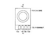
図1〜図3は、本発明の第1の実施の形態の構成を説明するための図である。図1は、実装後の静電駆動型デバイスを真上から見た上面図であり、図2は、図1のA−A部の断面図であり、図3(a)は、突起電極形成後のMEMS基板4を図2の下面方向から見た図であり、図3(b)は、突起電極形成後の回路基板6を図2の上面方向から見た図である。
【0021】
第1の実施の形態は、次のように構成されている。MEMS基板4は、中央部をエッチングで除いた単結晶シリコンの枠7と、この枠7の下面全面に形成されたポリイミド薄膜8及びCr薄膜9と、ポリイミド薄膜8上に円形に形成されたAl反射膜10と、Cr薄膜9上の枠直下の3箇所に形成されたAuの電極パッド11a、11b、11cとからなり、稼動部14は、静電引力により回路基板6方向に湾曲する。
【0022】
一方、回路基板6は、基材60と、Al反射膜10と対向する位置に形成されたAlの駆動電極5と、電極パッド11a、11b、11cの対向する位置に形成されたAlの接続パッド12a、12b、12cと、駆動電極5及び接続パッド12a〜12cと配線によって電気的に接続された外部接続端子13a、13b、13c、13dとからなり、上記した各素子は全て基材60の上面に設けられている。
【0023】
MEMS基板4上の電極パッド11a〜11cには、突起電極としてのAuバンプ15a〜15cが、回路基板6上の接続パッド12a〜12c上には、突起電極としてのAuバンプ16a〜16cがスタッドバンプ法により設けられている。Auバンプ15a〜15c及びAuバンプ16a〜16cは、全て同一形状の円錐であり、大きさは底面径が60〜100μm、頂面径が20〜50μmである。本実施の形態では、Auバンプ15a〜15cは各電極パッド11a〜11c及び接続パッド12a〜12c上に各1個設けたが、可能であれば2つ以上設けてもよく、また、形状も全て同一でなくてもよい。
【0024】
金属電極としてのSn−Biはんだ17a〜17cは、Auバンプ15a〜15cとAuバンプ16a〜16cとを一体的に覆い、各Auバンプ周面と固相拡散接続によって合金層を形成、機械的・電気的に接続している。Sn−Biはんだ17a〜17cの材質はSn42%、Bi58%の低融点はんだとし、Auバンプ15a〜15c及びAuバンプ16a〜16cよりも体積弾性率が低く、塑性変形がしやすいものとする。
【0025】
上記した突起電極と金属電極の組合せは、金属電極の材質が突起電極の材質よりも塑性変形しやすいものであれば、Sn−Biはんだでなくても良く、突起電極がAuバンプの場合は、Sn−ZnやSn−In等の他のはんだ合金やAl、Snを金属電極として使用しても良い。また、突起電極の材質はAuに限らず、NiやCu等体積弾性率が大きいものであれば構わない。
【0026】
(作用)
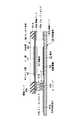
次に、本実施の形態の製造方法について図4〜図9を参照して説明する。図において(S1)〜(S6)は各製造工程を示すものとする。
【0027】
(S1) 先ず図4に示すように、MEMS基板4の電極パッド11a〜11c上に、スタッドバンプ法によりAuバンプ15a〜15cを形成する。回路基板6の接続パッド12a〜12c上にも同様にスタッドバンプ法によりAuバンプ16a〜16cを形成する。Auバンプ15a〜15cを形成する工程とAuバンプ16a〜16cを形成する工程は、どちらを先にしても良い。また、本実施の形態ではAuワイヤを材料としたスタッドバンプ法でAuバンプを形成しているが、メッキ法で形成しても構わない。
【0028】
(S2) 次に図5に示すように、Sn−Biはんだ17a〜17cを、逆円錐形状に穴19a〜19cを設けたNi/Co製のボール整列治具18を用いて、MEMS基板4の電極パッド位置に対応する位置に整列させる。ボール整列治具18は、ネジ止め(図示せず)により基台(図示せず)に固定されている。
【0029】
Auバンプ15a〜15c及び16a〜16cの底面径より大きい球形のSn−Biはんだ17a〜17cを、ボール整列治具18の上面に3個以上載置した後、穴19a〜19cの全てにSn−Biはんだ17a〜17cが挿入されるように金属スキージ20をボール整列治具18上面と水平方向に移動させる。
【0030】
この時、一度、穴19a〜19cに挿入されたSn−Biはんだ17a〜17cに金属スキージ20が接触して損傷しないために、金属スキージ20の下端とボール整列治具18上面との距離hは、
Sn−Biはんだ17a〜17cの直径>h>穴19a〜19cに挿入されたSn−Biはんだ17a〜17cがボール整列治具18上面から露出する高さの関係を満たすように調整される。また、Sn−Biはんだ17a〜17cは、サイズが直径35〜400μmの微小ボールであるので、金属スキージ20の材質をAl等の金属製にし、Sn−Biはんだ17a〜17cが整列中に金属スキージ20に静電付着することを防止する。
【0031】
(S3) 次に、Auバンプ15a〜15cを設けたMEMS基板4と、Sn−Biはんだ17a〜17cの水平方向の位置合わせをする。すなわち、MEMES基板4の背面を、実装機の圧着ヘッド21で真空吸着により保持し、Auバンプ15a〜15cとSn−Biはんだ17a〜17cとが対向するように位置調整する。
【0032】
次に図6に示すように、圧着ヘッド21を垂直に降下させて、Auバンプ15a〜15cをSn−Biはんだ17a〜17cに圧入する動作を開始する。このとき圧着ヘッド21の側面に設けられた垂直方向の測長センサ22によりボール整列治具18の上面と圧着ヘッド21との距離を検出するようにする。ここでの検出には光線100が使用される。これによって、Auバンプ15a〜15cをSn−Biはんだ17a〜17cに圧入する量を制御することができる。
【0033】
Auバンプ15a〜15cをSn−Biはんだ17a〜17cに圧入する前に、予めAuバンプ15a〜15cとSn−Biはんだ17a〜17cの少なくともいずれか一方を固相拡散接続が可能な温度に加熱しておく。加熱方法は、セラミックヒーター(図示せず)を圧着ヘッド21上部または基台(図示せず)内部に設置し、MEMS基板4または回路基板6を介して間接的に加熱する。
【0034】
このときの予熱温度は、Sn−Biはんだ17a〜17cを使用する場合、融点139℃を考慮して100〜138℃が良い。また、圧入する時の圧力は1電極あたり、20〜100gfとする。また、必要に応じて穴19a〜19cを下面側から真空吸着し、圧入中にSn−Biはんだ17a〜17c及びボール整列治具18自身が動かないようにする。
【0035】
(S4) 圧入は次のように進行する。Auバンプ15a〜15cの頂部がSn−Biはんだ17a〜17cの表面に接触する。Sn−Biはんだ17a〜17cの接触部分から突起電極(Auバンプ15a〜15c)頂部の形状にならって塑性変形する。塑性変形時に酸化皮膜が破壊され、Sn−Biはんだ17a〜17cの新生面とAuバンプ15a〜15cの新生面が接触・固相拡散して機械的・電気的に接続する(図7)。
【0036】
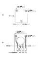
(S5) 圧入完了後に、穴19a〜19cに対する下面からの真空吸着を解除し、MEMS基板4を圧着ヘッド21と共に垂直方向に持ち上げ、Sn−Biはんだ17a〜17cをボール整列治具18から切り離す。次に、回路基板6上のAuバンプ16a〜16cと、MEMS基板4上のSn−Biはんだ17a〜17cとが対向するように圧着ヘッド21を水平方向に移動する。
【0037】
次に、図8に示すように、圧着ヘッド21を垂直に降下させて、Auバンプ16a〜16cをSn−Biはんだ17a〜17cに圧入する動作を開始する。このとき、測長センサ22により、回路基板6の上面と圧着ヘッド21との距離を検出することによりAuバンプ16a〜16cをSn−Biはんだ17a〜17cに圧入する量を制御するようにする。
【0038】
Sn−Biはんだ17a〜17cをAuバンプ16a〜16cに圧入する前に、予めAuバンプ16a〜16cとSn−Biはんだ17a〜17cの少なくともいずれか一方を固相拡散接続が可能な温度に加熱しておく。加熱方法は、セラミックヒーター(図示せず)を圧着ヘッド21上部または基台(図示せず)内部に設置し、MEMS基板4または回路基板6を介して間接的に加熱する。
【0039】
このときの予熱温度は、Sn−Biはんだ17a〜17cを使用する場合、融点139℃を考慮して100〜138℃、圧入する時の圧力は1電極あたり、20〜100gfとする。
【0040】
(S6) 圧入は、次のように進行する。Auバンプ16a〜16cの頂部がSn−Biはんだ17a〜17cの表面に接触する。Sn−Biはんだ17a〜17cの接触部分からAuバンプ16a〜16c頂部の形状にならって塑性変形する。塑性変形時に酸化皮膜が破壊され、Sn−Biはんだ17a〜17cの新生面とAuバンプ16a〜16cの新生面が接触・固相拡散して機械的・電気的に接続する(図9)。
【0041】
上記した第1の実施の形態に係る製造方法では、MEMS基板4のAuバンプ15a〜15cとSn−Biはんだ17a〜17cとを先に固相拡散接続し、後工程で回路基板6のAuバンプ16a〜16cとSn−Biはんだ17a〜17cを固相拡散接続したが、逆の工程にしても差し支えない。また、第1の実施の形態では大気中で製造を行っているが、真空中またはArガス等の不活性ガス中で実施しても良い。
【0042】
(効果)
MEMS基板4の電極パッド11a〜11cと、回路基板6の接続パッド12a〜12bとの間を電気的・機械的に支持するバンプ部は、Sn−Biはんだ17a〜17cとAuバンプ15a〜15c及びAuバンプ16a〜16cの周面全体とで固相拡散接続をしているので、バンプ接続部の機械強度が向上するという効果がある。
【0043】
また、第1の実施の形態には、上記の効果のほかに、次のような特有の効果がある。すなわち、Auバンプ15a〜15cと、Auバンプ16a〜16cとが直接接触しないので、MEMS基板4と回路基板6間のギャップ量を自由に大きくとることが可能であり、その結果、高ギャップ量のフリップチップ接続が可能となる。
【0044】
[第2の実施の形態]
本発明の第2の実施の形態は、受光素子を有する光半導体チップとガラス基板とを、フリップチップ接続する半導体装置に適用したものである。
【0045】
(構成)
図10は、本発明の第2の実施の形態の構成を説明するための図である。第2の実施の形態は、次のように構成されている。光半導体チップ24は、シリコン基材25と、このシリコン基材25の下面の中央部に設けられた受光素子23と、この受光素子23と配線を介して電気的に接続されたAlの電極パッド26とからなる。
【0046】
一方、ガラス基板27は、ガラス基材28とAlの接続パッド29と外部端子(図示せず)とからなる。接続パッド29は、光半導体チップ24の電極パッド26に対向する位置に配置される。外部接続端子は、接続パッド29と配線を介して電気的に接続される。
【0047】
光半導体チップ24の電極パッド26の一面及びガラス基板27の接続パッド29の一面には、スタッドバンプ法によりそれぞれAuバンプ30、Auバンプ31が設けられている。Auバンプ30,31は、底部径が60〜100μm、頂部径が20〜50μm、高さが15〜60μmの円錐形状をしている。Auバンプ30とAuバンプ31は、互いが対向しない位置に配置され、Al合金32とAuバンプ30,31の周面全体で固相拡散接続されている。
【0048】
次に、第2の実施の形態の製造方法について図11〜図15を用いて説明する。図において(S101)〜(S105)は各製造工程を示すものとする。
【0049】
(S101) まず図11に示すように、光半導体チップ24の電極パッド26上にAuバンプ30を形成する。また、ガラス基板27の接続パッド29上にAuバンプ31を形成する。
【0050】
(S102) 次に図12に示すように、直径100〜200μmのAlボール35を、Al製の金属スキージ36を水平方向に移動してボール整列治具33の穴34a中に整列・配置する。
【0051】
(S103) 次に、ボール整列治具33の穴34bの下面から真空吸着してAlボール35を固定した後、レベリングプレート52を用いて押圧し、Alボール35を円筒状のAl合金32に成型する(図13)。
【0052】
(S104) Auバンプ31を接続パッド29上に形成したガラス基板27を圧着ヘッド37に吸着保持した後、ボール整列治具33上のAl合金32と、ガラス基板27の接続パッド29とが対向するように水平移動する。
【0053】
次に図14に示すように、圧着ヘッド37を垂直に降下させてAuバンプ31とAl合金32とを接触させた後、垂直方向に圧力を加えつつ、水平方向に超音波振動200を付与する。これによりAuバンプ31はAl合金32に圧入し、塑性変形した金属電極としてのAl合金32の新生面とAuバンプ31の新生面が接触することで固相拡散接続が完了する。また、Auバンプ31を形成した以外の接続パッド29とAl合金32の周面も同時に固相拡散接続が完了する。
【0054】
(S105) 次に、Auバンプ31とAl合金32が固相拡散接続されたガラス基板27を基台(図示せず)上に固定した後、Auバンプ30を電極パッド26上に形成した光半導体チップ24を圧着ヘッド37に吸着保持する。
【0055】
次に、圧着ヘッド37を垂直に降下させ、Auバンプ30とAl合金32とを接触させた後、垂直方向に圧力を加えつつ、水平方向に超音波振動200を付与する。これによりAuバンプ30はAl合金32に圧入し、塑性変形したAl合金32の新生面とAuバンプ30の新生面が接触することで固相拡散接続が完了する。また、Auバンプ30を形成した以外の接続パッド26とAl合金32の周面も同時に固相拡散接続が完了する(図15)。
【0056】
(効果)
光半導体チップ24の電極パッド26と、ガラス基板27の接続パッド29との間を電気的・機械的に支持するバンプ部は、第1にAl合金32とAuバンプ30及びAuバンプ31の周面全体が固相拡散接続され、第2にAl合金32の周面と電極パッド26とが固相拡散され、第3にAl合金32の周面と接続パッド29とがそれぞれで固相拡散接続されるので、バンプ部の機械的強度が向上するという効果がある。
【0057】
第2の実施の形態には、上記の効果のほかに次のような特有の効果がある。すなわち、Auバンプ30とAuバンプ31が対向していないので、光半導体チップ24とガラス基板27間のギャップ量を小さくすることが可能となる。また、Al合金32とAuバンプ30、31の周面以外でも固相拡散接続しているので、最も接続強度が向上できる。さらに、温度をかけずに実装できるので熱に弱い部品も実装可能となる。さらに、電極パッドの面積を大きくとることができる。
【0058】
[第3の実施の形態]
本発明の第3の実施の形態は、基板の大部分に稼動部を有するMEMS基板と稼動部に対応する駆動電極を有する回路基板とをフリップチップ接続して静電駆動型デバイスを実装した例に適用したものである。
【0059】
(構成)
図16及び図17(a)、(b)は、本発明の第3の実施の形態の構成を説明するための図である。第3の実施の形態は次のように構成されている。MEMS基板44は、中央部をエッチングで除いた単結晶シリコンの枠45と、この単結晶シリコンの枠45の下面全面に形成されたポリイミド薄膜46及びCr薄膜47と、ポリイミド薄膜46上に円形に形成されたAl反射膜48と、Cr薄膜47上の枠直下の3箇所に形成されたAuの電極パッド49a、49b、49cとからなり、稼動部50は、静電引力により回路基板38方向に湾曲する。
【0060】
一方、回路基板38は、基材70と、Al反射膜48と対向する位置に形成されたAlの駆動電極39と、電極パッド49a、49b、49cの対向する位置に形成されたAlの接続パッド40a、40b、40cと、駆動電極39及び接続パッド40a〜40cと配線によって電気的に接続された外部接続端子41a〜41dとからなり、上記した各素子は全て基材70の上面に設けられている。
【0061】
MEMS基板44上の電極パッド49a〜49cには、Auバンプ51a〜51cが、回路基板38上の接続パッド40a〜40cには、Niバンプ42a〜42cがメッキ法により均一な高さになるように設けられている。Auバンプ51a〜51cは、全て同一形状の円錐であり、大きさは底面径が60〜100μm、頂面径が20〜50μm、高さが15〜60μmである。
【0062】
Auバンプ51a〜51cの高さはレベリング治具(図示せず)によって15〜60μmの間で均一化されている。Niバンプ42a〜42cは、全て同一の円筒形状であり、Auバンプ51a〜51cの頂面径以上の直径である。
【0063】
Sn−Znはんだ43a〜43cは、Auバンプ51a〜51cとNiバンプ42a〜42cを一体的に覆い、各バンプ51a〜51c、42a〜42c周面と固相拡散接続によって合金層を形成して機械的・電気的に接続している。Sn−Znはんだ43a〜43cの組成はSn91%、Zn9%とし、Auバンプ51a〜51c及びNiバンプ42a〜42cよりも体積弾性率が低く、塑性変形がしやすいものとする。
【0064】
(作用・効果)
次に、この発明の実施の形態の作用を説明する。MEMS基板44の電極パッド49a〜49cと、回路基板38の接続パッド40a〜40bとの間を電気的・機械的に支持するバンプ部について、Auバンプ51a〜51cとNiバンプ42a〜42cの頂面同士が接触し、基板間のギャップ量をAuバンプ高さとNiバンプ高さの和に維持する。Sn−Znはんだ43a〜43cは、Auバンプ51a〜51c及びNiバンプ42a〜42cの側面全体で固相拡散接続をしており、バンプ部の機械的強度が向上するという効果がある。
【0065】
また、第3の実施の形態には、上記の効果のほかに、次のような特有の効果がある。すなわち、高さが均一なAuバンプ51a〜51cとNiバンプ42a〜42cとで、基板間のギャップ量を維持できる。その結果、圧着ヘッドの垂直方向への位置制御の分解能とは無関係に素子を実装可能となり、高価な設備を使用しなくてもよい。
【0066】
(付記)
上記した具体的な実施の形態から以下のような構成の発明が抽出可能である。
【0067】
1. 電極パッドを有する半導体チップを、前記電極パッドに対向する位置に接続パッドを有する回路基板に、バンプを介して実装する半導体装置において、
前記バンプは、
前記電極パッドに設けた第1の突起電極と、
前記接続パッドに設けた第2の突起電極と、
前記第1及び第2の突起電極の周面を一体的に被覆し、且つこれら2つの突起電極を固相拡散により接続する導電性の接続部材と、
を具備することを特徴とする半導体装置。
【0068】
2. 前記接続部材の体積弾性率は、前記第1及び第2の突起電極の体積弾性率よりも小さいことを特徴とする1.に記載の半導体装置。
【0069】
(対応する発明の実施の形態)
この発明に関する実施の形態は、少なくとも第1〜第3の実施の形態が対応する。構成中の第1の突起電極は、第1の実施形態ではAuバンプ15a〜15c、第2の実施の形態ではAuバンプ30、第3の実施の形態ではAuバンプ51a〜51cが該当する。構成中の第2の突起電極は、第1の実施の形態ではAuバンプ16a〜16c、第2の実施の形態ではAuバンプ31、第3の実施の形態ではNiバンプ42a〜42cが該当する。構成中の導電性の接続部材は、第1の実施の形態ではSn−Biはんだ17a〜17c、第2の実施の形態ではAl合金32、第3の実施の形態ではSn−Znはんだ43a〜43cが該当する。
【0070】
(作用・効果)
導電性の接続部材と、第1の突起電極及び第2の突起電極、両方の周面全体で固相拡散接続しているので接続面積が大きく取れ、且つアンカー効果によりバンプ接続部の機械強度が向上できる。また、導電性の接続部材を第1の突起電極及び第2の突起電極よりも体積弾性率の小さい材質としているために、従来と比較して導電性の接続部材が低圧力で優先的に塑性変形して第1の突起電極及び第2の突起電極と固相拡散接続する。その結果、接続時に半導体チップの電極パッド及び回路基板の接続パッドに加わる圧力が低減し、ヒンジや薄膜といった脆弱なMEMS基板や極薄の半導体チップ及び回路基板を破壊せずに実装することができる。また、第1の突起電極と第2の突起電極は接触しないので、実装設備によって基板間のキャップ量を自由に調整できる。
【0071】
3. 前記接続部材は、前記2つの突起電極を、前記電極パッド及び前記接続パッドと併せて固相拡散接続することを特徴とする1.に記載の半導体装置。
【0072】
(対応する発明の実施の形態)
この発明に関する実施の形態は、少なくとも第2の実施の形態が対応する。構成中の第1の突起電極はAuバンプ30、第2の突起電極はAuバンプ31、導電性の接続部材はAl合金32、電極パッドはAlの電極パッド26、接続パッドはAlの接続パッド29が該当する。
【0073】
(作用・効果)
導電性の接続部材は、第1の突起電極及び第2の突起電極、両方の周面全体に加えて電極パッドと接続パッドとも固相拡散接続をしている。その結果、バンプ接続部と電極パッド及び接続パッド界面部との機械的強度が向上する。
【0074】
4. 前記第1の突起電極と前記第2の突起電極とが対向しないことを特徴とする1.に記載の半導体装置。
【0075】
(対応する発明の実施の形態)
この発明に関する実施の形態は、少なくとも第2の実施の形態が対応する。構成中の第1の突起電極はAuバンプ30、第2の突起電極はAuバンプ31が該当する。
【0076】
(作用・効果)
第1の突起電極と第2の突起電極の周面は対向しないので、互いに接触せず且つ上下方向にも重ならない位置で導電性の接続部材と固相拡散接続でき、半導体チップと回路基板間のギャップ量を小さくできる。ギャップ量が小さくできると、静電駆動型MEMSデバイスの低電圧駆動が実現できる。
【0077】
5. 前記第1の突起電極と、前記第2の突起電極の頂部が対向し、且つ接触していることを特徴とする1.に記載の半導体装置。
【0078】
(対応する発明の実施の形態)
この発明に関する実施の形態は、少なくとも第3の実施の形態が対応する。構成中の第1の突起電極はAuバンプ51a〜51c、第2の突起電極はNiバンプ42a〜42cが該当する。
【0079】
(作用・効果)
第1の突起電極の頂部と第2の突起電極の頂部とが接触(ここでは面接触)した状態で、導電性の接続部材と第1及び第2の突起電極周面が固相拡散接続している。その結果、突起電極の高さに基づいて基板間のギャップ量の制御が可能となり、高精度な実装設備(センサー及び関連する制御系など)を使わずに高精度なギャップ量が要求される光半導体チップを安定して実装できる。
【0080】
6. 前記接続部材の、前記第1及び第2の突起電極が接続される接続面は平坦形状であることを特徴とする1.に記載の半導体装置。
【0081】
(対応する発明の実施の形態)
この発明に関する実施の形態は、少なくとも第2の実施の形態が対応する。接続部材の接続面は、ボール整列治具33に配置したAlボール35をレベリングプレート36で押圧し円筒状に成型することにより平坦形状とされる。
【0082】
(作用・効果)
圧着工程において、Al合金の圧入面が平坦なため、Auバンプ30及び31の頂面が垂直にAl合金へ圧入できる。その結果、圧入不良を防止でき、光半導体チップ等の実装を安定して行えるという効果がある。
【0083】
7. 半導体チップの電極パッド面上に第1の突起電極を形成する工程と、
回路基板の接続パッド上に第2の突起電極を形成する工程と、
前記電極パッド又は前記接続パッドと対向する位置に導電性の接続部材を整列・配置する工程と、
前記接続部材と前記第1の突起電極とを位置合わせした後に、前記第1及び前記第2の突起電極の周面を一体的に被覆するように固相拡散接続する工程と、
前記接続部材と前記第2の突起電極とを位置合わせした後に、前記第1及び前記第2の突起電極の周面を一体的に被覆するように固相拡散接続する工程と、
を具備することを特徴とする半導体装置の製造方法。
【0084】
(対応する発明の実施の形態)
この発明に関する実施の形態は、少なくとも第1の実施の形態が対応する。第1の突起電極を形成する工程は、第1の実施の形態ではMEMS基板4上の電極パッド11a〜11cにAuバンプ15a〜15cを形成する工程、第3の実施の形態ではMEMS基板44上の電極パッド49a〜49cにAuバンプ51a〜51cを形成する工程が該当する。
【0085】
第2の突起電極を形成する工程は、第1の実施の形態では回路基板6上の接続パッド12a〜12cにAuバンプ16a〜16cを形成する工程が該当する。
【0086】
接続部材を前記電極パッド又は接続パッドと対向する位置に整列・配置する工程は、第1の実施の形態ではSn−Biはんだをボール整列治具18を用いて整列・配置する工程が該当する。
【0087】
前記接続部材と前記第1の突起電極とを位置合わせした後に固相拡散接続する工程は、第1の実施の形態では、測長センサ22付の圧着ヘッド21でMEMS基板4を保持してSn−Biはんだ17a〜17cとAuバンプ15a〜15cとの水平方向の位置合わせを行ない、加熱・加圧して固相拡散接続する工程が該当する。
【0088】
前記接続部材と前記第2の突起電極とを位置合わせした後に固相拡散接続する工程は、第1の実施の形態では測長センサ22付の圧着ヘッド21で回路基板6を保持してSn−Biはんだ17a〜17cとAuバンプ16a〜16cとの水平方向の位置合わせを行ない、加熱・加圧して固相拡散接続する工程が該当する。
【0089】
(作用・効果)
1.に記載した構成の作用・効果と同じである。
【0090】
8. 前記接続部材を前記電極パッド又は前記接続パッドと対向する位置に整列・配置する工程の後に、前記接続部材の接続面を平坦化する工程をさらに具備することを特徴とする7.に記載の半導体装置の製造方法。
【0091】
(対応する発明の実施の形態)
この発明に関する実施の形態は、少なくとも第2の実施の形態が対応する。接続部材を平坦化する工程は、第2の実施の形態ではボール整列治具33に配置したAlボール35をレベリングプレート52で押圧し、円筒状に成型する工程が該当する。
【0092】
(作用・効果)
圧着工程において、Al合金の圧入面が平坦なため、Auバンプ30及び31の頂面が垂直にAl合金へ圧入できる。その結果、圧入不良を防止でき、光半導体チップ等の実装を安定して行なえるという効果がある。
【0093】
9. 前記導電性の接続部材は、球形であることを特徴とする7.に記載の半導体装置の製造方法。
【0094】
(対応する発明の実施の形態)
この発明に関する実施の形態は、第1〜3の実施の形態が対応する。接続部材は、第1の実施の形態ではSn−Biはんだ17a〜17c、第2の実施の形態ではAlボール35、第3の実施の形態ではSn−Znはんだ43a〜43cが該当する。
【0095】
(作用・効果)
接続部材が球形のため、金属スキージで水平方向に移動させやすい。その結果、ボール整列治具の穴に容易に配置しやすくなり、その結果、光半導体チップ等の量産化が容易となる。
【0096】
【発明の効果】
本発明によれば、第1及び第2の突起電極、両方の周面全体で導電性の接続部材と固相拡散接続したので接続面積を大幅に増加することが可能となり、これによって、突起電極同士の機械的強度を向上させることができる。
【0097】
また、本発明によれば、樹脂封止がむずかしい光半導体チップや機械駆動部を有するMEMS基板の実装にも適用可能となり、さらには、ヒンジや薄膜といった脆弱なMEMS基板や極薄の半導体チップ及び回路基板を破壊せずに実装することができるという効果がある。
【図面の簡単な説明】
【図1】本発明の第1の実施の形態の構成を説明するための図であり、実装後の静電駆動型デバイスを真上から見た上面図である。
【図2】本発明の第1の実施の形態の構成を説明するための図であり、図1のA−A部の断面図である。
【図3】本発明の第1の実施の形態の構成を説明するための図であり、(a)は突起電極形成後のMEMS基板4を図2の下面方向から見た図であり、(b)は、突起電極形成後の回路基板6を図2の上面方向から見た図である。
【図4】本発明の第1の実施の形態の製造方法について説明するための図(その1)である。
【図5】本発明の第1の実施の形態の製造方法について説明するための図(その2)である。
【図6】本発明の第1の実施の形態の製造方法について説明するための図(その3)である。
【図7】本発明の第1の実施の形態の製造方法について説明するための図(その4)である。
【図8】本発明の第1の実施の形態の製造方法について説明するための図(その5)である。
【図9】本発明の第1の実施の形態の製造方法について説明するための図(その6)である。
【図10】本発明の第2の実施の形態の構成を説明するための図である。
【図11】本発明の第2の実施の形態の製造方法について説明するための図(その1)である。
【図12】本発明の第2の実施の形態の製造方法について説明するための図(その2)である。
【図13】本発明の第2の実施の形態の製造方法について説明するための図(その3)である。
【図14】本発明の第2の実施の形態の製造方法について説明するための図(その4)である。
【図15】本発明の第2の実施の形態の製造方法について説明するための図(その5)である。
【図16】本発明の第3の実施の形態の構成を説明するための図(その1)である。
【図17】本発明の第3の実施の形態の構成を説明するための図(その2)である。
【図18】従来の半導体装置の構成について説明するための図である。
【符号の説明】
4…MEMS基板、5…駆動電極、6…回路基板、7…枠、8…ポリイミド膜、9…Cr膜、10…Al反射膜、11a〜11c…電極パッド、12a〜12c…接続パッド、13a〜13d…外部接続端子、14…稼動部、15a〜15c…Auバンプ、16a〜16c…Auバンプ、17a〜17c…Sn−Biはんだ、60…基材。[0001]
BACKGROUND OF THE INVENTION
The present invention relates to a semiconductor device.Made of tableIt relates to the manufacturing method.
[0002]
[Prior art]
In order to reduce the size of electronic equipment, it is important to develop a high-density mounting technique that improves the mounting density of semiconductor devices. As a high-density mounting technique considered to be most effective, there is a flip chip mounting method in which a semiconductor chip and an electrode of a circuit board are connected by a bump.
[0003]
In the flip chip mounting method, since the connection is completed within the main surface of the semiconductor chip to be mounted and the circuit board, the mounting area can be reduced to a size substantially equal to that of the semiconductor chip.
[0004]
Japanese Patent No. 3297254 discloses a semiconductor package using such flip chip mounting and a manufacturing method thereof. As shown in FIG. 18, the semiconductor package disclosed in the publication has a substrate 2 provided on one main surface with a wiring portion in which a protruding electrode 2b is provided on the surface of a conductor terminal 2a, and a protruding electrode 2b of the substrate 2. The semiconductor chip 1 connected and mounted in a face-down manner in correspondence with the protruding electrode 1b provided on the
[0005]
The semiconductor package disclosed in the publication includes a step of forming a protruding electrode 2b on the surface of the conductor terminal 2a of the substrate 2, a step of forming the protruding electrode 1b on the surface of the
[0006]
[Problems to be solved by the invention]
However, in the solid phase diffusion connection of the semiconductor package described above, since the protruding electrode 1b of the semiconductor chip 1 and the protruding electrode 2b of the substrate 2 are connected only at the top of each, the connection area is small, and the solder connection The mechanical strength is weaker than the connection by liquid phase diffusion in which the protruding electrode is once melted.
[0007]
Therefore, a process of mechanically reinforcing the gap between the lower surface of the semiconductor chip 1 and the upper surface of the substrate 2 with a sealing resin is essential. As a result, there has been a problem that it is difficult to apply to flip chip mounting of semiconductor chips that are difficult to encapsulate, such as optical semiconductor chips such as surface emitting lasers and PDs, and MEMS substrates having mechanical drive units.
[0008]
The present invention has been made by paying attention to such a problem, and the object is to improve the mechanical strength by increasing the connection area between the protruding electrode of the semiconductor chip and the protruding electrode of the substrate. DressSetIt is to provide a manufacturing method.
[0009]
[Means for Solving the Problems]
To achieve the above objective,In the method for manufacturing a semiconductor device according to the first aspect of the present invention, the step of forming the first protruding electrode on the electrode pad surface of the semiconductor chip and the formation of the second protruding electrode on the connection pad of the circuit board are performed. A step of aligning and arranging a conductive connection member at a position facing the electrode pad or the connection pad, and aligning the connection member and the first protruding electrode; After solid phase diffusion connection so as to integrally cover the peripheral surface of the electrode, and aligning the connecting member and the second protruding electrode, the peripheral surface of the second protruding electrode is integrated Solid phase diffusion connection so as to cover.
[0010]
Also,A method for manufacturing a semiconductor device according to a second aspect of the present invention further includes a step of planarizing a connection surface of the connection member in the method for manufacturing a semiconductor device according to the first aspect.
[0011]
Also,A method for manufacturing a semiconductor device according to a third aspect of the present invention is the method for manufacturing a semiconductor device according to the first aspect, wherein the conductive connecting member is spherical.
[0018]
DETAILED DESCRIPTION OF THE INVENTION
Hereinafter, embodiments of the present invention will be described in detail with reference to the accompanying drawings.
[0019]
[First embodiment]
In the first embodiment, an electrostatic drive type device is mounted by flip-chip connecting a MEMS substrate as a semiconductor chip having a working part on the majority of the substrate and a circuit board having a drive electrode corresponding to the working part. Applied to the example.
[0020]
(Constitution)
1-3 is a figure for demonstrating the structure of the 1st Embodiment of this invention. 1 is a top view of the electrostatic drive device after mounting as viewed from directly above, FIG. 2 is a cross-sectional view taken along line AA of FIG. 1, and FIG. FIG. 3B is a view of the subsequent MEMS substrate 4 as viewed from the lower surface direction of FIG. 2, and FIG.
[0021]
The first embodiment is configured as follows. The MEMS substrate 4 includes a single-
[0022]
On the other hand, the circuit board 6 includes a
[0023]
[0024]
The Sn-Bi solders 17a to 17c as metal electrodes integrally cover the
[0025]
The combination of the protruding electrode and the metal electrode described above may not be Sn-Bi solder as long as the material of the metal electrode is more easily plastically deformed than the material of the protruding electrode. If the protruding electrode is an Au bump, Other solder alloys such as Sn—Zn and Sn—In, Al, and Sn may be used as the metal electrode. Further, the material of the protruding electrode is not limited to Au, and any material having a large volume modulus such as Ni or Cu may be used.
[0026]
(Function)
Next, the manufacturing method of this Embodiment is demonstrated with reference to FIGS. In the figure, (S1) to (S6) indicate manufacturing steps.
[0027]
(S1) First, as shown in FIG. 4, Au bumps 15a to 15c are formed on the electrode pads 11a to 11c of the MEMS substrate 4 by a stud bump method. Similarly, Au bumps 16a to 16c are formed on the
[0028]
(S2) Next, as shown in FIG. 5, the Sn-Bi solders 17a to 17c are bonded to the MEMS substrate 4 using a Ni / Co
[0029]
After three or more spherical Sn-Bi solders 17a to 17c larger than the bottom diameters of the Au bumps 15a to 15c and 16a to 16c are placed on the upper surface of the
[0030]
At this time, the distance h between the lower end of the
The diameter of the Sn-Bi solders 17a to 17c> h> the Sn-Bi solders 17a to 17c inserted into the
[0031]
(S3) Next, the horizontal alignment of the MEMS substrate 4 provided with the Au bumps 15a to 15c and the Sn-Bi solders 17a to 17c is performed. That is, the back surface of the MEMES substrate 4 is held by vacuum suction with the crimping
[0032]
Next, as shown in FIG. 6, the operation of pressing the Au bumps 15 a to 15 c into the Sn—Bi solders 17 a to 17 c is started by vertically lowering the crimping
[0033]
Before the Au bumps 15a to 15c are press-fitted into the Sn-Bi solders 17a to 17c, at least one of the Au bumps 15a to 15c and the Sn-Bi solders 17a to 17c is heated to a temperature at which solid phase diffusion connection is possible. Keep it. In the heating method, a ceramic heater (not shown) is installed on the upper part of the crimping
[0034]
The preheating temperature at this time is preferably 100 to 138 ° C. in consideration of the melting point of 139 ° C. when the Sn—Bi solders 17 a to 17 c are used. Moreover, the pressure at the time of press-fitting shall be 20-100 gf per electrode. Further, if necessary, the
[0035]
(S4) The press-fitting proceeds as follows. The top portions of the Au bumps 15a to 15c are in contact with the surfaces of the Sn-Bi solders 17a to 17c. The plastic deformation is performed in accordance with the shape of the tops of the protruding electrodes (Au bumps 15a to 15c) from the contact portions of the Sn-Bi solders 17a to 17c. The oxide film is destroyed at the time of plastic deformation, and the new surfaces of the Sn-Bi solders 17a to 17c and the new surfaces of the Au bumps 15a to 15c are contacted / solid phase diffused and mechanically / electrically connected (FIG. 7).
[0036]
(S5) After the press-fitting is completed, the vacuum suction from the lower surface to the
[0037]
Next, as shown in FIG. 8, the operation of pressing the Au bumps 16a to 16c into the Sn-Bi solders 17a to 17c is started by lowering the crimping
[0038]
Before the Sn-Bi solders 17a to 17c are press-fitted into the Au bumps 16a to 16c, at least one of the Au bumps 16a to 16c and the Sn-Bi solders 17a to 17c is heated to a temperature at which solid phase diffusion connection is possible. Keep it. In the heating method, a ceramic heater (not shown) is installed on the upper part of the crimping
[0039]
When using Sn-Bi solders 17a to 17c, the preheating temperature at this time is 100 to 138 ° C. in consideration of the melting point of 139 ° C., and the pressure at the time of press-fitting is 20 to 100 gf per electrode.
[0040]
(S6) The press-fitting proceeds as follows. The tops of the Au bumps 16a to 16c are in contact with the surfaces of the Sn-Bi solders 17a to 17c. The plastic deformation occurs in the shape of the top of the Au bumps 16a to 16c from the contact portion of the Sn-Bi solders 17a to 17c. The oxide film is destroyed at the time of plastic deformation, and the new surface of the Sn-Bi solders 17a to 17c and the new surface of the Au bumps 16a to 16c are contacted / solid phase diffused and mechanically / electrically connected (FIG. 9).
[0041]
In the manufacturing method according to the first embodiment described above, the Au bumps 15a to 15c of the MEMS substrate 4 and the Sn-Bi solders 17a to 17c are first solid phase diffusion-connected, and the Au bumps of the circuit board 6 are processed in a later process. Although 16a to 16c and Sn-Bi solders 17a to 17c are connected by solid phase diffusion, they may be reversed. In the first embodiment, the manufacturing is performed in the atmosphere. However, the manufacturing may be performed in a vacuum or an inert gas such as Ar gas.
[0042]
(effect)
Bump portions that electrically and mechanically support between the electrode pads 11a to 11c of the MEMS substrate 4 and the
[0043]
In addition to the above-described effects, the first embodiment has the following specific effects. That is, since the Au bumps 15a to 15c and the Au bumps 16a to 16c are not in direct contact with each other, the gap amount between the MEMS substrate 4 and the circuit substrate 6 can be freely increased. As a result, a high gap amount can be obtained. Flip chip connection is possible.
[0044]
[Second Embodiment]
The second embodiment of the present invention is applied to a semiconductor device in which an optical semiconductor chip having a light receiving element and a glass substrate are flip-chip connected.
[0045]
(Constitution)
FIG. 10 is a diagram for explaining the configuration of the second exemplary embodiment of the present invention. The second embodiment is configured as follows. The
[0046]
On the other hand, the
[0047]
An
[0048]
Next, the manufacturing method of 2nd Embodiment is demonstrated using FIGS. In the figure, (S101) to (S105) indicate each manufacturing process.
[0049]
(S101) First, as shown in FIG. 11, Au bumps 30 are formed on the
[0050]
(S102) Next, as shown in FIG. 12, the
[0051]
(S103) Next, the
[0052]
(S104) After the
[0053]
Next, as shown in FIG. 14, the crimping
[0054]
(S105) Next, after fixing the
[0055]
Next, the crimping
[0056]
(effect)
Bump portions that electrically and mechanically support between the
[0057]
The second embodiment has the following specific effects in addition to the above effects. That is, since the
[0058]
[Third embodiment]
The third embodiment of the present invention is an example in which an electrostatic drive type device is mounted by flip-chip connecting a MEMS substrate having an operation part to a large part of a substrate and a circuit board having a drive electrode corresponding to the operation part. Is applied.
[0059]
(Constitution)
FIG. 16 and FIGS. 17A and 17B are diagrams for explaining the configuration of the third exemplary embodiment of the present invention. The third embodiment is configured as follows. The MEMS substrate 44 is formed in a circular shape on a single crystal silicon frame 45 obtained by removing the central portion by etching, a polyimide
[0060]
On the other hand, the circuit board 38 includes a base material 70, an
[0061]
Au bumps 51a to 51c are formed on the electrode pads 49a to 49c on the MEMS substrate 44, and Ni bumps 42a to 42c are formed on the connection pads 40a to 40c on the circuit board 38 to have a uniform height by plating. Is provided. Each of the Au bumps 51a to 51c is a cone having the same shape, and has a bottom surface diameter of 60 to 100 μm, a top surface diameter of 20 to 50 μm, and a height of 15 to 60 μm.
[0062]
The height of the Au bumps 51a to 51c is made uniform between 15 and 60 μm by a leveling jig (not shown). The Ni bumps 42a to 42c all have the same cylindrical shape, and have a diameter equal to or larger than the top surface diameter of the Au bumps 51a to 51c.
[0063]
The Sn—Zn solders 43a to 43c integrally cover the Au bumps 51a to 51c and the Ni bumps 42a to 42c, and form an alloy layer by solid phase diffusion connection with the bumps 51a to 51c and 42a to 42c. Connected electrically and electrically. The compositions of the Sn—Zn solders 43a to 43c are Sn 91% and Zn 9%. The volume elastic modulus is lower than that of the Au bumps 51a to 51c and the Ni bumps 42a to 42c, and plastic deformation is likely to occur.
[0064]
(Action / Effect)
Next, the operation of the embodiment of the present invention will be described. Top surfaces of the Au bumps 51a to 51c and the Ni bumps 42a to 42c with respect to bump portions that electrically and mechanically support between the electrode pads 49a to 49c of the MEMS substrate 44 and the connection pads 40a to 40b of the circuit board 38. They are in contact with each other, and the gap amount between the substrates is maintained at the sum of the Au bump height and the Ni bump height. The Sn—Zn solders 43a to 43c are in solid phase diffusion connection over the entire side surfaces of the Au bumps 51a to 51c and the Ni bumps 42a to 42c, and there is an effect that the mechanical strength of the bump portion is improved.
[0065]
In addition to the above effects, the third embodiment has the following specific effects. That is, the gap amount between the substrates can be maintained by the Au bumps 51a to 51c and the Ni bumps 42a to 42c having a uniform height. As a result, the element can be mounted regardless of the resolution of the position control of the crimping head in the vertical direction, and expensive equipment need not be used.
[0066]
(Appendix)
Inventions having the following configurations can be extracted from the specific embodiments described above.
[0067]
1. In a semiconductor device for mounting a semiconductor chip having an electrode pad on a circuit board having a connection pad at a position facing the electrode pad via a bump,
The bump is
A first protruding electrode provided on the electrode pad;
A second protruding electrode provided on the connection pad;
A conductive connecting member that integrally covers the peripheral surfaces of the first and second protruding electrodes and connects the two protruding electrodes by solid phase diffusion;
A semiconductor device comprising:
[0068]
2. The connecting member has a bulk modulus of elasticity smaller than that of the first and second protruding electrodes. A semiconductor device according to 1.
[0069]
(Corresponding Embodiment of the Invention)
At least the first to third embodiments correspond to the embodiments relating to the present invention. The first protruding electrodes in the configuration correspond to Au bumps 15a to 15c in the first embodiment, Au bumps 30 in the second embodiment, and Au bumps 51a to 51c in the third embodiment. The second protruding electrodes in the configuration correspond to Au bumps 16a to 16c in the first embodiment, Au bumps 31 in the second embodiment, and Ni bumps 42a to 42c in the third embodiment. The conductive connecting members in the structure are Sn-Bi solders 17a to 17c in the first embodiment,
[0070]
(Action / Effect)
Since the conductive connection member and the first protrusion electrode and the second protrusion electrode are both solid-phase diffusion connected over the entire peripheral surface, the connection area can be increased, and the mechanical strength of the bump connection portion can be increased by the anchor effect. It can be improved. In addition, since the conductive connecting member is made of a material having a smaller volume modulus of elasticity than the first protruding electrode and the second protruding electrode, the conductive connecting member is preferentially plastic at a lower pressure than in the past. Deformation and solid phase diffusion connection are established with the first and second protruding electrodes. As a result, the pressure applied to the electrode pads of the semiconductor chip and the connection pads of the circuit board at the time of connection is reduced, and it is possible to mount a fragile MEMS substrate such as a hinge or a thin film or an ultrathin semiconductor chip and circuit board without destroying them. . In addition, since the first protruding electrode and the second protruding electrode are not in contact with each other, the amount of cap between the substrates can be freely adjusted by the mounting equipment.
[0071]
3. The connection member connects the two protruding electrodes together with the electrode pad and the connection pad by solid phase diffusion connection. A semiconductor device according to 1.
[0072]
(Corresponding Embodiment of the Invention)
The embodiment relating to the present invention corresponds to at least the second embodiment. The first bump electrode in the configuration is
[0073]
(Action / Effect)
The conductive connection member is in solid phase diffusion connection with the electrode pad and the connection pad in addition to the entire surface of the first and second protrusion electrodes and both. As a result, the mechanical strength between the bump connection portion, the electrode pad, and the connection pad interface portion is improved.
[0074]
4). 1. The first protruding electrode and the second protruding electrode do not face each other. A semiconductor device according to 1.
[0075]
(Corresponding Embodiment of the Invention)
The embodiment relating to the present invention corresponds to at least the second embodiment. The first bump electrode in the structure corresponds to the
[0076]
(Action / Effect)
Since the peripheral surfaces of the first protruding electrode and the second protruding electrode do not face each other, the conductive connection member and the solid phase diffusion connection can be made at a position where they do not contact each other and do not overlap in the vertical direction. The gap amount can be reduced. When the gap amount can be reduced, low voltage driving of the electrostatic drive type MEMS device can be realized.
[0077]
5. 1. The top of the first protruding electrode and the second protruding electrode are opposed to and in contact with each other. A semiconductor device according to 1.
[0078]
(Corresponding Embodiment of the Invention)
The embodiment relating to the present invention corresponds to at least the third embodiment. The first protruding electrodes in the configuration correspond to Au bumps 51a to 51c, and the second protruding electrodes correspond to Ni bumps 42a to 42c.
[0079]
(Action / Effect)
In a state where the top of the first projecting electrode and the top of the second projecting electrode are in contact (surface contact in this case), the conductive connecting member and the peripheral surfaces of the first and second projecting electrodes are connected by solid phase diffusion. ing. As a result, the gap amount between the substrates can be controlled based on the height of the protruding electrode, and light that requires a high-precision gap amount without using high-precision mounting equipment (sensors and related control systems). A semiconductor chip can be mounted stably.
[0080]
6). The connecting surface of the connecting member to which the first and second protruding electrodes are connected has a flat shape. A semiconductor device according to 1.
[0081]
(Corresponding Embodiment of the Invention)
The embodiment relating to the present invention corresponds to at least the second embodiment. The connecting surface of the connecting member is flattened by pressing the
[0082]
(Action / Effect)
In the crimping process, since the press-fitting surface of the Al alloy is flat, the top surfaces of the Au bumps 30 and 31 can be press-fitted vertically into the Al alloy. As a result, it is possible to prevent press-fitting failure and to stably mount an optical semiconductor chip or the like.
[0083]
7. Forming a first protruding electrode on the electrode pad surface of the semiconductor chip;
Forming a second protruding electrode on the connection pad of the circuit board;
Aligning and arranging conductive connection members at positions facing the electrode pads or the connection pads;
After aligning the connecting member and the first protruding electrode, solid phase diffusion connection so as to integrally cover the peripheral surfaces of the first and second protruding electrodes;
After aligning the connection member and the second protruding electrode, solid phase diffusion connection so as to integrally cover the peripheral surfaces of the first and second protruding electrodes;
A method for manufacturing a semiconductor device, comprising:
[0084]
(Corresponding Embodiment of the Invention)
The embodiment relating to the present invention corresponds to at least the first embodiment. The step of forming the first protruding electrode is a step of forming Au bumps 15a to 15c on the electrode pads 11a to 11c on the MEMS substrate 4 in the first embodiment, and on the MEMS substrate 44 in the third embodiment. This corresponds to the step of forming Au bumps 51a to 51c on the electrode pads 49a to 49c.
[0085]
The step of forming the second protruding electrodes corresponds to the step of forming Au bumps 16a to 16c on the
[0086]
In the first embodiment, the step of aligning / arranging the connection members at positions facing the electrode pads or connection pads corresponds to the step of aligning / arranging Sn-Bi solder using the
[0087]
In the first embodiment, the step of solid phase diffusion connection after aligning the connection member and the first protruding electrode is performed by holding the MEMS substrate 4 with the crimping
[0088]
In the first embodiment, the step of solid-phase diffusion connection after aligning the connection member and the second protruding electrode is performed by holding the circuit board 6 with the crimping
[0089]
(Action / Effect)
1. This is the same as the operation and effect of the configuration described in 1.
[0090]
8). 6. The method further comprises a step of flattening a connection surface of the connection member after the step of aligning and arranging the connection member at a position facing the electrode pad or the connection pad. The manufacturing method of the semiconductor device as described in any one of Claims 1-3.
[0091]
(Corresponding Embodiment of the Invention)
The embodiment relating to the present invention corresponds to at least the second embodiment. In the second embodiment, the step of flattening the connecting member corresponds to a step of pressing the
[0092]
(Action / Effect)
In the crimping process, since the press-fitting surface of the Al alloy is flat, the top surfaces of the Au bumps 30 and 31 can be press-fitted vertically into the Al alloy. As a result, it is possible to prevent the press-fitting failure and to stably mount the optical semiconductor chip or the like.
[0093]
9. 6. The conductive connecting member is spherical. The manufacturing method of the semiconductor device as described in any one of Claims 1-3.
[0094]
(Corresponding Embodiment of the Invention)
Embodiments relating to the present invention correspond to the first to third embodiments. The connection members correspond to the Sn—Bi solders 17a to 17c in the first embodiment, the
[0095]
(Action / Effect)
Since the connecting member is spherical, it is easy to move horizontally with a metal squeegee. As a result, it becomes easy to arrange in the hole of the ball alignment jig, and as a result, mass production of the optical semiconductor chip and the like is facilitated.
[0096]
【The invention's effect】
According to the present invention, since the first and second protruding electrodes, both of the peripheral surfaces thereof, are connected to the conductive connecting member by solid phase diffusion connection, the connection area can be greatly increased. The mechanical strength between them can be improved.
[0097]
Further, according to the present invention, it can be applied to mounting of an optical semiconductor chip that is difficult to be sealed with a resin or a MEMS substrate having a mechanical drive unit, and further, a fragile MEMS substrate such as a hinge or a thin film, an ultrathin semiconductor chip, and There is an effect that the circuit board can be mounted without being destroyed.
[Brief description of the drawings]
FIG. 1 is a diagram for explaining the configuration of a first embodiment of the present invention, and is a top view of an electrostatically driven device after mounting as viewed from directly above.
FIG. 2 is a diagram for explaining the configuration of the first exemplary embodiment of the present invention, and is a cross-sectional view taken along a line AA in FIG. 1;
3A and 3B are diagrams for explaining the configuration of the first embodiment of the present invention, in which FIG. 3A is a view of the MEMS substrate 4 after the formation of the protruding electrode as viewed from the bottom surface of FIG. b) is a view of the circuit board 6 after the bump electrodes are formed, as viewed from the top surface of FIG.
FIG. 4 is a diagram (No. 1) for explaining the production method of the first embodiment of the present invention;
FIG. 5 is a diagram (No. 2) for explaining the production method of the first embodiment of the present invention;
FIG. 6 is a diagram (No. 3) for explaining the production method of the first embodiment of the present invention;
FIG. 7 is a diagram (No. 4) for explaining the production method of the first embodiment of the present invention;
FIG. 8 is a diagram (No. 5) for explaining the production method of the first embodiment of the present invention;
FIG. 9 is a diagram (No. 6) for explaining the production method of the first embodiment of the present invention;
FIG. 10 is a diagram for explaining a configuration of a second exemplary embodiment of the present invention.
FIG. 11 is a view (No. 1) for describing a production method of the second embodiment of the present invention.
FIG. 12 is a diagram (No. 2) for explaining the production method of the second embodiment of the present invention;
FIG. 13 is a diagram (No. 3) for explaining the production method of the second embodiment of the present invention;
FIG. 14 is a diagram (No. 4) for explaining the production method of the second embodiment of the present invention;
FIG. 15 is a diagram (No. 5) for explaining the production method of the second embodiment of the present invention;
FIG. 16 is a diagram (part 1) for explaining a configuration of a third embodiment of the present invention;
FIG. 17 is a diagram (part 2) for explaining the configuration of the third embodiment of the present invention;
FIG. 18 is a diagram for explaining a configuration of a conventional semiconductor device.
[Explanation of symbols]
DESCRIPTION OF SYMBOLS 4 ... MEMS board | substrate, 5 ... Drive electrode, 6 ... Circuit board, 7 ... Frame, 8 ... Polyimide film, 9 ... Cr film, 10 ... Al reflective film, 11a-11c ... Electrode pad, 12a-12c ... Connection pad,
Claims (3)
Translated fromJapanese回路基板の接続パッド上に第2の突起電極を形成する工程と、
前記電極パッド又は前記接続パッドと対向する位置に導電性の接続部材を整列・配置する工程と、
前記接続部材と前記第1の突起電極とを位置合わせした後に、前記第1の突起電極の周面を一体的に被覆するように固相拡散接続する工程と、
前記接続部材と前記第2の突起電極とを位置合わせした後に、前記第2の突起電極の周面を一体的に被覆するように固相拡散接続する工程と、
を具備することを特徴とする半導体装置の製造方法。Forming a first protruding electrode on the electrode pad surface of the semiconductor chip;
Forming a second protruding electrode on the connection pad of the circuit board;
Aligning and arranging conductive connection members at positions facing the electrode pads or the connection pads;
After aligning the connecting member and the first protruding electrode, solid phase diffusion connection so as to integrally cover the peripheral surface of the first protruding electrode;
After aligning the connection member and the second protruding electrode, solid phase diffusion connection so as to integrally cover the peripheral surface of the second protruding electrode;
A method for manufacturing a semiconductor device, comprising:
Priority Applications (2)
| Application Number | Priority Date | Filing Date | Title |
|---|---|---|---|
| JP2003143379AJP4104490B2 (en) | 2003-05-21 | 2003-05-21 | Manufacturing method of semiconductor device |
| US10/819,801US6995469B2 (en) | 2003-05-21 | 2004-04-07 | Semiconductor apparatus and fabricating method for the same |
Applications Claiming Priority (1)
| Application Number | Priority Date | Filing Date | Title |
|---|---|---|---|
| JP2003143379AJP4104490B2 (en) | 2003-05-21 | 2003-05-21 | Manufacturing method of semiconductor device |
Publications (2)
| Publication Number | Publication Date |
|---|---|
| JP2004349390A JP2004349390A (en) | 2004-12-09 |
| JP4104490B2true JP4104490B2 (en) | 2008-06-18 |
Family
ID=33447506
Family Applications (1)
| Application Number | Title | Priority Date | Filing Date |
|---|---|---|---|
| JP2003143379AExpired - LifetimeJP4104490B2 (en) | 2003-05-21 | 2003-05-21 | Manufacturing method of semiconductor device |
Country Status (2)
| Country | Link |
|---|---|
| US (1) | US6995469B2 (en) |
| JP (1) | JP4104490B2 (en) |
Families Citing this family (47)
| Publication number | Priority date | Publication date | Assignee | Title |
|---|---|---|---|---|
| US8641913B2 (en) | 2003-10-06 | 2014-02-04 | Tessera, Inc. | Fine pitch microcontacts and method for forming thereof |
| US7495179B2 (en) | 2003-10-06 | 2009-02-24 | Tessera, Inc. | Components with posts and pads |
| US7709968B2 (en) | 2003-12-30 | 2010-05-04 | Tessera, Inc. | Micro pin grid array with pin motion isolation |
| US7786592B2 (en) | 2005-06-14 | 2010-08-31 | John Trezza | Chip capacitive coupling |
| US8456015B2 (en)* | 2005-06-14 | 2013-06-04 | Cufer Asset Ltd. L.L.C. | Triaxial through-chip connection |
| US7687400B2 (en)* | 2005-06-14 | 2010-03-30 | John Trezza | Side stacking apparatus and method |
| US20060281303A1 (en)* | 2005-06-14 | 2006-12-14 | John Trezza | Tack & fuse chip bonding |
| US7560813B2 (en) | 2005-06-14 | 2009-07-14 | John Trezza | Chip-based thermo-stack |
| US7781886B2 (en)* | 2005-06-14 | 2010-08-24 | John Trezza | Electronic chip contact structure |
| US7838997B2 (en)* | 2005-06-14 | 2010-11-23 | John Trezza | Remote chip attachment |
| US20060278996A1 (en)* | 2005-06-14 | 2006-12-14 | John Trezza | Active packaging |
| US7851348B2 (en)* | 2005-06-14 | 2010-12-14 | Abhay Misra | Routingless chip architecture |
| US7989958B2 (en) | 2005-06-14 | 2011-08-02 | Cufer Assett Ltd. L.L.C. | Patterned contact |
| US7767493B2 (en)* | 2005-06-14 | 2010-08-03 | John Trezza | Post & penetration interconnection |
| JP4817892B2 (en) | 2005-06-28 | 2011-11-16 | 富士通セミコンダクター株式会社 | Semiconductor device |
| US7569926B2 (en)* | 2005-08-26 | 2009-08-04 | Innovative Micro Technology | Wafer level hermetic bond using metal alloy with raised feature |
| US20070045845A1 (en)* | 2005-08-31 | 2007-03-01 | Anand Lal | Ball grid array interface structure and method |
| KR100719905B1 (en) | 2005-12-29 | 2007-05-18 | 삼성전자주식회사 | Sn-based solder alloys and semiconductor devices using the same |
| US7687397B2 (en)* | 2006-06-06 | 2010-03-30 | John Trezza | Front-end processed wafer having through-chip connections |
| US7674651B2 (en)* | 2006-12-26 | 2010-03-09 | International Business Machines Corporation | Mounting method for semiconductor parts on circuit substrate |
| US7670874B2 (en)* | 2007-02-16 | 2010-03-02 | John Trezza | Plated pillar package formation |
| JP2008218882A (en)* | 2007-03-07 | 2008-09-18 | Nec Electronics Corp | Semiconductor device |
| JP4829853B2 (en)* | 2007-08-24 | 2011-12-07 | 力成科技股▲分▼有限公司 | Semiconductor POP equipment |
| JP2009054741A (en)* | 2007-08-27 | 2009-03-12 | Powertech Technology Inc | Semiconductor package |
| US8238114B2 (en)* | 2007-09-20 | 2012-08-07 | Ibiden Co., Ltd. | Printed wiring board and method for manufacturing same |
| JP5629580B2 (en)* | 2007-09-28 | 2014-11-19 | テッセラ,インコーポレイテッド | Flip chip interconnect with double posts |
| JP4880561B2 (en)* | 2007-10-03 | 2012-02-22 | 新光電気工業株式会社 | Flip chip mounting device |
| US7749887B2 (en)* | 2007-12-18 | 2010-07-06 | Micron Technology, Inc. | Methods of fluxless micro-piercing of solder balls, and resulting devices |
| JP2009158593A (en)* | 2007-12-25 | 2009-07-16 | Tessera Interconnect Materials Inc | Bump structure and method of manufacturing the same |
| JP5033045B2 (en)* | 2008-04-22 | 2012-09-26 | パナソニック株式会社 | Semiconductor element mounting structure |
| US20100044860A1 (en)* | 2008-08-21 | 2010-02-25 | Tessera Interconnect Materials, Inc. | Microelectronic substrate or element having conductive pads and metal posts joined thereto using bond layer |
| JP5172783B2 (en)* | 2009-06-18 | 2013-03-27 | シャープ株式会社 | Solar cell with wiring sheet and solar cell module |
| TWI392066B (en)* | 2009-12-28 | 2013-04-01 | 矽品精密工業股份有限公司 | Package structure and fabrication method thereof |
| US8330272B2 (en) | 2010-07-08 | 2012-12-11 | Tessera, Inc. | Microelectronic packages with dual or multiple-etched flip-chip connectors |
| US8580607B2 (en) | 2010-07-27 | 2013-11-12 | Tessera, Inc. | Microelectronic packages with nanoparticle joining |
| US8853558B2 (en) | 2010-12-10 | 2014-10-07 | Tessera, Inc. | Interconnect structure |
| JP5797779B2 (en)* | 2011-02-10 | 2015-10-21 | エプコス アクチエンゲゼルシャフトEpcos Ag | MEMS devices including underbump metallization |
| WO2013038594A1 (en) | 2011-09-16 | 2013-03-21 | パナソニック株式会社 | Mounting structure and manufacturing method for same |
| JP5923725B2 (en) | 2012-05-15 | 2016-05-25 | パナソニックIpマネジメント株式会社 | Electronic component mounting structure |
| US10373930B2 (en)* | 2012-08-10 | 2019-08-06 | Cyntec Co., Ltd | Package structure and the method to fabricate thereof |
| TW201432826A (en)* | 2013-02-01 | 2014-08-16 | Chipbond Technology Corp | Semiconductor packaging process and structure thereof |
| US9633971B2 (en) | 2015-07-10 | 2017-04-25 | Invensas Corporation | Structures and methods for low temperature bonding using nanoparticles |
| US10886250B2 (en) | 2015-07-10 | 2021-01-05 | Invensas Corporation | Structures and methods for low temperature bonding using nanoparticles |
| TWI822659B (en) | 2016-10-27 | 2023-11-21 | 美商艾德亞半導體科技有限責任公司 | Structures and methods for low temperature bonding |
| US10950568B2 (en) | 2017-05-23 | 2021-03-16 | Micron Technology, Inc. | Semiconductor device assembly with surface-mount die support structures |
| US10923447B2 (en)* | 2017-05-23 | 2021-02-16 | Micron Technology, Inc. | Semiconductor device assembly with die support structures |
| JP2024501559A (en) | 2020-12-30 | 2024-01-12 | アデイア セミコンダクター ボンディング テクノロジーズ インコーポレイテッド | Structures with conductive features and methods of forming the same |
Family Cites Families (10)
| Publication number | Priority date | Publication date | Assignee | Title |
|---|---|---|---|---|
| US5014111A (en)* | 1987-12-08 | 1991-05-07 | Matsushita Electric Industrial Co., Ltd. | Electrical contact bump and a package provided with the same |
| JP3297254B2 (en) | 1995-07-05 | 2002-07-02 | 株式会社東芝 | Semiconductor package and manufacturing method thereof |
| US6335571B1 (en)* | 1997-07-21 | 2002-01-01 | Miguel Albert Capote | Semiconductor flip-chip package and method for the fabrication thereof |
| JP3119230B2 (en)* | 1998-03-03 | 2000-12-18 | 日本電気株式会社 | Resin film and method for connecting electronic components using the same |
| JP3960445B2 (en)* | 1998-10-12 | 2007-08-15 | 新光電気工業株式会社 | Semiconductor device and manufacturing method thereof |
| US6297562B1 (en)* | 1999-09-20 | 2001-10-02 | Telefonaktieboalget Lm Ericsson (Publ) | Semiconductive chip having a bond pad located on an active device |
| JP3575384B2 (en)* | 2000-03-27 | 2004-10-13 | 関西日本電気株式会社 | Method for manufacturing semiconductor device |
| JP4609617B2 (en)* | 2000-08-01 | 2011-01-12 | 日本電気株式会社 | Semiconductor device mounting method and mounting structure |
| JP2002151551A (en)* | 2000-11-10 | 2002-05-24 | Hitachi Ltd | Flip-chip mounting structure, semiconductor device therewith and mounting method |
| JP2002313995A (en)* | 2001-04-19 | 2002-10-25 | Mitsubishi Electric Corp | Land grid array type semiconductor device and its mounting method |
- 2003
- 2003-05-21JPJP2003143379Apatent/JP4104490B2/ennot_activeExpired - Lifetime
- 2004
- 2004-04-07USUS10/819,801patent/US6995469B2/ennot_activeExpired - Lifetime
Also Published As
| Publication number | Publication date |
|---|---|
| US20040232533A1 (en) | 2004-11-25 |
| US6995469B2 (en) | 2006-02-07 |
| JP2004349390A (en) | 2004-12-09 |
Similar Documents
| Publication | Publication Date | Title |
|---|---|---|
| JP4104490B2 (en) | Manufacturing method of semiconductor device | |
| JP5435849B2 (en) | Fusible input / output interconnect system and method for flip chip packaging with stud bumps attached to a substrate | |
| US20160254247A1 (en) | Fan-out WLP with package | |
| CN101939832A (en) | Thermal mechanical flip chip die bonding | |
| JP4752586B2 (en) | Manufacturing method of semiconductor device | |
| US20060220234A1 (en) | Wire bonded wafer level cavity package | |
| JP2007516602A (en) | Manufacturing structure and method of a capped tip containing a flowable conductive medium | |
| US8050011B2 (en) | Process for sealing and connecting parts of electromechanical, fluid and optical microsystems and device obtained thereby | |
| US8564969B2 (en) | Component arrangement and method for production thereof | |
| JP5226937B2 (en) | Method of mounting semiconductor chip on substrate using flip chip bonding technology | |
| JP3702062B2 (en) | Pressure sensor device | |
| JPH10154726A (en) | Semiconductor device and manufacturing method thereof | |
| US11456277B2 (en) | Thermocompression bonding of electronic components | |
| JPH0551179B2 (en) | ||
| JP4200090B2 (en) | Manufacturing method of semiconductor device | |
| JP3746719B2 (en) | Flip chip mounting method | |
| JP2005174981A (en) | Electronic component and manufacturing method thereof | |
| JP4570898B2 (en) | Contactor manufacturing equipment | |
| JP2008177404A (en) | Semiconductor device, semiconductor module and manufacturing method thereof | |
| JP4796601B2 (en) | Manufacturing method of contactor for electronic parts | |
| JPH08186117A (en) | Method for forming capillaries for wire bonding apparatus and bumps | |
| JP2000165024A (en) | Wiring board, electronic component, and connection method thereof | |
| CN118676004A (en) | Substrate bonding method for columnar connector | |
| JP2001085471A (en) | Method of mounting electronic component | |
| US7759791B2 (en) | High density IC module |
Legal Events
| Date | Code | Title | Description |
|---|---|---|---|
| A621 | Written request for application examination | Free format text:JAPANESE INTERMEDIATE CODE: A621 Effective date:20060327 | |
| A977 | Report on retrieval | Free format text:JAPANESE INTERMEDIATE CODE: A971007 Effective date:20071219 | |
| A131 | Notification of reasons for refusal | Free format text:JAPANESE INTERMEDIATE CODE: A131 Effective date:20071225 | |
| A521 | Written amendment | Free format text:JAPANESE INTERMEDIATE CODE: A523 Effective date:20080222 | |
| TRDD | Decision of grant or rejection written | ||
| A01 | Written decision to grant a patent or to grant a registration (utility model) | Free format text:JAPANESE INTERMEDIATE CODE: A01 Effective date:20080318 | |
| A61 | First payment of annual fees (during grant procedure) | Free format text:JAPANESE INTERMEDIATE CODE: A61 Effective date:20080325 | |
| R151 | Written notification of patent or utility model registration | Ref document number:4104490 Country of ref document:JP Free format text:JAPANESE INTERMEDIATE CODE: R151 | |
| FPAY | Renewal fee payment (event date is renewal date of database) | Free format text:PAYMENT UNTIL: 20110404 Year of fee payment:3 | |
| FPAY | Renewal fee payment (event date is renewal date of database) | Free format text:PAYMENT UNTIL: 20120404 Year of fee payment:4 | |
| FPAY | Renewal fee payment (event date is renewal date of database) | Free format text:PAYMENT UNTIL: 20130404 Year of fee payment:5 | |
| FPAY | Renewal fee payment (event date is renewal date of database) | Free format text:PAYMENT UNTIL: 20140404 Year of fee payment:6 | |
| S531 | Written request for registration of change of domicile | Free format text:JAPANESE INTERMEDIATE CODE: R313531 | |
| R350 | Written notification of registration of transfer | Free format text:JAPANESE INTERMEDIATE CODE: R350 | |
| R250 | Receipt of annual fees | Free format text:JAPANESE INTERMEDIATE CODE: R250 | |
| R250 | Receipt of annual fees | Free format text:JAPANESE INTERMEDIATE CODE: R250 |