JP4101468B2 - Method for manufacturing light emitting device - Google Patents
Method for manufacturing light emitting deviceDownload PDFInfo
- Publication number
- JP4101468B2 JP4101468B2JP2001110673AJP2001110673AJP4101468B2JP 4101468 B2JP4101468 B2JP 4101468B2JP 2001110673 AJP2001110673 AJP 2001110673AJP 2001110673 AJP2001110673 AJP 2001110673AJP 4101468 B2JP4101468 B2JP 4101468B2
- Authority
- JP
- Japan
- Prior art keywords
- light
- light emitting
- phosphor
- emitting element
- emitting device
- Prior art date
- Legal status (The legal status is an assumption and is not a legal conclusion. Google has not performed a legal analysis and makes no representation as to the accuracy of the status listed.)
- Expired - Lifetime
Links
Images


Classifications
- H—ELECTRICITY
- H10—SEMICONDUCTOR DEVICES; ELECTRIC SOLID-STATE DEVICES NOT OTHERWISE PROVIDED FOR
- H10H—INORGANIC LIGHT-EMITTING SEMICONDUCTOR DEVICES HAVING POTENTIAL BARRIERS
- H10H20/00—Individual inorganic light-emitting semiconductor devices having potential barriers, e.g. light-emitting diodes [LED]
- H10H20/80—Constructional details
- H10H20/85—Packages
- H10H20/852—Encapsulations
- H10H20/854—Encapsulations characterised by their material, e.g. epoxy or silicone resins
- H—ELECTRICITY
- H01—ELECTRIC ELEMENTS
- H01L—SEMICONDUCTOR DEVICES NOT COVERED BY CLASS H10
- H01L2224/00—Indexing scheme for arrangements for connecting or disconnecting semiconductor or solid-state bodies and methods related thereto as covered by H01L24/00
- H01L2224/01—Means for bonding being attached to, or being formed on, the surface to be connected, e.g. chip-to-package, die-attach, "first-level" interconnects; Manufacturing methods related thereto
- H01L2224/26—Layer connectors, e.g. plate connectors, solder or adhesive layers; Manufacturing methods related thereto
- H01L2224/31—Structure, shape, material or disposition of the layer connectors after the connecting process
- H01L2224/32—Structure, shape, material or disposition of the layer connectors after the connecting process of an individual layer connector
- H01L2224/321—Disposition
- H01L2224/32151—Disposition the layer connector connecting between a semiconductor or solid-state body and an item not being a semiconductor or solid-state body, e.g. chip-to-substrate, chip-to-passive
- H01L2224/32221—Disposition the layer connector connecting between a semiconductor or solid-state body and an item not being a semiconductor or solid-state body, e.g. chip-to-substrate, chip-to-passive the body and the item being stacked
- H01L2224/32245—Disposition the layer connector connecting between a semiconductor or solid-state body and an item not being a semiconductor or solid-state body, e.g. chip-to-substrate, chip-to-passive the body and the item being stacked the item being metallic
- H01L2224/32257—Disposition the layer connector connecting between a semiconductor or solid-state body and an item not being a semiconductor or solid-state body, e.g. chip-to-substrate, chip-to-passive the body and the item being stacked the item being metallic the layer connector connecting to a bonding area disposed in a recess of the surface of the item
- H—ELECTRICITY
- H01—ELECTRIC ELEMENTS
- H01L—SEMICONDUCTOR DEVICES NOT COVERED BY CLASS H10
- H01L2224/00—Indexing scheme for arrangements for connecting or disconnecting semiconductor or solid-state bodies and methods related thereto as covered by H01L24/00
- H01L2224/01—Means for bonding being attached to, or being formed on, the surface to be connected, e.g. chip-to-package, die-attach, "first-level" interconnects; Manufacturing methods related thereto
- H01L2224/42—Wire connectors; Manufacturing methods related thereto
- H01L2224/44—Structure, shape, material or disposition of the wire connectors prior to the connecting process
- H01L2224/45—Structure, shape, material or disposition of the wire connectors prior to the connecting process of an individual wire connector
- H01L2224/45001—Core members of the connector
- H01L2224/45099—Material
- H01L2224/451—Material with a principal constituent of the material being a metal or a metalloid, e.g. boron (B), silicon (Si), germanium (Ge), arsenic (As), antimony (Sb), tellurium (Te) and polonium (Po), and alloys thereof
- H01L2224/45138—Material with a principal constituent of the material being a metal or a metalloid, e.g. boron (B), silicon (Si), germanium (Ge), arsenic (As), antimony (Sb), tellurium (Te) and polonium (Po), and alloys thereof the principal constituent melting at a temperature of greater than or equal to 950°C and less than 1550°C
- H01L2224/45144—Gold (Au) as principal constituent
- H—ELECTRICITY
- H01—ELECTRIC ELEMENTS
- H01L—SEMICONDUCTOR DEVICES NOT COVERED BY CLASS H10
- H01L2224/00—Indexing scheme for arrangements for connecting or disconnecting semiconductor or solid-state bodies and methods related thereto as covered by H01L24/00
- H01L2224/01—Means for bonding being attached to, or being formed on, the surface to be connected, e.g. chip-to-package, die-attach, "first-level" interconnects; Manufacturing methods related thereto
- H01L2224/42—Wire connectors; Manufacturing methods related thereto
- H01L2224/47—Structure, shape, material or disposition of the wire connectors after the connecting process
- H01L2224/48—Structure, shape, material or disposition of the wire connectors after the connecting process of an individual wire connector
- H01L2224/4805—Shape
- H01L2224/4809—Loop shape
- H01L2224/48091—Arched
- H—ELECTRICITY
- H01—ELECTRIC ELEMENTS
- H01L—SEMICONDUCTOR DEVICES NOT COVERED BY CLASS H10
- H01L2224/00—Indexing scheme for arrangements for connecting or disconnecting semiconductor or solid-state bodies and methods related thereto as covered by H01L24/00
- H01L2224/01—Means for bonding being attached to, or being formed on, the surface to be connected, e.g. chip-to-package, die-attach, "first-level" interconnects; Manufacturing methods related thereto
- H01L2224/42—Wire connectors; Manufacturing methods related thereto
- H01L2224/47—Structure, shape, material or disposition of the wire connectors after the connecting process
- H01L2224/48—Structure, shape, material or disposition of the wire connectors after the connecting process of an individual wire connector
- H01L2224/481—Disposition
- H01L2224/48151—Connecting between a semiconductor or solid-state body and an item not being a semiconductor or solid-state body, e.g. chip-to-substrate, chip-to-passive
- H01L2224/48221—Connecting between a semiconductor or solid-state body and an item not being a semiconductor or solid-state body, e.g. chip-to-substrate, chip-to-passive the body and the item being stacked
- H01L2224/48245—Connecting between a semiconductor or solid-state body and an item not being a semiconductor or solid-state body, e.g. chip-to-substrate, chip-to-passive the body and the item being stacked the item being metallic
- H01L2224/48247—Connecting between a semiconductor or solid-state body and an item not being a semiconductor or solid-state body, e.g. chip-to-substrate, chip-to-passive the body and the item being stacked the item being metallic connecting the wire to a bond pad of the item
- H—ELECTRICITY
- H01—ELECTRIC ELEMENTS
- H01L—SEMICONDUCTOR DEVICES NOT COVERED BY CLASS H10
- H01L2224/00—Indexing scheme for arrangements for connecting or disconnecting semiconductor or solid-state bodies and methods related thereto as covered by H01L24/00
- H01L2224/01—Means for bonding being attached to, or being formed on, the surface to be connected, e.g. chip-to-package, die-attach, "first-level" interconnects; Manufacturing methods related thereto
- H01L2224/42—Wire connectors; Manufacturing methods related thereto
- H01L2224/47—Structure, shape, material or disposition of the wire connectors after the connecting process
- H01L2224/48—Structure, shape, material or disposition of the wire connectors after the connecting process of an individual wire connector
- H01L2224/481—Disposition
- H01L2224/48151—Connecting between a semiconductor or solid-state body and an item not being a semiconductor or solid-state body, e.g. chip-to-substrate, chip-to-passive
- H01L2224/48221—Connecting between a semiconductor or solid-state body and an item not being a semiconductor or solid-state body, e.g. chip-to-substrate, chip-to-passive the body and the item being stacked
- H01L2224/48245—Connecting between a semiconductor or solid-state body and an item not being a semiconductor or solid-state body, e.g. chip-to-substrate, chip-to-passive the body and the item being stacked the item being metallic
- H01L2224/48257—Connecting between a semiconductor or solid-state body and an item not being a semiconductor or solid-state body, e.g. chip-to-substrate, chip-to-passive the body and the item being stacked the item being metallic connecting the wire to a die pad of the item
- H—ELECTRICITY
- H01—ELECTRIC ELEMENTS
- H01L—SEMICONDUCTOR DEVICES NOT COVERED BY CLASS H10
- H01L2224/00—Indexing scheme for arrangements for connecting or disconnecting semiconductor or solid-state bodies and methods related thereto as covered by H01L24/00
- H01L2224/73—Means for bonding being of different types provided for in two or more of groups H01L2224/10, H01L2224/18, H01L2224/26, H01L2224/34, H01L2224/42, H01L2224/50, H01L2224/63, H01L2224/71
- H01L2224/732—Location after the connecting process
- H01L2224/73251—Location after the connecting process on different surfaces
- H01L2224/73265—Layer and wire connectors
- H—ELECTRICITY
- H01—ELECTRIC ELEMENTS
- H01L—SEMICONDUCTOR DEVICES NOT COVERED BY CLASS H10
- H01L2924/00—Indexing scheme for arrangements or methods for connecting or disconnecting semiconductor or solid-state bodies as covered by H01L24/00
- H01L2924/10—Details of semiconductor or other solid state devices to be connected
- H01L2924/11—Device type
- H01L2924/12—Passive devices, e.g. 2 terminal devices
- H01L2924/1203—Rectifying Diode
- H01L2924/12032—Schottky diode
- H—ELECTRICITY
- H10—SEMICONDUCTOR DEVICES; ELECTRIC SOLID-STATE DEVICES NOT OTHERWISE PROVIDED FOR
- H10H—INORGANIC LIGHT-EMITTING SEMICONDUCTOR DEVICES HAVING POTENTIAL BARRIERS
- H10H20/00—Individual inorganic light-emitting semiconductor devices having potential barriers, e.g. light-emitting diodes [LED]
- H10H20/80—Constructional details
- H10H20/85—Packages
- H10H20/851—Wavelength conversion means
- H10H20/8511—Wavelength conversion means characterised by their material, e.g. binder
- H—ELECTRICITY
- H10—SEMICONDUCTOR DEVICES; ELECTRIC SOLID-STATE DEVICES NOT OTHERWISE PROVIDED FOR
- H10H—INORGANIC LIGHT-EMITTING SEMICONDUCTOR DEVICES HAVING POTENTIAL BARRIERS
- H10H20/00—Individual inorganic light-emitting semiconductor devices having potential barriers, e.g. light-emitting diodes [LED]
- H10H20/80—Constructional details
- H10H20/85—Packages
- H10H20/852—Encapsulations
- H10H20/853—Encapsulations characterised by their shape
Landscapes
- Led Device Packages (AREA)
- Led Devices (AREA)
- Luminescent Compositions (AREA)
Description
Translated fromJapanese【0001】
【発明の属する技術分野】
本発明は発光装置の製造方法に関し、特に半導体発光素子などの発光素子と蛍光体などの波長変換手段とを組み合わせた発光装置の製造方法に関する。
【従来の技術】
LED(Light Emitting Diode:発光ダイオード)などの半導体発光素子と蛍光体とを組み合わせた発光装置は、安価で長寿命な発光装置として注目され、その開発が進められている。また、この発光装置は、従来の半導体発光素子では実現できない発光色を提供できるという利点も有する。
【0002】
通常、半導体発光素子は活性層に注入されたキャリアが再結合する時に発光するものであり、その発光波長は活性層のバンドギャップで決まる。例えば、InGaAlP系材料を用いた半導体発光素子では赤色や黄色、InGaN系材料を用いた半導体発光素子では緑色や青色の単色が実現されている。
【0003】
しかし、このような従来の半導体発光素子を用いて所定の混色を実現させるためには、色の異なる複数個の発光素子を組み合わせて、それらの電流値を調節することにより各発光素子の光出力を制御する必要があるため、構成が複雑となり調節も面倒であった。
【0004】
これに対して、半導体発光素子から放出される発光を蛍光体材料により波長変換して発光する発光装置の場合は、蛍光体材料の種類や組み合わせを変えることによって従来にない発光色を1個の半導体発光素子を用いて実現できるという点で有利である。
【0005】
半導体発光素子と蛍光体とを組合せた発光装置としては、Compound Semiconductor Vol.5No.4 pp.28-31に記載された白色発光装置を挙げることができる。この発光装置は、青色を発光する半導体発光素子と、その青色光により励起されて黄色発光するYAG:Ce蛍光体の2色混色によって白色発光を実現している。
【0006】
図16は、このような従来の発光装置の概略構成を表す断面図である。すなわち、パッケージ(樹脂ステム)800には開口部801が形成されており、その中に半導体発光素子802が載置され、半導体発光素子を包含するように封止樹脂804が形成されている。そして、この樹脂804は、蛍光体810を含有している。
【0007】
樹脂ステム800は、リードフレームから成形したリード805、806と、これらを埋め込んで成型された樹脂部803とを有する。半導体発光素子802はリード806にマウントされ、ワイア808によってリード805に接続されている。2本のリード805、806を通して半導体発光素子802に電力が供給されて発光し、その発光を吸収することにより蛍光体810が発光する。ここで半導体発光素子802が青色で発光する半導体であり、蛍光体810が、発光素子802の青色を吸収して黄色の光を放出するYAG:Ce蛍光体である。
【0008】
そして、図16に例示した発光装置は、半導体発光素子802から放出された青色発光と、その一部を蛍光体810により波長変換した黄色発光と、の2色混合による白色の発光が光取り出し面812から取り出される。
【0009】
【発明が解決しようとする課題】
しかし、本発明者の検討の結果、図16に例示したような発光装置には、以下に列挙する問題があることが判明した。すなわち、
(1)装置毎のホワイトバランスのばらつきが大きい。
(2)供給する電流値の変化によるホワイトバランスの変化が大きい。
(3)周囲温度の変動によるホワイトバランスの変化が大きい。
(4)半導体発光素子802の経時変化によるホワイトバランスの変化が大きい。
これらの問題は、いずれも、半導体発光素子として用いている青色発光素子802が有する本質的な特性に起因している。すなわち、青色発光素子802の発光層として用いられている窒化インジウム・ガリウム(InGaN)は、その組成の厳密な制御が難しく、成長ウェーハ毎に発光波長が変動する傾向がある。また、発光素子802に供給する電流や温度によって発光波長が比較的大きく変動するという特性を有する。さらに、電流を供給して発光動作を継続すると、発光波長が変動する傾向がみられる。
【0010】
これらの原因によって青色発光素子802から放出される青色光の波長が変動すると、蛍光体810から放出される黄色光との強度のバランスがくずれて色度座標がずれてしまう。その結果として、出力される白色光のホワイトバランスが大きく変化するという問題が生ずることが判明した。このため、得られる白色光の明るさ(輝度)と色合い(色調)にバラツキが発生し、製品毎の再現性が悪く、量産性も低いという問題があった。
【0011】
また、図16に例示した発光装置の場合、半導体素子を包含する樹脂中の蛍光体量を発光素子の輝度に合わせて調整しにくいという問題も内在する。特に、可視感度の高いYAG:Ceからの発光は、蛍光体の数μgの量の誤差が色調及び輝度に影響を及ぼすため、制御が困難である。
【0012】
さらにこの発光装置は、使用できる温度が狭い範囲に限定されており、例えば50℃以上の高温で動作させると、色調が青みがかった白色に変化してしまう。このような温度による変色は、半導体素子の温度特性と蛍光体の温度特性とが違うことによるものであり、高温での螢光体の発光効率の低下が半導体の発光効率の低下よりも大きいために発生している。
【0013】
さらにいえば、図16に例示した発光装置の場合、黄色発光する蛍光体810を含有した樹脂804は、非点灯時に「黄色」の色調を有する。つまり、点灯時には「白色」に光るものが、非点灯時には「黄色」に見えるために、「見栄え」が良くないという問題もあった。
【0014】
本発明は、かかる課題の認識に基づいてなされたものである。すなわち、その目的は、発光素子と蛍光体とを組み合わせた発光装置において輝度及び色調のバラツキを抑えるとともに、発光特性の温度変化が小さく、見栄えもよく、量産性及び再現性の高い発光装置の製造方法を提供することにある。
【0015】
【課題を解決するための手段】
上記目的を達成するために、本発明の一態様によれば、ピーク波長が400nm未満の1次光を放出する発光素子と、前記発光素子を覆い発光装置の表面を形成するように設けられたシリコーン樹脂と、前記シリコーン樹脂に含有され前記1次光を吸収して第1の可視光を放出する第1の蛍光体と、前記シリコーン樹脂に含有され前記1次光を吸収して前記第1の可視光とは異なる波長の第2の可視光を放出し前記第1の蛍光体とは比重及び粒径が異なる第2の蛍光体と、を有する発光装置の製造方法であって、前記第1の蛍光体と前記第2の蛍光体とを含有し硬化前の粘度が100〜10000cpのシリコーン樹脂により前記発光素子を覆い、前記シリコーン樹脂を硬化させることによりJISA値で50以上の硬度に硬化させることを特徴とする発光装置の製造方法が提供される。
また、本発明の他の一態様によれば、1次光を放出する発光素子と、前記発光素子を覆い発光装置の表面を形成するように設けられたシリコーン樹脂と、前記シリコーン樹脂に含有され前記1次光を吸収して第1の可視光を放出する第1の蛍光体と、前記シリコーン樹脂に含有され前記1次光を吸収して前記第1の可視光とは異なる波長の第2の可視光を放出し前記第1の蛍光体とは比重及び粒径が異なる第2の蛍光体と、を有する発光装置の製造方法であって、硬化前の粘度が100〜10000cpのシリコーン樹脂に1重量%〜50重量%の前記第1及び第2の蛍光体を混合して前記発光素子を覆い、前記シリコーン樹脂を硬化させることによりJISA値で50以上の硬度に硬化させることを特徴とする発光装置の製造方法が提供される。
【0016】
このような独特のシリコーン樹脂を封止体として用いることにより、耐光性、耐候性、機械的耐久性に優れた波長変換型の発光装置を実現することができる。
【0017】
ここで、前記発光素子が放出する前記1次光として、波長400nm未満に強度ピークを有するものを用いると、蛍光体が高い効率で1次光を吸収し波長変換して高い光出力が得られる。
【0018】
また、前記蛍光体として、前記1次光を吸収して第1の可視光を放出する第1の蛍光体と、前記1次光を吸収して前記第1の可視光とは異なる波長の第2の可視光を放出する第2の蛍光体と、を用いることにより、任意の混合色を実現することができる。
【0019】
さらに、前記第1の可視光と前記第2の可視光とを、補色関係にあるものとすれば、例えば、青色と黄色、あいるは赤色と青緑色などを混合することにより白色の発光を得ることができる。
【0020】
または、前記蛍光体として、前記1次光を吸収して赤色光を放出する第1の蛍光体と、前記1次光を吸収して緑色光を放出する第2の蛍光体と、前記1次光を吸収して青色光を放出する第3の蛍光体と、を用いれば、前記赤色光と緑色光と青色光との混色により略白色の光が得られる。
【0021】
また、前記発光素子に接続されたワイアをさらに備え、前記シリコーン樹脂は、前記ワイアも覆うように設けられたものとすれば、ワイアも含めて封止体で保護し、ワイアの断線や変形などを抑制することができる。
【0022】
また、開口を有する樹脂部をさらに設け、前記発光素子を、前記開口の底に配置し、前記シリコーン樹脂を、前記開口の中に設けるものとすれば、いわゆる表面実装タイプなどの各種の発光装置を実現することができる。
【0023】
なお、本願において「シリコーン樹脂」とは、アルキル基やアリール基などの有機基をもつケイ素原子が酸素原子と交互に結合した構造を骨格として有する樹脂をいう。もちろん、この骨格に他の添加元素が付与されたものも「シリコーン樹脂」に含むものとする。
【0024】
また、本願において「蛍光体」とは、波長変換作用を有するものを包含し、例えば、無機蛍光体のみならず、有機蛍光体あるいは波長変換作用を有する有機色素も含むものとする。
【0025】
さらに、本願において、「窒化物半導体」とは、BxInyAlzGa(1−x−y−z)N(0≦x≦1、0≦y≦1、0≦z≦1、0≦x+y+z≦1)のIII−V族化合物半導体を含み、さらに、V族元素としては、N(窒素)に加えてリン(P)や砒素(As)などを含有する混晶も含むものとする。
【発明の実施の形態】
本発明は、半導体発光素子から発光された短波長の1次光を蛍光体により波長変換して放出させる発光装置であって、波長安定性や発光特性の再現性に優れた発光装置を提供するものである。
【0026】
以下、図面を参照しつつ本発明の実施の形態について説明する。
(第1の実施の形態)
図1は、本発明の第1の実施の形態にかかる発光装置の要部構成を模式的に表す断面図である。
【0027】
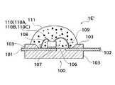
すなわち、本実施形態の発光装置1Aは、樹脂ステム100と、その上にマウントされた半導体発光素子106と、素子106を覆うように設けられた封止体111と、を有する。
【0028】
封止樹脂ステム100は、リードフレームから形成したリード101、102と、これと一体的に成形されてなる樹脂部103と、を有する。リード101、102は、それぞれの一端が近接対向するように配置されている。リード101、102の他端は、互いに反対方向に延在し、樹脂部103から外部に導出されている。
【0029】
樹脂部103には開口部105が設けられ、半導体発光素子106は、その底面にマウントされている。開口部105の平面形状は、例えば略楕円形あるいは円形とすることができる。そして、素子106を取り囲む樹脂部103の内壁面は光取り出し方向に向けて傾斜し、光を反射する反射面104として作用する。
【0030】
発光素子106は、銀(Ag)ペーストなどの接着剤107によって、開口部105の底面のリード101上にマウントされている。発光素子106は、第1および第2の電極(図示せず)を有し、金(Au)線などのボンディングワイヤ108、109によって、リード101、102と、それぞれ接続されている。
【0031】
開口部105内に充填された封止体111は、蛍光体110を含有している。本発明においては、発光素子106の発光ピーク波長を例えば400nm未満とし、蛍光体110も400nm未満の1次光により励起されるものを用いることができる。また、蛍光体110は、1種類のもののみを用いてもよいが、例えば、赤色に発光する蛍光体110Aと、緑色に発光する蛍光体110Bと、青色に発光する蛍光体110Cと、を組み合わせてもよい。但し、後に詳述するように、これ以外にも多様な組み合わせが可能である。
【0032】
本発明においては、発光素子106から放出される1次光をそのまま外部に取り出さずに、蛍光体110によって波長変換してから取り出す。つまり、発光素子106から放出された紫外光などの光は、蛍光体110(例えば、赤色蛍光体110A、緑色蛍光体110B、青色蛍光体110C)により波長変換されてそれら2次光の混合色として取り出される。
【0033】
このようにすると、発光素子106と蛍光体110の発光特性の「ずれ」や「ばらつき」による変色などの問題を解消することができる。例えば、発光素子106の波長が素子毎にばらついたり、温度条件や経年変化などの要因によって発光素子106の波長がシフトしても、それが各蛍光体に与える影響は微小であり、蛍光体から得られる混合色のバランスは殆ど変化しない。その結果として、幅広い温度範囲、幅広い動作時間範囲に亘って、発光特性が極めて安定した発光装置を実現することができる。
【0034】
また、本発明においては、例えば、赤色蛍光体110Aと、緑色蛍光体110Bと、青色蛍光体110Cとを組み合わせた3色混合型の蛍光体を透明な樹脂に含有させた場合、封止体111は「白色」の色調を有する。つまり、非点灯時に「白色」であり、点灯すると白色光を放出する点で、「見栄え」が良く各種の用途に応用するに際して視覚的に極めて有利である。
【0035】
さて、本発明は、封止体111の材料にも特徴を有する。すなわち、その材料として、従来のエポキシ樹脂に代わってシリコーン樹脂を用いると、発光ピーク波長が400nm未満の短波長光に対しても十分な耐久性を有する。
【0036】
さらに、封止体111として硬化前の粘度が高いものを用いると、蛍光体110を混合し攪拌した後に長時間放置しても螢光体110の分散状況の変化が少なく、沈降や偏析などが抑制される。特に、複数種類の螢光体を混合した場合に蛍光体の沈降や偏析が生ずると、「色ムラ」や輝度のばらつきなどの問題が生ずるが、硬化前の粘度を調節することにより、蛍光体110が封止体111内で局所的に偏ることなく均一に分散させ、発光特性を安定させることができる。
【0037】
具体的には、発光素子106の一辺のサイズが50μm〜1000μm、厚さが10μm〜1000μm、蛍光体110混合比が1重量%〜50重量%、樹脂硬化時の粘度が100cp〜10000cpの時に、螢光体110として比重及び粒径が異なる複数の蛍光体材料を混合した場合でも、偏析などが生ずることなく、封止体111内に均一に分散され、均一に発光させることができ、色調むらが無く高輝度の発光素子が実現できた。
【0038】
以上概説したように、本発明によれば、樹脂ステムなどの実装部材100の底面に発光素子106を配置し、独特の特徴を有する封止体111に蛍光体110を分散形成することにより蛍光体粒子の比重及び粒径の違いに生じる偏析が発生しても蛍光体粒子全体を発光することができるため、色調の変動や輝度の低下を抑え歩留まり高く生産することができる。
【0039】
以下、本発明の発光装置を構成する各要素について、さらに詳細に説明する。
【0040】
(発光素子106について)
発光素子106は、有機金属気相成長法(Metal-Organic Chemical Vapor Deposition:MOCVD)や分子線エピタキシャル成長法(Molecular Beam Exitaxy:MBE)などの結晶成長法により、所定の基板上に、窒化物半導体からなる発光層を有する積層構造を形成したものである。
【0041】
さらに、窒化物半導体からなる発光層を、それよりもバンドギャップの大きい層で上下から挟んだ、いわゆる「ダブルへテロ構造」とすることが望ましい。ダブルへテロ構造により、発光波長の温度変化は−40℃から100℃までの範囲で50nm以下、電流変化は1mAから100mAの範囲で50nm以下の安定した特性を得ることができる。
【0042】
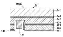
図2は、本発明において用いることができる発光素子の要部構成を模式的に表す断面図である。同図に例示した発光素子106Aは、サファイア基板121上にAlNからなるバッファ層122、n型GaNコンタクト層123、発光層を含む窒化物半導体多層膜124、p型GaAlNクラッド層125、p型GaNコンタクト層126が順次形成されている。
【0043】
この積層構造体を表面からエッチング除去されて露出したn型GaNコンタクト層123上に、Ti/Alからなるn側電極127が設けられている。一方、p型GaNコンタクト層126上には、厚さ数10nmのNi/Au薄膜からなる透光性のp側電極128、及びこれに接続された金(Au)からなるボンディングパッド129が設けられている。さらに、素子の表面は、SiO2からなる保護膜130により覆われている。
【0044】
このような発光素子106Aのn側電極127とp側電極128に電圧を印加すると、発光層124において発生した光が表面131から放出される。発光スペクトルに複数のリップルを設けることにより発光ピーク波長の強度を強くできるため、励起する螢光体の吸収が高くなり、高輝度の発光装置を実現できる。
【0045】
発光層124の半導体材料の組成(例えば、QWのウエル層の組成)を変えることによって発光波長を種々選択することができ、波長200nm以上400nm未満の紫外光が得られる。波長250nm以上400nm未満の紫外光は蛍光体の吸収が大きい点で望ましい。また、波長370nm以上400nm未満の紫外光は、発光素子106の発光効率が高い点で、さらに望ましい。さらに、波長380nm以上400nm未満の紫外光は、発光素子106を包囲する封止体111の劣化を抑えることもできる点で、またさらに望ましい。
【0046】
発光層124を、量子効果が生じる膜厚1nm〜20nmの薄膜の1層からなる単一量子井戸構造や2層以上の多重量子井戸構造とすることでスペクトル幅が狭くなり、螢光体110の励起効率が上昇する。さらに、発光層124を平面的に見て数nmから数μmのサイズのドット状に形成することにより、発光効率及び螢光体の励起効率をさらに向上させることができる。
【0047】
また、発光層124にシリコン(Si)、亜鉛(Zn)、ゲルマニウム(Ge)等の不純物を添加することによって、格子不整合に伴う歪により発生したピエゾ電界を低減でき、注入キャリアの発光再結合を促進して発光素子の発光効率を上げることができる。
【0048】
一方、基板121としては、サファイア以外に、n型GaN、n型SiC、n型ZnO、絶縁性の石英などを採用することできる。サファイアは、400nm未満の波長の透過率が高く発光層124からの発光を吸収することなく素子外部に有効に取り出すことができる。
【0049】
また、n型GaN等の導電性基板を用いた場合は、400nm未満の波長において反射率が低い金(Au)ワイヤを1本にできるため、発光層124からの発光の取り出し効率を向上させることができる。さらに、導電性基板の裏面に設けた電極によって発光層124から発光を反射して光取り出し効率を向上させることができる。また、この時に、発光素子106をマウントするための接着剤107の光による劣化も低減でき、発光装置の信頼性を上げることができる。
【0050】
サファイア基板を用いた場合、基板121上にバッファ層122、n型GaN層123を形成した後、成長温度を下げてAlNからなる第2のバッファ層を形成することで発光層124の結晶性が改善され、発光素子内の結晶欠陥が減少し、発光素子の発光効率が向上する。同時に、蛍光体110から放出された2次光の結晶欠陥における吸収も低減し、信頼性が向上するとともに発光装置の輝度が高くなる。
【0051】
バッファ層122は、AlNに限定するものではなく、GaN、AlGaN、InGaN、InGaAlNの単層、およびそれらを組合せた多層膜でもよい。厚さが数nm〜数100nmであれば、蛍光体からの発光の吸収を抑えることができ、輝度が低下することもない。
【0052】
n型層123は、GaNに限定するものではなく、AlGaN、InGaN、InGaAlからなる単層及びそれらの多層膜でもよい。その厚さを1μmから10μmの範囲にすることで、注入された電流がn型層123の内部で均一に流れ、発光素子が一様に発光し、分散している蛍光体を効率よく励起することができる。また、n型層123に添加する不純物としてシリコン(Si)、ゲルマニウム(Ge)あるいはセレン(Se)を用いると、半導体結晶の点欠陥を置換して通電による蛍光体の半導体中へのマイグレーションを抑えることができ信頼性が向上する。
【0053】
p型層125は、AlGaNに限定するものではなく、InAlGaN、InGaNの単層及びそれらの多層膜でもよい。その厚さは、数nm〜数μmの範囲であれば発光層124への注入キャリアのオーバーフローを低減でき、発光素子の発光効率が向上する。p型層125に添加する不純物としてマグネシウム(Mg)、亜鉛(Zn)を用いることにより、半導体結晶の点欠陥を置換して高温通電動作時の蛍光体の半導体中へのマイグレーションを防止できる。
【0054】
p型コンタクト層126もGaNに限定されるものではなく、AlGaN、InGaN、InGaAlNの単層及びそれらの多層膜でもよい。多層膜として膜厚数nmの複数の薄膜からなる超格子構造を用いると、p型不純物の活性化率が増加し透明電極128とのショットキー障壁が低下して接触抵抗を下げることができる。このため、発光素子周辺の蛍光体への発熱の影響を小さくでき高温まで高輝度を維持できる。
【0055】
n側電極127は、Ti/Alに限定するものではなく、スカンジウム(Sc)、イットリウム(Y)、ランタン(La)、ジルコニウム(Zr)、ハフニウム(Hf)、バナジウム(V)、ニオブ(Nb)、タンタル(Ta)、クロム(Cr)、モリブデン(Mo)、アルミニウム(Al)、金(Au)、タングステン(W)及びこれらの積層構造あるいは合金層でもよい。
【0056】
p側電極128もNi/Auに限定するものではなく、パラジウム(Pd)、白金(Pt)、コバルト(Co)、ロジウム(Rh)、イリジウム(Ir)、酸化ニッケル(NiO)、銅(Cu)、アルミニウム(Al)、マグネシウム(Mg)、酸化マグネシウム(MgO)、銀(Ag)及びこれらの積層構造あるいは合金層でもよい。
【0057】
保護膜130は、薄膜状の透光性電極128を保護するとともに通電による螢光体110の透明電極128へのマイグレーションを抑える役割も有する。その材料はSiO2に限定するものではなく、窒化シリコン(SiNx)、酸化アルミニウム(Al2O3)等の誘電体材料も用いることができる。
【0058】
図3は、本発明において用いることができる発光素子の第2の具体例を表す断面図である。すなわち、同図に表した発光素子106Bは、図2の発光素子106Aにおいてサファイア基板121の裏面側に反射膜141を設けたものである。反射膜141の材料としては、例えば、アルミニウム(Al)などの光反射率が高い材料を用いることができる。
【0059】
サファイア基板121の裏面側に設けた金属膜141は、発光層124からの発光を出射面131側に反射させ、発光素子内の発光を効率良く素子外部に取り出す機能を有する。また、発光層124からの短波長の1次光による接着剤107の変質や劣化、リード101の変色、樹脂ステム100の変色などを防止できる。接着剤107の接着強度の低下を防止する効果は大きい。さらに、金属膜141は熱伝導性が高いため放熱効果が向上し、高電流や高温動作での発光層124の発熱を発光素子外に放熱でき発熱による輝度の低下を低減できる。
【0060】
反射膜141の材料としては、アルミニウム以外にも、ニッケル(Ni)、銀(Ag)、クロム(Cr)、チタン(Ti)、銅(Cu)、金(Au)及びこれらの積層構造又は合金としてもよい。
【0061】
図4は、本発明において用いることかできる発光素子の第3の具体例を表す断面図である。すなわち、同図に表した発光素子106Cは、図2に例示した発光素子106Aにおいて透光性のp側電極128を、発光層124からの光を反射する金属層からなるp側電極161に変えたものである。このp側電極161は、例えば、膜厚が数100nm以上の金属層により構成することができる。
【0062】
発光層124からの発光はp側電極161によって反射され、サファイア基板121に吸収されることなく出射面171から取り出すことができる。本具体例の発光素子106Cは、透明電極128を用いた発光素子106A、106Bと比べて、光出力を1.5〜2倍に増加させることができ、この発光素子106Cを用いた蛍光体を含む発光装置の輝度も1.5〜2倍の高輝度化が実現できる。
【0063】
さらにp側電極161により発光層124からの発光の接着剤107への入射を防ぎ、接着剤107の劣化を抑え、さらに発光素子周辺のリード101及び樹脂ステム100の光による劣化、変色を防止できる。
【0064】
また、発光素子の発熱源のひとつである、p型層125と126における電圧降下による発熱をp側電極161を通してリード101へ発散することができる。
【0065】
同時に、発光素子106Cにおいては、これらp型層や発光層124などの発熱源を蛍光体110から遠ざけることにより、発光素子の発熱の影響を低減でき蛍光体の昇温による劣化を防止できる。その結果として、発光装置の高温動作が可能となり、信頼性も向上する。
【0066】
さらに、発光素子106Cを用いた場合には、金(Au)ワイヤを用いることなく2つのリード101、102に直接接続できる。その結果として、樹脂ストレスにともなう金(Au)ワイヤ切れなどの問題を解消することができ信頼性が向上するとともに、金ワイヤによる発光素子からの発光の吸収を解消でき高輝度が実現できる。
【0067】
また、サファイア基板121の上に成長した結晶成長層122〜126を螢光体110から離すことができ、螢光体での非発光にともなう螢光体の温度上昇の影響を受けることなく動作でき信頼性が向上する。
【0068】
p側電極161の材料としては、p型GaN層126とのショットキー障壁が小さい材料であるニッケル(Ni)、コバルト(Co)、アンチモン(Sb)、マグネシウム(Mg)、銀(Ag)、白金(Pt)、パラジウム(Pd)を用いることが望ましい。または、発光層124からの光を反射する高反射率材料であるアルミニウム(Al)、銀(Ag)を用いることが望ましい。または、接着剤107との反応が少ないモリブデン(Mo)、白金(Pt)、パラジウム(Pd)、ニッケル(Ni)、金(Au)を用いることが望ましい。
【0069】
これらの材料を多層構造とする場合には、ショットキー障壁が小さい金属膜は膜厚数nmから数10nm程度の薄膜として光の吸収を少なくし、その下に設ける高反射金属層への光の入射量を増やすようにするとよい。
【0070】
(接着剤107について)
発光素子106をリード101にマウントするために銀(Ag)などを含有するペーストを接着剤107を用いているが、Agペースト以外も用いることができる。
【0071】
Agペーストは、発光素子106とリード101との接着性が高く、温度の急激な変化に対しても強度が維持され、さらにペースト内に含まれているAgを通して効果的に放熱されるため発光層124の温度上昇を抑えることができる。またAgは、発光素子106からの1次光を反射することができ、サファイア基板121側に出射された光を光取り出し面112に反射することができる。
【0072】
Agペースト107をサファイア基板121の側面に盛り上がるように与えると、さらに接着強度が増加するとともにサファイア基板121の側面に出射した光を反射して発光素子表面131から出すことができ、高輝度が実現できる。
【0073】
接着剤107としては、Agペースト以外にも、金属を含まないシリコーン系の接着剤や波長400nm以下の光に対して透光性を有するエポキシ系接着剤、あるいは金スズ(AuSn)や金ゲルマニウム(AuGe)等の共晶合金半田など用いることもできる。
【0074】
シリコーン系接着剤は、発光による変色、接着強度の低下等が小さく信頼性が高い。
【0075】
エポキシ系接着剤は、発光による変色が生ずるため、光を反射する金属や散乱剤をいれることで変色を抑えることが望ましく、接着面側に反射膜を形成した発光素子106B、106Cと組み合わせることで信頼性の高い発光装置が実現できる。また、エポキシ系接着剤は素子をマウントするリードに対する密着性が強く発光素子の剥離が少なく、ペースト量の制御性が高い点で量産性に優れている。
【0076】
金属の共晶合金半田を利用した接着方法は、発光素子106B、106Cや、n型GaN基板等の導電性基板を用いた発光素子に対して効果が大きい。金属共晶のため接着強度が高く、発光層124の発光による変色等の劣化が無く、放熱性に優れている利点がある。しかし、接着強度が高いために高温動作時に発光素子への熱ストレスによる影響がある。これに対しては、発光素子の接着表面に、金(Au)を含有した膜厚数μm以上の金属膜を形成することによりストレスを低減できる。
【0077】
(樹脂部103について)
樹脂部103は、開口部105を有し、この開口部105の中に、発光素子106、第1及び第2のリード101、102の端部、およびツェナーダイオード(図示せず)などが設けられる。
【0078】
開口部105は、底面が狭く、上端における開口が広く、発光素子106からの1次光及び螢光体110からの発光を反射する傾斜した反射面104が底面から上端開口にわたって形成されている。
【0079】
樹脂部103は、発光素子106からの1次光及び蛍光体110で変換された光を反射する特性を有し、例えば65重量%以上の熱可塑性樹脂と充填量35重量%以下の充填剤とからなる。そして、充填剤が、酸化チタニウム(TiO2)、酸化シリコン、酸化アルミニウム、シリカ、アルミナ等の高反射性の材料を含有し、例えば、酸化チタニウムの含有量を10〜15重量%とする。このように光を反射させる拡散材を添加した樹脂部により反射面104を構成することにより、素子106及び蛍光体110からの光を上方に反射し、発光装置の高輝度が実現できる。また、反射面104の形状を回転放物線形状などとすると、さらに高出力、高品質の発光装置を提供できる。
【0080】
熱可塑性樹脂としては、液晶ポリマ(LCP)、ポリフェニレンサルファイド(PPS:熱可塑性プラスチック)、シンジオタクチックポリスチレン(SPS:結晶性ポリスチレン)などの高耐熱性樹脂を用いることができる。樹脂部103の外形の平面形状は、2.0mm×;2.0mm〜6.0mm×;6.0mm程度の略正方形、または2.0mm×;3.0mm〜5.0mm×;7.0mm程度の略長方形であり、発光素子106は凹部105の底面の中心から外れるように配置されている。このように発光素子を中心から外したのはボンディングワイヤの領域を確保するため及び発光素子106の側面近くに反射面104を形成し反射効率を高め高輝度を実現するためである。
【0081】
樹脂部103に設けられる開口部105の上面及び底面は、略円形あるいは略楕円形(長径が1mm〜2.8mmで、短径が0.5mm〜2.7mm)とすることができる。底面が狭いために、蛍光体110が均一に分散された封止体111を充填した場合、発光素子106の近傍の蛍光体量は少なく、上面ほどたくさんの蛍光体が存在する。このため、発光素子106から放出される1次光は素子の近傍から離れるに従って次第に蛍光体に吸収され2次光に変換される割合が高まり、最終的には実質的に全ての1次光を2次光に変換できるとともに、変換された2次光が他の蛍光体に吸収される確率も低減することができる。
【0082】
(蛍光体110について)
本発明において用いる蛍光体110は、発光素子106の発光層124から放出された400nm未満の紫外光を吸収して発光する蛍光体、あるいは他の蛍光体から放出された発光を吸収して発光する材料である。蛍光体の変換効率は、1ルーメン/ワット以上であることが望ましい。
【0083】
白色発光は、赤色・緑色・青色の3原色の混合か、あるいは補色関係にある2色の混合により実現できる。3原色による白色発光は、発光素子106が放出した光を吸収して青色を放出する第1の蛍光体と、赤色を発光する第2の蛍光体と、緑色を発光する第3の蛍光体とを用いることにより実現できる。
【0084】
補色による白色発光は、例えば、発光素子106からの発光を吸収して青色を発光する第1の螢光体とその青色発光を吸収して黄色を発光する第2の螢光体とを用いるか、発光素子106からの発光を吸収して緑色を発光する第1の螢光体とその緑色光を吸収して赤色に発光する第2の螢光体を用いることにより実現できる。
【0085】
また、発光波長の変化が−40℃〜100℃の温度範囲で波長変化が50nm以下の螢光体を用いることで発光素子の温度特性に依存しない発光装置が実現できる。また発光素子106の駆動電流を1mA〜100mAで動作させたときに50nm以下の波長変化を有する螢光体を用いることで素子駆動電流に伴う発光スペクトルの変化に依存しない発光装置が実現できる。
【0086】
青色光を発光する螢光体としては、例えば以下のものを挙げることができる。
ZnS:Ag
ZnS:Ag+Pigment
ZnS:Ag,Al
ZnS:Ag,Cu,Ga,Cl
ZnS:Ag+In2O3
ZnS:Zn+In2O3
(Ba,Eu)MgAl10O17
(Sr,Ca,Ba,Mg)10(PO4)6Cl2:Eu
Sr10(PO4)6Cl2:Eu
(Ba,Sr,Eu)(Mg,Mn)Al10O17
10(Sr,Ca,Ba,Eu)・6PO4・Cl2
BaMg2Al16O25:Eu
緑色光を発光する螢光体としては,例えば以下のものを挙げることができる。
ZnS:Cu,Al
ZnS:Cu,Al+Pigment
(Zn,Cd)S:Cu,Al
ZnS:Cu,Au,Al,+pigment
Y3Al5O12:Tb
Y3(Al,Ga)5O12:Tb
Y2SiO5:Tb
Zn2SiO4:Mn
(Zn,Cd)S:Cu
ZnS:Cu
Zn2SiO4:Mn
ZnS:Cu+Zn2SiO4:Mn
Gd2O2S:Tb
(Zn,Cd)S:Ag
ZnS:Cu,Al
Y2O2S:Tb
ZnS:Cu,Al+In2O3
(Zn,Cd)S:Ag+In2O3,
(Zn,Mn)2SiO4
BaAl12O19:Mn
(Ba,Sr,Mg)O・aAl2O3:Mn
LaPO4:Ce,Tb
Zn2SiO4:Mn
ZnS:Cu
3(Ba,Mg,Eu,Mn)O・8Al2O3
La2O3・0.2SiO2・0.9P2O5:Ce,Tb
CeMgAl11O19:Tb
赤色光を発光する螢光体としては、例えば次のものを用いることができる。
Y2O2S:Eu
Y2O2S:Eu+pigment
Y2O3:Eu
Zn3(PO4)2:Mn
(Zn,Cd)S:Ag+In2O3
(Y,Gd,Eu)BO3
(Y,Gd,Eu)2O3
YVO4:Eu
La2O2S:Eu,Sm
黄色光を発光する螢光体としては、例えば次のものを用いることができる。
YAG:Ce
上記したような赤色螢光体、緑色螢光体及び青色螢光体について、それらの重量比R:G:Bを調節することにより、任意の色調を実現できる。例えば、白色電球色から白色蛍光灯色までの白色発光は、R:G:B重量比が、1:1:1〜7:1:1及び1:1:1〜1:3:1及び1:1:1〜1:1:3のいずれかとすることで実現できる。
【0087】
また、混合した螢光体の総重量比を螢光体を含有する封止体の重量に対して1重量%〜50重量%にすることで実質的な波長変換が実現でき、10重量%〜30重量%にすることで高輝度の発光装置が実現できる。
【0088】
さらに、これらのRGB蛍光体を適宜選択して配合した場合、封止体111の色調を白色とすることができる。つまり、白色に光る発光装置が、非点灯時においても白色に見える点で、「見栄え」が良く、視覚的、デザイン的にも優れた発光装置を提供することができる。
【0089】
ここで、本発明において用いる螢光体は上記した無機螢光体に限定するものではなく、以下に例示する有機色素体も同様に用いて高輝度の発光装置を実現できる。
キサニセン系色素
オキサジン系色素
シアニン系色素
ローダミンB(630nm)
クマリン153(535nm)
ポリパラフェニレンビニレン(510nm)
クマリン1(430nm)
クマリン120(450nm)
トリスー(8−ヒドロキシノリン)アルミニウム(Alq3又はAlQ)(緑色発光)
4−ジシアノメチレン−2−メチル−6(p−ジメチルアミノスチリン)−4H−ピラン(DCM)(オレンジ色/赤色発光)
複数種類の色素体を用いる場合でも、封止体であるシリコーン樹脂にそれぞれの色素体を添加して攪拌することによりそれぞれの色素を樹脂中にほぼ均一に分散させることができ、色素の励起効率を高くすることができる。
【0090】
本発明によれば、発光装置の発光色は、封止体111に含有させる螢光体(色素体も含む)110の組み合わせにより多種多様のものが実現できる。つまり、赤色、緑色、青色、および黄色系などの蛍光体(色素体も含む)を配合することで任意の色調が実現できる。
【0091】
一方、本発明によれば、単一の蛍光体を用いた場合でも、従来の半導体発光素子では実現できなかった発光波長の安定性が実現できる。すなわち、通常の半導体発光素子は、駆動電流や周囲温度や変調条件などに応じて発光波長がシフトする傾向を有する。これに対して、本発明の発光装置によれば、発光波長が駆動電流や温度などの変化に依存せず、極めて安定するという効果が得られる。
【0092】
また、本発明の発光装置においては、発光特性が発光素子106の特性に依存することなく添加する蛍光体110の特性で決まるため、発光装置ごとの特性が安定し歩留まり高く生産することができる。
【0093】
(封止体111の表面形状について)
封止体111は、開口部105の中に設けられ、発光素子106からの1次光を変換する蛍光体110を含む部材である。このため、封止体111は、発光素子106からの1次光のエネルギーよりも大きな結合エネルギーを有する材料からなることが望ましく、さらに、発光素子106からの1次光を透過し、蛍光体110により波長変換された発光も透過する特性を有するものであることが望ましい。
【0094】
本発明者は、封止体111に関して独自の試作検討を行った結果、その表面形状ついて新たな知見を得た。
【0095】
図5は、封止体の表面の形状による放出光の強度分布を表す概念図である。すわち、同図(a)は封止体111の表面がほぼ平坦な場合、同図(b)は封止体111の表面が凹状に窪んで形成された場合、同図(c)は封止体111の表面が凸状に膨らんで形成された場合の発光装置からの放出光の強度分布Pをそれぞれ表す。
【0096】
図5(a)に例示した平面形状の場合と比べて、同図(b)に表した凹状の場合には放出光の強度分布すなわち配光特性は、垂直軸Z方向に収束していることが分かる。これに対して、同図(c)に表した凸状の場合には、放出光はxy平面方向に広がった配光特性を有する。これは、封止体111を凸状に形成した場合には、その凸部付近に含有される蛍光体から放出された光がxy平面方向に拡がるのに対して、凹状に形成した場合には封止体の表面付近に含有される蛍光体から放出された光も側壁の反射面104により反射されてz軸方向に進む割合が増加するためであると考えられる。
【0097】
ここで、封止体111の表面形状を凸状とするか、それとも凹状とするかは、その充填量により調節することができる。つまり、封止体111の充填量を調節することにより、所望する放出光の配光特性を得ることが可能である。
【0098】
但し、通常は、収束性が高く、z軸上において輝度が高い発光装置が要求される場合が多い。封止体111の表面を凹状に形成すれば、このような要求に確実かつ容易に応ずることができる。
【0099】
また、平面型画像表示装置のように複数の発光装置を並列配置する場合に、封止体111の表面が凸状に形成されていると、凸部の蛍光体が、隣接する発光装置からの発光を受けて不必要な励起発光を生ずる虞がある。従って、このような用途においても、封止体111の表面は凹状とすることが望ましい。
【0100】
本発明によれば、これらの要求に対しても、封止体111の充填量を調節することにより、確実かつ容易に応ずることができる。
【0101】
(封止体111の材質について)
封止体111は、発光素子106からの1次光を変換する蛍光体110を含む部材である。このため、封止体111は、発光素子106からの1次光のエネルギーよりも大きな結合をエネルギーを有する材料からなることが望ましく、さらに、発光素子106からの1次光を透過し、蛍光体110により波長変換された発光も透過する特性を有するものであることが望ましい。
【0102】
しかし、発光素子106の発光ピーク波長を400nm未満とした場合に、封止体111の材料として従来のエポキシ樹脂を用いると急速に劣化が生ずる。具体的には、発光素子からの1次光を受けると、当初は透明なエポキシ樹脂が変色し、黄色から茶褐色さらには黒色になる。その結果として、光の取り出し効率が大幅に低下するという問題が生ずることが判明した。
【0103】
これに対して、本発明者は、独自の試作検討の結果、シリコーン樹脂を用いると極めて良好な結果が得られることを知得した。すなわち、シリコーン樹脂を用いた場合、ピーク波長が400nm未満の短波長光を長期間照射しても、変色などの劣化は殆ど生じない。その結果として、短波長光を1次光とした発光装置に用いて、高い信頼性を実現することができた。
【0104】
すなわち、シリコーン樹脂は、発光素子106からの1次光及び螢光体110からの発光を透過する特性を有し、1000時間動作後の発光装置の光度が初期光度に比べて60%以上保持する特性を有している。
【0105】
ここで、蛍光体110を含有したシリコーン樹脂は、所定の(複数の)蛍光体110を混合、攪拌しながら開口の狭いノズルを通して、開口部105にマウントされた発光素子106の上に塗布される。しかる後に、硬化させて形成する。
【0106】
この際に、特に硬化前の粘度が100cp〜10000cpのシリコーン樹脂を用いると、蛍光体が樹脂内に均一に分散された後に、沈降や偏析を生ずることがない。このため、励起された蛍光体から放出された発光が他の蛍光体で過度に散乱、吸収されること無く、屈折率の大きな蛍光体で適度に均一に散乱され、光の混合も均一に生ずるため色調の「むら」も抑制できる。
【0107】
さらに、本発明において用いるシリコーン樹脂は、樹脂部103との付着強度も強く、耐湿性が高く温度ストレスによるクラック等も少ない。また、シリコーン樹脂を充填することにより周囲の温度変化による発光素子106およびAuワイヤに対する樹脂ストレスを著しく軽減させることができる。
【0108】
本発明者は、この観点からさらに検討を進めた結果、シリコーン樹脂の中でも、硬度が高い「ゴム状」のシリコーン樹脂を用いると優れた結果が得られることを見出した。すなわち、シリコーン樹脂としては、通常は、JIS規格の硬度であるJISA硬度値がおよそ30〜40のものが広く知られている。これは、「ゲル状」に近い物性を有し、物理的に柔らかいものである。以下、このシリコーン樹脂を「ゲル状シリコーン樹脂」と称する。
【0109】
これに対して、「ゴム状シリコーン樹脂」は、JISA硬度がおよそ50〜90の範囲にある。ちなみに、従来の発光装置の封止体材料として広く用いられているエポキシ樹脂は、JISA硬度がおよそ95前後である。
【0110】
本発明者は、「ゴム状シリコーン樹脂」と「ゲル状シリコーン樹脂」とを独自に比較検討した結果、以下の知見を得た。
【0111】
(1)ゲル状シリコーンを用いた場合、通電動作中に蛍光体110が樹脂中を拡散し、色調が変化する現象が見られた。RGB3色混合型の場合、赤色(R)蛍光体の比重が大きいため、この蛍光体が鉛直下方にマイグレートし、色度座標のx値が大きくなる現象が見られた。
【0112】
図6は、通電時間に対して色度xの変化を測定した結果を表すグラフである。同図に表したように、封止体111の材料としてゲル状シリコーン樹脂を用いた場合、通電時間が100時間付近から色度xが上昇し始め、1000時間を超えると加速度的に上昇する。これに対して、ゴム状のシリコーン樹脂を用いた場合は、通電動作により発光装置の温度が上昇した状態で10000時間近く動作させても、色調の変化は観察されなかった。これは、ゴム状のシリコーン樹脂の場合は、硬度が高く緻密なため、蛍光体の拡散が生じにくいためであると考えられる。
【0113】
(2)ゲル状のシリコーン樹脂は柔らかいため、発光素子106やワイア108、109に与えるストレスは小さい反面、外力に対して弱いという欠点を有する。すなわち、図1に例示したような発光装置は、例えば「表面実装型」のランプとして用いられ、アセンブリ装置により実装基板などにマウントされる。この際に、アセンブリ装置の吸着コレットが封止体111の表面に圧接される場合が多い。JISA硬度が30〜40のゲル状シリコーン樹脂を用いた場合には、吸着コレットを押し当てることにより、封止体111が変形し、これに伴ってワイア108、109が変形したり、発光素子106にストレスが与えられる場合がある。
【0114】
これに対して、JISA硬度が50以上のゴム状シリコーン樹脂を用いた場合には、発光装置の選別やアセンブリ時における選別装置やアセンブリ装置によるシリコーン樹脂の変形を防止できる。
【0115】
以上(1)及び(2)に説明したように、ゲル状シリコーン樹脂の代わりにゴム状シリコーン樹脂を用いることにより、発光特性、信頼性、機械的強度などを大幅に改善できることが判明した。
【0116】
シリコーン樹脂の硬度を上げる方法のひとつとしては、チクソ性付与剤を添加する方法がある。
【0117】
一方、封止体111としてのシリコーン樹脂に、蛍光体110とともに、散乱剤を添加すると、発光素子106からの1次光を散乱して蛍光体に均等に当てることができるとともに、蛍光体110からの発光を散乱することにより均一な混色状態を実現できる。その結果として、より少ない量の螢光体110を用いても所望の発光特性を実現できる。
【0118】
(開口部105の内部の素子配置について)
本発明の発光装置は、波長が400nm未満という短波長の窒化物半導体からなる半導体発光素子を用いる。そして、この発光素子を用いて十分な信頼性を得るためは、保護のためのツェナー・ダイオードを並列に接続することが必要である。従って、本発明の発光装置においては、開口部105の内部の限定された空間に、発光素子106と保護用ツェナー・ダイオードとを如何に効率的に配置するかが重要なポイントである。
【0119】
図7は、本発明の発光装置の開口部内部の平面構成例を模式的に表した概念図である。
【0120】
図7に表した具体例においては、樹脂ステム100に略楕円形(略長円形)の開口部が形成されている。開口部の底面105には、一対のリード101、102の先端が設けられている。そして、リード101、102の対向面には、切り欠き部101G、102Gが設けられている。発光素子106は、リード102の先端の102Bにマウントされ、一方、ツェナー・ダイオード150は、リード101の先端の101Aにマウントされている。つまり、発光素子106とツェナー・ダイオード150とは、対角の位置にそれぞれマウントされている。
【0121】
そして、発光素子106からワイア109Bがリード101Bに接続され、またワイア109Cがリード102Aに接続されている。また、ツェナー・ダイオード150からはワイア109Aがリード102Aに接続されている。なお、ツェナー・ダイオードのもう一方の電極は、ダイオードの裏面側に形成され、リード101Aに直接、接続されている。
【0122】
図7に例示した配置パターンにおいては、まず、開口部を略楕円形とすることにより、開口面積が増加して、2つの素子106、150を収容可能なスペースが広がり、発光素子106を出来るだけ開口部105の中央寄りに配置することが可能となる。
【0123】
また、ワイアをボンディングするスペースを確保することができる。すなわち、ワイア109A〜109Cをリード101、102に接続するためには、ボンディング装置のコレットを挿入するスペースが必要である。これに対して、図7のように配置すれば、対角配置された発光素子106とツェナー・ダイオード150の片側にそれぞれボンディング・コレットを挿入するスペースが得られる。しかも、3本のワイアが交差することもない。
【0124】
また、図7に例示した配置パターンにおいては、3本のワイア109A〜109Cが、略楕円形の開口部105の形状に合わせて外周に沿うように配線されている。このように配線すると、封止体111によるストレスをさらに緩和することができる。
【0125】
以上、本発明の図1乃至図7を参照しつつ、本発明の第1の実施の形態について説明した。
【0126】
以下、本発明の変型例について説明する。
【0127】
(第2の実施の形態)
次に、本発明の第2の実施の形態について説明する。
【0128】
図8は、本発明の第2の実施の形態にかかる発光装置の要部構成を模式的に表す断面図である。同図については、図1乃至図7に関して前述したものと同様の要素には同一の符号を付して詳細な説明は省略する。
【0129】
本実施形態の発光装置1Bも、樹脂ステム100と、その上にマウントされた半導体発光素子106と、素子106を覆うように設けられた封止体111と、を有する。
【0130】
但し、本実施形態においては、蛍光体110を含有した封止体111は、発光素子106の周囲のみを覆い、その外側には、光透過性樹脂からなる第2の封止体213が設けられている。
【0131】
開口部105の底面にマウントされた発光素子106の近傍のみを、螢光体110を含有した封止体111で包囲することにより、2次光の輝度が向上する。すなわち、2次光が放出される発光部分のサイズを小さくすることにより、輝度が上昇し、さらに、反射面104による集光作用もさらに高くなる。
【0132】
また、蛍光体を含有した封止体111が、樹脂部103の側壁に囲まれて下方に小さく形成されているため、外光が侵入しにくい。つまり、外光による蛍光体110の不必要な励起を抑制することができるという効果も得られる。
【0133】
さらに、本実施形態においては、封止体111がAuワイヤ108、109の全体を包囲しているので、樹脂ストレスによる断線がなく信頼性の高い発光装置が実現できる。すなわち、ワイアの一部が第2の封止体213まで突出していると、封止体111と213との界面で生ずるストレスにより断線などが生じやすくなる。これに対して、本実施形態においては、ワイア108、109の全体が封止体111に包含されているので、断線の心配がない。
【0134】
第2の封止体213の材料として、エポキシ系樹脂またはシリコーン系樹脂を用いると、樹脂部103や封止体111との密着性が増し耐湿性が向上する。発光素子106から放出される1次光のほぼ全てが封止体111において可視光に変換されるようにすれば、第2の封止体の材料としてエポキシ樹脂を用いても、変色や劣化などの問題は生じない。
【0135】
(第3の実施の形態)
次に、本発明の第3の実施の形態について説明する。
【0136】
図9は、本発明の第3の実施の形態にかかる発光装置の要部構成を模式的に表す断面図である。同図についても、図1乃至図8に関して前述したものと同様の要素には同一の符号を付して詳細な説明は省略する。
【0137】
本実施形態の発光装置1Cも、樹脂ステム100と、その上にマウントされた半導体発光素子106と、素子106を覆うように設けられた封止体111と、を有する。
【0138】
そして、第2実施形態と同様に、蛍光110を含有した封止体111は、発光素子106の周囲のみを覆っている。但し、本実施形態においては、封止体111の外側は、開放空間とされ、さらなる封止体は設けられていない。
【0139】
本実施形態においても、開口部105の底面にマウントされた発光素子106の近傍のみを、螢光体110を含有した封止体111で包囲することにより、2次光の輝度が向上する。すなわち、2次光が放出される発光部分のサイズを小さくすることにより、輝度が上昇し、さらに、反射面104による集光作用もさらに高くなる。
【0140】
特に、本実施形態においては、略半球状の封止体111が発光点となり、その周囲を反射面104が取り囲む構成とされているので、従来のランプと同様の光学的な集光効果が得られる。
【0141】
さらに、第2実施形態と同様に、蛍光体110を含有した封止体111に外光が侵入しにくく、外光による蛍光体110の不必要な励起を抑制することができるという効果も得られる。
【0142】
また、封止体111がAuワイヤ108、109の全体を包囲しているので、樹脂ストレスによる断線がなく高い信頼性も確保することができる。
【0143】
(第4の実施の形態)
次に、本発明の第4の実施の形態について説明する。
【0144】
図10は、本発明の第4の実施の形態にかかる発光装置の要部構成を模式的に表す断面図である。同図についても、図1乃至図9に関して前述したものと同様の要素には同一の符号を付して詳細な説明は省略する。
【0145】
本実施形態の発光装置1Dは、第1実施形態のものと同様に、樹脂ステム100と、その上にマウントされた半導体発光素子106と、素子106を覆うように設けられた封止体111と、を有する。
【0146】
そして、本実施形態においては、封止体111の上に、凸状の透光体413が設けられている。このような凸状透光体413によって集光作用が得られる。透光体413の材料としては、例えば、樹脂を用いることができる。特に、エポキシ樹脂またはシリコーン樹脂を用いると、封止体111との屈折率の差を小さくすることができ、封止体111との界面での反射による損失を低減できる。
【0147】
また、透光体413の凸状形状は球面状には限定されず、必要とされる集光率あるいは光度分布に応じて適宜決定することができる。
【0148】
(第5の実施の形態)
次に、本発明の第5の実施の形態について説明する。
【0149】
図11は、本発明の第5の実施の形態にかかる発光装置の要部構成を模式的に表す断面図である。同図についても、図1乃至図10に関して前述したものと同様の要素には同一の符号を付して詳細な説明は省略する。
【0150】
本実施形態の発光装置1Eも、第1実施形態のものと同様に、樹脂ステム100と、その上にマウントされた半導体発光素子106と、素子106を覆うように設けられた封止体111と、を有する。
【0151】
但し、本実施形態においては、封止体111の周囲には樹脂部103の側壁が設けられていない。このようにすると、蛍光体110からの2次光は、上方のみでなく横方向にも放出され、広い光度分布を実現できる。従って、幅広い視野角度や幅広い放射角度が要求されるような用途に応用して好適である。
【0152】
なお、本実施形態における封止体111や樹脂ステム100の形状は図示した具体例には限定されない。例えば、図12に例示したように、封止体111を略半球状とし、また、樹脂ステム100において、樹脂部103がリード101、102を埋め込んで素子周囲に低い側壁を有するものでも良い。
【0153】
(第6の実施の形態)
次に、本発明の第6の実施の形態について説明する。
【0154】
図13は、本発明の第6の実施の形態にかかる発光装置の要部構成を模式的に表す断面図である。同図についても、図1乃至図12に関して前述したものと同様の要素には同一の符号を付して詳細な説明は省略する。
【0155】
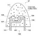
本実施形態の発光装置1Fも、リードフレームから形成した一対のリード101、102を有する。但し、第1のリード101の先端にはカップ部601が設けられ、発光素子106はカップ部601の底にマウントされている。そして、発光素子106からそれぞれのリードにワイア108、109が接続されている。さらに、これらを包囲するように蛍光体110を含有する封止体111が設けられている。
【0156】
カップ部601の内壁側面は、反射面として作用し、発光素子106から放出される1次光を上方に反射する。そして、この1次光を受けた蛍光体110が所定の波長の2次光を放出する。
【0157】
本実施形態の発光装置は、従来のランプ型半導体発光装置に代わるものであり、比較的広い放射角度を有し、汎用性の高い発光装置となる。
【0158】
(第7の実施の形態)
次に、本発明の第7の実施の形態について説明する。
【0159】
図14は、本発明の第7の実施の形態にかかる発光装置の要部構成を模式的に表す断面図である。同図についても、図1乃至図13に関して前述したものと同様の要素には同一の符号を付して詳細な説明は省略する。
【0160】
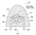
本実施形態の発光装置1Gは、第6実施形態の発光装置1Fと類似した構成を有する。すなわち、発光装置1Gも、第1のリード101の先端にカップ部601を有し、この底に発光素子106がマウントされている。そして、発光素子106からそれぞれのリードにワイア108、109が接続されている。さらに、これらを包囲するように蛍光体110を含有する封止体111が設けられている。
【0161】
但し、本実施形態においては、封止体111は小さく形成され、それを包囲するように透光体713が設けられている。
【0162】
蛍光体110を含有する封止体111を小さく形成することにより、発光部分を小さくして輝度を高くすることができる。そして、透光体713の上面がレンズ状の集光作用を有し、収束光を取り出すことも可能となる。
【0163】
また、透光体713によって封止体111を取り囲むことにより、蛍光体110を外気雰囲気から遮断し、湿気や腐食性雰囲気に対する耐久性が向上する。透光体713の材料としては樹脂を用いることができる。特に、エポキシ樹脂やシリコーン樹脂を用いると、封止体111との密着性も良好となり、優れた耐候性、機械的強度が得られる。
【0164】
なお、本実施形態も図示した具体例には限定されない。例えば、図15に例示したように、蛍光体110を含有した封止体111をカップ部601の上に限定しても良い。このようにすると、さらに発光部分が小さくなり、輝度が上昇する。この場合に、ワイア109が封止体111と透光体713との界面を貫通することとなるが、封止体111と透光体713の材料を類似したものとすれば、界面でのストレスを抑制して断線を防止することも可能である。
【0165】
以上、具体例を参照しつつ本発明の実施の形態について説明した。しかし、本発明のこれらの具体例に限定されるものではない。例えば、蛍光体の材質、発光素子の具体的な構造や材質、リードや封止体111の形状、各要素の寸法関係などに関しては、当業者が適宜設計変更したものも本発明の範囲に含まれる。
【発明の効果】
本発明は、以上説明した形態で実施され、以下に説明する効果を奏する。
すなわち、本発明によれば、波長400nm未満に強度ピークを有する1次光を放出する発光素子と、前記発光素子を覆うように設けられたシリコーン樹脂と、前記シリコーン樹脂に含有され、前記1次光を吸収して可視光を放出する蛍光体と、を備えることにより、搭載する発光素子のばらつき、駆動電流の変化、温度の変化、発光素子の劣化などによるホワイトバランスの変化を解消することが可能となる。
【0166】
また、蛍光体を適宜選択すると、非点灯時において発光面が白色の色調を有し、見栄えが良いという利点も得られる。これは実用上は大きな進歩であり、デザイン的に極めて貴重な改良点となる。
【0167】
すなわち、本発明によれば、白色などの各種の色の安定した発光が得られ、かつ見栄えも優れた発光装置を提供することが可能となり、産業上のメリットは多大である。
【図面の簡単な説明】
【図1】本発明の第1の実施の形態にかかる発光装置の要部構成を模式的に表す断面図である。
【図2】 本発明において用いることができる発光素子の要部構成を模式的に表す断面図である。
【図3】 本発明において用いることができる発光素子の第2の具体例を表す断面図である。
【図4】 本発明において用いることができる発光素子の第3の具体例を表す断面図である。
【図5】封止体の表面の形状による放出光の強度分布を表す概念図である。
【図6】通電時間に対して色度xの変化を測定した結果を表すグラフである。
【図7】本発明は発光装置の開口部の内部の平面構成例を模式的に表した概念図である。
【図8】本発明の第2の実施の形態にかかる発光装置の要部構成を模式的に表す断面図である。
【図9】本発明の第3の実施の形態にかかる発光装置の要部構成を模式的に表す断面図である。
【図10】 本発明の第4の実施の形態にかかる発光装置の要部構成を模式的に表す断面図である。
【図11】本発明の第5の実施の形態にかかる発光装置の要部構成を模式的に表す断面図である。
【図12】本発明の第5実施形態の変型例を表す断面図である。
【図13】本発明の第6の実施の形態にかかる発光装置の要部構成を模式的に表す断面図である。
【図14】 本発明の第7の実施の形態にかかる発光装置の要部構成を模式的に表す断面図である。
【図15】本発明の第7実施形態の変型例を表す断面図である。
【図16】従来の発光装置の概略構成を表す断面図である。
【符号の説明】
1A〜1G 発光装置
100 樹脂ステム
101、102 リード
103 樹脂部
104 反射面
105 開口部
106、106A〜106C 半導体発光素子
107 接着剤
108、109 ボンディングワイヤ
110、110A〜110C 螢光体
111 封止体(シリコーン樹脂)
121 光取り出し面
120 発光素子
121 基板
122 バッファ層
123 コンタクト層
124 発光層
125 クラッド層
126 コンタクト層
127 n側電極
128 p側電極
129 ボンディングパッド
130 保護膜
131 光取り出し面
141 反射膜
213 第2の封止体[0001]
BACKGROUND OF THE INVENTION
The present invention relates to a method for manufacturing a light emitting device, and more particularly to a method for manufacturing a light emitting device in which a light emitting element such as a semiconductor light emitting element and a wavelength conversion means such as a phosphor are combined.
[Prior art]
2. Description of the Related Art A light emitting device in which a semiconductor light emitting element such as an LED (Light Emitting Diode) and a phosphor are combined has been attracting attention as an inexpensive and long-life light emitting device, and its development is being promoted. In addition, this light emitting device has an advantage that it can provide an emission color that cannot be realized by a conventional semiconductor light emitting element.
[0002]
Usually, a semiconductor light emitting element emits light when carriers injected into an active layer recombine, and the emission wavelength is determined by the band gap of the active layer. For example, red and yellow are realized in a semiconductor light emitting element using an InGaAlP-based material, and green and blue single colors are realized in a semiconductor light emitting element using an InGaN-based material.
[0003]
However, in order to achieve a predetermined color mixture using such a conventional semiconductor light emitting element, the light output of each light emitting element is adjusted by combining a plurality of light emitting elements of different colors and adjusting their current values. Therefore, the configuration is complicated and adjustment is troublesome.
[0004]
On the other hand, in the case of a light emitting device that emits light by converting the wavelength of light emitted from a semiconductor light emitting element by using a phosphor material, an unprecedented emission color can be obtained by changing the type and combination of phosphor materials. This is advantageous in that it can be realized using a semiconductor light emitting element.
[0005]
As a light emitting device combining a semiconductor light emitting element and a phosphor, a white light emitting device described in Compound Semiconductor Vol. 5 No. 4 pp. 28-31 can be given. This light-emitting device realizes white light emission by mixing two colors of a semiconductor light-emitting element that emits blue light and a YAG: Ce phosphor that is excited by the blue light and emits yellow light.
[0006]
FIG. 16 is a cross-sectional view illustrating a schematic configuration of such a conventional light emitting device. That is, an opening 801 is formed in the package (resin stem) 800, a semiconductor
[0007]
The
[0008]
The light-emitting device illustrated in FIG. 16 emits white light by mixing two colors of blue light emitted from the semiconductor light-emitting
[0009]
[Problems to be solved by the invention]
However, as a result of the study by the present inventors, it has been found that the light emitting device illustrated in FIG. 16 has the following problems. That is,
(1) There is a large variation in white balance between devices.
(2) The change in white balance due to the change in the supplied current value is large.
(3) The change in white balance due to fluctuations in ambient temperature is large.
(4) A change in white balance due to a change with time of the semiconductor
These problems are all due to the essential characteristics of the blue
[0010]
If the wavelength of the blue light emitted from the blue
[0011]
Further, in the case of the light emitting device illustrated in FIG. 16, there is a problem that it is difficult to adjust the amount of phosphor in the resin including the semiconductor element in accordance with the luminance of the light emitting element. In particular, light emission from YAG: Ce with high visible sensitivity is difficult to control because an error in the amount of several μg of the phosphor affects the color tone and luminance.
[0012]
Furthermore, this light-emitting device is limited to a narrow range of usable temperatures. For example, when operated at a high temperature of 50 ° C. or higher, the color tone changes to bluish white. Such discoloration due to temperature is due to the difference between the temperature characteristics of the semiconductor element and the phosphor, and the decrease in the luminous efficiency of the phosphor at a high temperature is greater than the decrease in the luminous efficiency of the semiconductor. Has occurred.
[0013]
Furthermore, in the case of the light emitting device illustrated in FIG. 16, the
[0014]
The present invention has been made based on recognition of such problems. That is, the purpose is to manufacture a light-emitting device that suppresses variations in luminance and color tone in a light-emitting device that combines a light-emitting element and a phosphor, has a small temperature change in light-emitting characteristics, has good appearance, and has high mass productivity and reproducibility It is to provide a method.
[0015]
[Means for Solving the Problems]
In order to achieve the above object, according to one embodiment of the present invention, a light-emitting element that emits primary light having a peak wavelength of less than 400 nm and a surface of a light-emitting device that covers the light-emitting element are formed. A silicone resin; a first phosphor contained in the silicone resin that absorbs the primary light and emits first visible light; and a silicone resin contained in the silicone resin that absorbs the primary light and absorbs the first light. Emits second visible light with a wavelength different from that of visible lightThe specific gravity and the particle size are different from those of the first phosphor.The second phosphor is a method for manufacturing a light emitting device, wherein the light emission is performed by a silicone resin containing the first phosphor and the second phosphor and having a viscosity before curing of 100 to 10,000 cp. A method of manufacturing a light emitting device is provided, which covers an element and cures the silicone resin to a hardness of 50 or more in terms of JIS value.
According to another aspect of the present invention, a light emitting element that emits primary light, a silicone resin that covers the light emitting element so as to form a surface of a light emitting device, and the silicone resin are included. A first phosphor that absorbs the primary light and emits first visible light; and a second phosphor that is contained in the silicone resin and absorbs the primary light and has a wavelength different from that of the first visible light. Emitting visible lightThe specific gravity and the particle size are different from those of the first phosphor.A second phosphor, and a silicone resin having a viscosity before curing of 100 to 10000 cp, wherein 1 wt% to 50 wt% of the first and second phosphors are mixed. Then, a method for manufacturing a light-emitting device is provided, which covers the light-emitting element and hardens the silicone resin to a hardness of 50 or more in terms of JIS value.
[0016]
By using such a unique silicone resin as a sealing body, it is possible to realize a wavelength conversion type light emitting device excellent in light resistance, weather resistance, and mechanical durability.
[0017]
Here, when the primary light emitted from the light-emitting element has an intensity peak below a wavelength of 400 nm, the phosphor absorbs the primary light with high efficiency and converts the wavelength to obtain a high light output. .
[0018]
Further, as the phosphor, a first phosphor that absorbs the primary light and emits first visible light, and a first phosphor that absorbs the primary light and has a wavelength different from that of the first visible light. An arbitrary mixed color can be realized by using the second phosphor that emits two visible lights.
[0019]
Further, if the first visible light and the second visible light are in a complementary color relationship, for example, blue and yellow, or red and blue-green are mixed to emit white light. Obtainable.
[0020]
Alternatively, as the phosphor, a first phosphor that absorbs the primary light and emits red light, a second phosphor that absorbs the primary light and emits green light, and the primary If a third phosphor that absorbs light and emits blue light is used, substantially white light can be obtained by mixing the red light, green light, and blue light.
[0021]
Further, if the wire further includes a wire connected to the light emitting element, and the silicone resin is provided so as to cover the wire, the wire and the wire are protected by a sealing body, and the wire is disconnected or deformed. Can be suppressed.
[0022]
Further, if a resin part having an opening is further provided, the light emitting element is disposed at the bottom of the opening, and the silicone resin is provided in the opening, various light emitting devices such as a so-called surface mount type are provided. Can be realized.
[0023]
In the present application, “silicone resin” refers to a resin having as a skeleton a structure in which silicon atoms having organic groups such as alkyl groups and aryl groups are alternately bonded to oxygen atoms. Of course, the “silicone resin” includes those having other additive elements added to the skeleton.
[0024]
Further, in the present application, the “phosphor” includes those having a wavelength converting action, and includes, for example, not only an inorganic phosphor but also an organic phosphor or an organic dye having a wavelength converting action.
[0025]
Further, in the present application, “nitride semiconductor” means BxInyAlzGa(1-xyz)N (0.ltoreq.x.ltoreq.1, 0.ltoreq.y.ltoreq.1, 0.ltoreq.z.ltoreq.1, 0.ltoreq.x + y + z.ltoreq.1) III-V group compound semiconductors. Further, as a group V element, in addition to N (nitrogen) And mixed crystals containing phosphorus (P), arsenic (As), and the like.
DETAILED DESCRIPTION OF THE INVENTION
The present invention provides a light-emitting device that emits short-wavelength primary light emitted from a semiconductor light-emitting element by converting the wavelength with a phosphor and emits light with excellent wavelength stability and reproducibility of light emission characteristics. Is.
[0026]
Hereinafter, embodiments of the present invention will be described with reference to the drawings.
(First embodiment)
FIG. 1 is a cross-sectional view schematically showing the main configuration of the light emitting device according to the first embodiment of the present invention.
[0027]
That is, the
[0028]
The sealing
[0029]
The
[0030]
The
[0031]
The sealing
[0032]
In the present invention, the primary light emitted from the
[0033]
By doing so, problems such as discoloration due to “deviation” or “variation” in the light emission characteristics of the
[0034]
In the present invention, for example, when a three-color mixed phosphor obtained by combining the
[0035]
The present invention is also characterized by the material of the sealing
[0036]
Further, when a sealing
[0037]
Specifically, when the size of one side of the
[0038]
As outlined above, according to the present invention, the
[0039]
Hereafter, each element which comprises the light-emitting device of this invention is demonstrated in detail.
[0040]
(About Light Emitting Element 106)
The light-emitting
[0041]
Furthermore, it is desirable to have a so-called “double hetero structure” in which a light emitting layer made of a nitride semiconductor is sandwiched from above and below by a layer having a larger band gap. Due to the double hetero structure, it is possible to obtain stable characteristics in which the temperature change of the emission wavelength is 50 nm or less in the range from −40 ° C. to 100 ° C., and the current change is 50 nm or less in the range of 1 mA to 100 mA.
[0042]
FIG. 2 is a cross-sectional view schematically showing a main configuration of a light-emitting element that can be used in the present invention. The light-emitting
[0043]
An n-
[0044]
When voltage is applied to the n-
[0045]
By changing the composition of the semiconductor material of the light emitting layer 124 (for example, the composition of the QW well layer), various emission wavelengths can be selected, and ultraviolet light having a wavelength of 200 nm or more and less than 400 nm can be obtained. Ultraviolet light having a wavelength of 250 nm or more and less than 400 nm is desirable because of the large absorption of the phosphor. In addition, ultraviolet light having a wavelength of 370 nm or more and less than 400 nm is more preferable in terms of high luminous efficiency of the
[0046]
By making the light emitting layer 124 a single quantum well structure or a multiple quantum well structure of two or more layers having a thin film thickness of 1 nm to 20 nm in which the quantum effect occurs, the spectral width is narrowed. Excitation efficiency increases. Furthermore, when the
[0047]
Further, by adding impurities such as silicon (Si), zinc (Zn), germanium (Ge), etc. to the
[0048]
On the other hand, as the
[0049]
In addition, when a conductive substrate such as n-type GaN is used, a single gold (Au) wire having a low reflectance at a wavelength of less than 400 nm can be formed, so that the light extraction efficiency from the
[0050]
When a sapphire substrate is used, after the
[0051]
The
[0052]
The n-
[0053]
The p-
[0054]
The p-
[0055]
The n-
[0056]
The p-
[0057]
The
[0058]
FIG. 3 is a cross-sectional view illustrating a second specific example of a light-emitting element that can be used in the present invention. That is, the light-emitting
[0059]
The
[0060]
As a material of the
[0061]
FIG. 4 is a cross-sectional view illustrating a third specific example of a light-emitting element that can be used in the present invention. That is, the light-emitting
[0062]
Light emitted from the
[0063]
Further, the p-
[0064]
Further, heat generated by a voltage drop in the p-
[0065]
At the same time, in the
[0066]
Further, when the
[0067]
Further, the crystal growth layers 122 to 126 grown on the
[0068]
As the material of the p-
[0069]
When these materials have a multi-layer structure, a metal film having a small Schottky barrier is a thin film with a film thickness of several nanometers to several tens of nanometers so that light absorption is reduced, and the light reflected on the highly reflective metal layer provided thereunder is reduced. It is preferable to increase the amount of incident light.
[0070]
(About adhesive 107)
In order to mount the
[0071]
The Ag paste has high adhesiveness between the light emitting
[0072]
When the
[0073]
As the adhesive 107, in addition to the Ag paste, a silicone-based adhesive that does not contain a metal, an epoxy-based adhesive that transmits light with a wavelength of 400 nm or less, gold tin (AuSn), or gold germanium ( A eutectic alloy solder such as AuGe) can also be used.
[0074]
Silicone adhesives are small in discoloration due to light emission, decrease in adhesive strength, and the like, and are highly reliable.
[0075]
Epoxy adhesives cause discoloration due to light emission, so it is desirable to suppress discoloration by adding a metal that reflects light or a scattering agent, and in combination with light emitting
[0076]
The bonding method using a metal eutectic alloy solder has a great effect on the
[0077]
(Resin part 103)
The
[0078]
The
[0079]
The
[0080]
As the thermoplastic resin, a high heat-resistant resin such as liquid crystal polymer (LCP), polyphenylene sulfide (PPS: thermoplastic plastic), or syndiotactic polystyrene (SPS: crystalline polystyrene) can be used. The planar shape of the outer shape of the
[0081]
The upper surface and the bottom surface of the
[0082]
(About phosphor 110)
The
[0083]
White light emission can be realized by mixing three primary colors of red, green, and blue, or by mixing two colors that are complementary. The white light emission by the three primary colors is a first phosphor that absorbs light emitted from the
[0084]
For complementary white light emission, for example, is the first phosphor that absorbs light emitted from the
[0085]
In addition, a light-emitting device that does not depend on the temperature characteristics of the light-emitting element can be realized by using a phosphor having a light emission wavelength change of −40 ° C. to 100 ° C. and a wavelength change of 50 nm or less. Further, by using a phosphor having a wavelength change of 50 nm or less when the drive current of the light-emitting
[0086]
Examples of the phosphor that emits blue light include the following.
ZnS: Ag
ZnS: Ag + Pigment
ZnS: Ag, Al
ZnS: Ag, Cu, Ga, Cl
ZnS: Ag + In2O3
ZnS: Zn + In2O3
(Ba, Eu) MgAl10O17
(Sr, Ca, Ba, Mg)10(PO4)6Cl2: Eu
Sr10(PO4)6Cl2: Eu
(Ba, Sr, Eu) (Mg, Mn) Al10O17
10 (Sr, Ca, Ba, Eu) · 6PO4・ Cl2
BaMg2Al16O25: Eu
Examples of the phosphor that emits green light include the following.
ZnS: Cu, Al
ZnS: Cu, Al + Pigment
(Zn, Cd) S: Cu, Al
ZnS: Cu, Au, Al, + pigment
Y3Al5O12: Tb
Y3(Al, Ga)5O12: Tb
Y2SiO5: Tb
Zn2SiO4: Mn
(Zn, Cd) S: Cu
ZnS: Cu
Zn2SiO4: Mn
ZnS: Cu + Zn2SiO4: Mn
Gd2O2S: Tb
(Zn, Cd) S: Ag
ZnS: Cu, Al
Y2O2S: Tb
ZnS: Cu, Al + In2O3
(Zn, Cd) S: Ag + In2O3,
(Zn, Mn)2SiO4
BaAl12O19: Mn
(Ba, Sr, Mg) O · aAl2O3: Mn
LaPO4: Ce, Tb
Zn2SiO4: Mn
ZnS: Cu
3 (Ba, Mg, Eu, Mn) O · 8Al2O3
La2O3・ 0.2SiO2・ 0.9P2O5: Ce, Tb
CeMgAl11O19: Tb
As the phosphor that emits red light, for example, the following can be used.
Y2O2S: Eu
Y2O2S: Eu + pigment
Y2O3: Eu
Zn3(PO4)2: Mn
(Zn, Cd) S: Ag + In2O3
(Y, Gd, Eu) BO3
(Y, Gd, Eu)2O3
YVO4: Eu
La2O2S: Eu, Sm
As the phosphor that emits yellow light, for example, the following can be used.
YAG: Ce
By adjusting the weight ratio R: G: B of the red phosphor, the green phosphor and the blue phosphor as described above, an arbitrary color tone can be realized. For example, white light emission from a white light bulb color to a white fluorescent light color has R: G: B weight ratios of 1: 1: 1 to 7: 1: 1 and 1: 1: 1 to 1: 3: 1 and 1. It can be realized by setting one of 1: 1 to 1: 1: 3.
[0087]
Moreover, substantial wavelength conversion can be realized by setting the total weight ratio of the mixed phosphor to 1 to 50% by weight with respect to the weight of the sealing body containing the phosphor. By setting the content to 30% by weight, a light emitting device with high luminance can be realized.
[0088]
Furthermore, when these RGB phosphors are appropriately selected and blended, the color tone of the sealing
[0089]
Here, the phosphor used in the present invention is not limited to the inorganic phosphor described above, and a high-luminance light-emitting device can be realized using the organic pigments exemplified below as well.
Xanicene dyes
Oxazine dye
Cyanine dye
Rhodamine B (630nm)
Coumarin 153 (535nm)
Polyparaphenylene vinylene (510nm)
Coumarin 1 (430nm)
Coumarin 120 (450nm)
Tris (8-hydroxynoline) aluminum (Alq3 or AlQ) (green light emission)
4-Dicyanomethylene-2-methyl-6 (p-dimethylaminostyrin) -4H-pyran (DCM) (orange / red emission)
Even when multiple types of pigments are used, the pigments can be dispersed almost uniformly in the resin by adding the pigments to the silicone resin that is the sealant and stirring them. Can be high.
[0090]
According to the present invention, a wide variety of emission colors of the light emitting device can be realized by combining the phosphors (including pigment bodies) 110 contained in the sealing
[0091]
On the other hand, according to the present invention, even when a single phosphor is used, stability of the emission wavelength that cannot be realized by a conventional semiconductor light emitting device can be realized. That is, a normal semiconductor light emitting element has a tendency that the emission wavelength shifts according to the drive current, the ambient temperature, the modulation condition, and the like. On the other hand, according to the light emitting device of the present invention, it is possible to obtain an effect that the emission wavelength is extremely stable without depending on changes in driving current, temperature, and the like.
[0092]
Further, in the light emitting device of the present invention, since the light emission characteristics are determined by the characteristics of the
[0093]
(About the surface shape of the sealing body 111)
The sealing
[0094]
The present inventor obtained a new knowledge about the surface shape as a result of conducting an original prototype study on the sealing
[0095]
FIG. 5 is a conceptual diagram showing the intensity distribution of emitted light according to the shape of the surface of the sealing body. That is, FIG. 6A shows a case where the surface of the sealing
[0096]
Compared to the planar shape illustrated in FIG. 5A, the intensity distribution of emitted light, that is, the light distribution characteristic, converges in the vertical axis Z direction in the concave shape shown in FIG. I understand. On the other hand, in the case of the convex shape shown in FIG. 5C, the emitted light has a light distribution characteristic spreading in the xy plane direction. This is because when the sealing
[0097]
Here, whether the surface shape of the sealing
[0098]
However, usually, a light emitting device with high convergence and high luminance on the z-axis is often required. If the surface of the sealing
[0099]
In addition, when a plurality of light emitting devices are arranged in parallel as in a flat-type image display device, if the surface of the sealing
[0100]
According to the present invention, it is possible to meet these requirements reliably and easily by adjusting the filling amount of the sealing
[0101]
(About the material of the sealing body 111)
The sealing
[0102]
However, when the emission peak wavelength of the light-emitting
[0103]
On the other hand, the present inventor has found out that an extremely good result can be obtained by using a silicone resin as a result of original trial production. That is, when a silicone resin is used, even when short wavelength light having a peak wavelength of less than 400 nm is irradiated for a long time, deterioration such as discoloration hardly occurs. As a result, it was possible to achieve high reliability by using a light emitting device using short wavelength light as primary light.
[0104]
That is, the silicone resin has a characteristic of transmitting the primary light from the
[0105]
Here, the silicone resin containing the
[0106]
At this time, in particular, when a silicone resin having a viscosity of 100 cp to 10000 cp before curing is used, the phosphor is not uniformly dispersed in the resin, and no sedimentation or segregation occurs. For this reason, the light emitted from the excited phosphor is not scattered and absorbed excessively by other phosphors, but is scattered moderately and uniformly by a phosphor having a large refractive index, and light is mixed evenly. Therefore, “unevenness” in color tone can also be suppressed.
[0107]
Furthermore, the silicone resin used in the present invention has high adhesion strength to the
[0108]
As a result of further investigation from this viewpoint, the present inventor has found that, among silicone resins, excellent results can be obtained by using a “rubbery” silicone resin having a high hardness. That is, as the silicone resin, those having a JIS hardness value of about 30 to 40, which is the hardness of JIS standard, are widely known. This has physical properties close to “gel” and is physically soft. Hereinafter, this silicone resin is referred to as a “gel silicone resin”.
[0109]
In contrast, the “rubbery silicone resin” has a JISA hardness in the range of about 50 to 90. Incidentally, an epoxy resin widely used as a sealing material of a conventional light emitting device has a JISA hardness of about 95.
[0110]
As a result of independent comparison and examination of “rubber-like silicone resin” and “gel-like silicone resin”, the present inventor has obtained the following knowledge.
[0111]
(1) When gel-like silicone was used, the phenomenon that the
[0112]
FIG. 6 is a graph showing the result of measuring the change in chromaticity x with respect to the energization time. As shown in the figure, when a gel-like silicone resin is used as the material of the sealing
[0113]
(2) Since the gel-like silicone resin is soft, the stress applied to the light-emitting
[0114]
On the other hand, when a rubber-like silicone resin having a JISA hardness of 50 or more is used, it is possible to prevent the silicone resin from being deformed by the sorting device or the assembly device during sorting or assembly of the light emitting device.
[0115]
As described above in (1) and (2), it has been found that the use of a rubbery silicone resin in place of the gel silicone resin can significantly improve the light emission characteristics, reliability, mechanical strength, and the like.
[0116]
One method for increasing the hardness of the silicone resin is to add a thixotropic agent.
[0117]
On the other hand, when a scattering agent is added to the silicone resin as the sealing
[0118]
(About element arrangement inside opening 105)
The light emitting device of the present invention uses a semiconductor light emitting element made of a nitride semiconductor with a short wavelength of less than 400 nm. In order to obtain sufficient reliability using this light emitting element, it is necessary to connect a Zener diode for protection in parallel. Therefore, in the light emitting device of the present invention, an important point is how to efficiently arrange the
[0119]
FIG. 7 is a conceptual diagram schematically showing a planar configuration example inside the opening of the light emitting device of the present invention.
[0120]
In the specific example shown in FIG. 7, a substantially oval (substantially oval) opening is formed in the
[0121]
From the
[0122]
In the arrangement pattern illustrated in FIG. 7, first, by making the opening substantially elliptical, the opening area is increased, and a space that can accommodate the two
[0123]
Moreover, a space for bonding wires can be secured. That is, in order to connect the
[0124]
In the arrangement pattern illustrated in FIG. 7, three
[0125]
The first embodiment of the present invention has been described above with reference to FIGS. 1 to 7 of the present invention.
[0126]
Hereinafter, modified examples of the present invention will be described.
[0127]
(Second Embodiment)
Next, a second embodiment of the present invention will be described.
[0128]
FIG. 8 is a cross-sectional view schematically showing the main configuration of the light emitting device according to the second embodiment of the present invention. In this figure, the same elements as those described above with reference to FIGS. 1 to 7 are denoted by the same reference numerals, and detailed description thereof is omitted.
[0129]
The
[0130]
However, in this embodiment, the sealing
[0131]
The brightness of the secondary light is improved by surrounding only the vicinity of the
[0132]
Moreover, since the sealing
[0133]
Furthermore, in this embodiment, since the sealing
[0134]
When an epoxy resin or a silicone resin is used as the material of the
[0135]
(Third embodiment)
Next, a third embodiment of the present invention will be described.
[0136]
FIG. 9 is a cross-sectional view schematically showing a main configuration of a light emitting device according to the third embodiment of the present invention. Also in this figure, the same elements as those described above with reference to FIGS. 1 to 8 are denoted by the same reference numerals, and detailed description thereof is omitted.
[0137]
The
[0138]
As in the second embodiment, the sealing
[0139]
Also in this embodiment, the brightness of the secondary light is improved by surrounding only the vicinity of the
[0140]
In particular, in the present embodiment, since the substantially
[0141]
Furthermore, as in the second embodiment, it is difficult for external light to enter the sealing
[0142]
Further, since the sealing
[0143]
(Fourth embodiment)
Next, a fourth embodiment of the present invention will be described.
[0144]
FIG. 10 is a cross-sectional view schematically showing a main configuration of a light emitting device according to the fourth embodiment of the present invention. Also in this figure, the same elements as those described above with reference to FIGS. 1 to 9 are denoted by the same reference numerals, and detailed description thereof is omitted.
[0145]
As in the first embodiment, the
[0146]
In the present embodiment, a convex
[0147]
Further, the convex shape of the
[0148]
(Fifth embodiment)
Next, a fifth embodiment of the present invention will be described.
[0149]
FIG. 11: is sectional drawing which represents typically the principal part structure of the light-emitting device concerning the 5th Embodiment of this invention. Also in this figure, the same elements as those described above with reference to FIGS. 1 to 10 are denoted by the same reference numerals, and detailed description thereof is omitted.
[0150]
Similarly to the
[0151]
However, in this embodiment, the side wall of the
[0152]
In addition, the shape of the sealing
[0153]
(Sixth embodiment)
Next, a sixth embodiment of the present invention will be described.
[0154]
FIG. 13: is sectional drawing which represents typically the principal part structure of the light-emitting device concerning the 6th Embodiment of this invention. Also in this figure, the same elements as those described above with reference to FIGS. 1 to 12 are denoted by the same reference numerals, and detailed description thereof is omitted.
[0155]
The
[0156]
The inner wall side surface of the
[0157]
The light-emitting device of this embodiment is an alternative to the conventional lamp-type semiconductor light-emitting device, has a relatively wide radiation angle, and becomes a highly versatile light-emitting device.
[0158]
(Seventh embodiment)
Next, a seventh embodiment of the present invention will be described.
[0159]
FIG. 14: is sectional drawing which represents typically the principal part structure of the light-emitting device concerning the 7th Embodiment of this invention. Also in this figure, the same elements as those described above with reference to FIGS. 1 to 13 are denoted by the same reference numerals, and detailed description thereof is omitted.
[0160]
The
[0161]
However, in this embodiment, the sealing
[0162]
By forming the sealing
[0163]
Further, by enclosing the sealing
[0164]
Note that this embodiment is not limited to the illustrated example. For example, as illustrated in FIG. 15, the sealing
[0165]
The embodiments of the present invention have been described above with reference to specific examples. However, it is not limited to these specific examples of the present invention. For example, regarding the material of the phosphor, the specific structure and material of the light emitting element, the shape of the lead and the sealing
【The invention's effect】
The present invention is implemented in the form described above, and has the effects described below.
That is, according to the present invention, a light emitting element that emits primary light having an intensity peak at a wavelength of less than 400 nm, a silicone resin provided to cover the light emitting element, and the silicone resin are contained in the primary resin. And a phosphor that absorbs light and emits visible light can eliminate variations in white balance due to variations in mounted light emitting elements, changes in drive current, changes in temperature, deterioration of light emitting elements, etc. It becomes possible.
[0166]
In addition, when the phosphor is appropriately selected, there is also an advantage that the light emitting surface has a white color tone when not lit and the appearance is good. This is a major advance in practical use and is an extremely valuable improvement in design.
[0167]
That is, according to the present invention, it is possible to provide a light emitting device that can stably emit light of various colors such as white and has an excellent appearance, and has a great industrial advantage.
[Brief description of the drawings]
FIG. 1 is a cross-sectional view schematically showing a configuration of a main part of a light emitting device according to a first embodiment of the invention.
FIG. 2 is a cross-sectional view schematically showing a main configuration of a light emitting element that can be used in the present invention.
FIG. 3 is a cross-sectional view illustrating a second specific example of a light-emitting element that can be used in the present invention.
FIG. 4 is a cross-sectional view illustrating a third specific example of a light-emitting element that can be used in the present invention.
FIG. 5 is a conceptual diagram showing an intensity distribution of emitted light according to a shape of a surface of a sealing body.
FIG. 6 is a graph showing a result of measuring a change in chromaticity x with respect to energization time.
FIG. 7 is a conceptual diagram schematically showing an example of a planar configuration inside an opening of a light emitting device.
FIG. 8 is a cross-sectional view schematically showing a main configuration of a light emitting apparatus according to a second embodiment of the present invention.
FIG. 9 is a cross-sectional view schematically showing a main configuration of a light emitting device according to a third embodiment of the invention.
FIG. 10 is a cross-sectional view schematically showing the main configuration of a light emitting device according to a fourth embodiment of the invention.
FIG. 11 is a cross-sectional view schematically showing a main configuration of a light emitting device according to a fifth embodiment of the invention.
FIG. 12 is a cross-sectional view illustrating a modified example of the fifth embodiment of the present invention.
FIG. 13 is a cross-sectional view schematically showing a main configuration of a light emitting device according to a sixth embodiment of the present invention.
FIG. 14 is a cross-sectional view schematically showing a configuration of a main part of a light emitting device according to a seventh embodiment of the invention.
FIG. 15 is a cross-sectional view showing a modification of the seventh embodiment of the present invention.
FIG. 16 is a cross-sectional view illustrating a schematic configuration of a conventional light emitting device.
[Explanation of symbols]
1A-1G light emitting device
100 resin stem
101, 102 lead
103 Resin part
104 Reflective surface
105 opening
106, 106A to 106C Semiconductor light emitting device
107 Adhesive
108, 109 Bonding wire
110, 110A-110C phosphor
111 Sealing body (silicone resin)
121 Light extraction surface
120 light emitting device
121 substrate
122 Buffer layer
123 Contact layer
124 light emitting layer
125 Clad layer
126 Contact layer
127 n-side electrode
128 p-side electrode
129 Bonding pad
130 Protective film
131 Light extraction surface
141 reflective film
213 Second sealing body
Claims (7)
Translated fromJapanese前記第1の蛍光体と前記第2の蛍光体とを含有し硬化前の粘度が100〜10000cpのシリコーン樹脂により前記発光素子を覆い、前記シリコーン樹脂を硬化させることによりJISA値で50以上の硬度に硬化させることを特徴とする発光装置の製造方法。A light emitting element that emits primary light having a peak wavelength of less than 400 nm, a silicone resin that covers the light emitting element and forms a surface of a light emitting device, and that is contained in the silicone resin and absorbs the primary light. a first phosphor that emits first visible light Te,the releasing second visible light having a wavelength different from said absorbs contained the primary light to the silicone resin first visible lightthe first phosphor the method for manufacturing a light emitting device having a second phosphordensity and particle size is thatDo different, a,
Hardness of 50 or more in terms of JISA value by covering the light emitting element with a silicone resin containing the first phosphor and the second phosphor and having a viscosity before curing of 100 to 10,000 cp, and curing the silicone resin. A method for manufacturing a light emitting device, characterized by being cured.
硬化前の粘度が100〜10000cpのシリコーン樹脂に1重量%〜50重量%の前記第1及び第2の蛍光体を混合して前記発光素子を覆い、前記シリコーン樹脂を硬化させることによりJISA値で50以上の硬度に硬化させることを特徴とする発光装置の製造方法。A light emitting element that emits primary light; a silicone resin that covers the light emitting element so as to form a surface of a light emitting device; and a first visible light that is contained in the silicone resin and absorbs the primary light. And a first phosphor that is contained in the silicone resin, absorbs the primary light, emits a second visible light having a wavelength different from the first visible light, andthe first phosphor. the method for manufacturing a light emitting device including a second phosphordensity and particle size is thatDo different, a,
A silicone resin having a viscosity before curing of 100 to 10000 cp is mixed with 1% to 50% by weight of the first and second phosphors to cover the light emitting element, and the silicone resin is cured to obtain a JISA value. A method for manufacturing a light-emitting device, wherein the method is cured to a hardness of 50 or more.
前記第1の可視光は、赤色光であり、
前記第2の可視光は、緑色光であり、
前記赤色光と緑色光と青色光との混色により略白色の光が得られることを特徴とする請求項1〜3のいずれか1つに記載の発光装置の製造方法。The light emitting device further includes a third phosphor that is contained in the silicone resin and absorbs the primary light to emit blue light,
The first visible light is red light;
The second visible light is green light;
Method of manufacturing a light-emitting device according to any one of claims1-3, wherein a substantially white light obtained by mixture of the said red, green, and blue light.
前記シリコーン樹脂により前記ワイアも覆うことを特徴とする請求項1〜5のいずれか1つに記載の発光装置の製造方法。The light emitting device further includes a wire connected to the light emitting element,
The method for manufacturing a light emitting device according to claim 1, wherein the wire is also covered with the silicone resin.
前記シリコーン樹脂を前記開口の中に充填することを特徴とする請求項1〜6のいずれか1つに記載の発光装置の製造方法。The light emitting element is arranged at the bottom of the resin part having an opening,
The method for manufacturing a light emitting device according to claim 1, wherein the opening is filled with the silicone resin.
Priority Applications (7)
| Application Number | Priority Date | Filing Date | Title |
|---|---|---|---|
| JP2001110673AJP4101468B2 (en) | 2001-04-09 | 2001-04-09 | Method for manufacturing light emitting device |
| EP02007366.4AEP1249873B1 (en) | 2001-04-09 | 2002-04-08 | Light emitting device |
| KR10-2002-0018973AKR100491314B1 (en) | 2001-04-09 | 2002-04-08 | Light emitting device |
| US10/118,612US7176623B2 (en) | 2001-04-09 | 2002-04-08 | Light emitting device |
| CNB021060800ACN100492679C (en) | 2001-04-09 | 2002-04-09 | light emitting device |
| CN2009101331636ACN101562225B (en) | 2001-04-09 | 2002-04-09 | Light emitting device |
| US11/608,187US7569989B2 (en) | 2001-04-09 | 2006-12-07 | Light emitting device |
Applications Claiming Priority (1)
| Application Number | Priority Date | Filing Date | Title |
|---|---|---|---|
| JP2001110673AJP4101468B2 (en) | 2001-04-09 | 2001-04-09 | Method for manufacturing light emitting device |
Publications (2)
| Publication Number | Publication Date |
|---|---|
| JP2002314142A JP2002314142A (en) | 2002-10-25 |
| JP4101468B2true JP4101468B2 (en) | 2008-06-18 |
Family
ID=18962396
Family Applications (1)
| Application Number | Title | Priority Date | Filing Date |
|---|---|---|---|
| JP2001110673AExpired - LifetimeJP4101468B2 (en) | 2001-04-09 | 2001-04-09 | Method for manufacturing light emitting device |
Country Status (5)
| Country | Link |
|---|---|
| US (2) | US7176623B2 (en) |
| EP (1) | EP1249873B1 (en) |
| JP (1) | JP4101468B2 (en) |
| KR (1) | KR100491314B1 (en) |
| CN (2) | CN101562225B (en) |
Families Citing this family (207)
| Publication number | Priority date | Publication date | Assignee | Title |
|---|---|---|---|---|
| JP4724924B2 (en)* | 2001-02-08 | 2011-07-13 | ソニー株式会社 | Manufacturing method of display device |
| JP2002314138A (en)* | 2001-04-09 | 2002-10-25 | Toshiba Corp | Light emitting device |
| JP2003078162A (en)* | 2001-08-31 | 2003-03-14 | Shin Etsu Handotai Co Ltd | GaP based semiconductor light emitting device |
| JP2003152227A (en)* | 2001-11-14 | 2003-05-23 | Citizen Electronics Co Ltd | LED color correction means and color correction method |
| JP2004253747A (en)* | 2002-02-27 | 2004-09-09 | Mitsubishi Chemicals Corp | Light emitting device and lighting device using the same |
| US20030189215A1 (en) | 2002-04-09 | 2003-10-09 | Jong-Lam Lee | Method of fabricating vertical structure leds |
| US8294172B2 (en) | 2002-04-09 | 2012-10-23 | Lg Electronics Inc. | Method of fabricating vertical devices using a metal support film |
| JP3866149B2 (en)* | 2002-05-08 | 2007-01-10 | 富士通株式会社 | Manufacturing method of semiconductor device |
| US6841802B2 (en) | 2002-06-26 | 2005-01-11 | Oriol, Inc. | Thin film light emitting diode |
| JP2004186168A (en)* | 2002-11-29 | 2004-07-02 | Shin Etsu Chem Co Ltd | Silicone resin composition for light emitting diode element |
| DE20306928U1 (en)* | 2003-01-30 | 2004-06-03 | Osram Opto Semiconductors Gmbh | Semiconductor component emitting and/or receiving radiation used as an optoelectronic semiconductor component comprises a semiconductor chip arranged in a recess of a housing base body and encapsulated with a sleeve mass |
| JP2006313943A (en)* | 2003-02-18 | 2006-11-16 | Sharp Corp | Semiconductor light emitting device, method for manufacturing the same, and electronic imaging device |
| JP3910171B2 (en)* | 2003-02-18 | 2007-04-25 | シャープ株式会社 | Semiconductor light emitting device, method for manufacturing the same, and electronic imaging device |
| KR20050113200A (en)* | 2003-02-26 | 2005-12-01 | 크리, 인코포레이티드 | Composite white light source and method for fabricating |
| KR100767604B1 (en)* | 2003-03-22 | 2007-10-18 | 삼성전기주식회사 | Light emitting diode device and manufacturing method thereof |
| CN101740560B (en) | 2003-04-01 | 2012-11-21 | 夏普株式会社 | Light-emitting apparatus, backlight apparatus, and display apparatus |
| KR20040092512A (en)* | 2003-04-24 | 2004-11-04 | (주)그래픽테크노재팬 | A semiconductor light emitting device with reflectors having a cooling function |
| JP4599857B2 (en)* | 2003-04-24 | 2010-12-15 | 日亜化学工業株式会社 | Semiconductor device and manufacturing method thereof |
| KR100609830B1 (en)* | 2003-04-25 | 2006-08-09 | 럭스피아 주식회사 | White semiconductor light emitting device using green and red phosphors |
| CA2523544A1 (en)* | 2003-04-30 | 2004-11-18 | Cree, Inc. | High powered light emitter packages with compact optics |
| US7005679B2 (en) | 2003-05-01 | 2006-02-28 | Cree, Inc. | Multiple component solid state white light |
| KR100612832B1 (en) | 2003-05-07 | 2006-08-18 | 삼성전자주식회사 | Metal thin film for forming ohmic contact using nickel-based solid solution for high performance gallium nitride optical device and its manufacturing method |
| JP2005005544A (en)* | 2003-06-13 | 2005-01-06 | Sumitomo Electric Ind Ltd | White light emitting device |
| JP4645071B2 (en)* | 2003-06-20 | 2011-03-09 | 日亜化学工業株式会社 | Package molded body and semiconductor device using the same |
| KR100707167B1 (en) | 2003-07-11 | 2007-04-13 | 삼성전자주식회사 | Thin film electrode and its manufacturing method for forming ohmic contact using binary and tertiary alloy or solid solution thin film to form p type thermoelectric for high performance gallium nitride based optical device |
| WO2005008757A1 (en)* | 2003-07-16 | 2005-01-27 | Showa Denko K.K. | n-TYPE OHMIC ELECTRODE FOR n-TYPE GROUP III NITRIDE SEMICONDUCTOR, SEMICONDUCTOR LIGHT-EMITTING DEVICE WITH THE ELECTRODE, AND METHOD FOR FORMING n-TYPE OHMIC ELECTRODE |
| JP2005051235A (en)* | 2003-07-16 | 2005-02-24 | Showa Denko Kk | N-type ohmic electrode for n-type group iii nitride semiconductor, semiconductor light-emitting element having same, and n-type ohmic electrode forming method |
| TWI312582B (en)* | 2003-07-24 | 2009-07-21 | Epistar Corporatio | Led device, flip-chip led package and light reflecting structure |
| JP4030534B2 (en)* | 2003-07-25 | 2008-01-09 | 昭和電工株式会社 | Compound semiconductor light emitting device and manufacturing method thereof |
| KR100561841B1 (en)* | 2003-08-23 | 2006-03-16 | 삼성전자주식회사 | Transparent thin film electrode for forming ohmic contact of P-type semiconductor including gallium nitride for high quality light emitting diode and laser diode |
| US7723740B2 (en)* | 2003-09-18 | 2010-05-25 | Nichia Corporation | Light emitting device |
| DE10359705A1 (en) | 2003-12-18 | 2005-07-14 | Wacker-Chemie Gmbh | Addition-crosslinking silicone resin compositions |
| DE10361801A1 (en)* | 2003-12-30 | 2005-08-04 | Osram Opto Semiconductors Gmbh | Radiation emitting and/or radiation receiving semiconductor element with a semiconductor chip useful in LED technology, and in reaction-flow processes and surface mounting technology (SMT) |
| TWI275189B (en)* | 2003-12-30 | 2007-03-01 | Osram Opto Semiconductors Gmbh | Radiation-emitting and/or radiation-receiving semiconductor component and method for producing such component |
| KR100853242B1 (en)* | 2004-01-21 | 2008-08-20 | 파이오니아 가부시키가이샤 | Semiconductor device and manufacturing method thereof |
| WO2005071039A1 (en)* | 2004-01-26 | 2005-08-04 | Kyocera Corporation | Wavelength converter, light-emitting device, wavelength converter manufacturing method, and light-emitting device manufacturing method |
| JP2005252219A (en) | 2004-02-06 | 2005-09-15 | Toyoda Gosei Co Ltd | Light emitting device and sealing member |
| JP4163641B2 (en)* | 2004-02-25 | 2008-10-08 | 株式会社東芝 | LED element |
| JP4534513B2 (en)* | 2004-02-17 | 2010-09-01 | 豊田合成株式会社 | Light emitting device |
| JP2005259972A (en)* | 2004-03-11 | 2005-09-22 | Stanley Electric Co Ltd | Surface mount type LED |
| US20050211991A1 (en)* | 2004-03-26 | 2005-09-29 | Kyocera Corporation | Light-emitting apparatus and illuminating apparatus |
| JP2005310756A (en) | 2004-03-26 | 2005-11-04 | Koito Mfg Co Ltd | Light source module and vehicle headlamp |
| KR20050095721A (en)* | 2004-03-27 | 2005-09-30 | 삼성전자주식회사 | Gan-based iii - v group compound semiconductor light emitting device and method of fabricating the same |
| KR100601949B1 (en)* | 2004-04-07 | 2006-07-14 | 삼성전자주식회사 | Nano Wire Light Emitting Device |
| KR100655894B1 (en) | 2004-05-06 | 2006-12-08 | 서울옵토디바이스주식회사 | Wavelength conversion light emitting device with excellent color temperature and color rendering |
| KR100658700B1 (en) | 2004-05-13 | 2006-12-15 | 서울옵토디바이스주식회사 | Light emitting device combining RGB light emitting element and phosphor |
| DE102004040468B4 (en)* | 2004-05-31 | 2022-02-03 | OSRAM Opto Semiconductors Gesellschaft mit beschränkter Haftung | Optoelectronic semiconductor component and housing base body for such a component |
| JP5366399B2 (en)* | 2004-05-31 | 2013-12-11 | オスラム オプト セミコンダクターズ ゲゼルシャフト ミット ベシュレンクテル ハフツング | Optoelectronic semiconductor component and casing substrate for the component |
| US8308980B2 (en) | 2004-06-10 | 2012-11-13 | Seoul Semiconductor Co., Ltd. | Light emitting device |
| KR100665298B1 (en) | 2004-06-10 | 2007-01-04 | 서울반도체 주식회사 | Light emitting device |
| KR100665299B1 (en) | 2004-06-10 | 2007-01-04 | 서울반도체 주식회사 | Emitting material |
| US7534633B2 (en) | 2004-07-02 | 2009-05-19 | Cree, Inc. | LED with substrate modifications for enhanced light extraction and method of making same |
| US20060006793A1 (en)* | 2004-07-12 | 2006-01-12 | Baroky Tajul A | Deep ultraviolet used to produce white light |
| JP2006041403A (en)* | 2004-07-29 | 2006-02-09 | Nichia Chem Ind Ltd | Semiconductor light emitting device |
| JP4858867B2 (en)* | 2004-08-09 | 2012-01-18 | スタンレー電気株式会社 | LED and manufacturing method thereof |
| JP4547569B2 (en)* | 2004-08-31 | 2010-09-22 | スタンレー電気株式会社 | Surface mount type LED |
| JP4880887B2 (en)* | 2004-09-02 | 2012-02-22 | 株式会社東芝 | Semiconductor light emitting device |
| US7842526B2 (en) | 2004-09-09 | 2010-11-30 | Toyoda Gosei Co., Ltd. | Light emitting device and method of producing same |
| JP4747726B2 (en) | 2004-09-09 | 2011-08-17 | 豊田合成株式会社 | Light emitting device |
| WO2006033239A1 (en)* | 2004-09-22 | 2006-03-30 | Kabushiki Kaisha Toshiba | Light emitting device, and back light and liquid crystal display employing it |
| JP4166206B2 (en)* | 2004-09-30 | 2008-10-15 | 共立エレックス株式会社 | Reflector, light emitting diode package and light emitting diode |
| JP2006108259A (en)* | 2004-10-01 | 2006-04-20 | Dowa Mining Co Ltd | Light emitting diode and manufacturing method thereof |
| KR100674831B1 (en)* | 2004-11-05 | 2007-01-25 | 삼성전기주식회사 | White light emitting diode package and its manufacturing method |
| US8541797B2 (en)* | 2004-11-18 | 2013-09-24 | Koninklijke Philips N.V. | Illuminator and method for producing such illuminator |
| JP4176703B2 (en)* | 2004-11-25 | 2008-11-05 | 松下電器産業株式会社 | Semiconductor light emitting device, lighting device, portable communication device, camera, and manufacturing method |
| SG161205A1 (en)* | 2004-12-22 | 2010-05-27 | Seoul Semiconductor Co Ltd | Light emitting device |
| KR101138944B1 (en)* | 2005-01-26 | 2012-04-25 | 서울옵토디바이스주식회사 | Light emitting device having a plurality of light emitting cells connected in series and method of fabricating the same |
| US7405433B2 (en)* | 2005-02-22 | 2008-07-29 | Avago Technologies Ecbu Ip Pte Ltd | Semiconductor light emitting device |
| JP2006278980A (en)* | 2005-03-30 | 2006-10-12 | Sanyo Electric Co Ltd | Semiconductor light emitting device |
| JP4876426B2 (en)* | 2005-04-08 | 2012-02-15 | 日亜化学工業株式会社 | Light emitting device with excellent heat resistance and light resistance |
| US8896004B2 (en) | 2005-04-26 | 2014-11-25 | Kabushiki Kaisha Toshiba | White LED, backlight using the same, and liquid crystal display device |
| KR100704492B1 (en)* | 2005-05-02 | 2007-04-09 | 한국화학연구원 | Method for manufacturing white light emitting diode using phosphor |
| JP2006310710A (en)* | 2005-05-02 | 2006-11-09 | Sony Corp | Semiconductor light emitting device |
| JP2007049114A (en)* | 2005-05-30 | 2007-02-22 | Sharp Corp | Light emitting device and manufacturing method thereof |
| JP2007005687A (en)* | 2005-06-27 | 2007-01-11 | New Japan Radio Co Ltd | Optical semiconductor device and its manufacturing method |
| KR101161383B1 (en) | 2005-07-04 | 2012-07-02 | 서울반도체 주식회사 | Light emitting diode and method for producing the same |
| KR101106134B1 (en)* | 2005-07-11 | 2012-01-20 | 서울옵토디바이스주식회사 | Light Emitting Diode Adopting Nanowire Phosphor |
| KR100632002B1 (en)* | 2005-08-02 | 2006-10-09 | 삼성전기주식회사 | Side type light emitting diode with protective element |
| KR100807015B1 (en)* | 2005-08-16 | 2008-02-25 | 가부시끼가이샤 도시바 | Light emitting device |
| JP4832995B2 (en)* | 2005-09-01 | 2011-12-07 | シャープ株式会社 | Light emitting device |
| US20070052342A1 (en)* | 2005-09-01 | 2007-03-08 | Sharp Kabushiki Kaisha | Light-emitting device |
| KR100635157B1 (en)* | 2005-09-09 | 2006-10-17 | 삼성전기주식회사 | Nitride semiconductor light emitting device |
| JP4965840B2 (en)* | 2005-09-29 | 2012-07-04 | 株式会社東芝 | Manufacturing method of white light emitting LED lamp, manufacturing method of backlight using the same, and manufacturing method of liquid crystal display device |
| JP2007103512A (en)* | 2005-09-30 | 2007-04-19 | Kyocera Corp | Light emitting device |
| KR100693463B1 (en)* | 2005-10-21 | 2007-03-12 | 한국광기술원 | A light diffusing light emitting diode having an encapsulation layer comprising two or more materials |
| KR20070045462A (en) | 2005-10-27 | 2007-05-02 | 엘지이노텍 주식회사 | Light emitting diode package |
| US7518160B2 (en) | 2005-10-31 | 2009-04-14 | Kyocera Corporation | Wavelength converter, lighting system, and lighting system assembly |
| KR101258397B1 (en) | 2005-11-11 | 2013-04-30 | 서울반도체 주식회사 | Copper-Alkaline-Earth-Silicate mixed crystal phosphors |
| KR101055772B1 (en) | 2005-12-15 | 2011-08-11 | 서울반도체 주식회사 | Light emitting device |
| CN101351891B (en) | 2005-12-22 | 2014-11-19 | 科锐公司 | lighting device |
| KR100764420B1 (en)* | 2005-12-23 | 2007-10-05 | 삼성전기주식회사 | Slim LED Package |
| US8044412B2 (en) | 2006-01-20 | 2011-10-25 | Taiwan Semiconductor Manufacturing Company, Ltd | Package for a light emitting element |
| JP4952884B2 (en)* | 2006-01-24 | 2012-06-13 | ソニー株式会社 | Semiconductor light emitting device and semiconductor light emitting device assembly |
| WO2007111355A1 (en)* | 2006-03-28 | 2007-10-04 | Kyocera Corporation | Light emitting device |
| KR100875443B1 (en) | 2006-03-31 | 2008-12-23 | 서울반도체 주식회사 | Light emitting device |
| KR100797968B1 (en)* | 2006-03-31 | 2008-01-24 | 서울반도체 주식회사 | Light emitting diodes and method for manufacturing same |
| EP3422425B1 (en)* | 2006-04-24 | 2022-02-23 | CreeLED, Inc. | Side-view surface mount white led |
| KR20090014176A (en) | 2006-04-26 | 2009-02-06 | 세키스이가가쿠 고교가부시키가이샤 | Thermosetting composition for optical semiconductor, die bond material for optical semiconductor element, underfill material for optical semiconductor element, sealing agent for optical semiconductor element and optical semiconductor element |
| US20070262341A1 (en)* | 2006-05-09 | 2007-11-15 | Wen-Huang Liu | Vertical led with eutectic layer |
| US7718991B2 (en)* | 2006-05-23 | 2010-05-18 | Cree Led Lighting Solutions, Inc. | Lighting device and method of making |
| JP2009538536A (en) | 2006-05-26 | 2009-11-05 | クリー エル イー ディー ライティング ソリューションズ インコーポレイテッド | Solid state light emitting device and method of manufacturing the same |
| JP4605789B2 (en)* | 2006-05-29 | 2011-01-05 | 株式会社小糸製作所 | Light emitting module and vehicle lamp |
| JP2007324475A (en) | 2006-06-02 | 2007-12-13 | Sharp Corp | Wavelength conversion member and light emitting device |
| CN100539133C (en)* | 2006-06-14 | 2009-09-09 | 优佰利股份有限公司 | white light emitting diode |
| EP2060155A2 (en)* | 2006-08-23 | 2009-05-20 | Cree Led Lighting Solutions, Inc. | Lighting device and lighting method |
| US20080049445A1 (en)* | 2006-08-25 | 2008-02-28 | Philips Lumileds Lighting Company, Llc | Backlight Using High-Powered Corner LED |
| KR101258227B1 (en) | 2006-08-29 | 2013-04-25 | 서울반도체 주식회사 | Light emitting device |
| US20080074884A1 (en)* | 2006-09-25 | 2008-03-27 | Thye Linn Mok | Compact high-intensty LED-based light source and method for making the same |
| JP2008085172A (en)* | 2006-09-28 | 2008-04-10 | Shinetsu Astec Kk | Light emitting device |
| JP5351034B2 (en)* | 2006-10-12 | 2013-11-27 | クリー インコーポレイテッド | LIGHTING DEVICE AND MANUFACTURING METHOD THEREOF |
| EP1914809A1 (en) | 2006-10-20 | 2008-04-23 | Tridonic Optoelectronics GmbH | Cover for optoelectronic components |
| JP5367218B2 (en) | 2006-11-24 | 2013-12-11 | シャープ株式会社 | Method for manufacturing phosphor and method for manufacturing light emitting device |
| US9310026B2 (en) | 2006-12-04 | 2016-04-12 | Cree, Inc. | Lighting assembly and lighting method |
| WO2008070604A1 (en)* | 2006-12-04 | 2008-06-12 | Cree Led Lighting Solutions, Inc. | Lighting device and lighting method |
| WO2008078711A1 (en) | 2006-12-25 | 2008-07-03 | Kyocera Corporation | Fluorescent substance, process for producing the same, wavelength converter, fluorescent device, and illuminator |
| JP5137395B2 (en)* | 2006-12-25 | 2013-02-06 | 京セラ株式会社 | Light emitting device |
| US20080158886A1 (en)* | 2006-12-29 | 2008-07-03 | Siew It Pang | Compact High-Intensity LED Based Light Source |
| TW200834968A (en)* | 2007-02-13 | 2008-08-16 | Harvatek Corp | Method of making light-emitting diode structure with high heat dissipation effect and structure made thereby |
| US20080197369A1 (en)* | 2007-02-20 | 2008-08-21 | Cree, Inc. | Double flip semiconductor device and method for fabrication |
| WO2008102628A1 (en) | 2007-02-23 | 2008-08-28 | Kyocera Corporation | Fluorescent substance, method for production thereof, and wavelength converter, light-emitting device and lighting device |
| JP2008244260A (en)* | 2007-03-28 | 2008-10-09 | Toyoda Gosei Co Ltd | Light emitting device |
| KR100870065B1 (en)* | 2007-04-11 | 2008-11-24 | 알티전자 주식회사 | Method of manufacturing lens for LED package |
| KR100901618B1 (en) | 2007-04-19 | 2009-06-08 | 엘지이노텍 주식회사 | Light emitting diode package and manufacturing method |
| US20080258130A1 (en)* | 2007-04-23 | 2008-10-23 | Bergmann Michael J | Beveled LED Chip with Transparent Substrate |
| JP2008300544A (en)* | 2007-05-30 | 2008-12-11 | Sharp Corp | Light emitting device and manufacturing method thereof |
| US8084530B2 (en) | 2007-06-15 | 2011-12-27 | Sekisui Chemical Co., Ltd. | Sealing agent for optical semiconductor element, and optical semiconductor element |
| JP5057371B2 (en)* | 2007-06-20 | 2012-10-24 | シャープ株式会社 | Surface mount type light emitting diode and method for manufacturing the same |
| WO2009012287A1 (en) | 2007-07-17 | 2009-01-22 | Cree Led Lighting Solutions, Inc. | Optical elements with internal optical features and methods of fabricating same |
| RU2467051C2 (en) | 2007-08-22 | 2012-11-20 | Сеул Семикондактор Ко., Лтд. | Luminophores based on nonstoichiometric tetragonal silicates of copper and alkali-earth metal and method for production thereof |
| US11114594B2 (en) | 2007-08-24 | 2021-09-07 | Creeled, Inc. | Light emitting device packages using light scattering particles of different size |
| KR101055769B1 (en) | 2007-08-28 | 2011-08-11 | 서울반도체 주식회사 | Light-emitting device adopting non-stoichiometric tetra-alkaline earth silicate phosphor |
| JP5036454B2 (en)* | 2007-08-29 | 2012-09-26 | 京セラ株式会社 | Phosphor particles, wavelength converter and light emitting device |
| JP5128888B2 (en)* | 2007-10-01 | 2013-01-23 | 株式会社朝日ラバー | LIGHT EMITTING DEVICE AND LIGHTING DEVICE USING THE SAME |
| US9431589B2 (en)* | 2007-12-14 | 2016-08-30 | Cree, Inc. | Textured encapsulant surface in LED packages |
| JP5475954B2 (en)* | 2008-01-28 | 2014-04-16 | パナソニック株式会社 | Light emitting device |
| US20110019436A1 (en)* | 2008-03-07 | 2011-01-27 | Koninklijke Philips Electronics N.V. | Lighting system with removable light extracting member |
| JP5245614B2 (en) | 2008-07-29 | 2013-07-24 | 豊田合成株式会社 | Light emitting device |
| JP5210109B2 (en)* | 2008-09-30 | 2013-06-12 | 豊田合成株式会社 | LED light emitting device |
| WO2010039014A2 (en)* | 2008-10-01 | 2010-04-08 | 삼성엘이디 주식회사 | Light-emitting diode package using a liquid crystal polymer |
| JP5360370B2 (en)* | 2008-11-14 | 2013-12-04 | 独立行政法人物質・材料研究機構 | Light emitting device |
| TWI384591B (en)* | 2008-11-17 | 2013-02-01 | Everlight Electronics Co Ltd | LED circuit board |
| US20100176374A1 (en)* | 2009-01-13 | 2010-07-15 | Samsung Electro-Mechanics Co., Ltd | Nitride semiconductor device |
| KR101055762B1 (en) | 2009-09-01 | 2011-08-11 | 서울반도체 주식회사 | Light-emitting device employing a light-emitting material having an oxyosilicate light emitter |
| DE102009030205A1 (en) | 2009-06-24 | 2010-12-30 | Litec-Lp Gmbh | Phosphors with Eu (II) -doped silicate luminophores |
| TWI477555B (en) | 2009-06-26 | 2015-03-21 | Asahi Rubber Inc | White reflective material and its manufacturing method |
| CN102630288B (en) | 2009-09-25 | 2015-09-09 | 科锐公司 | Lighting fixtures with low glare and high brightness level uniformity |
| CN102044600A (en)* | 2009-10-15 | 2011-05-04 | 展晶科技(深圳)有限公司 | Light-emitting diode (LED) encapsulating structure and preparation method thereof |
| KR20110086648A (en) | 2010-01-15 | 2011-07-29 | 엘지이노텍 주식회사 | Light emitting module, backlight unit and display device |
| TWM387376U (en)* | 2010-03-03 | 2010-08-21 | Azurewave Technologies Inc | Lightemitting diode package structure to increase the illumination efficiency |
| JP5519774B2 (en) | 2010-03-23 | 2014-06-11 | 株式会社朝日ラバー | Silicone resin reflective substrate, method for producing the same, and raw material composition used for the reflective substrate |
| EP2554601A4 (en) | 2010-03-31 | 2013-10-09 | Sekisui Chemical Co Ltd | SEALING AGENTS FOR OPTICAL SEMICONDUCTORS AND OPTICAL SEMICONDUCTOR DEVICE |
| WO2011129320A1 (en) | 2010-04-13 | 2011-10-20 | コニカミノルタオプト株式会社 | Light emitting device and method for manufacturing same |
| JP2011225696A (en)* | 2010-04-19 | 2011-11-10 | Sharp Corp | Red-type light-emitting phosphor, process for producing the same and light-emitting device using the red-type light-emitting phosphor |
| CN105858600A (en) | 2010-04-23 | 2016-08-17 | 皮瑟莱根特科技有限责任公司 | Synthesis, capping and dispersion of nanocrystals |
| US8329482B2 (en) | 2010-04-30 | 2012-12-11 | Cree, Inc. | White-emitting LED chips and method for making same |
| KR20130083388A (en)* | 2010-05-20 | 2013-07-22 | 다리엔 루밍라이트 컴퍼니 리미티드 | A peelable light conversion luminescent film |
| US8210698B2 (en)* | 2010-07-28 | 2012-07-03 | Bridgelux, Inc. | Phosphor layer having enhanced thermal conduction and light sources utilizing the phosphor layer |
| CN102376860A (en) | 2010-08-05 | 2012-03-14 | 夏普株式会社 | Light emitting apparatus and method for manufacturing thereof |
| KR101114197B1 (en)* | 2010-08-09 | 2012-02-22 | 엘지이노텍 주식회사 | Light emitting device and lighting system having same |
| JP5870923B2 (en) | 2010-08-17 | 2016-03-01 | コニカミノルタ株式会社 | Method for manufacturing light emitting device |
| CN102456824A (en)* | 2010-10-21 | 2012-05-16 | 展晶科技(深圳)有限公司 | Light-emitting diode packaging structure |
| KR101945383B1 (en) | 2010-10-27 | 2019-02-07 | 픽셀리전트 테크놀로지스 엘엘씨 | Synthesis, capping and dispersion of nanocrystals |
| TWI415311B (en)* | 2010-10-28 | 2013-11-11 | Advanced Optoelectronic Tech | Light emitting diode package |
| WO2012067200A1 (en)* | 2010-11-19 | 2012-05-24 | コニカミノルタオプト株式会社 | Wavelength conversion element and production method therefor, light-emitting device and production method therefor |
| JP5450559B2 (en)* | 2010-11-25 | 2014-03-26 | シャープ株式会社 | LED light source for plant cultivation, plant factory and light emitting device |
| JP2012114311A (en)* | 2010-11-26 | 2012-06-14 | Toshiba Corp | LED module |
| KR101769075B1 (en)* | 2010-12-24 | 2017-08-18 | 서울바이오시스 주식회사 | Light emitting diode chip and method of fabricating the same |
| US10147853B2 (en) | 2011-03-18 | 2018-12-04 | Cree, Inc. | Encapsulant with index matched thixotropic agent |
| EP2733178A4 (en) | 2011-07-14 | 2015-03-04 | Sekisui Chemical Co Ltd | SEALING AGENT FOR OPTICAL SEMICONDUCTOR DEVICES AND OPTICAL SEMICONDUCTOR DEVICE |
| TW201306312A (en)* | 2011-07-26 | 2013-02-01 | Lextar Electronics Corp | Light emitting device |
| KR20130030666A (en)* | 2011-09-19 | 2013-03-27 | 삼성디스플레이 주식회사 | An liquid crystal display device and the manufacturing method thereof |
| JPWO2013051281A1 (en) | 2011-10-07 | 2015-03-30 | コニカミノルタ株式会社 | Manufacturing method of LED device and phosphor dispersion used therefor |
| US9359689B2 (en) | 2011-10-26 | 2016-06-07 | Pixelligent Technologies, Llc | Synthesis, capping and dispersion of nanocrystals |
| JPWO2013099193A1 (en) | 2011-12-26 | 2015-04-30 | コニカミノルタ株式会社 | LED device sealant, LED device, and manufacturing method of LED device |
| JP2013161967A (en)* | 2012-02-06 | 2013-08-19 | Koito Mfg Co Ltd | Semiconductor light-emitting device |
| WO2013121903A1 (en) | 2012-02-13 | 2013-08-22 | コニカミノルタ株式会社 | Wavelength conversion element and method for manufacturing same, and light-emitting device and method for manufacturing same |
| TW201338219A (en)* | 2012-03-12 | 2013-09-16 | Lextar Electronics Corp | Light-emitting diode component |
| US9818919B2 (en) | 2012-06-11 | 2017-11-14 | Cree, Inc. | LED package with multiple element light source and encapsulant having planar surfaces |
| US10468565B2 (en) | 2012-06-11 | 2019-11-05 | Cree, Inc. | LED package with multiple element light source and encapsulant having curved and/or planar surfaces |
| US10424702B2 (en) | 2012-06-11 | 2019-09-24 | Cree, Inc. | Compact LED package with reflectivity layer |
| US9887327B2 (en) | 2012-06-11 | 2018-02-06 | Cree, Inc. | LED package with encapsulant having curved and planar surfaces |
| JP6062431B2 (en)* | 2012-06-18 | 2017-01-18 | シャープ株式会社 | Semiconductor light emitting device |
| CN104334680B (en) | 2012-08-13 | 2016-01-27 | 柯尼卡美能达株式会社 | Method for producing phosphor dispersion liquid and method for producing LED device |
| JPWO2014103330A1 (en) | 2012-12-27 | 2017-01-12 | コニカミノルタ株式会社 | Phosphor dispersion liquid, LED device and manufacturing method thereof |
| JP6105966B2 (en) | 2013-02-15 | 2017-03-29 | 東レ・ダウコーニング株式会社 | Curable silicone composition, cured product thereof, and optical semiconductor device |
| CN104241262B (en) | 2013-06-14 | 2020-11-06 | 惠州科锐半导体照明有限公司 | Light emitting device and display device |
| CN103456729B (en)* | 2013-07-26 | 2016-09-21 | 利亚德光电股份有限公司 | Light emitting diode (LED) display screen |
| US9461024B2 (en) | 2013-08-01 | 2016-10-04 | Cree, Inc. | Light emitter devices and methods for light emitting diode (LED) chips |
| USD758976S1 (en) | 2013-08-08 | 2016-06-14 | Cree, Inc. | LED package |
| KR20150081800A (en) | 2014-01-07 | 2015-07-15 | 삼성전자주식회사 | Refrigerator and manufacturing method thereof |
| KR101501020B1 (en)* | 2014-02-17 | 2015-03-13 | 주식회사 루멘스 | Light emitting device package, backlight unit, lighting device and its manufacturing method |
| TWI550909B (en) | 2014-03-21 | 2016-09-21 | A flip chip type light emitting diode and a method for manufacturing the same, and a flip chip type structure thereof | |
| JP6471416B2 (en)* | 2014-04-23 | 2019-02-20 | 株式会社カネカ | Resin molding for optical semiconductor device, optical semiconductor package, and optical semiconductor device |
| CN103943758A (en)* | 2014-05-13 | 2014-07-23 | 安徽万东光电科技有限公司 | Efficient heat-dissipation high-power LED (light-emitting diode) bulb |
| US9087973B1 (en)* | 2014-06-20 | 2015-07-21 | Grote Industries, Llc | Egress and/or flicker-free lighting device with persistent luminescence |
| KR102210634B1 (en)* | 2014-09-24 | 2021-02-02 | 엘지전자 주식회사 | Micro heater and Micro sensor |
| USD790486S1 (en) | 2014-09-30 | 2017-06-27 | Cree, Inc. | LED package with truncated encapsulant |
| KR102227769B1 (en)* | 2014-11-06 | 2021-03-16 | 삼성전자주식회사 | Semiconductor light emitting diode and semiconductor light emitting diode package using the same |
| JP6418908B2 (en)* | 2014-11-11 | 2018-11-07 | シチズン電子株式会社 | LED light emitting device |
| USD777122S1 (en) | 2015-02-27 | 2017-01-24 | Cree, Inc. | LED package |
| USD783547S1 (en) | 2015-06-04 | 2017-04-11 | Cree, Inc. | LED package |
| TWI754617B (en)* | 2015-09-25 | 2022-02-11 | 晶元光電股份有限公司 | Light-emitting element |
| JP6447557B2 (en)* | 2016-03-24 | 2019-01-09 | 日亜化学工業株式会社 | Method for manufacturing light emitting device |
| JP6666873B2 (en)* | 2017-03-28 | 2020-03-18 | 株式会社朝日ラバー | Pseudo white LED device and silicone cap |
| JP6297741B1 (en)* | 2017-03-31 | 2018-03-20 | 旭化成エレクトロニクス株式会社 | Optical device and manufacturing method thereof |
| JP7057491B2 (en)* | 2017-12-25 | 2022-04-20 | 日亜化学工業株式会社 | Light emitting device and manufacturing method of light emitting device |
| CN114784170A (en)* | 2022-04-14 | 2022-07-22 | 佛山市国星光电股份有限公司 | LED support, preparation method of support, light-emitting device and support array |
Family Cites Families (60)
| Publication number | Priority date | Publication date | Assignee | Title |
|---|---|---|---|---|
| US687542A (en)* | 1900-12-13 | 1901-11-26 | Johann Paehlke | Confectionery-brushing machine. |
| FR2248663B1 (en)* | 1972-12-13 | 1978-08-11 | Radiotechnique Compelec | |
| US4034466A (en)* | 1974-09-03 | 1977-07-12 | Motorola, Inc. | Package and method for a semiconductor radiant energy emitting device |
| GB1557685A (en)* | 1976-02-02 | 1979-12-12 | Fairchild Camera Instr Co | Optically coupled isolator device |
| JPS6254974A (en) | 1985-09-04 | 1987-03-10 | Mitsubishi Electric Corp | Optical coupling semiconductor device |
| JPH0638514B2 (en)* | 1985-11-21 | 1994-05-18 | 日本電気株式会社 | Photo interrupter |
| US4890383A (en)* | 1988-01-15 | 1990-01-02 | Simens Corporate Research & Support, Inc. | Method for producing displays and modular components |
| US4843280A (en)* | 1988-01-15 | 1989-06-27 | Siemens Corporate Research & Support, Inc. | A modular surface mount component for an electrical device or led's |
| JPH03116857A (en)* | 1989-09-29 | 1991-05-17 | Mitsui Petrochem Ind Ltd | Light emitting or receiving device |
| JPH0521458A (en) | 1991-07-11 | 1993-01-29 | Nec Corp | Semiconductor device and its manufacture |
| JPH065742A (en)* | 1992-06-22 | 1994-01-14 | Mitsubishi Electric Corp | Semiconductor device, resin used used for sealing and manufacture of the device |
| JP2809951B2 (en)* | 1992-12-17 | 1998-10-15 | 株式会社東芝 | Semiconductor light emitting device and method of manufacturing the same |
| JP3420612B2 (en)* | 1993-06-25 | 2003-06-30 | 株式会社東芝 | LED lamp |
| JP3152238B2 (en) | 1993-09-28 | 2001-04-03 | 日亜化学工業株式会社 | Light emitting diode |
| US5489800A (en)* | 1994-08-31 | 1996-02-06 | Motorola, Inc. | Dual channel small outline optocoupler package and method thereof |
| US5783901A (en)* | 1994-09-05 | 1998-07-21 | Matsushita Electronics Corporation | Deflection yoke with a core having a higher magnetic reluctance at the top and bottom portions than the sides |
| JPH08330633A (en) | 1995-05-29 | 1996-12-13 | Kyocera Corp | Semiconductor light emitting device |
| US5832600A (en)* | 1995-06-06 | 1998-11-10 | Seiko Epson Corporation | Method of mounting electronic parts |
| JP3271645B2 (en) | 1995-06-08 | 2002-04-02 | 日亜化学工業株式会社 | Nitride semiconductor light emitting diode |
| JPH08335720A (en)* | 1995-06-08 | 1996-12-17 | Nichia Chem Ind Ltd | Nitride semiconductor light emitting diode |
| JP3393247B2 (en)* | 1995-09-29 | 2003-04-07 | ソニー株式会社 | Optical device and method of manufacturing the same |
| US5748161A (en)* | 1996-03-04 | 1998-05-05 | Motorola, Inc. | Integrated electro-optical package with independent menu bar |
| DE19621124A1 (en)* | 1996-05-24 | 1997-11-27 | Siemens Ag | Optoelectronic converter and its manufacturing process |
| JPH1012925A (en) | 1996-06-21 | 1998-01-16 | Susumu Sato | Light-emitting diode with phosphor |
| JP3240926B2 (en)* | 1996-06-25 | 2001-12-25 | 日立電線株式会社 | Light emitting element |
| DE19638667C2 (en)* | 1996-09-20 | 2001-05-17 | Osram Opto Semiconductors Gmbh | Mixed-color light-emitting semiconductor component with luminescence conversion element |
| TW383508B (en)* | 1996-07-29 | 2000-03-01 | Nichia Kagaku Kogyo Kk | Light emitting device and display |
| JP4316019B2 (en)* | 1996-10-01 | 2009-08-19 | 株式会社東芝 | Semiconductor device and semiconductor device manufacturing method |
| JP3492178B2 (en) | 1997-01-15 | 2004-02-03 | 株式会社東芝 | Semiconductor light emitting device and method of manufacturing the same |
| US6274890B1 (en)* | 1997-01-15 | 2001-08-14 | Kabushiki Kaisha Toshiba | Semiconductor light emitting device and its manufacturing method |
| CN1300859C (en)* | 1997-01-31 | 2007-02-14 | 松下电器产业株式会社 | Light emitting element |
| KR100298880B1 (en)* | 1997-05-01 | 2001-10-26 | 송기선 | Optical coupling element and its manufacturing method |
| JP3378465B2 (en) | 1997-05-16 | 2003-02-17 | 株式会社東芝 | Light emitting device |
| JP4271747B2 (en)* | 1997-07-07 | 2009-06-03 | 株式会社朝日ラバー | Translucent coating material for light emitting diode and fluorescent color light source |
| US6340824B1 (en)* | 1997-09-01 | 2002-01-22 | Kabushiki Kaisha Toshiba | Semiconductor light emitting device including a fluorescent material |
| US6147367A (en)* | 1997-12-10 | 2000-11-14 | Industrial Technology Research Institute | Packaging design for light emitting diode |
| JP3541709B2 (en)* | 1998-02-17 | 2004-07-14 | 日亜化学工業株式会社 | Method of forming light emitting diode |
| US6330265B1 (en)* | 1998-04-21 | 2001-12-11 | Kabushiki Kaisha Toshiba | Optical functional element and transmission device |
| US5998298A (en)* | 1998-04-28 | 1999-12-07 | Sandia Corporation | Use of chemical-mechanical polishing for fabricating photonic bandgap structures |
| JP3471220B2 (en)* | 1998-05-27 | 2003-12-02 | 株式会社東芝 | Semiconductor light emitting device |
| TW414924B (en)* | 1998-05-29 | 2000-12-11 | Rohm Co Ltd | Semiconductor device of resin package |
| JP3645422B2 (en)* | 1998-07-14 | 2005-05-11 | 東芝電子エンジニアリング株式会社 | Light emitting device |
| JP3785820B2 (en)* | 1998-08-03 | 2006-06-14 | 豊田合成株式会社 | Light emitting device |
| JP3296310B2 (en)* | 1998-12-25 | 2002-06-24 | 日亜化学工業株式会社 | Optical semiconductor device |
| JP4680334B2 (en) | 1999-01-13 | 2011-05-11 | 株式会社朝日ラバー | Light emitting device |
| JP3367096B2 (en)* | 1999-02-02 | 2003-01-14 | 日亜化学工業株式会社 | Method of forming light emitting diode |
| JP3604298B2 (en)* | 1999-02-25 | 2004-12-22 | 日亜化学工業株式会社 | Method of forming light emitting diode |
| JP2000347601A (en)* | 1999-06-02 | 2000-12-15 | Toshiba Electronic Engineering Corp | Light emitting device |
| JP4582834B2 (en) | 1999-06-18 | 2010-11-17 | アバゴ・テクノロジーズ・ジェネラル・アイピー(シンガポール)プライベート・リミテッド | Photoconductive relay, assembly and method for assembling photoconductive relay |
| JP3690968B2 (en) | 1999-06-30 | 2005-08-31 | 日亜化学工業株式会社 | LIGHT EMITTING DEVICE AND METHOD FOR FORMING THE SAME |
| JP2001059922A (en) | 1999-08-24 | 2001-03-06 | Yasuhiro Koike | Light emitting and light guiding device |
| US6504301B1 (en)* | 1999-09-03 | 2003-01-07 | Lumileds Lighting, U.S., Llc | Non-incandescent lightbulb package using light emitting diodes |
| JP2001085790A (en)* | 1999-09-16 | 2001-03-30 | Toshiba Corp | Light emitting amplifier |
| EP1113506A3 (en)* | 1999-12-28 | 2005-03-16 | Toyoda Gosei Co., Ltd. | Light emitting diode |
| TW497277B (en)* | 2000-03-10 | 2002-08-01 | Toshiba Corp | Semiconductor light emitting device and method for manufacturing the same |
| JP2001267637A (en)* | 2000-03-15 | 2001-09-28 | Nippon Aleph Corp | Light emitting device |
| EP1189292A4 (en)* | 2000-03-17 | 2008-10-01 | Matsushita Electric Industrial Co Ltd | LIGHT-EMITTING SEMICONDUCTOR ASSEMBLY WITH SURFACE EMISSION |
| US6867542B1 (en)* | 2000-03-29 | 2005-03-15 | General Electric Company | Floating chip photonic device and method of manufacture |
| JP2002314143A (en)* | 2001-04-09 | 2002-10-25 | Toshiba Corp | Light emitting device |
| JP2002314139A (en)* | 2001-04-09 | 2002-10-25 | Toshiba Corp | Light emitting device |
- 2001
- 2001-04-09JPJP2001110673Apatent/JP4101468B2/ennot_activeExpired - Lifetime
- 2002
- 2002-04-08USUS10/118,612patent/US7176623B2/ennot_activeExpired - Lifetime
- 2002-04-08KRKR10-2002-0018973Apatent/KR100491314B1/ennot_activeExpired - Lifetime
- 2002-04-08EPEP02007366.4Apatent/EP1249873B1/ennot_activeExpired - Lifetime
- 2002-04-09CNCN2009101331636Apatent/CN101562225B/ennot_activeExpired - Lifetime
- 2002-04-09CNCNB021060800Apatent/CN100492679C/ennot_activeExpired - Lifetime
- 2006
- 2006-12-07USUS11/608,187patent/US7569989B2/ennot_activeExpired - Fee Related
Also Published As
| Publication number | Publication date |
|---|---|
| CN100492679C (en) | 2009-05-27 |
| JP2002314142A (en) | 2002-10-25 |
| US7569989B2 (en) | 2009-08-04 |
| CN101562225A (en) | 2009-10-21 |
| KR100491314B1 (en) | 2005-05-24 |
| CN1380703A (en) | 2002-11-20 |
| EP1249873A3 (en) | 2007-03-28 |
| KR20020079513A (en) | 2002-10-19 |
| US7176623B2 (en) | 2007-02-13 |
| US20070085107A1 (en) | 2007-04-19 |
| EP1249873B1 (en) | 2018-05-30 |
| US20020163302A1 (en) | 2002-11-07 |
| EP1249873A2 (en) | 2002-10-16 |
| CN101562225B (en) | 2012-01-25 |
Similar Documents
| Publication | Publication Date | Title |
|---|---|---|
| JP4101468B2 (en) | Method for manufacturing light emitting device | |
| US10825962B2 (en) | Thin film light emitting diode | |
| JP3655267B2 (en) | Semiconductor light emitting device | |
| US7414271B2 (en) | Thin film led | |
| JP4932078B2 (en) | Light emitting device and manufacturing method thereof | |
| JP2008514030A (en) | High power small area III-nitride LED | |
| JP2009088299A (en) | LIGHT EMITTING ELEMENT AND LIGHT EMITTING DEVICE INCLUDING THE SAME | |
| CN109429532A (en) | Light emitting device package and light source equipment | |
| US8455882B2 (en) | High efficiency LEDs | |
| KR20150038885A (en) | Phosphor and light emitting device package including the same |
Legal Events
| Date | Code | Title | Description |
|---|---|---|---|
| RD04 | Notification of resignation of power of attorney | Free format text:JAPANESE INTERMEDIATE CODE: A7424 Effective date:20040528 | |
| A621 | Written request for application examination | Free format text:JAPANESE INTERMEDIATE CODE: A621 Effective date:20040831 | |
| A977 | Report on retrieval | Free format text:JAPANESE INTERMEDIATE CODE: A971007 Effective date:20070125 | |
| A131 | Notification of reasons for refusal | Free format text:JAPANESE INTERMEDIATE CODE: A131 Effective date:20070129 | |
| A521 | Request for written amendment filed | Free format text:JAPANESE INTERMEDIATE CODE: A523 Effective date:20070330 | |
| A131 | Notification of reasons for refusal | Free format text:JAPANESE INTERMEDIATE CODE: A131 Effective date:20070521 | |
| A521 | Request for written amendment filed | Free format text:JAPANESE INTERMEDIATE CODE: A523 Effective date:20070720 | |
| A02 | Decision of refusal | Free format text:JAPANESE INTERMEDIATE CODE: A02 Effective date:20070816 | |
| A521 | Request for written amendment filed | Free format text:JAPANESE INTERMEDIATE CODE: A523 Effective date:20071015 | |
| A521 | Request for written amendment filed | Free format text:JAPANESE INTERMEDIATE CODE: A523 Effective date:20071023 | |
| A911 | Transfer to examiner for re-examination before appeal (zenchi) | Free format text:JAPANESE INTERMEDIATE CODE: A911 Effective date:20071203 | |
| A131 | Notification of reasons for refusal | Free format text:JAPANESE INTERMEDIATE CODE: A131 Effective date:20071227 | |
| A521 | Request for written amendment filed | Free format text:JAPANESE INTERMEDIATE CODE: A523 Effective date:20080221 | |
| TRDD | Decision of grant or rejection written | ||
| A01 | Written decision to grant a patent or to grant a registration (utility model) | Free format text:JAPANESE INTERMEDIATE CODE: A01 Effective date:20080313 | |
| A61 | First payment of annual fees (during grant procedure) | Free format text:JAPANESE INTERMEDIATE CODE: A61 Effective date:20080319 | |
| FPAY | Renewal fee payment (event date is renewal date of database) | Free format text:PAYMENT UNTIL: 20110328 Year of fee payment:3 | |
| R150 | Certificate of patent or registration of utility model | Ref document number:4101468 Country of ref document:JP Free format text:JAPANESE INTERMEDIATE CODE: R150 Free format text:JAPANESE INTERMEDIATE CODE: R150 | |
| FPAY | Renewal fee payment (event date is renewal date of database) | Free format text:PAYMENT UNTIL: 20120328 Year of fee payment:4 | |
| FPAY | Renewal fee payment (event date is renewal date of database) | Free format text:PAYMENT UNTIL: 20130328 Year of fee payment:5 | |
| FPAY | Renewal fee payment (event date is renewal date of database) | Free format text:PAYMENT UNTIL: 20130328 Year of fee payment:5 | |
| FPAY | Renewal fee payment (event date is renewal date of database) | Free format text:PAYMENT UNTIL: 20140328 Year of fee payment:6 |