JP4097747B2 - バリア膜形成方法 - Google Patents
バリア膜形成方法Download PDFInfo
- Publication number
- JP4097747B2 JP4097747B2JP22571197AJP22571197AJP4097747B2JP 4097747 B2JP4097747 B2JP 4097747B2JP 22571197 AJP22571197 AJP 22571197AJP 22571197 AJP22571197 AJP 22571197AJP 4097747 B2JP4097747 B2JP 4097747B2
- Authority
- JP
- Japan
- Prior art keywords
- gas
- refractory metal
- thin film
- substrate
- barrier film
- Prior art date
- Legal status (The legal status is an assumption and is not a legal conclusion. Google has not performed a legal analysis and makes no representation as to the accuracy of the status listed.)
- Expired - Fee Related
Links
- 230000004888barrier functionEffects0.000titleclaimsdescription95
- 238000000034methodMethods0.000titleclaimsdescription95
- 230000015572biosynthetic processEffects0.000titledescription7
- 239000007789gasSubstances0.000claimsdescription217
- 239000010408filmSubstances0.000claimsdescription103
- 239000000758substrateSubstances0.000claimsdescription94
- 239000010409thin filmSubstances0.000claimsdescription93
- 239000003870refractory metalSubstances0.000claimsdescription60
- 150000004767nitridesChemical class0.000claimsdescription30
- 238000010926purgeMethods0.000claimsdescription14
- QJGQUHMNIGDVPM-UHFFFAOYSA-Nnitrogen groupChemical group[N]QJGQUHMNIGDVPM-UHFFFAOYSA-N0.000claimsdescription13
- CPELXLSAUQHCOX-UHFFFAOYSA-MBromideChemical compound[Br-]CPELXLSAUQHCOX-UHFFFAOYSA-M0.000claimsdescription4
- VEXZGXHMUGYJMC-UHFFFAOYSA-MChloride anionChemical compound[Cl-]VEXZGXHMUGYJMC-UHFFFAOYSA-M0.000claimsdescription4
- KRHYYFGTRYWZRS-UHFFFAOYSA-MFluoride anionChemical compound[F-]KRHYYFGTRYWZRS-UHFFFAOYSA-M0.000claimsdescription4
- 150000004703alkoxidesChemical class0.000claimsdescription4
- XMBWDFGMSWQBCA-UHFFFAOYSA-Nhydrogen iodideChemical compoundIXMBWDFGMSWQBCA-UHFFFAOYSA-N0.000claimsdescription4
- 229910052721tungstenInorganic materials0.000claimsdescription4
- 229910052710siliconInorganic materials0.000description21
- XUIMIQQOPSSXEZ-UHFFFAOYSA-NSiliconChemical compound[Si]XUIMIQQOPSSXEZ-UHFFFAOYSA-N0.000description20
- 239000010703siliconSubstances0.000description20
- ATJFFYVFTNAWJD-UHFFFAOYSA-NTinChemical compound[Sn]ATJFFYVFTNAWJD-UHFFFAOYSA-N0.000description16
- 229910052751metalInorganic materials0.000description11
- 239000002184metalSubstances0.000description11
- 238000004544sputter depositionMethods0.000description8
- 239000000203mixtureSubstances0.000description6
- 229910052782aluminiumInorganic materials0.000description5
- XAGFODPZIPBFFR-UHFFFAOYSA-NaluminiumChemical compound[Al]XAGFODPZIPBFFR-UHFFFAOYSA-N0.000description5
- 239000006227byproductSubstances0.000description5
- 238000010586diagramMethods0.000description5
- 238000012546transferMethods0.000description5
- XKRFYHLGVUSROY-UHFFFAOYSA-NArgonChemical compound[Ar]XKRFYHLGVUSROY-UHFFFAOYSA-N0.000description4
- 238000002844meltingMethods0.000description4
- 230000008018meltingEffects0.000description4
- 238000004458analytical methodMethods0.000description3
- 238000010438heat treatmentMethods0.000description3
- 229910052786argonInorganic materials0.000description2
- 238000005229chemical vapour depositionMethods0.000description2
- 238000009792diffusion processMethods0.000description2
- 239000012535impuritySubstances0.000description2
- 238000004519manufacturing processMethods0.000description2
- 239000002052molecular layerSubstances0.000description2
- 229910018182Al—CuInorganic materials0.000description1
- IJGRMHOSHXDMSA-UHFFFAOYSA-NAtomic nitrogenChemical compoundN#NIJGRMHOSHXDMSA-UHFFFAOYSA-N0.000description1
- 239000000956alloySubstances0.000description1
- 229910045601alloyInorganic materials0.000description1
- AZDRQVAHHNSJOQ-UHFFFAOYSA-NalumaneChemical group[AlH3]AZDRQVAHHNSJOQ-UHFFFAOYSA-N0.000description1
- 238000004140cleaningMethods0.000description1
- 229910052802copperInorganic materials0.000description1
- 230000007423decreaseEffects0.000description1
- 229910001873dinitrogenInorganic materials0.000description1
- 230000000694effectsEffects0.000description1
- 238000002474experimental methodMethods0.000description1
- 239000011261inert gasSubstances0.000description1
- 239000000463materialSubstances0.000description1
- 229910001510metal chlorideInorganic materials0.000description1
- 239000002923metal particleSubstances0.000description1
- 150000002902organometallic compoundsChemical class0.000description1
- 239000002245particleSubstances0.000description1
- 238000000059patterningMethods0.000description1
- 238000012545processingMethods0.000description1
- 238000005086pumpingMethods0.000description1
- 238000000682scanning probe acoustic microscopyMethods0.000description1
- 239000004065semiconductorSubstances0.000description1
- MNWRORMXBIWXCI-UHFFFAOYSA-Ntetrakis(dimethylamido)titaniumChemical compoundCN(C)[Ti](N(C)C)(N(C)C)N(C)CMNWRORMXBIWXCI-UHFFFAOYSA-N0.000description1
- NXHILIPIEUBEPD-UHFFFAOYSA-Htungsten hexafluorideChemical compoundF[W](F)(F)(F)(F)FNXHILIPIEUBEPD-UHFFFAOYSA-H0.000description1
- 238000013022ventingMethods0.000description1
- 238000009736wettingMethods0.000description1
Images


Landscapes
- Internal Circuitry In Semiconductor Integrated Circuit Devices (AREA)
- Chemical Vapour Deposition (AREA)
- Electrodes Of Semiconductors (AREA)
Description
【発明の属する技術分野】
本発明は、バリア膜を形成する技術分野に関し、特に、CVD方法を用いてバリア膜を形成する技術に関する。
【0002】
【従来の技術】
半導体デバイス内の薄膜配線に用いる材料には、抵抗値が低く、製造が容易であることから、アルミニウムが多用されており、基板表面にスパッタリング法によってAl薄膜(CuやSiが添加された薄膜を含む)を形成し、レジスト膜をマスクとしてパターニングし、所望形状のAl配線薄膜を形成している。
【0003】
しかし、コンタクトホール底面下に露出するシリコン基板の表面に直接Al薄膜を形成すると、アルミニウムとシリコンとが反応し、コンタクトホールの接続不良を起こす場合がある。
【0004】
そこで従来技術でも対策が採られており、コンタクトホール底面にシリコン基板が露出する場合、一旦表面にバリア膜を全面成膜した後、Al薄膜を形成しており、Al薄膜とシリコン基板表面とを直接接触させず、アルミニウムがシリコンと反応しないようにしている。
【0005】
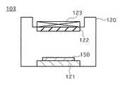
従来のバリア膜形成方法を説明すると、一般的には図15に示すようなスパッタリング装置103が用いられており、真空槽120内に製膜対象である基板150を搬入し、底壁上の基板ホルダー121に載置し、真空槽120内部を真空排気した後、スパッタリングガスと窒素ガスを導入し、スパッタリングガスプラズマを発生させ、基板150に対向配置されたターゲット122をスパッタリングし、ターゲット122から飛び出した金属粒子、又は金属窒化物粒子を基板150表面に付着させ、基板150表面に高融点金属の窒化物薄膜を形成し、その薄膜によってバリア膜を構成させている。
【0006】
このようなスパッタリング装置103では、ターゲット122の裏面に磁石123を配置しておくと、ターゲット122表面のプラズマ密度が高くなり、非常に高い成膜レートでバリア膜を形成できことから、現在では、バリア膜製造方法の主流になっている。
【0007】
しかしながら、スパッタリング法によって形成されたバリア膜ではステップカバレージが悪いという問題がある。特に、図16(a)に示すような、基板151表面のシリコン熱酸化膜152に、高アスペクト比のコンタクトホール160が形成されている場合には、スパッタリング法によってバリア膜を形成すると、同図(b)に示すように、シリコン熱酸化膜152表面に形成されたバリア膜153の膜厚aは厚く、コンタクトホール160底面下に形成されたバリア膜153の膜厚bは薄くなる傾向にあり、基板151面内で、特に膜厚bが薄いコンタクトホール160内では、バリア性が得られなくなってしまうという問題がある。
【0008】
また、コンタクトホール160とターゲット122との相対的な位置関係により、コンタクトホール160の底面の周辺付近では、バリア膜153の膜厚の厚い部分m(ターゲット122に遠い側)と薄い部分n(ターゲット122に近い側)とが発生してしまい、同図(c)に示すように、その表面にAl薄膜154を形成し、熱処理を行った場合には、バリア膜153の膜厚が薄い部分nから基板151内にアルミニウム原子が侵入し、スパイクpが形成され、接続不良を発生させてしまうという問題がある。
【0009】
【発明が解決しようとする課題】
本発明は上記従来技術の不都合を解決するために創作されたものであり、その目的は、バリア性の優れたバリア膜を形成できる技術を提供することにある。
また、ステップカバレージのよい窒化金属薄膜を形成できる技術を提供することにある。
【0010】
【課題を解決するための手段】
上記課題を解決するために、請求項1記載の発明は、基板を真空槽内に搬入し、所定温度まで昇温させた後、含窒素ガスと含高融点金属ガスとを導入し、前記基板上に高融点金属の窒化物薄膜を形成させるバリア膜形成方法であって、前記含窒素ガスと前記含高融点金属ガスのうち、一方のガスを導入し、該一方のガスを真空排気した後、他方のガスを導入して前記基板表面に前記高融点金属の窒化物薄膜を形成し、該他方のガスを真空排気する工程を複数回繰り返すバリア膜形成方法であって、前記高融点金属の窒化物薄膜を形成する際、前記一方のガスを導入して前記真空槽内の圧力を上昇させた後、真空排気して圧力を低下させ、圧力が低下した状態で前記他方のガスを導入して前記真空槽内部の圧力を上昇させ、次いで、前記他方のガスを真空排気した後、前記一方のガスを導入する前に、パージガスを導入して該パージガスを真空排気することを特徴とする。
請求項2記載の発明は、請求項1記載のバリア膜形成方法であって、前記高融点金属の窒化物薄膜を形成する前に、前記含高融点金属ガスの導入と真空排気とを行い、前記高融点金属の窒化物薄膜と基板との界面に、高融点金属薄膜を形成しておくことを特徴とする。
請求項3記載の発明は、請求項1又は請求項2のいずれか1項記載のバリア膜形成方法であって、前記高融点金属の窒化物薄膜を形成した後、前記含高融点金属ガスの導入と真空排気を行い、前記高融点金属の窒化物薄膜表面に高融点金属薄膜を形成することを特徴とする。
請求項4記載の発明は、請求項3記載のバリア膜形成方法であって、前記含高融点金属ガスを導入する際に、還元性ガスを一緒に導入することを特徴とする。
請求項5記載の発明は、請求項1乃至請求項4のいずれか1項記載のバリア膜形成方法であって、前記含高融点金属ガスとして、分子中に、Ti、Ta、Wのいずれか一種の高融点金属を含むガスを用いることを特徴とする。
請求項6記載の発明は、請求項1乃至請求項5のいずれか1項記載のバリア膜形成方法であって、前記含高融点金属ガスとして、分子中にTiを含むガスを使用し、基板温度を200℃以上800℃以下の温度に維持することを特徴とする。
請求項7記載の発明は、請求項1乃至請求項5のいずれか1項記載のバリア膜形成方法であって、前記含高融点金属ガスとして、分子中にWを含むガスを使用し、基板温度を200℃以上800℃以下の温度に維持することを特徴とする。
請求項8記載の発明は、請求項7記載のバリア膜形成方法であって、前記含高融点金属ガスとして、フッ化物ガス、塩化物ガス、臭化物ガス、ヨウ化物ガス、アルコキシドガス、又は有機物ガスのいずれか一種、又は二種以上のガスを用いることを特徴とする。
請求項9記載の発明は、請求項1乃至請求項8のいずれか1項記載のバリア膜形成方法であって、前記含窒素ガスとして、N2ガス、N2H4ガス、NH3ガス、N2Oガスのいずれか一種、又は二種以上のガスを用いることを特徴とする。
【0011】
本発明では、基板を真空槽内に搬入し、所定温度まで昇温させた後、含窒素ガスと含高融点金属ガスとを導入し、前記基板上に高融点金属の窒化物薄膜を形成させるバリア膜形成方法であって、前記含窒素ガスと前記含高融点金属ガスのうち、一方のガスを導入し、該一方のガスを真空排気した後、他方のガスを導入し、該他方のガスを真空排気する工程を複数回繰り返すことができる。
また、本発明では、含窒素ガスと含高融点金属ガスのうち、一方のガスを導入し真空排気すると、基板表面に、そのガスが吸着した状態になり、その状態で他方のガスを導入しているので、吸着ガスによって含窒素ガスと含高融点金属ガスとが基板表面でCVD反応する。
【0012】
吸着されたガス量は、絶縁性薄膜表面、コンタクトホールの壁面、基板表面で同程度なので、基板に設けられたコンタクトホール内に、高融点金属の窒化物薄膜がコンフォーマルに成長し、ステップカバレージのよいバリア膜を得ることができる。
【0013】
CVD反応は、吸着された一方のガスが消費されると停止するが、吸着ガス量は、基板温度を適度に保つことにより、一分子層程度に制御することが可能なので、一回の工程ではCVD反応は僅かしか進行せず、高融点金属の窒化物薄膜が一分子層又は数分子層ずつ積層されるので、ストイキオメトリなバリア膜を得ることができる。
【0014】
この場合、他方のガスを導入し、CVD反応が行われた後、一旦真空排気しているので、副生成物ガスや未反応のガスは除去され、不純物の混入が少なく、高純度のバリア膜を得ることが可能になっている。
【0015】
高融点金属の窒化物薄膜を形成する際、他方のガスを真空排気した後、一方のガスを導入する前に、パージガスを導入し、該パージガスを真空排気することができる。
【0016】
CVD反応が行われた後、パージガスの導入と真空排気を行っており、基板表面や真空槽内壁に吸着した副生成物ガスや未反応ガスがパージガスと交換されるので、次回のCVD反応を行う際、基板表面が清浄な状態になり、一層高純度のバリア膜を得ることが可能となる。
【0017】
パージガスには、Arガス、Heガス等の希ガスの他、N2ガス等の不活性ガスや、H2ガス等の還元性ガスを用いることができる。
【0018】
ところで、一般に、CVD反応を行う際、基板温度が高温であったり、低温であったりした場合には、形成されるバリア膜のバリア性が低下する。実験によると、高融点金属の窒化物薄膜を形成する際の基板温度を200℃以上800℃以下の範囲にしておくと、良好なバリア性を有するバリア膜を得られている。
【0019】
高融点金属の窒化物薄膜を形成する前に、含高融点金属ガスの導入と、真空排気とを行い、高融点金属の窒化物薄膜表面と基板表面との界面に高融点金属薄膜を形成しておく場合、基板には高融点金属薄膜が接触するので、Al薄膜を形成する際の熱処理によって、基板と高融点金属とが反応し、コンタクトホールの抵抗値が低下する。
【0020】
高融点金属の窒化物薄膜を形成した後、含高融点金属ガスの導入と真空排気とを行い、高融点金属の窒化物薄膜表面に高融点金属薄膜を形成する場合は、バリア膜表面の濡れ性が向上し、Al薄膜のフローが容易になるので、高アスペクト比のコンタクトホールでも、底部までAl薄膜で充填することが可能となる。
【0021】
また、高融点金属の窒化物薄膜を形成した後、含高融点金属ガスと同ガスを還元するガス(H2ガス、SiH4ガス等)とを導入し、高融点金属の窒化物薄膜表面に高融点金属を析出させ、コンタクトホールを埋め込んだり、ホール外部の配線を形成したりする、いわゆるブランケットCVD法を行うこともできる。
【0022】
本発明では、分子中に、Ti、Ta、Wのいずれか一種の高融点金属を含むガスを用いることができる。
【0023】
また、そのTi、Ta、Wのいずれか一種の高融点金属を含むガスには、フッ化物ガス、塩化物ガス、臭化物ガス、ヨウ化物ガス、アルコキシドガス、又は有機物ガスのいずれか一種、又は二種以上のガスを用いることができる。
【0024】
他方、含窒素ガスとしては、N2ガス、N2H4ガス、NH3ガス、N2Oガスのいずれか一種のガス、又は二種以上のガスを混合したガスを用いることができる。
【0025】
【発明の実施の形態】
図1を参照し、符号3は、本発明のバリア膜形成方法に用いることができるCVD装置の一例であり、搬送室10を中心として、前処理室11、Al薄膜形成室12、プロセス室(真空槽)20が配置されている。
【0026】
プロセス室20の底壁上にはホットプレート21が設けられており、そのホットプレート21上に基板を配置し、ホットプレート21に通電すると、基板を所望温度に加熱できるように構成されている。
【0027】
また、プロセス室20には、真空排気系26とガス導入系22が接続されており、真空排気系26に設けられた高真空用ポンプを動作させるとプロセス室20内を高真空状態にでき、排気を停止した状態でガス導入系22を用いると、プロセス室20内に、所望種類のガスを圧力制御した状態で導入できるように構成されている。
【0028】
プロセス室20には、リザーバタンク25が設けられており、該リザーバタンク25には、真空排気系26に設けられた低真空用ポンプが接続され、比較的高い圧力状態から、内部を所定圧力以下まで真空排気できるように構成されている。
【0029】
また、リザーバタンク25内部は、プロセス室20の内部と接続できるように構成されており、プロセス室20が比較的高い圧力状態にある場合、接続した状態で低真空用ポンプ25を動作させると、リザーバタンク25の内部を介して、プロセス室20内を所定圧力以下まで真空排気できるように構成されている。
【0030】
本発明のバリア膜形成方法を説明する。
搬送室10内には、基板搬送ロボット15が設けられており、先ず、成膜対象の基板を図示しない基板搬出入室に装着し、基板搬送ロボット15によって前処理室11内に搬送した。
【0031】
該前処理室11内で、基板表面にアルゴンガスプラズマを照射してクリーニングを行い、赤外線ランプによってベーキングし、表面を清浄な状態にした後、搬送室10を通して大気に曝さずに移動させ、プロセス室20内に搬入した(基板ローディング)。
【0032】
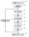
本発明方法の第一例を、図2のフローチャートを用いて説明する。
基板ローディングを行った後(ステップS1)、図1に示すように、プロセス室20内に搬入した基板5を、300℃に温調されているホットプレート21上に載置し、温調した。真空排気系26によってプロセス室20内は真空排気されている(ステップS2)。
【0033】
基板5が300℃に達したとき、プロセス室20内の圧力は2×10⁻⁵Torrになっており、基板5を300℃に維持した状態で真空排気を止めるとともに、ガス導入系22によってNH3ガス(含窒素ガス)を導入し、プロセス室20内を圧力3×10⁻¹TorrのNH3ガスで充満させた。
【0034】
その状態を2秒間維持し、NH3ガスを基板5表面に吸着させた後(ステップS3)、予め真空状態にしておいたリザーバタンク25をプロセス室20に接続し、プロセス室20内の圧力を急速に低下させると共に、真空排気系26の低真空用ポンプによって、リザーバタンク25を介してプロセス室20内を真空排気した。
【0035】
プロセス室20内が所定圧力まで低下したところで、リザーバタンク25を切り離し、真空排気系26の高真空用ポンプによってプロセス室20内を直接真空排気したところ、プロセス室20内の圧力は、3×10⁻¹Torrの圧力から約10秒で5×10⁻⁵Torrまで低下した(ステップS4)。
【0036】
その圧力下で、ガス導入系22によってTiCl4ガス(含高融点金属ガス)を導入し、プロセス室20内を圧力5×10⁻¹TorrのTiCl4ガスで充満させた。
【0037】
その状態を2秒間維持し、基板5表面に吸着されたNH3ガスとTiCl4ガスとを反応させ、基板5表面にTiN薄膜(高融点金属の窒化物薄膜)を形成した後(ステップS5)、上記ステップS4と同様に真空排気を行い、副生成物ガスや未反応ガスを排気した(ステップS6)。
【0038】
その後、ガス導入系22によってArガス(パージガス)を導入し、プロセス室20内を圧力5×10⁻¹TorrのArガスで充満させ、2秒間その状態を維持し(ステップS7)、基板5表面やプロセス室20の壁面に吸着されていた未反応ガスや副生成物ガスをArガスに交換させ、その後、上記ステップS4と同様に排気した(ステップS8)。
【0039】
Arガスの排気後、再びNH3ガス導入工程に戻り(ステップS9)、上記NH3ガスの導入からArガスの排気(ステップS3〜S8)までの処理を、合計50回繰り返し行った。
【0040】
最後のArガスの排気を行った後(ステップS8)、基板5をプロセス室20から搬出し(ステップS10)、図示しない基板搬出入室からCVD装置3の外部に取り出した。
【0041】
基板5の断面をSEMを用いて観察した結果を図7に模式的に示す。この基板5は、シリコン基板51と、該シリコン基板51表面に形成されたシリコン熱酸化膜52とを有しており、シリコン熱酸化膜52には底面にシリコン基板51が露出したコンタクトホール60が設けられている。
【0042】
観察結果によると、シリコン熱酸化膜52表面と、コンタクトホール60底面にTiN薄膜がバリア膜53として形成されており、シリコン熱酸化膜52表面の膜厚a、コンタクトホール60底面の膜厚bは、共に200Åであり、ステップカバレージ性は良好であった。
また、コンタクトホール60の壁面にも、膜厚cが200ÅのTiN薄膜が形成されており、バリア膜53はコンフォーマルに成長していることが確認された。
【0043】
オージェ電子分光分析装置を用いてバリア膜53の組成分析を行ったところ、TiNx,x=0.9〜1.1 であり、ほぼ、ストイキオメトリな薄膜であることが確認された。分析結果では、Cl等の不純物は検出されなかった。
【0044】
次に、膜厚1.0μmのシリコン熱酸化膜に、直径が0.5μm又は0.7μmのコンタクトホールが多数形成された基板を用い、繰り返し回数を20回として上記図2のフローチャートと同じ手順でTiN薄膜から成るバリア膜を形成した。
【0045】
バリア膜の形成後、搬送室10を通し、大気に曝さない状態で低温Al薄膜形成室12に搬入し、ロングスロースパッタリング(LTS)法により、1層目の低温Al薄膜を形成した後、高温Al薄膜形成室13にて2層目のAl薄膜を450℃でフローさせながら形成した(いわゆる2ステップフロー法)後、約10秒で100℃以下に冷却して取り出した。
【0046】
その基板の断面を観察した結果を、図8に模式的に示す。シリコン熱酸化膜52表面、及びコンタクトホール60'の底面上には、膜厚70ÅのTiN薄膜がコンフォーマルに形成されており、ステップカバレージのよいバリア膜53'が得られた。
【0047】
バリア膜53'表面に形成した二層のAl−Cu合金薄膜541、542は、合計8000Åの膜厚であり、0.7μmのコンタクトホール60'内ではAl薄膜が底部まで充填されていた。0.5μmのコンタクトホール60'の場合、一部のものにボイドが観察された。0.5μmのコンタクトホールの場合、後述する本発明の第三例のバリア膜形成方法を用いる必要があることが分かった。
なお、シリコン基板51には、アルミニウムの拡散によるスパイクは観察されておらず、バリア膜53'のバリア性が優れていることが確認された。
【0048】
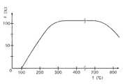
次に、バリア膜形成中の基板温度とバリア性の関係を図11に示す。基板温度を変えた以外の他の条件は上記実施例と同じである。図11の横軸Tは基板温度であり、縦軸F(%)は、
F=スパイクの無いコンタクトホール数/コンタクトホール総個数
である。
【0049】
基板温度が200℃未満の場合、又は800℃を超えた場合は、得られたバリア膜のFの値が低下しており、TiN薄膜から成るバリア膜を形成する場合は、300℃以上800℃以下の温度範囲が適していることが分かる。
【0050】
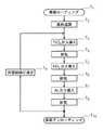
なお、上記第一例では、NH3ガスを導入した後、TiCl4ガスを導入したが、図3のフローチャートに示すように、NH3ガスとTiCl4ガスの導入順序を交換してもよい。
【0051】
図3のフローチャートを説明すると、基板のローディングと温調を行った後(ステップT1、T2)、最初にTiCl4ガスの導入と真空排気を行い(ステップT3、T4)、先ず、基板表面にTiCl4ガスを吸着させており、その状態でNH3ガスを導入し(ステップT5)、CVD反応を行わせて基板表面にTiNを堆積させ、次いで、真空排気を行い(ステップT6)、副生成物ガスや未反応ガスを排気した後、パージガスとしてArガスを導入し(ステップT7)、吸着ガスをパージガスと交換させている。
【0052】
パージガスの真空排気を行った後(ステップT8)、TiCl4の導入工程に戻り(ステップT9)、これらTiCl4の導入からArガスの排気までの工程を所望回数繰り返し行った後、基板のアンローディングを行うと(ステップT10)、図2のフローチャートに示した工程と同様に、基板表面にTiN薄膜から成るバリア膜を形成することができる。
【0053】
この図3のフローチャートによって基板表面にバリア膜を形成した後、断面を観察したところ、上記図7に示したものと同様に、バリア膜はコンタクトホール内にコンフォーマルに成長しており、ステップカバレージ性は良好であった。
【0054】
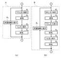
次に、本発明の第二例の工程を説明する。図4は、その第二例の工程の一部を示したものであり、同図(a)はTi薄膜を形成する工程A、同図(b)はTiN薄膜を形成する工程Bである。
【0055】
工程Aを説明すると、ホットプレート21上に基板を配置し、真空排気した状態で、TiCl4ガスの導入と真空排気を行った後(ステップA1、A2)、還元性のパージガスであるH2ガスの導入と真空排気を行い(ステップA3、A4)、TiCl4ガスを導入する工程に戻る(ステップA5)。TiCl4ガスの導入からH2ガスの真空排気(ステップA1〜A4)を所望回数繰り返すと、基板上にTi薄膜を形成することができる。
【0056】
工程Bを説明すると、NH4ガスの導入と真空排気(ステップB1、B2)、TiCl4ガスの導入と真空排気(ステップB3、B4)、Arガスの導入と真空排気(ステップB5、B6)を順次行い、NH4ガスの導入工程に戻る(ステップB7)。NH4ガスの導入からH2ガスの真空排気までの工程(ステップB1〜B6)を所望回数繰り返すと、基板上にTiN薄膜を形成することができる。
【0057】
上記図4(a)、(b)に示した工程を用い、図5のフローチャートに示すように、基板ローディングと300℃の温調を行った後(ステップU1、U2)、工程A(繰り返し回数5回)、工程B(繰り返し回数15回)を行い、Ti薄膜とTiN膜をこの順で形成し(ステップU3、U4)、アンローディングした(ステップU5)。
この第二例では、図9に示すように、Ti薄膜55と、該Ti薄膜55表面に形成されたTiN薄膜56とでバリア膜63が構成された。
【0058】
そのバリア膜63表面に、2ステップフロー法によってAl薄膜を形成したところ、0.7μmのコンタクトホール61内を底部まで充填することができた。このバリア膜63のバリア性は第一例の場合と同等であった。
【0059】
Al薄膜で充填された第一例のコンタクトホール60と第二例のコンタクトホール61の抵抗値を比較したところ、第二例の場合は、バリア膜63のTi薄膜55がシリコン基板51と接しているため、Al薄膜を形成する際の熱処理の影響により、シリコン基板51とTi薄膜55の界面がシリサイド化しており、第一例のコンタクトホール60に比べると、第二例のコンタクトホール61の抵抗値は低かった。
【0060】
なお、この第二例において、基板を昇温させた後、TiCl4ガスを導入する前に、NH3ガスを導入し、真空排気した後、Arガスの導入と真空排気を行う前処理工程を設け、1回又は2回の前処理工程を行っておくと、ステップカバレージ性、組成、バリア性を第一例の場合と同等にしたまま、エンクローチメントの発生を抑制できることが確認された。
【0061】
次に、本発明の第三例の工程を図6に示して説明する。
基板ローディングと基板の300℃への昇温後(ステップV1、V2)、工程A、工程B、工程Aを行い(ステップV3、V4、V5)、基板のアンローディングを行った(ステップV6)。工程Aの繰り返し回数は5回、工程Bの繰り返し回数は15回である。
【0062】
この場合、図10に模式的に示すように、Ti薄膜57、TiN薄膜58、Ti薄膜59がこの順で形成されたバリア膜73が得られた。
このバリア膜73表面に2ステップフロー法によってAl薄膜を形成したところ、Al薄膜が濡れ性のよいTi薄膜59表面に形成されたため、0.5μmのコンタクトホール62の底部までAl薄膜によって完全に充填することができた。バリア膜73の成長量、ステップカバレージ性、組成、バリア性は、第一例、第二例のバリア膜53、53'、63と同等であった。
【0063】
なお、上記実施例では、高融点金属にTiを用いた場合を説明したが、WやTaを分子中に含むガスを用いることができる。また、NH3ガスを含窒素ガスとして用いたが、NH3ガスに換え、N2ガス、NH4ガスやN2Oガスを用いることができる。また、NH3ガス、N2ガス、NH4ガス、N2Oガスを二種以上混合して用いることもできる。
【0064】
更に、上記実施例では高融点金属の塩化物ガスを用いたが、Ti、W、又はTaのフッ化物ガス、塩化物ガス、臭化物ガス、ヨウ化物ガス、アルコキシドガス、又はTDMAT(Ti[N(CH3)2]4:テトラキスジメチルアミノチタン)や、TDEAT(Ti[N(C2H5)2]4:テトラキスジエチルアミノチタン等の有機金属化合物ガスを用いることができる。また、Arパージ工程は省略してもほぼ同等の膜が得られる。
【0065】
タングステンのフッ化物ガスを用いた場合の工程を本発明の第四例として図12のフローチャートを参照して説明する。
先ず、プロセス室20内への基板ローディングを行い(ステップW1)、300℃に温調したホットプレート21上に載置し、基板を温調した(ステップW2)。
【0066】
ガス導入系によってプロセス室20内にNH3ガスを導入し、2×10⁻¹Torrの圧力で2秒間充満させた(ステップW3)。次いで、真空排気し(ステップW4)、プロセス室20内を10秒間で5×10⁻³Torrの圧力まで低下させた。このときはリザーバタンク25は使用しなかった。
【0067】
その状態からプロセス室20内にWF6ガスを導入し、2×10⁻¹Torrの圧力で2秒間充満させ(ステップW5)た後、同様に真空排気し、5×10⁻³Torrの圧力まで10秒間で低下させた。
アルゴンガスの導入は行わず、NH3ガスの導入からWF6ガスの排気までの工程(ステップW3〜W6)を50回繰り返して行った(ステップW9)。
【0068】
基板アンローディング(ステップW10)後、基板の断面をSEMを用いて観察した。その結果を図13の符号15で模式的に示す。形成されたバリア膜(WN薄膜)83の膜厚は、基板表面、コンタクトホール底面、コンタクトホール側面(符号a〜c)ともに200Åであり、コンフォーマルに成長しており、良好なステップカバレージが得られた。
オージェ電子分光分析装置を用い、得られたバリア膜83の組成分析を行ったところ、WNx,x=0.4〜0.6 であった。
【0069】
そのバリア膜83表面に、第一例の場合と同様に、2ステップフロー法にてAl薄膜を形成したところ、図8に示した場合と同様に、コンタクトホール内は1層目の低温Al薄膜と2層目の高温Al薄膜とで充填された。この場合も、シリコン基板中にはアルミニウムの拡散によるスパイクは観察されなかった。
【0070】
このバリア膜83についても、基板温度を変えて形成し、バリア性との関係を調べた。その結果を図14のグラフに示す。横軸Tは基板温度、縦軸Fは、上記と同様に、
F=スパイクの無いコンタクトホール数/コンタクトホール総個数
である。
【0071】
この図14のグラフからは、基板温度200℃未満、又は700℃を超える温度では、得られたバリア膜83のF値が低下している。従って、WN薄膜から成るバリア膜83の場合、250℃以上、600℃以下の温度範囲が適していることが分かる。
【0072】
なお、上記第一例〜第四例の工程については、バリア膜形成後、プラズマ処理を行う工程を追加し、バリア膜とその表面に形成する金属薄膜との間の比抵抗を下げるようにしてもよい。
【0073】
【発明の効果】
ステップカバレージ性、バリア性の優れたバリア膜を得ることができる。
組成がストイキオメトリで高純度のバリア膜を得ることができる。
【図面の簡単な説明】
【図1】本発明に用いることができるCVD装置の一例
【図2】本発明の第一例の工程を説明するためのフローチャート
【図3】第一例を変形した工程を説明するためのフローチャート
【図4】(a):第二例のTi薄膜形成工程を説明するためのフローチャート
(b):第二例のTiN薄膜形成工程を説明するためのフローチャート
【図5】本発明の第二例の工程を説明するためのフローチャート
【図6】本発明の第三例の工程を説明するためのフローチャート
【図7】第一例で得られたバリア膜の断面を説明するための図
【図8】その表面にAl薄膜を形成した状態の断面図
【図9】第二例で得られたバリア膜の断面を説明するための図
【図10】第三例で得られたバリア膜の断面を説明するための図
【図11】TiN薄膜を形成する際の基板温度とバリア性の関係を説明するためのグラフ
【図12】本発明の第四例の工程を説明するためのフローチャート
【図13】第四例で得られたバリア膜の断面を説明するための図
【図14】WN薄膜を形成する際の基板温度とバリア性の関係を説明するためのグラフ
【図15】従来技術のバリア膜形成方法に用いられていたスパッタリング装置
【図16】(a)〜(c):従来技術のバリア膜の特性を説明するための図
【符号の説明】
5、5'、15……基板 20……真空槽 53、63、73、83……バリア膜 53、56、58、83……高融点金属の窒化物薄膜 55、57、59……高融点金属薄膜
Claims (9)
- 基板を真空槽内に搬入し、所定温度まで昇温させた後、含窒素ガスと含高融点金属ガスとを導入し、
前記基板上に高融点金属の窒化物薄膜を形成させるバリア膜形成方法であって、
前記含窒素ガスと前記含高融点金属ガスのうち、一方のガスを導入し、該一方のガスを真空排気した後、他方のガスを導入して前記基板表面に前記高融点金属の窒化物薄膜を形成し、該他方のガスを真空排気する工程を複数回繰り返すバリア膜形成方法であって、
前記高融点金属の窒化物薄膜を形成する際、前記一方のガスを導入して前記真空槽内の圧力を上昇させた後、真空排気して圧力を低下させ、圧力が低下した状態で前記他方のガスを導入して前記真空槽内部の圧力を上昇させ、次いで、前記他方のガスを真空排気した後、前記一方のガスを導入する前に、パージガスを導入して該パージガスを真空排気することを特徴とするバリア膜形成方法。 - 請求項1記載のバリア膜形成方法であって、前記高融点金属の窒化物薄膜を形成する前に、前記含高融点金属ガスの導入と真空排気とを行い、前記高融点金属の窒化物薄膜と基板との界面に、高融点金属薄膜を形成しておくことを特徴とするバリア膜形成方法。
- 前記高融点金属の窒化物薄膜を形成した後、前記含高融点金属ガスの導入と真空排気を行い、前記高融点金属の窒化物薄膜表面に高融点金属薄膜を形成することを特徴とする請求項1又は請求項2のいずれか1項記載のバリア膜形成方法。
- 前記含高融点金属ガスを導入する際に、還元性ガスを一緒に導入することを特徴とする請求項3記載のバリア膜形成方法。
- 前記含高融点金属ガスとして、分子中に、Ti、Ta、Wのいずれか一種の高融点金属を含むガスを用いることを特徴とする請求項1乃至請求項4のいずれか1項記載のバリア膜形成方法。
- 前記含高融点金属ガスとして、分子中にTiを含むガスを使用し、基板温度を200℃以上800℃以下の温度に維持することを特徴とする請求項1乃至請求項5のいずれか1項記載のバリア膜形成方法。
- 前記含高融点金属ガスとして、分子中にWを含むガスを使用し、基板温度を200℃以上800℃以下の温度に維持することを特徴とする請求項1乃至請求項5のいずれか1項記載のバリア膜形成方法。
- 前記含高融点金属ガスとして、フッ化物ガス、塩化物ガス、臭化物ガス、ヨウ化物ガス、アルコキシドガス、又は有機物ガスのいずれか一種、又は二種以上のガスを用いることを特徴とする請求項7記載のバリア膜形成方法。
- 前記含窒素ガスとして、N2ガス、N2H4ガス、NH3ガス、N2Oガスのいずれか一種、又は二種以上のガスを用いることを特徴とする請求項1乃至請求項8のいずれか1項記載のバリア膜形成方法。
Priority Applications (1)
| Application Number | Priority Date | Filing Date | Title |
|---|---|---|---|
| JP22571197AJP4097747B2 (ja) | 1997-08-07 | 1997-08-07 | バリア膜形成方法 |
Applications Claiming Priority (1)
| Application Number | Priority Date | Filing Date | Title |
|---|---|---|---|
| JP22571197AJP4097747B2 (ja) | 1997-08-07 | 1997-08-07 | バリア膜形成方法 |
Related Child Applications (2)
| Application Number | Title | Priority Date | Filing Date |
|---|---|---|---|
| JP2005290086ADivisionJP4098326B2 (ja) | 2005-10-03 | 2005-10-03 | バリア膜形成方法 |
| JP2007286311ADivisionJP4786629B2 (ja) | 2007-11-02 | 2007-11-02 | バリア膜形成方法 |
Publications (2)
| Publication Number | Publication Date |
|---|---|
| JPH1154459A JPH1154459A (ja) | 1999-02-26 |
| JP4097747B2true JP4097747B2 (ja) | 2008-06-11 |
Family
ID=16833615
Family Applications (1)
| Application Number | Title | Priority Date | Filing Date |
|---|---|---|---|
| JP22571197AExpired - Fee RelatedJP4097747B2 (ja) | 1997-08-07 | 1997-08-07 | バリア膜形成方法 |
Country Status (1)
| Country | Link |
|---|---|
| JP (1) | JP4097747B2 (ja) |
Families Citing this family (32)
| Publication number | Priority date | Publication date | Assignee | Title |
|---|---|---|---|---|
| US6410433B1 (en)* | 1999-04-27 | 2002-06-25 | Tokyo Electron Limited | Thermal CVD of TaN films from tantalum halide precursors |
| US6265311B1 (en)* | 1999-04-27 | 2001-07-24 | Tokyo Electron Limited | PECVD of TaN films from tantalum halide precursors |
| US6413860B1 (en)* | 1999-04-27 | 2002-07-02 | Tokyo Electron Limited | PECVD of Ta films from tanatalum halide precursors |
| US6410432B1 (en)* | 1999-04-27 | 2002-06-25 | Tokyo Electron Limited | CVD of integrated Ta and TaNx films from tantalum halide precursors |
| US6268288B1 (en)* | 1999-04-27 | 2001-07-31 | Tokyo Electron Limited | Plasma treated thermal CVD of TaN films from tantalum halide precursors |
| US6391785B1 (en)* | 1999-08-24 | 2002-05-21 | Interuniversitair Microelektronica Centrum (Imec) | Method for bottomless deposition of barrier layers in integrated circuit metallization schemes |
| JP4746234B2 (ja)* | 1999-10-15 | 2011-08-10 | エーエスエム インターナショナル エヌ.ヴェー. | 感受性表面上にナノラミネート薄膜を堆積するための方法 |
| US6482733B2 (en)* | 2000-05-15 | 2002-11-19 | Asm Microchemistry Oy | Protective layers prior to alternating layer deposition |
| US7101795B1 (en)* | 2000-06-28 | 2006-09-05 | Applied Materials, Inc. | Method and apparatus for depositing refractory metal layers employing sequential deposition techniques to form a nucleation layer |
| US7964505B2 (en) | 2005-01-19 | 2011-06-21 | Applied Materials, Inc. | Atomic layer deposition of tungsten materials |
| CN100446218C (zh)* | 2000-11-17 | 2008-12-24 | 东京毅力科创株式会社 | 金属膜的形成方法和钨膜的形成方法 |
| AU2002221122A1 (en) | 2000-12-12 | 2002-06-24 | Tokyo Electron Limited | Thin film forming method and thin film forming device |
| US6951804B2 (en) | 2001-02-02 | 2005-10-04 | Applied Materials, Inc. | Formation of a tantalum-nitride layer |
| US6849545B2 (en)* | 2001-06-20 | 2005-02-01 | Applied Materials, Inc. | System and method to form a composite film stack utilizing sequential deposition techniques |
| TW581822B (en)* | 2001-07-16 | 2004-04-01 | Applied Materials Inc | Formation of composite tungsten films |
| TW589684B (en)* | 2001-10-10 | 2004-06-01 | Applied Materials Inc | Method for depositing refractory metal layers employing sequential deposition techniques |
| WO2003038892A2 (en)* | 2001-10-26 | 2003-05-08 | Applied Materials, Inc. | Atomic-layer-deposited tantalum nitride and alpha-phase tantalum as barrier layers for copper metallization |
| EP1420080A3 (en)* | 2002-11-14 | 2005-11-09 | Applied Materials, Inc. | Apparatus and method for hybrid chemical deposition processes |
| JP4429919B2 (ja) | 2002-12-27 | 2010-03-10 | 株式会社アルバック | 窒化タングステン膜の成膜方法 |
| WO2004112114A1 (ja)* | 2003-06-16 | 2004-12-23 | Tokyo Electron Limited | 成膜方法、半導体装置の製造方法、半導体装置および成膜装置 |
| KR101178743B1 (ko) | 2004-04-12 | 2012-09-07 | 가부시키가이샤 알박 | 배리어막의 형성 방법, 및 전극막의 형성 방법 |
| JP2006176823A (ja)* | 2004-12-22 | 2006-07-06 | Ulvac Japan Ltd | 成膜装置 |
| JP4931171B2 (ja) | 2005-03-03 | 2012-05-16 | 株式会社アルバック | タンタル窒化物膜の形成方法 |
| JP4931170B2 (ja) | 2005-03-03 | 2012-05-16 | 株式会社アルバック | タンタル窒化物膜の形成方法 |
| JP4783585B2 (ja)* | 2005-05-02 | 2011-09-28 | 株式会社アルバック | 成膜装置 |
| JP4734020B2 (ja)* | 2005-05-02 | 2011-07-27 | 株式会社アルバック | 成膜装置 |
| US7273811B2 (en)* | 2005-06-27 | 2007-09-25 | The Regents Of The University Of California | Method for chemical vapor deposition in high aspect ratio spaces |
| WO2007066472A1 (ja) | 2005-12-06 | 2007-06-14 | Ulvac, Inc. | ガスヘッド及び薄膜製造装置 |
| JP2008192835A (ja)* | 2007-02-05 | 2008-08-21 | Tokyo Electron Ltd | 成膜方法,基板処理装置,および半導体装置 |
| KR101275025B1 (ko)* | 2007-07-12 | 2013-06-14 | 삼성전자주식회사 | 반도체 소자용 배선 구조물 및 이의 형성방법 |
| JP5581642B2 (ja)* | 2009-10-05 | 2014-09-03 | 住友電気工業株式会社 | 半導体装置の製造方法 |
| JP4943536B2 (ja)* | 2009-10-30 | 2012-05-30 | 株式会社日立国際電気 | 半導体装置の製造方法、基板処理方法及び基板処理装置 |
- 1997
- 1997-08-07JPJP22571197Apatent/JP4097747B2/janot_activeExpired - Fee Related
Also Published As
| Publication number | Publication date |
|---|---|
| JPH1154459A (ja) | 1999-02-26 |
Similar Documents
| Publication | Publication Date | Title |
|---|---|---|
| JP4097747B2 (ja) | バリア膜形成方法 | |
| KR100236668B1 (ko) | 저항 및 결함밀도가 낮은 텅스텐 접점을 실리콘 반도체 웨이퍼에 형성하기위한 방법 | |
| US6602770B2 (en) | Silicon layer to improve plug filling by CVD | |
| US6464779B1 (en) | Copper atomic layer chemical vapor desposition | |
| US7211144B2 (en) | Pulsed nucleation deposition of tungsten layers | |
| US6399490B1 (en) | Highly conformal titanium nitride deposition process for high aspect ratio structures | |
| US7419904B2 (en) | Method for forming barrier film and method for forming electrode film | |
| US6475912B1 (en) | Semiconductor device and method and apparatus for fabricating the same while minimizing operating failures and optimizing yield | |
| JP2017069313A (ja) | 半導体装置の製造方法、基板処理装置、ガス供給システムおよびプログラム | |
| US20040235191A1 (en) | Film forming method | |
| EP0566040A2 (en) | Process for selectively depositing copper aluminum alloy onto a substrate | |
| JP2009010434A (ja) | 低温で基板のステップカバレージを改良する方法及び装置 | |
| JP2004536960A (ja) | フッ素を含まないタングステン核生成によるw−cvd | |
| JP2002334884A (ja) | 半導体素子の金属配線形成方法 | |
| KR102017944B1 (ko) | 니켈 배선의 제조 방법 | |
| JP3971192B2 (ja) | Cvd装置 | |
| JP4786629B2 (ja) | バリア膜形成方法 | |
| US8034403B2 (en) | Method for forming copper distributing wires | |
| JP4098326B2 (ja) | バリア膜形成方法 | |
| JP2006066642A (ja) | 半導体装置の製造方法 | |
| JP4931170B2 (ja) | タンタル窒化物膜の形成方法 | |
| JP3718297B2 (ja) | 薄膜作製方法および薄膜作製装置 | |
| JP4931171B2 (ja) | タンタル窒化物膜の形成方法 | |
| JP3281816B2 (ja) | 銅配線製造方法 | |
| JP3938450B2 (ja) | バリア膜製造方法 |
Legal Events
| Date | Code | Title | Description |
|---|---|---|---|
| A621 | Written request for application examination | Free format text:JAPANESE INTERMEDIATE CODE: A621 Effective date:20040401 | |
| A977 | Report on retrieval | Free format text:JAPANESE INTERMEDIATE CODE: A971007 Effective date:20050301 | |
| A131 | Notification of reasons for refusal | Free format text:JAPANESE INTERMEDIATE CODE: A131 Effective date:20070904 | |
| A521 | Written amendment | Free format text:JAPANESE INTERMEDIATE CODE: A821 Effective date:20071105 Free format text:JAPANESE INTERMEDIATE CODE: A523 Effective date:20071105 | |
| A131 | Notification of reasons for refusal | Free format text:JAPANESE INTERMEDIATE CODE: A131 Effective date:20071218 | |
| A521 | Written amendment | Free format text:JAPANESE INTERMEDIATE CODE: A523 Effective date:20080215 Free format text:JAPANESE INTERMEDIATE CODE: A821 Effective date:20080215 | |
| TRDD | Decision of grant or rejection written | ||
| A01 | Written decision to grant a patent or to grant a registration (utility model) | Free format text:JAPANESE INTERMEDIATE CODE: A01 Effective date:20080311 | |
| A61 | First payment of annual fees (during grant procedure) | Free format text:JAPANESE INTERMEDIATE CODE: A61 Effective date:20080312 | |
| R150 | Certificate of patent or registration of utility model | Free format text:JAPANESE INTERMEDIATE CODE: R150 | |
| FPAY | Renewal fee payment (event date is renewal date of database) | Free format text:PAYMENT UNTIL: 20110321 Year of fee payment:3 | |
| FPAY | Renewal fee payment (event date is renewal date of database) | Free format text:PAYMENT UNTIL: 20110321 Year of fee payment:3 | |
| FPAY | Renewal fee payment (event date is renewal date of database) | Free format text:PAYMENT UNTIL: 20140321 Year of fee payment:6 | |
| R250 | Receipt of annual fees | Free format text:JAPANESE INTERMEDIATE CODE: R250 | |
| R250 | Receipt of annual fees | Free format text:JAPANESE INTERMEDIATE CODE: R250 | |
| LAPS | Cancellation because of no payment of annual fees |