JP4097681B1 - connector - Google Patents
connectorDownload PDFInfo
- Publication number
- JP4097681B1 JP4097681B1JP2007023244AJP2007023244AJP4097681B1JP 4097681 B1JP4097681 B1JP 4097681B1JP 2007023244 AJP2007023244 AJP 2007023244AJP 2007023244 AJP2007023244 AJP 2007023244AJP 4097681 B1JP4097681 B1JP 4097681B1
- Authority
- JP
- Japan
- Prior art keywords
- contact
- electric wire
- connector
- housing
- wire
- Prior art date
- Legal status (The legal status is an assumption and is not a legal conclusion. Google has not performed a legal analysis and makes no representation as to the accuracy of the status listed.)
- Expired - Fee Related
Links
- 238000003825pressingMethods0.000claimsdescription6
- 230000004308accommodationEffects0.000abstract3
- 239000004020conductorSubstances0.000description24
- 230000013011matingEffects0.000description13
- 238000003860storageMethods0.000description5
- 239000000758substrateSubstances0.000description5
- 238000002788crimpingMethods0.000description4
- 238000005452bendingMethods0.000description3
- 230000005540biological transmissionEffects0.000description2
- 239000003989dielectric materialSubstances0.000description2
- 238000000034methodMethods0.000description2
- 238000004080punchingMethods0.000description2
- 239000000463materialSubstances0.000description1
- 238000000465mouldingMethods0.000description1
- 239000011347resinSubstances0.000description1
- 229920005989resinPolymers0.000description1
- 238000003466weldingMethods0.000description1
Images


Classifications
- H—ELECTRICITY
- H01—ELECTRIC ELEMENTS
- H01R—ELECTRICALLY-CONDUCTIVE CONNECTIONS; STRUCTURAL ASSOCIATIONS OF A PLURALITY OF MUTUALLY-INSULATED ELECTRICAL CONNECTING ELEMENTS; COUPLING DEVICES; CURRENT COLLECTORS
- H01R9/00—Structural associations of a plurality of mutually-insulated electrical connecting elements, e.g. terminal strips or terminal blocks; Terminals or binding posts mounted upon a base or in a case; Bases therefor
- H01R9/03—Connectors arranged to contact a plurality of the conductors of a multiconductor cable, e.g. tapping connections
- H01R9/05—Connectors arranged to contact a plurality of the conductors of a multiconductor cable, e.g. tapping connections for coaxial cables
- H01R9/053—Connectors arranged to contact a plurality of the conductors of a multiconductor cable, e.g. tapping connections for coaxial cables using contact members penetrating insulation
- H—ELECTRICITY
- H01—ELECTRIC ELEMENTS
- H01R—ELECTRICALLY-CONDUCTIVE CONNECTIONS; STRUCTURAL ASSOCIATIONS OF A PLURALITY OF MUTUALLY-INSULATED ELECTRICAL CONNECTING ELEMENTS; COUPLING DEVICES; CURRENT COLLECTORS
- H01R9/00—Structural associations of a plurality of mutually-insulated electrical connecting elements, e.g. terminal strips or terminal blocks; Terminals or binding posts mounted upon a base or in a case; Bases therefor
- H01R9/03—Connectors arranged to contact a plurality of the conductors of a multiconductor cable, e.g. tapping connections
- H01R9/05—Connectors arranged to contact a plurality of the conductors of a multiconductor cable, e.g. tapping connections for coaxial cables
- H01R9/0518—Connection to outer conductor by crimping or by crimping ferrule
Landscapes
- Coupling Device And Connection With Printed Circuit (AREA)
- Connections By Means Of Piercing Elements, Nuts, Or Screws (AREA)
- Details Of Connecting Devices For Male And Female Coupling (AREA)
- Multi-Conductor Connections (AREA)
Abstract
Translated fromJapaneseDescription
Translated fromJapanese本発明は、電線とコンタクトを接続するコネクタに関する。 The present invention relates to a connector for connecting an electric wire and a contact.
先行技術1には、簡易圧着部に設けられた接触片で同軸ケーブルの外皮を突き破って同軸ケーブルの外部導体編組に接触するようにし、プラグ内部コンタクトで誘電体を切り裂いて中心導体と接触させる同軸プラグコネクタが開示されている(例えば、特許文献1を参照)。 In
先行技術2には、導電基板の両側縁から起立する側壁を設け、側壁の内側に位置する導電基板から起立する複数の角状柱を導電基板の長手方向に千鳥状に配列し、角状柱の先端に斜面を形成し、斜面と角状柱の内壁面の角部に、被覆電線の被覆部に食い込む刃部を形成して端子の結線部を構成した端子の導体接続部構造が開示されている(例えば、特許文献2を参照)。 In Prior Art 2, a side wall standing from both side edges of the conductive substrate is provided, and a plurality of rectangular pillars standing from the conductive substrate located inside the side walls are arranged in a staggered manner in the longitudinal direction of the conductive substrate. A terminal conductor connection structure is disclosed in which a slope is formed at the tip of the wire, and a blade portion that cuts into the sheath portion of the coated electric wire is formed at the corner portion of the slope and the inner wall surface of the rectangular column to constitute the terminal connection portion. (For example, refer to Patent Document 2).
この端子の導体接続部構造では、被覆電線を両側壁の間に挿入したときに、被覆電線の導体部が蛇行上に弾性変形し、弾性力により角状柱に圧接するように角状柱を配置している。 In this conductor connection part structure of the terminal, when the covered electric wire is inserted between the both side walls, the conductor of the covered electric wire is elastically deformed in a meandering manner, and the square column is pressed against the square column by the elastic force. It is arranged.
特許文献1では、簡易圧着部を上部治具と下部治具とによって押圧して、上部治具により簡易圧着部をカールして同軸ケーブルの外皮に食い込ませ、一方、簡易圧着部の接触片を同軸ケーブルの外皮を突き破り、外部導体編組に接触させるので簡易圧着部が変形することがあり、圧接に適した位置へ同軸ケーブルを誘導し難く、同軸ケーブルの位置ずれが生じるという問題がある。 In
特許文献2では、導電基板の側壁が薄いことから、角状柱を被覆電線の被覆部に食い込ませる際に、導電基板の側壁が変形することがあり、被覆電線の導体部と角状柱との接触位置へ誘導できず、接触不良となるという問題がある。 In Patent Document 2, since the side wall of the conductive substrate is thin, the side wall of the conductive substrate may be deformed when the rectangular column is bitten into the coated portion of the covered electric wire. There is a problem that it cannot be guided to the contact position, resulting in poor contact.
それ故に、本発明の課題は、電線とコンタクトを確実にかつ容易に接続することができ、接続信頼性を向上することができるコネクタを提供することにある。 Therefore, the subject of this invention is providing the connector which can connect an electric wire and a contact reliably and easily and can improve connection reliability.
本発明の他の課題は、電線とコンタクトとの接続工程が簡易になり、小型化が可能となり、さらに伝送特性あるいは高周波特性が良好なコネクタを提供することにある。 Another object of the present invention is to provide a connector in which the connection process between the electric wire and the contact is simplified, the size can be reduced, and the transmission characteristic or the high frequency characteristic is good.
本発明は、電線と接続するコネクタにおいて、コンタクトと、該コンタクトを保持するハウジングとを有し、前記コンタクトは、前記電線の芯線と接続する結線部を有し、前記ハウジングは、前記電線を覆いかつ前記結線部に向けて前記電線を押圧し前記芯線と前記結線部とを接続させる覆い部と、前記電線を収容する収容部とを有し、前記結線部は前記収容部に収容され、前記収容部は前記電線を位置決めする位置決め部を有することを特徴とするコネクタであることを最も主要な特徴とする。 The present invention provides a connector for connecting to an electric wire, comprising a contact and a housing for holding the contact, wherein the contact has a connection portion connected to a core wire of the electric wire, and the housing covers the electric wire. And a cover portion that presses the electric wire toward the connection portion to connect the core wire and the connection portion, and a storage portion that stores the electric wire, the connection portion being received in the storage portion, The housing part is a connector characterized by having a positioning part for positioning the electric wire.
本発明のコネクタによれば、ハウジングの覆い部によって電線をハウジングの収容部の位置決め部へ適切に位置させ保持できるので、電線とコンタクトとの接続工程が簡易になり、電線の芯線とコンタクトの結線部とを確実かつ容易に接続することができ、信頼性を向上することができる。 According to the connector of the present invention, since the electric wire can be appropriately positioned and held in the positioning portion of the housing housing portion by the cover portion of the housing, the connection process between the electric wire and the contact is simplified, and the core wire and the contact are connected. Can be reliably and easily connected to each other, and the reliability can be improved.
また、本発明のコネクタによれば、ハウジングの覆い部によって電線をハウジングの収容部の位置決め部へ適切に位置させ保持できるので、小型化が可能となり、さらに伝送特性あるいは高周波特性が良好なコネクタを提供することができる。 Further, according to the connector of the present invention, since the electric wire can be appropriately positioned and held in the positioning portion of the housing accommodating portion by the housing covering portion, it is possible to reduce the size and to further improve the transmission characteristics or high frequency characteristics. Can be provided.
本発明のコネクタは、電線と接続するコネクタにおいて、コンタクトと、該コンタクトを保持するハウジングとを有し、前記コンタクトは、前記電線の芯線と接続する結線部を有し、前記ハウジングは、前記電線を覆いかつ前記結線部に向けて前記電線を押圧し前記芯線と前記結線部とを接続させる覆い部と、前記電線を収容する収容部とを有し、前記結線部は前記収容部に収容され、前記収容部は前記電線を位置決めする位置決め部を有することにより実現した。 The connector of the present invention is a connector that is connected to an electric wire, and includes a contact and a housing that holds the contact. The contact includes a connection portion that connects to a core wire of the electric wire, and the housing includes the electric wire. And a cover portion that presses the electric wire toward the connection portion and connects the core wire and the connection portion, and a storage portion that stores the electric wire, and the connection portion is received in the storage portion. The housing part is realized by having a positioning part for positioning the electric wire.
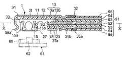
図1及び図2は、本発明に係るコネクタの実施例1を示している。なお、図1では、電線とコネクタとを接続した状態の側面断面図であり、コネクタと接続する相手コネクタの一部を二点鎖線によって示している。図2は、図1に示したコネクタの概観を側面から見た図である。図3は、図2に示したコネクタをIII-III線によって断面した図である。 1 and 2 show a first embodiment of a connector according to the present invention. In addition, in FIG. 1, it is side surface sectional drawing of the state which connected the electric wire and the connector, and a part of mating connector connected with a connector is shown with the dashed-two dotted line. FIG. 2 is a side view of the connector shown in FIG. FIG. 3 is a cross-sectional view of the connector shown in FIG. 2 taken along line III-III.
図1乃至図3を参照して、コネクタ1は、導電性のコンタクト11と、コンタクト11を保持している絶縁性のハウジング21と、ハウジング21の外側に配設されている導電性の外部コンタクト31とを有する。 1 to 3, the
なお、図1乃至図3に示した実施例1おけるコネクタ1には、電線51が芯線52と、芯線52を覆っている誘電体53と、誘電体53を覆っている外部導体54と、外部導体54を覆っている絶縁性の外皮55とからなる。 The
図4に示したコネクタ1は、電線51を接続する前の形態を示している。図5は、コンタクト11を示している。コンタクト11は、図4及び図5にも示すように、略長板状の基部12と、電線51の芯線52に接続するように軸X(図1を参照)方向の基部12の一端部側に形成されている結線部13と、基部12の軸X方向の他端部側に形成されている接触部15とを有する。 The
結線部13は、基部12の長手方向と平行な基部12の一辺から突出しており、かつ軸X方向に形成されている2つの突起状の圧接刃13a、13bを有する。図6及び図7にも示すように、2つの圧接刃13a、13bの先端部のそれぞれには、板厚面にテーパー部13e、13fが形成されている。 The connecting
図6によって明らかなように、テーパー部13e、13fのそれぞれは、紙面の右側面から見ると互いに交差する方向に形成されている。即ち、一方のテーパー部13eは軸X方向と直交する板厚面の一側に形成されており、他方のテーパー部13fは、軸X方向と直交する板厚面の他側に形成される。なお、図6及び図7によって明らかなように、テーパー部13e,13fは、コンタクト11の板厚寸法の範囲内に形成されている。 As is apparent from FIG. 6, each of the
接触部15は、基部12の一辺から相対向するように延びている一対のバネ片15a,15bを有する。バネ片15a,15bは、コンタクト11の板厚寸法と同じ板厚寸法となっている。 The
図1乃至図4に戻り、ハウジング21は、電線51の芯線52と結線部13とを接続させるために軸X方向の一端部側に形成されている一対の覆い部23、24と、電線51を収容するために一対の覆い部23、24に連設されている収容部26と、軸X方向の他端部側に形成されている略溝状の嵌合部27とを有する。 Returning to FIGS. 1 to 4, the
収容部26には、ハウジング21の外側から挿通されて収容部26内に結線部13が配設されている。収容部26は電線51の芯線52を覆う誘電体53を圧入して位置決めするための第1の位置決め部26aと、芯線52を覆う誘電体53を第1の位置決め部26aに位置決めしておくための一対の第2の位置決め部26bとを有する。 A connecting
第1の位置決め部26aは、断面略U字状に形成されている収容部26の内側壁部である。一対の第2の位置決め部26bは、収容部26の一対の内側壁部の開口端から相対向するように突出している突部となっている。なお、収容部26において第1の位置決め部26aを構成している一対の内側壁部間の幅寸法は、誘電体53の直径よりも少し小さい間隔となっている。また、第2の位置決め部26bの間隔は、収容部26の一対の内側壁部間の幅寸法よりも狭い間隔となっている。また、一対の第2の位置決め部26bと、誘電体53とが接触する部分と、収容部26を構成しているハウジング底部21aの内面からの高さ寸法は、誘電体53の直径よりも少し小さい寸法となっている。 The
嵌合部27には、コンタクト11の接触部15が位置している。接触部15の一対のバネ片15a,15b間には、図1に示した相手コネクタ61に配設されている相手接触部62が入り込み嵌合することによって接続する。相手コネクタ61には、嵌合部27を受け入れる導電性の相手嵌合部65が形成されている。 The
外部コンタクト31は、軸X方向の一端側で底部32の長手方向と平行な二辺から相対向きするように延びている一対の外皮保持部35a,35bと、一対の外皮保持部35a,35bと間隔をもって隣接しかつ底部32の長手方向と平行な二辺から相対向するように延びている一対の外部導体保持部36a,36bとを有する。 The
さらに、外部コンタクト31は、外部導体保持部36a,36bと間隔をもって隣接しかつ底部32の長手方向と平行な二辺から相対向するように延びている一対の誘電体保持部37a,37bと、誘電体保持部37a,37bと間隔をもって隣接しかつ底部32から略筒状に延びている略筒状の嵌合枠部38とを有している。 Further, the
一対の誘電体保持部37a,37bの内側には、ハウジング21の覆い部23,24が位置している。一対の誘電体保持部37a,37bを連設している底部32は、収容部26のハウジング底部21aと対向するように位置している。 The
嵌合枠部38の先端辺には、嵌合部27に対向するように突出しているバネ突部38aが形成されている。嵌合枠部38は、図1に示した相手コネクタ61の相手嵌合部65の外面にバネ突部38aの内面が接触する。 A
上述したように、コネクタ1は、コンタクト11の結線部13と電線51の芯線52とが接続し、コンタクト11と外部コンタクト31とがハウジング21を介して絶縁された状態で配設されている。 As described above, the
コンタクト11は、たとえば、相手コネクタ61を介して相手コネクタ61を実装しているプリント配線基板(図示せず)の回路と接続させることによって信号を送受する。また、外部コンタクト31は、相手嵌合部65と嵌合し相手コネクタ61を実装しているプリント配線基板のアース回路と接続させることによってアースする役目を果たす。 The
なお、コンタクト11は、導電板を打ち抜きプレス加工することによって作ることができる。ハウジング21は、樹脂材により成形加工することによって作ることができる。外部コンタクト31は、導電板を打ち抜きプレス加工した後に、曲げ加工を施すことによって作ることができる。 The
以下、図8乃至図12をも参照して、コネクタ1と同軸ケーブル51との接続について説明する。なお、図8に示したコネクタ1は、図4に示したコネクタ1のVIII-VIII線断面を示している。 Hereinafter, the connection between the
図8に示すように、接続前のコネクタ1と電線51とを接続する際には、軸X方向の他端部の電線51の部分において、外部導体54及び誘電体53が露出するように外皮55及び外部導体54を取り除いておく。 As shown in FIG. 8, when connecting the
次に、図9及び図10に示すように、電線51の外皮55を外皮保持部35a,35b間に位置させ、外部導体54を外部導体保持部36a,36b間に位置させ、さらに、誘電体53をハウジング21の収容部26上にかつ覆い部23,24間に位置させる。 Next, as shown in FIGS. 9 and 10, the
図10の状態から、覆い部23,24のそれぞれを内向きに倒し込み、誘電体53を覆い部23,24によって押圧しながら誘電体53を収容部26へ押し込む。誘電体53は第2の位置決め部26b間で圧縮されながら、結線部13の2つの圧接刃13a、13bの板厚の中心と電線51の芯線52が位置合わせされた状態で通過して収容部26へ収容される。この際、誘電体53は第1の位置決め部26aと第2の位置決め部26bとによって誘電体53が収容部26内に確実に保持される。 From the state of FIG. 10, each of the
電線51の誘電体53が収容部26内に押し込まれるときには、図11及び図12に示すように、結線部13の圧接刃13a,13bは誘電体53を突き破り、図3に示した芯線52と圧接して確実に接続する。 When the dielectric 53 of the
前述したように、一対の第2の位置決め部26a,26b間の寸法は、収容部26の内壁部の側壁部間の寸法よりも少し小さい寸法となっており、しかも誘電体53の直径寸法よりも少し小さく設定されているので、電線51の芯線52を圧接刃13a,13bの位置へと確実に誘導させることができる。また、覆い部23,24は、芯線52が圧接刃13a,13bに接続した状態で、第1及び第2の位置決め部26a,26bとによって、しっかりと誘電体53を保持する。 As described above, the dimension between the pair of
図10に示すように、多い分23,24のそれぞれに形成した括れ部23a,24aの構成により、覆い部23,24を内向きに倒し込んだ後、押圧を解除しても元の位置に戻ることはない。 As shown in FIG. 10, the
なお、実施例において、2つの覆い部23,24によって誘電体53を押圧するようにしているが、2つ以上の覆い部をハウジング21に形成するようにしてもよい。また、結線部13の2つの圧接刃13a,13bは、1つ若しくは2つ以上を軸X方向へ形成するようにしてもよい。 In the embodiment, the dielectric 53 is pressed by the two
さらに、電線51は、外皮保持部35a,35bにより外皮55を囲むように曲げて押圧することによって外皮55が外皮保持部35a,35bに保持され、外部導体54を外部導体保持部36a,36bによって囲むように曲げて押圧することによって外部導体54が外部導体保持部36a,36bに保持され、ハウジング21の収容部26上の覆い部23,24を誘電体保持部37a,37bによって囲むように曲げて押圧することによって誘電体53が誘電体保持部37a,37bに保持される。 Further, the
なお、本実施例では、外部コンタクト31の外皮保持部35a,35bと外部導体保持部36a,36bと誘電体保持部37a,37b及びコンタクト11の結線部13と電線51を一括、即ち、同時に圧着して接続することができる。 In the present embodiment, the outer
図13は、コネクタ1の実施例2を示している。このコネクタ1では、コンタクト11の結線部13の形状のみが異なるため、他の部分の構成については、同じ符号を付して説明する。 FIG. 13 shows a second embodiment of the
コンタクト11の基部12には、結線部13が形成されている。結線部13は、基部12から延びている圧接刃13hを有する。基部12の板厚方向と直交する方向に圧接刃13hの板厚方向が形成されている。即ち、圧接刃13hの根元を基部12から90度の角度でねじり曲げることにより、圧接刃13を形成する。圧接刃13hの板面には、上端から下方へスリット13jが形成されている。 A
図9に示すように、電線51の外皮55を外皮保持部35a,35b間に位置させ、外部導体54を外部導体保持部36a,36bに位置させ、さらに、誘電体53をハウジング21の収容部26上にかつ覆い部23,24間に位置させる。 As shown in FIG. 9, the
次に、覆い部23,24を内向きに倒し込みながら、図14の状態から誘電体53を覆い部23,24によって押圧することにより、誘電体53を収容部26へ押し込むと誘電体53が収容部26へ収容される。この際、誘電体53は第1の位置決め部26aと第2の位置決め部26bとによって誘電体53が収容部26内に確実に保持される。このように誘電体53が収容部26内に押し込まれるときには、図15に示すように、圧接刃13hは誘電体53を突き破り、芯線52と接続する。 Next, when the dielectric 53 is pushed into the
この際、一対の第2の位置決め部26a,26b間の寸法は、収容部26の内壁部の側壁部間の寸法よりも少し小さい寸法となっており、しかも誘電体53の直径寸法よりも少し小さく設定されているので、電線51の芯線52が圧接刃13hのスリット13jを中心として確実に誘導させることができる。 At this time, the dimension between the pair of
また、覆い部23,24は、芯線52がスリット13jを中心として結線部13に接続した状態で、第1及び第2の位置決め部26a,26bとによりしっかりと誘電体53を保持できる。 Moreover, the
本発明のコネクタは、芯線を被覆した外皮を有するケーブルと相手コネクタとを機器内で接続する用途に適用できる。 The connector of the present invention can be applied to an application in which a cable having a sheath coated with a core wire and a mating connector are connected in a device.
1 コネクタ
11 コンタクト
12 基部
13,13h 結線部
15 接触部
13a、13b 圧接刃
13e、13f テーパー部
13j スリット
15a,15b バネ片
21 ハウジング
23、24 覆い部
26 収容部
27 嵌合部
26a 第1の位置決め部
26b 第2の位置決め部
31 外部コンタクト
32 底部
35a,35b 外皮保持部
36a,36b 外部導体保持部
37a,37b 誘電体保持部
38 嵌合枠部
51 電線
52 芯線
53 誘電体
54 外部導体
55 外皮
61 相手コネクタDESCRIPTION OF
Claims (2)
Translated fromJapanesePriority Applications (4)
| Application Number | Priority Date | Filing Date | Title |
|---|---|---|---|
| JP2007023244AJP4097681B1 (en) | 2007-02-01 | 2007-02-01 | connector |
| CN2008800011371ACN101569062B (en) | 2007-02-01 | 2008-01-30 | Connector |
| PCT/JP2008/051422WO2008093739A1 (en) | 2007-02-01 | 2008-01-30 | Connector |
| US12/312,116US7833054B2 (en) | 2007-02-01 | 2008-01-30 | Connector |
Applications Claiming Priority (1)
| Application Number | Priority Date | Filing Date | Title |
|---|---|---|---|
| JP2007023244AJP4097681B1 (en) | 2007-02-01 | 2007-02-01 | connector |
Publications (2)
| Publication Number | Publication Date |
|---|---|
| JP4097681B1true JP4097681B1 (en) | 2008-06-11 |
| JP2008192369A JP2008192369A (en) | 2008-08-21 |
Family
ID=39560821
Family Applications (1)
| Application Number | Title | Priority Date | Filing Date |
|---|---|---|---|
| JP2007023244AExpired - Fee RelatedJP4097681B1 (en) | 2007-02-01 | 2007-02-01 | connector |
Country Status (4)
| Country | Link |
|---|---|
| US (1) | US7833054B2 (en) |
| JP (1) | JP4097681B1 (en) |
| CN (1) | CN101569062B (en) |
| WO (1) | WO2008093739A1 (en) |
Cited By (8)
| Publication number | Priority date | Publication date | Assignee | Title |
|---|---|---|---|---|
| US7945106B2 (en) | 2003-09-23 | 2011-05-17 | Thomson Licensing | Method for simulating film grain by mosaicing pre-computer samples |
| US8238613B2 (en) | 2003-10-14 | 2012-08-07 | Thomson Licensing | Technique for bit-accurate film grain simulation |
| US8472526B2 (en) | 2004-11-23 | 2013-06-25 | Thomson Licensing | Low-complexity film grain simulation technique |
| US8483288B2 (en) | 2004-11-22 | 2013-07-09 | Thomson Licensing | Methods, apparatus and system for film grain cache splitting for film grain simulation |
| US9098916B2 (en) | 2004-11-17 | 2015-08-04 | Thomson Licensing | Bit-accurate film grain simulation method based on pre-computed transformed coefficients |
| US9117261B2 (en) | 2004-11-16 | 2015-08-25 | Thomson Licensing | Film grain SEI message insertion for bit-accurate simulation in a video system |
| US9177364B2 (en) | 2004-11-16 | 2015-11-03 | Thomson Licensing | Film grain simulation method based on pre-computed transform coefficients |
| US10715834B2 (en) | 2007-05-10 | 2020-07-14 | Interdigital Vc Holdings, Inc. | Film grain simulation based on pre-computed transform coefficients |
Families Citing this family (13)
| Publication number | Priority date | Publication date | Assignee | Title |
|---|---|---|---|---|
| JP4730415B2 (en)* | 2008-09-10 | 2011-07-20 | 株式会社村田製作所 | L-type coaxial connector |
| JP4720881B2 (en)* | 2008-09-10 | 2011-07-13 | 株式会社村田製作所 | L-type coaxial connector |
| JP5336963B2 (en)* | 2009-07-22 | 2013-11-06 | 日本航空電子工業株式会社 | connector |
| JP5523154B2 (en)* | 2010-03-18 | 2014-06-18 | 日本圧着端子製造株式会社 | Coaxial connector and board connector |
| CN102842838B (en)* | 2012-08-01 | 2015-01-07 | 番禺得意精密电子工业有限公司 | Cable connector and manufacturing method thereof |
| CN105098456B (en)* | 2014-04-23 | 2017-11-07 | 春源科技(深圳)有限公司 | Cover-lifting type plate terminal adapter and arranged in pairs or groups with it flat cables of RF used and line-end connector |
| JP5949838B2 (en) | 2014-06-16 | 2016-07-13 | 第一精工株式会社 | Coaxial electrical connector |
| JP6379403B2 (en)* | 2014-12-02 | 2018-08-29 | ヒロセ電機株式会社 | Coaxial cable connector with core wire holding and fixing function |
| CN104409901B (en)* | 2014-12-12 | 2017-02-22 | 昆山嘉华电子有限公司 | Coaxial cable connector |
| JP6758645B2 (en)* | 2016-10-28 | 2020-09-23 | 日本圧着端子製造株式会社 | Piercing contacts and coaxial connectors |
| DE102019117473A1 (en)* | 2019-06-28 | 2020-12-31 | Tesat-Spacecom Gmbh & Co. Kg | Circuit arrangement consisting of two interconnected high-frequency components |
| JP7404142B2 (en)* | 2020-04-17 | 2023-12-25 | 日本航空電子工業株式会社 | Connectors, harnesses and connector assemblies |
| JP7716079B2 (en)* | 2021-03-05 | 2025-07-31 | 日本圧着端子製造株式会社 | Coaxial Connectors |
Family Cites Families (3)
| Publication number | Priority date | Publication date | Assignee | Title |
|---|---|---|---|---|
| JP2665717B2 (en)* | 1993-10-06 | 1997-10-22 | 日本航空電子工業株式会社 | Coaxial connector plug |
| JPH0822851A (en)* | 1994-07-07 | 1996-01-23 | Japan Aviation Electron Ind Ltd | Coaxial plug connector |
| JPH1126037A (en)* | 1997-06-30 | 1999-01-29 | Yazaki Corp | Terminal conductor connection structure |
- 2007
- 2007-02-01JPJP2007023244Apatent/JP4097681B1/ennot_activeExpired - Fee Related
- 2008
- 2008-01-30USUS12/312,116patent/US7833054B2/ennot_activeExpired - Fee Related
- 2008-01-30WOPCT/JP2008/051422patent/WO2008093739A1/enactiveApplication Filing
- 2008-01-30CNCN2008800011371Apatent/CN101569062B/ennot_activeExpired - Fee Related
Cited By (8)
| Publication number | Priority date | Publication date | Assignee | Title |
|---|---|---|---|---|
| US7945106B2 (en) | 2003-09-23 | 2011-05-17 | Thomson Licensing | Method for simulating film grain by mosaicing pre-computer samples |
| US8238613B2 (en) | 2003-10-14 | 2012-08-07 | Thomson Licensing | Technique for bit-accurate film grain simulation |
| US9117261B2 (en) | 2004-11-16 | 2015-08-25 | Thomson Licensing | Film grain SEI message insertion for bit-accurate simulation in a video system |
| US9177364B2 (en) | 2004-11-16 | 2015-11-03 | Thomson Licensing | Film grain simulation method based on pre-computed transform coefficients |
| US9098916B2 (en) | 2004-11-17 | 2015-08-04 | Thomson Licensing | Bit-accurate film grain simulation method based on pre-computed transformed coefficients |
| US8483288B2 (en) | 2004-11-22 | 2013-07-09 | Thomson Licensing | Methods, apparatus and system for film grain cache splitting for film grain simulation |
| US8472526B2 (en) | 2004-11-23 | 2013-06-25 | Thomson Licensing | Low-complexity film grain simulation technique |
| US10715834B2 (en) | 2007-05-10 | 2020-07-14 | Interdigital Vc Holdings, Inc. | Film grain simulation based on pre-computed transform coefficients |
Also Published As
| Publication number | Publication date |
|---|---|
| JP2008192369A (en) | 2008-08-21 |
| CN101569062A (en) | 2009-10-28 |
| WO2008093739A1 (en) | 2008-08-07 |
| US7833054B2 (en) | 2010-11-16 |
| CN101569062B (en) | 2012-03-28 |
| US20100022122A1 (en) | 2010-01-28 |
Similar Documents
| Publication | Publication Date | Title |
|---|---|---|
| JP4097681B1 (en) | connector | |
| KR101375039B1 (en) | Coaxial connector apparatus | |
| JP4274381B2 (en) | Terminal connection method for micro coaxial cable | |
| US8734179B2 (en) | Cable connector and manufacturing method thereof | |
| KR101353660B1 (en) | Coaxial electrical connector and coaxial electrical connector assembly | |
| US8007325B2 (en) | Cable connecting apparatus | |
| JP5772900B2 (en) | Coaxial electrical connector | |
| JP2011060770A (en) | Capped insulation displacement connector | |
| KR20120049219A (en) | Coaxial connector and method for assembling the same | |
| JP4440160B2 (en) | connector | |
| KR101743390B1 (en) | Coaxial electrical connector | |
| JP2018073597A (en) | Piercing contacts and coaxial connectors | |
| JP2006269150A (en) | Method for manufacturing terminal fitting and terminal fitting | |
| KR101521386B1 (en) | Method of connecting a cable with a cable connector | |
| JP2009048941A (en) | Connector device | |
| JP2019220253A (en) | Coaxial connector | |
| JP4977768B2 (en) | Manufacturing method of multiple types of terminal fittings | |
| JP2010067478A (en) | Terminal fitting, and electric wire with terminal fitting | |
| KR101035932B1 (en) | Automotive Electrical Connector Box | |
| JP2007280765A (en) | Electrical connector | |
| JP4102295B2 (en) | Piercing terminal for coaxial cable | |
| JPH11121108A (en) | Electrical connector for circuit board | |
| JP2006236873A (en) | Method for manufacturing terminal fitting and terminal fitting | |
| JP2020009600A (en) | Wire and terminal connection structure | |
| JPH0822851A (en) | Coaxial plug connector |
Legal Events
| Date | Code | Title | Description |
|---|---|---|---|
| TRDD | Decision of grant or rejection written | ||
| A01 | Written decision to grant a patent or to grant a registration (utility model) | Free format text:JAPANESE INTERMEDIATE CODE: A01 Effective date:20080305 | |
| A61 | First payment of annual fees (during grant procedure) | Free format text:JAPANESE INTERMEDIATE CODE: A61 Effective date:20080311 | |
| R150 | Certificate of patent or registration of utility model | Ref document number:4097681 Country of ref document:JP Free format text:JAPANESE INTERMEDIATE CODE: R150 Free format text:JAPANESE INTERMEDIATE CODE: R150 | |
| FPAY | Renewal fee payment (event date is renewal date of database) | Free format text:PAYMENT UNTIL: 20110321 Year of fee payment:3 | |
| FPAY | Renewal fee payment (event date is renewal date of database) | Free format text:PAYMENT UNTIL: 20120321 Year of fee payment:4 | |
| FPAY | Renewal fee payment (event date is renewal date of database) | Free format text:PAYMENT UNTIL: 20120321 Year of fee payment:4 | |
| FPAY | Renewal fee payment (event date is renewal date of database) | Free format text:PAYMENT UNTIL: 20120321 Year of fee payment:4 | |
| FPAY | Renewal fee payment (event date is renewal date of database) | Free format text:PAYMENT UNTIL: 20130321 Year of fee payment:5 | |
| R250 | Receipt of annual fees | Free format text:JAPANESE INTERMEDIATE CODE: R250 | |
| FPAY | Renewal fee payment (event date is renewal date of database) | Free format text:PAYMENT UNTIL: 20130321 Year of fee payment:5 | |
| FPAY | Renewal fee payment (event date is renewal date of database) | Free format text:PAYMENT UNTIL: 20130321 Year of fee payment:5 | |
| FPAY | Renewal fee payment (event date is renewal date of database) | Free format text:PAYMENT UNTIL: 20140321 Year of fee payment:6 | |
| R250 | Receipt of annual fees | Free format text:JAPANESE INTERMEDIATE CODE: R250 | |
| R250 | Receipt of annual fees | Free format text:JAPANESE INTERMEDIATE CODE: R250 | |
| R250 | Receipt of annual fees | Free format text:JAPANESE INTERMEDIATE CODE: R250 | |
| R250 | Receipt of annual fees | Free format text:JAPANESE INTERMEDIATE CODE: R250 | |
| R250 | Receipt of annual fees | Free format text:JAPANESE INTERMEDIATE CODE: R250 | |
| R250 | Receipt of annual fees | Free format text:JAPANESE INTERMEDIATE CODE: R250 | |
| R250 | Receipt of annual fees | Free format text:JAPANESE INTERMEDIATE CODE: R250 | |
| LAPS | Cancellation because of no payment of annual fees |