JP4096359B2 - Manufacturing equipment for manufacturing objects - Google Patents
Manufacturing equipment for manufacturing objectsDownload PDFInfo
- Publication number
- JP4096359B2 JP4096359B2JP2003063785AJP2003063785AJP4096359B2JP 4096359 B2JP4096359 B2JP 4096359B2JP 2003063785 AJP2003063785 AJP 2003063785AJP 2003063785 AJP2003063785 AJP 2003063785AJP 4096359 B2JP4096359 B2JP 4096359B2
- Authority
- JP
- Japan
- Prior art keywords
- wafer
- manufacturing
- conveyor
- manufacturing object
- processing apparatus
- Prior art date
- Legal status (The legal status is an assumption and is not a legal conclusion. Google has not performed a legal analysis and makes no representation as to the accuracy of the status listed.)
- Expired - Fee Related
Links
- 238000004519manufacturing processMethods0.000titleclaimsdescription239
- 238000000034methodMethods0.000claimsdescription33
- 239000000047productSubstances0.000claimsdescription18
- 239000004065semiconductorSubstances0.000claimsdescription14
- 239000013067intermediate productSubstances0.000claimsdescription5
- 235000012431wafersNutrition0.000description156
- 238000012546transferMethods0.000description110
- 238000007689inspectionMethods0.000description16
- 238000005229chemical vapour depositionMethods0.000description5
- 230000003749cleanlinessEffects0.000description5
- 239000000428dustSubstances0.000description3
- 241000406668Loxodonta cyclotisSpecies0.000description1
- 238000004140cleaningMethods0.000description1
- 238000005530etchingMethods0.000description1
- 238000009434installationMethods0.000description1
- 239000004973liquid crystal related substanceSubstances0.000description1
- 238000001459lithographyMethods0.000description1
- 238000012986modificationMethods0.000description1
- 230000004048modificationEffects0.000description1
- 230000002093peripheral effectEffects0.000description1
- 238000013404process transferMethods0.000description1
- 238000007789sealingMethods0.000description1
- 239000000758substrateSubstances0.000description1
Images


Classifications
- E—FIXED CONSTRUCTIONS
- E03—WATER SUPPLY; SEWERAGE
- E03F—SEWERS; CESSPOOLS
- E03F3/00—Sewer pipe-line systems
- E03F3/04—Pipes or fittings specially adapted to sewers
- H—ELECTRICITY
- H01—ELECTRIC ELEMENTS
- H01L—SEMICONDUCTOR DEVICES NOT COVERED BY CLASS H10
- H01L21/00—Processes or apparatus adapted for the manufacture or treatment of semiconductor or solid state devices or of parts thereof
- H01L21/67—Apparatus specially adapted for handling semiconductor or electric solid state devices during manufacture or treatment thereof; Apparatus specially adapted for handling wafers during manufacture or treatment of semiconductor or electric solid state devices or components ; Apparatus not specifically provided for elsewhere
- H01L21/677—Apparatus specially adapted for handling semiconductor or electric solid state devices during manufacture or treatment thereof; Apparatus specially adapted for handling wafers during manufacture or treatment of semiconductor or electric solid state devices or components ; Apparatus not specifically provided for elsewhere for conveying, e.g. between different workstations
- H01L21/67703—Apparatus specially adapted for handling semiconductor or electric solid state devices during manufacture or treatment thereof; Apparatus specially adapted for handling wafers during manufacture or treatment of semiconductor or electric solid state devices or components ; Apparatus not specifically provided for elsewhere for conveying, e.g. between different workstations between different workstations
- H01L21/67727—Apparatus specially adapted for handling semiconductor or electric solid state devices during manufacture or treatment thereof; Apparatus specially adapted for handling wafers during manufacture or treatment of semiconductor or electric solid state devices or components ; Apparatus not specifically provided for elsewhere for conveying, e.g. between different workstations between different workstations using a general scheme of a conveying path within a factory
- H—ELECTRICITY
- H01—ELECTRIC ELEMENTS
- H01L—SEMICONDUCTOR DEVICES NOT COVERED BY CLASS H10
- H01L21/00—Processes or apparatus adapted for the manufacture or treatment of semiconductor or solid state devices or of parts thereof
- H01L21/67—Apparatus specially adapted for handling semiconductor or electric solid state devices during manufacture or treatment thereof; Apparatus specially adapted for handling wafers during manufacture or treatment of semiconductor or electric solid state devices or components ; Apparatus not specifically provided for elsewhere
- H01L21/677—Apparatus specially adapted for handling semiconductor or electric solid state devices during manufacture or treatment thereof; Apparatus specially adapted for handling wafers during manufacture or treatment of semiconductor or electric solid state devices or components ; Apparatus not specifically provided for elsewhere for conveying, e.g. between different workstations
- H01L21/67703—Apparatus specially adapted for handling semiconductor or electric solid state devices during manufacture or treatment thereof; Apparatus specially adapted for handling wafers during manufacture or treatment of semiconductor or electric solid state devices or components ; Apparatus not specifically provided for elsewhere for conveying, e.g. between different workstations between different workstations
- H01L21/67736—Loading to or unloading from a conveyor
- H—ELECTRICITY
- H01—ELECTRIC ELEMENTS
- H01L—SEMICONDUCTOR DEVICES NOT COVERED BY CLASS H10
- H01L21/00—Processes or apparatus adapted for the manufacture or treatment of semiconductor or solid state devices or of parts thereof
- H01L21/67—Apparatus specially adapted for handling semiconductor or electric solid state devices during manufacture or treatment thereof; Apparatus specially adapted for handling wafers during manufacture or treatment of semiconductor or electric solid state devices or components ; Apparatus not specifically provided for elsewhere
- H01L21/677—Apparatus specially adapted for handling semiconductor or electric solid state devices during manufacture or treatment thereof; Apparatus specially adapted for handling wafers during manufacture or treatment of semiconductor or electric solid state devices or components ; Apparatus not specifically provided for elsewhere for conveying, e.g. between different workstations
- H01L21/67763—Apparatus specially adapted for handling semiconductor or electric solid state devices during manufacture or treatment thereof; Apparatus specially adapted for handling wafers during manufacture or treatment of semiconductor or electric solid state devices or components ; Apparatus not specifically provided for elsewhere for conveying, e.g. between different workstations the wafers being stored in a carrier, involving loading and unloading
- H01L21/67766—Mechanical parts of transfer devices
- F—MECHANICAL ENGINEERING; LIGHTING; HEATING; WEAPONS; BLASTING
- F16—ENGINEERING ELEMENTS AND UNITS; GENERAL MEASURES FOR PRODUCING AND MAINTAINING EFFECTIVE FUNCTIONING OF MACHINES OR INSTALLATIONS; THERMAL INSULATION IN GENERAL
- F16L—PIPES; JOINTS OR FITTINGS FOR PIPES; SUPPORTS FOR PIPES, CABLES OR PROTECTIVE TUBING; MEANS FOR THERMAL INSULATION IN GENERAL
- F16L25/00—Construction or details of pipe joints not provided for in, or of interest apart from, groups F16L13/00 - F16L23/00
- F16L25/0036—Joints for corrugated pipes
- F16L25/0063—Joints for corrugated pipes with two corrugated pipes being directly connected to each other
- Y—GENERAL TAGGING OF NEW TECHNOLOGICAL DEVELOPMENTS; GENERAL TAGGING OF CROSS-SECTIONAL TECHNOLOGIES SPANNING OVER SEVERAL SECTIONS OF THE IPC; TECHNICAL SUBJECTS COVERED BY FORMER USPC CROSS-REFERENCE ART COLLECTIONS [XRACs] AND DIGESTS
- Y10—TECHNICAL SUBJECTS COVERED BY FORMER USPC
- Y10T—TECHNICAL SUBJECTS COVERED BY FORMER US CLASSIFICATION
- Y10T29/00—Metal working
- Y10T29/53—Means to assemble or disassemble
- Y10T29/5313—Means to assemble electrical device
- Y10T29/53174—Means to fasten electrical component to wiring board, base, or substrate
- Y10T29/53178—Chip component
- Y—GENERAL TAGGING OF NEW TECHNOLOGICAL DEVELOPMENTS; GENERAL TAGGING OF CROSS-SECTIONAL TECHNOLOGIES SPANNING OVER SEVERAL SECTIONS OF THE IPC; TECHNICAL SUBJECTS COVERED BY FORMER USPC CROSS-REFERENCE ART COLLECTIONS [XRACs] AND DIGESTS
- Y10—TECHNICAL SUBJECTS COVERED BY FORMER USPC
- Y10T—TECHNICAL SUBJECTS COVERED BY FORMER US CLASSIFICATION
- Y10T29/00—Metal working
- Y10T29/53—Means to assemble or disassemble
- Y10T29/5313—Means to assemble electrical device
- Y10T29/53187—Multiple station assembly apparatus
- Y—GENERAL TAGGING OF NEW TECHNOLOGICAL DEVELOPMENTS; GENERAL TAGGING OF CROSS-SECTIONAL TECHNOLOGIES SPANNING OVER SEVERAL SECTIONS OF THE IPC; TECHNICAL SUBJECTS COVERED BY FORMER USPC CROSS-REFERENCE ART COLLECTIONS [XRACs] AND DIGESTS
- Y10—TECHNICAL SUBJECTS COVERED BY FORMER USPC
- Y10T—TECHNICAL SUBJECTS COVERED BY FORMER US CLASSIFICATION
- Y10T29/00—Metal working
- Y10T29/53—Means to assemble or disassemble
- Y10T29/5313—Means to assemble electrical device
- Y10T29/53261—Means to align and advance work part
Landscapes
- Engineering & Computer Science (AREA)
- Microelectronics & Electronic Packaging (AREA)
- Condensed Matter Physics & Semiconductors (AREA)
- General Physics & Mathematics (AREA)
- Manufacturing & Machinery (AREA)
- Computer Hardware Design (AREA)
- Physics & Mathematics (AREA)
- Power Engineering (AREA)
- Robotics (AREA)
- Health & Medical Sciences (AREA)
- Life Sciences & Earth Sciences (AREA)
- Hydrology & Water Resources (AREA)
- Public Health (AREA)
- Water Supply & Treatment (AREA)
- Container, Conveyance, Adherence, Positioning, Of Wafer (AREA)
Description
Translated fromJapanese【0001】
【発明の属する技術分野】
本発明は、たとえば半導体ウェハのような製造対象物の製造装置および製造対象物の製造方法に関するものである。
【0002】
【従来の技術】
たとえば、半導体ウェハ(以下ウェハという)を製造するための半導体処理装置は、たとえばリソグラフィー装置、成膜装置、エッチング装置、洗浄装置、検査装置等の各種のウェハ処理装置を有している。
このようなウェハ処理装置の間にウェハを移動するために、ウェハカセットが用いられる。このウェハカセットは、複数枚のウェハを着脱可能に収納するものである。このウェハカセットには、工程搬送系からから要求されるロットに応じて複数枚のウェハが収容される(たとえば特許文献1)。
また、ウェハカセット方式によるウェハの搬送に代えて、少量多品種生産の要求から、コンベアに対してウェハを一枚ずつ置いて搬送するいわゆる枚葉搬送の考え方が出てきている。この枚葉搬送方式はウェハの少量多品種生産に対応させたものである(たとえば特許文献2)。
【0003】
【特許文献1】
特開昭62−48038号公報(第2頁、図1参照)
【特許文献2】
特開2002−334917号公報(第1頁、図1参照)
【0004】
【発明が解決しようとする課題】
ところがこのような枚葉搬送方式を採用すると次のような問題がある。
1つの枚葉搬送方式のコンベアは、複数の処理装置に対応して配置されている。すなわちこの枚葉搬送コンベアは、各処理装置に対して枚葉搬送方式でウェハを供給する。枚葉搬送コンベアと複数の処理装置が1つの工程を構成している。
またその隣には、別の工程が配置されている。この工程にはやはり枚葉搬送コンベアと複数の処理装置が配置される。このような複数の工程が並んでいる製造システムの場合には、隣接の各工程において同じ処理機能を有する処理装置が存在している。
この処理装置はたとえば膜厚検査装置である。膜厚検査装置は、1台で2つの隣接する工程におけるウェハの膜厚検査処理を全てまかなえるほど、膜厚検査処理能力が高い。
【0005】
したがって、このような処理能力が比較的低いたとえばCVD(化学気相成長)装置のような処理装置と、処理能力が比較的高いたとえば膜厚検査装置のような処理装置が、各工程の枚葉搬送コンベアに重複して配置されている。装置の数が多いので、投資額が増大してしまう。
そして一方の枚葉搬送コンベアから他方の枚葉搬送コンベアへウェハを送りたい場合には、一度ウェハはカセットに格納する。このカセットは、工程間搬送コンベアを用いて次の工程に送る。このカセットから再びウェハを取り出して、ウェハは次の工程の枚葉搬送コンベアに移す必要がある。このため、ウェハの詰め替え時間がかなりかかってしまう。したがって、ウェハの製造時間を短縮することができない。
そこで本発明は上記課題を解消し、半導体ウェハのような製造対象物の製造時間を節約することができると共に、処理能力の比較的高い装置を隣接する工程間において共用することにより製造対象物の製造装置の小型化を図れる製造対象物の製造装置および製造対象物の製造方法を提供することを目的としている。
【0006】
【課題を解決するための手段】
本発明の製造対象物の製造装置は、半導体ウェハである製造対象物を搬送して前記製造対象物を複数の処理装置により処理するための製造対象物の製造装置であり、前記処理装置に対して前記製造対象物を枚葉状態で搬送するための複数の枚葉搬送コンベアである搬送手段であり、複数の前記枚葉搬送コンベアは、第1枚葉搬送コンベアと前記第1枚葉搬送コンベアに対して平行に配置された第2枚葉搬送コンベアとを有し、前記処理装置と比較して処理能力の早い装置である共通処理装置は、複数の前記搬送手段の間に配置されて、各前記搬送手段により搬送される前記製造対象物に対して共通の処理を行うための同一の共通処理装置であり、複数の前記搬送手段の間に配置されて、前記共通処理装置と各前記搬送手段との間で、前記製造対象物を受け渡しするための製造対象物の受け渡し部と、を備え、前記製造対象物の受け渡し部は、前記第1枚葉搬送コンベアと前記第2枚葉搬送コンベアの間に配置されており、前記共通処理装置は、前記製造対象物の受け渡し部に対面していることを特徴とする。
【0007】
このような構成によれば、複数の枚葉搬送コンベアである搬送手段は、処理装置に対して製造対象物を枚葉状態で搬送する。そして、複数の前記枚葉搬送コンベアは、第1枚葉搬送コンベアと前記第1枚葉搬送コンベアに対して平行に配置された第2枚葉搬送コンベアとを有している。また、共通処理装置は、前記処理装置と比較して処理能力の早い装置であり、同一の共通処理装置が、複数の搬送手段の間に配置されている。この共通処理装置は、各搬送手段により搬送される製造対象物に対して共通の処理を行うことができる。
製造対象物の受け渡し部は、複数の搬送手段の間に配置されている。この製造対象物の受け渡し部は、共通処理装置と各搬送手段との間で、製造対象物を受け渡しする。
これにより、同一の共通処理装置が複数の搬送手段の間に配置されており、しかも各搬送手段からの製造対象物に対して共通の処理を行うことができる。
したがって、共通処理装置として、比較的処理能力の早い装置を配置することにより、複数の搬送手段でそれぞれ運ばれる製造対象物は効率よく共通して処理して製造時間の節約をすることができる。
しかも、このように共通処理を行う同一の共通処理装置が各搬送手段の間に配置されていることから、それぞれの搬送手段に対して比較的速度の早い処理装置を配置するのに比べて、製造装置の小型化を図ることができる。
また、このような構成によれば、製造対象物は半導体ウェハであり、半導体ウェハの製造時間を節約することができる。
【0011】
このような構成によれば、製造対象物の受け渡し部は、第1枚葉搬送コンベアと第2枚葉搬送コンベアの間に配置されている。共通処理装置は、製造対象物の受け渡し部に対面している。
これにより、製造対象物の受け渡し部は、共通処理装置と第1枚葉搬送コンベアの間と、共通処理装置と第2枚葉搬送コンベアの間において、製造対象物の受け渡しを効率よく行うことができ、製造時間の節約が図れる。
【0012】
また、本発明の製造対象物の製造装置は、半導体ウェハである製造対象物を搬送して前記製造対象物を複数の処理装置により処理するための製造対象物の製造装置であり、前記処理装置に対して前記製造対象物を枚葉状態で搬送するための複数の枚葉搬送コンベアである搬送手段であり、複数の前記枚葉搬送コンベアは、第1枚葉搬送コンベアと前記第1枚葉搬送コンベアに対して平行に配置された第2枚葉搬送コンベアとを有し、前記処理装置と比較して処理能力の早い装置である共通処理装置は、複数の前記搬送手段の間に配置されて、各前記搬送手段により搬送される前記製造対象物に対して共通の処理を行うための同一の共通処理装置であり、複数の前記搬送手段の間に配置されて、前記共通処理装置と各前記搬送手段との間で、前記製造対象物を受け渡しするための製造対象物の受け渡し部と、を備え、前記製造対象物の受け渡し部は、前記第1枚葉搬送コンベアと前記第2枚葉搬送コンベアの間に配置されて前記製造対象物を枚葉搬送する第3枚葉搬送コンベアと、前記第3枚葉搬送コンベアと前記共通処理装置との間で前記第1枚葉搬送コンベア側の前記製造対象物の受け渡しをするとともに、前記第2枚葉搬送コンベアと前記共通処理装置との間で前記製造対象物の受け渡しをするための受け渡し装置とを有することを特徴とすることが望ましい。
【0013】
このような構成によれば、複数の枚葉搬送コンベアである搬送手段は、処理装置に対して製造対象物を枚葉状態で搬送する。そして、複数の前記枚葉搬送コンベアは、第1枚葉搬送コンベアと前記第1枚葉搬送コンベアに対して平行に配置された第2枚葉搬送コンベアとを有している。また、共通処理装置は、前記処理装置と比較して処理能力の早い装置であり、同一の共通処理装置が、複数の搬送手段の間に配置されている。この共通処理装置は、各搬送手段により搬送される製造対象物に対して共通の処理を行うことができる。
製造対象物の受け渡し部は、複数の搬送手段の間に配置されている。この製造対象物の受け渡し部は、共通処理装置と各搬送手段との間で、製造対象物を受け渡しする。
これにより、同一の共通処理装置が複数の搬送手段の間に配置されており、しかも各搬送手段からの製造対象物に対して共通の処理を行うことができる。
したがって、共通処理装置として、比較的処理能力の早い装置を配置することにより、複数の搬送手段でそれぞれ運ばれる製造対象物は効率よく共通して処理して製造時間の節約をすることができる。
しかも、このように共通処理を行う同一の共通処理装置が各搬送手段の間に配置されていることから、それぞれの搬送手段に対して比較的速度の早い処理装置を配置するのに比べて、製造装置の小型化を図ることができる。
また、このような構成によれば、製造対象物は半導体ウェハであり、半導体ウェハの製造時間を節約することができる。
このような構成によれば、製造対象物の受け渡し部の第3枚葉搬送コンベアは、第1枚葉搬送コンベアと第2枚葉搬送コンベアの間に配置されている。受け渡し装置は、第3枚葉搬送コンベアと共通処理装置との間で、第1枚葉搬送コンベア側の製造対象物の受け渡しをする。しかも、受け渡し装置は、第2枚葉搬送コンベアと共通処理装置との間で製造対象物の受け渡しをすることができる。
これにより、第1枚葉搬送コンベアと共通処理装置との間および第2枚葉搬送コンベアと共通処理装置との間で、製造対象物の受け渡しが効率よく行え、製造時間の節約が図れる。
【0019】
【発明の実施の形態】
以下、本発明の好適な実施の形態を図面に基づいて説明する。
図1は、本発明の製造対象物の製造装置を含む製造対象物の製造システムの一部分の例を示す平面図である。この製造対象物の製造システム1は、複数の製造対象物の製造装置10を有している。図1では、1つの製造対象物の製造装置10が例示されている。この製造対象物の製造システム1は、製造対象物としての一例として半導体ウェハW(以下ウェハという)を製造するためのシステムである。
【0020】
第1の実施形態
製造対象物の製造システム1は、図1では、1つの製造対象物の製造装置10と1つのベイ搬送コンベア11を有している。このベイ搬送コンベア11は、工程間搬送コンベアとも呼んでいる。ベイ搬送コンベア11は、たとえば図2に示すような複数のカセット15をR方向にエンドレス状に搬送可能である。
カセット15は、図2に一例を示しており、カセット15は、複数枚のウェハWを着脱可能に収容可能である。このカセット15は、ウェハWを密閉する密閉部分を有しているのが望ましい。複数のカセット15は、図1に示すベイ搬送コンベア11により、工程間で搬送されて工程に供給される。
【0021】
図1に示す製造対象物の製造装置10は、このベイ搬送コンベア11に対して対面して配置されている。図1の例では、1つの製造対象物の製造装置10を示しており、製造対象物の製造装置10は、ベイ搬送コンベア11の一方の側に配置されている。
しかしこれに限らず、1つ又は複数の製造対象物の製造装置10が、ベイ搬送コンベア11の一方の側および図示しないが他方の側に配置されても勿論構わない。
【0022】
製造対象物の製造装置10は、概略的には第1工程B1と第2工程B2および共通処理装置200を有している。工程はベイとも呼んでいる。
第1工程B1と第2工程B2は平行に配置されており、第1工程B1の端部と第2工程B2の端部はベイ搬送コンベア11に接続されている。
第1工程B1は、第1枚葉搬送コンベア20、処理装置23、製造対象物の受け渡しユニット13、製造対象物の受け渡し部100、そしてカセット15のストッカ101を有している。
これに対して第2工程B2は、第2枚葉搬送コンベア120、処理装置123、製造対象物の受け渡しユニット113、製造対象物の受け渡し部103、およびカセット15のストッカ104を有している。
【0023】
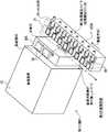
図1に示す第1枚葉搬送コンベア20と第2枚葉搬送コンベア120は、搬送手段の一例であり、それぞれウェハを一枚ずつ枚葉搬送状態で搬送するためのコンベアである。第1枚葉搬送コンベア20と第2枚葉搬送コンベア120は、ウェハWをエンドレス状に搬送方向Tに沿って搬送可能である。第1枚葉搬送コンベア20と第2枚葉搬送コンベア120は同様の構造であり、複数のウェハ保持部46を有している。
図3は、図1に示す第1工程B1の第1枚葉搬送コンベア20と製造対象物の受け渡しユニット13および処理装置23の付近を示す平面図である。図4は、図3に示す第1枚葉搬送コンベア20、製造対象物の受け渡しユニット13および処理装置23の形状例を示す斜視図である。
【0024】
図5は、図1における第2工程B2側の第2枚葉搬送コンベア120、製造対象物の受け渡しユニット113および処理装置123を示している。
第1枚葉搬送コンベア20と第2枚葉搬送コンベア120は、それぞれ枚葉搬送ラインとも呼んでいる。
第1枚葉搬送コンベア20と第2枚葉搬送コンベア120は、同じ構造を有している。図4に示すように、第1枚葉搬送コンベア20は、ベース20Aとそのベース20Aの上に搭載された複数のウェハ保持部46を有している。
複数のウェハ保持部46は、ベース20Aの上において、搬送方向Tに沿ってエンドレス状に配列されている。ウェハ保持部46は、たとえばその上に一枚ずつウェハWを着脱可能に載せるようになっている。各ウェハ保持部46は、等しい間隔を置いて搬送方向Tに沿って配列されていて、図示しない駆動部によりエンドレス状に搬送方向Tに沿って移動可能である。
【0025】
図4に示すように、ベース20Aの上には、クリーントンネル30が設けられている。このクリーントンネル30の上面には、ファン付きフィルタユニット31が設けられている。ファン付きフィルタユニット31は、クリーントンネル30の中に形成された閉空間のクリーン度を高めるために空気の流れ(ダウンフロー)を発生している。これにより、クリーントンネル30内の空気中の塵埃を取り除き、規定された清浄度で管理するようになっている。
このクリーントンネル30は、図4の第1枚葉搬送コンベア20だけではなく図5に示す第2枚葉搬送コンベア120にも設けられている。
【0026】
図1と図3に示す処理装置23は、たとえばCVD(化学気相成長)装置である。この処理装置23は、比較的ウェハWに対する処理能力が低い装置である。つまりこの処理装置23は、ウェハWに対する処理時間が比較的多くかかる装置である。
この処理装置23と第1枚葉搬送コンベア20の間には、図1と図3に示すように製造対象物の受け渡しユニット13が設けられている。
一方、図1と図5に示す処理装置123は、処理装置23と同様のたとえばCVD装置である。処理装置123と第2枚葉搬送コンベア120の間には、製造対象物の受け渡しユニット113が配置されている。
【0027】
ここで、製造対象物の受け渡しユニット13と製造対象物の受け渡しユニット113について構造例を説明する。
製造対象物の受け渡しユニット13は図3に示しており、製造対象物の受け渡しユニット113は図5に示している。
製造対象物の受け渡しユニット13と製造対象物の受け渡しユニット113は同じ構造のものを採用できる。製造対象物の受け渡しユニット13,113は、移載ロボット21と、バッファ34、および本体35を有している。
この本体35は、処理装置23と枚葉搬送コンベア20の間に配置されている。本体35は、上述した移載ロボット21とバッファ34を内部に収容している。
【0028】
図4に示すように、本体35の上部には、ファン付きフィルタユニット(FFU)38が取り付けられている。この本体35は、移載ロボット21とバッファ34を極力小さな閉空間で収容している。ファン付きフィルタユニット38は、この本体35内の空間内にたとえば本体35の上部から下側に向けての空気の流れ(ダウンフロー)を発生させるようになっている。これにより、本体35内の空気中の塵埃を取り除いて、規定された清浄度レベル(清浄度クラス)で本体35内を管理するようになっている。
【0029】
次に、図1に示す共通処理装置200について説明する。
共通処理装置200は、処理装置23と処理装置123に比べて処理能力が比較的高い装置である。共通処理装置200の例としては、たとえば膜厚検査装置である。この膜厚検査装置は、ウェハWに形成された膜の厚みを検査するものである。共通処理装置200は、第1枚葉搬送コンベア20の第1位置P1と第2枚葉搬送コンベア120の第2位置P2の間にある中央位置P3に配置されている。
共通処理装置200は、第1枚葉搬送コンベア20側から送られてくるウェハWと第2枚葉搬送コンベア120側から送られてくるウェハWに対してそれぞれ膜厚検査をするための装置である。
【0030】
次に、図1に示す製造対象物の受け渡し部100,103について説明する。製造対象物の受け渡し部100,103は、それぞれ同じ構造のものを採用できる。製造対象物の受け渡し部100は、第1位置P1に配置されている。製造対象物の受け渡し部103は、第2位置P2に配置されている。
第1位置P1は、第1枚葉搬送コンベア20の側部と中央位置P3の間の位置である。第2位置P2は、第2枚葉搬送コンベア120の側部と中央位置P3の間の位置である。
第1枚葉搬送コンベア20と第2枚葉搬送コンベア120は平行に配置されているが、それぞれ搬送方向Tが逆方向になっている。
【0031】
図6は、製造対象物の受け渡し部100,103および共通処理装置200と、第1枚葉搬送コンベア20および第2枚葉搬送コンベア120の構造例を示す平面図である。
製造対象物の受け渡し部100と製造対象物の受け渡し部103は、同様の構造を有している。製造対象物の受け渡し部100は、移載ロボット221と、バッファ234および本体235を有している。
この本体235は、共通処理装置200と第1枚葉搬送コンベア20の間と、共通処理装置200と第2枚葉搬送コンベア120との間にそれぞれ配置されている。本体235は、上述した移載ロボット221とバッファ234を内部に収容している。
【0032】
図4に示すように、本体235の上部には、ファン付きフィルタユニット(FFU)(図示せず)が取り付けられている。この本体235は、移載ロボット221とバッファ234を極力小さな閉空間で収容している。ファン付きフィルタユニットは、この本体235内の空間内にたとえば本体235の上部から下側に向けての空気の流れ(ダウンフロー)を発生させるようになっている。これにより、本体235内の空気中の塵埃を取り除いて、規定された清浄度レベル(清浄度クラス)で本体235内を管理するようになっている。
製造対象物の受け渡し部100は、第1枚葉搬送コンベア20と、共通処理装置200との間で、ウェハWの受け渡しを行う装置である。製造対象物の受け渡し部103は、第2枚葉搬送コンベア120と共通処理装置200との間でウェハWの受け渡しを行うための装置である。
【0033】
次に、図1に示すストッカ101,104について説明する。
ストッカ101,104は、それぞれ第1枚葉搬送コンベア20と第2枚葉搬送コンベア120に対応して配置されている。ストッカ101は、ベイ搬送コンベア11により搬送されてくるカセット15を一旦ロボット101Aにより取り込む。そしてロボット101Aは、カセット15からウェハWを取り出して第1枚葉搬送コンベア20のウェハ保持部46に対して移載する。またロボット101は、第1枚葉搬送コンベア20により送られてきた処理済みのウェハWを、ストッカ101内のカセット15の中に格納する。そして、必要なウェハWの格納されたカセット15は、ロボット101Aによりストッカ101からベイ搬送コンベア11に戻すことができる。
ストッカ104とストッカ101は同じような構造であり、ストッカ104はロボット104Aを有している。そしてストッカ104はストッカ101と同様な機能を発揮する。
【0034】
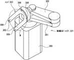
図7と図8は、上述した図3に示す移載ロボット21、図5に示す移載ロボット21、および図6に示す移載ロボット221の構造例を示している。
図3に示す移載ロボット21は、第1枚葉搬送コンベア20と処理装置23の間で、矢印E,E1方向に製造対象物であるウェハWを移載するためのロボットである。図5に示す移載ロボット21は、第2枚葉搬送コンベア120と処理装置123の間で、ウェハWを矢印E,E1方向に移載するためのロボットである。
【0035】
また図6に示す移載ロボット221は、第1枚葉搬送コンベア20と共通処理装置200の間においてウェハWを矢印F,F1方向に移載するロボットである。図6に示すもう1つの移載ロボット221は、第2枚葉搬送コンベア120と共通処理装置200の間で、矢印G,G1方向にウェハWを移載するためのロボットである。
【0036】
図7と図8に詳しく示す移載ロボット21,221は、本体300、第1アーム301、第2アーム302およびハンド303を有している。第1アーム301は、本体300に対して中心軸CLを中心として回転可能である。第2アーム302は、回転軸CL1を中心として第1アーム301に対して回転可能である。ハンド303は、回転軸CL2を中心として回転可能であるとともに、回転軸CL3を中心として回転可能である。
ハンド303は、ほぼU字型のアーム部305,305を有している。アーム305,305は、ウェハWの外周面を保持する支持部306を有している。
【0037】
次に、図9を参照しながら、図1に示す製造対象物の製造装置10を用いて製造対象物を製造する方法の例について説明する。
図9に示す枚葉搬送ステップST1では、ベイ搬送コンベア11により搬送されてくるカセット15が、ストッカ101側のロボット101Aによりストッカ101に取り込まれる。ロボット101Aは、カセット15内のウェハWを第1枚葉搬送コンベア20のウェハ保持部46に移載する。
【0038】
第1枚葉搬送コンベア20は、ウェハ保持部46を用いて搬送方向Tに沿ってウェハWを製造対象物の受け渡しユニット13側に枚葉搬送する。
搬送されてきたウェハWは、図1に示す製造対象物の受け渡しユニット13を用いて処理装置23側に移載する。図3に示すように、ウェハWは移載ロボット21の作動によりE方向に沿って処理装置23に取り込まれる。
そして、処理装置23がウェハWに対して必要な処理を行った後には、移載ロボット21がE1方向に沿ってウェハWをウェハ保持部46側に戻す。
この場合に、たとえば処理装置23がウェハWを受け入れられない状態である場合には、ウェハWはバッファ34に一時的に保管される。また処理装置23により処理されたウェハWが、ウェハ保持部46側に移載できない時、たとえばウェハ保持部46に空きが無い場合には、処理されたウェハWはバッファ34に一時的に保管することができる。
【0039】
同様にして、ステップST1ではベイ搬送コンベア11により搬送されてくるカセット15は、ストッカ104のロボット104Aによりストッカ104に取り込まれる。ロボット104Aは、カセット15内のウェハWを第2枚葉搬送コンベア120のウェハ保持部46側に移載する。
第2枚葉搬送コンベア120は、ウェハWを製造対象物の受け渡しユニット113側に搬送する。製造対象物の受け渡しユニット113は、処理装置123に対して図5に示すようにE方向に移載する。
処理装置123が処理したウェハWは、移載ロボット21の作動によりE1方向に沿ってウェハ保持部46側に戻される。このような移載ロボット21の動作とバッファ34の機能は、図2における移載ロボット21とバッファ34の機能と同じであるので説明を省略する。
【0040】
このように、枚葉搬送ステップST1では、各処理装置23,123に対してウェハWを枚葉状態で第1枚葉搬送コンベア20あるいは第2枚葉搬送コンベア120を用いて搬送する。これらの処理装置23,123は、共通処理装置200に比べて、ウェハWの処理能力は、すなわち時間あたりの処理枚数は比較的低いものである。
【0041】
次に、図9に示す製造対象物の受け渡しステップST2に移る。
製造対象物の受け渡しステップST2では、図6に示すように、第1枚葉搬送コンベア20と共通処理装置200の間と、第2枚葉搬送コンベア120と共通処理装置200との間で、それぞれウェハWの受け渡しを行う。
図6において、第1枚葉搬送コンベア20がウェハWを搬送してくると、製造対象物の受け渡し部100の移載ロボット221が作動して、ウェハWをF方向に沿って共通処理装置200側に送る。
共通処理ステップST3では、共通処理装置200がウェハWの膜厚検査を行う。製造対象物の返却ステップST4では、共通処理装置200がたとえばウェハWの膜厚検査を行った後には、移載ロボット221がF1方向に沿って共通処理装置200からウェハ保持部46側にウェハWを移載して返却する。
【0042】
同様にして、製造対象物の受け渡しステップST2では、図6に示す第2枚葉搬送コンベア120によりウェハWが送られてくると、製造対象物の受け渡し部103の移載ロボット221が、ウェハWをG方向に沿って共通処理装置200に移載する。
共通処理ステップST3では、共通処理装置200がウェハWの膜厚検査を行う。製造対象物の返却ステップST4では、共通処理装置200により膜厚検査が終わった後に、ウェハWは移載ロボット221によりG1方向に沿ってウェハ保持部46側に移載して返却される。
図6におけるバッファ234の機能は、既に述べた図2と図5に示すバッファ34と同じであり、ウェハWを一時的に保管する機能を有している。
このようにして、図9に示す製造対象物の受け渡しステップST2、共通処理ステップST3および製造対象物の返却ステップST4が行われる。
【0043】
共通処理ステップST3では、共通処理装置200が、第1枚葉搬送コンベア20側のウェハWであっても、第2枚葉搬送コンベア120のウェハWであっても、共通して取り込むことにより処理する。共通処理装置200は、図1に示す処理装置23,123に比べて時間あたりのウェハWの枚数処理能力が高い。したがって、共通処理装置200は、2つの枚葉搬送コンベア20,120の間に配置することにより、共通して有効に利用することができる。
しかも、共通処理装置200が2台の枚葉搬送コンベア20,120について1台で済むと共に、製造対象物の受け渡し部100,103および共通処理装置200が、枚葉搬送コンベア20,120の間に配置することができる。したがって、図1に示す製造対象物の製造装置10の平面で見た設置スペースを小さくすることができ、製造対象物の製造装置10の小型化が図れる。しかも装置の数を減らすことができるので、投資額が減らせる。
【0044】
第2の実施形態
図10は、本発明の製造対象物の製造装置の第2の実施形態を含む製造対象物の製造システム1を示している。
図10の製造対象物の製造装置10が、図1の製造対象物の製造装置10と異なるのは、製造対象物の受け渡し部240の構造である。図10の製造対象物の製造装置10のその他の構造部分については、図1の製造対象物の製造装置10の対応する構造部分と同じであるので、その説明を用いることにする。
【0045】
図10の製造対象物の製造装置10の製造対象物の受け渡し部240は、たとえば図1に示す製造対象物の受け渡し部100もしくは103の構造と類似する構造である。
しかしながら、製造対象物の受け渡し部240は、図1の例とは異なり2台ではなく1台設けられている。そして製造対象物の受け渡し部240は、第1枚葉搬送コンベア20の側部と第2枚葉搬送コンベア120の側部の間に配置されている。
【0046】
製造対象物の受け渡し部240は、図6に示す製造対象物の受け渡し部100,103と同様に、1台の移載ロボット321と好ましくはバッファ34を有している。移載ロボット321は、第1枚葉搬送コンベア20のウェハ保持部46と、共通処理装置200との間で、H方向もしくはH1方向にウェハWの受け渡しを行うことができる。
同様にして移載ロボット321は、第2枚葉搬送コンベア120のウェハ保持部46と共通処理装置200の間で、J方向もしくはJ1方向に沿ってウェハWの受け渡しを行うことができる。共通処理装置200は、たとえば膜厚検査装置である。
このような構造を採用することで、1台の製造対象物の受け渡し部240を用意すればよく、製造対象物の製造装置10の小型化が図れる。
【0047】
第3の実施形態
図11は、本発明の製造対象物の製造装置の第3の実施形態を有する製造対象物の製造システム1を示している。
図11の製造対象物の製造装置10が、図1の製造対象物の製造装置10と異なるのは次の点である。
図11において、第1枚葉搬送コンベア20の側部と第2枚葉搬送コンベア120の側部の間には、第3枚葉搬送コンベア300が設けられている。図11における製造対象物の受け渡し部400は、第3枚葉搬送コンベア300と製造対象物の受け渡し装置230を有している。
【0048】
第3枚葉搬送コンベア300は、複数のウェハ保持部46を有している。各ウェハ保持部46は、搬送方向Lに沿ってエンドレス状に送ることができる。
第3枚葉搬送コンベア300は移載ロボット301を有している。この移載ロボット301は、第1枚葉搬送コンベア20のウェハ保持部46と、第3枚葉搬送コンベア300のウェハ保持部46との間でウェハWを受け渡しするためのロボットである。移載ロボット301は、たとえば図3に示す移載ロボット21と同様な構造のものである。受け渡し装置230は、たとえば図6に示すような製造対象物の受け渡し部100もしくは103と同様なものである。
【0049】
受け渡し装置230は、共通処理装置200と第2枚葉搬送コンベア120のウェハ保持部46との間でウェハWをU方向もしくはU1方向に沿って受け渡しを行うことができる。
また、第3枚葉搬送コンベア300と移載ロボット301と受け渡し装置230は、第1枚葉搬送コンベア20のウェハ保持部46と共通処理装置200との間でウェハWの受け渡しを行う。この場合に、受け渡し装置230が、第3枚葉搬送コンベア300と共通処理装置200との間でV方向もしくはV1方向に沿ってウェハWの受け渡しを行うことができる。
【0050】
以上のようにして、図1に示す第1の実施形態では、第1枚葉搬送コンベア20と第2枚葉搬送コンベア120のそれぞれのウェハWが、処理装置23もしくは処理装置123で処理された後に、共通処理装置200により共通して膜厚検査を行うことができる。
この場合に、ベイ搬送コンベア11を使用することなく、第1枚葉搬送コンベア20と第2枚葉搬送コンベア120は、共通処理装置200との間でウェハWの受け渡しを直接行うことができる。
【0051】
図10に示す第2の実施形態では、1台の製造対象物の受け渡し部240が、第1枚葉搬送コンベア20と第2枚葉搬送コンベア120に接続されている。このために、1台の製造対象物の受け渡し部240が、第1枚葉搬送コンベア20と共通処理装置200の間および第2枚葉搬送コンベア120と共通処理装置200の間においてウェハWの受け渡しを直接行うことができる。第2の実施形態は、第1の実施形態に比べて、製造対象物の製造システム1の仕様変更が少なくて済み、より現実的である。
【0052】
図11に示す第3の実施形態では、図10の第2の実施形態に比べてさらに製造対象物の製造システム1の仕様変更が少なくて済み、もっとも現実的な構造である。
本発明の製造対象物の製造装置の実施形態を採用することにより、共通処理装置200のような処理能力に十分に余裕がある装置は、複数の枚葉搬送コンベアの間に配置することにより、共通して用いることができる。したがって、時間あたりの処理能力の高い装置を各枚葉搬送コンベア毎に配置するのに比べて、処理装置の台数を減らすことができる。
そして、共通処理装置および製造対象物の受け渡し部が複数の枚葉搬送コンベアの間に配置されるので、平面で見て製造対象物の製造装置および製造対象物の製造システムの小型化を図ることができる。
【0053】
第1枚葉搬送コンベアのウェハWと第2枚葉搬送コンベアのウェハWは、ベイ搬送コンベア11を介さずに直接共通処理装置200に渡して検査することができる。そして検査後にはまたそれぞれの枚葉搬送コンベア側にウェハWを直接戻すことができる。
このことから、製造対象物であるウェハWの製造処理効率を上げることができ、ウェハWの搬送時間の短縮が図れる。したがって製造対象物の製造時間の節約が図れる。
【0054】
本発明の実施形態においては、製造対象物の一例として半導体ウェハWを例に挙げている。しかしこれに限らず、製造対象物としては、たとえば小型や大型の液晶表示装置に用いられる基板ウェハであっても勿論構わない。
移載ロボット21,221,301,321,101A,104Aは、アームを有するタイプのロボットである。この移載ロボットは、水平方向に移動してウェハを受け渡す形式のものであっても勿論構わない。移載ロボットの数は、図示したように1台であっても複数台であっても勿論構わない。
【0055】
図12は、本発明の製造対象物の製造装置の第4の実施形態を含む製造対象物の製造システムを示している。
この製造対象物の製造装置10が、図1に示す製造対象物の製造装置10と異なるのは、第1搬送手段320と第2搬送手段420である。図12に示す製造対象物の製造システム1の他の構成要素は、図1に示す製造対象物の製造システム1の対応する構成要素と同じであるので、その符号を記してその説明を用いる。
【0056】
図12おける第1搬送手段320と第2搬送手段420は同じ構造のものである。第1搬送手段320と第2搬送手段420は、たとえば図1に示すような第1枚葉搬送コンベア20と第2枚葉搬送コンベア120とは異なり、ウェハWを枚葉状態で搬送する装置ではない。すなわち第1搬送手段320と第2搬送手段420は、ベイ搬送コンベア11と同様にカセット15の単位で1枚または複数のウェハWをエンドレス状に搬送方向Tに沿って搬送できるものである。第1搬送手段320と第2搬送手段420は、それぞれ複数のカセット15を搬送方向Tに沿って搬送できるように搭載している。各カセット15は、それぞれ図2に示すように1枚または複数枚のウェハWを着脱可能に格納している。
このように、第1搬送手段320と第2搬送手段420は、1枚または複数枚のウェハWをカセット15の単位で搬送できるようにしても勿論構わない。
【0057】
本発明は、上記実施の形態に限定されず、特許請求の範囲を逸脱しない範囲で種々の変更を行うことができる。
上記実施形態の各構成は、その一部を省略したり、上記とは異なるように任意に組み合わせることができる。
また、本発明の製造対象物の製造装置は、各種の製品の組立工程などにも用いることができる。各実施形態において、ベイ搬送コンベアの代わりに、OHS(オーバーヘッドシャトル)やOHT(オーバーヘッドトランスポート)のような自動搬送車を用いてもよい。
【図面の簡単な説明】
【図1】 本発明の製造対象物の製造装置の第1の実施形態を含む製造対象物の製造システムを示す平面図。
【図2】 複数のウェハを収容するカセットの一例を示す斜視図。
【図3】 図1の第1の実施形態の製造対象物の受け渡しユニットと第1枚葉搬送コンベアおよび処理装置を示す平面図。
【図4】 図3の装置の部分を示す斜視図。
【図5】 本発明の第1の実施形態の第2枚葉搬送コンベア、製造対象物の受け渡しユニットおよび処理装置を示す平面図。
【図6】 図1の第1の実施形態の製造対象物の受け渡し部と共通処理装置および複数の枚葉搬送コンベアを示す平面図。
【図7】 移載ロボットの一例を示す斜視図。
【図8】 図7の移載ロボットの別の角度から見た斜視図。
【図9】 本発明の製造対象物の製造方法の一例を示すフロー図。
【図10】本発明の製造対象物の製造装置の第2の実施形態を含む製造対象物の製造システムの平面図。
【図11】本発明の製造対象物の製造装置の第3の実施形態を含む製造対象物の製造システムを示す平面図。
【図12】本発明の製造対象物の製造装置の第4の実施形態を含む製造対象物の製造システムを示す平面図。
【符号の説明】
10・・・製造対象物の製造装置、20・・・第1枚葉搬送コンベア(搬送手段の一例)、120・・・第2枚葉搬送コンベア(搬送手段の一例)、23,123・・・処理装置、100,103・・・製造対象物の受け渡し部、200・・・共通処理装置[0001]
BACKGROUND OF THE INVENTION
The present invention relates to an apparatus for manufacturing an object such as a semiconductor wafer and a method for manufacturing the object.
[0002]
[Prior art]
For example, a semiconductor processing apparatus for manufacturing a semiconductor wafer (hereinafter referred to as a wafer) includes various wafer processing apparatuses such as a lithography apparatus, a film forming apparatus, an etching apparatus, a cleaning apparatus, and an inspection apparatus.
A wafer cassette is used to move the wafer between such wafer processing apparatuses. This wafer cassette accommodates a plurality of wafers in a detachable manner. In this wafer cassette, a plurality of wafers are accommodated according to the lot required from the process transfer system (for example, Patent Document 1).
Further, instead of transferring wafers by the wafer cassette method, the concept of so-called single wafer transfer, in which wafers are placed one by one on a conveyor, has come out from the demand for small-quantity multi-product production. This single wafer transfer system is adapted to the production of a small variety of wafers (for example, Patent Document 2).
[0003]
[Patent Document 1]
JP 62-48038 A (see
[Patent Document 2]
Japanese Patent Laid-Open No. 2002-334917 (see page 1, FIG. 1)
[0004]
[Problems to be solved by the invention]
However, adopting such a single-wafer conveying method has the following problems.
One single wafer conveyance type conveyor is arranged corresponding to a plurality of processing apparatuses. That is, this single wafer transfer conveyor supplies wafers to each processing apparatus by a single wafer transfer method. The single wafer transfer conveyor and the plurality of processing apparatuses constitute one process.
Next to that, another process is arranged. In this process, a sheet-feed conveyor and a plurality of processing devices are also arranged. In the case of such a manufacturing system in which a plurality of processes are arranged, there are processing apparatuses having the same processing function in adjacent processes.
This processing apparatus is, for example, a film thickness inspection apparatus. The film thickness inspection apparatus has a high film thickness inspection processing capability so as to cover all the film thickness inspection processes of the wafer in two adjacent processes.
[0005]
Therefore, a processing apparatus such as a CVD (chemical vapor deposition) apparatus having a relatively low processing capacity and a processing apparatus such as a film thickness inspection apparatus having a relatively high processing capacity are provided for each wafer. Duplicately arranged on the conveyor. Since the number of devices is large, the amount of investment increases.
When a wafer is to be sent from one single wafer transfer conveyor to the other single wafer transfer conveyor, the wafer is once stored in a cassette. This cassette is sent to the next process using an interprocess conveyor. It is necessary to take out the wafer from the cassette again and move the wafer to the single wafer transfer conveyor in the next step. For this reason, it takes a considerable amount of time to refill the wafer. Therefore, the wafer manufacturing time cannot be shortened.
Therefore, the present invention solves the above-mentioned problems, saves the manufacturing time of a manufacturing object such as a semiconductor wafer, and shares the manufacturing object by sharing a relatively high processing capacity between adjacent processes. It is an object of the present invention to provide a manufacturing apparatus for a manufacturing object and a manufacturing method for the manufacturing object that can reduce the size of the manufacturing apparatus.
[0006]
[Means for Solving the Problems]
The manufacturing object manufacturing apparatus of the present invention is a manufacturing object manufacturing apparatus for transporting a manufacturing object that is a semiconductor wafer and processing the manufacturing object by a plurality of processing apparatuses. A plurality of single-wafer transfer conveyors for transferring the manufacturing object in a single-wafer state, and the plurality of single-wafer transfer conveyors includes a first single-wafer transfer conveyor and the first single-wafer transfer conveyor. A common processing device that is a device having a faster processing capacity than the processing device, and is disposed between the plurality of transporting means. The same common processing apparatus for performing a common process on the manufacturing object conveyed by each of the conveying means, and is arranged between a plurality of the conveying means, and the common processing apparatus and each of the conveying Means between said manufacture Bei and a delivery section of the intermediate product for delivering an elephant productThe manufacturing object delivery unit is disposed between the first sheet transport conveyor and the second sheet transport conveyor, and the common processing device faces the product delivery unit. HaveIt is characterized by that.
[0007]
According to such a configuration, a plurality ofIt is a single wafer conveyorThe conveying means transfers the manufacturing object to the processing apparatus.In single wafer stateTransport.And the said several sheet transport conveyor has a 1st sheet transport conveyor and the 2nd sheet transport conveyor arrange | positioned in parallel with respect to the said 1st sheet transport conveyor. Further, the common processing device is a device having a faster processing capacity than the processing device, and the same processing device.Common processing unitBut,It arrange | positions between several conveyance means. This common processing apparatus can perform a common process with respect to the manufacturing object conveyed by each conveying means.
The delivery part for the manufacturing object is arranged between the plurality of conveying means. The delivery object delivery unit delivers the production object between the common processing apparatus and each transport unit.
ThisSameA common processing apparatus is disposed between the plurality of conveying means, and a common process can be performed on a manufacturing object from each conveying means.
Therefore, by arranging an apparatus having a relatively high processing capacity as the common processing apparatus, it is possible to efficiently and commonly process the objects to be transported respectively by the plurality of transport means, thereby saving manufacturing time.
Moreover, common processing is performed in this waySameSince the common processing apparatus is disposed between the respective conveying means, the manufacturing apparatus can be reduced in size as compared with the case where a relatively high speed processing apparatus is disposed for each conveying means.
Moreover, according to such a structure, a manufacturing object is a semiconductor wafer, and it can save the manufacturing time of a semiconductor wafer.
[0011]
According to such a configuration, MadeThe delivery part of a manufacturing object is arrange | positioned between the 1st sheet transport conveyor and the 2nd sheet transport conveyor. The common processing device faces the delivery part of the manufacturing object.
Thereby, the delivery part of a manufacturing object can perform delivery of a manufacturing object efficiently between a common processing apparatus and a 1st sheet conveyance conveyor, and between a common processing apparatus and a 2nd sheet conveyance conveyor. This saves manufacturing time.
[0012]
Moreover, the manufacturing apparatus of the manufacturing object of this invention is a manufacturing apparatus of the manufacturing object for conveying the manufacturing object which is a semiconductor wafer, and processing the said manufacturing object with a some processing apparatus, The said processing apparatus Is a conveying means that is a plurality of single-wafer conveying conveyors for conveying the manufacturing object in a single-wafer state, and the plurality of single-wafer conveying conveyors includes a first single-wafer conveying conveyor and the first single-wafer. A common processing apparatus having a second processing capacity that is faster than that of the processing apparatus, and is disposed between the plurality of conveying means. And a common processing apparatus for performing a common process on the manufacturing object transported by each of the transporting means, arranged between a plurality of the transporting means, Before the transport means And a delivery section of the intermediate product for transferring the intermediate product,The delivery part of the manufacturing object is disposed between the first sheet-feed conveyor and the second sheet-feed conveyor, and a third sheet-feed conveyor that conveys the manufacturing object sheet-by-sheet, and the third The manufacturing object on the first single-wafer transport conveyor side is delivered between the single-wafer transport conveyor and the common processing device, and the manufacturing is performed between the second single-wafer transport conveyor and the common processing device. It is desirable to have a delivery device for delivering an object.
[0013]
According to such a configuration, the conveying means that is a plurality of single-wafer conveying conveyors conveys the manufacturing object to the processing apparatus in a single-wafer state. And the said several sheet transport conveyor has a 1st sheet transport conveyor and the 2nd sheet transport conveyor arrange | positioned in parallel with respect to the said 1st sheet transport conveyor. Further, the common processing apparatus is an apparatus having a faster processing capacity than the processing apparatus, and the same common processing apparatus is arranged between a plurality of transfer means. This common processing apparatus can perform a common process with respect to the manufacturing object conveyed by each conveying means.
The delivery part for the manufacturing object is arranged between the plurality of conveying means. The delivery object delivery unit delivers the production object between the common processing apparatus and each transport unit.
Thereby, the same common processing apparatus is arrange | positioned between several conveyance means, and also a common process can be performed with respect to the manufacturing object from each conveyance means.
Therefore, by arranging an apparatus having a relatively high processing capacity as the common processing apparatus, it is possible to efficiently and commonly process the objects to be transported respectively by the plurality of transport means, thereby saving manufacturing time.
In addition, since the same common processing apparatus that performs common processing in this manner is disposed between the respective transport means, compared to the case where a relatively high speed processing apparatus is disposed for each transport means, The manufacturing apparatus can be downsized.
Moreover, according to such a structure, a manufacturing object is a semiconductor wafer, and it can save the manufacturing time of a semiconductor wafer.
According to such a structure, the 3rd sheet conveyance conveyor of the delivery part of a manufacturing object is arrange | positioned between the 1st sheet conveyance conveyor and the 2nd sheet conveyance conveyor. The delivery device delivers the product to be manufactured on the first single-sheet transport conveyor side between the third single-sheet transport conveyor and the common processing device. In addition, the delivery device can deliver the product to be manufactured between the second sheet transport conveyor and the common processing device.
Thereby, the delivery of the manufacturing object can be efficiently performed between the first sheet transport conveyor and the common processing apparatus and between the second sheet transport conveyor and the common processing apparatus, and the manufacturing time can be saved.
[0019]
DETAILED DESCRIPTION OF THE INVENTION
DESCRIPTION OF EXEMPLARY EMBODIMENTS Hereinafter, preferred embodiments of the invention will be described with reference to the drawings.
FIG. 1 is a plan view showing an example of a part of a manufacturing object manufacturing system including a manufacturing object manufacturing apparatus of the present invention. The manufacturing object manufacturing system 1 includes a plurality of manufacturing object manufacturing apparatuses 10. In FIG. 1, one manufacturing object manufacturing apparatus 10 is illustrated. The manufacturing object manufacturing system 1 is a system for manufacturing a semiconductor wafer W (hereinafter referred to as a wafer) as an example of a manufacturing object.
[0020]
First embodiment
In FIG. 1, the manufacturing object manufacturing system 1 has one manufacturing object manufacturing apparatus 10 and one bay conveyor 11. This bay transport conveyor 11 is also called an inter-process transport conveyor. For example, the bay transport conveyor 11 can transport a plurality of
An example of the
[0021]
A manufacturing object manufacturing apparatus 10 shown in FIG. 1 is arranged to face the bay transport conveyor 11. In the example of FIG. 1, one manufacturing object manufacturing apparatus 10 is shown, and the manufacturing object manufacturing apparatus 10 is arranged on one side of the bay transport conveyor 11.
However, the present invention is not limited to this, and the manufacturing apparatus 10 for one or a plurality of manufacturing objects may of course be disposed on one side of the bay transport conveyor 11 and on the other side (not shown).
[0022]
The manufacturing object manufacturing apparatus 10 generally includes a first process B 1, a
The first step B1 and the second step B2 are arranged in parallel, and the end of the first step B1 and the end of the second step B2 are connected to the bay transport conveyor 11.
The first step B1 includes a first sheet transport conveyor 20, a
On the other hand, the second step B2 includes the second sheet transport conveyor 120, the
[0023]
The first sheet transport conveyor 20 and the second sheet transport conveyor 120 shown in FIG. 1 are examples of transport means, and are each a conveyor for transporting wafers one by one in a sheet transport state. The first sheet transport conveyor 20 and the second sheet transport conveyor 120 are capable of transporting the wafer W along the transport direction T in an endless manner. The first sheet transport conveyor 20 and the second sheet transport conveyor 120 have the same structure and have a plurality of
FIG. 3 is a plan view showing the vicinity of the first single-wafer transport conveyor 20, the delivery unit 13 for the manufacturing object, and the
[0024]
FIG. 5 shows the second sheet transport conveyor 120, the manufacturing object delivery unit 113, and the
The first sheet transport conveyor 20 and the second sheet transport conveyor 120 are also called sheet transport lines.
The first sheet transport conveyor 20 and the second sheet transport conveyor 120 have the same structure. As shown in FIG. 4, the first single-wafer transport conveyor 20 includes a base 20 </ b> A and a plurality of
The plurality of
[0025]
As shown in FIG. 4, a clean tunnel 30 is provided on the base 20A. A
The clean tunnel 30 is provided not only in the first single-sheet conveyor 20 shown in FIG. 4 but also in the second single-sheet conveyor 120 shown in FIG.
[0026]
The
As shown in FIGS. 1 and 3, a manufacturing object delivery unit 13 is provided between the
On the other hand, the
[0027]
Here, a structural example of the product delivery unit 13 and the product delivery unit 113 will be described.
The product delivery unit 13 is shown in FIG. 3, and the product delivery unit 113 is shown in FIG.
The manufacturing object delivery unit 13 and the production object delivery unit 113 may have the same structure. The product delivery units 13 and 113 include a transfer robot 21, a buffer 34, and a main body 35.
The main body 35 is disposed between the
[0028]
As shown in FIG. 4, a filter unit (FFU) 38 with a fan is attached to the upper part of the main body 35. The main body 35 accommodates the transfer robot 21 and the buffer 34 in a closed space as small as possible. The fan-equipped
[0029]
Next, the
The
The
[0030]
Next, the manufacturing object delivery units 100 and 103 shown in FIG. 1 will be described. The manufacturing object delivery units 100 and 103 may have the same structure. The delivery part 100 for the manufacturing object is arranged at the first position P1. The delivery part 103 for the manufacturing object is disposed at the second position P2.
The first position P1 is a position between the side portion of the first single-wafer transport conveyor 20 and the central position P3. The second position P2 is a position between the side portion of the second sheet transport conveyor 120 and the center position P3.
Although the 1st sheet conveyance conveyor 20 and the 2nd sheet conveyance conveyor 120 are arranged in parallel, conveyance direction T is the reverse direction, respectively.
[0031]
FIG. 6 is a plan view showing a structural example of the delivery parts 100 and 103 and the
The product delivery unit 100 and the product delivery unit 103 have the same structure. The manufacturing object delivery unit 100 includes a transfer robot 221, a buffer 234, and a main body 235.
The main body 235 is disposed between the
[0032]
As shown in FIG. 4, a filter unit (FFU) (not shown) with a fan is attached to the upper portion of the main body 235. The main body 235 accommodates the transfer robot 221 and the buffer 234 in a small closed space as much as possible. The fan-equipped filter unit is configured to generate an air flow (down flow) from the upper part of the main body 235 to the lower side in the space in the main body 235, for example. Thereby, the dust in the air in the main body 235 is removed, and the inside of the main body 235 is managed at a defined cleanliness level (cleanliness class).
The manufacturing object transfer unit 100 is a device that transfers the wafer W between the first single-wafer transfer conveyor 20 and the
[0033]
Next, the
The
The
[0034]
7 and 8 show structural examples of the transfer robot 21 shown in FIG. 3, the transfer robot 21 shown in FIG. 5, and the transfer robot 221 shown in FIG.
A transfer robot 21 shown in FIG. 3 is a robot for transferring a wafer W, which is an object to be manufactured, in the directions of arrows E and E1 between the first single-wafer transport conveyor 20 and the
[0035]
Further, the transfer robot 221 shown in FIG. 6 is a robot that transfers the wafer W in the directions of arrows F and F1 between the first single-wafer transfer conveyor 20 and the
[0036]
The transfer robots 21 and 221 shown in detail in FIGS. 7 and 8 have a
The hand 303 has substantially
[0037]
Next, an example of a method for manufacturing a manufacturing object using the manufacturing object manufacturing apparatus 10 shown in FIG. 1 will be described with reference to FIG.
In the single-wafer transport step ST1 shown in FIG. 9, the
[0038]
The first single wafer transfer conveyor 20 transfers the wafer W to the manufacturing object delivery unit 13 side along the transfer direction T using the
The transferred wafer W is transferred to the
Then, after the
In this case, for example, when the
[0039]
Similarly, in step ST1, the
The second single wafer transfer conveyor 120 transfers the wafer W to the delivery unit 113 side of the manufacturing object. The manufacturing object delivery unit 113 is transferred to the
The wafer W processed by the
[0040]
As described above, in the single wafer transfer step ST1, the wafer W is transferred to each
[0041]
Next, the process proceeds to a manufacturing object delivery step ST2 shown in FIG.
In the delivery step ST2 of the manufacturing object, as shown in FIG. 6, between the first sheet transport conveyor 20 and the
In FIG. 6, when the first single wafer transfer conveyor 20 transfers the wafer W, the transfer robot 221 of the delivery unit 100 for the manufacturing object operates to move the wafer W along the F direction to the
In the common processing step ST3, the
[0042]
Similarly, in the delivery step ST2 of the manufacturing object, when the wafer W is sent by the second single-wafer transfer conveyor 120 shown in FIG. 6, the transfer robot 221 of the delivery object 103 of the manufacturing object moves the wafer W. Are transferred to the
In the common processing step ST3, the
The function of the buffer 234 in FIG. 6 is the same as the buffer 34 shown in FIGS. 2 and 5 described above, and has a function of temporarily storing the wafer W.
Thus, the manufacturing object delivery step ST2, the common processing step ST3, and the manufacturing object return step ST4 shown in FIG. 9 are performed.
[0043]
In the common processing step ST3, the
In addition, only one
[0044]
Second embodiment
FIG. 10 shows a manufacturing object manufacturing system 1 including the second embodiment of the manufacturing object manufacturing apparatus of the present invention.
The manufacturing object manufacturing apparatus 10 in FIG. 10 is different from the manufacturing object manufacturing apparatus 10 in FIG. 1 in the structure of the manufacturing object delivery unit 240. The other structural parts of the manufacturing object manufacturing apparatus 10 in FIG. 10 are the same as the corresponding structural parts of the manufacturing object manufacturing apparatus 10 in FIG.
[0045]
The manufacturing object delivery section 240 of the manufacturing object manufacturing apparatus 10 in FIG. 10 has a structure similar to the structure of the manufacturing object delivery section 100 or 103 shown in FIG.
However, unlike the example of FIG. 1, the manufacturing object delivery unit 240 is provided instead of two. And the delivery part 240 of a manufacturing target object is arrange | positioned between the side part of the 1st sheet transport conveyor 20, and the side part of the 2nd sheet transport conveyor 120.
[0046]
The manufacturing object delivery unit 240 includes a single transfer robot 321 and preferably a buffer 34, similarly to the manufacturing object delivery units 100 and 103 shown in FIG. 6. The transfer robot 321 can deliver the wafer W in the H direction or the H1 direction between the
Similarly, the transfer robot 321 can transfer the wafer W along the J direction or the J1 direction between the
By adopting such a structure, it suffices to prepare one delivery object delivery unit 240, and the manufacturing object manufacturing apparatus 10 can be downsized.
[0047]
Third embodiment
FIG. 11 shows a manufacturing object manufacturing system 1 having a third embodiment of the manufacturing object manufacturing apparatus of the present invention.
The manufacturing object manufacturing apparatus 10 in FIG. 11 is different from the manufacturing object manufacturing apparatus 10 in FIG. 1 in the following points.
In FIG. 11, a third
[0048]
The third
The third
[0049]
The delivery device 230 can deliver the wafer W along the U direction or the U1 direction between the
Further, the third
[0050]
As described above, in the first embodiment shown in FIG. 1, the wafers W of the first sheet transport conveyor 20 and the second sheet transport conveyor 120 are processed by the
In this case, the first sheet transport conveyor 20 and the second sheet transport conveyor 120 can directly transfer the wafer W between the
[0051]
In the second embodiment shown in FIG. 10, one delivery target delivery unit 240 is connected to the first sheet transport conveyor 20 and the second sheet transport conveyor 120. For this purpose, the transfer unit 240 for one manufacturing object transfers the wafer W between the first sheet transport conveyor 20 and the
[0052]
In the third embodiment shown in FIG. 11, the specification change of the manufacturing system 1 for manufacturing objects is further reduced compared to the second embodiment in FIG. 10, and the structure is the most realistic.
By adopting the embodiment of the manufacturing apparatus of the manufacturing object of the present invention, an apparatus having a sufficient processing capacity such as the
And since the common processing device and the delivery part of the manufacturing object are arranged between the plurality of single-wafer transfer conveyors, the manufacturing apparatus of the manufacturing object and the manufacturing system of the manufacturing object can be miniaturized when viewed in plan. Can do.
[0053]
The wafer W of the first sheet transport conveyor and the wafer W of the second sheet transport conveyor can be directly passed to the
From this, the manufacturing process efficiency of the wafer W which is a manufacturing object can be raised, and the conveyance time of the wafer W can be shortened. Therefore, the manufacturing time of the manufacturing object can be saved.
[0054]
In the embodiment of the present invention, a semiconductor wafer W is taken as an example of an object to be manufactured. However, the present invention is not limited to this, and the manufacturing object may of course be a substrate wafer used for a small or large liquid crystal display device.
The
[0055]
FIG. 12 shows a manufacturing object manufacturing system including the fourth embodiment of the manufacturing object manufacturing apparatus of the present invention.
The manufacturing object manufacturing apparatus 10 is different from the manufacturing object manufacturing apparatus 10 shown in FIG. 1 in the first conveying means 320 and the second conveying means 420. The other components of the manufacturing object manufacturing system 1 shown in FIG. 12 are the same as the corresponding components of the manufacturing object manufacturing system 1 shown in FIG.
[0056]
The first transport means 320 and the second transport means 420 in FIG. 12 have the same structure. The first transfer means 320 and the second transfer means 420 are different from the first sheet transfer conveyor 20 and the second sheet transfer conveyor 120 as shown in FIG. Absent. That is, the first transfer means 320 and the second transfer means 420 can transfer one or a plurality of wafers W in the endless form along the transfer direction T in the same manner as the bay transfer conveyor 11. The first transport unit 320 and the second transport unit 420 are mounted so that the plurality of
Thus, it goes without saying that the first transfer means 320 and the second transfer means 420 can transfer one or a plurality of wafers W in units of the
[0057]
The present invention is not limited to the above embodiment, and various modifications can be made without departing from the scope of the claims.
A part of each configuration of the above embodiment can be omitted, or can be arbitrarily combined so as to be different from the above.
Moreover, the manufacturing apparatus of the manufacturing object of this invention can be used also for the assembly process etc. of various products. In each embodiment, instead of the bay transport conveyor, an automatic transport vehicle such as OHS (overhead shuttle) or OHT (overhead transport) may be used.
[Brief description of the drawings]
FIG. 1 is a plan view showing a manufacturing object manufacturing system including a manufacturing object manufacturing apparatus according to a first embodiment of the present invention;
FIG. 2 is a perspective view showing an example of a cassette that accommodates a plurality of wafers.
3 is a plan view showing a manufacturing object delivery unit, a first sheet-fed conveyor, and a processing apparatus according to the first embodiment of FIG. 1; FIG.
4 is a perspective view showing a part of the apparatus of FIG. 3;
FIG. 5 is a plan view showing a second sheet-feed conveyor, a product delivery unit and a processing apparatus according to the first embodiment of the present invention.
6 is a plan view showing a manufacturing object delivery unit, a common processing apparatus, and a plurality of single-wafer conveyors according to the first embodiment of FIG. 1; FIG.
FIG. 7 is a perspective view showing an example of a transfer robot.
8 is a perspective view of the transfer robot of FIG. 7 as seen from another angle.
FIG. 9 is a flowchart showing an example of a method for manufacturing a manufacturing object according to the present invention.
FIG. 10 is a plan view of a manufacturing object manufacturing system including a second embodiment of the manufacturing object manufacturing apparatus of the present invention.
FIG. 11 is a plan view showing a manufacturing object manufacturing system including a third embodiment of the manufacturing object manufacturing apparatus of the present invention.
FIG. 12 is a plan view showing a manufacturing object manufacturing system including a manufacturing object manufacturing apparatus according to a fourth embodiment of the present invention;
[Explanation of symbols]
DESCRIPTION OF SYMBOLS 10 ... Manufacturing apparatus of a manufacturing object, 20 ... 1st sheet conveyance conveyor (an example of a conveyance means), 120 ... 2nd sheet conveyance conveyor (an example of a conveyance means), 23,123 ... .Processing device, 100, 103... Manufacturing object delivery unit, 200... Common processing device
Claims (2)
Translated fromJapanese前記処理装置に対して前記製造対象物を枚葉状態で搬送するための複数の枚葉搬送コンベアである搬送手段であり、
複数の前記枚葉搬送コンベアは、第1枚葉搬送コンベアと前記第1枚葉搬送コンベアに対して平行に配置された第2枚葉搬送コンベアとを有し、
前記処理装置と比較して処理能力の早い装置である共通処理装置は、複数の前記搬送手段の間に配置されて、各前記搬送手段により搬送される前記製造対象物に対して共通の処理を行うための同一の共通処理装置であり、
複数の前記搬送手段の間に配置されて、前記共通処理装置と各前記搬送手段との間で、前記製造対象物を受け渡しするための製造対象物の受け渡し部と、を備え、
前記製造対象物の受け渡し部は、前記第1枚葉搬送コンベアと前記第2枚葉搬送コンベアの間に配置されており、前記共通処理装置は、前記製造対象物の受け渡し部に対面していることを特徴とする製造対象物の製造装置。A manufacturing apparatus for a manufacturing object for transporting a manufacturing object that is a semiconductor wafer and processing the manufacturing object by a plurality of processing apparatuses,
It is a transport means that is a plurality of single-wafer transport conveyors for transporting the manufacturing object in a single-wafer state to the processing apparatus,
The plurality of single-wafer transport conveyors include a first single-wafer transport conveyor and a second single-wafer transport conveyor arranged in parallel to the first single-wafer transport conveyor,
A common processing apparatus, which is an apparatus having a higher processing capacity than the processing apparatus, is disposed between the plurality of conveying means and performs a common process on the manufacturing object conveyed by the conveying means. The same common processing device to perform,
Are disposed between a plurality of said conveying means, between said common processing unit and each of said conveying means, Beiexample and a delivery section of the intermediate product for transferring the intermediateproduct,
The delivery part for the manufacturing object is disposed between the first and second sheet transport conveyors, and the common processing device faces the delivery part for the manufacturing object. An apparatus for manufacturing an object to be manufactured.
前記処理装置に対して前記製造対象物を枚葉状態で搬送するための複数の枚葉搬送コンベアである搬送手段であり、It is a transport means that is a plurality of single-wafer transport conveyors for transporting the manufacturing object in a single-wafer state to the processing apparatus,
複数の前記枚葉搬送コンベアは、第1枚葉搬送コンベアと前記第1枚葉搬送コンベアに対して平行に配置された第2枚葉搬送コンベアとを有し、The plurality of single-wafer transport conveyors include a first single-wafer transport conveyor and a second single-wafer transport conveyor arranged in parallel to the first single-wafer transport conveyor,
前記処理装置と比較して処理能力の早い装置である共通処理装置は、複数の前記搬送手段の間に配置されて、各前記搬送手段により搬送される前記製造対象物に対して共通の処理を行うための同一の共通処理装置であり、A common processing apparatus, which is an apparatus having a higher processing capacity than the processing apparatus, is disposed between the plurality of conveying means and performs a common process on the manufacturing object conveyed by the conveying means. The same common processing device to perform,
複数の前記搬送手段の間に配置されて、前記共通処理装置と各前記搬送手段との間で、前記製造対象物を受け渡しするための製造対象物の受け渡し部と、を備え、A manufacturing object delivery section, which is disposed between the plurality of transportation means, and delivers the production object between the common processing apparatus and each of the transportation means,
前記製造対象物の受け渡し部は、The delivery part of the manufacturing object is
前記第1枚葉搬送コンベアと前記第2枚葉搬送コンベアの間に配置されて前記製造対象物を枚葉搬送する第3枚葉搬送コンベアと、A third sheet conveying conveyor disposed between the first sheet conveying conveyor and the second sheet conveying conveyor to convey the manufacturing object sheet by sheet;
前記第3枚葉搬送コンベアと前記共通処理装置との間で前記第1枚葉搬送コンベア側の前記製造対象物の受け渡しをするとともに、前記第2枚葉搬送コンベアと前記共通処理装置との間で前記製造対象物の受け渡しをするための受け渡し装置とを有することを特徴とする製造対象物の製造装置。While delivering the said manufacturing object by the side of the said 1st sheet conveyance conveyor between the said 3rd sheet conveyance conveyor and the said common processing apparatus, Between the said 2nd sheet conveyance conveyor and the said common processing apparatus And a delivery device for delivering the product to be produced.
Priority Applications (5)
| Application Number | Priority Date | Filing Date | Title |
|---|---|---|---|
| JP2003063785AJP4096359B2 (en) | 2003-03-10 | 2003-03-10 | Manufacturing equipment for manufacturing objects |
| TW093102952ATWI246736B (en) | 2003-03-10 | 2004-02-09 | Intermediate product manufacturing apparatus, and intermediate product manufacturing method |
| CNB2004100078500ACN1301545C (en) | 2003-03-10 | 2004-03-03 | Manufacturing apparatus of manufacturing object and manufacturing method of manufacturing object |
| US10/794,778US7308757B2 (en) | 2003-03-10 | 2004-03-05 | Intermediate product manufacturing apparatus, and intermediate product manufacturing method |
| KR1020040015826AKR100643968B1 (en) | 2003-03-10 | 2004-03-09 | Substrate processing apparatus and method |
Applications Claiming Priority (1)
| Application Number | Priority Date | Filing Date | Title |
|---|---|---|---|
| JP2003063785AJP4096359B2 (en) | 2003-03-10 | 2003-03-10 | Manufacturing equipment for manufacturing objects |
Publications (2)
| Publication Number | Publication Date |
|---|---|
| JP2004273842A JP2004273842A (en) | 2004-09-30 |
| JP4096359B2true JP4096359B2 (en) | 2008-06-04 |
Family
ID=33125278
Family Applications (1)
| Application Number | Title | Priority Date | Filing Date |
|---|---|---|---|
| JP2003063785AExpired - Fee RelatedJP4096359B2 (en) | 2003-03-10 | 2003-03-10 | Manufacturing equipment for manufacturing objects |
Country Status (5)
| Country | Link |
|---|---|
| US (1) | US7308757B2 (en) |
| JP (1) | JP4096359B2 (en) |
| KR (1) | KR100643968B1 (en) |
| CN (1) | CN1301545C (en) |
| TW (1) | TWI246736B (en) |
Families Citing this family (14)
| Publication number | Priority date | Publication date | Assignee | Title |
|---|---|---|---|---|
| US7959395B2 (en) | 2002-07-22 | 2011-06-14 | Brooks Automation, Inc. | Substrate processing apparatus |
| US7933239B2 (en) | 2006-07-20 | 2011-04-26 | Industrial Technology Research Institute | FFT-size detector and FFT-size detection method and cell search apparatus and cell search method in cellular system |
| JP5362232B2 (en)* | 2008-02-13 | 2013-12-11 | 大日本スクリーン製造株式会社 | Substrate processing equipment |
| IT1392752B1 (en)* | 2008-12-18 | 2012-03-16 | Applied Materials Inc | NEW GENERATION SERIGRAPHIC PRINTING SYSTEM |
| US8215473B2 (en)* | 2008-05-21 | 2012-07-10 | Applied Materials, Inc. | Next generation screen printing system |
| IT1399285B1 (en)* | 2009-07-03 | 2013-04-11 | Applied Materials Inc | SUBSTRATE PROCESSING SYSTEM |
| CN105931980B (en)* | 2011-11-23 | 2019-08-09 | 日本电产三协株式会社 | Workpiece handling system |
| JP5772800B2 (en) | 2012-11-27 | 2015-09-02 | 株式会社デンソー | Transport system |
| KR101396154B1 (en)* | 2012-12-11 | 2014-05-21 | 주식회사 제우스 | Tabbing device |
| US10319621B2 (en)* | 2012-12-31 | 2019-06-11 | Asm Ip Holding B.V. | Semiconductor processing assembly and facility |
| US9873569B1 (en)* | 2016-07-08 | 2018-01-23 | Khs Gmbh | Container treatment machine |
| JP7012357B2 (en)* | 2018-04-11 | 2022-01-28 | 株式会社ショウワ | Pallet cleaning system |
| CN110416131B (en)* | 2019-08-16 | 2022-04-22 | 北京北方华创微电子装备有限公司 | Manipulator scheduling method, manipulator scheduling system and semiconductor device |
| JP7566526B2 (en)* | 2020-07-29 | 2024-10-15 | 株式会社Screenホールディングス | SUBSTRATE PROCESSING APPARATUS AND SUBSTRATE TRANSFER METHOD |
Family Cites Families (21)
| Publication number | Priority date | Publication date | Assignee | Title |
|---|---|---|---|---|
| US2896314A (en)* | 1955-03-21 | 1959-07-28 | Gen Electric | Component assembly system |
| US4550239A (en)* | 1981-10-05 | 1985-10-29 | Tokyo Denshi Kagaku Kabushiki Kaisha | Automatic plasma processing device and heat treatment device |
| JPS6248038A (en) | 1985-08-28 | 1987-03-02 | Nec Corp | Industrial robot |
| JPS63139811A (en) | 1986-11-29 | 1988-06-11 | Toshiba Corp | Single wafer manufacturing equipment |
| US5202716A (en)* | 1988-02-12 | 1993-04-13 | Tokyo Electron Limited | Resist process system |
| JPH07101706B2 (en) | 1988-09-14 | 1995-11-01 | 富士通株式会社 | Wafer continuous processing apparatus and continuous processing method |
| JP3212087B2 (en) | 1988-10-21 | 2001-09-25 | 株式会社日立製作所 | Multi-product transfer method and device |
| JP2769358B2 (en)* | 1989-06-22 | 1998-06-25 | 株式会社日立製作所 | Printed circuit board assembly system |
| JPH04352343A (en) | 1991-05-29 | 1992-12-07 | Kawasaki Steel Corp | Manufacturing installation of semiconductor |
| ATE129359T1 (en)* | 1992-08-04 | 1995-11-15 | Ibm | DISTRIBUTION DEVICE WITH GAS SUPPLY-DELIVERY DEVICE FOR HANDLING AND STORING SEALABLE PORTABLE PRESSURIZED CONTAINERS. |
| JP3340181B2 (en) | 1993-04-20 | 2002-11-05 | 株式会社東芝 | Semiconductor manufacturing method and system |
| KR100238251B1 (en)* | 1997-08-20 | 2000-01-15 | 윤종용 | Photolithography apparatus in-line a plurality of alignment and exposure apparatus in parallel to the apparatus for performing one application and development |
| JP3988805B2 (en)* | 1997-10-02 | 2007-10-10 | 大日本スクリーン製造株式会社 | Substrate transfer method and apparatus |
| JPH11220005A (en)* | 1997-11-26 | 1999-08-10 | Dainippon Screen Mfg Co Ltd | Wafer processing system |
| JP2001233450A (en) | 2000-02-25 | 2001-08-28 | Ebara Corp | Lateral conveying mechanism |
| JP2001315960A (en) | 2000-05-09 | 2001-11-13 | Meidensha Corp | Substrate carrying device |
| JP2001338968A (en) | 2000-05-30 | 2001-12-07 | Kaapu:Kk | Semiconductor manufacturing line |
| JP2002334917A (en) | 2001-05-07 | 2002-11-22 | Takehide Hayashi | Transfer facility consisting of pallet-type single-wafer transfer conveyor holding end face of semiconductor wafer, transfer robot, id reader, and buffer station |
| WO2002059961A1 (en)* | 2001-01-24 | 2002-08-01 | Takehide Hayashi | Single semiconductor wafer transfer system and transfer unit |
| JP2002237512A (en) | 2001-02-08 | 2002-08-23 | Takehide Hayashi | Transfer device for conveyor for carrying wafer sheet |
| US6821082B2 (en)* | 2001-10-30 | 2004-11-23 | Freescale Semiconductor, Inc. | Wafer management system and methods for managing wafers |
- 2003
- 2003-03-10JPJP2003063785Apatent/JP4096359B2/ennot_activeExpired - Fee Related
- 2004
- 2004-02-09TWTW093102952Apatent/TWI246736B/ennot_activeIP Right Cessation
- 2004-03-03CNCNB2004100078500Apatent/CN1301545C/ennot_activeExpired - Fee Related
- 2004-03-05USUS10/794,778patent/US7308757B2/ennot_activeExpired - Fee Related
- 2004-03-09KRKR1020040015826Apatent/KR100643968B1/ennot_activeExpired - Fee Related
Also Published As
| Publication number | Publication date |
|---|---|
| TW200425382A (en) | 2004-11-16 |
| JP2004273842A (en) | 2004-09-30 |
| US7308757B2 (en) | 2007-12-18 |
| KR100643968B1 (en) | 2006-11-10 |
| TWI246736B (en) | 2006-01-01 |
| KR20040081313A (en) | 2004-09-21 |
| US20040231146A1 (en) | 2004-11-25 |
| CN1531050A (en) | 2004-09-22 |
| CN1301545C (en) | 2007-02-21 |
Similar Documents
| Publication | Publication Date | Title |
|---|---|---|
| JP4739532B2 (en) | LCD glass substrate transfer system | |
| JP4096359B2 (en) | Manufacturing equipment for manufacturing objects | |
| JP2003188229A (en) | Wafer manufacturing system and wafer manufacturing method | |
| US7108121B2 (en) | Intermediate product transferring apparatus and carrying system having the intermediate product transferring apparatus | |
| JP4414921B2 (en) | Coating and developing apparatus and coating and developing method | |
| JP2006294786A (en) | Substrate conveying system | |
| JP2004297040A (en) | Transfer device, transfer device and transfer method | |
| US7032739B2 (en) | Intermediate product carrying apparatus, and intermediate product carrying method | |
| KR100586111B1 (en) | Single wafer conveying apparatus and method | |
| US20140151264A1 (en) | Wafer carrier and applications thereof | |
| CN1170747C (en) | Inventory transfer system | |
| JP2000049206A (en) | Substrate treating apparatus | |
| CN100411098C (en) | Manufacturing device and manufacturing method | |
| JP2004319889A (en) | Manufacturing object delivery apparatus and manufacturing object delivery method | |
| JP4224467B2 (en) | Semiconductor production line | |
| JPH10189685A (en) | Substrate treatment equipment | |
| JP2002343844A (en) | Wafer handling mechanism | |
| JP2003031640A (en) | Substrate processor | |
| JP2004266283A (en) | Equipment for processing substrate | |
| JP2008010567A (en) | Pod for carrying article for use in clean room and article carrying system adopting it | |
| JP2004273763A (en) | Transfer device and transfer method | |
| CN116705676A (en) | Semiconductor manufacturing apparatus, wafer handling system, wafer handling method, and wafer handling program | |
| JP2003100836A (en) | Substrate treatment system | |
| JP2005050857A (en) | Carrying method of semiconductor wafer, carrying system of semiconductor wafer, and manufacturing method of semiconductor device | |
| JP2004235659A (en) | Block for processing substrate and device for processing substrate |
Legal Events
| Date | Code | Title | Description |
|---|---|---|---|
| A621 | Written request for application examination | Free format text:JAPANESE INTERMEDIATE CODE: A621 Effective date:20050516 | |
| A977 | Report on retrieval | Free format text:JAPANESE INTERMEDIATE CODE: A971007 Effective date:20070816 | |
| A131 | Notification of reasons for refusal | Free format text:JAPANESE INTERMEDIATE CODE: A131 Effective date:20070821 | |
| A521 | Request for written amendment filed | Free format text:JAPANESE INTERMEDIATE CODE: A523 Effective date:20071018 | |
| A131 | Notification of reasons for refusal | Free format text:JAPANESE INTERMEDIATE CODE: A131 Effective date:20071126 | |
| A521 | Request for written amendment filed | Free format text:JAPANESE INTERMEDIATE CODE: A523 Effective date:20080121 | |
| TRDD | Decision of grant or rejection written | ||
| A01 | Written decision to grant a patent or to grant a registration (utility model) | Free format text:JAPANESE INTERMEDIATE CODE: A01 Effective date:20080218 | |
| A61 | First payment of annual fees (during grant procedure) | Free format text:JAPANESE INTERMEDIATE CODE: A61 Effective date:20080302 | |
| R150 | Certificate of patent or registration of utility model | Free format text:JAPANESE INTERMEDIATE CODE: R150 | |
| FPAY | Renewal fee payment (event date is renewal date of database) | Free format text:PAYMENT UNTIL: 20110321 Year of fee payment:3 | |
| FPAY | Renewal fee payment (event date is renewal date of database) | Free format text:PAYMENT UNTIL: 20120321 Year of fee payment:4 | |
| FPAY | Renewal fee payment (event date is renewal date of database) | Free format text:PAYMENT UNTIL: 20120321 Year of fee payment:4 | |
| FPAY | Renewal fee payment (event date is renewal date of database) | Free format text:PAYMENT UNTIL: 20130321 Year of fee payment:5 | |
| FPAY | Renewal fee payment (event date is renewal date of database) | Free format text:PAYMENT UNTIL: 20140321 Year of fee payment:6 | |
| S531 | Written request for registration of change of domicile | Free format text:JAPANESE INTERMEDIATE CODE: R313531 | |
| R350 | Written notification of registration of transfer | Free format text:JAPANESE INTERMEDIATE CODE: R350 | |
| LAPS | Cancellation because of no payment of annual fees |