JP4093843B2 - Semiconductor light emitting device - Google Patents
Semiconductor light emitting deviceDownload PDFInfo
- Publication number
- JP4093843B2 JP4093843B2JP2002325222AJP2002325222AJP4093843B2JP 4093843 B2JP4093843 B2JP 4093843B2JP 2002325222 AJP2002325222 AJP 2002325222AJP 2002325222 AJP2002325222 AJP 2002325222AJP 4093843 B2JP4093843 B2JP 4093843B2
- Authority
- JP
- Japan
- Prior art keywords
- light emitting
- mesa structure
- layer
- angle
- top surface
- Prior art date
- Legal status (The legal status is an assumption and is not a legal conclusion. Google has not performed a legal analysis and makes no representation as to the accuracy of the status listed.)
- Expired - Fee Related
Links
Images


Landscapes
- Led Devices (AREA)
Description
Translated fromJapanese【0001】
【発明の属する技術分野】
本発明は、半導体発光素子に関し、表示用、通信用に使用される発光素子、特に発光ダイオードに関するものである。
【0002】
【従来の技術】
本発明に関連する先行技術文献としては次のものがある。
【0003】
【特許文献1】
特許第2901823号公報(図1)
【0004】
従来の発光素子100aでは、図8に示すように、活性層101(発光層)、p−クラッド層102、および電流拡散層103からなる多層構造を有し、電流拡散層103の上面にはp−電極104を備える。この発光素子100に電流を流すと、活性層101が発光するようになっている。この活性層101から発生した光は、等方向に放射され素子表面105から結晶外部へ放出される。このとき、活性層101から発生して外部へ放出される光は、素子表面105への入射角が全反射角以内の光(例えば、矢印で示す経路a,b)に限定される。入射角が全反射角以上の光(例えば、矢印で示す経路c)は、素子表面105において全反射されて結晶内部に戻ってしまう。
【0005】
図9に示すように、他の発光素子100bでは、素子表面105を粗面化することにより、入射角が全反射角以上の光(例えば、矢印で示す経路d)を発光素子外部に取り出すようにしている。しかしながら、電流拡散層103がGaPや(AlxGax−1)yIn1−yP(0≦x≦1、0≦y≦1)などの材料から構成されている場合、HFまたは塩酸ボイルなどを用いて素子表面105を粗面化できないという問題があった。
【0006】
この問題を解決するため、図10に示す発光素子100cは、発光素子表面105にメサ構造106を設けたものである。このとき、入射角が全反射角以上の光(例えば、矢印で示す経路e,f)を、素子100c外部へと取り出すことが可能となり、発光素子100cの輝度が向上する。
【0007】
前記メサ構造を備えた発光素子100cにおける光取り出し効率について検討する。発光素子モデルは、図11に示すように、活性層上面から素子表面までの垂直方向の距離h1を5μmとし、素子表面からメサ構造天面までのメサ高さh2を4μmとした。また、メサ構造の天面幅mは14μmである。また、メサ構造斜面と垂直方向との間の角度tは、41°である。光取り出し効率とは、発光素子モデルの活性層上の発光位置P(x、0)において水平方向に対して角度θで発光される光に関して、角度θが0〜πまでの範囲内において、発光角度θが1°毎に素子表面で光が全反射されるか否かを判定し、このときの全反射されない光の割合である(但し、結晶内での多重反射及び電流拡散層/空気界面の透過率の角度依存性は考慮していない。)。また、光取り出し効率が1とは、発光素子にメサ構造が設けられていない場合の光取り出し効率を表す。
【0008】
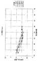
以上のようにして得られた発光位置P(x、0)に応じた光取り出し効率を、図12に示す。これによると、光取り出し効率は、発光位置Pがメサ構造天面の中心点Q(図11に図示)と平面視において対応する活性層の中心点(原点O)から約10μm程度離れた位置では、発光素子にメサ構造が設けられていない場合より低下する。また、発光位置Pが原点Oから10μm以上離れた位置では、発光素子にメサ構造が設けられていない場合とほぼ等しい。このことから、活性層のメサ構造下方からむやみに離れた位置に発光位置Pを設けても、発光素子の輝度が向上しないことが分かる。
【0009】
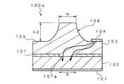
その為、図13に示す発光素子100dのように、前記メサ構造106下方に開口部107aを有する電流狭窄層107を設け、矢印で示すように、通電時に電流狭窄を行うことによって電流密度を高めたものが公知である(例えば、特許文献1を参照)。これにより、この発光素子100dでは、メサ構造106下方の活性層101(発光層)において発光領域Rを限定し、メサ構造106による光取り出し効率の向上を図っている。
【0010】
【発明が解決しようとする課題】
前記発光素子100dにおいて、メサ構造のメサ高さh2および天面幅mの各値に応じた光取り出し効率を求めた。このとき、前記メサ高さh2が4,6,8μmである場合について、また、メサ構造の天面幅mが40,48,56,64,72μmであるときの光取り出し効率を求めた。
【0011】
その結果、図14、図15、図16に示すように、光取り出し効率は、メサ構造のメサ高さh2に比例して高くなることが分かった(特に、発光位置P(x,0)が活性層の中心点(原点O)から約−10〜10μm程度離れた位置において、光取り出し効率が、メサ構造のメサ高さh2に比例して高い)。メサ高さh2を、4μm以上、特に12μm以上にするために、メサ構造106が形成される電流拡散層103の材料にAlGaAsや(AlxGax−1)yIn1−yP(0≦x≦1、0≦y≦1)を用いることが考えられる。このとき、電流拡散層103が格子整合し、歪による劣化が抑制される。しかしながら、それ以外の材料を用いた場合、格子不整合が生じるので、メサ高さh2を制限し、歪による劣化を抑制する必要がある。なお、電流拡散層103が積層されるp−クラッド層102の材料は、発光層101と格子不整合が生じないように選択されている。
【0012】
また、前記グラフから前記メサ構造106の天面幅mを広くしても光取り出し効率が向上しないことが分かった。逆に狭いと発光部の中心部分(発光位置P(x,0)が活性層の中心点(原点O)から約−10〜10μm程度離れた位置)の光取り出し効率は向上するが、発光部の周辺部分の取り出し効率は向上せず、全体としてはむしろ効果が低下する。例えば、発光波長570nmのAlGaInP系発光ダイオードでは、光度30mcdから20mcdに低下した。
【0013】
このように、単純にメサ構造を設けるだけでは光度は向上せず、適切な形状を有するメサ構造を備える半導体発光素子が必要とされていた。
【0014】
そこで、本発明では、前記従来の問題に鑑み、輝度および光取り出し効率を向上させた半導体発光素子を提供することを課題とする。
【0015】
【課題を解決するための手段】
本発明は、前記課題を解決するための手段として、
発光層と、該発光層に積層された電流拡散層と、該電流拡散層表面をエッチングすることにより形成されたメサ構造とを備える半導体発光素子において、
前記メサ構造の天面の見込み半角を、ほぼ全反射角にしたものである。
【0016】
前記発明によれば、メサ構造の天面の見込み半角がほぼ全反射角になっているので、発光層からメサ構造の天面に見込み半角内の角度で入射した光は、メサ構造の天面を介して素子外部に取り出され、発光素子の輝度を向上する。ここで、メサ構造の天面の見込み半角とは、平面においてメサ構造の天面の中心点と対応する発光層の発光位置からメサ構造の天面外縁に入射するときの入射角度のことをいう。
【0017】
前記電流拡散層は、(AlxGax−1)yIn1−yP(0≦x≦1、0≦y≦1)からなり、前記メサ構造の側面の見込み角が、35°以上150°以下であることが好ましい。電流拡散層を(AlxGax−1)yIn1−yP(0≦x≦1、0≦y≦1)で形成した場合、全反射角は約17°となる。このとき、前記メサ構造の天面の見込み半角は、14°〜17°、好ましくは17°である。また、メサ構造の側面の見込み角の上限値を150°にしたのは、メサ構造側面(斜面)と垂直方向との間の角度を41°とした場合、見込み角がおよそ150°となるためである。これにより、メサ構造の天面の見込み半角が全反射角となり、発光した光のうち内部に戻っていた光をメサ構造の側面より外部へと取り出し、発光素子の輝度を向上させることができる。ここで、メサ構造の側面の見込み角とは、平面においてメサ構造の天面の中心点と対応する発光層の発光位置からメサ構造の側面外縁に入射するときの入射角度の2倍の大きさを有する角度のことである。また、電流拡散層が発光層に対して格子整合するので、メサ構造の高さを12μm以上の高さに形成できる。また、短波長の発光素子に適用可能である。
【0018】
また、前記電流拡散層は、AlGaAsからなり、前記メサ構造の側面の見込み角が、35°以上150°以下であることが好ましい。電流拡散層をAlGaAsで形成した場合、全反射角は約17°となる。このとき、前記メサ構造の天面の見込み半角は、17°である。これにより、メサ構造の天面の見込み半角が全反射角となり、発光した光のうち内部に戻っていた光をメサ構造の側面より外部へと取り出し、発光素子の輝度を向上させることができる。また、電流拡散層が発光層に対して格子整合するので、メサ構造の高さを12μm以上の高さに形成できる。
【0019】
前記発光層は、(AlxGax−1)yIn1−yP(0≦x≦1、0≦y≦1)からなることが好ましい。このとき、発光層から発光される光の発光波長は、570nmである。
【0020】
前記メサ構造の高さを4μm以上12μm以下とすることが好ましい。メサ構造の高さを高くして光取り出し効率を向上するためには、メサ構造が形成される電流拡散層の層厚を厚くする必要がある。このとき、電流拡散層が発光層に対して格子不整合となる場合、電流拡散層の層厚を厚くすると歪によりメサ構造を含む電流拡散層に劣化が生じる。このメサ構造の劣化を防止するため、メサ構造の高さを4μm以上12μm以下とする。メサ構造の高さを4μm以上12μm以下とするとき、電流拡散層厚制御を行うことにより達成することが好ましい。
【0021】
前記メサ構造は、前記電流拡散層表面を複数回エッチングすることによりドーム形状に形成されることにより、光取り出し効率が向上する。
【0024】
【発明の実施の形態】
以下、本発明の実施の形態を添付図面に従って説明する。
【0025】
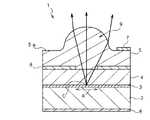
図1は、本発明に係る半導体発光素子1の断面図である。この半導体発光素子1は、基板2、活性層3(発光層)、p−クラッド層4、および電流拡散層5からなる多層構造を有する。基板2の下面に裏面電極6を設け、電流拡散層5の上面にp−電極7を設けたものである。前記活性層3および前記電流拡散層5は、(AlxGax−1)yIn1−yP(0≦x≦1、0≦y≦1)からなる。この発光素子1に通電すると、活性層3が発光するようになっている。また、p−クラッド層4と電流拡散層5との間には、従来の発光素子と同様に、電流狭窄することによって電流密度を高めるための電流狭窄層8が形成されている。
【0026】
また、電流拡散層5の上面5a(素子表面)には、メサ構造9が形成されている。このメサ構造9のメサ高さh2、すなわち電流拡散層5表面からメサ構造9の天面までの高さは4μm以上12μm以下であり、前記メサ構造の天面幅mは3〜9μmである。
【0027】
また、メサ構造9の天面9aの見込み半角r1は、ほぼ全反射角(約17°)になっている。ここで、メサ構造の天面の見込み半角r1とは、平面においてメサ構造9の天面9aの中心点Qと対応する活性層3の発光位置Oからメサ構造9の天面9a外縁に入射するときの入射角度のことをいう。
【0028】
また、メサ構造9の側面9bの見込み角r2は、35°である。ここで、メサ構造の側面の見込み角r2とは、前記発光位置Oからメサ構造9の側面9b外縁に入射するときの入射角度r3の2倍の大きさを有する角度r2のことである。なお、本実施形態においては、メサ構造9の側面9bの見込み角r2は、35°としたが35°以上150°以下であればよい。
【0029】
次に、前記半導体発光素子1を製造する製造方法について説明する。
【0030】
図2(a)に示すように、先ず、基板2上に(AlxGax−1)yIn1−yP(0≦x≦1、0≦y≦1)からなる活性層3、p−クラッド層4、電流狭窄層8および(AlxGax−1)yIn1−yP(0≦x≦1、0≦y≦1)からなる電流拡散層5を順次積層する。ここで、p−クラッド層4上面から電流拡散層5表面までの高さh3は、14μmであり、活性層3上面から電流拡散層5表面までの高さh4は、13μmとなるように積層した。
【0031】
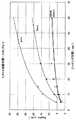
次に、図2(b)に示すように、電流拡散層5上面の一部をレジスト10により保護する。そして、図2(c)に示すように、電流拡散層5をエッチングし、メサ構造9を形成する。このエンチング時に使用するエッチャントは、硫酸系エッチャントでは、60℃で10分間エッチングを行っても約1μm程度しかエッチングできない為、塩酸:酢酸:過水のエッチャントを使用する。その際、エッチャント作成後約15分ほど経過してからエッチングを開始する。これは、図3に示すように、エッチャント作成直後から1時間後のエッチングレートを見ると、エッチングレートが大きく異なり、エッチャント作成直後が最もエッチングレートが速いが、エッチングばらつきが多くなり、逆に、作成後1時間経つとエッチングレートが遅くなり、エッチングするのが困難になるためである。
【0032】
続いて、図2(d)に示すように、レジスト10を剥離した後、スパッタ法或いは蒸着法により電流拡散層5上面に電極材料を薄膜形成し、p−電極7を形成する。さらに、前記基板2の下面に裏面電極6を蒸着する。
【0033】
次に、前記構成からなる半導体発光素子1の作用について説明する。
【0034】
以上のようにして、製造された発光ダイオード1では、図1に示す発光領域Rから発光される光のうち、メサ構造9の天面9aに見込み半角r1以内の角度で入射した光は、見込み半角r1がほぼ全反射角(約17°)であるので天面9aにより反射されることなく外方に射出される。また、発光領域Rから発光される光のうち、メサ構造9の側面9bに入射した光は、メサ構造9の側面9bの見込み角r2が、35°以上であるので、側面9bにより反射されることなく外方に射出される。これにより、光取り出し効率が向上する。また、放出する光の光度を向上することができた。なお、本発明を発光波長570nmのAlGaInP系発光ダイオードに適用した場合、従来の発光素子では30mcdであった光度を58mcdに向上できた。
【0035】
前記実施形態の変形例として、図4に示すように、メサ構造9をドーム形状に形成してもよい。これは、前述した半導体発光素子1を製造する製造方法において、レジスト10剥離後にさらに追加エッチングを行ったものである。これにより、前記実施形態と同様に放出する光の光度を向上することができる。
【0036】
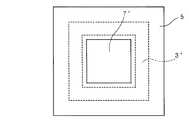
図5(a)は、本発明の他の実施形態に係る半導体発光素子1’の断面図である。この半導体発光素子1’では、図5(b)に示すように、p−電極7’がメサ構造9の天面9aに形成されている。また、環形状の活性層3’(発光層)が、平面視において前記p−電極7’の周囲を囲むように配置されている。また、前記実施形態の電流狭窄層8は、設けられていない。他の前記実施形態と同様である部分は、同一符号を付して詳細な説明は省略する。
【0037】
以上の構成からなる半導体発光素子1’では、p−電極7’の外縁と環形状の活性層3’の外縁との距離が均等であるので、発光領域Rにおいて通電する電流の電流拡散が均一となる。これに対して、図6に示すように、p−電極7’の外縁と活性層3’の外縁との距離が不均等な場合、電流拡散が不均一になり発光領域(特に、活性層3’の角部)の輝度が低下してしまう。また、図7に示すように、環形状の活性層3’を設けるのではなく、p−電極7’の外縁と環形状の活性層3’の外縁との距離が均等になるように多角形状の活性層3’を形成してもよい。
【0038】
【発明の効果】
以上の説明から明らかなように、本発明は、発光層と、該発光層に積層された電流拡散層と、発光層と電流拡散層との間に設けられた電流狭窄層と、電流拡散層表面をエッチングすることにより形成されたメサ構造とを備える半導体発光素子において、電流狭窄層によりメサ構造の天面と対応する位置に発光領域を設け、メサ構造の天面の中心点と対応する発光層の発光位置からメサ構造の天面の外縁に入射するときのメサ構造の天面の見込み半角を、ほぼ全反射角にしたので、発光層からメサ構造の天面に見込み半角内の角度で入射した光は、メサ構造の天面により反射されることなく素子外部に取り出され、発光素子の輝度および光取り出し効率を向上する。
【図面の簡単な説明】
【図1】 本発明の半導体発光素子の断面図である。
【図2】 (a),(b),(c),(d)は、図1の発光ダイオードの製造時を示す断面図である。
【図3】 エッチャント作成後放置時間に応じたエッチングレートを示したグラフである。
【図4】 図1の半導体発光素子の変形例を示す断面図である。
【図5】 (a)は、本発明の他の実施形態に係る半導体発光素子の断面図である。(b)は、(a)の平面図である。
【図6】 p−電極の外縁と活性層の外縁との距離が不均等な場合を示した半導体発光素子の平面図である。
【図7】 図5の変形例を示した平面図である。
【図8】 従来の半導体発光素子の断面図である。
【図9】 従来の半導体発光素子の断面図である。
【図10】 従来の半導体発光素子の断面図である。
【図11】 従来の半導体発光素子の発光素子モデルである。
【図12】 図11の発光素子モデルにおける光取り出し効率を示すグラフである。
【図13】 従来の半導体発光素子の断面図である。
【図14】 図13の半導体発光素子における光取り出し効率を示すグラフである。
【図15】 図13の半導体発光素子における光取り出し効率を示すグラフである。
【図16】 図13の半導体発光素子における光取り出し効率を示すグラフである。
【符号の説明】
1…半導体発光素子
3…活性層(発光層)
5…電流拡散層
9…メサ構造
r1…メサ構造の天面の見込み半角
r2…メサ構造の側面の見込み角[0001]
BACKGROUND OF THE INVENTION
The present invention relates to a semiconductor light emitting device, and more particularly to a light emitting device used for display and communication, particularly a light emitting diode.
[0002]
[Prior art]
Prior art documents related to the present invention include the following.
[0003]
[Patent Document 1]
Japanese Patent No. 2901823 (FIG. 1)
[0004]
As shown in FIG. 8, the conventional light emitting device 100a has a multilayer structure including an active layer 101 (light emitting layer), a p-
[0005]
As shown in FIG. 9, in the other light emitting element 100b, by roughening the
[0006]
In order to solve this problem, a light-emitting element 100c shown in FIG. 10 has a
[0007]
The light extraction efficiency in the light emitting device 100c having the mesa structure will be examined. In the light emitting device model, as shown in FIG. 11, the vertical distance h1 from the upper surface of the active layer to the device surface was 5 μm, and the mesa height h2 from the device surface to the top surface of the mesa structure was 4 μm. The top width m of the mesa structure is 14 μm. The angle t between the mesa structure slope and the vertical direction is 41 °. The light extraction efficiency refers to light emitted at an angle θ with respect to the horizontal direction at the light emission position P (x, 0) on the active layer of the light emitting element model, within the range of the angle θ from 0 to π. It is determined whether or not the light is totally reflected on the element surface every angle θ is 1 °, and is the ratio of the light not totally reflected at this time (however, the multiple reflection in the crystal and the current diffusion layer / air interface) The angle dependence of the transmittance is not considered.) The light extraction efficiency of 1 represents the light extraction efficiency in the case where the light emitting element is not provided with a mesa structure.
[0008]
FIG. 12 shows the light extraction efficiency corresponding to the light emission position P (x, 0) obtained as described above. According to this, the light extraction efficiency is such that the light emission position P is about 10 μm away from the center point Q (shown in FIG. 11) of the top surface of the mesa structure and the center point (origin O) of the active layer corresponding in plan view. This is lower than the case where the light emitting element is not provided with a mesa structure. Further, at a position where the light emitting position P is 10 μm or more away from the origin O, the light emitting element is almost equal to the case where the mesa structure is not provided. From this, it can be seen that the luminance of the light emitting element is not improved even if the light emitting position P is provided at a position distant from the mesa structure below the active layer.
[0009]
Therefore, a
[0010]
[Problems to be solved by the invention]
In the light emitting device 100d, the light extraction efficiency corresponding to each value of the mesa height h2 and the top surface width m of the mesa structure was obtained. At this time, the light extraction efficiency when the mesa height h2 is 4, 6, 8 μm and the top width m of the mesa structure is 40, 48, 56, 64, 72 μm was obtained.
[0011]
As a result, as shown in FIGS. 14, 15, and 16, it was found that the light extraction efficiency increases in proportion to the mesa height h2 of the mesa structure (particularly, the light emission position P (x, 0) is The light extraction efficiency is high in proportion to the mesa height h2 of the mesa structure at a position about −10 to 10 μm away from the center point (the origin O) of the active layer. In order to set the mesa height h2 to 4 μm or more, particularly 12 μm or more, AlGaAs or (Alx Gax-1 )y In1-y P (0 ≦ 0) is used as the material of the
[0012]
Further, it was found from the graph that the light extraction efficiency is not improved even when the top width m of the
[0013]
Thus, simply providing a mesa structure does not improve the luminous intensity, and a semiconductor light emitting device having a mesa structure having an appropriate shape has been required.
[0014]
Therefore, in view of the above-described conventional problems, an object of the present invention is to provide a semiconductor light emitting device with improved luminance and light extraction efficiency.
[0015]
[Means for Solving the Problems]
As a means for solving the above problems, the present invention provides:
In a semiconductor light emitting device comprising a light emitting layer, a current diffusion layer laminated on the light emitting layer, and a mesa structure formed by etching the surface of the current diffusion layer,
The expected half angle of the top surface of the mesa structure is a total reflection angle.
[0016]
According to the invention, since the expected half angle of the top surface of the mesa structure is almost the total reflection angle, the light incident from the light emitting layer to the top surface of the mesa structure at an angle within the expected half angle is the top surface of the mesa structure. Is taken out through the element to improve the luminance of the light emitting element. Here, the expected half angle of the top surface of the mesa structure refers to an incident angle when the light is incident on the outer edge of the top surface of the mesa structure from the light emission position of the light emitting layer corresponding to the center point of the top surface of the mesa structure in a plane. .
[0017]
The current spreading layer is made of (Alx Gax-1 )y In1-y P (0 ≦ x ≦ 1, 0 ≦ y ≦ 1), and a prospective angle of a side surface of the mesa structure is 35 ° or more and 150 It is preferable that the angle is not more than °. When the current spreading layer is formed of (Alx Gax-1 )y In1-y P (0 ≦ x ≦ 1, 0 ≦ y ≦ 1), the total reflection angle is about 17 °. At this time, the expected half angle of the top surface of the mesa structure is 14 ° to 17 °, preferably 17 °. Also, the upper limit of the prospective angle on the side surface of the mesa structure is set to 150 ° because the prospective angle is approximately 150 ° when the angle between the mesa structure side surface (slope) and the vertical direction is 41 °. It is. Thereby, the expected half angle of the top surface of the mesa structure becomes the total reflection angle, and the light that has returned to the inside out of the emitted light is taken out from the side surface of the mesa structure, and the luminance of the light emitting element can be improved. Here, the prospective angle of the side surface of the mesa structure is twice as large as the incident angle when entering the outer edge of the side surface of the mesa structure from the light emitting position of the light emitting layer corresponding to the center point of the top surface of the mesa structure in the plane. It is an angle having Further, since the current diffusion layer is lattice-matched to the light emitting layer, the height of the mesa structure can be formed to a height of 12 μm or more. Moreover, it is applicable to a light emitting element with a short wavelength.
[0018]
The current spreading layer is preferably made of AlGaAs, and the expected angle of the side surface of the mesa structure is preferably 35 ° or more and 150 ° or less. When the current diffusion layer is formed of AlGaAs, the total reflection angle is about 17 °. At this time, the expected half angle of the top surface of the mesa structure is 17 °. Thereby, the expected half angle of the top surface of the mesa structure becomes the total reflection angle, and the light that has returned to the inside out of the emitted light is taken out from the side surface of the mesa structure, and the luminance of the light emitting element can be improved. Further, since the current diffusion layer is lattice-matched to the light emitting layer, the height of the mesa structure can be formed to a height of 12 μm or more.
[0019]
The light emitting layer is preferably made of (Alx Gax-1 )y In1-y P (0 ≦ x ≦ 1, 0 ≦ y ≦ 1). At this time, the emission wavelength of light emitted from the light emitting layer is 570 nm.
[0020]
The height of the mesa structure is preferably 4 μm or more and 12 μm or less. In order to increase the height of the mesa structure and improve the light extraction efficiency, it is necessary to increase the thickness of the current diffusion layer in which the mesa structure is formed. At this time, in the case where the current diffusion layer is lattice mismatched to the light emitting layer, if the thickness of the current diffusion layer is increased, the current diffusion layer including the mesa structure is degraded due to strain. In order to prevent the mesa structure from being deteriorated, the height of the mesa structure is set to 4 μm or more and 12 μm or less. When the height of the mesa structure is 4 μm or more and 12 μm or less, it is preferably achieved by controlling the current diffusion layer thickness.
[0021]
The mesa structure is formed into a dome shape by etching the current diffusion layer surface a plurality of times, thereby improving light extraction efficiency.
[0024]
DETAILED DESCRIPTION OF THE INVENTION
Hereinafter, embodiments of the present invention will be described with reference to the accompanying drawings.
[0025]
FIG. 1 is a cross-sectional view of a semiconductor
[0026]
A
[0027]
Further, the expected half angle r1 of the top surface 9a of the
[0028]
Further, the prospective angle r2 of the side surface 9b of the
[0029]
Next, a manufacturing method for manufacturing the semiconductor
[0030]
As shown in FIG. 2A, first, an
[0031]
Next, as shown in FIG. 2B, a part of the upper surface of the
[0032]
Subsequently, as shown in FIG. 2D, after the resist 10 is peeled off, an electrode material is formed as a thin film on the upper surface of the
[0033]
Next, the operation of the semiconductor
[0034]
In the
[0035]
As a modification of the embodiment, the
[0036]
FIG. 5A is a cross-sectional view of a semiconductor
[0037]
In the semiconductor
[0038]
【The invention's effect】
As is apparent from the above description, the present invention provides a light emitting layer, a current diffusion layer laminated on thelight emitting layer, a current confinement layer provided between thelight emitting layer and the current diffusion layer, and a current diffusion layer. In a semiconductor light emitting device having a mesa structure formed by etching the surface, alight emission region is provided at a position corresponding to the top surface of the mesa structure by thecurrent confinement layer, and light emission corresponding to the center point of the top surface of the mesa structure The expected half angle of the top surface ofthe mesa structurewhen entering the outer edge of the top surface of the mesa structure from the light emitting position of the layer is almost the total reflection angle, so the angle within the expected half angle from the light emitting layer to the top surface of the mesa structure The incident light is extracted outside the element without being reflected by the top surface of the mesa structure, and the luminance and light extraction efficiency of the light emitting element are improved.
[Brief description of the drawings]
FIG. 1 is a cross-sectional view of a semiconductor light emitting device of the present invention.
FIGS. 2A, 2B, 2C, and 2D are cross-sectional views showing the manufacturing time of the light emitting diode of FIG.
FIG. 3 is a graph showing an etching rate according to a standing time after creating an etchant.
4 is a cross-sectional view showing a modification of the semiconductor light emitting device of FIG. 1. FIG.
FIG. 5A is a cross-sectional view of a semiconductor light emitting device according to another embodiment of the present invention. (B) is a top view of (a).
FIG. 6 is a plan view of a semiconductor light emitting device showing a case where the distance between the outer edge of the p-electrode and the outer edge of the active layer is uneven.
7 is a plan view showing a modified example of FIG. 5. FIG.
FIG. 8 is a cross-sectional view of a conventional semiconductor light emitting device.
FIG. 9 is a cross-sectional view of a conventional semiconductor light emitting device.
FIG. 10 is a cross-sectional view of a conventional semiconductor light emitting device.
FIG. 11 is a light emitting element model of a conventional semiconductor light emitting element.
12 is a graph showing light extraction efficiency in the light emitting element model of FIG.
FIG. 13 is a cross-sectional view of a conventional semiconductor light emitting device.
14 is a graph showing light extraction efficiency in the semiconductor light emitting device of FIG.
15 is a graph showing light extraction efficiency in the semiconductor light emitting device of FIG.
16 is a graph showing light extraction efficiency in the semiconductor light emitting device of FIG.
[Explanation of symbols]
DESCRIPTION OF
5 ... Current spreading
Claims (3)
Translated fromJapanese前記電流狭窄層により前記メサ構造の天面と対応する位置に発光領域を設け、
前記メサ構造の天面の中心点と対応する発光層の発光位置から前記メサ構造の天面の外縁に入射するときの前記メサ構造の天面の見込み半角を、ほぼ全反射角にしたことを特徴とする半導体発光素子。A light emitting layer, a current diffusion layer laminated on the lightemitting layer, a current confinement layer provided between the light emitting layer and the current diffusion layer, and a mesa formed by etching the surface of the current diffusion layer. In a semiconductor light emitting device comprising a structure,
A light emitting region is provided at a position corresponding to the top surface of the mesa structure by the current confinement layer,
The expected half angle of the top surface of the mesa structurewhen entering the outer edge of the top surface of the mesa structure from the light emission position of the light emitting layer corresponding to the center point of the top surface of the mesa structure is set to a substantially total reflection angle. A semiconductor light emitting device characterized.
Priority Applications (1)
| Application Number | Priority Date | Filing Date | Title |
|---|---|---|---|
| JP2002325222AJP4093843B2 (en) | 2002-11-08 | 2002-11-08 | Semiconductor light emitting device |
Applications Claiming Priority (1)
| Application Number | Priority Date | Filing Date | Title |
|---|---|---|---|
| JP2002325222AJP4093843B2 (en) | 2002-11-08 | 2002-11-08 | Semiconductor light emitting device |
Publications (2)
| Publication Number | Publication Date |
|---|---|
| JP2004158778A JP2004158778A (en) | 2004-06-03 |
| JP4093843B2true JP4093843B2 (en) | 2008-06-04 |
Family
ID=32804519
Family Applications (1)
| Application Number | Title | Priority Date | Filing Date |
|---|---|---|---|
| JP2002325222AExpired - Fee RelatedJP4093843B2 (en) | 2002-11-08 | 2002-11-08 | Semiconductor light emitting device |
Country Status (1)
| Country | Link |
|---|---|
| JP (1) | JP4093843B2 (en) |
Families Citing this family (3)
| Publication number | Priority date | Publication date | Assignee | Title |
|---|---|---|---|---|
| JP2009016560A (en)* | 2007-07-04 | 2009-01-22 | Sharp Corp | Semiconductor light emitting device |
| JP5324116B2 (en)* | 2008-03-28 | 2013-10-23 | 京セラ株式会社 | Light emitting device and manufacturing method thereof |
| EP4386876A4 (en)* | 2021-08-30 | 2024-12-04 | Sony Group Corporation | LIGHT-EMMITTING DEVICE AND IMAGE DISPLAY DEVICE |
- 2002
- 2002-11-08JPJP2002325222Apatent/JP4093843B2/ennot_activeExpired - Fee Related
Also Published As
| Publication number | Publication date |
|---|---|
| JP2004158778A (en) | 2004-06-03 |
Similar Documents
| Publication | Publication Date | Title |
|---|---|---|
| CN101316026B (en) | Nitride semiconductor laser chip and fabrication method thereof | |
| JP6947386B2 (en) | Semiconductor light emitting element and manufacturing method of semiconductor light emitting element | |
| JP5963004B2 (en) | Nitride semiconductor light emitting device | |
| JP5521478B2 (en) | Nitride semiconductor light emitting device manufacturing method and nitride semiconductor light emitting device | |
| CN1729600B (en) | Semiconductor device with self-aligned semiconductor platform and contact layer and method of manufacturing related device | |
| US10381804B2 (en) | Vertical cavity light emitting element | |
| US20080308833A1 (en) | Group III nitride-based compound semiconductor light-emitting device | |
| US9991418B2 (en) | Semiconductor light emitting element | |
| JP6152848B2 (en) | Semiconductor light emitting device | |
| CN105264676A (en) | LED element and method for producing same | |
| JPWO2018083896A1 (en) | Semiconductor device, semiconductor laser, and manufacturing method of semiconductor device | |
| US11979001B2 (en) | Surface-emitting semiconductor laser | |
| CN109314157B (en) | deep ultraviolet light emitting element | |
| JP2008311317A (en) | Semiconductor light-emitting element | |
| TW201031066A (en) | Semiconductor light-emitting element and method for manufacturing the same | |
| JP2011091251A (en) | Nitride semiconductor light-emitting device | |
| JP2010251531A (en) | Semiconductor light-emitting element | |
| JP4093843B2 (en) | Semiconductor light emitting device | |
| JPH08255952A (en) | Fabrication of semiconductor light emission element | |
| US20070158662A1 (en) | Two-dimensional photonic crystal LED | |
| JP7227469B2 (en) | Vertical cavity surface emitting laser device | |
| JP2004128107A (en) | Optical semiconductor device | |
| JP2011258883A (en) | Semiconductor laser | |
| TW200412698A (en) | Semiconductor laser device | |
| JP2005268725A (en) | Semiconductor device and method for manufacturing the same |
Legal Events
| Date | Code | Title | Description |
|---|---|---|---|
| A621 | Written request for application examination | Free format text:JAPANESE INTERMEDIATE CODE: A621 Effective date:20050525 | |
| A977 | Report on retrieval | Free format text:JAPANESE INTERMEDIATE CODE: A971007 Effective date:20071126 | |
| A131 | Notification of reasons for refusal | Free format text:JAPANESE INTERMEDIATE CODE: A131 Effective date:20071204 | |
| A521 | Written amendment | Free format text:JAPANESE INTERMEDIATE CODE: A523 Effective date:20080129 | |
| TRDD | Decision of grant or rejection written | ||
| A01 | Written decision to grant a patent or to grant a registration (utility model) | Free format text:JAPANESE INTERMEDIATE CODE: A01 Effective date:20080226 | |
| A61 | First payment of annual fees (during grant procedure) | Free format text:JAPANESE INTERMEDIATE CODE: A61 Effective date:20080304 | |
| FPAY | Renewal fee payment (event date is renewal date of database) | Free format text:PAYMENT UNTIL: 20110314 Year of fee payment:3 | |
| R150 | Certificate of patent or registration of utility model | Ref document number:4093843 Country of ref document:JP Free format text:JAPANESE INTERMEDIATE CODE: R150 Free format text:JAPANESE INTERMEDIATE CODE: R150 | |
| FPAY | Renewal fee payment (event date is renewal date of database) | Free format text:PAYMENT UNTIL: 20120314 Year of fee payment:4 | |
| FPAY | Renewal fee payment (event date is renewal date of database) | Free format text:PAYMENT UNTIL: 20120314 Year of fee payment:4 | |
| FPAY | Renewal fee payment (event date is renewal date of database) | Free format text:PAYMENT UNTIL: 20130314 Year of fee payment:5 | |
| FPAY | Renewal fee payment (event date is renewal date of database) | Free format text:PAYMENT UNTIL: 20130314 Year of fee payment:5 | |
| FPAY | Renewal fee payment (event date is renewal date of database) | Free format text:PAYMENT UNTIL: 20140314 Year of fee payment:6 | |
| LAPS | Cancellation because of no payment of annual fees |