JP4092261B2 - Manufacturing method of substrate and manufacturing method of organic electroluminescence element - Google Patents
Manufacturing method of substrate and manufacturing method of organic electroluminescence elementDownload PDFInfo
- Publication number
- JP4092261B2 JP4092261B2JP2003173463AJP2003173463AJP4092261B2JP 4092261 B2JP4092261 B2JP 4092261B2JP 2003173463 AJP2003173463 AJP 2003173463AJP 2003173463 AJP2003173463 AJP 2003173463AJP 4092261 B2JP4092261 B2JP 4092261B2
- Authority
- JP
- Japan
- Prior art keywords
- photoresist coating
- coating film
- substrate
- manufacturing
- photoresist
- Prior art date
- Legal status (The legal status is an assumption and is not a legal conclusion. Google has not performed a legal analysis and makes no representation as to the accuracy of the status listed.)
- Expired - Fee Related
Links
- 239000000758substrateSubstances0.000titleclaimsdescription66
- 238000004519manufacturing processMethods0.000titleclaimsdescription28
- 238000005401electroluminescenceMethods0.000titleclaimsdescription12
- 238000000576coating methodMethods0.000claimsdescription122
- 239000011248coating agentSubstances0.000claimsdescription121
- 229920002120photoresistant polymerPolymers0.000claimsdescription114
- 239000000463materialSubstances0.000claimsdescription42
- 238000000034methodMethods0.000claimsdescription38
- 238000009832plasma treatmentMethods0.000claimsdescription17
- 229920000642polymerPolymers0.000claimsdescription17
- 239000007789gasSubstances0.000claimsdescription15
- 230000008569processEffects0.000claimsdescription14
- 229920001940conductive polymerPolymers0.000claimsdescription13
- CSCPPACGZOOCGX-UHFFFAOYSA-NAcetoneChemical compoundCC(C)=OCSCPPACGZOOCGX-UHFFFAOYSA-N0.000claimsdescription12
- WYURNTSHIVDZCO-UHFFFAOYSA-NTetrahydrofuranChemical compoundC1CCOC1WYURNTSHIVDZCO-UHFFFAOYSA-N0.000claimsdescription12
- QVGXLLKOCUKJST-UHFFFAOYSA-Natomic oxygenChemical compound[O]QVGXLLKOCUKJST-UHFFFAOYSA-N0.000claimsdescription12
- 239000004922lacquerSubstances0.000claimsdescription12
- 239000001301oxygenSubstances0.000claimsdescription12
- 229910052760oxygenInorganic materials0.000claimsdescription12
- 238000004381surface treatmentMethods0.000claimsdescription11
- YCKRFDGAMUMZLT-UHFFFAOYSA-NFluorine atomChemical compound[F]YCKRFDGAMUMZLT-UHFFFAOYSA-N0.000claimsdescription9
- 229910052731fluorineInorganic materials0.000claimsdescription9
- 239000011737fluorineSubstances0.000claimsdescription9
- 229920003986novolacPolymers0.000claimsdescription8
- 239000000203mixtureSubstances0.000claimsdescription7
- 239000004923Acrylic lacquerSubstances0.000claimsdescription6
- 239000004593EpoxySubstances0.000claimsdescription6
- LRHPLDYGYMQRHN-UHFFFAOYSA-NN-ButanolChemical compoundCCCCOLRHPLDYGYMQRHN-UHFFFAOYSA-N0.000claimsdescription6
- 239000004642PolyimideSubstances0.000claimsdescription6
- -1polyethylenePolymers0.000claimsdescription6
- 229920001721polyimidePolymers0.000claimsdescription6
- 230000009467reductionEffects0.000claimsdescription6
- YLQBMQCUIZJEEH-UHFFFAOYSA-NtetrahydrofuranNatural productsC=1C=COC=1YLQBMQCUIZJEEH-UHFFFAOYSA-N0.000claimsdescription6
- LFQSCWFLJHTTHZ-UHFFFAOYSA-NEthanolChemical compoundCCOLFQSCWFLJHTTHZ-UHFFFAOYSA-N0.000claimsdescription5
- 229920000553poly(phenylenevinylene)Polymers0.000claimsdescription5
- TXEYQDLBPFQVAA-UHFFFAOYSA-NtetrafluoromethaneChemical compoundFC(F)(F)FTXEYQDLBPFQVAA-UHFFFAOYSA-N0.000claimsdescription5
- 229920002098polyfluorenePolymers0.000claimsdescription4
- 239000004698PolyethyleneSubstances0.000claimsdescription3
- 229920000172poly(styrenesulfonic acid)Polymers0.000claimsdescription3
- 229920000767polyanilinePolymers0.000claimsdescription3
- 229920000573polyethylenePolymers0.000claimsdescription3
- 229940005642polystyrene sulfonic acidDrugs0.000claimsdescription3
- BDERNNFJNOPAEC-UHFFFAOYSA-Npropan-1-olChemical compoundCCCOBDERNNFJNOPAEC-UHFFFAOYSA-N0.000claimsdescription3
- 239000004094surface-active agentSubstances0.000claimsdescription3
- 239000003960organic solventSubstances0.000claimsdescription2
- 238000007641inkjet printingMethods0.000description9
- 239000000243solutionSubstances0.000description5
- 229920006254polymer filmPolymers0.000description4
- 230000008901benefitEffects0.000description3
- 239000011247coating layerSubstances0.000description3
- 230000007423decreaseEffects0.000description3
- 238000011161developmentMethods0.000description3
- 239000011521glassSubstances0.000description3
- 230000004888barrier functionEffects0.000description2
- AMGQUBHHOARCQH-UHFFFAOYSA-Nindium;oxotinChemical compound[In].[Sn]=OAMGQUBHHOARCQH-UHFFFAOYSA-N0.000description2
- 238000000623plasma-assisted chemical vapour depositionMethods0.000description2
- 239000010703siliconSubstances0.000description2
- 229910052710siliconInorganic materials0.000description2
- 239000002904solventSubstances0.000description2
- 238000004544sputter depositionMethods0.000description2
- 229910052581Si3N4Inorganic materials0.000description1
- VYPSYNLAJGMNEJ-UHFFFAOYSA-NSilicium dioxideChemical compoundO=[Si]=OVYPSYNLAJGMNEJ-UHFFFAOYSA-N0.000description1
- 239000000654additiveSubstances0.000description1
- 230000000996additive effectEffects0.000description1
- 238000013459approachMethods0.000description1
- 239000003637basic solutionSubstances0.000description1
- 230000015572biosynthetic processEffects0.000description1
- 239000003086colorantSubstances0.000description1
- 230000002950deficientEffects0.000description1
- 230000000694effectsEffects0.000description1
- 238000005516engineering processMethods0.000description1
- 238000005530etchingMethods0.000description1
- 238000010438heat treatmentMethods0.000description1
- 229910010272inorganic materialInorganic materials0.000description1
- 239000011147inorganic materialSubstances0.000description1
- 239000002184metalSubstances0.000description1
- 238000012986modificationMethods0.000description1
- 230000004048modificationEffects0.000description1
- 239000011368organic materialSubstances0.000description1
- 239000004033plasticSubstances0.000description1
- 229920003023plasticPolymers0.000description1
- 238000007639printingMethods0.000description1
- 238000012545processingMethods0.000description1
- 239000004065semiconductorSubstances0.000description1
- 238000000926separation methodMethods0.000description1
- 238000004904shorteningMethods0.000description1
- HQVNEWCFYHHQES-UHFFFAOYSA-Nsilicon nitrideChemical compoundN12[Si]34N5[Si]62N3[Si]51N64HQVNEWCFYHHQES-UHFFFAOYSA-N0.000description1
- 229910052814silicon oxideInorganic materials0.000description1
- 238000004528spin coatingMethods0.000description1
- 239000000126substanceSubstances0.000description1
- 229920003051synthetic elastomerPolymers0.000description1
- 239000005061synthetic rubberSubstances0.000description1
- 238000012546transferMethods0.000description1
- 238000001771vacuum depositionMethods0.000description1
- 238000009736wettingMethods0.000description1
Images


Classifications
- G—PHYSICS
- G03—PHOTOGRAPHY; CINEMATOGRAPHY; ANALOGOUS TECHNIQUES USING WAVES OTHER THAN OPTICAL WAVES; ELECTROGRAPHY; HOLOGRAPHY
- G03F—PHOTOMECHANICAL PRODUCTION OF TEXTURED OR PATTERNED SURFACES, e.g. FOR PRINTING, FOR PROCESSING OF SEMICONDUCTOR DEVICES; MATERIALS THEREFOR; ORIGINALS THEREFOR; APPARATUS SPECIALLY ADAPTED THEREFOR
- G03F7/00—Photomechanical, e.g. photolithographic, production of textured or patterned surfaces, e.g. printing surfaces; Materials therefor, e.g. comprising photoresists; Apparatus specially adapted therefor
- G03F7/0035—Multiple processes, e.g. applying a further resist layer on an already in a previously step, processed pattern or textured surface
- G—PHYSICS
- G03—PHOTOGRAPHY; CINEMATOGRAPHY; ANALOGOUS TECHNIQUES USING WAVES OTHER THAN OPTICAL WAVES; ELECTROGRAPHY; HOLOGRAPHY
- G03F—PHOTOMECHANICAL PRODUCTION OF TEXTURED OR PATTERNED SURFACES, e.g. FOR PRINTING, FOR PROCESSING OF SEMICONDUCTOR DEVICES; MATERIALS THEREFOR; ORIGINALS THEREFOR; APPARATUS SPECIALLY ADAPTED THEREFOR
- G03F7/00—Photomechanical, e.g. photolithographic, production of textured or patterned surfaces, e.g. printing surfaces; Materials therefor, e.g. comprising photoresists; Apparatus specially adapted therefor
- G03F7/26—Processing photosensitive materials; Apparatus therefor
- G03F7/40—Treatment after imagewise removal, e.g. baking
- H—ELECTRICITY
- H10—SEMICONDUCTOR DEVICES; ELECTRIC SOLID-STATE DEVICES NOT OTHERWISE PROVIDED FOR
- H10K—ORGANIC ELECTRIC SOLID-STATE DEVICES
- H10K59/00—Integrated devices, or assemblies of multiple devices, comprising at least one organic light-emitting element covered by group H10K50/00
- H10K59/10—OLED displays
- H10K59/12—Active-matrix OLED [AMOLED] displays
- H10K59/122—Pixel-defining structures or layers, e.g. banks
- G—PHYSICS
- G03—PHOTOGRAPHY; CINEMATOGRAPHY; ANALOGOUS TECHNIQUES USING WAVES OTHER THAN OPTICAL WAVES; ELECTROGRAPHY; HOLOGRAPHY
- G03F—PHOTOMECHANICAL PRODUCTION OF TEXTURED OR PATTERNED SURFACES, e.g. FOR PRINTING, FOR PROCESSING OF SEMICONDUCTOR DEVICES; MATERIALS THEREFOR; ORIGINALS THEREFOR; APPARATUS SPECIALLY ADAPTED THEREFOR
- G03F7/00—Photomechanical, e.g. photolithographic, production of textured or patterned surfaces, e.g. printing surfaces; Materials therefor, e.g. comprising photoresists; Apparatus specially adapted therefor
- G03F7/16—Coating processes; Apparatus therefor
- G03F7/168—Finishing the coated layer, e.g. drying, baking, soaking
Landscapes
- Physics & Mathematics (AREA)
- General Physics & Mathematics (AREA)
- Engineering & Computer Science (AREA)
- Microelectronics & Electronic Packaging (AREA)
- Electroluminescent Light Sources (AREA)
Description
Translated fromJapanese【0001】
【発明の属する技術分野】
本発明は、基板及びこれを利用した有機エレクトロルミネッセンス素子に係り、より具体的には安価に製造され、薄いコーティング厚さでも表面エネルギーのコントラストに優れた基板と、これを利用した有機エレクトロルミネッセンス素子に関する。
【0002】
【従来の技術】
インクジェットプリンティング法は、発光ポリマー(Light−Emitting Polymer:LEP)に基づいたフルカラーディスプレーを製造する最も重要な構造形成方法の1つである。この方法によれば、少量のポリマー溶液を適切な基板上に塗布できる。この場合に、空間解像度は基板の表面特性によって決定的に異なる。塗布されたポリマーインクを利用したウェッティングは、カラーミキシングを避けるように、発光ピクセル領域(いわゆる、ピクセル表面)だけに行われるべきである。
【0003】
特許文献1には、基本的な溶液接近方法が記述されている。適切に選択された基板表面形成用材料を利用すれば、基板表面で表面エネルギーのコントラストが形成される。プリント用インクは高表面エネルギー領域だけに流れる一方、低表面エネルギー領域はバリアとして作用する。また、均一なコーティング厚さを有する膜を得るためには、発光ダイオードのピクセル表面の境界領域越に高表面エネルギーを有することが有利である。このように形成された膜は境界領域までは均一に形成され、コーティング厚さはバリア近くの活性領域の外部側で著しく減少する。
【0004】
所望の表面エネルギーのコントラストは種々の方式及び方法によって行われる。
【0005】
特許文献1には、表面の2つのコーティング膜が記述されている。プラズマ表面処理によって、上部コーティング膜が低表面エネルギーを有する一方、下部コーティング膜は同じ処理をする場合、化学的特性によって高表面エネルギーを有する。下部コーティング膜は、一般的に、シリシウムオキシド/ナイトライドのような無機材料を利用して形成される。
【0006】
ここで、無機コーティング膜は高表面エネルギーを有する境界領域に作用し、インクジェットプリンティング法によって均一なポリマー膜が容易に形成できるように作用する。しかし、コーティング作業及び構造の形成過程の際に、半導体産業で一般的に利用される工程を必ず経るべきである。
【0007】
前記コーティングの際に、分離、スパッタリング法及びPECVD(Plasma Enhanced Chemical Vapour Deposition)のようなガス相工程を利用するのが適切である。前記工程は費用がかかり、OLED(Organic Light−Emitting Diode)技術の使用において、費用的なメリットを減少させる。その上、第2コーティング膜は基板表面から所定高さ離れた低表面エネルギー領域(ここでは“セパレーター”)を意味する表面トポロジ
(surface topology)を含む。このような高さプロファイルの結果、前記分離されたポリマー膜は望ましくない厚さプロファイルを形成する。
【0008】
特許文献2では、上部にフォトレジスト膜が予め形成された基板表面を化学的に処理する方法を記述する。その後、前記フォトレジスト膜はマスクを利用して露光及び現像処理する。このように形成された構造物では、フォトレジスト膜が形成された領域は低表面エネルギーを有するのに対し、フォトレジスト膜が形成されていない領域は高表面エネルギーを有する。フォトレジスト膜の側面(flanks)は平均表面エネルギーを有するので、ある程度までは表面エネルギーの突然転移を避けることができる。しかし、この領域が表面エネルギーと形状を自由に調節できる境界領域を表すのではない。インクジェットプリンティング工程の空間解像度は、平均表面エネルギーを有する領域を経て減少する短所を持っている。
【0009】
特許文献3では、表面を2段階処理する方法を開示する。基板面積ははじめに低表面エネルギーを有する。表面の所定領域を短波長光で処理することによって、この領域での表面エネルギーが再び増加する。しかし、この方法では、表面エネルギーのコントラストは制限的で露光時間が長く、大量生産を難しくする。
【0010】
【特許文献1】
EP 0989778 A1(Seiko−Epson)
【特許文献2】
特開平9−203803号公報
【特許文献3】
特開平9−230129公報
【0011】
【発明が解決しようとする課題】
本発明が解決しようとする技術的な課題は、安価に製造でき、従来技術の場合と比較してコーティング厚さが減少し、インクジェットプリンティング用の空間解像度に優れた基板、その製造方法そして前記基板を利用した有機エレクトロルミネッセンス素子及びその製造方法を提供することにある。
【0012】
【課題を解決するための手段】
前記技術的課題のために本発明では、支持基板上に第1フォトレジストコーティング材料を塗布した後、これを露光及び現像する段階と、前記第1フォトレジストコーティング材料を塗布し、露光及び現像した基板を表面処理して高表面エネルギーを有する第1フォトレジストコーティング膜を形成する段階と、前記第1フォトレジストコーティング膜上部の所定領域に第2フォトレジストコーティング材料を塗布して、これを露光及び現像して第2フォトレジストコーティング膜を前記第1フォトレジストコーティング膜上部に部分的に重ねる段階と、前記第2フォトレジストコーティング材料を塗布し、露光及び現像した基板を表面処理して基板の表面エネルギーを減少させる段階と、前記第2フォトレジストコーティング膜を除去する段階とを含むことを特徴とする基板の製造方法を提供する。
【0013】
前記技術的な課題を解決するために、前記第1フォトレジストコーティング膜はUV−オゾン処理または酸素プラズマ処理によって高表面エネルギーを有する。前記表面エネルギーの減少は、フッ素含有ガスを利用したプラズマ処理によって行われ、前記フッ素含有ガスがCF4、SF6及びNF3よりなる群から選択されたいずれか1つ以上である。
【0014】
前記表面エネルギーの減少は、4:1混合体積比のテトラフルオロメタンと酸素よりなる混合ガスを用いたプラズマ処理によって行われる。
【0015】
前記第1フォトレジストコーティング材料及び前記第2フォトレジストコーティング材料は、各々ノボラック系フォトレジスト、アクリルラッカー、エポキシラッカー及びポリイミドラッカーよりなる群から選択されたいずれか1つ以上である。
【0016】
前記第2フォトレジストコーティング膜の除去の際に、アセトン及びテトラヒドロフランよりなる群から選択されたいずれか1つ以上を利用する。
【0022】
他の技術的課題のために本発明ではまた、支持基板上に第1フォトレジストコーティング材料を塗布した後、これを露光及び現像する段階と、前記第1フォトレジストコーティング材料を塗布し、露光及び現像した基板を表面処理して高表面エネルギーを有する第1フォトレジストコーティング膜を形成する段階と、前記第1フォトレジストコーティング膜の上部の所定領域に第2フォトレジストコーティング材料を塗布し、これを露光及び現像して第2フォトレジストコーティング膜を前記第1フォトレジストコーティング膜の上部に部分的に重ねる段階と、前記第2フォトレジストコーティング材料を塗布し、露光及び現像した基板を表面処理して基板の表面エネルギーを減少させる段階と、前記第2フォトレジストコーティング膜を除去する段階と、前記前記第2フォトレジストコーティング膜を除去した基板上に有機膜形成材料を含むインク滴を供給して有機膜を形成する段階とを含む有機エレクトロルミネッセンス素子の製造方法を提供する。
【0023】
前記有機膜形成材料は伝導性ポリマー及び発光ポリマーよりなる群から選択されたいずれか1つ以上である。そして、前記伝導性ポリマーはポリエチレンジオキソチオフェン−ポリスチレンスルホン酸(PEDT−PSS)及びポリアニリンの中から選択されたいずれか1つ以上である。
【0024】
前記伝導性ポリマーの表面張力は界面活性剤及び低級アルコールよりなる群から選択されたいずれか1つ以上によって減少される。ここで、低級アルコールはブタノール及びプロパノールよりなる群から選択されたいずれか1つ以上を使用する。
【0025】
前記有機膜は特に発光部である。
【0027】
【発明の実施の形態】
以下、添付した図面に基づき、本発明を詳細に説明する。
【0028】
本発明のメリットは、商業的に入手可能な材料を使用しつつ、製造コストを低減する方法を使用し、ランダムな構造の表面コントラストを有する1つのコーティング膜だけが形成された基板を提供することにある。
【0029】
前記目的を達成するために、支持基板上に第1フォトレジストコーティング材料を塗布して、第1フォトレジストコーティング膜を形成する。前記第1フォトレジストコーティング材料は商業的に入手可能な材料であり、具体例として、ノボラック系フォトレジスト、アクリルラッカー、エポキシラッカーまたはポリイミドラッカーが挙げられる。次いで、前記塗布された結果物を、フォトマスクを利用して露光及び現像した後、熱的に架橋し、UV−オゾン処理または酸素プラズマ処理のような表面処理を施すことによって、第1フォトレジストコーティング膜は高表面エネルギーを有するようになる。
【0030】
その後、例えば商業的に入手可能なフォトレジストを利用して、第2フォトレジストコーティング膜を形成する。次いで、フォトマスクを利用した露光を再び実施した後、現像処理する。この場合に、第2フォトレジストコーティング膜は第1フォトレジストコーティング膜の上部に部分的に重なる。その後、基板の表面エネルギーは、例えばCF4、SF6またはNF3のようなフッ素ガスを利用した表面処理によって減少する。
【0031】
また、4:1混合体積比の4フッ化メタンと酸素の混合ガスを利用したプラズマ処理によって、表面エネルギーが減少する。最終的に、第2フォトレジストコーティング膜は除去される。第2フォトレジストコーティング膜の除去の際に、アセトン、テトラヒドロフラン、その混合物のような有機溶媒を利用する。残留する第1フォトレジストコーティング膜は、フォトマスクと表面処理法を適切に選択して、所定形状と、所定表面エネルギーのコントラストとを有し得る。
【0032】
さらに他のメリットは、必須の基板特性を得るために、最終的に1つのコーティング膜だけが必要であって、コーティング膜の形成の際に、有機材料だけが使われることにある。このような方法によれば、薄いコーティング厚さでも表面エネルギーのコントラストに優れている。
【0033】
支持基板はガラス、プラスチック、シリシウムまたはその他の軟質または硬質材料よりなる。前記コーティング膜はフォトレジストよりなり、フォトマスクを利用して露光及び現像される。この場合、フォトレジストとして、商業的に入手可能なフォトレジストが利用される。また、同じ方法によって、フォトマスクを利用したエッチングを実施してポリマー膜の構造が形成できる。表面エネルギーは、UV−オゾンまたは酸素プラズマ処理によって低減できる。
【0034】
本発明の基板は、有機エレクトロルミネッセンス素子の有機膜形成の際に利用できる。この際に、有機膜の形成材料が特に制限されることはないが、伝導性ポリマー、発光材料(特に発光ポリマー)、その混合物が例示される。さらに詳細に説明すれば、本発明の基板は、伝導性ポリマーのインプリンティング及び/またはインクジェットプリンティングシステムを利用した発光ポリマー溶液のインプリンティングに利用できる。
【0035】
前記伝導性ポリマーは、ポリエチレンジオキソチオフェン−ポリスチレンスルホン酸(PEDT−PSS)、ポリアニリン及びその混合物よりなる。前記伝導性ポリマーの表面張力は、界面活性剤などの添加剤またはブタノール、プロパノールなどの低級アルコールを利用して低減できる。このような方式で分離されたポリマーコーティング膜は熱処理によって乾燥する。
【0036】
前記発光ポリマーとしては、ポリフェニレンビニレン(PPV)、ポリフルオレン及びその混合物を使用する。
【0037】
後述するインクジェットプリンティング工程において、第1段階は、伝導性ポリマーを含有する溶液のインプリンティング過程である。一方、伝導性ポリマーのコーティング膜は欠陥電子(正孔)を発光材料に注入する能力を向上させるために役立つ。
【0038】
一方、前記コーティング膜はまたアノードコーティング膜(インジウム−スズ−オキシド)を平坦化させてアノードコーティング膜の不規則に基づくOLED寿命の短縮を防止する。
【0039】
最後に、ポリフェニレンビニレン(PPV)及びポリフルオレン(PFO)の中から選択されたいずれか1つ以上の発光ポリマー溶液は、インクジェットプリンティング法でインプリントされる。その後、金属カソードコーティング膜を真空蒸着/スパッタリングによって形成し、最後にカプセル化する。
【0040】
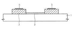
図1に示されるように、ガラス、シリシウムまたは他の材料よりなる硬質または軟質の支持基板1は表面処理の前に利用可能である。後ほど、発光ポリマー(LEP)は所定領域、すなわち活性ピクセル表面2上にインプリンティングされる。
【0041】
一方、相異なるカラーのポリマーの混合(いわゆるカラー混合)を防ぐために、他方では、画像図解のためにポリマーを各々活性化させるために、ポリマーを所定領域に正確に塗布することが要求される。
【0042】
第1フォトレジストコーティング材料を支持基板1上にスピンコーティングした後、フォトマスクを利用した露光処理を経て、基板1上にフォトレジストコーティング膜が形成される。このような過程後、UV−オゾン及び/または酸素−プラズマ処理だけでなく、現像及び熱的後処理過程を経る。このように処理された基板は図2に図示されている。UV−オゾン及び/または酸素−プラズマ処理によって、高表面エネルギーを有する第1フォトレジストコーティング膜3を形成する。
【0043】
その後、図3に示されるように、第2フォトレジストコーティング材料をスピンコーティング法によって塗布する。次いで、フォトマスクを利用して露光及び現像を実施して、第2フォトレジストコーティング膜4を形成する。第2フォトレジストコーティング膜4は第1フォトレジストコーティング膜3の境界領域で重なる。その後、前記支持基板1はフッ素含有ガスを利用したプラズマで処理する。特に、前記フッ素ガスとしてはCF4、SF6またはNF3が適当である。その結果、前記第2フォトレジストコーティング膜4によってカバーされていない第1フォトレジストコーティング膜3の特定領域は、低表面エネルギーを有するようになる。しかし、第2フォトレジストコーティング膜4によって重なった第1フォトレジストコーティング膜3の一部は、比較的高表面エネルギーを有する。
【0044】
その後、第2フォトレジストコーティング膜4は、例えばアセトン、テトラヒドロフラン、その混合物のような適切な溶媒によって除去される。このようにして得られた基板の表面は図4に示される通りである。
【0045】
図4には、高表面エネルギーを有する領域、すなわち、前記第1フォトレジストコーティング膜3の特定領域と、低表面エネルギーを有する領域5を有する部分的なフォトレジストコーティング膜が図示されている。このような領域での形状はフォトマスクの適切な選択によってランダムに配列される。また、高表面エネルギーを有する領域3の表面エネルギーと低表面エネルギーを有する領域5の表面エネルギーの比率は、UV−オゾン及び/または酸素−プラズマ処理によって有利に調節できる。
【0046】
図5は、フォトレジストコーティング膜の上部に位置する、例えば発光半導体性ポリマー(LEP)よりなるインク滴6で処理されたフォトレジストコーティング膜を図示する。インク滴6は、活性ピクセル表面2の領域と高表面エネルギーを有するフォトレジストコーティング膜3の境界領域に流れ込む。
【0047】
活性ピクセル表面2の外部に、表面エネルギーが高い状態から低い状態に移るにつれて、活性ピクセル表面2上でコーティング厚さが均一に確保される。その理由は、コーティング厚の減少が低表面エネルギー領域5だけで起こるので、活性ピクセル表面2の境界領域でのコーティング厚の減少が起こらないためである。このような方式で、均一なパターンを有するポリマー膜が確保される。
【0048】
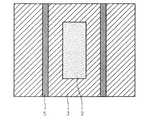
図6は、インクジェットプリンティング後、有機発光要素用基板を示す平面図である。ここで、活性ピクセル表面2と高表面エネルギーとを有するフォトレジスト領域3はインクで濡れる。これと対照的に、低表面エネルギーを有するフォトレジスト領域5はインクによって濡れない。
【0049】
【実施例】
以下、本発明の望ましい実施例について記述することにする。
【0050】
支持基板として、予め形成されたインジウム−スズ−オキシドコーティング膜を有するガラスが利用される。第1フォトレジストコーティング材料のノボラック系フォトレジスト(例えば、Messrs JRS(Japan Synthetic Rubber)の商品名 JEM 750)を厚さ500nmにスピンコーティングした後、適切なフォトマスクを利用して露光させる。露光処理後、前記結果物を200℃で1時間熱処理する。
【0051】
次いで、前記熱処理された結果物を酸素プラズマを利用して120秒間処理し、第1フォトレジストコーティング膜を形成する。その後、第2フォトレジストコーティング材料をスピンコーティングする。この際に、前記第2フォトレジストコーティング材料としては、ノボラック系フォトレジスト(例えば、Messrs Clariantの商品名AZ6612)を利用する。前記第2フォトレジストコーティング材料を適切なフォトマスクを利用して露光処理した後、現像する。
【0052】
基板に、4:1混合体積比の4フッ化メタンと酸素の混合ガスを利用してプラズマ処理を120秒間実施する。その直後、第2フォトレジストコーティング膜をアセトン、テトラヒドロフラン、その混合物のような適切な溶媒によって除去する。
【0053】
基板に、酸素プラズマ処理で簡単な後処理を実施する。このような実施例のためには、セパレーター領域5の幅は約10〜20μmである。ピクセル2の中間空間は約30μmであって、これは約130PPIの分解能に当たる。高表面エネルギーを有する領域の表面エネルギーは約60−70dyne/cmであり、低表面エネルギーを有する領域の表面エネルギーは約20−35dyne/cmである。
【0054】
【発明の効果】
以上述べたように、本発明によれば、本発明の基板は、安価に製造可能で、従来技術の場合と比較してコーティング厚が減少するだけではなく、薄いコーティング厚でも表面エネルギーのコントラストに優れている。かかる基板は伝導性ポリマーのインプリンティングに利用、及び/またはインクジェットプリンティング法を利用した発光ポリマー溶液のインプリント時に使われる。
【0055】
本発明について前記実施例を参考して説明しているが、これは例示的なことに過ぎず、本発明に属する技術分野の当業者ならばこれより多様な変形及び均等な他の実施例が可能であることが理解できるであろう。したがって、本発明の真の技術的な保護範囲は特許請求の範囲の技術的思想により定められるべきである。
【図面の簡単な説明】
【図1】非処理基板表面を示す図面である。
【図2】第1フォトレジストコーティング膜が形成された基板表面を示す。
【図3】第1フォトレジストコーティング膜及び第2フォトレジストコーティング膜、部分的に重なったフォトレジストコーティング膜を有する基板表面を示す図面である(前記各コーティング膜は露光及び現像されている)。
【図4】表面エネルギーの減少処理過程及び第2フォトレジストコーティング膜の除去過程を経た後の基板表面を示す図面である。
【図5】表面処理された基板とインク滴を示す図面である。
【図6】予め供給されたインク滴を有する有機エレクトロルミネッセンス素子用基板の平面図である。
【符号の説明】
1…軟質支持基板
2…ピクセル表面
3…第1フォトレジストコーティング膜
5…低表面エネルギー領域[0001]
BACKGROUND OF THE INVENTION
The present invention relates to a substrate and an organic electroluminescence device using the same, more specifically, a substrate manufactured at low cost and excellent in surface energy contrast even with a thin coating thickness, and an organic electroluminescence device using the same About.
[0002]
[Prior art]
The ink jet printing method is one of the most important structure forming methods for producing a full color display based on a light-emitting polymer (LEP). According to this method, a small amount of polymer solution can be applied on a suitable substrate. In this case, the spatial resolution depends on the surface characteristics of the substrate. Wetting using the applied polymer ink should be performed only on the light emitting pixel areas (so-called pixel surfaces) to avoid color mixing.
[0003]
[0004]
The desired surface energy contrast can be achieved by various methods and methods.
[0005]
[0006]
Here, the inorganic coating film acts on the boundary region having high surface energy, and acts so that a uniform polymer film can be easily formed by the ink jet printing method. However, the process generally used in the semiconductor industry should be performed during the coating process and the structure forming process.
[0007]
In the coating, it is appropriate to use a gas phase process such as separation, sputtering, and PECVD (Plasma Enhanced Chemical Vapor Deposition). The process is expensive and reduces the cost advantage in using OLED (Organic Light-Emitting Diode) technology. In addition, the second coating film includes a surface topology that means a low surface energy region (here, “separator”) that is a predetermined height away from the substrate surface. As a result of such a height profile, the separated polymer film forms an undesirable thickness profile.
[0008]
[0009]
[0010]
[Patent Document 1]
EP 0987778 A1 (Seiko-Epson)
[Patent Document 2]
JP-A-9-203803 [Patent Document 3]
Japanese Patent Laid-Open No. 9-230129
[Problems to be solved by the invention]
A technical problem to be solved by the present invention is a substrate that can be manufactured at a low cost, has a coating thickness reduced as compared with the prior art, and has excellent spatial resolution for inkjet printing, a method for manufacturing the substrate, and the substrate It is an object to provide an organic electroluminescence device utilizing the above and a manufacturing method thereof.
[0012]
[Means for Solving the Problems]
In order to solve the above technical problem, in the present invention, a first photoresist coating material is applied on a support substrate, and then exposed and developed, and the first photoresist coating material is applied, exposed and developed. Forming a first photoresist coating film having a high surface energy by surface-treating the substrate; and applying a second photoresist coating material to a predetermined region on the first photoresist coating film; Developing and partially overlaying the second photoresist coating film on the first photoresist coating film; applying the second photoresist coating material; treating the exposed and developed substrate with a surface treatment; Reducing energy and removing the second photoresist coating layer; To provide a method of manufacturing a substrate, which comprises a floor.
[0013]
In order to solve the technical problem, the first photoresist coating layer has a high surface energy by UV-ozone treatment or oxygen plasma treatment. The reduction of the surface energy is performed by plasma treatment using a fluorine-containing gas, and the fluorine-containing gas is any one or more selected from the group consisting of CF4 , SF6 and NF3 .
[0014]
The reduction of the surface energy is performed by plasma treatment using a mixed gas composed of tetrafluoromethane and oxygen in a 4: 1 mixed volume ratio.
[0015]
Each of the first photoresist coating material and the second photoresist coating material is at least one selected from the group consisting of a novolak photoresist, an acrylic lacquer, an epoxy lacquer, and a polyimide lacquer.
[0016]
At the time of removing the second photoresist coating film, any one or more selected from the group consisting of acetone and tetrahydrofuran is used.
[0022]
For another technical problem, the present invention also provides a step of applying a first photoresist coating material on a support substrate, and then exposing and developing the first photoresist coating material; applying the first photoresist coating material; A surface treatment is performed on the developed substrate to form a first photoresist coating film having a high surface energy, and a second photoresist coating material is applied to a predetermined region on the first photoresist coating film. Exposing and developing a second photoresist coating film partially overlying the first photoresist coating film; applying the second photoresist coating material; and subjecting the exposed and developed substrate to a surface treatment. Reducing the surface energy of the substrate and removing the second photoresist coating layer; The method comprising, providing a method of manufacturing an organic electroluminescent device comprising forming an organic film by supplying an ink droplet containing an organic film-forming material on a substrate obtained by removing the second photoresist coating film.
[0023]
The organic film forming material is at least one selected from the group consisting of a conductive polymer and a light emitting polymer. The conductive polymer is at least one selected from polyethylene dioxothiophene-polystyrene sulfonic acid (PEDT-PSS) and polyaniline.
[0024]
The surface tension of the conductive polymer is reduced by any one or more selected from the group consisting of a surfactant and a lower alcohol. Here, the lower alcohol is any one or more selected from the group consisting of butanol and propanol.
[0025]
The organic film is particularly a light emitting part.
[0027]
DETAILED DESCRIPTION OF THE INVENTION
Hereinafter, the present invention will be described in detail with reference to the accompanying drawings.
[0028]
An advantage of the present invention is to provide a substrate on which only one coating film having a surface contrast of a random structure is formed using a method that reduces manufacturing costs while using commercially available materials. It is in.
[0029]
To achieve the above object, a first photoresist coating material is applied on a support substrate to form a first photoresist coating film. The first photoresist coating material is a commercially available material, and specific examples include novolak photoresist, acrylic lacquer, epoxy lacquer, and polyimide lacquer. Next, the coated result is exposed and developed using a photomask, thermally crosslinked, and subjected to a surface treatment such as UV-ozone treatment or oxygen plasma treatment to thereby form a first photoresist. The coating film has a high surface energy.
[0030]
Thereafter, a second photoresist coating film is formed using, for example, a commercially available photoresist. Next, after performing exposure using a photomask again, development processing is performed. In this case, the second photoresist coating film partially overlaps the upper portion of the first photoresist coating film. Thereafter, the surface energy of the substrate is reduced by a surface treatment using a fluorine gas such as CF4 , SF6 or NF3 .
[0031]
Further, the surface energy is reduced by the plasma treatment using a mixed gas of tetrafluoromethane and oxygen having a 4: 1 mixed volume ratio. Finally, the second photoresist coating film is removed. In removing the second photoresist coating film, an organic solvent such as acetone, tetrahydrofuran, or a mixture thereof is used. The remaining first photoresist coating film may have a predetermined shape and a predetermined surface energy contrast by appropriately selecting a photomask and a surface treatment method.
[0032]
Yet another advantage is that only one coating film is ultimately required to obtain the required substrate properties, and only organic materials are used in forming the coating film. According to such a method, the surface energy contrast is excellent even with a thin coating thickness.
[0033]
The support substrate is made of glass, plastic, silicon, or other soft or hard material. The coating film is made of a photoresist, and is exposed and developed using a photomask. In this case, a commercially available photoresist is used as the photoresist. Further, the structure of the polymer film can be formed by performing etching using a photomask by the same method. The surface energy can be reduced by UV-ozone or oxygen plasma treatment.
[0034]
The board | substrate of this invention can be utilized in the case of organic film formation of an organic electroluminescent element. At this time, the material for forming the organic film is not particularly limited, and examples thereof include conductive polymers, light emitting materials (particularly light emitting polymers), and mixtures thereof. More specifically, the substrate of the present invention can be used for imprinting conductive polymers and / or imprinting light emitting polymer solutions using an inkjet printing system.
[0035]
The conductive polymer is composed of polyethylene dioxothiophene-polystyrene sulfonic acid (PEDT-PSS), polyaniline, and a mixture thereof. The surface tension of the conductive polymer can be reduced by using an additive such as a surfactant or a lower alcohol such as butanol or propanol. The polymer coating film separated in this manner is dried by heat treatment.
[0036]
As the light emitting polymer, polyphenylene vinylene (PPV), polyfluorene and a mixture thereof are used.
[0037]
In the inkjet printing process described later, the first stage is an imprinting process of a solution containing a conductive polymer. On the other hand, the coating film of the conductive polymer is useful for improving the ability to inject defective electrons (holes) into the light emitting material.
[0038]
Meanwhile, the coating film also planarizes the anode coating film (indium-tin-oxide) to prevent shortening of the OLED lifetime due to irregularities of the anode coating film.
[0039]
Finally, any one or more light-emitting polymer solutions selected from polyphenylene vinylene (PPV) and polyfluorene (PFO) are imprinted by an inkjet printing method. Thereafter, a metal cathode coating film is formed by vacuum deposition / sputtering and finally encapsulated.
[0040]
As shown in FIG. 1, a hard or
[0041]
On the other hand, in order to prevent mixing of polymers of different colors (so-called color mixing), on the other hand, in order to activate each polymer for image illustration, it is required to accurately apply the polymer to a predetermined area.
[0042]
After the first photoresist coating material is spin-coated on the
[0043]
Thereafter, as shown in FIG. 3, a second photoresist coating material is applied by spin coating. Next, exposure and development are performed using a photomask to form a second
[0044]
Thereafter, the second
[0045]
FIG. 4 shows a partial photoresist coating film having a region having a high surface energy, that is, a specific region of the first
[0046]
FIG. 5 illustrates a photoresist coating film that has been treated with ink droplets 6 made of, for example, a light emitting semiconducting polymer (LEP), located on top of the photoresist coating film. The ink droplet 6 flows into the boundary area between the area of the
[0047]
As the surface energy moves from a high state to a low state outside the
[0048]
FIG. 6 is a plan view showing the organic light emitting element substrate after inkjet printing. Here, the
[0049]
【Example】
Hereinafter, preferred embodiments of the present invention will be described.
[0050]
As the support substrate, a glass having a preformed indium-tin-oxide coating film is used. A first novolac-based photoresist (for example, trade name JEM 750 of Messrs JRS (Japan Synthetic Rubber)) is spin-coated to a thickness of 500 nm, and then exposed using an appropriate photomask. After the exposure process, the resultant is heat-treated at 200 ° C. for 1 hour.
[0051]
Next, the heat-treated result is processed using oxygen plasma for 120 seconds to form a first photoresist coating film. Thereafter, a second photoresist coating material is spin coated. At this time, as the second photoresist coating material, a novolak photoresist (for example, trade name AZ6612 of Messrs Clariant) is used. The second photoresist coating material is exposed using an appropriate photomask and then developed.
[0052]
Plasma treatment is performed on the substrate for 120 seconds using a mixed gas of tetrafluoromethane and oxygen in a 4: 1 mixed volume ratio. Immediately thereafter, the second photoresist coating film is removed with a suitable solvent such as acetone, tetrahydrofuran, or a mixture thereof.
[0053]
The substrate is subjected to simple post-treatment by oxygen plasma treatment. For such an embodiment, the width of the
[0054]
【The invention's effect】
As described above, according to the present invention, the substrate of the present invention can be manufactured at low cost, and not only the coating thickness is reduced as compared with the case of the prior art, but also the surface energy contrast is reduced even with a thin coating thickness. Are better. Such a substrate is used for imprinting a conductive polymer and / or used for imprinting a light-emitting polymer solution using an inkjet printing method.
[0055]
Although the present invention has been described with reference to the above-described embodiments, this is merely illustrative, and various modifications and equivalent other embodiments may be made by those skilled in the art to which the present invention pertains. It will be understood that this is possible. Therefore, the true technical protection scope of the present invention should be determined by the technical idea of the claims.
[Brief description of the drawings]
FIG. 1 is a drawing showing a surface of a non-processed substrate.
FIG. 2 shows a substrate surface on which a first photoresist coating film is formed.
FIG. 3 is a view illustrating a substrate surface having a first photoresist coating film, a second photoresist coating film, and a partially overlapping photoresist coating film (the coating films are exposed and developed);
FIG. 4 is a view illustrating a substrate surface after a process of reducing surface energy and a process of removing a second photoresist coating film.
FIG. 5 is a view showing a surface-treated substrate and ink droplets.
FIG. 6 is a plan view of an organic electroluminescence element substrate having ink droplets supplied in advance.
[Explanation of symbols]
DESCRIPTION OF
Claims (22)
Translated fromJapanese前記第1フォトレジストコーティング材料を塗布し、露光及び現像した基板を表面処理して高表面エネルギーを有する第1フォトレジストコーティング膜を形成する段階と、
前記第1フォトレジストコーティング膜の上部の所定領域に第2フォトレジストコーティング材料を塗布し、これを露光及び現像して第2フォトレジストコーティング膜を前記第1フォトレジストコーティング膜の上部に部分的に重ねる段階と、
前記第2フォトレジストコーティング材料を塗布し、露光及び現像した基板を表面処理して基板の表面エネルギーを減少させる段階と、
前記第2フォトレジストコーティング膜を除去する段階と、を含むことを特徴とする基板の製造方法。After applying a first photoresist coating material on a support substrate, exposing and developing it;
Applying the first photoresist coating material, surface-treating the exposed and developed substrate to form a first photoresist coating film having high surface energy;
A second photoresist coating material is applied to a predetermined region on the first photoresist coating film, and the second photoresist coating film is exposed and developed to partially apply the second photoresist coating film on the first photoresist coating film. Layering,
Applying the second photoresist coating material, surface treating the exposed and developed substrate to reduce the surface energy of the substrate;
Removing the second photoresist coating film. A method for manufacturing a substrate, comprising:
フッ素含有ガスを利用したプラズマ処理によって行われることを特徴とする請求項1または2に記載の基板の製造方法。The reduction in surface energy is
The method for producing a substrate according to claim 1 or 2, wherein the substrate treatment is performed by plasma treatment using a fluorine-containing gas.
4:1混合体積比のテトラフルオロメタンと酸素よりなる混合ガスとを利用したプラズマ処理によって行われることを特徴とする請求項1に記載の基板の製造方法。The reduction in surface energy is
2. The method of manufacturing a substrate according to claim 1, wherein the substrate is formed by plasma treatment using a mixed gas composed of tetrafluoromethane and oxygen in a 4: 1 mixed volume ratio.
前記第1フォトレジストコーティング材料を塗布し、露光及び現像した基板を表面処理して高表面エネルギーを有する第1フォトレジストコーティング膜を形成する段階と、
前記第1フォトレジストコーティング膜の上部の所定領域に第2フォトレジストコーティング材料を塗布し、これを露光及び現像して第2フォトレジストコーティング膜を前記第1フォトレジストコーティング膜の上部に部分的に重ねる段階と、
前記第2フォトレジストコーティング材料を塗布し、露光及び現像した基板を表面処理して基板の表面エネルギーを減少させる段階と、
前記第2フォトレジストコーティング膜を除去する段階と、
前記第2フォトレジストコーティング膜を除去した基板上に有機膜形成材料を含むインク滴を供給して有機膜を形成する段階と、を含む有機エレクトロルミネッセンス素子の製造方法。After applying a first photoresist coating material on a support substrate, exposing and developing it;
Applying the first photoresist coating material, surface-treating the exposed and developed substrate to form a first photoresist coating film having high surface energy;
A second photoresist coating material is applied to a predetermined region on the first photoresist coating film, and the second photoresist coating film is exposed and developed to partially apply the second photoresist coating film on the first photoresist coating film. Layering,
Applying the second photoresist coating material, surface treating the exposed and developed substrate to reduce the surface energy of the substrate;
Removing the second photoresist coating film;
Forming an organic film by supplying ink droplets containing an organic film-forming material on the substrate from which the second photoresist coating film has been removed, and a method for producing an organic electroluminescent device.
フッ素含有ガスを利用したプラズマ処理によって行われることを特徴とする請求項9に記載の有機エレクトロルミネッセンス素子の製造方法。A reduction in surface energy of the first photoresist coating film or the second photoresist coating film,
The method for producing an organic electroluminescent element according to claim9 , wherein the process is performed by plasma treatment using a fluorine-containing gas.
4:1混合体積比のテトラフルオロメタンと酸素よりなる混合ガスを利用したプラズマ処理によって行われることを特徴とする請求項9に記載の有機エレクトロルミネッセンス素子の製造方法。The reduction in surface energy is
The method for producing an organic electroluminescent device according to claim9 , wherein the method is performed by plasma treatment using a mixed gas composed of tetrafluoromethane and oxygen in a 4: 1 mixed volume ratio.
Applications Claiming Priority (2)
| Application Number | Priority Date | Filing Date | Title |
|---|---|---|---|
| DE10236404ADE10236404B4 (en) | 2002-08-02 | 2002-08-02 | Process for producing a substrate |
| KR10-2003-0015598AKR100528256B1 (en) | 2002-08-02 | 2003-03-13 | Substrate and organic electroluminescence device using the substrate |
Publications (2)
| Publication Number | Publication Date |
|---|---|
| JP2004071547A JP2004071547A (en) | 2004-03-04 |
| JP4092261B2true JP4092261B2 (en) | 2008-05-28 |
Family
ID=32031464
Family Applications (1)
| Application Number | Title | Priority Date | Filing Date |
|---|---|---|---|
| JP2003173463AExpired - Fee RelatedJP4092261B2 (en) | 2002-08-02 | 2003-06-18 | Manufacturing method of substrate and manufacturing method of organic electroluminescence element |
Country Status (3)
| Country | Link |
|---|---|
| US (1) | US7015501B2 (en) |
| JP (1) | JP4092261B2 (en) |
| CN (1) | CN100492714C (en) |
Families Citing this family (34)
| Publication number | Priority date | Publication date | Assignee | Title |
|---|---|---|---|---|
| JP2005079560A (en)* | 2003-09-04 | 2005-03-24 | Hitachi Ltd | Thin film transistor, display device, and manufacturing method thereof |
| US20050153114A1 (en)* | 2004-01-14 | 2005-07-14 | Rahul Gupta | Printing of organic electronic devices |
| US20050282308A1 (en)* | 2004-06-22 | 2005-12-22 | Albrecht Uhlig | Organic electroluminescent display device and method of producing the same |
| KR100615229B1 (en)* | 2004-06-29 | 2006-08-25 | 삼성에스디아이 주식회사 | Thin film transistors, flat panel display devices including the thin film transistors, and methods of manufacturing the thin film transistors |
| KR100579186B1 (en)* | 2004-10-15 | 2006-05-11 | 삼성에스디아이 주식회사 | Organic electroluminescent element |
| KR20070103402A (en)* | 2004-12-30 | 2007-10-23 | 이 아이 듀폰 디 네모아 앤드 캄파니 | Containment Structures and Methods |
| KR100639919B1 (en)* | 2005-10-10 | 2006-11-01 | 한국전자통신연구원 | Surface treatment method of fiber reinforced plastic substrate |
| WO2007049631A1 (en)* | 2005-10-28 | 2007-05-03 | Nissan Chemical Industries, Ltd. | Charge-transporting varnish for spray or inkjet application |
| WO2007106101A2 (en)* | 2006-03-02 | 2007-09-20 | E. I. Du Pont De Nemours And Company | Process for making contained layers and devices made with same |
| US8124172B2 (en)* | 2006-03-02 | 2012-02-28 | E.I. Du Pont De Nemours And Company | Process for making contained layers and devices made with same |
| US8309376B2 (en)* | 2007-10-26 | 2012-11-13 | E I Du Pont De Nemours And Company | Process and materials for making contained layers and devices made with same |
| EP2109163A1 (en)* | 2008-04-08 | 2009-10-14 | Alcan Technology & Management Ltd. | Substrate with printed structure |
| KR101002667B1 (en) | 2008-07-02 | 2010-12-21 | 삼성모바일디스플레이주식회사 | Thin film transistor, manufacturing method thereof and organic light emitting display device comprising same |
| KR101041141B1 (en) | 2009-03-03 | 2011-06-13 | 삼성모바일디스플레이주식회사 | Organic light emitting display device and manufacturing method |
| KR101015849B1 (en)* | 2009-03-03 | 2011-02-23 | 삼성모바일디스플레이주식회사 | Thin film transistor, manufacturing method thereof and organic light emitting display device comprising same |
| KR101049799B1 (en)* | 2009-03-03 | 2011-07-15 | 삼성모바일디스플레이주식회사 | Thin film transistor, manufacturing method thereof and organic light emitting display device comprising same |
| KR101049801B1 (en) | 2009-03-05 | 2011-07-15 | 삼성모바일디스플레이주식회사 | Method for manufacturing polycrystalline silicon layer and atomic layer deposition apparatus used therein |
| KR20100100187A (en)* | 2009-03-05 | 2010-09-15 | 삼성모바일디스플레이주식회사 | Fabrication method of polycrystalline silicon |
| KR101056428B1 (en)* | 2009-03-27 | 2011-08-11 | 삼성모바일디스플레이주식회사 | Thin film transistor, manufacturing method thereof, and organic light emitting display device comprising the same |
| EP2459379A4 (en)* | 2009-07-27 | 2015-05-06 | Du Pont | PROCESS AND MATERIALS FOR MANUFACTURING DELIMITED LAYERS AND DEVICES MADE THEREBY |
| KR101094295B1 (en)* | 2009-11-13 | 2011-12-19 | 삼성모바일디스플레이주식회사 | Manufacturing method of polycrystalline silicon layer, manufacturing method of thin film transistor, and manufacturing method of organic light emitting display device |
| US9935289B2 (en) | 2010-09-10 | 2018-04-03 | Industrial Technology Research Institute Institute | Environmental sensitive element package and encapsulation method thereof |
| CN102466966B (en)* | 2010-11-10 | 2014-04-02 | 中国科学院微电子研究所 | Method for improving electron beam exposure efficiency |
| KR101854133B1 (en)* | 2011-10-28 | 2018-06-15 | 삼성디스플레이 주식회사 | Method of forming an organic light emitting structure and method of manufacturing an organic light emitting display device |
| CN103241025B (en)* | 2013-04-28 | 2015-02-04 | 京东方科技集团股份有限公司 | Ink jet printing method of organic thin film |
| CN103367391B (en)* | 2013-06-28 | 2016-03-23 | 京东方科技集团股份有限公司 | Pixel defines the manufacture method of layer |
| US10333066B2 (en) | 2013-06-28 | 2019-06-25 | Boe Technology Group Co., Ltd. | Pixel definition layer and manufacturing method thereof, display substrate and display device |
| CN103346123B (en)* | 2013-06-28 | 2015-07-01 | 京东方科技集团股份有限公司 | Pixel defining layer, manufacturing method thereof, display substrate and display device |
| CN104464956B (en)* | 2014-12-03 | 2017-02-01 | 中国科学院化学研究所 | High-precision and interval-controllable electrode and preparing method thereof |
| CN104681592B (en)* | 2014-12-23 | 2018-01-19 | 上海天马有机发光显示技术有限公司 | A kind of display panel and preparation method thereof and display device |
| US9847509B2 (en) | 2015-01-22 | 2017-12-19 | Industrial Technology Research Institute | Package of flexible environmental sensitive electronic device and sealing member |
| CN105428553B (en)* | 2015-11-11 | 2018-09-18 | 广东聚华印刷显示技术有限公司 | A kind of printed form display device and preparation method thereof |
| US10243175B2 (en) | 2016-02-02 | 2019-03-26 | Samsung Display Co., Ltd. | Organic light-emitting apparatus fabricated using a fluoropolymer and method of manufacturing the same |
| CN111063816A (en)* | 2019-12-19 | 2020-04-24 | 深圳市华星光电半导体显示技术有限公司 | Organic light-emitting diode, preparation method and display device |
Family Cites Families (6)
| Publication number | Priority date | Publication date | Assignee | Title |
|---|---|---|---|---|
| US4856043A (en)* | 1988-07-18 | 1989-08-08 | North American Philips Corporation | Two piece ceramic Soller slit collimator for X-ray collimation |
| US5373544A (en)* | 1992-08-12 | 1994-12-13 | Siemens Aktiengesellschaft | X-ray diffractometer |
| US20030148024A1 (en)* | 2001-10-05 | 2003-08-07 | Kodas Toivo T. | Low viscosity precursor compositons and methods for the depositon of conductive electronic features |
| JP2001043980A (en)* | 1999-07-29 | 2001-02-16 | Sony Corp | Organic electroluminescence element and display device |
| EP1411088B1 (en)* | 2001-07-26 | 2013-08-21 | Nissan Chemical Industries, Ltd. | Polyamic acid resin composition |
| US6908861B2 (en)* | 2002-07-11 | 2005-06-21 | Molecular Imprints, Inc. | Method for imprint lithography using an electric field |
- 2003
- 2003-06-18JPJP2003173463Apatent/JP4092261B2/ennot_activeExpired - Fee Related
- 2003-07-28USUS10/627,683patent/US7015501B2/ennot_activeExpired - Lifetime
- 2003-08-01CNCNB031586759Apatent/CN100492714C/ennot_activeExpired - Lifetime
Also Published As
| Publication number | Publication date |
|---|---|
| CN1496198A (en) | 2004-05-12 |
| CN100492714C (en) | 2009-05-27 |
| US7015501B2 (en) | 2006-03-21 |
| JP2004071547A (en) | 2004-03-04 |
| US20040079940A1 (en) | 2004-04-29 |
Similar Documents
| Publication | Publication Date | Title |
|---|---|---|
| JP4092261B2 (en) | Manufacturing method of substrate and manufacturing method of organic electroluminescence element | |
| CN1653628B (en) | Method of preparation of organic optoelectronic and electronic devices and devices thereby obtained | |
| KR100577903B1 (en) | Thin film patterning substrate and its surface treatment | |
| CN100435601C (en) | Manufacturing method of organic electroluminescent element, organic electroluminescent element | |
| US7737631B2 (en) | Flat panel display with repellant and border areas and method of manufacturing the same | |
| CN105932037B (en) | A kind of organic electroluminescent display substrate and preparation method thereof, display device | |
| US7833612B2 (en) | Substrate for inkjet printing and method of manufacturing the same | |
| US9006715B2 (en) | Electronic device | |
| CN109449314B (en) | Display substrate, method for manufacturing the same, and display panel | |
| KR20130035920A (en) | Method for manufacturing organic light-emitting device | |
| JP2010153381A (en) | Organic light emitting display device, and method of manufacturing the same | |
| CN108198845B (en) | Pixel definition layer and preparation method, display substrate and preparation method, display device | |
| KR100528256B1 (en) | Substrate and organic electroluminescence device using the substrate | |
| CN100385704C (en) | Fabrication method of structured electrode | |
| TW200541385A (en) | Printing of organic electronic devices | |
| CN1873999B (en) | Flat panel display and method of manufacturing the same | |
| US20090057657A1 (en) | Method for forming pattern arrays and organic devices including the pattern arrays | |
| US8168377B2 (en) | Pattern forming method and method of manufacturing semiconductor device by using the same | |
| US20050282308A1 (en) | Organic electroluminescent display device and method of producing the same | |
| KR100875653B1 (en) | Method of forming fine pattern of semiconductor device | |
| KR20030075971A (en) | Method for fabricating thin film pattern for organic electronic devices | |
| JP4283139B2 (en) | Organic EL display device substrate and manufacturing method thereof, and organic EL display device and manufacturing method thereof | |
| KR100657534B1 (en) | An organic electro luminescent display device and a method for producing the same | |
| CN116234396A (en) | Light emitting device and manufacturing method thereof | |
| Ji et al. | 73‐3: Distinguished Student Paper: Full Color Quantum Dot Light‐Emitting Diodes Patterned by Photolithography Technology |
Legal Events
| Date | Code | Title | Description |
|---|---|---|---|
| A621 | Written request for application examination | Free format text:JAPANESE INTERMEDIATE CODE: A621 Effective date:20040713 | |
| A131 | Notification of reasons for refusal | Free format text:JAPANESE INTERMEDIATE CODE: A131 Effective date:20070904 | |
| A521 | Request for written amendment filed | Free format text:JAPANESE INTERMEDIATE CODE: A523 Effective date:20071127 | |
| TRDD | Decision of grant or rejection written | ||
| A01 | Written decision to grant a patent or to grant a registration (utility model) | Free format text:JAPANESE INTERMEDIATE CODE: A01 Effective date:20080205 | |
| A61 | First payment of annual fees (during grant procedure) | Free format text:JAPANESE INTERMEDIATE CODE: A61 Effective date:20080303 | |
| R150 | Certificate of patent or registration of utility model | Ref document number:4092261 Country of ref document:JP Free format text:JAPANESE INTERMEDIATE CODE: R150 Free format text:JAPANESE INTERMEDIATE CODE: R150 | |
| FPAY | Renewal fee payment (event date is renewal date of database) | Free format text:PAYMENT UNTIL: 20110307 Year of fee payment:3 | |
| FPAY | Renewal fee payment (event date is renewal date of database) | Free format text:PAYMENT UNTIL: 20110307 Year of fee payment:3 | |
| S111 | Request for change of ownership or part of ownership | Free format text:JAPANESE INTERMEDIATE CODE: R313111 | |
| FPAY | Renewal fee payment (event date is renewal date of database) | Free format text:PAYMENT UNTIL: 20110307 Year of fee payment:3 | |
| R371 | Transfer withdrawn | Free format text:JAPANESE INTERMEDIATE CODE: R371 | |
| FPAY | Renewal fee payment (event date is renewal date of database) | Free format text:PAYMENT UNTIL: 20110307 Year of fee payment:3 | |
| S111 | Request for change of ownership or part of ownership | Free format text:JAPANESE INTERMEDIATE CODE: R313111 | |
| FPAY | Renewal fee payment (event date is renewal date of database) | Free format text:PAYMENT UNTIL: 20110307 Year of fee payment:3 | |
| R360 | Written notification for declining of transfer of rights | Free format text:JAPANESE INTERMEDIATE CODE: R360 | |
| FPAY | Renewal fee payment (event date is renewal date of database) | Free format text:PAYMENT UNTIL: 20110307 Year of fee payment:3 | |
| FPAY | Renewal fee payment (event date is renewal date of database) | Free format text:PAYMENT UNTIL: 20110307 Year of fee payment:3 | |
| R350 | Written notification of registration of transfer | Free format text:JAPANESE INTERMEDIATE CODE: R350 | |
| FPAY | Renewal fee payment (event date is renewal date of database) | Free format text:PAYMENT UNTIL: 20110307 Year of fee payment:3 | |
| R250 | Receipt of annual fees | Free format text:JAPANESE INTERMEDIATE CODE: R250 | |
| FPAY | Renewal fee payment (event date is renewal date of database) | Free format text:PAYMENT UNTIL: 20120307 Year of fee payment:4 | |
| FPAY | Renewal fee payment (event date is renewal date of database) | Free format text:PAYMENT UNTIL: 20130307 Year of fee payment:5 | |
| R250 | Receipt of annual fees | Free format text:JAPANESE INTERMEDIATE CODE: R250 | |
| FPAY | Renewal fee payment (event date is renewal date of database) | Free format text:PAYMENT UNTIL: 20130307 Year of fee payment:5 | |
| S111 | Request for change of ownership or part of ownership | Free format text:JAPANESE INTERMEDIATE CODE: R313111 | |
| S531 | Written request for registration of change of domicile | Free format text:JAPANESE INTERMEDIATE CODE: R313531 | |
| FPAY | Renewal fee payment (event date is renewal date of database) | Free format text:PAYMENT UNTIL: 20130307 Year of fee payment:5 | |
| R371 | Transfer withdrawn | Free format text:JAPANESE INTERMEDIATE CODE: R371 | |
| S111 | Request for change of ownership or part of ownership | Free format text:JAPANESE INTERMEDIATE CODE: R313111 | |
| S531 | Written request for registration of change of domicile | Free format text:JAPANESE INTERMEDIATE CODE: R313531 | |
| FPAY | Renewal fee payment (event date is renewal date of database) | Free format text:PAYMENT UNTIL: 20130307 Year of fee payment:5 | |
| R350 | Written notification of registration of transfer | Free format text:JAPANESE INTERMEDIATE CODE: R350 | |
| FPAY | Renewal fee payment (event date is renewal date of database) | Free format text:PAYMENT UNTIL: 20140307 Year of fee payment:6 | |
| R250 | Receipt of annual fees | Free format text:JAPANESE INTERMEDIATE CODE: R250 | |
| R250 | Receipt of annual fees | Free format text:JAPANESE INTERMEDIATE CODE: R250 | |
| R250 | Receipt of annual fees | Free format text:JAPANESE INTERMEDIATE CODE: R250 | |
| R250 | Receipt of annual fees | Free format text:JAPANESE INTERMEDIATE CODE: R250 | |
| R250 | Receipt of annual fees | Free format text:JAPANESE INTERMEDIATE CODE: R250 | |
| R250 | Receipt of annual fees | Free format text:JAPANESE INTERMEDIATE CODE: R250 | |
| R250 | Receipt of annual fees | Free format text:JAPANESE INTERMEDIATE CODE: R250 | |
| R250 | Receipt of annual fees | Free format text:JAPANESE INTERMEDIATE CODE: R250 | |
| R250 | Receipt of annual fees | Free format text:JAPANESE INTERMEDIATE CODE: R250 | |
| R250 | Receipt of annual fees | Free format text:JAPANESE INTERMEDIATE CODE: R250 | |
| LAPS | Cancellation because of no payment of annual fees |