JP4087949B2 - Electro-optical device manufacturing method and electro-optical device - Google Patents
Electro-optical device manufacturing method and electro-optical deviceDownload PDFInfo
- Publication number
- JP4087949B2 JP4087949B2JP13890698AJP13890698AJP4087949B2JP 4087949 B2JP4087949 B2JP 4087949B2JP 13890698 AJP13890698 AJP 13890698AJP 13890698 AJP13890698 AJP 13890698AJP 4087949 B2JP4087949 B2JP 4087949B2
- Authority
- JP
- Japan
- Prior art keywords
- electro
- pixel
- optical device
- driving circuit
- pitch
- Prior art date
- Legal status (The legal status is an assumption and is not a legal conclusion. Google has not performed a legal analysis and makes no representation as to the accuracy of the status listed.)
- Expired - Fee Related
Links
- 238000004519manufacturing processMethods0.000titleclaimsdescription46
- 239000000758substrateSubstances0.000claimsdescription72
- 239000010409thin filmSubstances0.000claimsdescription30
- 238000000034methodMethods0.000claimsdescription27
- 229920002120photoresistant polymerPolymers0.000claimsdescription20
- 230000015572biosynthetic processEffects0.000claimsdescription17
- 238000006243chemical reactionMethods0.000claimsdescription8
- 239000011159matrix materialSubstances0.000claimsdescription8
- 238000000059patterningMethods0.000claimsdescription2
- 239000004973liquid crystal related substanceSubstances0.000description44
- 239000011521glassSubstances0.000description21
- 239000010408filmSubstances0.000description17
- 239000003990capacitorSubstances0.000description11
- 238000010586diagramMethods0.000description9
- 230000002093peripheral effectEffects0.000description8
- 239000004065semiconductorSubstances0.000description7
- 229910052751metalInorganic materials0.000description6
- 239000002184metalSubstances0.000description6
- 239000003566sealing materialSubstances0.000description5
- 102100025393Succinate dehydrogenase cytochrome b560 subunit, mitochondrialHuman genes0.000description4
- 101710142922Succinate dehydrogenase cytochrome b560 subunit, mitochondrialProteins0.000description4
- 230000000694effectsEffects0.000description4
- 229910021420polycrystalline siliconInorganic materials0.000description4
- 229920005591polysiliconPolymers0.000description4
- 238000013461designMethods0.000description3
- 102100028183Cytohesin-interacting proteinHuman genes0.000description2
- 101000916686Homo sapiens Cytohesin-interacting proteinProteins0.000description2
- 238000005229chemical vapour depositionMethods0.000description2
- 230000007423decreaseEffects0.000description2
- 238000005516engineering processMethods0.000description2
- VYPSYNLAJGMNEJ-UHFFFAOYSA-Nsilicon dioxideInorganic materialsO=[Si]=OVYPSYNLAJGMNEJ-UHFFFAOYSA-N0.000description2
- 238000012546transferMethods0.000description2
- VYZAMTAEIAYCRO-UHFFFAOYSA-NChromiumChemical compound[Cr]VYZAMTAEIAYCRO-UHFFFAOYSA-N0.000description1
- XUIMIQQOPSSXEZ-UHFFFAOYSA-NSiliconChemical compound[Si]XUIMIQQOPSSXEZ-UHFFFAOYSA-N0.000description1
- BQCADISMDOOEFD-UHFFFAOYSA-NSilverChemical compound[Ag]BQCADISMDOOEFD-UHFFFAOYSA-N0.000description1
- CDBYLPFSWZWCQE-UHFFFAOYSA-LSodium CarbonateChemical compound[Na+].[Na+].[O-]C([O-])=OCDBYLPFSWZWCQE-UHFFFAOYSA-L0.000description1
- 230000015556catabolic processEffects0.000description1
- 229910052804chromiumInorganic materials0.000description1
- 239000011651chromiumSubstances0.000description1
- 239000004020conductorSubstances0.000description1
- 238000001312dry etchingMethods0.000description1
- 238000005530etchingMethods0.000description1
- 238000003384imaging methodMethods0.000description1
- 238000003780insertionMethods0.000description1
- 230000037431insertionEffects0.000description1
- 239000011229interlayerSubstances0.000description1
- 239000000463materialSubstances0.000description1
- 230000003287optical effectEffects0.000description1
- 239000010453quartzSubstances0.000description1
- 239000000565sealantSubstances0.000description1
- 229910052710siliconInorganic materials0.000description1
- 239000010703siliconSubstances0.000description1
- 229910052709silverInorganic materials0.000description1
- 239000004332silverSubstances0.000description1
- 239000002356single layerSubstances0.000description1
- 238000012360testing methodMethods0.000description1
- 238000001039wet etchingMethods0.000description1
Images


Classifications
- G—PHYSICS
- G02—OPTICS
- G02F—OPTICAL DEVICES OR ARRANGEMENTS FOR THE CONTROL OF LIGHT BY MODIFICATION OF THE OPTICAL PROPERTIES OF THE MEDIA OF THE ELEMENTS INVOLVED THEREIN; NON-LINEAR OPTICS; FREQUENCY-CHANGING OF LIGHT; OPTICAL LOGIC ELEMENTS; OPTICAL ANALOGUE/DIGITAL CONVERTERS
- G02F1/00—Devices or arrangements for the control of the intensity, colour, phase, polarisation or direction of light arriving from an independent light source, e.g. switching, gating or modulating; Non-linear optics
- G02F1/01—Devices or arrangements for the control of the intensity, colour, phase, polarisation or direction of light arriving from an independent light source, e.g. switching, gating or modulating; Non-linear optics for the control of the intensity, phase, polarisation or colour
- G02F1/13—Devices or arrangements for the control of the intensity, colour, phase, polarisation or direction of light arriving from an independent light source, e.g. switching, gating or modulating; Non-linear optics for the control of the intensity, phase, polarisation or colour based on liquid crystals, e.g. single liquid crystal display cells
- G02F1/133—Constructional arrangements; Operation of liquid crystal cells; Circuit arrangements
- G02F1/136—Liquid crystal cells structurally associated with a semi-conducting layer or substrate, e.g. cells forming part of an integrated circuit
- G02F1/1362—Active matrix addressed cells
- G02F1/13625—Patterning using multi-mask exposure
Landscapes
- Liquid Crystal (AREA)
Description
Translated fromJapanese【0001】
【発明の属する技術分野】
本発明は、液晶パネル等の電気光学装置を製造する製造方法及び該電気光学装置の技術分野に属し、特に、投影露光装置(以下、適宜“ステッパー”と称す)を用いて大型且つ高詳細なドライバ内蔵型(画素部とドライバ回路とが同一基板に作り込まれている)のアクティブマトリクス駆動方式の液晶パネル等の電気光学装置を製造するのに好適な電気光学装置の製造方法の技術分野及びこのように製造される電気光学装置の技術分野に属する。
【0002】
【従来の技術】
大規模集積回路(LSI)等の半導体装置を製造する方法の技術分野では、一枚の大型ウエーハ上に同一構成の半導体装置をマトリクス状に多数製造する技術が一般的である。この製造中に、半導体膜、金属膜等の各種薄膜をパターニングするためにフォトレジストをマスクを介して露光する露光工程が行われるが、大量生産の際には、微細化及び量産に適した縮小投影露光が通常行われる。即ち、ステッパーと呼ばれる縮小投影露光装置により、拡大寸法のマスク(レチクル)の縮小像をウエーハ上に投影結像し、1チップ〜数チップ分の露光を同時に行い、ウエーハをステップ移動しながら、この露光を繰り返して行うことによりウエーハ全面を露光する。
【0003】
従来、多数の薄膜トランジスタ(以下、適宜“TFT”と称す)を含んで構成されるドライバ内蔵型のTFTアクティブマトリクス駆動方式の液晶パネル等の電気光学装置を製造する場合にも、液晶パネル等が対角1インチ程度の小型なものであれば、上述の半導体装置を製造する場合と同様に、ステッパーによる1回の露光によりマザー基板上において1個以上の液晶パネル等を構成することになる基板部分を同時に露光できる。従って、半導体装置の場合と同様に微細化を図ることができ、また、1枚の大型のマザー基板から複数の液晶パネル等の大量生産を効率良く行うこともできる。この場合には特に、ドライバ部を構成する各駆動回路セル(即ち、駆動回路における信号線を駆動する一単位)に至る配線長さや画面表示領域の各画素部に至る配線長さの差により、各駆動回路セルから出力される駆動電圧の差が発生しないように、更に画面表示領域の周囲の狭い領域にドライバ部がコンパクトに収まるように、画面表示領域における画素ピッチとドライバ部における駆動回路セルのピッチとは同一とされる。そして、画面表示領域に配列された複数の信号線各々の一端には、該信号線を駆動するための駆動回路セルが規則正しく接続される。
【0004】
このようなステッパーによる投影露光は、投影するために、余り大きな領域を同時に露光する目的には適さない。即ち、同時に露光する領域を大きくするに連れて、露光のスループットが低下し、露光領域内の各点における結像状態や位置合わせも困難となり、露光精度も低下してしまう。このため、実践上は例えば対角10インチ程度の大型の基板上に画素部とドライバ回路とを有する液晶パネル等を製造する際にステッパーを用いることはない。
【0005】
他方で、ステッパーを用いた一技術として、大型回路を製造する場合には、1回の露光で大型回路となる領域の一部のみを露光し、複数回の露光により一つの大型回路となる全領域を露光する技術がある。この技術では特に、別々に露光される領域間の境界(以下、“露光境界”と称す)において、配線や素子等が寸断されないように配慮する必要がある。このため露光境界では、両方の露光領域を重ねる(即ち、2重露光する)ことにより、配線や素子等の継目部分を形成するようにしている。なお、このような大型回路の場合には縮小投影だけでなく、等倍投影も用いられることが多い。
【0006】
従って、この技術を利用して液晶パネルを製造する場合にも、当該液晶パネルが大型であってもドライバ内蔵型でなければ、上述のステッパーを用いた技術により、配線等について緩いデザインルールの下で、多くの継目部分を含むようにしつつ当該液晶パネルを製造できる。即ち、液晶パネルの基板上に複雑な素子を含む周辺回路(ドライバ部)を形成する必要が無いため、継目部分が多少存在しても或いはデザインルールが緩くても、後に外付けドライバ回路をTAB(テープ・オートメイテッド・ボンディング)等により接続すれば、ステッパーを用いて実践上問題の少ない大型の液晶パネルを製造できる。
【0007】
【発明が解決しようとする課題】
しかしながら、ドライバ内蔵型の液晶パネル等の電気光学装置の場合には、基板上における画面表示領域の周囲に複雑な回路素子を多数含んで構成されるドライバ部を形成する必要があるため、液晶パネルを大型化すると、前述のステッパーを用いての製造が困難となってしまう。けだし、ステッパーを用いた1回の露光により、大型の液晶パネルを1つ構成する基板部分に対応する領域全体を露光できないため、前述の如き継目部分が複数存在せざるをえないが、このような継目部分を含むように、多数の複雑な駆動回路を構成することは実際上困難だからである。特に、アナログ信号を扱うTFT、抵抗、容量等の回路素子を含む比較的複雑な駆動回路を作成する場合、継目部分における薄膜部分のバラツキがこれらの回路素子の特性のバラツキとなるため、敢えて、このような大型のドライバ内蔵型の液晶パネルを単純にステッパーを用いて製造すれば、極めて性能の不安定な或いは信頼性に欠けるものとなってしまうという問題点がある。
【0008】
他方で、ステッパーを使用することなく、大型のドライバ内蔵型の液晶パネル等をアライナー等を使用して1回の露光により製造する場合には、例えば、数μm程度が微細化の実践的な意味での限界となってしまい、ステッパーを用いて比較的低コストで実現可能な1μm程度或いはそれ以下の微細化を行うことができない。従って、TFT等の素子や配線などの微細化により、素子の高速化、配線の低容量化、低消費電力化、高解像度化、装置全体の小型薄型化などを図ることができないという問題点がある。
【0009】
本発明は上述した問題点に鑑みなされたものであり、駆動回路を内蔵すると共に高性能且つ大型の電気光学装置をステッパーを使用して製造可能である電気光学装置の製造方法及びこの方法により製造される電気光学装置を提供することを課題とする。
【0010】
【課題を解決するための手段】
本発明の電気光学装置の製造方法は上記課題を解決するために、基板上に、第1方向及び該第1方向に交わる第2方向にマトリクス状に配列されてなる複数の画素部からなる画面表示領域と、該複数の画素部の前記第2方向の配列に対応して前記画面表示領域の周囲に夫々設けられており前記複数の画素部を駆動するための複数の第1方向駆動回路セルとを備えた電気光学装置を製造する電気光学装置の製造方法であって、前記基板上にパターニングされる薄膜を形成する薄膜形成工程と、該薄膜上にフォトレジストを形成するフォトレジスト形成工程と、該フォトレジストが形成された領域を少なくとも前記第1方向に複数分割してなる所定ブロック領域毎に、前記複数の画素部が前記第1方向に所定第1ピッチを持つように且つ前記複数の第1方向駆動回路セルが前記第1方向に前記所定第1ピッチよりも小さい所定第2ピッチを持つように所定パターンのマスクを介して露光用光源により投影露光する投影露光工程と、該投影露光工程により一のブロック領域を露光した後に他のブロック領域を露光すべく前記基板を前記露光用光源に対して相対的に順次移動させる移動工程と、該露光されたフォトレジストを用いて前記薄膜をパターニングすることにより前記複数の画素部及び前記複数の第1方向駆動回路セルを夫々構成する複数の素子を少なくとも部分的に形成する素子形成工程とを含み、前記投影露光工程及び移動工程において、前記画面表示領域内外の境界に、前記複数の画素部と前記複数の第1方向駆動回路セルとを相互に夫々接続する複数の配線を含む配線ピッチ変換部を形成するように露光及び移動し、前記素子形成工程において、前記配線ピッチ変換部を更に形成することを特徴とする。
【0011】
上記本発明によれば、先ず、薄膜形成工程において、基板上にパターニングされる薄膜が形成され、フォトレジスト形成工程において、該薄膜上にフォトレジストが形成される。ここで、投影露光工程においては、露光領域は、少なくとも第1方向に複数分割されてなる所定ブロック領域に予め分割される。そして、このブロック領域毎に、複数の画素部が第1方向に所定第1ピッチを持つように且つ複数の第1方向駆動回路セルが第1方向に所定第1ピッチよりも小さい所定第2ピッチを持つように、所定パターンのマスクを介して露光用光源による投影露光が行われる。ここで、投影露光工程により一のブロック領域が露光される度に、移動工程により、露光用光源に対して基板が相対的に順次移動され、他のブロック領域が繰り返し露光される。そして、素子形成工程において、エッチング等により、露光されたフォトレジストを用いて薄膜がパターニングされ、複数の画素部及び複数の第1方向駆動回路セルを夫々構成する複数の素子は、少なくとも部分的に形成される。
【0012】
従って、複数の第1方向駆動回路セルは、各ブロック領域において画素ピッチたる第1ピッチよりも小さい第2ピッチで形成されるため、第1方向駆動回路セルを構成するTFT、容量、抵抗器等の回路素子を、ブロック領域の境界、即ち露光境界を跨るように形成しなくても配置することができる。この結果、継目部分における薄膜部分のバラツキがこれらの回路素子の特性のバラツキとなって現われる事態を未然に防止でき、性能が安定しており信頼性の高い第1方向駆動回路セルを形成できる。また、本発明のかかる構成によれば、画面表示領域内外の境界に、複数の画素部と複数の第1方向駆動回路セルとを相互に夫々接続する複数の配線を含む配線ピッチ変換部が形成される。従って、画素ピッチと第1方向駆動回路セルのピッチとが相異なっていても、両者間の電気的接続を配線ピッチ変換部によりとることができる。
【0013】
これに加えて、ブロック領域毎に露光を行うので、例えば、対角10インチやそれ以上の大型の電気光学装置であっても、ステッパーを用いて当該投影露光を行うことが可能となる。よって、TFT等の素子や配線などの微細化により、素子の高速化、配線の低容量化、低消費電力化、高解像度化、装置全体の小型薄型化などを図ることができる。
【0014】
以上の結果、本発明によれば、ステッパー技術を利用して、複数の第1方向駆動回路セルから構成される駆動回路を内蔵すると共に高性能且つ大型の電気光学装置を比較的効率良く且つ低コストで製造できる。
【0021】
本発明の電気光学装置の製造方法は、さらに、前記複数の画素部の前記第1方向の配列に対応して前記画面表示領域の周囲に夫々設けられており、前記基板上には前記複数の画素部を駆動するための複数の第2方向駆動回路セルを更に備えており、前記投影露光工程において、前記フォトレジストが形成された領域を前記前記第2方向にも複数分割してなる所定ブロック領域毎に、前記複数の画素部が前記第2方向に所定第3ピッチを持つように且つ前記複数の第2方向駆動回路セルが前記第2方向に前記所定第3ピッチよりも小さい所定第4ピッチを持つように露光することを特徴とする。
【0022】
本発明のかかる構成によれば、投影露光工程においては、露光領域は、第1方向に加えて第2方向にも複数分割されてなる所定ブロック領域に予め分割される。そして、このブロック領域毎に、複数の画素部が第2方向に所定第3ピッチを持つように且つ複数の第2方向駆動回路セルが第2方向に所定第3ピッチよりも小さい所定第4ピッチを持つように、所定パターンのマスクを介して露光用光源による投影露光が行われる。
【0023】
従って、複数の第2方向駆動回路セルは、各ブロック領域において画素ピッチたる第3ピッチよりも小さい第4ピッチで形成されるため、各ブロック領域の境界付近には、第2方向駆動回路セルを形成しない領域が発生することになる。このため、第2方向駆動回路セルを構成するTFT、容量、抵抗器等の回路素子に継目部分を含ませないで済む。この結果、継目部分における薄膜部分のバラツキがこれらの回路素子の特性のバラツキとなって現われる事態を未然に防止でき、性能が安定しており信頼性の高い第2方向駆動回路セルを形成できる。
【0026】
本発明の電気光学装置の製造方法は、さらに前記投影露光工程により、縮小投影または等倍投影されてなることを特徴とする
本発明のかかる構成によれば、所定のマスクに対応した縮小または等倍の投影を確実に行うことができる。
【0029】
本発明の電気光学装置の製造方法は、さらに前記素子形成工程において、前記素子として薄膜トランジスタを形成することを特徴とする。
【0030】
本発明のかかる構成によれば、第1方向駆動回路セルや画素部の素子として、薄膜トランジスタが形成される。従って、基板上に同じ膜構成を有する薄膜トランジスタを用いて駆動回路及び画素部を構成できるので、製造上有利である。
【0031】
本発明の電気光学装置は、上述の電気光学装置の製造方法により製造されることを特徴とする。
【0032】
本発明のかかる構成によれば、上述した本発明の製造方法により製造されるため、駆動回路を内蔵した電気光学装置において、大型化を図りつつ性能を高めることが可能となる。
【0033】
本発明の電気光学装置は、さらに前記複数の画素部は画素スイッチング用の薄膜トランジスタを夫々含み、前記基板上に前記複数の第1方向駆動回路セルから信号線駆動用のドライバ回路が構成されていることを特徴とする。
【0034】
本発明のかかる構成によれば、信号線駆動用の駆動回路を画素部と同一基板上に形成したアクティブマトリクス駆動方式の液晶装置において、大型化を図りつつ性能を高めることが可能となる。
【0037】
本発明の電気光学装置は、さらに、前記第1方向駆動回路セルは、前記画面表示領域の対向する二辺に夫々沿って前記画面表示領域の周囲に設けれられており、該二辺の一方の周囲には、前記複数の画素部の前記第2方向の配列のうち奇数番目の配列に対応する前記第1方向駆動回路セルが設けられており、前記二辺の他方の周囲には、前記複数の画素部の前記第2方向の配列のうち偶数番目の配列に対応する前記第1方向駆動回路セルが設けられていることを特徴とする。
【0038】
本発明のかかる構成によれば、第1方向駆動回路セルは、例えば、画面表示領域の上側の周辺領域及び下側の周辺領域に半分ずつ設けられるので、まとめて一方の辺に沿って設ける場合と比較して第1方向駆動回路セルの形成ピッチを約半分にすることができ、その分余裕を持って当該第1方向駆動回路セルを形成できると共に、画面表示領域の周辺領域をバランス良く有効利用することも可能となる。
【0039】
本発明のこのような作用及び他の利得は次に説明する実施の形態から明らかにする。
【0040】
【発明の実施の形態】
以下、本発明の実施の形態を図面に基づいて説明する。
【0041】
(液晶装置の全体構成)
先ず、本発明の製造方法により製造される電気光学装置の一例として、TFTアクティブマトリクス駆動型且つドライバ内蔵型の液晶装置の全体構成について図1から図3を参照して説明する。ここに、図1は、液晶装置の回路構成を示すブロック図であり、図2は、液晶装置の平面図であり、図3は、図2のH−H’断面図である。
【0042】
図1において、液晶装置を構成するTFTアレイ基板100上の中央に位置する画面表示領域には、X方向に配列された複数の信号線41と、Y方向に配列された複数の走査線42と、画素スイッチング用のTFT30及び画素電極40を夫々含むマトリクス状に配置された画素部とが設けられている。画面表示領域の周囲には、信号線駆動回路101及び走査線駆動回路102が設けられている。
【0043】
信号線駆動回路101は、各信号線41に対応して夫々設けられた複数の第1方向駆動回路セルの一例として、SC−DAC回路からなる複数のドライバ回路セル200を備えており、これらのドライバ回路セル200に転送信号を順次出力するシフトレジスタ回路10を更に備えて構成されている。ドライバ回路セル200は、例えば、6ビット、8ビット等のデジタル画像信号が入力されると、シフトレジスタ回路10からの転送信号のタイミングに応じてラッチした後、SC−DAC回路により各デジタル画像信号のビット値が示す階調に対応するアナログ画像信号を各信号線41に供給する。尚、このようなSC−DAC回路は、並列接続された複数の容量をTFT等のスイッチにより選択的に信号線41に接続することにより基準電圧を用いたチャージシェア或いはチャージポンプによりデジタル画像信号のビット値に応じた電圧を生成するように構成された公知のDAC回路である。
【0044】
他方、走査線駆動回路101は、走査信号を所定タイミングで走査線42に供給すように構成されている。
【0045】
尚、後述のようにドライバ回路セル200のX方向のピッチは、所定ブロック領域毎に画素ピッチよりも小さく設定されている。
【0046】
図2及び図3において、TFTアレイ基板100の上には、液晶50を封入するためのシール材52がその縁に沿って設けられており、その内側に並行して、画面表示領域の輪郭を規定する遮光性の周辺見切り53が設けられている。TFTアレイ基板100上におけるシール材52の外側の領域には、図1に示した信号線駆動回路101及び走査線駆動回路102が、実装端子、配線等と共に設けられている。尚、後述のように信号線駆動回路101を画面表示領域の上下に分割して設けてもよい。
【0047】
TFTアレイ基板100及び対向基板20間には、シール材52により液晶50が封入されている。また、対向基板20のコーナー部の少なくとも1箇所においては、TFTアレイ基板100と対向基板20との間で電気的導通をとるための導通材からなる銀点106が設けられている。
【0048】
(液晶装置の製造方法)
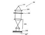
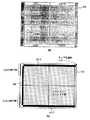
次に以上のような全体構成を有する液晶装置の製造方法を図4から図7を参照して説明する。ここに、図4は、本実施の形態における製造方法の特徴的な工程である投影露光工程におけるステッパーに用いるガラスマスク上のセルの配置図であり、図5は、ステッパーにより図4のガラスマスクを用いた投影露光工程を示す概念図、図6は、図5のステッパーにより図4に対応してマザー基板上に焼き付けられるセルの配置図である。また、図7(a)はマザー基板から切り離した1個の液晶装置に対応する1個のTFTアレイ基板におけるセル配置図であり、図7(b)は、図7(a)のTFTアレイ基板から構成される液晶装置の平面図である。
【0049】
以下に、本実施の形態における製造方法を順を追って説明する。
【0050】
先ず、薄膜形成工程では、ガラス基板、シリコン基板、石英基板等の公知の基板上に直接或いは必要に応じて下地膜としての絶縁膜を介して、画素部や駆動回路のTFT、容量、抵抗器等の回路素子や配線などに対応する所定パターンにパターニングすべき半導体膜、ポリシリコン膜、金属膜等の薄膜がCVD(Chemical Vapor Deposition)等の公知技術により形成される。
【0051】
その後、フォトレジスト塗布工程では、以上のように形成された薄膜上に、ポジ型又はネガ型の公知のフォトレジストが塗布される。
【0052】
ここで、本実施の形態では特に、縮小投影露光工程において、ステッパーによる一回の露光(ステッパーショット)で露光される露光領域は、X方向及びY方向に複数の所定ブロック領域に予め分割されている。このようなステッパーによる縮小投影露光のために、例えば、図4に示したセル配置を持つガラスマスク(レチクル)330が用意される。ガラスマスク330は、ソーダガラス、低膨張ガラス、石英ガラス等の公知の材料からなり、その遮光部331には、クロムなどの金属膜が形成されている。また、図4には、露光性能保証範囲が、円で示されている。
【0053】
図4において、ガラスマスク330は、マザー基板上で画素部を形成するためのブロック領域CGSOを、該画素部を構成する回路素子、配線等に対応する所定パターンで露光するためのマスク領域CGSO’が設けられている。マスク領域CGSO’の上下には、マザー基板上で信号線駆動回路を形成するためのブロック領域CXTL、CXTR、CXBL及びCXBRを、該信号線駆動回路を構成する回路素子、配線等に対応する所定パターンで露光するためのマスク領域CXTL’、CXTR’、CXBL’及びCXBR’が設けられている。マスク領域CGSO’の左右には、マザー基板上で走査線駆動回路を形成するためのブロック領域CYTL、CYTR、CYBL及びCYBRを、該走査線駆動回路を構成する回路素子、配線等に対応する所定パターンで露光するためのマスク領域CYTL’、CYTR’、CYBL’及びCYBR’が設けられている。更に、マザー基板に複数形成されたTFTアレイ基板の各々を該マザー基板から切り離す際に各TFTアレイ基板から切り離されるマザー基板の周辺部分において、各種のテストパターン、静電破壊防止用パターンなどの付加的配線等を形成するためのブロック領域BT、BL、BB、BR、BT、BTR、BTL、BBR、BBL、BTSL、BTSR、BBSL及びBBSRを、該付加的配線等に対応する所定パターンで露光するためのマスク領域BT’、BL’、BB’、BR’、BT’、BTR’、BTL’、BBR’、BBL’、BTSL’、BTSR’、BBSL’及びBBSR’が設けられている。更に、露光時の位置合わせ用マークRPAMKが、ガラスマスク330の4角に近い露光性能保証範囲に4個設けられている。
【0054】
以上のように構成されたガラスマスク330は、図5に示すようにステッパー300にセットされる。そして、ガラスマスク330には、露光用光源310から発せられコリメータレンズ320により平行光とされた光が入射される。ステッパー300では、ガラスマスク330の遮光パターンに応じた縮小像を、縮小投影レンズ系340を介して、マザー基板100’上に塗布されたフォトレジスト350の上に投影結像する。そして、特に上述した各種のブロック領域毎に露光(ステッパーショット)を行い、マザー基板100’をステップ移動しながら、この露光を繰り返して行うことによりマザー基板100’上のフォトレジスト全面を露光する。
【0055】
本実施の形態では、図4に示したガラスマスク330及び図5に示したステッパー300を用いて縮小投影露光を行い、例えば図6に示すように、一枚のマザー基板100’には6つのTFTアレイ基板100が形成される。
【0056】
更に、図7(a)に示すように、各TFTアレイ基板100における画面表示領域は、4つのブロック領域CGSOに分割されており、4回のステッパーショットにより露光される。また、信号線駆動回路が形成される領域は、4つのブロック領域CXTL、CXTR、CXBL及びCXBRに分割されており、4回のステッパーショットにより露光される。更にまた、走査線駆動回路が形成される領域は、2つのブロック領域CYTL及びCYBLに分割されており、2回のステッパーショットにより露光される。そして、各ブロック領域の境界には、後述のように回路素子が形成されることなく配線のみが形成され、各ブロック領域の境界(即ち、露光境界)における各配線の寸断を防止するために、各ブロック領域の境界は2重露光される。
【0057】
尚、図7(b)に示した例では、走査線駆動回路102は、画面表示領域の左側にのみ形成されているが、特に信号線駆動回路101b、101b’は、画面表示領域の上下に分割して形成されている。より具体的には偶数番目の信号線を駆動するドライバ回路セルが全て下側に配置されており、奇数番目の信号線を駆動するドライバ回路セルが全て上側に配置されている(この構成については、後に詳述する)。但し、信号線駆動回路を上側又は下側のみに形成してもよいし、走査線駆動回路を左右に分割して形成してもよい。
【0058】
本実施の形態では特に、以上のように構成されたガラスマスク330を用いてブロック領域毎に縮小投影露光を行う際に、信号線駆動回路については、図4に示したガラスマスク330を介して、信号線毎に設けられた複数のドライバ回路セルがX方向に画素ピッチよりも小さい所定ピッチを持つように当該露光が行われる。また、走査線駆動回路については、図4に示したガラスマスク330を介して、走査線毎に設けられた複数のドライバ回路セルがY方向に画素ピッチよりも小さい所定ピッチを持つように当該露光が行われる。このようにして一のブロック領域における露光が完了する度に、図5において、ステッパー300によるステップ移動が行われて、露光用光源310に対してマザー基板100’が相対的に移動され、他のブロック領域が繰り返し露光される。この繰り返しにより、図4に示した1枚のガラスマスク330を用いて、図6に示したようなブロック毎の露光を順次行うことが可能となる。
【0059】
そして、素子形成工程においては、ドライエッチング、ウエットエッチング、フォトレジスト除去等により、露光されたフォトレジスト350を用いて前述の半導体膜、ポリシリコン膜、金属膜等の薄膜が、形成すべき素子に対応するパターンで、パターニングされる。これにより、複数の画素部及びドライバ回路セルを夫々構成するTFT、容量、抵抗器等の回路素子が少なくとも部分的に形成される。以上により、例えば、単一層構造を有する抵抗等の回路素子や配線であれば完成し、また積層構造を持つTFT、容量等の回路素子であれば、必要に応じて層間絶縁膜等やコンタクトホールを形成しつつ、上記薄膜形成工程から素子形成工程までを素子の積層構造に応じて複数回行うことにより、素子が完成する。
【0060】
以上の結果、本実施の形態によれば、信号線駆動回路を構成する複数のドライバ回路セルは、各ブロック領域CXTL、CXTR等においてX方向の画素ピッチよりも小さいピッチで形成される。
【0061】
すると、図6及び図7(a)において、各ブロック領域CXTL、CXTR、CXBL及びCXBR各々の内部における境界近傍には、ドライバ回路セルを形成しない領域が発生することになる。好ましくは、ドライバ回路セルを各ブロック領域においてX方向についての中央に寄せることにより、各ブロック領域CXTL、CXTR等の各々における左右両側の境界近傍で、ドライバ回路セルを形成しない領域が発生するようにする。
【0062】
従って、ドライバ回路セルを構成するTFT、容量、抵抗器等の回路素子を、ブロック領域CXTL、CXTR等の境界、即ち露光境界を跨るように形成する必要が無くなり、これらの回路素子に継目部分を含ませないで済む。ここで一般の場合、露光境界の継目部分には、配線や素子の寸断を防止するための2重露光に起因して、パターン寸法にバラツキが生じるが、本実施の形態の場合、このような継目部分におけるパターン寸法のバラツキがこれらの回路素子の特性のバラツキとなって現われる事態を未然に防止できる。
【0063】
以上の結果、性能が安定しており信頼性の高いドライバ回路セルから信号線駆動回路を構成できる。
【0064】
他方、走査線駆動回路を構成する複数のドライバ回路セルは、各ブロック領域CYTL、CYBLにおいてY方向の画素ピッチよりも小さいピッチで形成される。従って、信号線駆動回路の場合と同様に、各ブロック領域CYTL、CYTRの境界近傍には、ドライバ回路セルを形成しない領域が発生するため、ドライバ回路セルを構成するTFT、容量、抵抗器等の回路素子に継目部分を含ませないで済む。この結果、性能が安定しており信頼性の高いドライバ回路セルから走査線駆動回路を構成できる。
【0065】
これらに加えて、本実施の形態では、ステッパーを用いてブロック領域毎に露光を行うので、例えば、対角10インチやそれ以上の大型の電気光学装置であっても、ステッパーを用いて当該縮小投影露光を行うことが可能となる。即ち、ブロック領域の数を増加させれば、マザー基板100’上で任意の大きさのTFTアレイ基板100を露光することも可能となるし、また、マザー基板100’の大きさを大きくしてもよい。従って、ステッパーの有する利点である、回路素子や配線などの微細化を、大型の液晶装置においても生かすことができ、回路素子の高速化、配線の低容量化、低消費電力化、高解像度化、装置全体の小型薄型化などを図ることができる。
【0066】
以上の結果、本実施の形態の製造方法によれば、ステッパー技術を利用して、複数のドライバ回路セルから構成される信号線駆動回路及び走査線駆動回路を内蔵すると共に高性能且つ大型の電気光学装置を比較的効率良く且つ低コストで製造できる。
【0067】
尚、本実施の形態では特に、図4に示したように、マザー基板100’上に複数形成されるTFTアレイ基板100(図6参照)の各々を識別するための識別パターンの一例として、例えばアルファベットA、B、C、…や数字1、2、3、…からなるチップ名挿入用パターンがガラスマスク330に形成されており、このガラスマスク330を用いて縮小投影露光を行うことにより、図6及び図7に示したように、各基板にチップ名識別パターンを焼き付けることができる。特にA1、A2、…といた具合に、文字や数字を組み合わせてチップ名とすれば、同一マザー基板100’上に数十枚のTFTアレイ基板100を焼き付ける場合にも、各TFTアレイ基板100に固有のチップ名を付けることが可能となる。従って、大型のマザー基板を用いてステッパーにより当該電気光学装置を大量生産をする際に大変便利である。
【0068】
(液晶装置の細部構成)
次に以上のように製造された液晶装置の細部構成について図8及び図9を参照して説明する。ここに、図8は、信号線駆動回路のドライバ回路セルを画面表示領域の上側にのみ形成した場合の信号線駆動回路及び画素部の部分的な拡大平面図であり、図9は、信号線駆動回路のドライバ回路セルを画面表示領域の上下両側に分割形成した場合の信号線駆動回路及び画素部の部分的な拡大平面図である。
【0069】
先ず、図8を参照して、以上説明した製造方法により製造される液晶装置の細部構成の一例について説明する。
【0070】
図8において、信号線駆動回路101aの複数のドライバ回路セル200aは、信号線41毎に設けられている。各々の信号線41は、RGBのカラーフィルタが夫々設けられた各画素のTFTのソース又はドレインに接続されている。各ドライバ回路セル200aは、X方向に沿って延びる画像信号線250aを介して入力されるデジタル画像信号を、該デジタル画像信号の示す階調に応じた駆動電圧を持つアナログ画像信号に変換して各信号線41に供給するように構成されている。
【0071】
ここで本実施の形態では特に、ドライバ回路セル200aの形成ピッチは、X方向についての画素ピッチよりも、例えば数パーセント程度小さく設定されているので、各ブロック領域内において中央側の大部分が素子形成領域210とされると共に、各ブロック領域の境界近傍が配線専用領域220とされる。そして、駆動回路部における配線専用領域220には、ドライバ回路セル200aは設けられることはなく、画像信号線250aのみが設けられている。
【0072】
即ち、本実施の形態では、投影露光により、画像信号配線250aは、各ブロック領域の境界を跨ぐ継目部分を含むように形成されている。画像信号線250aは金属膜や導電性ポリシリコン膜等からなり、基本的に電気信号を伝達するという単純機能を果たせばよいので、断線やリークさえなければ、この継目部分における薄膜部分のバラツキによる抵抗や容量変化が問題となることは実用上殆ど又は全く無い。そして、画像信号線250aが露光境界(ブロック領域の境界)を跨ってX方向に延びることにより、複数のブロック領域に跨る複数のドライバ回路セル200a間を電気的接続できる。同様に、画素部において、金属膜や導電性ポリシリコン膜等から構成される信号線41や走査線42についても、露光境界では、継目部分を介して接続されており、画素部のTFT30が継目部分を含むことはない。この結果、当該電気光学装置を一つの装置として機能させられる。
【0073】
そして、このように配線専用領域220において、TFT、容量、抵抗器等の回路素子に継目部分を含ませないで済むので、継目部分における薄膜部分のバラツキがこれらの素子の特性のバラツキとなって現われる事態を確実に未然に防止できるのである。
【0074】
また本実施の形態では特に、図8に示すように、配線専用領域220において、上述の投影露光により画像信号線250aの継目部分が幅広に形成されている。従って、ブロック領域に対する露光が境界に沿って多少ずれても、この幅広の継目部分の広さに応じて継目部分における電気的接続を良好にとることができる。他方、前述のように露光境界に直交する方向については、従来通りに、両方の露光領域を重ねる(即ち、2重露光する)ことにより、画像信号線250aの継目部分が形成されている。従って、ステッパーにおける露光位置精度が多少低くても、画像信号線250aの電気的接続が良好にとれる限りは問題は生じないので、製造上大変有利である。また、ブロック領域の境界における信号線41や走査線42の継目部分についても同様に幅広に且つ2重露光により形成されている。
【0075】
また図8に示すように、本実施の形態では特に、前述の等倍投影露光により、画面表示領域内外の境界に、信号線41のピッチを画素ピッチからドライバ回路セル200aの形成ピッチに変換する配線ピッチ変換部230が形成されている。このため、画素ピッチとドライバ回路セル200aの形成ピッチとが相異なっていても、両者間の電気的接続を配線ピッチ変換部により良好にとることができる。
【0076】
尚、本実施の形態では好ましくは、信号線駆動回路101aを構成するスイッチング素子、走査線駆動回路を構成するスイッチング素子及び画素部を構成するスイッチング素子を、同一構成を持つ薄膜トランジスタから構成する。このようすれば、同一のTFTアレイ基板100上に同一製造工程で駆動回路及び画素部を形成できるので、製造上有利である。
【0077】
次に、図9を参照して、以上説明した製造方法により製造される液晶装置の細部構成の他の例について説明する。
【0078】
図9において、信号線駆動回路101b及び101b’は、画面表示領域の上下に分割して設けられており、上側の信号線駆動回路101bを構成するドライバ回路セル200bは、奇数番目の信号線41に夫々接続されており、下側の信号線駆動回路101b’を構成するドライバ回路セル200b’は、偶数番目の信号線41に夫々接続されている。各々の信号線41は、RGBのカラーフィルタが設けられた各画素のTFTのソース又はドレインに接続されている。各ドライバ回路セル200b、200b’は、図8に示した例の場合と同様に、画像信号線250aを介して入力されるデジタル画像信号を、該デジタル画像信号の示す階調に応じた駆動電圧を持つアナログ画像信号に変換して各信号線41に供給するように構成されている。
【0079】
ここで、本実施の形態では特に、ドライバ回路セル200b、200b’の形成ピッチは、画素ピッチよりも、例えば数パーセント程度小さい。より具体的には、片側のドライバ回路セル200b又は200b’の形成ピッチは夫々、画素ピッチの2倍よりも数パーセント程度小さい(即ち、画素ピッチDpとドライバ回路セル200b又は200b’の形成ピッチDdとは、Dd<2・Dpという関係が成立している)ので、各ブロック領域内において中央側の大部分が素子形成領域210とされると共に、各ブロック領域の境界近傍が配線専用領域220とされる。そして、駆動回路部における配線専用領域220には、ドライバ回路セル200b、200b’は設けられることはなく、X方向に延びる画像信号線250bのみが設けられている。
【0080】
即ち、本実施の形態では図8に示した例の場合と同様に、ドライバ回路セル200b、200b’や画素部を構成する回路素子に継目部分を含ませないで済むので、継目部分における薄膜部分のバラツキがこれらの回路素子の特性のバラツキとなって現われる事態を確実に未然に防止できる。
【0081】
これに加えて図9に示した例では、上下に分割された各信号線駆動回路101b、101b’が相互に入り組んで配置されることにより、全体としてコンパクトな構成となっている。即ち、信号線駆動回路101b、101b’を分割したことにより、各信号線駆動回路を構成する素子の数が1/2となり、一つにまとめてこれらの回路を夫々形成する場合と比較して、各回路による占有面積が夫々減り、各回路について余裕を持った素子の配置や配線が可能となる。特に中央に画像表示領域があると共にその上下に周辺領域がある液晶パネル等の電気光学パネルに対しては、当該上下の周辺領域にバランス良く余裕を持った素子の配置や配線が可能となる。また、このように分割することは、回路の均等配置を可能ならしめるものであり、TFTアレイ基板上におけるデッドスペースの有効利用を図れる。例えば、液晶パネルの場合、前述のシール材直下にあるデッドスペースを活用できる(図2及び図3参照)。即ち、シール材は、基板に余分な応力を与えないように基板の周囲に均等の幅で接するように設けられているので、回路を分割して各回路の素子数を低減して、各回路をシール材直下の領域の形状に合わせて均等に配置すればよい。そして、この種の液晶パネルのように画素ピッチにより走査線に沿った一方向についての回路素子のピッチが特に制約を受ける場合には、本実施の形態は有効である。更に、信号線駆動回路が含むシフトレジスタ回路(図1参照)の段数が、図8に示した例の場合と比較して半分になるため、動作周波数も1/2になり、回路設計上有利である。
【0082】
尚、本実施の形態において、ドライバ回路セル200b、200b’を構成するDAコンバータとしては、前述のようにSC―DAC(Switched Capacitor - Digital to Analog Converter)回路が好ましい。このように構成すれば、SC−DAC回路を構成する、例えば容量やTFT等の素子は、露光境界における継目部分を含まないため、継目部分のバラツキに影響されない。特に、基板上に作り込まれる容量におけるバラツキを低減することはSC−DAC回路の出力電圧の精度を向上するのに役立つので、上述した本実施の形態の効果が顕著に発揮される。この結果、デジタル画像信号を高精度でアナログ画像信号に変換でき、このアナログ画像信号を用いて画素部を駆動することにより、高品位の階調表示等を実現できる。尚、SC−DAC回路以外のDAコンバータを用いて信号線駆動回路を構成しても、上述した本実施の形態の効果は発揮される。また、本実施の形態では、縮小投影について説明されているが、縮小投影に限らず、等倍投影についても同様な構成及び効果が得られることは言うまでもない。
【0083】
以上のように本実施の形態の液晶装置によれば、上述した製造方法により製造されるため、駆動回路を内蔵した液晶装置において、大型化を図りつつ性能を高めることが可能となる。
【0084】
【発明の効果】
以上詳細に説明したように本発明によれば、ステッパー技術を利用して、複数の第1方向駆動回路セルから構成される駆動回路を内蔵すると共に高性能且つ大型の電気光学装置を比較的効率良く且つ低コストで製造できる。
【図面の簡単な説明】
【図1】本発明による液晶装置の実施の形態における全体回路構成を示すブロック図である。
【図2】液晶装置の実施の形態における全体構成を示す平面図である。
【図3】図2のH−H’断面図である。
【図4】本発明による製造方法の実施の形態におけるステッパーに用いられるガラスマスクのセルの配置図である。
【図5】製造方法の実施の形態における、ステッパーを使用した投影露光工程の概念図である。
【図6】図5のステッパーにより図4に対応してマザー基板上に焼き付けられるセルの配置図である。
【図7】マザー基板から切り離した1個の液晶装置に対応する1個のTFTアレイ基板におけるセルの配置図(図7(a))及び、図7(a)のTFTアレイ基板から構成される液晶装置の平面図(図7(b))である。
【図8】本発明による液晶装置の細部構成の一例を示す部分拡大平面図である。
【図9】本発明による液晶装置の細部構成の他の例を示す部分拡大平面図である。
【符号の説明】
10…シフトレジスタ回路
20…対向基板
30…TFT
40…画素電極
41…信号線
42…走査線
100…TFTアレイ基板
100’…マザー基板
101…信号線駆動回路
102…走査線駆動回路
200…ドライバ回路セル
210…素子形成領域
220…配線専用領域
230…配線ピッチ変換領域
300…ステッパー
310…露光用光源
330…ガラスマスク[0001]
BACKGROUND OF THE INVENTION
The present invention belongs to a manufacturing method for manufacturing an electro-optical device such as a liquid crystal panel and the technical field of the electro-optical device, and particularly, a large-sized and high-detailed image using a projection exposure apparatus (hereinafter referred to as “stepper” as appropriate). Technical field of a method for manufacturing an electro-optical device suitable for manufacturing an electro-optical device such as a liquid crystal panel of an active matrix driving system with a built-in driver (the pixel portion and the driver circuit are formed on the same substrate) and The electro-optical device thus manufactured belongs to the technical field.
[0002]
[Prior art]
In the technical field of a method of manufacturing a semiconductor device such as a large-scale integrated circuit (LSI), a technique of manufacturing a large number of semiconductor devices having the same configuration in a matrix on a single large wafer is common. During this manufacturing process, an exposure process is performed in which a photoresist is exposed through a mask in order to pattern various thin films such as semiconductor films and metal films. However, in mass production, reduction suitable for miniaturization and mass production. Projection exposure is usually performed. That is, a reduced projection exposure apparatus called a stepper projects a reduced image of an enlarged size mask (reticle) onto a wafer, performs exposure for one chip to several chips at the same time, and moves the wafer step by step. The entire wafer is exposed by repeating the exposure.
[0003]
Conventionally, when manufacturing an electro-optical device such as a TFT active matrix driving type liquid crystal panel with a built-in driver, which includes a large number of thin film transistors (hereinafter referred to as “TFT” as appropriate), the liquid crystal panel is not suitable. If it is small and has a size of about 1 inch square, the substrate portion that constitutes one or more liquid crystal panels or the like on the mother substrate by one exposure by the stepper, as in the case of manufacturing the semiconductor device described above. Can be exposed simultaneously. Accordingly, miniaturization can be achieved as in the case of a semiconductor device, and mass production of a plurality of liquid crystal panels and the like can be efficiently performed from one large mother substrate. In this case, in particular, due to the difference in the wiring length to each driving circuit cell (that is, one unit for driving the signal line in the driving circuit) constituting the driver unit and the wiring length to each pixel unit in the screen display area, The pixel pitch in the screen display area and the drive circuit cell in the driver section are arranged so that the driver section can be compactly fitted in a narrow area around the screen display area so that a difference in drive voltage output from each drive circuit cell does not occur. The pitch is the same. A drive circuit cell for driving the signal line is regularly connected to one end of each of the plurality of signal lines arranged in the screen display area.
[0004]
Such projection exposure by a stepper is not suitable for the purpose of simultaneously exposing a too large area for projection. That is, as the area to be exposed at the same time is increased, the exposure throughput decreases, the imaging state and alignment at each point in the exposure area become difficult, and the exposure accuracy also decreases. Therefore, in practice, a stepper is not used when manufacturing a liquid crystal panel or the like having a pixel portion and a driver circuit on a large substrate having a diagonal size of about 10 inches, for example.
[0005]
On the other hand, as a technique using a stepper, when a large circuit is manufactured, only a part of a region that becomes a large circuit is exposed by one exposure, and a single large circuit is formed by a plurality of exposures. There is a technique for exposing an area. In this technique, in particular, it is necessary to take care so that wirings, elements, and the like are not cut off at a boundary between regions exposed separately (hereinafter referred to as “exposure boundary”). For this reason, at the exposure boundary, both exposure areas are overlapped (that is, double exposure is performed) so as to form a joint portion such as a wiring or an element. In the case of such a large circuit, not only a reduced projection but also an equal magnification projection is often used.
[0006]
Therefore, even when a liquid crystal panel is manufactured using this technology, if the liquid crystal panel is large and is not of a built-in driver type, the technology using the above-mentioned stepper is subject to loose design rules for wiring and the like. Thus, the liquid crystal panel can be manufactured while including many seam portions. That is, since it is not necessary to form a peripheral circuit (driver unit) including complicated elements on the substrate of the liquid crystal panel, an external driver circuit can be connected to the TAB later even if there are some joints or loose design rules. If connected by (tape automated bonding) or the like, a large liquid crystal panel with few practical problems can be manufactured using a stepper.
[0007]
[Problems to be solved by the invention]
However, in the case of an electro-optical device such as a liquid crystal panel with a built-in driver, it is necessary to form a driver unit including a number of complicated circuit elements around the screen display area on the substrate. If the size is increased, manufacturing using the above-mentioned stepper becomes difficult. However, since the entire region corresponding to the substrate portion constituting one large liquid crystal panel cannot be exposed by a single exposure using a stepper, a plurality of joint portions as described above must be present. This is because it is practically difficult to construct a large number of complicated drive circuits so as to include a simple seam portion. In particular, when creating a relatively complex drive circuit including circuit elements such as TFTs, resistors, capacitors, etc. that handle analog signals, the variation in the thin film portion at the joint portion becomes the variation in the characteristics of these circuit elements. If such a large liquid crystal panel with a built-in driver is simply manufactured using a stepper, there is a problem that the performance is extremely unstable or the reliability is insufficient.
[0008]
On the other hand, when a large liquid crystal panel with a built-in driver is manufactured by one exposure using an aligner or the like without using a stepper, for example, about several μm is a practical meaning of miniaturization. Therefore, it is impossible to reduce the size to about 1 μm or less that can be realized at a relatively low cost by using a stepper. Therefore, there is a problem that due to miniaturization of elements such as TFTs and wiring, it is impossible to increase the speed of the elements, reduce the capacity of the wiring, reduce the power consumption, increase the resolution, and reduce the overall size and thickness of the device. is there.
[0009]
The present invention has been made in view of the above-described problems, and a method for manufacturing an electro-optical device that includes a drive circuit and can manufacture a high-performance and large-sized electro-optical device using a stepper, and the method. It is an object to provide an electro-optical device.
[0010]
[Means for Solving the Problems]
In order to solve the above-described problem, a method for manufacturing an electro-optical device according to an embodiment of the present invention includes a screen including a plurality of pixel portions arranged in a matrix on a substrate in a first direction and a second direction intersecting the first direction. A plurality of first-direction drive circuit cells for driving the plurality of pixel portions, which are provided around the display region in correspondence with the display region and the arrangement of the plurality of pixel portions in the second direction, respectively. An electro-optical device manufacturing method for manufacturing an electro-optical device comprising: a thin film forming step for forming a thin film to be patterned on the substrate; and a photoresist forming step for forming a photoresist on the thin film. The plurality of pixel portions have a predetermined first pitch in the first direction for each predetermined block region obtained by dividing the region where the photoresist is formed into at least a plurality of the first direction. A projection exposure step of performing projection exposure with a light source for exposure through a mask of a predetermined pattern so that the first direction driving circuit cell has a predetermined second pitch smaller than the predetermined first pitch in the first direction; A step of sequentially moving the substrate relative to the exposure light source to expose another block region after exposing one block region in the process, and the thin film using the exposed photoresist Forming a plurality of elements respectively constituting the plurality of pixel portions and the plurality of first direction driving circuit cells by patterning, and in the projection exposure step and the movement step, A wiring pin including a plurality of wirings that connect the plurality of pixel portions and the plurality of first direction driving circuit cells to each other at the boundary between the inside and outside of the screen display area. Exposure and moves so as to form a conversion unit, in the device forming step, characterized in that the wiring pitch conversion unit further formed.
[0011]
According to the present invention, first, a thin film to be patterned is formed on the substrate in the thin film forming step, and a photoresist is formed on the thin film in the photoresist forming step. Here, in the projection exposure step, the exposure area is divided in advance into a predetermined block area divided into a plurality of parts in at least the first direction. Then, for each block region, a plurality of pixel portions have a predetermined first pitch in the first direction, and a plurality of first direction driving circuit cells have a predetermined second pitch smaller than the predetermined first pitch in the first direction. Thus, projection exposure is performed by an exposure light source through a mask having a predetermined pattern. Here, each time one block area is exposed by the projection exposure process, the moving process sequentially moves the substrate relative to the exposure light source, and the other block areas are repeatedly exposed. In the element formation step, the thin film is patterned using an exposed photoresist by etching or the like, and the plurality of elements that respectively constitute the plurality of pixel portions and the plurality of first direction driving circuit cells are at least partially It is formed.
[0012]
Accordingly, since the plurality of first direction driving circuit cells are formed at the second pitch smaller than the first pitch which is the pixel pitch in each block region, the TFTs, capacitors, resistors, and the like constituting the first direction driving circuit cell These circuit elements can be arranged without being formed so as to straddle the boundary of the block region, that is, the exposure boundary. As a result, it is possible to prevent a situation in which variations in the thin film portion at the joint portion appear as variations in characteristics of these circuit elements, and it is possible to form a first direction drive circuit cell with stable performance and high reliability. Further, according to the configuration of the present invention, the wiring pitch conversion unit including the plurality of wirings that connect the plurality of pixel units and the plurality of first direction driving circuit cells to each other is formed at the boundary between the inside and the outside of the screen display region. Is done. Therefore, even if the pixel pitch and the pitch of the first direction driving circuit cells are different, the wiring pitch converter can make electrical connection between them.
[0013]
In addition, since exposure is performed for each block area, for example, even a large electro-optical device having a diagonal of 10 inches or more can perform the projection exposure using a stepper. Therefore, by miniaturizing elements such as TFTs and wiring, it is possible to increase the speed of the elements, reduce the capacity of the wiring, reduce power consumption, increase the resolution, and reduce the overall size and thickness of the device.
[0014]
As a result, according to the present invention, a stepper technique is used to incorporate a drive circuit composed of a plurality of first-direction drive circuit cells and to make a high-performance and large electro-optical device relatively efficient and low. Can be manufactured at low cost.
[0021]
The electro-optical device manufacturing method of the present invention is further provided around the screen display area corresponding to the arrangement of the plurality of pixel portions in the first direction, and the plurality of pixel portions are provided on the substrate. A plurality of second direction driving circuit cells for driving the pixel portion, and a predetermined block formed by dividing the region in which the photoresist is formed into the second direction in the projection exposure step; For each region, the plurality of pixel portions have a predetermined third pitch in the second direction, and the plurality of second direction drive circuit cells have a predetermined fourth smaller in the second direction than the predetermined third pitch. The exposure is performed so as to have a pitch.
[0022]
According to this configuration of the present invention, in the projection exposure step, the exposure area is divided in advance into predetermined block areas that are divided in the second direction in addition to the first direction. For each block region, the plurality of pixel portions have a predetermined third pitch in the second direction, and the plurality of second direction driving circuit cells have a predetermined fourth pitch smaller than the predetermined third pitch in the second direction. Thus, projection exposure is performed by an exposure light source through a mask having a predetermined pattern.
[0023]
Accordingly, since the plurality of second direction driving circuit cells are formed at the fourth pitch smaller than the third pitch, which is the pixel pitch in each block region, the second direction driving circuit cells are arranged near the boundary of each block region. Regions that will not be formed will occur. For this reason, it is not necessary to include a joint portion in circuit elements such as TFTs, capacitors, resistors, etc. constituting the second direction driving circuit cell. As a result, it is possible to prevent a situation in which variations in the thin film portion at the joint portion appear as variations in the characteristics of these circuit elements, and it is possible to form a second direction drive circuit cell with stable performance and high reliability.
[0026]
The method of manufacturing an electro-optical device according to the present invention is characterized in that the projection exposure step further performs reduction projection or equal magnification projection.
According to this configuration of the present invention, it is possible to reliably perform reduction or equal magnification projection corresponding to a predetermined mask.
[0029]
The method of manufacturing an electro-optical device according to the present invention is further characterized in that, in the element formation step, a thin film transistor is formed as the element.
[0030]
According to this configuration of the present invention, a thin film transistor is formed as an element of the first direction driving circuit cell or the pixel portion. Accordingly, the driving circuit and the pixel portion can be formed using thin film transistors having the same film structure on the substrate, which is advantageous in manufacturing.
[0031]
The electro-optical device of the present invention is manufactured by the above-described method for manufacturing an electro-optical device.
[0032]
According to the configuration of the present invention, since it is manufactured by the above-described manufacturing method of the present invention, it is possible to improve the performance while increasing the size of the electro-optical device incorporating the drive circuit.
[0033]
In the electro-optical device according to the aspect of the invention, the plurality of pixel portions each include a pixel switching thin film transistor, and a signal line driving driver circuit is configured from the plurality of first direction driving circuit cells on the substrate. It is characterized by that.
[0034]
According to such a configuration of the present invention, in an active matrix driving type liquid crystal device in which a driving circuit for driving a signal line is formed on the same substrate as a pixel portion, it is possible to improve performance while increasing the size.
[0037]
In the electro-optical device according to the aspect of the invention, the first direction driving circuit cell may be provided around the screen display area along two opposite sides of the screen display area, and one of the two sides. The first direction driving circuit cell corresponding to the odd-numbered array of the plurality of pixel portions in the second direction is provided around the other side of the two sides, The first direction drive circuit cell corresponding to an even-numbered array of the plurality of pixel portions in the second direction is provided.
[0038]
According to such a configuration of the present invention, the first direction driving circuit cell is provided, for example, in half each in the upper peripheral region and the lower peripheral region of the screen display region. Compared to the above, the formation pitch of the first direction drive circuit cells can be halved, and the first direction drive circuit cells can be formed with a margin, and the peripheral area of the screen display area is effectively balanced. It can also be used.
[0039]
Such an operation and other advantages of the present invention will become apparent from the embodiments described below.
[0040]
DETAILED DESCRIPTION OF THE INVENTION
Hereinafter, embodiments of the present invention will be described with reference to the drawings.
[0041]
(Overall configuration of liquid crystal device)
First, as an example of an electro-optical device manufactured by the manufacturing method of the present invention, the overall configuration of a TFT active matrix driving type and driver built-in type liquid crystal device will be described with reference to FIGS. 1 is a block diagram showing a circuit configuration of the liquid crystal device, FIG. 2 is a plan view of the liquid crystal device, and FIG. 3 is a cross-sectional view taken along line HH ′ of FIG.
[0042]
In FIG. 1, a screen display region located at the center on the
[0043]
The signal
[0044]
On the other hand, the scanning
[0045]
As will be described later, the pitch in the X direction of the
[0046]
2 and 3, a sealing
[0047]
A
[0048]
(Manufacturing method of liquid crystal device)
Next, a method for manufacturing a liquid crystal device having the overall configuration as described above will be described with reference to FIGS. FIG. 4 is a layout diagram of cells on the glass mask used for the stepper in the projection exposure process which is a characteristic process of the manufacturing method according to the present embodiment. FIG. 5 is a diagram illustrating the glass mask of FIG. FIG. 6 is a conceptual diagram showing a projection exposure process using the, and FIG. 6 is a layout diagram of cells to be printed on the mother substrate by the stepper of FIG. 5 corresponding to FIG. FIG. 7A is a cell layout diagram of one TFT array substrate corresponding to one liquid crystal device separated from the mother substrate, and FIG. 7B is a TFT array substrate of FIG. 7A. It is a top view of the liquid crystal device comprised from these.
[0049]
Below, the manufacturing method in this Embodiment is demonstrated later on.
[0050]
First, in the thin film formation process, TFTs, capacitors, resistors of the pixel portion and the drive circuit are directly or on an insulating film as a base film on a known substrate such as a glass substrate, a silicon substrate, or a quartz substrate, if necessary. A thin film such as a semiconductor film, a polysilicon film, or a metal film to be patterned into a predetermined pattern corresponding to a circuit element such as a circuit element or wiring is formed by a known technique such as CVD (Chemical Vapor Deposition).
[0051]
Thereafter, in the photoresist application step, a known positive or negative photoresist is applied onto the thin film formed as described above.
[0052]
Here, in the present embodiment, in particular, in the reduced projection exposure process, the exposure area exposed by one exposure (stepper shot) by the stepper is divided in advance into a plurality of predetermined block areas in the X direction and the Y direction. Yes. For such reduced projection exposure by the stepper, for example, a glass mask (reticle) 330 having the cell arrangement shown in FIG. 4 is prepared. The
[0053]
In FIG. 4, a
[0054]
The
[0055]
In the present embodiment, reduction projection exposure is performed using the
[0056]
Further, as shown in FIG. 7A, the screen display area in each
[0057]
In the example shown in FIG. 7B, the scanning
[0058]
Particularly in the present embodiment, when performing reduction projection exposure for each block region using the
[0059]
In the element formation step, the thin film such as the semiconductor film, the polysilicon film, or the metal film is formed on the element to be formed by using the exposed
[0060]
As a result, according to the present embodiment, the plurality of driver circuit cells constituting the signal line driver circuit are formed at a pitch smaller than the pixel pitch in the X direction in each block region CXTL, CXTR, and the like.
[0061]
Then, in FIG. 6 and FIG. 7A, a region where no driver circuit cell is formed is generated in the vicinity of the boundary inside each block region CXTL, CXTR, CXBL, and CXBR. Preferably, by bringing the driver circuit cell to the center in the X direction in each block region, a region in which no driver circuit cell is formed is generated in the vicinity of the left and right boundary in each block region CXTL, CXTR, etc. To do.
[0062]
Therefore, there is no need to form circuit elements such as TFTs, capacitors, resistors, etc. constituting the driver circuit cell so as to straddle the boundaries of the block regions CXTL, CXTR, etc., that is, the exposure boundaries. Do not include. Here, in general cases, the pattern size varies at the joint portion of the exposure boundary due to the double exposure for preventing the disconnection of the wiring and the element. It is possible to prevent a situation in which variations in pattern dimensions at the joint portion appear as variations in characteristics of these circuit elements.
[0063]
As a result, the signal line driver circuit can be configured from driver circuit cells having stable performance and high reliability.
[0064]
On the other hand, the plurality of driver circuit cells constituting the scanning line driving circuit are formed at a pitch smaller than the pixel pitch in the Y direction in each of the block regions CYTL and CYBL. Accordingly, as in the case of the signal line driver circuit, a region where no driver circuit cell is formed is generated in the vicinity of the boundary between the block regions CYTL and CYTR. Therefore, TFTs, capacitors, resistors, and the like constituting the driver circuit cell are generated. It is not necessary to include a seam portion in the circuit element. As a result, a scanning line driving circuit can be configured from driver circuit cells having stable performance and high reliability.
[0065]
In addition to the above, in this embodiment, since exposure is performed for each block region using a stepper, for example, even in a large electro-optical device having a diagonal size of 10 inches or more, the reduction is performed using a stepper. Projection exposure can be performed. That is, if the number of block regions is increased, it becomes possible to expose the
[0066]
As a result of the above, according to the manufacturing method of the present embodiment, a signal line driving circuit and a scanning line driving circuit constituted by a plurality of driver circuit cells are built in using a stepper technique, and a high-performance and large-scale electric circuit is built. The optical device can be manufactured relatively efficiently and at low cost.
[0067]
In the present embodiment, as shown in FIG. 4, as an example of an identification pattern for identifying each of a plurality of TFT array substrates 100 (see FIG. 6) formed on the
[0068]
(Detailed configuration of the liquid crystal device)
Next, a detailed configuration of the liquid crystal device manufactured as described above will be described with reference to FIGS. FIG. 8 is a partially enlarged plan view of the signal line driver circuit and the pixel portion when the driver circuit cell of the signal line driver circuit is formed only above the screen display region. FIG. FIG. 4 is a partially enlarged plan view of a signal line driving circuit and a pixel portion when a driver circuit cell of a driving circuit is divided and formed on both upper and lower sides of a screen display region.
[0069]
First, an example of a detailed configuration of a liquid crystal device manufactured by the manufacturing method described above will be described with reference to FIG.
[0070]
In FIG. 8, a plurality of driver circuit cells 200a of the signal line driver circuit 101a are provided for each
[0071]
In this embodiment, in particular, the formation pitch of the driver circuit cells 200a is set to be, for example, about several percent smaller than the pixel pitch in the X direction. In addition to the
[0072]
In other words, in the present embodiment, the image signal wiring 250a is formed so as to include a seam portion straddling the boundary of each block region by projection exposure. The image signal line 250a is made of a metal film, a conductive polysilicon film, or the like, and basically has a simple function of transmitting an electric signal. Therefore, if there is no disconnection or leakage, the image signal line 250a depends on variations in the thin film portion at the joint portion. There is little or no practical use of resistance and capacitance changes. The image signal line 250a extends in the X direction across the exposure boundary (the boundary of the block area), so that the plurality of driver circuit cells 200a across the plurality of block areas can be electrically connected. Similarly, in the pixel portion, the
[0073]
In this way, in the wiring dedicated
[0074]
Further, in the present embodiment, as shown in FIG. 8, in the wiring dedicated
[0075]
As shown in FIG. 8, in the present embodiment, the pitch of the signal lines 41 is converted from the pixel pitch to the formation pitch of the driver circuit cell 200a at the boundary between the inside and outside of the screen display area by the above-described equal projection exposure. A wiring
[0076]
Note that in this embodiment mode, the switching element included in the signal line driver circuit 101a, the switching element included in the scanning line driver circuit, and the switching element included in the pixel portion are preferably formed using thin film transistors having the same structure. In this way, the driving circuit and the pixel portion can be formed on the same
[0077]
Next, another example of the detailed configuration of the liquid crystal device manufactured by the manufacturing method described above will be described with reference to FIG.
[0078]
In FIG. 9, the signal line drive circuits 101b and 101b ′ are divided into upper and lower parts of the screen display area, and the driver circuit cell 200b constituting the upper signal line drive circuit 101b has an odd-numbered
[0079]
Here, particularly in the present embodiment, the formation pitch of the driver circuit cells 200b and 200b ′ is, for example, about several percent smaller than the pixel pitch. More specifically, the formation pitch of the driver circuit cell 200b or 200b ′ on one side is about several percent smaller than twice the pixel pitch (that is, the formation pitch Dd of the pixel pitch Dp and the driver circuit cell 200b or 200b ′). (Dd <2 · Dp is established), most of the center side in each block region is the
[0080]
That is, in the present embodiment, as in the case of the example shown in FIG. 8, the driver circuit cells 200b and 200b ′ and the circuit elements constituting the pixel portion do not need to include the seam portion. Thus, it is possible to reliably prevent a situation in which the above variation appears as a variation in the characteristics of these circuit elements.
[0081]
In addition to this, in the example shown in FIG. 9, the signal line drive circuits 101b and 101b ′ divided in the vertical direction are arranged so as to interlace with each other, so that the overall configuration is compact. That is, by dividing the signal line driver circuits 101b and 101b ′, the number of elements constituting each signal line driver circuit is halved, compared with the case where these circuits are formed together as one. The area occupied by each circuit is reduced, and elements can be arranged and wired with a margin for each circuit. In particular, for an electro-optical panel such as a liquid crystal panel having an image display area at the center and peripheral areas above and below it, it is possible to arrange and wire elements with a good balance in the upper and lower peripheral areas. Further, such division makes it possible to arrange the circuits evenly, and the effective use of the dead space on the TFT array substrate can be achieved. For example, in the case of a liquid crystal panel, the dead space immediately below the sealing material can be utilized (see FIGS. 2 and 3). In other words, the sealing material is provided so as to be in contact with the periphery of the substrate with an equal width so as not to give excessive stress to the substrate. Therefore, the circuit is divided to reduce the number of elements of each circuit. May be evenly arranged according to the shape of the region directly under the sealant. This embodiment is effective when the pitch of circuit elements in one direction along the scanning line is particularly restricted by the pixel pitch as in this type of liquid crystal panel. Further, since the number of stages of the shift register circuit (see FIG. 1) included in the signal line driver circuit is halved as compared with the example shown in FIG. 8, the operating frequency is also halved, which is advantageous in circuit design. It is.
[0082]
In the present embodiment, as described above, an SC-DAC (Switched Capacitor-Digital to Analog Converter) circuit is preferable as the DA converter constituting the driver circuit cells 200b and 200b ′. With this configuration, elements such as capacitors and TFTs that constitute the SC-DAC circuit do not include the joint portion at the exposure boundary, and thus are not affected by variations in the joint portion. In particular, reducing the variation in the capacitance formed on the substrate helps improve the accuracy of the output voltage of the SC-DAC circuit, so that the effect of the above-described embodiment is remarkably exhibited. As a result, a digital image signal can be converted into an analog image signal with high accuracy, and high-quality gradation display or the like can be realized by driving the pixel portion using the analog image signal. Even when the signal line driver circuit is configured using a DA converter other than the SC-DAC circuit, the above-described effect of the present embodiment is exhibited. In the present embodiment, reduction projection is described, but it goes without saying that the same configuration and effects can be obtained not only in reduction projection but also in equal magnification projection.
[0083]
As described above, according to the liquid crystal device of the present embodiment, since it is manufactured by the above-described manufacturing method, the performance of the liquid crystal device with a built-in drive circuit can be improved while increasing the size.
[0084]
【The invention's effect】
As described above in detail, according to the present invention, a stepper technique is used to incorporate a drive circuit composed of a plurality of first direction drive circuit cells and to make a high-performance and large electro-optical device relatively efficient. Good and can be manufactured at low cost.
[Brief description of the drawings]
FIG. 1 is a block diagram showing an overall circuit configuration in an embodiment of a liquid crystal device according to the present invention.
FIG. 2 is a plan view showing the overall configuration of an embodiment of a liquid crystal device.
FIG. 3 is a cross-sectional view taken along line HH ′ of FIG.
FIG. 4 is a layout view of cells of a glass mask used for a stepper in an embodiment of a manufacturing method according to the present invention.
FIG. 5 is a conceptual diagram of a projection exposure process using a stepper in the embodiment of the manufacturing method.
6 is a layout view of cells to be baked on a mother substrate corresponding to FIG. 4 by the stepper of FIG. 5;
7 is a layout diagram of cells on one TFT array substrate corresponding to one liquid crystal device separated from the mother substrate (FIG. 7A) and the TFT array substrate of FIG. 7A. It is a top view (Drawing 7B) of a liquid crystal device.
FIG. 8 is a partially enlarged plan view showing an example of a detailed configuration of a liquid crystal device according to the present invention.
FIG. 9 is a partially enlarged plan view showing another example of the detailed configuration of the liquid crystal device according to the present invention.
[Explanation of symbols]
10: Shift register circuit
20 ... Counter substrate
30 ... TFT
40: Pixel electrode
41 ... Signal line
42 ... Scanning line
100 ... TFT array substrate
100 '... Mother board
101. Signal line driving circuit
102 Scanning line drive circuit
200: Driver circuit cell
210: Element formation region
220 ... Wiring exclusive area
230 ... wiring pitch conversion area
300 ... Stepper
310: Light source for exposure
330 ... Glass mask
Claims (7)
Translated fromJapanese前記基板上にパターニングされる薄膜を形成する薄膜形成工程と、
該薄膜上にフォトレジストを形成するフォトレジスト形成工程と、
該フォトレジストが塗布された領域を少なくとも前記第1方向に複数分割してなる所定ブロック領域毎に、前記複数の画素部が前記第1方向に第1画素ピッチを持つように且つ前記複数の第1方向駆動回路セルが前記第1方向に前記第1画素ピッチよりも小さい第1方向駆動回路セル形成ピッチを持つように所定パターンのマスクを介して露光用光源により投影露光する投影露光工程と、
該投影露光工程により一のブロック領域を露光した後に他のブロック領域を露光すべく前記基板を前記露光用光源に対して相対的に順次移動させる移動工程と、
該露光されたフォトレジストを用いて前記薄膜をパターニングすることにより前記複数の画素部及び前記複数の第1方向駆動回路セルを夫々構成する複数の素子を少なくとも部分的に形成する素子形成工程とを含み、
前記投影露光工程及び移動工程において、前記画面表示領域の周囲であって、且つ、前記各ブロック領域の境界を含む位置に、前記複数の第1方向駆動回路セルが形成されない配線専用領域が設けられ、前記画面表示領域内外の境界に、前記複数の画素部と前記複数の第1方向駆動回路セルとを相互に夫々接続する複数の配線を含む配線ピッチ変換部を形成するように露光及び移動し、前記素子形成工程において、前記配線ピッチ変換部を更に形成することを特徴とする電気光学装置の製造方法。Corresponding to a screen display area composed of a plurality of pixel portions arranged in a matrix in a first direction and a second direction intersecting the first direction on the substrate, and the arrangement of the plurality of pixel portions in the second direction An electro-optical device manufacturing method for manufacturing an electro-optical device including a plurality of first-direction drive circuit cells that are respectively provided around the screen display region and drives the plurality of pixel units. And
Forming a thin film to be patterned on the substrate;
A photoresist forming step of forming a photoresist on the thin film;
The plurality of pixel portions have a firstpixel pitch in the first direction and the plurality of first regions for each predetermined block region obtained by dividing the region coated with the photoresist into at least the first direction. A projection exposure step of performing projection exposure with an exposure light source through a mask of a predetermined pattern so thatthe one-direction drive circuit cell has afirst direction drive circuit cell formation pitch smaller than the firstpixel pitch inthe first direction ;
A moving step of sequentially moving the substrate relative to the exposure light source to expose another block region after exposing one block region by the projection exposure step;
Patterning the thin film using the exposed photoresist to form an element forming step for at least partially forming a plurality of elements respectively constituting the plurality of pixel portions and the plurality of first direction driving circuit cells; Including
In the projection exposure step and the movement step, awiring-dedicated region in which the plurality of first direction driving circuit cells are not formed is provided at a position around the screen display region and including a boundary between the block regions. And exposing and moving so as to form a wiring pitch conversion unit including a plurality of wirings respectively connecting the plurality of pixel units and the plurality of first direction driving circuit cells at the boundary between the inside and outside of the screen display region. In the element forming step, the wiring pitch conversion portion is further formed.
前記投影露光工程において、前記フォトレジストが形成された領域を前記第2方向にも複数分割してなる所定ブロック領域毎に、前記複数の画素部が前記第2方向に第2画素ピッチを持つように且つ前記複数の第2方向駆動回路セルが前記第2方向に前記第2画素ピッチよりも小さい第2方向駆動回路セル形成ピッチを持つように露光することを特徴とする請求項1に記載の電気光学装置の製造方法。The electro-optical device is provided around the screen display area corresponding to the arrangement of the plurality of pixel portions in the first direction on the substrate, and the plurality of electro-optical devices for driving the plurality of pixel portions. A second direction driving circuit cell,
In the projection exposure step, the plurality of pixel portions have asecond pixel pitch in the second direction for each predetermined block region obtained by dividing the region in which the photoresist is formed into a plurality of portions in the second direction. 2. The exposure according to claim 1, wherein the plurality of second direction driving circuit cells are exposed so as to have asecond direction driving circuit cell formation pitch smaller than thesecond pixel pitch inthe second direction . Manufacturing method of electro-optical device.
Priority Applications (1)
| Application Number | Priority Date | Filing Date | Title |
|---|---|---|---|
| JP13890698AJP4087949B2 (en) | 1998-05-20 | 1998-05-20 | Electro-optical device manufacturing method and electro-optical device |
Applications Claiming Priority (1)
| Application Number | Priority Date | Filing Date | Title |
|---|---|---|---|
| JP13890698AJP4087949B2 (en) | 1998-05-20 | 1998-05-20 | Electro-optical device manufacturing method and electro-optical device |
Publications (2)
| Publication Number | Publication Date |
|---|---|
| JPH11326951A JPH11326951A (en) | 1999-11-26 |
| JP4087949B2true JP4087949B2 (en) | 2008-05-21 |
Family
ID=15232909
Family Applications (1)
| Application Number | Title | Priority Date | Filing Date |
|---|---|---|---|
| JP13890698AExpired - Fee RelatedJP4087949B2 (en) | 1998-05-20 | 1998-05-20 | Electro-optical device manufacturing method and electro-optical device |
Country Status (1)
| Country | Link |
|---|---|
| JP (1) | JP4087949B2 (en) |
Families Citing this family (20)
| Publication number | Priority date | Publication date | Assignee | Title |
|---|---|---|---|---|
| JP4071611B2 (en)* | 2002-12-06 | 2008-04-02 | 東京応化工業株式会社 | Positive photoresist composition for LCD production and method for forming resist pattern |
| CN100568457C (en) | 2003-10-02 | 2009-12-09 | 株式会社半导体能源研究所 | Manufacturing method of semiconductor device |
| CN1871711B (en) | 2003-10-28 | 2011-12-07 | 株式会社半导体能源研究所 | Display device, method for manufacturing same, and television receiver |
| WO2005041311A1 (en) | 2003-10-28 | 2005-05-06 | Semiconductor Energy Laboratory Co., Ltd. | Liquid crystal display device and method for manufacturing the same, and liquid crystal television reciever |
| CN100451797C (en) | 2003-11-14 | 2009-01-14 | 株式会社半导体能源研究所 | Display device and method for manufacturing the same |
| WO2005048353A1 (en) | 2003-11-14 | 2005-05-26 | Semiconductor Energy Laboratory Co., Ltd. | Method for manufacturing liquid crystal display device |
| WO2005050597A1 (en) | 2003-11-14 | 2005-06-02 | Semiconductor Energy Laboratory Co., Ltd. | Light-emitting device and method for manufacturing the same |
| WO2005048222A1 (en) | 2003-11-14 | 2005-05-26 | Semiconductor Energy Laboratory Co., Ltd. | Light emitting display device, method for manufacturing the same, and tv set |
| US7868957B2 (en) | 2003-12-02 | 2011-01-11 | Semiconductor Energy Laboratory Co., Ltd. | Thin film transistor, display device and liquid crystal display device and method for manufacturing the same |
| TWI366701B (en) | 2004-01-26 | 2012-06-21 | Semiconductor Energy Lab | Method of manufacturing display and television |
| US20050170643A1 (en) | 2004-01-29 | 2005-08-04 | Semiconductor Energy Laboratory Co., Ltd. | Forming method of contact hole, and manufacturing method of semiconductor device, liquid crystal display device and EL display device |
| US7371625B2 (en) | 2004-02-13 | 2008-05-13 | Semiconductor Energy Laboratory Co., Ltd. | Semiconductor device and manufacturing method thereof, liquid crystal television system, and EL television system |
| CN100573833C (en) | 2004-03-25 | 2009-12-23 | 株式会社半导体能源研究所 | Be used to make the method for thin-film transistor |
| US7223641B2 (en) | 2004-03-26 | 2007-05-29 | Semiconductor Energy Laboratory Co., Ltd. | Semiconductor device, method for manufacturing the same, liquid crystal television and EL television |
| US7572718B2 (en) | 2004-04-19 | 2009-08-11 | Semiconductor Energy Laboratory Co., Ltd. | Semiconductor device and manufacturing method thereof |
| US7416977B2 (en) | 2004-04-28 | 2008-08-26 | Semiconductor Energy Laboratory Co., Ltd. | Method for manufacturing display device, liquid crystal television, and EL television |
| JP4628040B2 (en) | 2004-08-20 | 2011-02-09 | 株式会社半導体エネルギー研究所 | Manufacturing method of display device provided with semiconductor element |
| EP2078979A1 (en)* | 2007-12-25 | 2009-07-15 | TPO Displays Corp. | Pixel design having reduced parasitic capacitance for an active matrix display |
| JP2015018267A (en)* | 2014-08-27 | 2015-01-29 | セイコーエプソン株式会社 | Electro-optical device and electronic apparatus |
| JP6497056B2 (en)* | 2014-12-12 | 2019-04-10 | 三菱電機株式会社 | Manufacturing method of liquid crystal display device |
- 1998
- 1998-05-20JPJP13890698Apatent/JP4087949B2/ennot_activeExpired - Fee Related
Also Published As
| Publication number | Publication date |
|---|---|
| JPH11326951A (en) | 1999-11-26 |
Similar Documents
| Publication | Publication Date | Title |
|---|---|---|
| JP4087949B2 (en) | Electro-optical device manufacturing method and electro-optical device | |
| TWI328135B (en) | Electro-optical device, method of manufacturing electro-optical device, and electronic apparatus | |
| JP4799481B2 (en) | Manufacturing method of liquid crystal display device | |
| KR100207136B1 (en) | Electrode substrate, its manufacturing method and display device using same | |
| US10615182B2 (en) | Thin film transistor device and a method for preparing the same, array substrate and display device | |
| US7324351B2 (en) | Display, wiring board, and method of manufacturing the same | |
| JPH11174402A (en) | Exposure method in photographic process used in manufacturing fine electronic device and method of manufacturing liquid crystal display device using the same | |
| JPS61180275A (en) | liquid crystal display device | |
| US6862055B2 (en) | Liquid crystal display device and method for fabricating the same | |
| CN100485470C (en) | Liquid crystal display device and method for manufacturing the same | |
| KR20010102117A (en) | Method of manufacturing an active matrix device | |
| US7816193B2 (en) | Method for fabricating a pixel structure of a liquid crystal display | |
| US6853408B2 (en) | CF on TFT liquid crystal display having reduced dot defects | |
| TW591698B (en) | Thin film transistor array substrate and photolithography process and mask design thereof | |
| CN113257884B (en) | Display substrate, process motherboard | |
| JP2002182242A (en) | Manufacturing method of liquid crystal display device | |
| JP2791435B2 (en) | Liquid crystal display device | |
| KR100961266B1 (en) | LCD and its manufacturing method | |
| JP2000231184A (en) | Array substrate and manufacturing method thereof | |
| JPH0570155B2 (en) | ||
| JP807H (en) | Matrix type display device | |
| JPH02273935A (en) | Manufacture of thin film transistor | |
| JPH1131822A (en) | Liquid crystal display device, semiconductor device, and manufacturing method thereof | |
| KR100646791B1 (en) | Method of manufacturing semiconductor device and method of manufacturing thin film transistor substrate for liquid crystal display using same | |
| JPH02235027A (en) | Active matrix array substrate and production thereof |
Legal Events
| Date | Code | Title | Description |
|---|---|---|---|
| A977 | Report on retrieval | Free format text:JAPANESE INTERMEDIATE CODE: A971007 Effective date:20050630 | |
| A131 | Notification of reasons for refusal | Free format text:JAPANESE INTERMEDIATE CODE: A131 Effective date:20050809 | |
| A521 | Written amendment | Free format text:JAPANESE INTERMEDIATE CODE: A523 Effective date:20051006 | |
| A02 | Decision of refusal | Free format text:JAPANESE INTERMEDIATE CODE: A02 Effective date:20051115 | |
| A521 | Written amendment | Free format text:JAPANESE INTERMEDIATE CODE: A523 Effective date:20060110 | |
| A911 | Transfer of reconsideration by examiner before appeal (zenchi) | Free format text:JAPANESE INTERMEDIATE CODE: A911 Effective date:20060119 | |
| A912 | Removal of reconsideration by examiner before appeal (zenchi) | Free format text:JAPANESE INTERMEDIATE CODE: A912 Effective date:20060210 | |
| RD04 | Notification of resignation of power of attorney | Free format text:JAPANESE INTERMEDIATE CODE: A7424 Effective date:20070410 | |
| A521 | Written amendment | Free format text:JAPANESE INTERMEDIATE CODE: A523 Effective date:20080111 | |
| A61 | First payment of annual fees (during grant procedure) | Free format text:JAPANESE INTERMEDIATE CODE: A61 Effective date:20080222 | |
| FPAY | Renewal fee payment (event date is renewal date of database) | Free format text:PAYMENT UNTIL: 20110228 Year of fee payment:3 | |
| R150 | Certificate of patent or registration of utility model | Free format text:JAPANESE INTERMEDIATE CODE: R150 | |
| FPAY | Renewal fee payment (event date is renewal date of database) | Free format text:PAYMENT UNTIL: 20110228 Year of fee payment:3 | |
| FPAY | Renewal fee payment (event date is renewal date of database) | Free format text:PAYMENT UNTIL: 20120229 Year of fee payment:4 | |
| FPAY | Renewal fee payment (event date is renewal date of database) | Free format text:PAYMENT UNTIL: 20130228 Year of fee payment:5 | |
| FPAY | Renewal fee payment (event date is renewal date of database) | Free format text:PAYMENT UNTIL: 20130228 Year of fee payment:5 | |
| LAPS | Cancellation because of no payment of annual fees |