JP4084080B2 - Method for manufacturing thin film transistor substrate - Google Patents
Method for manufacturing thin film transistor substrateDownload PDFInfo
- Publication number
- JP4084080B2 JP4084080B2JP2002134885AJP2002134885AJP4084080B2JP 4084080 B2JP4084080 B2JP 4084080B2JP 2002134885 AJP2002134885 AJP 2002134885AJP 2002134885 AJP2002134885 AJP 2002134885AJP 4084080 B2JP4084080 B2JP 4084080B2
- Authority
- JP
- Japan
- Prior art keywords
- gate
- insulating film
- type
- transistor
- thin film
- Prior art date
- Legal status (The legal status is an assumption and is not a legal conclusion. Google has not performed a legal analysis and makes no representation as to the accuracy of the status listed.)
- Expired - Fee Related
Links
Images


Classifications
- H—ELECTRICITY
- H10—SEMICONDUCTOR DEVICES; ELECTRIC SOLID-STATE DEVICES NOT OTHERWISE PROVIDED FOR
- H10D—INORGANIC ELECTRIC SEMICONDUCTOR DEVICES
- H10D30/00—Field-effect transistors [FET]
- H10D30/60—Insulated-gate field-effect transistors [IGFET]
- H10D30/67—Thin-film transistors [TFT]
- H10D30/6704—Thin-film transistors [TFT] having supplementary regions or layers in the thin films or in the insulated bulk substrates for controlling properties of the device
- H10D30/6713—Thin-film transistors [TFT] having supplementary regions or layers in the thin films or in the insulated bulk substrates for controlling properties of the device characterised by the properties of the source or drain regions, e.g. compositions or sectional shapes
- H10D30/6715—Thin-film transistors [TFT] having supplementary regions or layers in the thin films or in the insulated bulk substrates for controlling properties of the device characterised by the properties of the source or drain regions, e.g. compositions or sectional shapes characterised by the doping profiles, e.g. having lightly-doped source or drain extensions
- H10D30/6719—Thin-film transistors [TFT] having supplementary regions or layers in the thin films or in the insulated bulk substrates for controlling properties of the device characterised by the properties of the source or drain regions, e.g. compositions or sectional shapes characterised by the doping profiles, e.g. having lightly-doped source or drain extensions having significant overlap between the lightly-doped drains and the gate electrodes, e.g. gate-overlapped LDD [GOLDD] TFTs
- H—ELECTRICITY
- H10—SEMICONDUCTOR DEVICES; ELECTRIC SOLID-STATE DEVICES NOT OTHERWISE PROVIDED FOR
- H10D—INORGANIC ELECTRIC SEMICONDUCTOR DEVICES
- H10D30/00—Field-effect transistors [FET]
- H10D30/60—Insulated-gate field-effect transistors [IGFET]
- H10D30/67—Thin-film transistors [TFT]
- H10D30/6729—Thin-film transistors [TFT] characterised by the electrodes
- H10D30/673—Thin-film transistors [TFT] characterised by the electrodes characterised by the shapes, relative sizes or dispositions of the gate electrodes
- H10D30/6733—Multi-gate TFTs
- H—ELECTRICITY
- H10—SEMICONDUCTOR DEVICES; ELECTRIC SOLID-STATE DEVICES NOT OTHERWISE PROVIDED FOR
- H10D—INORGANIC ELECTRIC SEMICONDUCTOR DEVICES
- H10D30/00—Field-effect transistors [FET]
- H10D30/60—Insulated-gate field-effect transistors [IGFET]
- H10D30/67—Thin-film transistors [TFT]
- H10D30/674—Thin-film transistors [TFT] characterised by the active materials
- H—ELECTRICITY
- H10—SEMICONDUCTOR DEVICES; ELECTRIC SOLID-STATE DEVICES NOT OTHERWISE PROVIDED FOR
- H10D—INORGANIC ELECTRIC SEMICONDUCTOR DEVICES
- H10D86/00—Integrated devices formed in or on insulating or conducting substrates, e.g. formed in silicon-on-insulator [SOI] substrates or on stainless steel or glass substrates
- H10D86/40—Integrated devices formed in or on insulating or conducting substrates, e.g. formed in silicon-on-insulator [SOI] substrates or on stainless steel or glass substrates characterised by multiple TFTs
- H10D86/431—Integrated devices formed in or on insulating or conducting substrates, e.g. formed in silicon-on-insulator [SOI] substrates or on stainless steel or glass substrates characterised by multiple TFTs having different compositions, shapes, layouts or thicknesses of gate insulators in different TFTs
- H—ELECTRICITY
- H10—SEMICONDUCTOR DEVICES; ELECTRIC SOLID-STATE DEVICES NOT OTHERWISE PROVIDED FOR
- H10D—INORGANIC ELECTRIC SEMICONDUCTOR DEVICES
- H10D86/00—Integrated devices formed in or on insulating or conducting substrates, e.g. formed in silicon-on-insulator [SOI] substrates or on stainless steel or glass substrates
- H10D86/40—Integrated devices formed in or on insulating or conducting substrates, e.g. formed in silicon-on-insulator [SOI] substrates or on stainless steel or glass substrates characterised by multiple TFTs
- H10D86/481—Integrated devices formed in or on insulating or conducting substrates, e.g. formed in silicon-on-insulator [SOI] substrates or on stainless steel or glass substrates characterised by multiple TFTs integrated with passive devices, e.g. auxiliary capacitors
- H—ELECTRICITY
- H10—SEMICONDUCTOR DEVICES; ELECTRIC SOLID-STATE DEVICES NOT OTHERWISE PROVIDED FOR
- H10D—INORGANIC ELECTRIC SEMICONDUCTOR DEVICES
- H10D86/00—Integrated devices formed in or on insulating or conducting substrates, e.g. formed in silicon-on-insulator [SOI] substrates or on stainless steel or glass substrates
- H10D86/40—Integrated devices formed in or on insulating or conducting substrates, e.g. formed in silicon-on-insulator [SOI] substrates or on stainless steel or glass substrates characterised by multiple TFTs
- H10D86/60—Integrated devices formed in or on insulating or conducting substrates, e.g. formed in silicon-on-insulator [SOI] substrates or on stainless steel or glass substrates characterised by multiple TFTs wherein the TFTs are in active matrices
Landscapes
- Thin Film Transistor (AREA)
- Liquid Crystal (AREA)
- Recrystallisation Techniques (AREA)
- Metal-Oxide And Bipolar Metal-Oxide Semiconductor Integrated Circuits (AREA)
Description
Translated fromJapanese【0001】
【発明の属する技術分野】
本発明は、多結晶Si(シリコン)薄膜を用いた駆動回路内蔵型表示装置に供し得る薄膜トランジスタ基板並びにその製造方法に関するものである。
【0002】
本発明は、液晶表示装置や有機発光素子を用いた表示装置、特に低温多結晶Si技術を用いた駆動回路内蔵型の液晶表示装置に用いられる薄膜トランジスタ基板に供して有用である。
【0003】
【従来の技術】
液晶表示装置では、高精細化、低コスト化を目的に、薄膜トランジスタ(Thin Film Transistor:以下、TFTと略称する)を用いた駆動回路を基板上に形成することが行われている。そして、このTFTの母材として、低温で形成された多結晶Si膜(以下、単に低温多結晶Si膜と略称する)が用いられている。特に、携帯情報端末用に用いられる小型の液晶表示装置では、駆動回路面積の縮小と低消費電力化が求められている。
【0004】
こうした諸課題に対して多くの技術が提案されているが、大きくは2つの側面に大別される。1つは、液晶の駆動に必要な高耐圧の薄膜トランジスタと、駆動回路用の高駆動力の薄膜トランジスタを同1基板上に形成する方法であり、2つ目は当該表示装置用電子回路の構成に、低温多結晶Si膜を用いた薄膜トランジスタを用いる試みである。液晶の駆動に必要な高耐圧の薄膜トランジスタと、駆動回路用の高駆動力の薄膜トランジスタを同1基板上に形成する方法としては、例えば、特許公開公報、特開平5−335573号がある。又、特に、N型の薄膜トランジスタにおいては、耐圧とオフ電流の低減を目的として、ゲート端に低濃度のドープ領域であるLDD(Lightly Doped Drain)を設けることが行われている。ゲート端に合わせずれなく自己整合的にLDDを形成する方法の例は、例えば、特許公開公報、特開平11−163366号に見られる。又、有機発光素子を、低温多結晶Si膜を用いた薄膜トランジスタにより駆動する表示素子の例は、例えば、ASIA DISPLAY/IDW‘01予稿集、p319に見られる。
【0005】
【発明が解決しようとする課題】
本発明に用いるTFTの従来例には、次のような難点が見られた。即ち、複数のトランジスタ部を構成する為、厚さの異なるゲート絶縁膜を通してドーパントを半導体膜中に注入する必要が生ずる。この工程では、厚さの異なるゲート絶縁膜に対しては、当然、ドーパントの注入深さが異なる。従って、注入深さの異なる不純物領域を形成する為、加速電圧を調整して複数回の注入を行う必要がある。こうして、その製造工程数が多くなってしまう。1方、あらかじめ、半導体膜にドーピングを行ってからゲート絶縁膜を形成する方法では、工程数の増加は抑えられるが、ゲートとドーピング領域の間に合わせずれが生じ易い。この為、トランジスタに対する寄生容量が増大する難点がある。
【0006】
又、LDDの形成された高耐圧の薄膜トランジスタと、LDDがない高駆動力の薄膜トランジスタを同1基板上に形成するには、LDDを作り分けるマスクが必要となり、工程数が増加する難点がある。
【0007】
こうした状況を背景に、本発明の第1の目的は、LDD構造を有し、例えば液晶の駆動に適した高耐圧な薄膜トランジスタと、低電圧駆動可能な高駆動力の薄膜トランジスタとを、同1基板上に形成する簡便な製造方法を提供することにある。
【0008】
又、多結晶Si膜を用いた薄膜トランジスタを用いる表示装置では、トランジスタのオフ電流が大きいため、画像信号を保持するための容量を大きくとる必要がある。この為、開口率を大きくできないという問題がある。本発明の別な目的は、多結晶Si膜を用いた駆動回路内蔵表示装置において、容量の面積を縮小し、高開口率で低消費電力の表示装置を提供することにある。この目的に供する為、本発明は従前より開口率の高い、薄膜トランジスタ基板を提供する。
【0009】
【課題を解決するための手段】
本発明の第1の観点は、高耐圧と高駆動力のゲート絶縁膜の厚さの異なる薄膜トランジスタの不純物領域を、共に同じ膜厚を有する2層のゲート絶縁膜を通してドーパントを注入することにより形成する製造方法である。本発明の第2の観点は、表示装置に用いる薄膜トランジスタを構成する絶縁膜の1層の延在部分を用いてその占有面積を縮小するものである。
【0010】
本発明の骨子を述べれば、次の通りである。即ち、基板上に、結晶性半導体膜と、第1のゲート絶縁膜と、第1のゲート層からなるゲートが積層された第1の薄膜トランジスタと、前記結晶性半導体膜上に前記第1のゲート絶縁膜および第2のゲート絶縁膜と、第2のゲート層からなるゲートが積層され、前記第1のゲート層を含まない第2の薄膜トランジスタとが形成された薄膜トランジスタ基板を、第2のゲート層の加工に用いるレジストパターンと、第1のゲート層からなるパターンとをマスクとし、第1及び第2のゲート絶縁膜を通して半導体膜にドーパントを注入する工程を含み形成することを特徴としている。
【0011】
本発明の第2の骨子を述べれば、次の通りである。即ち、第2のゲート層をレジストパターンから縮小した形状に加工する工程と、第2のゲート層の加工に用いたレジストパターンおよび第1のゲート層からなるゲートをマスクとして、半導体膜にN型のドーパントを注入する第1の工程と、前記レジストパターンを除去後に第1および第2のゲート層をマスクとし、第1及び第2のゲート絶縁膜を通して前記第1の工程よりも低濃度にN型のドーパントを半導体膜に注入する第2の工程とを含み製造することを特徴としている。
【0012】
本発明の主な諸形態を列挙すれば、下記の通りである。
【0013】
本発明の第1の形態は、(1)基板の上部に、複数の結晶性半導体膜を形成する工程、
(2)前記複数の結晶性半導体膜を覆って第1の絶縁膜を形成する工程、
(3)前記第1の絶縁膜上に第1のゲート層を形成する工程、
(4)前記第1のゲート層を、第1のN型トランジスタのゲートに加工する工程、
(5)次いで、当該基板の上部に第2の絶縁膜を形成する工程、
(6)前記第2の絶縁膜上に第2のゲート層を形成する工程、
(7)前記第2のゲート層を、第1のゲート層を含まない第2のN型トランジスタのゲートに加工する工程、
(8)N型トランジスタを構成する為の前記結晶性半導体膜に、前記第1の絶縁膜及び前記第2の絶縁膜とを介してN型不純物を注入し、当該第1及び第2のN型トランジスタの不純物領域を形成する工程、を有する薄膜トランジスタ基板の製造方法である。
【0014】
本発明の第2の形態は、(1)基板の上部に、複数の結晶性半導体膜を形成する工程、
(2)前記複数の結晶性半導体膜を覆って第1の絶縁膜を形成する工程、
(3)前記第1の絶縁膜層上に第1のゲート層からなる第1のN型トランジスタのゲート及び第1のP型トランジスタのゲートを形成する工程、
(4)次いで、当該基板の上部に第2の絶縁膜を形成する工程、
(5)前記第2の絶縁膜上に第2のゲート層を形成する工程、
(6)前記第2のゲート層を、レジストパターンを用いて前記レジストパターンより縮小された第2のN型トランジスタのゲートに加工する工程、
(7)前記第1及び第2のN型トランジスタに対応する半導体領域に、前記第1のN型トランジスタのゲートと、前記第2のN型トランジスタのゲートを加工する前記レジストパターンをマスク領域として、前記第1の絶縁膜及び前記第2の絶縁膜とを介して第1の濃度でN型不純物を注入する工程を有して、当該N型トランジスタの第1の不純物領域を形成する工程、
(8)前記第2のN型トランジスタに対応する半導体領域に、前記第2のN型トランジスタのゲートをマスク領域として、前記第1の絶縁膜及び前記第2の絶縁膜とを介して前記第1の濃度より低い第2の濃度でN型不純物を注入する工程を有して、前記第2のN型トランジスタの第2の不純物領域を形成する工程、
(9)前記第2のゲート層を、第2のP型トランジスタのゲートに加工する工程、
(10)P型トランジスタを構成する前記結晶性半導体膜に、前記第1のP型トランジスタのゲートと、前記第2のP型トランジスタのゲートの領域をマスク領域として、前記第1の絶縁膜及び前記第2の絶縁膜とを介してP型不純物を注入する工程を有して、当該P型トランジスタの不純物領域を形成する工程、を有し、
前記第1のゲート層をゲートとし、前記第1の絶縁膜をゲート絶縁膜として有する前記第1のN型薄膜トランジスタ及び第1のP型薄膜トランジスタと、前記第2のゲート層をゲートとして、前記第1の絶縁膜と前記第2の絶縁膜の積層をゲート絶縁膜として有する前記第1のゲート層を含まない前記第2のN型薄膜トランジスタ及び第2のP型薄膜トランジスタとを形成する薄膜トランジスタ基板の製造方法である。
【0015】
ここで、当該N型トランジスタの不純物領域を形成する前記工程は、次の手段をとることが好適である。
【0016】
即ち、当該工程が、N型トランジスタを構成する前記結晶性半導体膜に対して、前記第1のN型トランジスタのゲート及び、前記第2のN型トランジスタに対応して前記第2のN型トランジスタのゲートより大なる領域とをマスク領域として、少なくとも前記第1の絶縁膜及び前記第2の絶縁膜とを介して第1の不純物濃度でN型不純物を注入する工程と、当該N型トランジスタを構成する前記結晶性半導体膜に対して、前記第1のN型トランジスタのゲートと、前記第2のN型トランジスタのゲートとをマスク領域として、前記第1の絶縁膜及び前記第2の絶縁膜とを介して、前記第1の不純物濃度より低い不純物濃度の第2の不純物濃度でN型不純物を注入する工程とによってなされる。
【0017】
前記第2のN型トランジスタのゲートに対応した前記マスク領域を前記第2のN型トランジスタのゲートの領域より大なる領域を確保するに、前記第2のN型トランジスタのゲートを加工する為のフォトレジストを用いるのが実際的である。この場合、フォトレジストの幅より第2のN型トランジスタのゲートの幅が小さくなるように、いわゆるアンダーエッチングすることで、所望の形状を得ることが出来る。
【0018】
当該薄膜トランジスタ搭載基板が、表示装置に用いられる場合、前記基板が透光性絶縁基板であることが好都合である。こうした表示装置として、特に液晶表示装置、有機発光装置などをあげることが出来る。尚、透過型の液晶表示装置のほか、反射型の液晶表示装置に用いることも出来る。反射型の表示装置では、基板が透明でなくとも用いることが出来る。又、本発明によれば、高電圧駆動可能な薄膜トランジスタを低電圧駆動可能な周辺回路と共に形成できるため、比較的高電圧が必要な電気泳動を用いたディスプレイ、電子粉流体を用いたディスプレイなどに用いることも出来る。
【0019】
又、前記第2のゲート層は、複数の導体層の積層を用いても良い。
【0020】
半導体装置の第1及び第2の不純物領域を、所望に形成する為、前記第1の絶縁膜の膜厚が前記第1のゲート層の膜厚より小さいことが好適である。更に、前記第1及び第2の絶縁膜の膜厚の和が、前記第2のゲート層の膜厚より小さいことが好適である。
【0021】
前述の関係を満たす、より実際的なゲート層及び絶縁膜の厚さの例を示せば次の通りである。即ち、前記第1のゲート層の膜厚は、100nm以上であり、前記N型不純物及び前記P型不純物を注入する領域の前記第1の絶縁膜及び前記第2の絶縁膜の膜厚の和が150nm以下であることが実際的である。
【0022】
又、前記第1のN型トランジスタのゲートはその端部が順テーパ状に形成されていることが実用的である。この上部に絶縁層を形成し、この絶縁膜を介してイオン打ち込みを行う場合、打ち込まれた不純物濃度が、絶縁膜のゲート端部近傍での厚さの変動の影響を受け難い。
上記の本発明の構成により、ゲート絶縁膜の厚さの異なる薄膜トランジスタのソースおよびドレインへのドーパント注入を同一の注入工程にて行うことができ、又マスクの増加なくLDDの作り分けが可能となる。
【0023】
代表的な表示装置に用いる薄膜トランジスタ搭載基板は次の基本構成を有する。即ち、絶縁基板上に、互いに交差して配置された複数の第1の配線及び複数の第2の配線と、この第1の配線及び第2の配線の交差部近傍に設けられた画素と、信号を保持する為の容量と、画素に対するスイッチ部と、当該装置の駆動の為の駆動回路部とを少なくとも有する。この場合、前記スイッチ部が、本発明のように、第1の絶縁膜と第2の絶縁膜との積層を含むゲート絶縁膜を有する第1のトランジスタを有し、前記駆動回路部は、前記第1の絶縁膜をゲート絶縁膜とする第2のトランジスタを有する場合、前記信号を保持する為の容量が、前記ゲート絶縁膜から延在する第2の絶縁膜を介して形成されていることが極めて有用である。本発明では、第1のゲート層と、第2のゲート層との間に、第2のゲート絶縁膜を介して形成されている容量を含み、画素電極に印加される映像信号を保持する容量を形成することを特徴としている。本構成により、画素において容量の占める面積を縮小し、開口率を向上して表示装置を低消費電力化することができる。
【0024】
【発明の実施の形態】
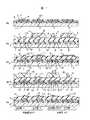
図1は本発明を用いた薄膜トランジスタ基板の製造工程の例をその工程順に示した例である。図は各工程での主要部の断面図である。
【0025】
透光性絶縁基板1、例えば、ガラス基板上に、SiNとSiO2との積層膜からなる下地絶縁膜2を介し、多結晶Siからなる半導体膜3が形成されている。下地絶縁膜2は、基板上に形成する半導体膜を良好に形成する為の層である。このSiNとSiO2との積層膜は、例えばプラズマCVD法(Chemical Vapour Deposition)を用いて形成した。尚、透光性絶縁基板1として、プラスチック基板を目的の応じて用いることが出来る。
【0026】
多結晶Si膜は、プラズマCVDにより堆積したアモルファスSi膜を、パルスエキシマレーザを照射してアニールする方法で形成した。エキシマレーザによるアニールの場合、多結晶Si膜の厚さとしては30nm以上70nm以下が好ましい。更には、40nm以上60nm、より望ましくは50nm程度がよい。30nmより薄い膜では結晶性が低下し、70nmより厚いと結晶化に必要なレーザ光の強度が大きく、むしろ生産性が低下する。又、この場合、結晶化後の凹凸が大きくなり、被覆するゲート絶縁膜が絶縁破壊を起こしやすくなるため適当でない。尚、多結晶Si膜は、スパッタにより堆積したアモルファスSi膜を金属触媒を用いて結晶化する方法、触媒を用いたCVDにより直接堆積する方法など、その他の方法を用いて形成することもできる。
【0027】
50nmの厚さの多結晶Si膜を、ドライエッチを含むホトリソグラフィを用いて、所望形状に加工する。この多結晶Siからなる半導体膜3は、例えば、トランジスタや導体層などを構成する。この後、SiO2からなる第1のゲート絶縁膜4を、TEOS(Tetraethoxysilaneの略称)を用いたプラズマCVDにより50nm堆積した。
【0028】
第1のゲート絶縁膜4は、上記のCVDを用いた方法のほか、450℃以下の温度でオゾンを用いてSi膜を酸化して酸化膜を形成する方法、RF(Radio Frequency)スパッタを用いて酸化膜を堆積する方法、これらを組み合わせた方法など、各種の方法を用いることが出来る。第1のゲート絶縁膜4上に、2wt%のCrを含むMoCr(モリブデン−クロム合金)からなる第1のゲート層を、スパッタにより150nm堆積する。燐酸、硝酸、酢酸、水の混合液を用いたウェットエッチングにより前記MoCr層を所望形状にエッチングする。この結果、端部に約60度の順テーパ形状を有するゲート110及び111が形成される。この状態の主要部の断面図が図1の(a)である。
【0029】
この第1のゲート層からなるゲート110及び111のトランジスタのチャネル方向の両端部をテーパにしておくことは、ソース、ドレインの不純物領域のイオン打込みを良好になすに有用である。即ち、第1のゲート層からなるゲートの上部に絶縁膜6を形成し、この第1のゲート層からなるゲート及び絶縁膜6を介して前記イオン打ち込みを行なう。第1のゲート層からなるゲートの上部に第2のゲート絶縁膜6を形成する際、通例、下部のゲートの端部に対応する位置で第2のゲート絶縁膜6の膜厚が厚く形成される。第2のゲート絶縁膜6の膜厚の変動が、半導体膜に形成される不純物領域の不純物濃度の変動となる。特に、ゲート端部が厚い場合、ソース、ドレインのチャネル端部の不純物濃度が極めて薄くなることも生じ得る。従って、少なくとも、本例のように、第1のゲート層からなるゲートのトランジスタのチャネル方向の両端部をテーパにしておくことが実際的である。
【0030】
又、前記ゲート絶縁膜と下地となるSiO2膜とのエッチング速度の選択比に優れるウェットエッチをゲート加工に用いることで、50nm以下の薄いゲート絶縁膜でも膜がエッチングされるのを抑制できる。
【0031】
更に、SiO2膜の第2のゲート絶縁膜6をTEOSを用いたプラズマCVDにより80nm堆積する。第2のゲート絶縁膜上に、20wt%のWを含むMoW(モリブデン−タングステン合金)からなる第2のゲート層7を厚さ150nm堆積する。ポジレジストを塗布し、露光、現像して、所望形状のレジストパタン8を形成する。燐酸、硝酸、酢酸、水の混合液を用いたウェットエッチングを用いて、第2のゲート層7からなるゲート9をレジストパターン8から1μm後退した幅を有する形状に加工する。わけても、トランジスタのチャネル方向の幅の制御が肝要である。
【0032】
第2のゲート層7を加工するのに用いたレジストパターン8と、第1のゲート層からなるゲート110とをマスクとし、第2のゲート絶縁膜6及び第1のゲート絶縁膜4を通して、半導体膜3に、N型の不純物であるPを注入する。この時、加速電圧70kVにて10の15乗/cm2の濃度である。こうして、ソースおよびドレイン10が形成される。この状態の主要部の断面図が図1の(b)である。
【0033】
尚、第1のゲート膜の膜厚は、このときのPイオンの注入に対して、十分な阻止能力を有する厚さである必要がある。この膜にMoを主成分とする金属膜を用いる場合、厚さは100nm以上が望ましい。
【0034】
前述のレジストパターン8を除去後、第1のゲート層からなるゲート110及び第2のゲート層からなるゲート9をマスクとし、第1のゲート絶縁膜4及び第2のゲート絶縁膜5を通して、Pイオンを加速電圧70kVにてドーズ量10の13乗/cm2で注入する。第2のゲート層からなるゲート9を有する薄膜トランジスタには、ゲート端にPが低濃度で注入され、レジストに覆われていた領域に、LDD11がゲート9に対して自己整合的に形成される。この状態の主要部の断面図が図1の(c)である。
【0035】
一方、第1のゲート層からなるゲート110を有する薄膜トランジスタは、端部にテーパ加工がなされているので、ゲート端に低濃度領域が形成されない。尚、第1のゲート層を加工する際に、端部をテーパ加工する替わりに、ほぼ垂直な形状に加工すると、第1のゲート層からなるゲートを有する薄膜トランジスタに第2のゲート絶縁膜の膜厚に相当するLDD領域を形成することもできる。
【0036】
又、第2のゲート層7からなるゲート9の端部にLDDを自己整合的に形成する方法には、本例のゲートのサイドエッチを用いる方法のほか、レジストアッシングを用いてゲートパタンを縮小させる方法、ゲート端にサイドウォールを形成する方法など他の方法を用いることもできる。
【0037】
次に、先ず、レジストパターン70を形成する。そして、図1(d)に示すように、F(弗素)系ガスを用いたドライエッチを含むホトリソグラフィにより、MoWの第2のゲート層7をドライエッチ加工し、P型TFTのゲート12を形成する。
【0038】
レジストパターン11及び第1のゲート層からなるゲート111をマスクとし、P型の不純物であるB(ボロン)を、第1ゲート絶縁膜4及び第2のゲート絶縁膜6を通して、半導体膜に注入し、P型TFTのソース及びドレイン13を形成する。加速電圧は30kV、ドーズ量は10の15乗/cm2である。この時、N型のTFTとなる領域は、レジストパターン11により保護され、Bが注入されてN型TFTの特性が低下するのが防止される。
【0039】
レジスト膜の除去の後、RTA(Rapid Thermal Anneal)、又は600℃以下の炉アニールによる活性化を行う。
【0040】
以上の工程により、次のような諸トランジスタが同一基板上に形成される。この状態が図1の(e)である。
(1)第1のゲート絶縁膜4と第1のゲート層からなるゲート110を有し、LDDのないNチャネル型の薄膜トランジスタ14。
(2)第1のゲート絶縁膜4と第1のゲート層からなるゲート111を有し、LDDのないPチャネル型の薄膜トランジスタ15。
(3)第1のゲート絶縁膜4及び第2のゲート絶縁膜6と、第2のゲート層からなるゲート9を有し、ゲート端にLDD11が自己整合的に形成されたNチャネル型の薄膜トランジスタ16。
(4)第1のゲート絶縁膜4及び第2のゲート絶縁膜6と、第2のゲート層からなるゲート12を有し、且つゲート端にLDDを持たないP型の薄膜トランジスタ17。
【0041】
N型トランジスタ14、P型トランジスタ15は高駆動力を有するTFT、N型トランジスタ16、P型トランジスタ17は高耐圧なるTFTである。
【0042】
本例では、第1のゲート層をゲートとする薄膜トランジスタと、第2のゲート層をゲートとする薄膜トランジスタのソースおよびドレインが、第1のゲート絶縁膜4及び第2のゲート絶縁膜6を通して半導体膜3に不純物を注入する工程において、それらが同時に形成される。従って、イオン注入工程を増加することなく、ゲート絶縁膜の膜厚の異なる薄膜トランジスタを形成できる。又、第1のゲート層の加工に用いるマスクを除き、ホトリソ工程の増加がない。このように、本方法は、複数の特性を有する薄膜トランジスタを少ない工程数で形成でき、生産性に優れる。又、第2のゲート層を加工するのに用いられるレジストパターン8と、第2のゲート層からなるゲートをマスクとして不純物を注入することにより、自己整合的に形成されたLDDを有し、耐圧に優れる薄膜トランジスタと、LDDを有せず、駆動力に優れる薄膜トランジスタを同時に形成できる利点を有する。
【0043】
本例の要点を述べれば次の通りである。即ち、基板上に、結晶性半導体膜と、第1のゲート絶縁膜と、第1のゲート層と、第2のゲート絶縁膜と、第2のゲート層とが順次積層され、前記第1のゲート絶縁膜と、第1のゲート層からなるゲートとを含む第1の薄膜トランジスタと、前記第1および第2のゲート絶縁膜と、第2のゲート層からなるゲートとを含み、第1のゲート層を含まない第2の薄膜トランジスタとが形成された薄膜トランジスタ基板の製造方法において、第2のゲート層の加工に用いるレジストパターンと、第1のゲート層からなるパターンとをマスクとし、第1及び第2のゲート絶縁膜を通して半導体膜にドーパントを注入する工程を含む薄膜トランジスタ搭載基板の製造方法である。
【0044】
更には、基板上に、結晶性半導体膜と、第1のゲート絶縁膜と、第1のゲート層と、第2のゲート絶縁膜と、第2のゲート層とが順次積層され、前記第1のゲート絶縁膜と、第1のゲート層からなるゲートとを含む第1の薄膜トランジスタと、前記第1および第2のゲート絶縁膜と、第2のゲート層からなるゲートとを含み、第1のゲート層を含まない第2の薄膜トランジスタとが形成された薄膜トランジスタ基板の製造方法において、第2のゲート層をレジストパターンから縮小した形状に加工する工程と、第2のゲート層の加工に用いたレジストパターンおよび第1のゲート層からなるゲートをマスクとして、半導体膜にN型のドーパントを注入する第1の工程と、前記レジストパターンを除去後に第1および第2のゲート層をマスクとし、第1及び第2のゲート絶縁膜を通して前記第1の工程よりも低濃度にN型のドーパントを半導体膜に注入する第2の工程とを含む、薄膜トランジスタ基板の製造方法である。
【0045】
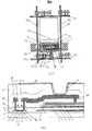
次に、こうした諸TFTを搭載した基板を、透過型の液晶表示装置に用いる薄膜トランジスタ基板として用いる例を説明する。その要点を、図2および図3の断面図を用いて説明する。
【0046】
これまで説明してきた方法によって製造した基板1(図2の(a))の上に、厚さ500nmのSiO2からなる層間絶縁膜18をCVDによって形成する。この後、フッ酸系のウェットエッチを含む通例のホトリソグラフィにより、層間絶縁膜18、第2のゲート絶縁膜6及び第1のゲート絶縁膜4にコンタクトホール71を形成する(図2の(b))。この例に見られるように、本発明においては、ゲート絶縁膜の膜厚の異なる薄膜トランジスタ(14と15、16と17)のソースおよびドレイン10が同1の膜構成4、6、18で覆われている。従って、同1のエッチング工程でコンタクトホールを開口でき、工程数を増加させることがない。尚、トランジスタ14と15とが絶縁膜14をゲート絶縁膜とし、1方、トランジスタ16と17とは絶縁膜4と6とをゲート絶縁膜としている。
【0047】
次いで、配線となるTi/AlSi/Tiの積層膜19を、スパッタにより順次積層したのち、ホトリソグラフィ工程により配線となす。この導体積層膜19は半導体膜3と接続している。尚、この際、第1のゲート層および第2のゲート層への接続もなされる。この導体積層膜19の上下のTi膜は、厚さ100nm、中間のAlSi膜は厚さ500nmとした。この状態が図2の(c))である。
【0048】
次に、図3に表示装置の画素付近の断面を示す。図3にはLDDを有するトランジスタの近傍領域のみを示している。図2(c)で説明したように基板に配線を形成後(図3の(a))、この上部に、プラズマCVDを用いてSiNからなる厚さ400nmの保護膜20を形成する。更に、400℃以下の還元性雰囲気化においてアニールし、水素化処理を行う。その後、感光性の有機膜を塗布し、所望の露光、現像した後、焼成し、厚さ2μmの有機保護膜21を形成する(図3の(b))。この有機保護膜21に開口部23が形成されている。
【0049】
この有機保護膜21マスクとして、SiN保護膜20をドライエッチ加工して、開口部24を形成する。この開口部24はTi/AlSi/Tiの導体積層膜19への開口部である。配線層へのITO(Indium−Tin−Oxide)からなる透明導電膜をスパッタにより堆積し、通例のホトリソグラフィによって画素電極22を形成する。図3の(c)は、こうした薄膜トランジスタ搭載基板の断面図である。
【0050】
又、図1から図3の工程において、半導体膜3、第1のゲート絶縁膜4、第1のゲート層5、第2のゲート絶縁膜6、第2のゲート層7が順次積層された容量30を形成できる。
【0051】
図4は本発明による薄膜トランジスタ基板の製造方法の別な例である。図では図1と同一部位は同一の符号で示した。図1の工程と同様に、厚さ50nmの多結晶Si膜からなる半導体膜3上に、厚さ100nmの第1のゲート絶縁膜4と、Moからなる厚さ150nmの第1のゲート層が順次積層されている。第1のゲート絶縁膜4はTEOSを用いたプラズマCVDにより形成され、Mo層はスパッタにより堆積された。
【0052】
Cl系ガスを用いたドライエッチを含むホトリソグラフィにより、Mo膜を順テーパ加工してゲート5とする。この状態が図4の(a)である。
【0053】
次に、図4(b)に示すように、厚さ50nmのCVD酸化膜からなる第2のゲート絶縁膜6が形成され、その上にスパッタにより、厚さ30nmのTi42と厚さ150nmのMoW合金41の2層膜7が形成される。この導体層の2層膜7は、後に第2のゲート層9となる層である。この上部に、所望形状のフォトレジスト8を形成し、第2のゲート層のMoW合金層41を、燐酸、硝酸、酢酸、水の混合液を用いて、ウェットエッチングする。この場合、MoW合金層41のチャネル方向の幅は、レジスト膜8のチャネル方向の幅から約0.5μm後退した形状に形成する。その後、F系ガスを用いたドライエッチ加工により、Ti膜42をレジストパターンにほぼ同一形状に加工する。この状態が図4の(b)に示される。
【0054】
レジストパターン8および第1のゲート層5をマスクとし、第1ゲート絶縁膜4および第2のゲート絶縁膜6を通してイオン注入を行い、N型の薄膜トランジスタのソースおよびドレイン10を形成する。この際、Pイオンを10の15乗/cm2のドーズ量で、加速電圧80kVで注入する。尚、第1のゲート絶縁膜4と第2のゲート絶縁膜6の厚さの和が150nmより大きい場合、ゲート絶縁膜を通して、半導体膜3にPイオンを注入する際に、レジスト膜8が損傷を受けるため適当でない。
【0055】
レジスト膜8を除去し、第2のゲート層のMoW層41と第1のゲート層5をマスクとし、第1のゲート絶縁膜4及び第2のゲート絶縁膜6を通して、Pイオンを、加速電圧80kVでドーズ量を10の14乗/cm2注入する。このイオン注入によって、ゲート9の端部のTi層42下部の半導体膜3に、低濃度N型領域43が形成された、ゲートオーバーラップ構造の薄膜トランジスタが得られる。ゲートオーバーラップ構造とすることにより、LDDのない薄膜トランジスタと同様の高駆動力を有し、且つ劣化の少ない薄膜トランジスタを形成できる。この状態が図4の(c)である。
【0056】
以下、図1の工程と同様に、こうして準備した基板の上部に、フォトレジスト70を所望形状に形成する。そして、P型TFTのゲート12をドライエッチ加工する。この状態が図4の(d)である。次いで、ゲート5およびレジスト70をマスクとして、Bイオンを注入してP型の薄膜トランジスタを形成する。こうして、異なる特性の薄膜トランジスタが形成された薄膜トランジスタ搭載基板を得ることが出来る。この状態が図4の(e)である。
【0057】
尚、第1のゲート層を2層として同様にゲートオーバーラップ構造の薄膜トランジスタとすることもできる。又、第2層のゲートを加工する際、第2のゲート絶縁膜の一部又は全部をゲート又はゲート加工に用いたレジストをマスクとしてエッチングし、膜厚を減少することもできる。ゲート絶縁膜の膜厚を減少することにより、イオン注入に必要な加速電圧を低減でき、レジストへのダメージを低減できる。この場合も、第1のゲート層をゲートとする薄膜トランジスタと、第2のゲート層をゲートとする薄膜トランジスタにおいて、半導体膜を被覆するゲート絶縁膜の厚さが同一となるため、イオン注入の回数を増やすことがない。
【0058】
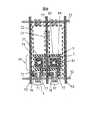
次に、回路内蔵型液晶表示装置の薄膜トランジスタ基板の例を説明する。図5は、回路内蔵型液晶表示装置の薄膜トランジスタ基板における、主要部材の平面配置の概略を示す図である。
【0059】
透光性の絶縁性基板1に、互いに交差する複数の走査信号線51と映像信号線52が配置され、この走査信号線51と映像信号線52との各交差部付近に、画素53が形成されている。画素内の回路は、基本的に表示部材101、保持容量102、スイッチ素子103を含む。図には基本構成を示すが、これらの諸例の詳細は後述される。画素53が形成された領域の周辺に、走査信号線を駆動する駆動回路54と、映像信号線を駆動する駆動回路55が形成されている。更に、外部からの信号を映像信号に変換するインターフェース回路56が形成される。インターフェース回路56には第1のゲート層をゲートとする、高駆動力の薄膜トランジスタを用いて、低電圧駆動を行う。駆動電圧は、例えば10V以下である。1方、走査信号線駆動回路54、映像信号線駆動回路55および画素には、比較的高い電圧が要求されるため、第2のゲート層をゲートとする薄膜トランジスタを用いて形成されている。ここで要請される電圧は、例えば15V以上である。
【0060】
本発明によれば、これまでの説明で明らかなように、低電圧駆動が可能で微細化が容易な薄膜トランジスタを用いた駆動回路と、耐圧に優れた薄膜トランジスタを用いた駆動回路および画素を同1基板上に低コストで形成できる。尚、液晶表示装置に限らず、有機発光素子を用いた表示装置においても、同様の駆動回路の構成とすることで、低消費電力で省面積の駆動回路が形成された表示装置を簡便に形成できる。
【0061】
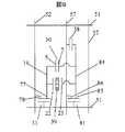
図6の(a)は本発明による液晶表示装置の画素の例を示す平面図、図6の(b)はその断面図である。液晶表示装置では、薄膜トランジスタが形成された基板と向かい合う形で対向基板を設け、基板間に液晶を封入する構造となっているが、図では薄膜トランジスタが形成された基板のみ示した。走査信号線51と映像信号線52に囲まれた画素内に、液晶に電圧を印加する画素電極22がITO透明導電膜により形成されている。画素電極22は図6の(a)では点線で囲まれた領域により表される。画素電極22上に液晶が封入され、画素電極22はスルーホール74を介して映像信号線52と同層の導電膜からなる配線19に接続され、配線19は第2のゲート層からなるゲート31−1及び31−2を備え、ゲート端にLDD11が形成された高耐圧の薄膜トランジスタである画素スイッチ31のソース77に接続される。尚、当該画素スイッチ31は、いわゆるダブルゲート型の薄膜トランジスタであり、走査信号線51に接続されたゲート31−1及び31−2が図示されている。ダブルゲート型の薄膜トランジスタは、単一のゲートを有する薄膜トランジスタに比べ、耐圧の向上とオフ電流の低減を図ることができ、画素スイッチに適している。画素スイッチ31のドレイン78には映像信号線52が接続される。又、画素電極22には電圧を保持する機能をもつ保持容量30が接続されている。保持容量30は、図6の(b)に示す断面図のように、半導体膜3と第1のゲート層5との間に第1のゲート絶縁膜を介した容量と、第1のゲート層5と第2のゲート層7との間に第2のゲート絶縁膜6を介して形成された容量の並列接続により形成される。保持容量の下層電極をなす半導体膜3は画素スイッチ30のソースより延伸され、又、第2のゲート層7は配線19を通しコンタクトホール73を介してやはり画素スイッチのソース30に接続される。一方、保持容量の電極をなす第1のゲート層5は、第1のゲート層と同層の導電膜からなるコモン線32に接続されている。コモン線32と半導体層3の間には下層の半導体膜3が空乏化しないよう、10V以上の電圧が常時印加される。走査信号線からの電圧により、画素スイッチがオンすると、映像信号線からの電圧が画素電極22及び保持容量30に印加される。画素スイッチがオフになると、保持容量30に書き込まれた電圧が画素電極22に印加される電圧を保持する。保持容量の大きさは画素電極の電圧を一定に保つため、画素スイッチのオフ電流による電圧変動が十分小さくなるように設定される。
【0062】
図7の(a)及び図7の(b)は、比較のために示した従来の液晶表示装置の画素の例である。図6の例と同様に、薄膜トランジスタが形成された基板のみ示した。透明電極からなる画素電極22は保持容量30に接続され、保持容量30は画素電極に印加された電圧を保持する機能を有する。図7の(b)に示すように、保持容量30は、半導体膜3とゲート層33との間にゲート絶縁膜34を介して形成された容量と、ゲート層33と配線19との間に層間絶縁膜18を介して形成された容量の並列接続からなるが、層間絶縁膜が厚いため主に半導体膜3とゲート層33との間の容量からなる。保持容量の電極をなすゲート層33は、同層の導電膜からなるコモン線32に接続される。又、保持容量の電極をなし、映像信号線と同層の導電膜からなる配線19は、スルーホール74を介して画素電極22に接続され、他方画素スイッチ31をなすLDD11を有したダブルゲート型の薄膜トランジスタ31のソース77に接続される。ソース77は又保持容量の下層電極をなす半導体膜3に延伸され接続されている。画素スイッチ31をなす薄膜トランジスタのゲート31−1及び31−2はゲート層33と同様の導電膜からなっており、同じくゲート層33と同層の導電膜からなる走査信号線51に接続される。画素スイッチをなす薄膜トランジスタ31は、周辺回路を形成する薄膜トランジスタと同一に比較的薄い単一層からなるゲート絶縁膜34を有しており、オフ電流が大きいために保持容量の面積を大きくとる必要があり、保持容量は画素面積の約30%を占めている。一方、図6の本発明においては、半導体膜3とゲート層との間の容量に加えて、第1のゲート層と第2のゲート層との間の薄い第2のゲート層を介した容量を用いることで面積辺りの容量を増加しており、保持容量30に必要な面積を縮小し、開口率を増加できる利点がある。図6の例において、従来方式のほぼ2倍の面積あたりの容量を持つ保持容量が形成出来る。従って、保持容量の占める面積が約半分に削減され、開口率が約10%増加した。
【0063】
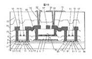
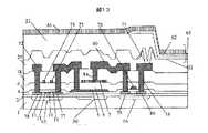
図8、図9、図10は、それぞれ本発明による横電界型の液晶表示装置の画素部分の平面図、回路図および断面図の例である。本例では、保持容量30が、当該画素部の電子回路を構成するトランジスタを構成する絶縁膜を用いて構成される点が重要であるので、この点を先ず説明する。
【0064】
図10の断面図において、第1のゲート層5から延在する導電体層と第2のゲート層7から延在する導電体層の間に、第2のゲート絶縁膜6から延在する絶縁物層を介して保持容量30が形成されている。保持容量30はITOからなる画素電極22と対向電極23の間に接続され、各電極間の電位差を保持する機能を有する。横電界型の液晶表示装置では駆動電圧が比較的高いため、120nm以上の比較的厚いゲート絶縁膜を有する薄膜トランジスタを画素スイッチに用いる。1方、本発明により、周辺回路には100nm以下のより薄いゲート絶縁膜を有する低消費電力な駆動回路を簡便に形成できる。
【0065】
図9に画素部の等価回路を示す。画素電極22と対向電極23の間の電界により液晶59を駆動する。画素電極22と対向電極23との間には、本発明による第1のゲート層と第2のゲート層の間に形成された保持容量30が接続され、液晶に印加される電圧を保持する。画素電極22と対向電極23はそれぞれ画素スイッチ31、81に接続される。画素スイッチ31、81は走査信号線51の電圧によりオンとなり、それぞれ映像信号線52と画素電極22、及び対向電圧信号線57と対向電極23を接続し、保持容量30に電圧を書き込んだのちオフとなる。保持容量に保持される電圧は、液晶の劣化を防ぐため、1定の周期で逆向きに印加される。従来用いられている、半導体膜を電極に用いた容量では電圧の向きによって空乏化し容量が変動するため、図9の構成は適当でない。本発明の容量は半導体膜を用いなくても十分な容量が得られるため、図9の構成を用いて従来必要であった容量のための走査信号線に平行な配線を省略でき、開口率を増加できる利点を有する。
【0066】
更に、図8の平面図の構成とすれば、対向電極と対向電圧信号線を重ねることで開口率を増加できる。尚、重ねることで図9に示す寄生容量58が発生し、対向電極の電位が対向電圧信号線の電位により変動するが、液晶59に印加される電圧は保持容量30により保たれるため、表示が変動することはない。
【0067】
横電界型の液晶表示装置においても、薄膜トランジスタが形成された基板と対向電極との間に液晶を封入した構造を用いるが、図では薄膜トランジスタが形成された基板のみ示した。図8の22及び23の点線で囲んだ領域が、それぞれITO透明電極で形成された画素電極との対向電極を示す。画素電極22はスルーホール74を介し、映像信号線52と同層の導電膜からなる配線19に接続され、配線19はコンタクトホール73を介して保持容量30の下層電極をなす第1のゲート層5に接続されている。配線19は、第1の画素スイッチ31をなす薄膜トランジスタのソース77にも接続されている。一方、対向電極23はスルーホール83を介して映像信号線と同層の導電膜からなる配線84に接続され、配線84はコンタクトホール82を介して保持容量30の上層電極をなす第2のゲート層7に接続され、又第2の画素スイッチ81をなす薄膜トランジスタのソース85にも接続される。画素スイッチ31はソース77とドレイン78の間の半導体膜3上に、ゲートを兼ねる走査信号線51が2回横断する形状とすることで、2つのゲートを有するいわゆるダブルゲート型の薄膜トランジスタとしている。
【0068】
薄膜トランジスタ31は走査信号線51からなるゲートの両端に、それぞれLDD11が形成された高耐圧の薄膜トランジスタとしている。薄膜トランジスタ81も同様にLDDを有するダブルゲート型の薄膜トランジスタである。
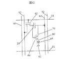
【0069】
図11、図12、図13は、それぞれ本発明による有機発光素子を用いた表示装置の画素部付近の平面図、回路図、及び断面図の例である。
【0070】
平行に並ぶ映像信号線52と電源線57、およびそれらに交差する走査信号線51がそれぞれ複数配置され、各交差部付近に画素が形成されている。画素内には、走査信号線51をゲートに、映像信号線52および保持容量30にソースおよびドレインが接続された薄膜トランジスタ63と、IZO(Indium−Zinc−Oxide)等の透明電極で構成される画素電極22に接続された薄膜トランジスタ64が形成されている。画素電極上には、有機保護膜21の開口部に、ホール輸送層、発光層、電子伝達層がマスクを用いた蒸着により画素ごとに異なった波長の発光特性を持つように堆積され、さらに全面にAlからなる対向電極65が蒸着されて有機発光素子65が形成されている。画素電極に接続された薄膜トランジスタのゲートには、ゲート電圧を保持する保持容量30が接続される。
【0071】
図11において、有機発光素子65の下層電極をなす画素電極22は破線内部の領域で示される。画素電極22はスルーホール74を介し、映像信号線52と同層な導電膜からなる配線19に接続され、配線19を介してLDDを持たない高駆動力のP型の薄膜トランジスタ64のドレイン80に接続される。一方、薄膜トランジスタ80のソースは、映像信号線と同層な導電膜からなる電源線60に接続されている。又、薄膜トランジスタ80のゲート76は、保持容量30の下層電極をなす第1のゲート層5に延伸され、さらにN型の薄膜トランジスタ63のソース77に接続される。一方、保持容量30の上層電極をなす、第2のゲート層と同層な導電膜7は、電源線60に接続される。薄膜トランジスタ63は、第2のゲート層からなるゲート75を有し、ゲート端にLDD11が形成された高耐圧のダブルゲート型の薄膜トランジスタであり、ゲート75は同層の導電膜からなる走査信号線51に接続されている。又、薄膜トランジスタ63のドレイン77は映像信号線52に接続されている。保持容量30は、薄膜トランジスタ63が走査信号線51からの電圧によりオンされた時に、映像信号線52から印加された電圧が書き込まれ、薄膜トランジスタ63がオフになった時に、その電圧を保持する。保持された電圧は薄膜トランジスタ64のゲートに印加され、薄膜トランジスタ64が画素電極22を介して有機発光素子65に流す電流を制御し、その発光量が所望の値に保持される。従って、保持容量30は、映像の画素での発光量に対応する信号を保持する機能を有している。
【0072】
画素電極に接続された薄膜トランジスタ64には、第1のゲート絶縁膜を介して半導体膜に積層された、第1のゲート層をゲートとする、P型の低しきい値の薄膜トランジスタを用いている。保持容量にソース又はドレインを接続した薄膜トランジスタ63には、第1および第2のゲート絶縁膜を介して半導体膜上に形成された第2のゲート層をゲートとし、ゲート端にLDDが形成された、オフ電流の少ないN型の薄膜トランジスタを用いている。ゲート絶縁膜のより薄い薄膜トランジスタを有機発光素子の駆動に用いると、しきい値変動が小さいため、画素間のばらつきが低減される。保持容量は第1のゲート層と第2のゲート層の間に第2のゲート絶縁膜を介して形成された容量により構成されている。面積あたりの容量の大きい第2のゲート絶縁膜を用いており、保持容量の占める面積を低減して開口率を拡大できる。開口率の増大により、同じ輝度での有機発光素子に流す電流の面密度を低減して劣化を低減し、又発光効率を改善できる利点を有する。又、保持容量は半導体膜を電極に用いない構成としており、薄膜トランジスタのしきい値付近の電圧で生じる半導体膜の空乏化による応答速度の低下や容量の変動がなく、より正確な電圧制御が行え、画質が向上する。尚、薄膜トランジスタの電流バラツキを低減するための補償回路を有する画素においても、駆動に用いる薄膜トランジスタのゲート電圧を保持する機能を有する容量に、本発明の半導体膜を含まない2つのゲート層間の容量を用いることで、開口率と電圧制御性を向上でき、高画質で長寿命の表示素子が得られる利点を有する。
【0073】
以上、実施の諸形態をもって詳細に説明したように、本発明により、低消費電力で省スペースの駆動回路を内蔵した、高画質の液晶表示装置および有機発光素子を用いた表示装置を、生産性よく製造できる。
【0074】
【発明の効果】
本発明の第1の形態によれば、LDD構造を有し、例えば液晶の駆動に適した高耐圧な薄膜トランジスタと、低電圧駆動可能な高駆動力の薄膜トランジスタとを、同1基板上に形成する簡便な製造方法を提供することが出来る。
【0075】
本発明の別な形態によれば、多結晶Si膜を用いた駆動回路内蔵表示装置において、容量の面積を縮小し、高開口率で低消費電力の表示装置を提供することが出来る。
【図面の簡単な説明】
【図1】 図1は本発明による薄膜トランジスタ基板の製造工程の例を示す断面図である。
【図2】 図2は本発明による薄膜トランジスタ基板の製造の例の一部工程を示す断面図である。
【図3】 図3は、本発明による薄膜トランジスタ基板の画素の断面図の例である。
【図4】 図4は、本発明による薄膜トランジスタ基板の製造工程の例を示す断面図である。
【図5】 図5は、本発明による駆動回路内蔵液晶表示装置の例である。
【図6】 図6は、本発明による液晶表示装置の画素の例を示す図である。
【図7】 図7は、従来技術による液晶表示装置の画素の例を示す図である。
【図8】 図8は、本発明による横電界型液晶表示装置の画素の例を示す平面図である。
【図9】 図9は、本発明による横電界型液晶表示装置の画素の例を示す回路図である。
【図10】 図10は、本発明による横電界型液晶表示装置の画素の例を示す断面図である。
【図11】 図11は、本発明による有機発光素子表示装置の画素の例を示す平面図である。
【図12】 図12は、本発明による有機発光素子表示装置の画素の例を示す回路図である。
【図13】 図13は、本発明による有機発光素子表示装置の画素の例を示す断面図である。
【符号の説明】
1:ガラス基板、2:下地膜、3:半導体膜、4:第1のゲート絶縁膜、5:第1のゲート層、6:第2のゲート絶縁膜、7:第2のゲート層、8:レジスト、9:ゲート、10:ソース又はドレイン、11:LDD、12:ゲート、13:ソース又はドレイン、14:TFT、15:TFT、16:TFT、17:TFT、18:層間絶縁膜、19:配線、20:SiN保護膜、21:有機保護膜、22:画素電極、23:開口部、24:開口部、30:保持容量、31:画素スイッチ、32:コモン線、33:ゲート層、34:ゲート絶縁膜、
41:MoW層、42:Ti層、43:低濃度領域、51:走査信号線、52:映像信号線、53:画素、54:走査信号線駆動回路、55:映像信号線駆動回路、56:インターフェース回路、57:対向電圧信号線、58:寄生容量、59:液晶、60電源線、61:対向電極、62:有機導電膜−発光層、63:TFT、64:TFT、65:有機発光素子、70:フォトレジスト、71:コンタクトホール、73:コンタクトホール、74:スルーホール、75:ゲート、76:ゲート、77:ソース、78:ドレイン、79:ソース、80:ドレイン、81:TFT、82:コンタクトホール、83:スルーホール、84:配線、85:ソース、86:ドレイン、101表示部材、102:保持容量、103:スイッチ素子、110:ゲート、111:ゲート。[0001]
BACKGROUND OF THE INVENTION
The present invention relates to a thin film transistor substrate that can be used in a display device with a built-in driving circuit using a polycrystalline Si (silicon) thin film, and a method for manufacturing the same.
[0002]
INDUSTRIAL APPLICABILITY The present invention is useful for a thin film transistor substrate used in a liquid crystal display device or a display device using an organic light emitting element, particularly a liquid crystal display device with a built-in drive circuit using a low-temperature polycrystalline Si technology.
[0003]
[Prior art]
In a liquid crystal display device, a drive circuit using a thin film transistor (hereinafter abbreviated as TFT) is formed on a substrate for the purpose of high definition and low cost. A polycrystalline Si film (hereinafter simply referred to as a low-temperature polycrystalline Si film) formed at a low temperature is used as a base material of the TFT. In particular, a small liquid crystal display device used for a portable information terminal is required to reduce a drive circuit area and reduce power consumption.
[0004]
Many technologies have been proposed for these problems, but they are roughly divided into two aspects. One is a method of forming a high breakdown voltage thin film transistor necessary for driving a liquid crystal and a thin film transistor having a high driving force for a driving circuit on the same substrate, and the second is a configuration of the electronic circuit for the display device. This is an attempt to use a thin film transistor using a low-temperature polycrystalline Si film. As a method for forming a high breakdown voltage thin film transistor necessary for driving a liquid crystal and a thin film transistor having a high driving force for a driving circuit on the same substrate, there is, for example, Japanese Patent Application Laid-Open No. 5-335573. In particular, in an N-type thin film transistor, an LDD (Lightly Doped Drain) which is a low-concentration doped region is provided at the gate end for the purpose of reducing withstand voltage and off-current. An example of a method of forming an LDD in a self-aligned manner without misalignment with the gate end can be found in, for example, Japanese Patent Laid-Open No. 11-163366. An example of a display element in which an organic light emitting element is driven by a thin film transistor using a low-temperature polycrystalline Si film can be found in, for example, ASIA DISPLAY / IDW'01 Proceedings, p319.
[0005]
[Problems to be solved by the invention]
The following problems were found in the conventional TFTs used in the present invention. That is, since a plurality of transistor portions are formed, it is necessary to inject the dopant into the semiconductor film through the gate insulating films having different thicknesses. In this process, the dopant implantation depth is naturally different for gate insulating films having different thicknesses. Therefore, in order to form impurity regions having different implantation depths, it is necessary to perform implantation a plurality of times by adjusting the acceleration voltage. Thus, the number of manufacturing steps increases. On the other hand, in the method of forming a gate insulating film after doping a semiconductor film in advance, an increase in the number of steps can be suppressed, but misalignment is likely to occur between the gate and the doping region. For this reason, there is a difficulty in increasing the parasitic capacitance to the transistor.
[0006]
In addition, in order to form a high-breakdown-voltage thin film transistor with LDD and a high-driving thin film transistor without LDD on the same substrate, a mask for making the LDD is necessary, which increases the number of processes.
[0007]
Against this background, a first object of the present invention is to provide an LDD structure, for example, a high breakdown voltage thin film transistor suitable for driving a liquid crystal and a thin film transistor having a high driving capability capable of low voltage drive. An object of the present invention is to provide a simple production method to be formed on top.
[0008]
Further, in a display device using a thin film transistor using a polycrystalline Si film, since the off-state current of the transistor is large, it is necessary to increase a capacity for holding an image signal. For this reason, there is a problem that the aperture ratio cannot be increased. Another object of the present invention is to provide a display device with a high aperture ratio and low power consumption in a display device with a built-in drive circuit using a polycrystalline Si film, with a reduced capacitance area. In order to serve this purpose, the present invention provides a thin film transistor substrate having a higher aperture ratio than before.
[0009]
[Means for Solving the Problems]
A first aspect of the present invention is to form an impurity region of a thin film transistor having a high breakdown voltage and a high driving force with different gate insulating film thickness by implanting a dopant through two gate insulating films having the same film thickness. Manufacturing method. A second aspect of the present invention is to reduce the occupation area by using an extended portion of one layer of an insulating film constituting a thin film transistor used in a display device.
[0010]
The gist of the present invention is described as follows. That is, the crystalline semiconductor on the substratefilmA first thin film transistor in which a gate made of a first gate layer is stacked, and the crystalline semiconductorfilmA thin film transistor substrate on which the first gate insulating film, the second gate insulating film, and a gate made of a second gate layer are stacked, and a second thin film transistor not including the first gate layer is formed thereon Using a resist pattern used for processing the second gate layer and a pattern made of the first gate layer as a mask, and including a step of implanting a dopant into the semiconductor film through the first and second gate insulating films It is characterized by that.
[0011]
The second aspect of the present invention will be described as follows. That is, the second gate layer is processed into a reduced shape from the resist pattern, and the resist pattern used for processing the second gate layer and the gate made of the first gate layer are used as a mask to form an N-type semiconductor film. And the first and second gate layers as a mask after removing the resist pattern and passing through the first and second gate insulating films at a lower concentration than in the first step. And a second step of injecting a type dopant into the semiconductor film.
[0012]
The main aspects of the present invention are listed as follows.
[0013]
The first aspect of the present invention is (1) on the top of the substrate,pluralCrystalline semiconductorMembraneForming step,
(2) The plurality of crystalline semiconductorsMembraneA step of covering and forming a first insulating film;
(3) The first insulating filmOn top of the first gate layerForming a process,
(4)The first gate layer is formed of a firstNA process to process the gate of the transistor,
(5) Then, second insulation on top of the substrateMembraneForming step,
(6) The second insulating filmSecond gate on topForming a layer;
(7)The second gate layer includes a second gate layer that does not include the first gate layer.NA process to process the gate of the transistor,
(8)Crystalline semiconductor for forming an N-type transistorOn the membraneN-type impurities are implanted through the first insulating film and the second insulating film,First and secondN type transitionsOfProcess for forming impurity regionsAboutThin film transistor withGroupIt is a manufacturing method of a board.
[0014]
In the second embodiment of the present invention, (1) an upper part of a substrate,pluralCrystalline semiconductorMembraneForming step,
(2) The plurality of crystalline semiconductorsMembraneA step of covering and forming a first insulating film;
(3) The first insulating filmA first gate layer comprising a first gate layer on the layer;N-type transistorGateas well asFirstP-type transistorThe gateForming step,
(4) Next, a second insulation is formed on the substrate.MembraneForming step,
(5) The second insulating filmUpInSecond gate layerForming a process,
(6)The second gate layer is formed by using a resist pattern to reduce the second gate layer smaller than the resist pattern.Process to process the gate of N-type transistor,
(7) The above1st andSecondNIn the semiconductor region corresponding to the type transistor,The firstNThe gate of the transistor,The secondNType transistorGateThe resist pattern to be processedThrough the first insulating film and the second insulating film, using as a mask regionAt the first concentrationA step of implanting an N-type impurity, and a first step of the N-type transistor.IncongruityForming a pure region,
(8)The secondNIn the semiconductor region corresponding to the type transistor, the second regionNA second concentration lower than the first concentration through the first insulating film and the second insulating film using the gate of the type transistor as a mask regionNA step of implanting a type impurity,NForming a second impurity region of the type transistor;
(9)Second gate layerTheSecondP-type transistorOn the gateProcess to process,
(10) The crystalline semiconductor constituting the P-type transistorOn the membrane, the firstPA gate of the type transistor and the second transistorPUsing the gate region of the type transistor as a mask region,A step of injecting a P-type impurity through the first insulating film and the second insulating film, and the P-type transistorIncongruityForming a pure region,HaveAnd
The first gameLayerTheGateAnd having the first insulating film as a gate insulating filmSaidA first N-type thin film transistor, a first P-type thin film transistor, and the second gate;LayerTheGateA stack of the first insulating film and the second insulating film as a gate insulating filmAsHaveNot including the first gate layerIt is a manufacturing method of a thin film transistor substrate for forming a second N-type thin film transistor and a second P-type thin film transistor.
[0015]
Here, the N-type transistorOfThe step of forming the impurity regions preferably takes the following means.
[0016]
That is, the said process comprises the said crystalline semiconductor which comprises an N-type transistorOn the membraneIn contrast, the firstNType transistorGameToAndThe secondNCorresponding to the type transistorNType transistor gateUsing the larger region as a mask region, at least the first insulationMembraneAnd implanting an N-type impurity at a first impurity concentration through the second insulating film, and the crystalline semiconductor film constituting the N-type transistor with respect to the first semiconductor filmNType transistorA gate and the secondNType transistorGameAndAnd a step of implanting an N-type impurity at a second impurity concentration lower than the first impurity concentration through the first insulating film and the second insulating film, using as a mask region. The
[0017]
The secondNType transistor gateThe mask region corresponding to the second regionN-type transistor gateIn order to secure an area larger than the area ofN-type transistor gateIt is practical to use a photoresist for processing. In this case, the second is greater than the width of the photoresist.N-type transistor gateA desired shape can be obtained by so-called under-etching so that the width of the film becomes smaller.
[0018]
When the thin film transistor mounting substrate is used in a display device, it is advantageous that the substrate is a translucent insulating substrate. Examples of such a display device include a liquid crystal display device and an organic light emitting device. In addition to a transmissive liquid crystal display device, it can also be used in a reflective liquid crystal display device. A reflective display device can be used even if the substrate is not transparent. In addition, according to the present invention, a thin film transistor that can be driven at a high voltage can be formed together with a peripheral circuit that can be driven at a low voltage. It can also be used.
[0019]
In addition, the secondGate layerMay be a laminate of a plurality of conductor layers.
[0020]
In order to form the first and second impurity regions of the semiconductor device as desired, the film thickness of the first insulating film is the first gate.LayerIt is preferable that the thickness is smaller than the thickness of the film. Further, the sum of the thicknesses of the first and second insulating films is the second gate.LayerIt is preferable that the thickness is smaller than the thickness of the film.
[0021]
A more realistic game that satisfies the above relationshipsLayerAn example of the thickness of the insulating film is as follows. That is, the first gameLayerThe film thickness of the first insulating film and the second insulating film in the region where the N-type impurity and the P-type impurity are implanted is 150 nm or less. Is.
[0022]
In addition, the firstN-type transistorGameGIt is practical that the end is formed in a forward tapered shape. When an insulating layer is formed on top of this and ion implantation is performed through this insulating film, the implanted impurity concentration is reduced by the gate of the insulating film.EndIt is hard to be affected by the thickness variation in the vicinity of the part.
With the above-described configuration of the present invention, dopant implantation into the source and drain of thin film transistors having different thicknesses of the gate insulating film is the same.oneIn addition, the LDD can be separately formed without increasing the number of masks.
[0023]
A thin film transistor mounting substrate used in a typical display device has the following basic configuration. That is, on the insulating substrate, a plurality of first wirings and a plurality of second wirings arranged to cross each other, pixels provided in the vicinity of the intersections of the first wirings and the second wirings, It has at least a capacitor for holding a signal, a switch portion for the pixel, and a drive circuit portion for driving the device. In this case, the switch unit includes a first transistor having a gate insulating film including a stack of a first insulating film and a second insulating film as in the present invention, and the drive circuit unit includes In the case where the second transistor having the first insulating film as the gate insulating film is provided, the capacitor for holding the signal is formed through the second insulating film extending from the gate insulating film. Is extremely useful. In the present invention, a capacitor that includes a capacitor formed between the first gate layer and the second gate layer via the second gate insulating film and holds a video signal applied to the pixel electrode. It is characterized by forming. With this structure, the area occupied by the capacitor in the pixel can be reduced, the aperture ratio can be improved, and the power consumption of the display device can be reduced.
[0024]
DETAILED DESCRIPTION OF THE INVENTION
FIG. 1 shows an example of a manufacturing process of a thin film transistor substrate using the present invention in the order of the processes. The figure is a cross-sectional view of the main part in each step.
[0025]
On a translucent
[0026]
The polycrystalline Si film was formed by a method in which an amorphous Si film deposited by plasma CVD was annealed by irradiation with a pulsed excimer laser. In the case of annealing by excimer laser, the thickness of the polycrystalline Si film is preferably 30 nm or more and 70 nm or less. Furthermore, 40 nm or more and 60 nm, and more desirably about 50 nm is preferable. When the film is thinner than 30 nm, the crystallinity is lowered. When the film is thicker than 70 nm, the intensity of the laser beam necessary for crystallization is increased, and the productivity is rather lowered. Further, in this case, the unevenness after crystallization becomes large, and the gate insulating film to be covered tends to cause dielectric breakdown, which is not appropriate. The polycrystalline Si film can also be formed by other methods such as a method of crystallizing an amorphous Si film deposited by sputtering using a metal catalyst, a method of directly depositing by CVD using a catalyst, and the like.
[0027]
A polycrystalline Si film having a thickness of 50 nm is processed into a desired shape by using photolithography including dry etching. The
[0028]
For the first
[0029]
This first
[0030]
The gate insulating film and the underlying SiO2By using wet etching, which has an excellent etching rate selectivity with respect to the film, for gate processing, it is possible to suppress etching of the film even with a thin gate insulating film of 50 nm or less.
[0031]
Furthermore, SiO2A second
[0032]
A resist pattern 8 used for processing the
[0033]
The first gatefilmIt is necessary that the film thickness be sufficient to prevent the P ion implantation at this time. When a metal film mainly composed of Mo is used for this film, the thickness is desirably 100 nm or more.
[0034]
After removing the resist pattern 8, the first gateLayered gate 110And second gateLayered gate 9Is used as a mask, and P ions are passed through the first
[0035]
oneOn the other hand, the gate consisting of the first gate layer110Since a thin film transistor having a taper process at an end portion, a low concentration region is not formed at a gate end. When the first gate layer is processed, if the end portion is processed into a substantially vertical shape instead of being tapered, the second gate insulating film is formed on the thin film transistor having the gate formed of the first gate layer. An LDD region corresponding to the thickness can also be formed.
[0036]
In addition to the method using the side etching of the gate in this example, the gate pattern is reduced by using resist ashing as a method for forming the LDD in the end portion of the
[0037]
Next, first, a resist
[0038]
Resist
[0039]
After removing the resist film, activation is performed by RTA (Rapid Thermal Anneal) or furnace annealing at 600 ° C. or lower.
[0040]
Through the above steps, the following transistors areoneFormed on a substrate. This state is shown in FIG.
(1) First
(2) First
(3) A gate composed of the first
(4) A gate composed of the first
[0041]
The N-
[0042]
In this example, the first gate layer isAndThe thin film transistor to be connected to the second gate layer.AndThe source and drain of the thin film transistor to be formed are simultaneously formed in the step of injecting impurities into the
[0043]
The main points of this example are as follows. That is, a crystalline semiconductor film, a first gate insulating film, a first gate layer, a second gate insulating film, and a second gate layer are sequentially stacked on the substrate, A first thin film transistor including a gate insulating film, a gate formed of a first gate layer, the first and second gate insulating films, and a gate formed of a second gate layer; In the method of manufacturing a thin film transistor substrate in which a second thin film transistor not including a layer is formed, a resist pattern used for processing the second gate layer and a pattern formed of the first gate layer are used as masks. 2 is a method of manufacturing a thin film transistor mounting substrate including a step of injecting a dopant into a semiconductor film through two gate insulating films.
[0044]
Furthermore, a crystalline semiconductor film, a first gate insulating film, a first gate layer, a second gate insulating film, and a second gate layer are sequentially stacked on the substrate, A first thin film transistor including a gate insulating film, a gate formed of a first gate layer, the first and second gate insulating films, and a gate formed of a second gate layer. In a method of manufacturing a thin film transistor substrate on which a second thin film transistor not including a gate layer is formed, a step of processing the second gate layer into a reduced shape from a resist pattern, and a resist used for processing the second gate layer A first step of implanting an N-type dopant into the semiconductor film using the gate formed of the pattern and the first gate layer as a mask, and using the first and second gate layers as a mask after removing the resist pattern , Than the through the first and second gate insulating film a first step and a second step of implanting N-type dopant into the semiconductor film in a low concentration, a method of manufacturing a thin film transistor substrate.
[0045]
Next, an example will be described in which a substrate on which such TFTs are mounted is used as a thin film transistor substrate used in a transmissive liquid crystal display device. The main points will be described with reference to the cross-sectional views of FIGS.
[0046]
On the substrate 1 (FIG. 2 (a)) manufactured by the method described so far, SiOnm having a thickness of 500 nm.2An
[0047]
Next, a Ti / AlSi / Ti laminated
[0048]
Next, FIG. 3 shows a cross section near the pixel of the display device. FIG. 3 shows only the vicinity of the transistor having the LDD. As described with reference to FIG. 2C, after the wiring is formed on the substrate (FIG. 3A), the
[0049]
Using this organic
[0050]
1 to 3, the capacitance in which the
[0051]
FIG. 4 shows another example of a method of manufacturing a thin film transistor substrate according to the present invention. In the figure, the same as FIG.oneSame partoneThis is indicated by the symbol. Similar to the process of FIG. 1, a semiconductor composed of a polycrystalline Si film having a thickness of 50 nmfilm3, a first
[0052]
The Mo film is forward-tapered to form the
[0053]
Next, as shown in FIG. 4B, a second
[0054]
Using resist pattern 8 and
[0055]
The resist film 8 is removed, and the PW ions are accelerated through the first
[0056]
Thereafter, as in the step of FIG. 1, a
[0057]
Note that a thin film transistor having a gate overlap structure can be formed by using two first gate layers. When processing the gate of the second layer, the second gate insulating filmoneThe film thickness can also be reduced by etching using part or all of the resist as a mask, or a resist used for gate processing. By reducing the thickness of the gate insulating film, the acceleration voltage required for ion implantation can be reduced and damage to the resist can be reduced. Also in this case, in the thin film transistor having the first gate layer as a gate and the thin film transistor having the second gate layer as a gate,filmThe thickness of the gate insulating film coveringoneTherefore, the number of ion implantations is not increased.
[0058]
Next, an example of a thin film transistor substrate of a circuit built-in type liquid crystal display device will be described. FIG. 5 is a diagram showing an outline of a planar arrangement of main members in a thin film transistor substrate of a circuit built-in type liquid crystal display device.
[0059]
A plurality of
[0060]
According to the present invention, as is apparent from the above description, a driving circuit using a thin film transistor that can be driven at a low voltage and can be easily miniaturized, and a driving circuit and a pixel using a thin film transistor having excellent breakdown voltage are the same. It can be formed on the substrate at low cost. In addition, not only in a liquid crystal display device but also in a display device using an organic light emitting element, a display device with a low power consumption and area saving drive circuit can be easily formed by adopting the same drive circuit configuration. it can.
[0061]
6A is a plan view showing an example of a pixel of the liquid crystal display device according to the present invention, and FIG. 6B is a cross-sectional view thereof. In the liquid crystal display device, a counter substrate is provided so as to face a substrate on which a thin film transistor is formed, and liquid crystal is sealed between the substrates. However, only the substrate on which the thin film transistor is formed is shown in the drawing. In the pixel surrounded by the
[0062]
FIG. 7A and FIG. 7B are examples of pixels of a conventional liquid crystal display device shown for comparison. As in the example of FIG. 6, only the substrate on which the thin film transistor is formed is shown. The
[0063]
8, FIG. 9, and FIG. 10 are examples of a plan view, a circuit diagram, and a cross-sectional view of a pixel portion of a horizontal electric field type liquid crystal display device according to the present invention, respectively. In this example, the
[0064]
In the cross-sectional view of FIG. 10, the insulation extending from the second
[0065]
FIG. 9 shows an equivalent circuit of the pixel portion. The
[0066]
Furthermore, with the configuration of the plan view of FIG. 8, the aperture ratio can be increased by overlapping the counter electrode and the counter voltage signal line. 9 is generated, and the potential of the counter electrode varies depending on the potential of the counter voltage signal line, but the voltage applied to the
[0067]
In a horizontal electric field type liquid crystal display device, a structure in which liquid crystal is sealed between a substrate on which a thin film transistor is formed and a counter electrode is used, but only the substrate on which the thin film transistor is formed is shown in the drawing. Regions surrounded by dotted
[0068]
The
[0069]
11, FIG. 12, and FIG. 13 are examples of a plan view, a circuit diagram, and a cross-sectional view in the vicinity of a pixel portion of a display device using an organic light emitting element according to the present invention.
[0070]
A plurality of
[0071]
In FIG. 11, the
[0072]
As the
[0073]
As described above in detail with reference to the embodiments, the present invention provides a high-quality liquid crystal display device incorporating a low-power consumption and space-saving drive circuit and a display device using an organic light-emitting element. Can be manufactured well.
[0074]
【The invention's effect】
According to the first embodiment of the present invention, a high-breakdown-voltage thin film transistor having an LDD structure and suitable for driving a liquid crystal, for example, and a high-driving thin film transistor that can be driven at a low voltage are formed on the same substrate. A simple manufacturing method can be provided.
[0075]
According to another embodiment of the present invention, in a display device with a built-in drive circuit using a polycrystalline Si film, a capacitance area can be reduced, and a display device with high aperture ratio and low power consumption can be provided.
[Brief description of the drawings]
FIG. 1 is a cross-sectional view showing an example of a manufacturing process of a thin film transistor substrate according to the present invention.
FIG. 2 shows an example of manufacturing a thin film transistor substrate according to the present invention.oneIt is sectional drawing which shows a partial process.
FIG. 3 is an example of a cross-sectional view of a pixel of a thin film transistor substrate according to the present invention.
FIG. 4 is a cross-sectional view showing an example of a manufacturing process of a thin film transistor substrate according to the present invention.
FIG. 5 is an example of a liquid crystal display device with a built-in drive circuit according to the present invention.
FIG. 6 is a diagram showing an example of a pixel of a liquid crystal display device according to the present invention.
FIG. 7 is a diagram illustrating an example of a pixel of a liquid crystal display device according to a conventional technique.
FIG. 8 is a plan view showing an example of a pixel of a horizontal electric field type liquid crystal display device according to the present invention.
FIG. 9 is a circuit diagram showing an example of a pixel of a horizontal electric field type liquid crystal display device according to the present invention.
FIG. 10 is a cross-sectional view showing an example of a pixel of a horizontal electric field type liquid crystal display device according to the present invention.
FIG. 11 is a plan view illustrating an example of a pixel of an organic light emitting display device according to the present invention.
FIG. 12 is a circuit diagram illustrating an example of a pixel of an organic light emitting display device according to the present invention.
FIG. 13 is a cross-sectional view illustrating an example of a pixel of an organic light emitting display device according to the present invention.
[Explanation of symbols]
1: glass substrate, 2: base film, 3: semiconductorfilm4: first gate insulating film, 5: first gate layer, 6: second gate insulating film, 7: second gate layer, 8: resist, 9: gate, 10: source or drain, 11 : LDD, 12: gate, 13: source or drain, 14: TFT, 15: TFT, 16: TFT, 17: TFT, 18: interlayer insulating film, 19: wiring, 20: SiN protective film, 21: organic protective film 22: pixel electrode, 23: opening, 24: opening, 30: storage capacitor, 31: pixel switch, 32: common line, 33: gate layer, 34: gate insulating film,
41: MoW layer, 42: Ti layer, 43: low density region, 51: scanning signal line, 52: video signal line, 53: pixel, 54: scanning signal line driving circuit, 55: video signal line driving circuit, 56: Interface circuit, 57: counter voltage signal line, 58: parasitic capacitance, 59: liquid crystal, 60 power supply line, 61: counter electrode, 62: organic conductive film-light emitting layer, 63: TFT, 64: TFT, 65: organic light emitting element 70: Photoresist,71: contact hole,73: contact hole, 74: through hole, 75: gate, 76: gate, 77: source, 78: drain, 79: source, 80: drain, 81: TFT, 82: contact hole, 83: through hole, 84: Wiring, 85: source, 86: drain, 101 display member, 102: holding capacitor, 103: switch element110: Gate 111: Gate.
Claims (15)
Translated fromJapanese前記複数の結晶性半導体膜を覆って第1の絶縁膜を形成する工程、
前記第1の絶縁膜上に第1のゲート層を形成する工程、
前記第1のゲート層を、第1のN型トランジスタのゲートに加工する工程、
次いで、前記基板の上部に第2の絶縁膜を形成する工程、
前記第2の絶縁膜上に導体層からなる第2のゲート層を形成する工程、
前記第2のゲート層上に、第2のN型トランジスタのゲートを覆うレジストパターンを形成する工程、
前記第2のゲート層を、前記レジストパターンを用いて前記レジストパターンより縮小され、かつ、前記第1のゲート層を含まない前記第2のN型トランジスタのゲートに加工する工程、
前記第1及び第2のN型トランジスタに対応する結晶性半導体膜に、前記第1のN型トランジスタのゲートと、前記レジストパターンをマスクとして、前記第1の絶縁膜及び前記第2の絶縁膜とを介して第1の濃度でN型不純物を注入し、第1及び第2のN型トランジスタのソース及びドレインを形成する工程、
次いで、前記レジストパターンを除去し、前記第2のN型トランジスタに対応する前記結晶性半導体膜に、前記第2のN型トランジスタのゲートをマスクとして、前記第1の絶縁膜及び前記第2の絶縁膜とを介して前記第1の濃度より低い第2の濃度でN型不純物を注入することにより、前記第2のN型トランジスタのLDD領域を形成する工程、を有することを特徴とする薄膜トランジスタ基板の製造方法。Forming a plurality of crystalline semiconductor films on the substrate;
Forming a first insulating film covering the plurality of crystalline semiconductor films;
Forming a first gate layer on the first insulating film;
Processing the first gate layer into a gate of a firstN- type transistor;
Then, the step of forming a second insulating film onsaid substrate,
Forming a second gate layer made of a conductor layer on the second insulating film;
Forming a resist pattern covering the gate of the second N-type transistor on the second gate layer;
The second gate layer,the resist pattern by using the is reduced from the resist pattern, and the step of processing the gate ofthe secondN-type transistor that does not includethe first gate layer,
The first insulating film and the second insulating film are formedon the crystalline semiconductor filmscorresponding tothe first and secondN-type transistors using the gate of the first N-type transistor and the resist pattern as a mask. And implanting N-type impuritiesat a first concentration via the first and second N-type transistors to formsources and drains of the first and second N-type transistors,
Next, theresist pattern is removed, and the first insulating film and the second insulating film are formed on the crystalline semiconductor film corresponding to the second N-type transistor using the gate of the second N-type transistor as a mask. A step of forming an LDD region of the second N-type transistor by injecting an N-type impurity at a second concentration lower than the first concentration through an insulating film. A method for manufacturing a substrate.
前記複数の結晶性半導体膜を覆って第1の絶縁膜を形成する工程、
前記第1の絶縁膜上に第1のゲート層を形成する工程、
前記第1のゲート層を第1のN型トランジスタのゲート及び第1のP型トランジスタのゲートに加工する工程、
次いで、前記基板の上部に第2の絶縁膜を形成する工程、
前記第2の絶縁膜上に導体層からなる第2のゲート層を形成する工程、
前記第2のゲート層上に、第2のN型トランジスタのゲート、前記第1のP型トランジスタ及び第2のP型トランジスタを覆う第1のレジストパターンを形成し、前記第1のレジストパターンを用いて、前記第2のゲート層を前記第1のレジストパターンより縮小された第2のN型トランジスタのゲートに加工すると共に、第1のP型トランジスタ及び第2のP型トランジスタを覆うパターンに加工する工程、
前記第1及び第2のN型トランジスタに対応する前記結晶性半導体膜に、前記第1のN型トランジスタのゲート及び前記第1のレジストパターンとをマスクとして、前記第1の絶縁膜及び前記第2の絶縁膜とを介して第1の濃度でN型不純物を注入することにより、前記第1及び第2のN型トランジスタのソース及びドレインを形成する工程、
次いで、前記第1のレジストパターンを除去し、前記第2のN型トランジスタに対応する前記結晶性半導体膜に、前記第2のN型トランジスタのゲートをマスクとして、前記第1の絶縁膜及び前記第2の絶縁膜とを介して前記第1の濃度より低い第2の濃度でN型不純物を注入することにより、前記第2のN型トランジスタのLDD領域を形成する工程、
次いで、前記第2のP型トランジスタのゲート、前記第1及び第2のN型トランジスタを覆う第2のレジストパターンを形成し、前記第2のレジストパターンを用いて、前記第1のP型トランジスタを覆うパターンを除去すると共に、前記第2のP型トランジスタを覆うパターンを前記第2のP型トランジスタのゲートに加工する工程、
前記第1及び第2のP型トランジスタに対応する前記結晶性半導体膜に、前記第1のP型トランジスタのゲート及び第2のレジストパターンをマスクとして、前記第1の絶縁膜及び前記第2の絶縁膜とを介してP型不純物を注入することにより、前記第1及び第2のP型トランジスタのソース及びドレインを形成する工程、
次いで、前記第2のレジストパターンを除去する工程、を有し、
前記第1のゲート層をゲートとし、前記第1の絶縁膜をゲート絶縁膜として有する前記第1のN型薄膜トランジスタ及び前記第1のP型薄膜トランジスタと、前記第2のゲート層をゲートとして、前記第1の絶縁膜と前記第2の絶縁膜の積層をゲート絶縁膜として有する前記第1のゲート層を含まない前記第2のN型薄膜トランジスタ及び前記第2のP型薄膜トランジスタとを形成することを特徴とする薄膜トランジスタ基板の製造方法。Forming a plurality of crystalline semiconductor films on the substrate;
Forming a first insulating film covering the plurality of crystalline semiconductor films;
Forming a first gate layer on the first insulating film;
Processing the first gate layer into a gate of a firstN- type transistor and a gate of a first P-type transistor;
Then, the step of forming a second insulating film onsaid substrate,
Forming a second gate layer made of a conductor layer on the second insulating film;
Forming a first resist pattern covering the gate of the second N-type transistor, the first P-type transistor and the second P-type transistor on the second gate layer, and forming the first resist pattern on the second gate layer; Then, the second gate layer is processed into a gate of a secondN- type transistor reduced in size fromthe first resist pattern, and a pattern covering the first P-type transistor and the second P-type transistor is used. Process to process,
Thecrystalline semiconductor film corresponding to the first and second N-type transistors is masked with the gate of the firstN- type transistor andthe first resist pattern as a mask. Forming asource and a drain of the first and second N-type transistorsby implanting an N-type impurity at a first concentration through the two insulating films;
Then,the first resist pattern is removed, thesaid crystalline semiconductor film corresponding to the secondN-type transistor,a gate of the secondN-type transistor asa mask, the first insulating film And forming anLDD region of the secondN- type transistorby implanting anN- type impurity at a second concentration lower than the first concentration through the second insulating film,
Next, a second resist pattern is formed to cover the gate of the second P-type transistor and the first and second N-type transistors, and the first P-type transistor is formed using the second resist pattern. Removing the pattern covering the gate, and processing thepattern covering the second P-type transistor into the gate of the second P-type transistor;
The crystalline semiconductor filmcorresponding tothe first and second P-type transistors is masked by using the gate of the firstP- type transistor and the secondresist pattern as a mask. Forming asource and a drain ofthe first and second P-type transistorsby implanting P-type impurities through an insulating film;
Next, the step of removing the second resist pattern ,
The first N-type thin film transistor and the first P-type thin film transistor having the first gate layer as a gate and the first insulating film as a gate insulating film, and the second gate layer as a gate, Forming the second N-type thin film transistor and the second P-type thin film transistor not including the first gate layer having a stack of the first insulating film and the second insulating film as a gate insulating film; A method of manufacturing a thin film transistor substrate.
Priority Applications (3)
| Application Number | Priority Date | Filing Date | Title |
|---|---|---|---|
| JP2002134885AJP4084080B2 (en) | 2002-05-10 | 2002-05-10 | Method for manufacturing thin film transistor substrate |
| US10/424,950US6864134B1 (en) | 2002-05-10 | 2003-04-29 | Manufacturing method of thin film transistor substrate |
| US11/032,026US7323716B2 (en) | 2002-05-10 | 2005-01-11 | Manufacturing method of thin film transistor substrate |
Applications Claiming Priority (1)
| Application Number | Priority Date | Filing Date | Title |
|---|---|---|---|
| JP2002134885AJP4084080B2 (en) | 2002-05-10 | 2002-05-10 | Method for manufacturing thin film transistor substrate |
Publications (3)
| Publication Number | Publication Date |
|---|---|
| JP2003332581A JP2003332581A (en) | 2003-11-21 |
| JP2003332581A5 JP2003332581A5 (en) | 2005-09-22 |
| JP4084080B2true JP4084080B2 (en) | 2008-04-30 |
Family
ID=29697353
Family Applications (1)
| Application Number | Title | Priority Date | Filing Date |
|---|---|---|---|
| JP2002134885AExpired - Fee RelatedJP4084080B2 (en) | 2002-05-10 | 2002-05-10 | Method for manufacturing thin film transistor substrate |
Country Status (2)
| Country | Link |
|---|---|
| US (2) | US6864134B1 (en) |
| JP (1) | JP4084080B2 (en) |
Families Citing this family (27)
| Publication number | Priority date | Publication date | Assignee | Title |
|---|---|---|---|---|
| JP4638115B2 (en)* | 2002-07-05 | 2011-02-23 | シャープ株式会社 | Method for manufacturing thin film transistor device |
| JP4030885B2 (en)* | 2003-01-27 | 2008-01-09 | シャープ株式会社 | Method for manufacturing thin film transistor substrate |
| JP3991883B2 (en)* | 2003-02-20 | 2007-10-17 | 日本電気株式会社 | Method for manufacturing thin film transistor substrate |
| JP4467901B2 (en)* | 2003-03-28 | 2010-05-26 | シャープ株式会社 | Method for manufacturing thin film transistor device |
| JP4419119B2 (en)* | 2003-12-03 | 2010-02-24 | 日本電気株式会社 | Electro-optical device and projection display device |
| JP4447304B2 (en)* | 2003-12-22 | 2010-04-07 | 株式会社半導体エネルギー研究所 | Semiconductor device and manufacturing method thereof |
| JP4447305B2 (en)* | 2003-12-22 | 2010-04-07 | 株式会社半導体エネルギー研究所 | Semiconductor device and manufacturing method thereof |
| JP4444035B2 (en)* | 2004-04-21 | 2010-03-31 | シャープ株式会社 | Active matrix substrate for display device and manufacturing method thereof |
| TWI246199B (en)* | 2004-07-09 | 2005-12-21 | Au Optronics Corp | Semiconductor device and LTPS-TFT within and method of making the semiconductor device |
| JP4884660B2 (en)* | 2004-08-11 | 2012-02-29 | シャープ株式会社 | Method for manufacturing thin film transistor device |
| JP4872197B2 (en)* | 2004-08-25 | 2012-02-08 | カシオ計算機株式会社 | Thin film transistor panel and manufacturing method thereof |
| JP2006332400A (en) | 2005-05-27 | 2006-12-07 | Nec Corp | Thin film semiconductor device and manufacturing method thereof |
| EP1793266B1 (en)* | 2005-12-05 | 2017-03-08 | Semiconductor Energy Laboratory Co., Ltd. | Transflective Liquid Crystal Display with a Horizontal Electric Field Configuration |
| KR101226444B1 (en)* | 2005-12-21 | 2013-01-28 | 삼성디스플레이 주식회사 | Method of manufacturing display substrate and display substrate |
| US7719030B2 (en)* | 2006-03-29 | 2010-05-18 | International Rectifier Corporation | Aluminum alloys for low resistance, ohmic contacts to III-nitride or compound semiconductor |
| EP1843194A1 (en) | 2006-04-06 | 2007-10-10 | Semiconductor Energy Laboratory Co., Ltd. | Liquid crystal display device, semiconductor device, and electronic appliance |
| TWI545380B (en) | 2006-05-16 | 2016-08-11 | 半導體能源研究所股份有限公司 | Liquid crystal display device and semiconductor device |
| US7847904B2 (en)* | 2006-06-02 | 2010-12-07 | Semiconductor Energy Laboratory Co., Ltd. | Liquid crystal display device and electronic appliance |
| DE102006060734B4 (en)* | 2006-06-30 | 2014-03-06 | Lg Display Co., Ltd. | Liquid crystal display and method for its production |
| JP4300247B2 (en)* | 2007-12-04 | 2009-07-22 | シャープ株式会社 | Method for manufacturing thin film transistor device |
| JP5491833B2 (en)* | 2008-12-05 | 2014-05-14 | 株式会社半導体エネルギー研究所 | Semiconductor device |
| CN101710586B (en)* | 2009-01-09 | 2011-12-28 | 深超光电(深圳)有限公司 | Storage capacitor for improving aperture opening ratio and manufacturing method thereof |
| KR101481399B1 (en) | 2009-12-18 | 2015-01-14 | 가부시키가이샤 한도오따이 에네루기 켄큐쇼 | Semiconductor device |
| US10121928B2 (en) | 2014-07-01 | 2018-11-06 | Sensl Technologies Ltd. | Semiconductor photomultiplier and a process of manufacturing a photomultiplier microcell |
| US10902769B2 (en)* | 2017-07-12 | 2021-01-26 | Facebook Technologies, Llc | Multi-layer fabrication for pixels with calibration compensation |
| KR102468144B1 (en) | 2018-09-03 | 2022-11-16 | 엘지디스플레이 주식회사 | Display device |
| JP7635545B2 (en)* | 2020-12-18 | 2025-02-26 | セイコーエプソン株式会社 | Light emitting device and projector |
Family Cites Families (16)
| Publication number | Priority date | Publication date | Assignee | Title |
|---|---|---|---|---|
| JPH0793363B2 (en)* | 1991-09-25 | 1995-10-09 | 株式会社半導体エネルギー研究所 | Semiconductor integrated circuit and manufacturing method thereof |
| JP2666103B2 (en) | 1992-06-03 | 1997-10-22 | カシオ計算機株式会社 | Thin film semiconductor device |
| JP3254007B2 (en)* | 1992-06-09 | 2002-02-04 | 株式会社半導体エネルギー研究所 | Thin film semiconductor device and method for manufacturing the same |
| JPH11163366A (en) | 1997-09-25 | 1999-06-18 | Toshiba Corp | Method for manufacturing thin film transistor |
| JP2001051292A (en)* | 1998-06-12 | 2001-02-23 | Semiconductor Energy Lab Co Ltd | Semiconductor device and semiconductor display device |
| US6489952B1 (en)* | 1998-11-17 | 2002-12-03 | Semiconductor Energy Laboratory Co., Ltd. | Active matrix type semiconductor display device |
| TW518650B (en)* | 1999-04-15 | 2003-01-21 | Semiconductor Energy Lab | Electro-optical device and electronic equipment |
| JP2000305483A (en)* | 1999-04-20 | 2000-11-02 | Toshiba Corp | Active matrix substrate manufacturing method |
| JP4038309B2 (en)* | 1999-09-10 | 2008-01-23 | セイコーエプソン株式会社 | Manufacturing method of semiconductor device and manufacturing method of active matrix substrate |
| US6706544B2 (en)* | 2000-04-19 | 2004-03-16 | Semiconductor Energy Laboratory Co., Ltd. | Light emitting device and fabricating method thereof |
| US6781646B2 (en)* | 2000-07-28 | 2004-08-24 | Hitachi, Ltd. | Liquid crystal display device having gate electrode with two conducting layers, one used for self-aligned formation of the TFT semiconductor regions |
| JP4831885B2 (en)* | 2001-04-27 | 2011-12-07 | 株式会社半導体エネルギー研究所 | Method for manufacturing semiconductor device |
| US6506642B1 (en)* | 2001-12-19 | 2003-01-14 | Advanced Micro Devices, Inc. | Removable spacer technique |
| JP2003188183A (en)* | 2001-12-20 | 2003-07-04 | Fujitsu Display Technologies Corp | Thin film transistor device, manufacturing method thereof and liquid crystal display device |
| JP4021194B2 (en)* | 2001-12-28 | 2007-12-12 | シャープ株式会社 | Method for manufacturing thin film transistor device |
| JP3626734B2 (en)* | 2002-03-11 | 2005-03-09 | 日本電気株式会社 | Thin film semiconductor device |
- 2002
- 2002-05-10JPJP2002134885Apatent/JP4084080B2/ennot_activeExpired - Fee Related
- 2003
- 2003-04-29USUS10/424,950patent/US6864134B1/ennot_activeExpired - Lifetime
- 2005
- 2005-01-11USUS11/032,026patent/US7323716B2/ennot_activeExpired - Fee Related
Also Published As
| Publication number | Publication date |
|---|---|
| JP2003332581A (en) | 2003-11-21 |
| US7323716B2 (en) | 2008-01-29 |
| US20050121673A1 (en) | 2005-06-09 |
| US6864134B1 (en) | 2005-03-08 |
Similar Documents
| Publication | Publication Date | Title |
|---|---|---|
| JP4084080B2 (en) | Method for manufacturing thin film transistor substrate | |
| JP3989763B2 (en) | Semiconductor display device | |
| US8288768B2 (en) | Thin film transistor, method of manufacturing the same, and flat panel display device having the same | |
| TWI401802B (en) | Thin film transistor plate and method of manufacturing same | |
| KR100831881B1 (en) | Thin-film semiconductor device | |
| US7642141B2 (en) | Manufacturing method for display device | |
| JP4967631B2 (en) | Display device | |
| KR20070019609A (en) | Exposure mask and manufacturing method of semiconductor device using same | |
| US20030094613A1 (en) | Crystalline silicon thin film transistor panel for OELD and method of fabricating the same | |
| US7348631B2 (en) | Thin film transistor substrate and manufacturing method for the same | |
| KR100566894B1 (en) | Crystalline Silicon TFT Panel and Fabrication Method Using MIC | |
| WO2011004624A1 (en) | Thin-film transistor producing method | |
| JP2006114871A (en) | Semiconductor device and manufacturing method thereof | |
| KR100811997B1 (en) | Thin film transistor and its manufacturing method and flat panel display device including the same | |
| JP4326604B2 (en) | Method for manufacturing semiconductor device | |
| JP4633434B2 (en) | Semiconductor device and manufacturing method thereof | |
| JP2004039997A (en) | Thin film transistor device and method of manufacturing the same, and thin film transistor substrate and display device having the same | |
| JP2011035430A (en) | Method for manufacturing semiconductor device | |
| US8759166B2 (en) | Method for manufacturing thin film transistor device | |
| JP5090693B2 (en) | Display device and manufacturing method thereof | |
| JP4397753B2 (en) | Semiconductor device | |
| JP4197270B2 (en) | Method for manufacturing semiconductor integrated circuit | |
| JP2009210681A (en) | Display and manufacturing method therefor | |
| KR101172015B1 (en) | Thin film transistor plate and method of fabricating the same | |
| KR101123513B1 (en) | TFT and fabrication method thereof |
Legal Events
| Date | Code | Title | Description |
|---|---|---|---|
| A521 | Request for written amendment filed | Free format text:JAPANESE INTERMEDIATE CODE: A523 Effective date:20050419 | |
| A621 | Written request for application examination | Free format text:JAPANESE INTERMEDIATE CODE: A621 Effective date:20050419 | |
| A977 | Report on retrieval | Free format text:JAPANESE INTERMEDIATE CODE: A971007 Effective date:20070420 | |
| A131 | Notification of reasons for refusal | Free format text:JAPANESE INTERMEDIATE CODE: A131 Effective date:20070508 | |
| A521 | Request for written amendment filed | Free format text:JAPANESE INTERMEDIATE CODE: A523 Effective date:20070709 | |
| RD02 | Notification of acceptance of power of attorney | Free format text:JAPANESE INTERMEDIATE CODE: A7422 Effective date:20070709 | |
| A131 | Notification of reasons for refusal | Free format text:JAPANESE INTERMEDIATE CODE: A131 Effective date:20071023 | |
| A521 | Request for written amendment filed | Free format text:JAPANESE INTERMEDIATE CODE: A523 Effective date:20071220 | |
| TRDD | Decision of grant or rejection written | ||
| A01 | Written decision to grant a patent or to grant a registration (utility model) | Free format text:JAPANESE INTERMEDIATE CODE: A01 Effective date:20080122 | |
| A61 | First payment of annual fees (during grant procedure) | Free format text:JAPANESE INTERMEDIATE CODE: A61 Effective date:20080214 | |
| R150 | Certificate of patent or registration of utility model | Free format text:JAPANESE INTERMEDIATE CODE: R150 | |
| FPAY | Renewal fee payment (event date is renewal date of database) | Free format text:PAYMENT UNTIL: 20110222 Year of fee payment:3 | |
| FPAY | Renewal fee payment (event date is renewal date of database) | Free format text:PAYMENT UNTIL: 20110222 Year of fee payment:3 | |
| FPAY | Renewal fee payment (event date is renewal date of database) | Free format text:PAYMENT UNTIL: 20120222 Year of fee payment:4 | |
| LAPS | Cancellation because of no payment of annual fees |