JP4083379B2 - Liquid crystal display device and manufacturing method thereof - Google Patents
Liquid crystal display device and manufacturing method thereofDownload PDFInfo
- Publication number
- JP4083379B2 JP4083379B2JP2000341854AJP2000341854AJP4083379B2JP 4083379 B2JP4083379 B2JP 4083379B2JP 2000341854 AJP2000341854 AJP 2000341854AJP 2000341854 AJP2000341854 AJP 2000341854AJP 4083379 B2JP4083379 B2JP 4083379B2
- Authority
- JP
- Japan
- Prior art keywords
- semiconductor layer
- layer
- liquid crystal
- display device
- crystal display
- Prior art date
- Legal status (The legal status is an assumption and is not a legal conclusion. Google has not performed a legal analysis and makes no representation as to the accuracy of the status listed.)
- Expired - Fee Related
Links
Images


Landscapes
- Liquid Crystal (AREA)
- Devices For Indicating Variable Information By Combining Individual Elements (AREA)
- Thin Film Transistor (AREA)
Description
Translated fromJapanese【0001】
【発明の属する技術分野】
本発明は、チャネルエッチ型の薄膜トランジスタを備えた液晶表示装置及びその製造方法に関する。
【0002】
【従来の技術】
近年、デスクトップ型パソコン向けの15〜23インチ(XGA〜UXGAクラス)の液晶表示装置の普及に伴い、薄膜トランジスタ(TFT:Thin Film Transistor)をスイッチング素子として備えたアクティブマトリクス型液晶表示装置の需要が一層増加している。需要拡大に応じた供給量を確保するために、様々な簡略化プロセス、増産プロセス等が検討されている。
【0003】
同様に、超高精細表示の液晶表示装置の需要も増加している。超高精細表示を実現するにはTFTの小型化と特性の安定性の向上が必要であり、そのためチャネルエッチ型TFTの採用が検討されている。チャネルエッチ型TFTは、ソース/ドレイン電極を形成する際のエッチング時に動作半導体層のチャネル領域を保護するためのチャネル保護膜を有していない。したがって、エッチングレートの変動を考慮すると、チャネル領域上のn型不純物半導体層を残渣なくエッチング除去するには、チャネル領域上面までエッチングする必要がある。
【0004】
アクティブマトリクス型液晶表示装置は、非選択時にオフ状態となって信号を遮断するスイッチング素子を各画素毎に設けることによってクロストークを防止しており、単純マトリクス方式の液晶表示装置と比較して優れた表示特性を有している。特にTFTを用いた液晶表示装置の表示特性は、その駆動能力の高さからCRT(Cathode Ray Tube)にも匹敵する。
【0005】
一般的なTN(Twisted Nematic)型液晶表示装置は、透明絶縁性基板であるアレイ基板と対向基板の間に液晶を封入した構造を有している。両基板の相互に対向する面(対向面)のうち、対向基板側にはコモン(共通)電極、カラーフィルタ及び配向膜等が形成され、アレイ基板側にはTFT、画素電極及び配向膜等が形成されている。両基板の対向面と反対側の面には、各々偏光板が貼り付けられている。この2枚の偏光板の偏光軸を互いに直交するように配置した液晶表示装置は、電圧無印加状態で光を透過し、電圧印加状態で遮光するノーマリホワイトモードとなる。逆に、2枚の偏光板の偏光軸を互いに平行に配置した液晶表示装置はノーマリブラックモードとなる。
【0006】
近年、液晶表示装置のより一層の高性能化、特に高視野角特性、表示品質の向上及び高精細化等が強く要求されている。高視野角特性と表示品質の向上を実現する表示装置として、垂直配向(VA:Vertica1 Alignment)型液晶表示装置、特にMVA(Multi−domain Vartical Alignment)型液晶表示装置が普及しつつある。
【0007】
MVA型液晶表示装置は、アレイ基板と対向基板、及び両基板間に封入された誘電率異方性が負の垂直配向型液晶で構成されている。両基板の対向面のうち、対向基板側にはコモン電極、カラーフィルタ及び垂直配向膜等が形成され、アレイ基板側にはTFT、画素電極及び垂直配向膜等が形成されている。両基板の対向面と反対側の面には、それぞれ偏光板が互いに偏光軸を直交させて配置されている。このMVA型液晶表示装置は垂直配向膜を有しており、電圧無印加状態で液晶が配向膜に対して垂直に配向するのでノーマリブラックモードとなる。アレイ基板側のインジウム酸化スズ(ITO:Indium Tin Oxide)からなる画素電極には、ドメイン規制用のスリットが形成されており、対向基板側にはレジストからなる土手(突起部)が形成されている。アレイ基板側の画素電極と対向基板側のコモン電極との間に充分な電圧を印加すると、垂直配向型の液晶分子はその電界の方向と垂直に配列する。このとき、各スリットを挟んだ両側、あるいは各突起部を挟んだ両側では、液晶分子の配列方向が異なる、いわゆる配向分割(マルチドメイン)が達成される。この状態でアレイ基板側の偏光板に入射した光の一部は、対向基板側の偏光板を通過するため、液晶表示装置は明状態を表示する。各画素毎に印加する電圧を制御することで画素毎の階調表示が得られ、液晶表示装置に所望の画像を表示することが可能となる。また上述の配向分割により斜め方向の光漏れが抑制され、視野角特性が改善される。
【0008】
従来のチャネルエッチ型TFTを有する液晶表示装置のアレイ基板及びその製造方法を図32乃至図42を用いて説明する。まず、従来のチャネルエッチ型TFTを有する液晶表示装置におけるアレイ基板の構成について図32を用いて説明する。図32は、従来のチャネルエッチ型TFTを有する液晶表示装置におけるTFT及び蓄積容量の構成を示す概略断面図である。TFT102は、絶縁性を有する透明ガラス基板106上に形成されたゲート電極108を有している。ゲート電極108上にはゲート絶縁膜110が形成されている。ゲート絶縁膜110上には動作半導体層112が形成されている。動作半導体層112上には、オーミックコンタクト層として機能するn型不純物半導体層116が形成されている。
【0009】
n型不純物半導体層116上には、ソース電極114及びドレイン電極118が形成されている。ソース電極114及びその下層のn型不純物半導体層116と、ドレイン電極118及びその下層のn型不純物半導体層116とは、動作半導体層112のチャネル領域上に設けられた間隙で分離されて、電気的に絶縁されている。また、全面には保護膜120が形成されている。保護膜120上の各画素領域内に広がって画素電極122が形成されている。画素電極122は、ソース電極114上の保護膜120を開口したコンタクトホール124を介してソース電極114に接続されている。
【0010】
蓄積容量104は、透明ガラス基板106上にゲート電極108と同一の形成材料で形成された蓄積容量バスライン126を有している。蓄積容量バスライン126上にはゲート絶縁膜110と同一の形成材料で絶縁膜128が形成されている。絶縁膜128上には、ソース電極114及びドレイン電極118と同一の形成材料で蓄積容量対向電極130が形成されている。蓄積容量対向電極130上には、保護膜120が形成されている。保護膜120上には画素電極122が形成されている。画素電極122は、蓄積容量対向電極130上の保護膜120を開口したコンタクトホール132を介して蓄積容量対向電極130に接続されている。
【0011】
次に、従来のチャネルエッチ型TFTを有する液晶表示装置におけるアレイ基板の製造方法を図33乃至図42を用いて説明する。図33乃至図37は、従来のチャネルエッチ型TFTを有する液晶表示装置におけるTFT及び蓄積容量の製造工程を示す工程断面図である。図38乃至図42は、従来のチャネルエッチ型TFTを有する液晶表示装置におけるアレイ基板の製造工程を示す平面図である。まず、図33及び図38に示すように、絶縁性を有する透明ガラス基板106上全面に導電膜を成膜し、パターニングしてゲート電極108、ゲートバスライン134、ゲート端子136、蓄積容量バスライン126、蓄積容量端子140をそれぞれ形成する。なお、図38に示したゲートバスライン134は、破線に挟まれた領域が図33に示したゲート電極108として機能する。
【0012】
次に、全面にゲート絶縁膜110及びゲート絶縁膜110と同一の形成材料で同時に形成される絶縁膜128と、a−Si層とn+a−Si層とを連続して成膜する。次いで、n+a−Si層とa−Si層をパターニングして、図34及び図39に示すように、動作半導体層112とn型不純物半導体層116を形成する。図39に示すように、動作半導体層112とn型不純物半導体層116は、ゲートバスライン134のゲート電極108上方に形成される。
【0013】
次に、全面に金属層を成膜してパターニングし、図35に示すように、ソース電極114とドレイン電極118と蓄積容量対向電極(中間電極)130とをそれぞれ形成する。同時に、図40に示すように、ドレインバスライン142とドレイン端子144を形成する。上記金属層からソース電極114とドレイン電極118を分離形成すると共に動作半導体層112にチャネル領域を形成するエッチング工程で、金属層及びn型不純物半導体層116は、ゲート電極108直上の動作半導体層112上面で所定の間隙ができるようにエッチングされて分離され、電気的に絶縁される。このエッチング工程では、間隙下の動作半導体層112表面もエッチングされる。これ以降、少なくともn型不純物半導体層116から動作半導体層112表面までのエッチングをチャネルエッチングと言う。
【0014】
次に、全面に透明絶縁膜からなる保護膜120を成膜してパターニングし、図36に示すように、ソース電極114上のコンタクトホール124と、蓄積容量対向電極130上のコンタクトホール132とを形成する。同時に、図41に示すように、ゲート端子136上のコンタクトホール146と、蓄積容量端子140上のコンタクトホール148と、ドレイン端子144上のコンタクトホール150とを形成する。
【0015】
最後に、図37及び図42に示すように、全面にITOからなる透明導電膜を形成してパターニングし、各画素領域内に画素電極122を形成する。また、当該パターニングにより、ゲート端子136上、蓄積容量端子140上、及びドレイン端子144上に保護導電膜152をそれぞれ形成する。以上の工程でアレイ基板が完成する。また、本例に示したMVA型液晶表示装置では、画素電極122を形成する際に、図42に示すようなドメイン規制用のスリット150が形成される。
【0016】
【発明が解決しようとする課題】
従来のチャネルエッチ型TFTの製造方法において、図34に示した工程では、SF6、He、HClの混合ガスを用いた反応性イオンエッチング(RIE)法によるドライエッチングが行われている。エッチングの停止時期は、エッチング中におけるSiF2のプラズマ発光(発光波長:390.2nm)の発光強度の低下に基づくa−Si層(図34の動作半導体層112の形成層)の終点検出(EPD検出:End Point Detecting)により決定される。プラズマ発光強度は、上記発光波長の光強度を検出する受光素子を有し、光強度に応じて信号を出力する光強度センサにより検出される。
【0017】
一方、図35に示したチャネルエッチング工程は、上述と同様にSF6、He、HClの混合ガスによるRIE法を用いている。ところが、a−Si層(図35では動作半導体層112)とその上層に形成されたn+a−Si層(図35ではn型不純物半導体層116)のSiF2のプラズマ発光強度の差はほとんどなく、しかもチャネルエッチング領域の面積が狭いため発光強度は極めて低い。このため、n+a−Si層だけのエッチング終点をEPD検出で得ることは困難である。したがって、チャネルエッチング工程では、エッチング時間を制御してn+a−Si層のエッチングを停止するようにしている。この時間制御によるエッチングでは、チャネル領域上層のn+a−Si層を確実に除去するために、チャネル領域の動作半導体層112の掘り込みマージンを十分確保しておく必要がある。このため、動作半導体層112となるa−Si層の膜厚は120〜200nm以上に厚く形成する必要がある。ところが、このような厚い膜厚にしてしまうとチャネル領域で安定した特性が得られず、また成膜時間とエッチング時間が余分に必要となってしまうという問題が生ずる。
【0018】
また、上記のようなエッチング時間の制御によるチャネルエッチングでは、チャネル領域の動作半導体層112の膜厚をリアルタイムで測定するのは困難であり、エッチング終了後に残膜厚用TEG(例えば、ナノメトリクス社製の膜厚測定装置)等で測定するしかない。また、超高精細表示を実現する小型化されたTFT102では、さらにチャネルエッチング領域の面積が狭くなるためエッチングレートに変動が生じ、時間制御によるエッチングではチャネル領域の動作半導体層112の掘り込み量の変動も大きくなる。したがって、チャネル領域の動作半導体層112の膜厚の均一性が悪化するだけでなく、部分的に極めて薄くなることもあり、TFT102で安定した特性が得られないという問題がある。
【0019】
さらに、TFT102及び蓄積容量104の形成領域以外の領域に形成される、窒化シリコン(SiN)膜等からなる絶縁膜128もチャネルエッチングにおいてプラズマに長時間さらされるためにダメージを受けてしまうという問題もある。
【0020】
本発明の目的は、チャネルエッチングの終点を確実に検出することにより、特性の安定したチャネルエッチ型TFTを有する液晶表示装置及びその製造方法を提供することにある。
【0021】
【課題を解決するための手段】
上記目的は、絶縁性を有する基板上にゲート電極を形成し、前記ゲート電極上にゲート絶縁膜を形成し、前記ゲート絶縁膜上に動作半導体層を形成し、前記動作半導体層上にn型不純物半導体層を形成し、前記n型不純物半導体層上に導電体層を形成し、前記導電体層とn型不純物半導体層とをエッチングして、前記ゲート電極上の前記動作半導体層の上層を露出させて所定の間隙で対向するソース電極及びドレイン電極を形成して薄膜トランジスタを作製し、保護膜を介して前記ソース電極と接続する画素電極を形成する液晶表示装置の製造方法において、前記導電体層とn型不純物半導体層とのエッチングの際に同時にエッチングされるダミー半導体層を前記基板上に形成し、前記ダミー半導体層がエッチング除去されたら前記エッチングを停止することを特徴とする液晶表示装置の製造方法によって達成される。
【0022】
【発明の実施の形態】
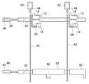
本発明の第1の実施の形態による液晶表示装置及びその製造方法について、図1乃至図16を用いて説明する。まず、本実施の形態による液晶表示装置の概略の構成を図1及び図2を用いて説明する。図1は本実施の形態による液晶表示装置の全体構成を示している。アレイ基板81上には、TFT2と、蓄積容量4と、例えばITO等の透明導電膜からなる画素電極を有する画素領域84とがマトリクス状に多数配置された表示領域86が画定されている。なお、図1では画素領域84内に1画素分の液晶表示装置の等価回路を示している。表示領域の周囲の図中左方にはゲートバスライン駆動回路88が配置され、図中上方にはドレインバスライン駆動回路90が配置されている。
【0023】
また、システム側からのドットクロックや、水平同期信号(Hsync)、垂直同期信号(Vsync)、及びRGBデータが入力する入力端子92が図中パネル上方に設けられている。アレイ基板81は図示しないシール剤を介して対向基板94と対向して貼り合わされている。アレイ基板81と対向基板94との間のセルギャップに液晶lcが封入されている。アレイ基板81上の表示電極と対向基板94上のコモン電極、及びそれらに挟まれた液晶lcで液晶容量Clcが形成されている。一方、アレイ基板側で表示電極と蓄積容量バスラインが形成されて蓄積容量54が形成されている。
【0024】
表示領域86内には図中上下方向に延びるドレインバスライン42が図中左右方向に平行に複数形成されている。複数のドレインバスライン42のそれぞれは、ドレインバスライン駆動回路90に接続されており、ドレインバスライン42毎に所定の階調電圧が印加されるようになっている。
【0025】
また、ドレインバスライン42とほぼ直交する方向に延びるゲートバスライン34が図中上下方向に平行に複数形成されている。複数のゲートバスライン34のそれぞれは、ゲートバスライン駆動回路88に接続されている。ゲートバスライン駆動回路88は、内蔵したシフトレジスタから出力されるビット出力に同期して、複数のゲートバスライン34に対して順にゲートパルスを出力するようになっている。
【0026】
ゲートバスライン駆動回路88により複数のゲートバスライン34のいずれか1つにゲートパルスが出力されると、当該ゲートバスライン34に接続されている複数のTFT2がオン状態になる。これにより、ドレインバスライン駆動回路90から複数のドレインバスライン42のそれぞれに印加されている階調電圧が各画素電極に印加される。
【0027】
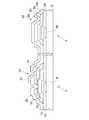
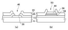
図2は、本実施の形態による液晶表示装置におけるTFT及び蓄積容量の構成を示す概略断面図である。TFT2は、絶縁性を有する透明ガラス基板6上に、例えば膜厚100nmのアルミニウム(Al)層と膜厚50nmの窒化モリブデン(MoN)層とをこの順に積層した金属層により形成されたゲート電極8を有している。ゲート電極8の形成材料は、Al層とチタン(Ti)層とをこの順に積層した金属層や、クロム(Cr)層、Al合金層等であってもよい。ゲート電極8上には、例えば膜厚100〜600nmのSiN膜又は酸化シリコン(SiO)膜によりゲート絶縁膜10が形成されている。ゲート絶縁膜10上には、膜厚10〜270nm(例えば60nm)のa−Si層により動作半導体層12が形成されている。動作半導体層12上には、膜厚5〜50nm(例えば30nm)のn+a−Si層により、オーミックコンタクト層として機能するn型不純物半導体層16が形成されている。
【0028】
n型不純物半導体層16上には、例えば膜厚50nmのMoN層と、膜厚150nmのAl層と、膜厚90nmのMoN層と、膜厚10nmのモリブデン(Mo)層とをこの順に積層した金属層によりソース電極14及びドレイン電極18が形成されている。ソース電極14及びドレイン電極18の形成材料は、膜厚20nmのTi層と膜厚75nmのAl層と膜厚20nmのTi層とをこの順に積層した金属層や、Al合金層、その他の低抵抗金属を積層した金属層等であってもよい。
【0029】
ソース電極14及びその下層のn型不純物半導体層16と、ドレイン電極18及びその下層のn型不純物半導体層16とは、ゲート電極8上方の動作半導体層12上部でエッチングされて分離され、互いに絶縁されている。このエッチングの際の両電極の分離絶縁を確実にするため、動作半導体層12のチャネル領域上表面もエッチングされている。基板全面には、例えば膜厚330nmのSiN膜からなる保護膜20が形成されている。保護膜20上には、例えば膜厚70nmのITOからなる画素電極22が形成されている。画素電極22は、ソース電極14上の保護膜20を開口して形成されたコンタクトホール24を介してソース電極14に接続されている。
【0030】
蓄積容量4は、透明ガラス基板6上にゲート電極8と同一の形成材料で形成された蓄積容量バスライン26を有している。蓄積容量バスライン26上には、ゲート絶縁膜10と同一の形成材料で絶縁膜28が形成されている。絶縁膜28上には、動作半導体層12と同一の形成材料で動作半導体層12より薄い残存層58が形成されている。残存層58上には、ソース電極14及びドレイン電極18と同一の形成材料で蓄積容量対向電極30が形成されている。蓄積容量対向電極30上には、保護膜20が形成されている。保護膜20上にはTFT2のソース電極14に接続されている画素電極22が形成されている。画素電極22は、蓄積容量対向電極30上の保護膜20を開口して形成されたコンタクトホール32を介して蓄積容量対向電極30に接続されている。
【0031】
次に、本実施の形態による液晶表示装置の製造方法を図3乃至図16を用いて説明する。図3乃至図9は、本実施の形態による液晶表示装置におけるTFT及び蓄積容量の製造工程を示す工程断面図であり、図中左側にTFT2を示し、図中右側に蓄積容量4を示している。図10及び図11は、本実施の形態による液晶表示装置におけるゲート端子及びドレイン端子の製造工程を示す工程断面図である。図10及び図11において、(a)はゲート端子36を示しており、(b)はドレイン端子44を示している。図12乃至図16は、本実施の形態による液晶表示装置におけるアレイ基板の製造工程を示す平面図である。
【0032】
まず、透明ガラス基板6全面に、例えばPVD(Physical Vapor Depotion)法により、例えば膜厚100nmのAl層と膜厚50nmのMoN層とをこの順に成膜して金属層(図示せず)を形成する。金属層の形成材料は、この他Al層とTi層との積層による金属層や、Cr層、Al合金層等であってもよい。次に、全面にレジストを塗布してから第1の露光用マスク(図示せず)を用いて露光した後現像して、金属層上に所定のパターンのレジスト膜(図示せず)を形成する。次に、このレジスト膜をエッチングマスクとして、例えばAlエッチャントを用いたウェットエッチングにより金属層をエッチングする。当該エッチングにより、図3に示すゲート電極8と蓄積容量バスライン26を形成する。同時に、図12に示すゲートバスライン34とゲート端子36と蓄積容量端子40を形成する。なお、図12に示したゲートバスライン34は、破線で挟まれた領域で図3に示したゲート電極8として機能する。上記エッチングにおいて、金属層がAl層とTi層とを積層した金属層であれば例えば塩素(Cl)系ガスによりドライエッチングし、Cr層であれば例えばCrエッチャントによりウェットエッチングする。
【0033】
次に、図4に示すように、例えばプラズマCVD法により、透明で絶縁性を有するSiN膜又はSiO膜を膜厚100〜600nm(例えば350nm)に成膜して、ゲート絶縁膜10及び絶縁膜28を全面に形成する。次に、膜厚10〜270nm(例えば60nm)の動作半導体層12を形成するためのa−Siからなる半導体層54を全面に形成する。次に、膜厚5〜50nm(例えば30nm)のn+a−Si層56を全面に形成する。動作半導体層12を形成するための半導体層54は、n+a−Si層56の膜厚に5nmを加算した膜厚以上になるように形成する。
【0034】
次に、全面にレジストを塗布してから、第2の露光用マスク(図示せず)を用いて露光した後現像して、n+a−Si層56上に所定のパターンのレジスト膜(図示せず)を形成する。次に、このレジスト膜をエッチングマスクとして用い、n+a−Si層56と、動作半導体層12を形成するための半導体層54の上層とをRIE法によりドライエッチングする。これにより図5及び図13に示すように、n型不純物半導体層16及び動作半導体層12を形成すると共に、動作半導体層12の形成領域以外の領域にダミー半導体層となる残存層58を形成する。ドライエッチングに用いるエッチングガスは、例えばSF6、He、HClの混合ガスである。このとき、残存層58の膜厚が、n+a−Si層56(図5ではn型不純物半導体層16)の膜厚以上になるようにエッチング時間を制御する。n+a−Si層56の膜厚が例えば30nmであれば、残存層58は膜厚が30〜40nm(例えば33nm)になるように形成する。なお、形成された残存層58の膜厚は、例えば1ロット(例えば基板20枚)のうち1枚乃至数枚の基板に対して、膜厚測定装置等を用いて残存層58の膜厚を測定することにより容易に管理される。
【0035】
次に、例えばPVD法により、例えば膜厚50nmのMoN層と、膜厚150nmのAl層と、膜厚90nmのMoN層と、膜厚10nmのMo層とをこの順に成膜し、図6に示すように金属層60を全面に形成する。金属層60は、膜厚20nmのTi層と膜厚75nmのAl層と膜厚20nmのTi層とをこの順に積層した金属層や、Al合金層、その他の低抵抗金属を積層した金属層等であってもよい。次に、全面にレジストを塗布してから、第3の露光用マスク(図示せず)を用いて露光した後現像して、金属層60上に所定のパターンのレジスト膜(図示せず)を形成する。このレジスト膜をエッチングマスクとして、MoN層とAl層とMoN層とMo層とを積層した金属層60を、例えばAlエッチャントを用いてウェットエッチングする。なお、金属層60がTi層とAl層とTi層とを積層した金属層であれば、例えばCl系ガスによりドライエッチングする。
【0036】
続いてチャネルエッチング工程に移り、動作半導体層12のうちゲート電極8上部に形成されるチャネル領域上のn型不純物半導体層16と、残存層58とをRIE法によるドライエッチングで一括エッチングする。当該一括エッチングにより、図7に示すように、ソース電極14、ドレイン電極18、n型不純物半導体層16及び動作半導体層12が形成される。同時に、図14に示すように、ドレインバスライン42、ドレイン端子44及び蓄積容量対向電極30が形成される。ドライエッチングに用いるエッチングガスは、例えばSF6、He、HClの混合ガスである。このチャネルエッチングの際、全面に形成されている残存層58をダミー半導体層として、a−Siで形成されている残存層58のエッチング時に生ずるSiF2のプラズマ発光(発光波長:390.2nm)の発光強度を検出する。プラズマ発光強度は、上記発光波長の光強度を検出する受光素子を有し、光強度に応じて信号を出力する光強度センサにより検出される。
【0037】
残存層58が全てエッチング除去されるとSiF2のプラズマ発光強度は急激に低下するので、上記光強度センサを用いてプラズマ発光強度の低下をモニタすることで残存層58のエッチングの終点を検出できる。また、残存層58の形成材料であるa−Siのエッチングレートとn型不純物半導体層16の形成材料であるn+a−Siのエッチングレートはほぼ等しい。そこで、残存層58からのプラズマ発光強度の低下により残存層58のエッチングの終点を検出したら、チャネルエッチングを停止させるようにする。n型不純物半導体層16は残存層58の膜厚以下の膜厚に形成されているので、このチャネルエッチングによりチャネル領域上のn型不純物半導体層16を確実にエッチング除去できる。例えば膜厚33nmの残存層58のエッチングの終点がプラズマ発光強度の低下により検出されたら、チャネル領域上の膜厚30nmのn型不純物半導体層16は確実にエッチング除去されており、さらにその下層の動作半導体層12のチャネル領域の上部3nmがエッチング除去されて掘り込まれている。なお図7に示すように、蓄積容量2は絶縁膜28と蓄積容量対向電極30との間に残存層58が挟まれた構造となっている。
【0038】
次に、例えばプラズマCVD法により、透明で絶縁性を有する例えば膜厚330nmのSiN膜を成膜し、保護膜20を全面に形成する。次に、全面にレジストを塗布してから、第4の露光用マスク(図示せず)を用いて露光した後現像して、保護膜20上に所定のパターンのレジスト膜(図示せず)を形成する。次に、このレジスト膜をエッチングマスクとして、ソース電極14上、蓄積容量電極30上及びドレイン端子44上の保護膜20をエッチングする。当該エッチングにより、図8に示すソース電極14上のコンタクトホール24、蓄積容量対向電極30上のコンタクトホール32、及び図10(b)に示すドレイン端子44上のコンタクトホール50を形成する。同時に、ゲート端子36上及び蓄積容量端子40上の保護膜20及びゲート絶縁膜10を一括エッチングする。当該一括エッチングにより、図10(a)に示すゲート端子36上のコンタクトホール46、及び蓄積容量端子40上のコンタクトホール48が形成される(図15参照)。エッチング条件は、例えば8.0Pa、SF6/O2=200/200[sccm]、600WのRIE法によるドライエッチングである。
【0039】
次に、例えばPVD法により、例えば膜厚70nmのITOを成膜し、透明導電膜(図示せず)を全面に形成する。次に、全面にレジストを塗布してから、第5の露光用マスク(図示せず)を用いて露光した後現像して、透明導電膜上に所定のパターンのレジスト膜(図示せず)を形成する。次に、このレジスト膜をエッチングマスクとして、透明導電膜を例えばシュウ酸等を用いてウェットエッチングする。当該ウェットエッチングにより、図9に示す画素電極22と、図11(a)に示すゲート端子36上の保護導電膜52と、蓄積容量端子40上の保護導電膜52と、図11(b)に示すドレイン端子44上の保護導電膜52とをそれぞれ形成する(図16参照)。図16に示した画素電極22には、MVA型液晶表示装置に特有のドメイン規制用のスリット50が形成されている。スリット50により複数の領域に分割された画素電極22は、スリット50上の数ヶ所で導通をとって接続されている。以上説明した工程を経て、本実施の形態による液晶表示装置におけるアレイ基板が完成する。この後、対向基板と貼り合わせ、液晶を封止して本実施の形態による液晶表示装置が完成する。
【0040】
本実施の形態によれば、ダミー半導体層となる残存層58が、TFT2を形成する領域以外の広い領域に形成される。そのため、チャネルエッチングの際、同時にエッチングされる残存層58から生ずるプラズマ発光強度がチャネル領域から生ずるプラズマ発光強度と比較して格段に大きくなるので、その検出は容易に行える。プラズマ発光強度の低下をモニタして残存層58のエッチングの終点を検出し、それに基づいてチャネルエッチングを停止すれば、チャネル領域上のn型不純物半導体層16を容易に正確にエッチング除去できるようになる。したがって、動作半導体層12となるa−Si層の膜厚を120〜200nm以上に厚く形成してチャネル領域の掘り込みマージンを確保しておく必要がないため、チャネル領域で安定した特性を得ることができるとともに、成膜時間とエッチング時間を短縮できるようになる。
【0041】
また、本実施の形態によれば、チャネル領域上のn型不純物半導体層16を容易に正確にエッチング除去できるので、チャネル領域の動作半導体層12を必要以上にエッチング除去してしまうことはない。そのため、時間制御によるエッチングと異なり、チャネル領域の動作半導体層12の膜厚を測定する工程は不必要となる。
【0042】
また、本実施の形態によれば、時間制御によるエッチングと異なり、チャネル領域上のn型不純物半導体層16のエッチング除去が完了した時期を正確に検出できるため、チャネル領域の動作半導体層12を必要以上にエッチング除去してしまうことはない。そのため、超高精細表示を実現する小型化されたTFT2であっても、チャネル領域の動作半導体層12の膜厚を正確に得ることができ、TFT2は均一で安定した特性を得ることができる。
【0043】
さらに、本実施の形態によれば、残存層58の膜厚管理を行っているので、チャネル領域上のn型不純物半導体層16を確実にエッチング除去できる。さらに、CVD法等による成膜の突発的な成膜異常や、RIE法によるエッチングの突発的なエッチング異常等があっても早期に発見することができるので、製造歩留まりの向上に寄与することができる。また、残存層58の膜厚管理を行うことで、動作半導体層12のチャネル領域の掘り込み量をほぼ特定できるため、チャネル領域の掘り込み量とTFT2の特性との相関関係を効率良く管理することが可能となる。さらに、残存層58は基板全面に形成されるため、膜厚測定において測定位置や測定数を任意に決定することができる。
【0044】
また、本実施の形態によれば、TFT2及び蓄積容量4の形成領域以外の領域に形成される絶縁膜28上に残存層58が形成されるため、チャネルエッチングにおいて絶縁膜28がプラズマに長時間さらされることを防いでダメージを受けないようにすることができる。
【0045】
次に、本発明の第2の実施の形態による液晶表示装置及びその製造方法について、図17乃至図31を用いて説明する。まず、本実施の形態による液晶表示装置の概略の構成を図17を用いて説明する。本実施の形態による液晶表示装置の全体構成は、図1に示した第1の実施の形態と同様の構成を有するので、その説明は省略する。
【0046】
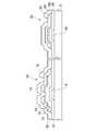
図17は、本実施の形態による液晶表示装置におけるTFT及び蓄積容量の構成を示す概略断面図である。TFT2は、絶縁性を有する透明ガラス基板6上に、例えば膜厚100nmのAl層と膜厚50nmのMoN層とをこの順に積層した金属層により形成されたゲート電極8を有している。ゲート電極8の形成材料は、Al層とTi層とをこの順に積層した金属層や、Cr層、Al合金層等であってもよい。ゲート電極8上には、例えば膜厚100〜600nmのSiN膜又はSiO膜によりゲート絶縁膜10が形成されている。ゲート絶縁膜10上には、膜厚10〜270nm(例えば60nm)のa−Si層により動作半導体層12が形成されている。動作半導体層12上には、膜厚5〜50nm(例えば30nm)のn+a−Si層により、オーミックコンタクト層として機能するn型不純物半導体層16が形成されている。
【0047】
n型不純物半導体層16上には、例えば膜厚50nmのMoN層と、膜厚150nmのAl層と、膜厚90nmのMoN層と、膜厚10nmのMo層とをこの順に積層した金属層によりソース電極14及びドレイン電極18が形成されている。ソース電極14及びドレイン電極18の形成材料は、膜厚20nmのTi層と膜厚75nmのAl層と膜厚20nmのTi層とをこの順に積層した金属層や、Al合金層、その他の低抵抗金属を積層した金属層等であってもよい。
【0048】
ソース電極14及びその下層のn型不純物半導体層16と、ドレイン電極18及びその下層のn型不純物半導体層16とは、ゲート電極8上方の動作半導体層12上部でエッチングされて分離され、互いに絶縁されている。このエッチングの際の両電極の分離絶縁を確実にするため、動作半導体層12のチャネル領域上表面もエッチングされている。基板全面には、例えば膜厚330nmのSiN膜からなる保護膜20が形成されている。保護膜20上には、例えば膜厚70nmのITOからなる画素電極22が形成されている。画素電極22は、ソース電極14上の保護膜20を開口して形成されたコンタクトホール24を介してソース電極14に接続されている。
【0049】
蓄積容量4は、透明ガラス基板6上にゲート電極8と同一の形成材料で形成された蓄積容量バスライン26を有している。蓄積容量バスライン26上には、ゲート絶縁膜10と同一の形成材料で絶縁膜28が形成されている。絶縁膜28上には、動作半導体層12と同一の形成材料で動作半導体層12より薄い残存層58が形成されている。残存層58上には、TFT2のn型不純物半導体層16を形成するn+a−Si層56が形成されている。n+a−Si層56上には、ソース電極14及びドレイン電極18と同一の形成材料で蓄積容量対向電極30が形成されている。蓄積容量対向電極30上には、保護膜20が形成されている。保護膜20上にはTFT2のソース電極14に接続されている画素電極22が形成されている。画素電極22は、蓄積容量対向電極30上の保護膜20を開口して形成されたコンタクトホール32を介して蓄積容量対向電極30に接続されている。
【0050】
次に、本実施の形態による液晶表示装置の製造方法を図18乃至図31を用いて説明する。図18乃至図24は、本実施の形態による液晶表示装置におけるTFT及び蓄積容量の製造工程を示す工程断面図であり、図中左側にTFT2を示し、図中右側に蓄積容量4を示している。図25及び図26は、本実施の形態による液晶表示装置におけるゲート端子及びドレイン端子の製造工程を示す工程断面図である。図25及び図26において、(a)はゲート端子36を示しており、(b)はドレイン端子44を示している。図27乃至図31は、本実施の形態による液晶表示装置におけるアレイ基板の製造工程を示す平面図である。
【0051】
まず、透明ガラス基板6全面に、例えばPVD法により、例えば膜厚100nmのAl層と膜厚50nmのMoN層とをこの順に成膜して金属層(図示せず)を形成する。金属層の形成材料は、この他Al層とTi層との積層による金属層や、Cr層、Al合金層等であってもよい。次に、全面にレジストを塗布してから第1の露光用マスク(図示せず)を用いて露光した後現像して、金属層上に所定のパターンのレジスト膜(図示せず)を形成する。次に、このレジスト膜をエッチングマスクとして、例えばAlエッチャントを用いたウェットエッチングにより金属層をエッチングする。当該エッチングにより、図18に示すゲート電極8と蓄積容量バスライン26を形成する。同時に、図27に示すゲートバスライン34とゲート端子36と蓄積容量端子40を形成する。なお、図27に示したゲートバスライン34は、破線で挟まれた領域で図18に示したゲート電極8として機能する。上記エッチングにおいて、金属層がAl層とTi層とを積層した金属層であれば例えばCl系ガスによりドライエッチングし、Cr層であれば例えばCrエッチャントによりウェットエッチングする。
【0052】
次に、図19に示すように、例えばプラズマCVD法により、透明で絶縁性を有するSiN膜又はSiO膜を膜厚100〜600nm(例えば350nm)に成膜して、ゲート絶縁膜10(絶縁膜28)を全面に形成する。次に、a−Siで膜厚10〜270nm(例えば60nm)の動作半導体層12を形成するための半導体層54を全面に形成する。
【0053】
次に、全面にレジストを塗布してから、第2の露光用マスク(図示せず)を用いて露光した後現像して、動作半導体層12を形成するための半導体層54上に所定のパターンのレジスト膜(図示せず)を形成する。次に、このレジスト膜をエッチングマスクとして用い、動作半導体層12を形成するための半導体層54の上層をRIE法によりドライエッチングする。これにより図20及び図28に示すように、動作半導体層12を形成すると共に、動作半導体層12の形成領域以外の領域にダミー半導体層の一部を構成する残存層58を形成する。ドライエッチングに用いるエッチングガスは、例えばSF6、He、HClの混合ガスである。このとき、残存層58の膜厚が例えば30nmになるようにエッチング時間を制御する。なお、形成された残存層58の膜厚は、例えば1ロット(例えば基板20枚)のうち1枚乃至数枚の基板に対して、膜厚測定装置等を用いて残存層58の膜厚を測定することにより容易に管理される。
【0054】
次に、膜厚5〜50nm(例えば30nm)のn+a−Si層56を全面に形成する。n+a−Si層56の一部は、その下層の残存層58と共にダミー半導体層として機能する。次いでn+a−Si層56上に、例えばPVD法により、例えば膜厚50nmのMoN層と、膜厚150nmのAl層と、膜厚90nmのMoN層と、膜厚10nmのMo層とをこの順に成膜し、図21に示すように金属層60を全面に形成する。金属層60は、膜厚20nmのTi層と膜厚75nmのAl層と膜厚20nmのTi層とをこの順に積層した金属層や、Al合金層、その他の低抵抗金属を積層した金属層等であってもよい。次に、全面にレジストを塗布してから、第3の露光用マスク(図示せず)を用いて露光した後現像して、金属層60上に所定のパターンのレジスト膜(図示せず)を形成する。このレジスト膜をエッチングマスクとして、MoN層とAl層とMoN層とMo層とを積層した金属層60を、例えばAlエッチャントを用いてウェットエッチングする。なお、金属層60がTi層とAl層とTi層とを積層した金属層であれば、例えばCl系ガスによりドライエッチングする。
【0055】
続いてチャネルエッチング工程に移り、動作半導体層12のうちゲート電極8上部に形成されるチャネル領域上のn型不純物半導体層16と、残存層58とをRIE法によるドライエッチングで一括エッチングする。当該一括エッチングにより、図22に示すように、ソース電極14、ドレイン電極18、n型不純物半導体層16及び動作半導体層12が形成される。同時に、図29に示すように、ドレインバスライン42、ドレイン端子44及び蓄積容量対向電極30が形成される。ドライエッチングに用いるエッチングガスは、例えばSF6、He、HClの混合ガスである。このチャネルエッチングの際、全面に形成されている残存層58及びその上層のn+a−Si層56をダミー半導体層として、n+a−Si層56と、a−Siで形成されている残存層58とのエッチング時に生ずるSiF2のプラズマ発光(発光波長:390.2nm)の発光強度を検出する。プラズマ発光強度は、上記発光波長の光強度を検出する受光素子を有し、光強度に応じて信号を出力する光強度センサにより検出される。
【0056】
n+a−Si層56及びその下層の残存層58が全てエッチング除去されるとSiF2のプラズマ発光強度は急激に低下するので、上記光強度センサを用いてプラズマ発光強度の低下をモニタすることで残存層58のエッチングの終点を検出できる。そこで、n+a−Si層56及び残存層58からのプラズマ発光強度の低下により残存層58のエッチングの終点を検出したらチャネルエッチングを終了させるようにする。このチャネルエッチングによりチャネル領域上のn型不純物半導体層16を確実にエッチング除去できる。例えば膜厚30nmのn+a−Si層56と膜厚30nmの残存層58のエッチングの終点が検出されたら、チャネル領域上の膜厚30nmのn型不純物半導体層16は確実にエッチング除去されており、さらにその下層の膜厚60nmの動作半導体層12のチャネル領域の上部30nmがエッチング除去されて掘り込まれている。このように、残存層58の膜厚と、チャネル領域の動作半導体層12の掘り込まれる深さはほぼ同じである。なお図22に示すように、蓄積容量2は、絶縁膜28と蓄積容量対向電極30との間に、残存層58とn+a−Si層56とが挟まれた構造となる。
【0057】
次に、例えばプラズマCVD法により、透明で絶縁性を有する例えば膜厚330nmのSiN膜を成膜し、保護膜20を全面に形成する。次に、全面にレジストを塗布してから、第4の露光用マスク(図示せず)を用いて露光した後現像して、保護膜20上に所定のパターンのレジスト膜(図示せず)を形成する。次に、このレジスト膜をエッチングマスクとして、ソース電極14上、蓄積容量電極30上及びドレイン端子44上の保護膜20をエッチングする。当該エッチングにより、図23に示すソース電極14上のコンタクトホール24、蓄積容量対向電極30上のコンタクトホール32、及び図25(b)に示すドレイン端子44上のコンタクトホール50を形成する。同時に、ゲート端子36上及び蓄積容量端子40上の保護膜20及びゲート絶縁膜10を一括エッチングする。当該一括エッチングにより、図25(a)に示すゲート端子36上のコンタクトホール46、及び蓄積容量端子40上のコンタクトホール48が形成される(図30参照)。エッチング条件は、8.0Pa、SF6/O2=200/200[sccm]、600Wの例えばRIE法によるドライエッチングである。
【0058】
次に、例えばPVD法により、例えば膜厚70nmのITOを成膜し、透明導電膜(図示せず)を全面に形成する。次に、全面にレジストを塗布してから、第5の露光用マスク(図示せず)を用いて露光した後現像して、透明導電膜上に所定のパターンのレジスト膜(図示せず)を形成する。次に、このレジスト膜をエッチングマスクとして、透明導電膜を例えばシュウ酸等を用いてウェットエッチングする。当該ウェットエッチングにより、図24に示す画素電極22と、図26(a)に示すゲート端子36上の保護導電膜52と、蓄積容量端子40上の保護導電膜52と、図26(b)に示すドレイン端子44上の保護導電膜52とをそれぞれ形成する(図31参照)。図31に示した画素電極22には、MVA型液晶表示装置に特有のドメイン規制用のスリット50が形成されている。スリット50により複数の領域に分割された画素電極22は、スリット50上の数ヶ所で導通をとって接続されている。以上説明した工程を経て、本実施の形態による液晶表示装置におけるアレイ基板が完成する。この後、対向基板と貼り合わせ、液晶を封止して本実施の形態による液晶表示装置が完成する。
【0059】
本実施の形態によれば、ダミー半導体層となる残存層58及びその上層のn+a−Si層56が、TFT2を形成する領域以外の広い領域に形成される。そのため、チャネルエッチングの際、同時にエッチングされる残存層58から生ずるプラズマ発光強度がチャネル領域から生ずるプラズマ発光強度と比較して格段に大きくなるので、その検出は容易に行える。プラズマ発光強度の低下をモニタして残存層58のエッチングの終点を検出し、それに基づいてチャネルエッチングを停止すれば、チャネル領域上のn型不純物半導体層16を容易に正確にエッチング除去できるようになる。したがって、動作半導体層12となるa−Si層の膜厚を120〜200nm以上に厚く形成してチャネル領域の掘り込みマージンを確保しておく必要がないため、チャネル領域で安定した特性を得ることができるとともに、成膜時間とエッチング時間を短縮できるようになる。
【0060】
また、本実施の形態によれば、チャネル領域上のn型不純物半導体層16を容易に正確にエッチング除去できるので、チャネル領域の動作半導体層12を必要以上にエッチング除去してしまうことはない。そのため、時間制御によるエッチングと異なり、チャネル領域の動作半導体層12の膜厚を測定する工程は不必要となる。
【0061】
また、本実施の形態によれば、時間制御によるエッチングと異なり、チャネル領域上のn型不純物半導体層16のエッチング除去が完了した時期を正確に検出できるため、チャネル領域の動作半導体層12を必要以上にエッチング除去してしまうことはない。そのため、超高精細表示を実現する小型化されたTFT2であっても、チャネル領域の動作半導体層12の膜厚を正確に得ることができ、TFT2は均一で安定した特性を得ることができる。
【0062】
さらに、本実施の形態によれば、残存層58の膜厚管理を行っているので、チャネル領域上のn型不純物半導体層16を確実にエッチング除去できる。さらに、CVD法等による成膜の突発的な成膜異常や、RIE法によるエッチングの突発的なエッチング異常等があっても早期に発見することができるので、製造歩留まりの向上に寄与することができる。また、残存層58の膜厚管理を行うことで、動作半導体層12のチャネル領域の掘り込み量をほぼ特定できるため、チャネル領域の掘り込み量とTFT2の特性との相関関係を効率良く管理することが可能となる。さらに、残存層58は基板全面に形成されるため、膜厚測定において測定位置や測定数を任意に決定することができる。
【0063】
また、本実施の形態によれば、TFT2及び蓄積容量4の形成領域以外の領域に形成される絶縁膜28上に残存層58が形成されるため、チャネルエッチングにおいて絶縁膜28がプラズマに長時間さらされることを防いでダメージを受けないようにすることができる。
【0064】
本発明は、上記実施の形態に限らず種々の変形が可能である。
例えば、上記実施の形態においては、MVA型液晶表示装置を例に挙げて説明したが、本発明はこれに限らず、TFTを備えたTN型液晶表示装置やIPS(In−plane Switching)型液晶表示装置等にも適用可能である。
【0065】
また、上記実施の形態においては、TFTを備えた液晶表示装置を例に挙げて説明したが、本発明はこれに限らず、TFTを備えたEL(Electroluminescence)表示装置等にも適用可能である。
【0066】
さらに、上記実施の形態においては、ダミー半導体層から生ずるSiF2のプラズマ発光強度の低下をモニタしてチャネルエッチングの終点を検出しているが、本発明はこれに限らず、プラズマ発光強度の種々の変動をモニタしてチャネルエッチングを制御するようにしてもよい。
【0067】
また、上記実施の形態においては、動作半導体層12がa−Siにより形成されているTFTを有する液晶表示装置を例に挙げて説明したが、本発明はこれに限らず、動作半導体層12がp−Si(ポリシリコン)により形成されているTFTを有する液晶表示装置にも適用できる。
【0068】
さらに、上記第2の実施の形態においては、ダミー半導体層が残存層58とn+a−Si層56とで構成されているが、本発明はこれに限らず、ダミー半導体層はn+a−Si層56のみで構成されていてもよい。ダミー半導体層のn+a−Si層56と、チャネル領域上のn型不純物半導体層16は、同一層であるのでほぼ同じ膜厚を有しており、チャネルエッチングの際にエッチング除去される時期はほぼ同時である。したがって、ダミー半導体層のn+a−Si層56の下層に残存層58を形成しなくてもチャネルエッチングの終点を検出することは可能である。残存層58を形成しない場合の蓄積容量2は、絶縁膜28と蓄積容量対向電極30との間に、n型不純物半導体層16の形成材料で形成されたn+a−Si層56が挟まれた構造となっている。
【0069】
なお、上記実施の形態による液晶表示装置は、一方の電極となる蓄積容量バスラインと、誘電体となる絶縁膜と、他方の電極となる蓄積容量対向電極とを備えた蓄積容量が、絶縁膜と蓄積容量対向電極との間に半導体層を有していることを特徴としている。半導体層は、動作半導体層の形成材料、n型不純物半導体層の形成材料、又は動作半導体層の形成材料とn型不純物半導体層の形成材料との積層により形成されている。蓄積容量対向電極の三積層構造については、本出願人による先願に係る特開平06−202153号公報に開示されている。また、n型不純物半導体層とソース/ドレイン電極を形成する金属層とを連続して成膜して、その後一括でソース/ドレイン電極とチャネル領域を形成することは、本出願人による先願に係る特開昭58−112366号公報に開示されており、本発明はそれらの代替、応用、あるいは発展技術と言うこともできる。
【0070】
以上説明した実施の形態に基づき、本発明は以下のようにまとめられる。
(付記1)
絶縁性を有する基板上にゲート電極を形成し、前記ゲート電極上にゲート絶縁膜を形成し、前記ゲート絶縁膜上に動作半導体層を形成し、前記動作半導体層上にn型不純物半導体層を形成し、前記n型不純物半導体層上に導電体層を形成し、前記導電体層とn型不純物半導体層とをエッチングして、前記ゲート電極上の前記動作半導体層の上層を露出させて所定の間隙で対向するソース電極及びドレイン電極を形成して薄膜トランジスタを作製し、保護膜を介して前記ソース電極と接続する画素電極を形成する液晶表示装置の製造方法において、
前記導電体層とn型不純物半導体層とのエッチングの際に同時にエッチングされるダミー半導体層を前記基板上に形成すること
を特徴とする液晶表示装置の製造方法。
【0071】
(付記2)
付記1記載の液晶表示装置の製造方法において、
前記エッチングは、前記ダミー半導体層から生ずるプラズマ発光の発光強度の変化を検出して停止させること
を特徴とする液晶表示装置の製造方法。
【0072】
(付記3)
付記1又は2に記載の液晶表示装置の製造方法において、
前記ダミー半導体層は、前記動作半導体層を形成するための半導体層を全面に形成し、前記動作半導体層の形成領域以外の領域の前記半導体層の上層をエッチング除去した残存層で形成されること
を特徴とする液晶表示装置の製造方法。
【0073】
(付記4)
付記3記載の液晶表示装置の製造方法において、
前記ダミー半導体層は、前記n型不純物半導体層の膜厚以上で前記動作半導体層の膜厚以下の膜厚に形成されること
を特徴とする液晶表示装置の製造方法。
【0074】
(付記5)
付記3又は4に記載の液晶表示装置の製造方法において、
前記n型不純物半導体層は、5nm以上で50nm以下の膜厚に形成され、
前記動作半導体層は、前記n型不純物半導体層の膜厚に5nmを加算した膜厚以上で270nm以下の膜厚に形成されること
を特徴とする液晶表示装置の製造方法。
【0075】
(付記6)
付記1又は2に記載の液晶表示装置の製造方法において、
前記ダミー半導体層は、前記動作半導体層を形成するための半導体層を全面に形成し、前記動作半導体層の形成領域以外の領域の前記半導体層の上層をエッチング除去した残存層と、前記残存層上の前記n型不純物半導体層とで形成されること
を特徴とする液晶表示装置の製造方法。
【0076】
(付記7)
付記6記載の液晶表示装置の製造方法において、
前記残存層は、前記動作半導体層の膜厚より薄い膜厚に形成されること
を特徴とする液晶表示装置の製造方法。
【0077】
(付記8)
付記6又は7記載の液晶表示装置の製造方法において、
前記動作半導体層は、10nm以上で270nm以下の膜厚に形成されること
を特徴とする液晶表示装置の製造方法。
【0078】
(付記9)
絶縁性を有する基板と、前記基板上に形成されたゲート電極と、前記ゲート電極上に形成されたゲート絶縁膜と、前記ゲート絶縁膜上に形成され、前記ゲート電極上方の表面の一部がエッチングされた動作半導体層と、所定の間隙で対向して前記動作半導体層上に形成されたn型不純物半導体層と、前記n型不純物半導体層上に形成されたドレイン電極及びソース電極とを備えた薄膜トランジスタと、
前記基板上に形成された蓄積容量バスラインと、前記蓄積容量バスライン上に前記ゲート絶縁膜の形成材料で形成された絶縁膜と、前記絶縁膜上に形成された半導体層と、前記半導体層上に前記ドレイン電極及びソース電極の形成材料で形成された蓄積容量対向電極とを備えた蓄積容量と、
前記ソース電極と前記蓄積容量対向電極とに電気的に接続された画素電極と
を有することを特徴とする液晶表示装置。
【0079】
(付記10)
付記9記載の液晶表示装置において、
前記半導体層は、前記動作半導体層の形成材料で形成されていること
を特徴とする液晶表示装置。
【0080】
(付記11)
付記9記載の液晶表示装置において、
前記半導体層は、前記n型不純物半導体層の形成材料で形成されていること
を特徴とする液晶表示装置。
【0081】
(付記12)
付記9記載の液晶表示装置において、
前記半導体層は、前記動作半導体層の形成材料で形成された第1層と、前記n型不純物半導体層の形成材料で形成された第2層とが、この順に積層されて形成されていること
を特徴とする液晶表示装置。
【0082】
【発明の効果】
以上の通り、本発明によれば、チャネルエッチングの終点を確実に検出することにより、特性の安定したチャネルエッチ型TFTを有する液晶表示装置を製造できる。
【図面の簡単な説明】
【図1】本発明の第1の実施の形態による液晶表示装置の全体構成を示す図である。
【図2】本発明の第1の実施の形態による液晶表示装置におけるアレイ基板の構成を示す概略断面図である。
【図3】本発明の第1の実施の形態による液晶表示装置におけるアレイ基板の概略の製造工程を示す工程断面図である。
【図4】本発明の第1の実施の形態による液晶表示装置におけるアレイ基板の概略の製造工程を示す工程断面図である。
【図5】本発明の第1の実施の形態による液晶表示装置におけるアレイ基板の概略の製造工程を示す工程断面図である。
【図6】本発明の第1の実施の形態による液晶表示装置におけるアレイ基板の概略の製造工程を示す工程断面図である。
【図7】本発明の第1の実施の形態による液晶表示装置におけるアレイ基板の概略の製造工程を示す工程断面図である。
【図8】本発明の第1の実施の形態による液晶表示装置におけるアレイ基板の概略の製造工程を示す工程断面図である。
【図9】本発明の第1の実施の形態による液晶表示装置におけるアレイ基板の概略の製造工程を示す工程断面図である。
【図10】本発明の第1の実施の形態による液晶表示装置におけるアレイ基板の概略の製造工程を示す工程断面図である。
【図11】本発明の第1の実施の形態による液晶表示装置におけるアレイ基板の概略の製造工程を示す工程断面図である。
【図12】本発明の第1の実施の形態による液晶表示装置におけるアレイ基板の概略の製造工程を示す平面図である。
【図13】本発明の第1の実施の形態による液晶表示装置におけるアレイ基板の概略の製造工程を示す平面図である。
【図14】本発明の第1の実施の形態による液晶表示装置におけるアレイ基板の概略の製造工程を示す平面図である。
【図15】本発明の第1の実施の形態による液晶表示装置におけるアレイ基板の概略の製造工程を示す平面図である。
【図16】本発明の第1の実施の形態による液晶表示装置におけるアレイ基板の概略の製造工程を示す平面図である。
【図17】本発明の第2の実施の形態による液晶表示装置におけるアレイ基板の構成を示す概略断面図である。
【図18】本発明の第2の実施の形態による液晶表示装置におけるアレイ基板の概略の製造工程を示す工程断面図である。
【図19】本発明の第2の実施の形態による液晶表示装置におけるアレイ基板の概略の製造工程を示す工程断面図である。
【図20】本発明の第2の実施の形態による液晶表示装置におけるアレイ基板の概略の製造工程を示す工程断面図である。
【図21】本発明の第2の実施の形態による液晶表示装置におけるアレイ基板の概略の製造工程を示す工程断面図である。
【図22】本発明の第2の実施の形態による液晶表示装置におけるアレイ基板の概略の製造工程を示す工程断面図である。
【図23】本発明の第2の実施の形態による液晶表示装置におけるアレイ基板の概略の製造工程を示す工程断面図である。
【図24】本発明の第2の実施の形態による液晶表示装置におけるアレイ基板の概略の製造工程を示す工程断面図である。
【図25】本発明の第2の実施の形態による液晶表示装置におけるアレイ基板の概略の製造工程を示す工程断面図である。
【図26】本発明の第2の実施の形態による液晶表示装置におけるアレイ基板の概略の製造工程を示す工程断面図である。
【図27】本発明の第2の実施の形態による液晶表示装置におけるアレイ基板の概略の製造工程を示す平面図である。
【図28】本発明の第2の実施の形態による液晶表示装置におけるアレイ基板の概略の製造工程を示す平面図である。
【図29】本発明の第2の実施の形態による液晶表示装置におけるアレイ基板の概略の製造工程を示す平面図である。
【図30】本発明の第2の実施の形態による液晶表示装置におけるアレイ基板の概略の製造工程を示す平面図である。
【図31】本発明の第2の実施の形態による液晶表示装置におけるアレイ基板の概略の製造工程を示す平面図である。
【図32】従来の液晶表示装置におけるアレイ基板の構成を示す概略断面図である。
【図33】従来の液晶表示装置におけるアレイ基板の概略の製造工程を示す工程断面図である。
【図34】従来の液晶表示装置におけるアレイ基板の概略の製造工程を示す工程断面図である。
【図35】従来の液晶表示装置におけるアレイ基板の概略の製造工程を示す工程断面図である。
【図36】従来の液晶表示装置におけるアレイ基板の概略の製造工程を示す工程断面図である。
【図37】従来の液晶表示装置におけるアレイ基板の概略の製造工程を示す工程断面図である。
【図38】従来の液晶表示装置におけるアレイ基板の概略の製造工程を示す平面図である。
【図39】従来の液晶表示装置におけるアレイ基板の概略の製造工程を示す平面図である。
【図40】従来の液晶表示装置におけるアレイ基板の概略の製造工程を示す平面図である。
【図41】従来の液晶表示装置におけるアレイ基板の概略の製造工程を示す平面図である。
【図42】従来の液晶表示装置におけるアレイ基板の概略の製造工程を示す平面図である。
【符号の説明】
2 TFT
4 蓄積容量
6 透明ガラス基板
8 ゲート電極
10 ゲート絶縁膜
12 動作半導体層
14 ソース電極
16 n型不純物半導体層
18 ドレイン電極
20 保護膜
22 画素電極
24、32、46、48、50 コンタクトホール
26 蓄積容量バスライン
28 絶縁膜
30 蓄積容量対向電極
34 ゲートバスライン
36 ゲート端子
42 ドレインバスライン
44 ドレイン端子
50 スリット
52 保護導電膜
54 半導体層
56 n+a−Si層
58 残存層
60 金属層
81 アレイ基板
84 画素領域
86 表示領域
88 ゲートバスライン駆動回路
90 ドレインバスライン駆動回路
92 入力端子
94 対向基板[0001]
BACKGROUND OF THE INVENTION
The present invention relates to a liquid crystal display device including a channel etch type thin film transistor and a manufacturing method thereof.
[0002]
[Prior art]
In recent years, with the spread of 15 to 23 inch (XGA to UXGA class) liquid crystal display devices for desktop personal computers, there is an increasing demand for active matrix liquid crystal display devices having thin film transistors (TFTs) as switching elements. It has increased. Various simplified processes, production increase processes, and the like are being studied in order to secure supply in response to increasing demand.
[0003]
Similarly, the demand for ultra-high-definition liquid crystal display devices is also increasing. In order to realize an ultra-high definition display, it is necessary to reduce the size of the TFT and improve the stability of the characteristics. Therefore, the adoption of a channel etch type TFT is being studied. The channel etch type TFT does not have a channel protective film for protecting the channel region of the operating semiconductor layer during etching when forming the source / drain electrodes. Therefore, in consideration of the variation in the etching rate, in order to etch and remove the n-type impurity semiconductor layer on the channel region without residue, it is necessary to perform etching up to the upper surface of the channel region.
[0004]
The active matrix liquid crystal display device prevents crosstalk by providing each pixel with a switching element that is turned off when not selected, and is superior to a simple matrix liquid crystal display device. Display characteristics. In particular, the display characteristics of a liquid crystal display device using TFTs are comparable to CRT (Cathode Ray Tube) because of its high driving capability.
[0005]
A general TN (Twisted Nematic) type liquid crystal display device has a structure in which liquid crystal is sealed between an array substrate which is a transparent insulating substrate and a counter substrate. Of the surfaces facing each other (opposite surfaces), a common electrode, a color filter, an alignment film, and the like are formed on the counter substrate side, and a TFT, a pixel electrode, an alignment film, and the like are formed on the array substrate side. Is formed. Polarizing plates are attached to the opposite surfaces of the two substrates. The liquid crystal display device in which the polarization axes of the two polarizing plates are arranged so as to be orthogonal to each other is in a normally white mode in which light is transmitted when no voltage is applied and light is blocked when a voltage is applied. Conversely, a liquid crystal display device in which the polarization axes of two polarizing plates are arranged in parallel to each other is in a normally black mode.
[0006]
In recent years, there has been a strong demand for higher performance of liquid crystal display devices, particularly high viewing angle characteristics, improved display quality, and higher definition. As a display device that realizes high viewing angle characteristics and improved display quality, a vertical alignment (VA) type liquid crystal display device, in particular, an MVA (Multi-domain Vertical Alignment) type liquid crystal display device is becoming widespread.
[0007]
The MVA liquid crystal display device includes an array substrate, a counter substrate, and a vertically aligned liquid crystal with negative dielectric anisotropy sealed between the two substrates. Of the opposing surfaces of both substrates, a common electrode, a color filter, a vertical alignment film, and the like are formed on the counter substrate side, and a TFT, a pixel electrode, a vertical alignment film, and the like are formed on the array substrate side. Polarizing plates are disposed on the surfaces opposite to the opposing surfaces of the two substrates with their polarization axes orthogonal to each other. This MVA type liquid crystal display device has a vertical alignment film, and the liquid crystal is aligned perpendicularly to the alignment film in a state where no voltage is applied, so that a normally black mode is set. The pixel electrode made of indium tin oxide (ITO) on the array substrate side is formed with a slit for domain regulation, and the bank (projection) made of resist is formed on the counter substrate side. . When a sufficient voltage is applied between the pixel electrode on the array substrate side and the common electrode on the counter substrate side, the vertically aligned liquid crystal molecules are aligned perpendicular to the direction of the electric field. At this time, so-called alignment division (multi-domain) in which the alignment directions of the liquid crystal molecules are different is achieved on both sides of each slit or both sides of each protrusion. In this state, part of the light incident on the polarizing plate on the array substrate side passes through the polarizing plate on the counter substrate side, so that the liquid crystal display device displays a bright state. By controlling the voltage applied to each pixel, gradation display for each pixel can be obtained, and a desired image can be displayed on the liquid crystal display device. In addition, the above-described orientation division suppresses light leakage in an oblique direction and improves viewing angle characteristics.
[0008]
An array substrate of a liquid crystal display device having a conventional channel etch type TFT and a manufacturing method thereof will be described with reference to FIGS. First, the structure of an array substrate in a liquid crystal display device having a conventional channel etch TFT will be described with reference to FIG. FIG. 32 is a schematic cross-sectional view showing a configuration of a TFT and a storage capacitor in a liquid crystal display device having a conventional channel etch type TFT. The TFT 102 has a
[0009]
A
[0010]
The
[0011]
Next, a method of manufacturing an array substrate in a liquid crystal display device having a conventional channel etch TFT will be described with reference to FIGS. FIG. 33 to FIG. 37 are process cross-sectional views showing manufacturing processes of a TFT and a storage capacitor in a liquid crystal display device having a conventional channel etch type TFT. 38 to 42 are plan views showing manufacturing steps of the array substrate in the liquid crystal display device having the conventional channel etch type TFT. First, as shown in FIGS. 33 and 38, a conductive film is formed on the entire surface of an insulating
[0012]
Next, the
[0013]
Next, a metal layer is formed on the entire surface and patterned to form a
[0014]
Next, a
[0015]
Finally, as shown in FIGS. 37 and 42, a transparent conductive film made of ITO is formed on the entire surface and patterned to form a
[0016]
[Problems to be solved by the invention]
In the conventional channel etch type TFT manufacturing method, SF shown in FIG.6 , Dry etching by reactive ion etching (RIE) using a mixed gas of He, HCl and HCl is performed. The etching stop time is the SiF during etching.2 This is determined by end point detection (EPD detection: End Point Detection) of the a-Si layer (the formation layer of the
[0017]
On the other hand, the channel etching process shown in FIG.6 RIE method using a mixed gas of He, HCl and HCl. However, the a-Si layer (the
[0018]
Further, in the channel etching by controlling the etching time as described above, it is difficult to measure the film thickness of the
[0019]
Furthermore, the insulating
[0020]
An object of the present invention is to provide a liquid crystal display device having a channel etch type TFT having stable characteristics by reliably detecting the end point of channel etching and a method for manufacturing the same.
[0021]
[Means for Solving the Problems]
The object is to form a gate electrode on an insulating substrate, form a gate insulating film on the gate electrode, form an operating semiconductor layer on the gate insulating film, and form an n-type on the operating semiconductor layer. An impurity semiconductor layer is formed, a conductor layer is formed on the n-type impurity semiconductor layer, the conductor layer and the n-type impurity semiconductor layer are etched, and an upper layer of the operating semiconductor layer on the gate electrode is formed. In the method of manufacturing a liquid crystal display device, a thin film transistor is formed by forming a source electrode and a drain electrode that are exposed to face each other at a predetermined gap, and a pixel electrode connected to the source electrode is formed through a protective film. Forming a dummy semiconductor layer on the substrate to be etched simultaneously with the etching of the n-type impurity semiconductor layer and the n-type impurity semiconductor layer; Is achieved by the method for producing a liquid crystal display device, characterized in that the stop.
[0022]
DETAILED DESCRIPTION OF THE INVENTION
A liquid crystal display device and a manufacturing method thereof according to the first embodiment of the present invention will be described with reference to FIGS. First, a schematic configuration of the liquid crystal display device according to the present embodiment will be described with reference to FIGS. FIG. 1 shows the overall configuration of a liquid crystal display device according to this embodiment. On the
[0023]
Further, an
[0024]
In the
[0025]
A plurality of
[0026]
When a gate pulse is output to any one of the plurality of
[0027]
FIG. 2 is a schematic cross-sectional view showing the configuration of the TFT and the storage capacitor in the liquid crystal display device according to the present embodiment. The
[0028]
On the n-type
[0029]
The
[0030]
The storage capacitor 4 has a storage
[0031]
Next, a method for manufacturing the liquid crystal display device according to the present embodiment will be described with reference to FIGS. 3 to 9 are process cross-sectional views showing the manufacturing process of the TFT and the storage capacitor in the liquid crystal display device according to the present embodiment. The
[0032]
First, for example, a 100 nm-thick Al layer and a 50 nm-thick MoN layer are formed in this order on the entire surface of the
[0033]
Next, as shown in FIG. 4, a transparent and insulating SiN film or SiO film is formed to a thickness of 100 to 600 nm (for example, 350 nm) by, for example, plasma CVD, and the
[0034]
Next, after applying a resist on the entire surface, the resist is exposed using a second exposure mask (not shown) and then developed.+ A resist film (not shown) having a predetermined pattern is formed on the
[0035]
Next, for example, by a PVD method, for example, a MoN layer having a thickness of 50 nm, an Al layer having a thickness of 150 nm, a MoN layer having a thickness of 90 nm, and a Mo layer having a thickness of 10 nm are formed in this order. As shown, a
[0036]
Subsequently, the process proceeds to a channel etching process, and the n-type
[0037]
When all the remaining
[0038]
Next, a transparent and insulating SiN film having a thickness of, for example, 330 nm is formed by plasma CVD, for example, and the
[0039]
Next, an ITO film having a thickness of, for example, 70 nm is formed by PVD, for example, and a transparent conductive film (not shown) is formed on the entire surface. Next, a resist is applied to the entire surface, then exposed using a fifth exposure mask (not shown) and developed to form a resist film (not shown) having a predetermined pattern on the transparent conductive film. Form. Next, using this resist film as an etching mask, the transparent conductive film is wet-etched using, for example, oxalic acid. By the wet etching, the
[0040]
According to the present embodiment, the remaining
[0041]
Further, according to the present embodiment, the n-type
[0042]
In addition, according to the present embodiment, unlike the time-controlled etching, it is possible to accurately detect the time when the etching removal of the n-type
[0043]
Furthermore, according to the present embodiment, since the film thickness of the remaining
[0044]
Further, according to the present embodiment, since the remaining
[0045]
Next, a liquid crystal display device and a method for manufacturing the same according to a second embodiment of the present invention will be described with reference to FIGS. First, a schematic configuration of the liquid crystal display device according to the present embodiment will be described with reference to FIG. The overall configuration of the liquid crystal display device according to the present embodiment has the same configuration as that of the first embodiment shown in FIG.
[0046]
FIG. 17 is a schematic cross-sectional view showing the configuration of the TFT and the storage capacitor in the liquid crystal display device according to the present embodiment. The
[0047]
On the n-type
[0048]
The
[0049]
The storage capacitor 4 has a storage
[0050]
Next, a method for manufacturing the liquid crystal display device according to the present embodiment will be described with reference to FIGS. 18 to 24 are process cross-sectional views showing the manufacturing process of the TFT and the storage capacitor in the liquid crystal display device according to the present embodiment. The
[0051]
First, a 100 nm thick Al layer and a 50 nm thick MoN layer are formed in this order on the entire surface of the
[0052]
Next, as shown in FIG. 19, a transparent and insulating SiN film or SiO film is formed to a thickness of 100 to 600 nm (for example, 350 nm) by, for example, plasma CVD, and the gate insulating film 10 (insulating film) 28) is formed on the entire surface. Next, a
[0053]
Next, a resist is applied to the entire surface, then exposed using a second exposure mask (not shown), and then developed to develop a predetermined pattern on the
[0054]
Next, n having a film thickness of 5 to 50 nm (for example, 30 nm)+ An
[0055]
Subsequently, the process proceeds to a channel etching process, and the n-type
[0056]
n+ When the
[0057]
Next, a transparent and insulating SiN film having a thickness of, for example, 330 nm is formed by plasma CVD, for example, and the
[0058]
Next, an ITO film having a thickness of, for example, 70 nm is formed by, for example, a PVD method, and a transparent conductive film (not shown) is formed on the entire surface. Next, a resist is applied to the entire surface, then exposed using a fifth exposure mask (not shown) and developed to form a resist film (not shown) having a predetermined pattern on the transparent conductive film. Form. Next, using this resist film as an etching mask, the transparent conductive film is wet-etched using, for example, oxalic acid. By the wet etching, the
[0059]
According to the present embodiment, the remaining
[0060]
Further, according to the present embodiment, the n-type
[0061]
In addition, according to the present embodiment, unlike the time-controlled etching, it is possible to accurately detect the time when the etching removal of the n-type
[0062]
Furthermore, according to the present embodiment, since the film thickness of the remaining
[0063]
Further, according to the present embodiment, since the remaining
[0064]
The present invention is not limited to the above embodiment, and various modifications can be made.
For example, in the above embodiment, the MVA type liquid crystal display device has been described as an example. However, the present invention is not limited to this, and a TN type liquid crystal display device including a TFT or an IPS (In-plane Switching) type liquid crystal is used. It can also be applied to a display device or the like.
[0065]
In the above-described embodiment, the liquid crystal display device including the TFT has been described as an example. However, the present invention is not limited thereto, and can be applied to an EL (Electroluminescence) display device including the TFT. .
[0066]
Further, in the above embodiment, SiF generated from the dummy semiconductor layer.2 However, the present invention is not limited to this, and the channel etching may be controlled by monitoring various fluctuations in the plasma emission intensity. .
[0067]
In the above embodiment, the liquid crystal display device having the TFT in which the
[0068]
Further, in the second embodiment, the dummy semiconductor layer is formed of the remaining
[0069]
Note that the liquid crystal display device according to the above embodiment has a storage capacitor provided with a storage capacitor bus line serving as one electrode, an insulating film serving as a dielectric, and a storage capacitor counter electrode serving as the other electrode. And a storage capacitor counter electrode. The semiconductor layer is formed by a material for forming an operating semiconductor layer, a material for forming an n-type impurity semiconductor layer, or a stack of a material for forming an operating semiconductor layer and a material for forming an n-type impurity semiconductor layer. A three-layer structure of storage capacitor counter electrodes is disclosed in Japanese Patent Application Laid-Open No. 06-202153 according to the prior application by the present applicant. In addition, it is a prior application by the present applicant that an n-type impurity semiconductor layer and a metal layer for forming a source / drain electrode are continuously formed, and then a source / drain electrode and a channel region are collectively formed. Japanese Patent Application Laid-Open No. 58-112366 discloses that the present invention can be said to be an alternative, application, or development technique thereof.
[0070]
Based on the embodiment described above, the present invention is summarized as follows.
(Appendix 1)
A gate electrode is formed on an insulating substrate, a gate insulating film is formed on the gate electrode, an operating semiconductor layer is formed on the gate insulating film, and an n-type impurity semiconductor layer is formed on the operating semiconductor layer. Forming a conductor layer on the n-type impurity semiconductor layer, etching the conductor layer and the n-type impurity semiconductor layer to expose an upper layer of the operating semiconductor layer on the gate electrode; In a method for manufacturing a liquid crystal display device, a thin film transistor is formed by forming a source electrode and a drain electrode that are opposed to each other with a gap therebetween, and a pixel electrode that is connected to the source electrode through a protective film is formed.
Forming a dummy semiconductor layer on the substrate, which is etched simultaneously with the etching of the conductor layer and the n-type impurity semiconductor layer;
A method for manufacturing a liquid crystal display device.
[0071]
(Appendix 2)
In the method for manufacturing a liquid crystal display device according to
The etching is stopped by detecting a change in emission intensity of plasma emission generated from the dummy semiconductor layer.
A method for manufacturing a liquid crystal display device.
[0072]
(Appendix 3)
In the method for manufacturing a liquid crystal display device according to
The dummy semiconductor layer is formed of a remaining layer in which a semiconductor layer for forming the operating semiconductor layer is formed on the entire surface, and an upper layer of the semiconductor layer in a region other than the forming region of the operating semiconductor layer is removed by etching.
A method for manufacturing a liquid crystal display device.
[0073]
(Appendix 4)
In the method for manufacturing a liquid crystal display device according to attachment 3,
The dummy semiconductor layer is formed to a thickness that is greater than or equal to the thickness of the n-type impurity semiconductor layer and less than or equal to the thickness of the operating semiconductor layer.
A method for manufacturing a liquid crystal display device.
[0074]
(Appendix 5)
In the method for manufacturing a liquid crystal display device according to appendix 3 or 4,
The n-type impurity semiconductor layer is formed to a thickness of 5 nm or more and 50 nm or less,
The operating semiconductor layer is formed to a thickness not less than 270 nm and not less than 5 nm added to the thickness of the n-type impurity semiconductor layer.
A method for manufacturing a liquid crystal display device.
[0075]
(Appendix 6)
In the method for manufacturing a liquid crystal display device according to
The dummy semiconductor layer has a semiconductor layer for forming the operating semiconductor layer formed on the entire surface, and a remaining layer obtained by etching away the upper layer of the semiconductor layer in a region other than the forming region of the operating semiconductor layer, and the remaining layer Formed with the n-type impurity semiconductor layer above
A method for manufacturing a liquid crystal display device.
[0076]
(Appendix 7)
In the method for manufacturing a liquid crystal display device according to
The remaining layer is formed with a film thickness smaller than the film thickness of the operating semiconductor layer.
A method for manufacturing a liquid crystal display device.
[0077]
(Appendix 8)
In the method for manufacturing a liquid crystal display device according to
The operating semiconductor layer is formed to a thickness of 10 nm or more and 270 nm or less.
A method for manufacturing a liquid crystal display device.
[0078]
(Appendix 9)
An insulating substrate; a gate electrode formed on the substrate; a gate insulating film formed on the gate electrode; and a portion of a surface above the gate electrode formed on the gate insulating film. An etched operating semiconductor layer, an n-type impurity semiconductor layer formed on the operating semiconductor layer so as to face each other with a predetermined gap, and a drain electrode and a source electrode formed on the n-type impurity semiconductor layer. Thin film transistor,
A storage capacitor bus line formed on the substrate, an insulating film formed of a material for forming the gate insulating film on the storage capacitor bus line, a semiconductor layer formed on the insulating film, and the semiconductor layer A storage capacitor comprising a storage capacitor counter electrode formed on the drain electrode and the source electrode forming material;
A pixel electrode electrically connected to the source electrode and the storage capacitor counter electrode;
A liquid crystal display device comprising:
[0079]
(Appendix 10)
In the liquid crystal display device according to appendix 9,
The semiconductor layer is formed of a material for forming the operating semiconductor layer.
A liquid crystal display device.
[0080]
(Appendix 11)
In the liquid crystal display device according to appendix 9,
The semiconductor layer is formed of a material for forming the n-type impurity semiconductor layer.
A liquid crystal display device.
[0081]
(Appendix 12)
In the liquid crystal display device according to appendix 9,
The semiconductor layer is formed by laminating a first layer formed of a material for forming the operating semiconductor layer and a second layer formed of a material for forming the n-type impurity semiconductor layer in this order.
A liquid crystal display device.
[0082]
【The invention's effect】
As described above, according to the present invention, a liquid crystal display device having a channel etch type TFT having stable characteristics can be manufactured by reliably detecting the end point of channel etching.
[Brief description of the drawings]
FIG. 1 is a diagram showing an overall configuration of a liquid crystal display device according to a first embodiment of the present invention.
FIG. 2 is a schematic cross-sectional view showing a configuration of an array substrate in the liquid crystal display device according to the first embodiment of the present invention.
FIG. 3 is a process cross-sectional view illustrating a schematic manufacturing process of an array substrate in the liquid crystal display device according to the first embodiment of the invention.
FIG. 4 is a process cross-sectional view illustrating a schematic manufacturing process of the array substrate in the liquid crystal display device according to the first embodiment of the invention.
FIG. 5 is a process cross-sectional view showing a schematic manufacturing process of the array substrate in the liquid crystal display device according to the first embodiment of the present invention;
FIG. 6 is a process cross-sectional view illustrating a schematic manufacturing process of the array substrate in the liquid crystal display device according to the first embodiment of the invention.
FIG. 7 is a process cross-sectional view illustrating a schematic manufacturing process of the array substrate in the liquid crystal display device according to the first embodiment of the invention.
FIG. 8 is a process cross-sectional view illustrating a schematic manufacturing process of the array substrate in the liquid crystal display device according to the first embodiment of the invention.
FIG. 9 is a process cross-sectional view illustrating a schematic manufacturing process of the array substrate in the liquid crystal display device according to the first embodiment of the invention.
FIG. 10 is a process cross-sectional view illustrating a schematic manufacturing process of the array substrate in the liquid crystal display device according to the first embodiment of the invention.
FIG. 11 is a process cross-sectional view illustrating a schematic manufacturing process of the array substrate in the liquid crystal display device according to the first embodiment of the invention.
FIG. 12 is a plan view showing a schematic manufacturing process of the array substrate in the liquid crystal display device according to the first embodiment of the invention.
FIG. 13 is a plan view showing a schematic manufacturing process of the array substrate in the liquid crystal display device according to the first embodiment of the invention.
FIG. 14 is a plan view showing a schematic manufacturing process of the array substrate in the liquid crystal display device according to the first embodiment of the invention.
FIG. 15 is a plan view showing a schematic manufacturing process of the array substrate in the liquid crystal display device according to the first embodiment of the invention.
FIG. 16 is a plan view showing a schematic manufacturing process of the array substrate in the liquid crystal display device according to the first embodiment of the present invention;
FIG. 17 is a schematic cross-sectional view showing a configuration of an array substrate in a liquid crystal display device according to a second embodiment of the present invention.
FIG. 18 is a process cross-sectional view showing a schematic manufacturing process of the array substrate in the liquid crystal display device according to the second embodiment of the present invention;
FIG. 19 is a process cross-sectional view illustrating a schematic manufacturing process of the array substrate in the liquid crystal display device according to the second embodiment of the present invention;
FIG. 20 is a process cross-sectional view showing a schematic manufacturing process of the array substrate in the liquid crystal display device according to the second embodiment of the present invention;
FIG. 21 is a process cross-sectional view showing a schematic manufacturing process of the array substrate in the liquid crystal display device according to the second embodiment of the present invention;
FIG. 22 is a process cross-sectional view showing a schematic manufacturing process of the array substrate in the liquid crystal display device according to the second embodiment of the present invention;
FIG. 23 is a process cross-sectional view showing a schematic manufacturing process of the array substrate in the liquid crystal display device according to the second embodiment of the present invention;
FIG. 24 is a process sectional view showing a schematic manufacturing process of the array substrate in the liquid crystal display device according to the second embodiment of the invention;
FIG. 25 is a process sectional view showing a schematic manufacturing process of the array substrate in the liquid crystal display device according to the second embodiment of the invention;
FIG. 26 is a process cross-sectional view showing a schematic manufacturing process of the array substrate in the liquid crystal display device according to the second embodiment of the present invention;
FIG. 27 is a plan view showing a schematic manufacturing process of the array substrate in the liquid crystal display device according to the second embodiment of the present invention;
FIG. 28 is a plan view showing a schematic manufacturing process of the array substrate in the liquid crystal display device according to the second embodiment of the present invention;
FIG. 29 is a plan view showing a schematic manufacturing process of the array substrate in the liquid crystal display device according to the second embodiment of the present invention;
30 is a plan view showing a schematic manufacturing process of the array substrate in the liquid crystal display device according to the second embodiment of the present invention; FIG.
FIG. 31 is a plan view showing a schematic manufacturing process of the array substrate in the liquid crystal display device according to the second embodiment of the present invention;
FIG. 32 is a schematic cross-sectional view showing a configuration of an array substrate in a conventional liquid crystal display device.
FIG. 33 is a process sectional view showing a schematic manufacturing process of an array substrate in a conventional liquid crystal display device.
FIG. 34 is a process sectional view showing a schematic manufacturing process of an array substrate in a conventional liquid crystal display device.
FIG. 35 is a process cross-sectional view showing a schematic manufacturing process of an array substrate in a conventional liquid crystal display device.
FIG. 36 is a process sectional view showing a schematic manufacturing process of an array substrate in a conventional liquid crystal display device.
FIG. 37 is a process sectional view showing a schematic manufacturing process of an array substrate in a conventional liquid crystal display device.
FIG. 38 is a plan view showing a schematic manufacturing process of an array substrate in a conventional liquid crystal display device.
FIG. 39 is a plan view showing a schematic manufacturing process of an array substrate in a conventional liquid crystal display device.
FIG. 40 is a plan view showing a schematic manufacturing process of an array substrate in a conventional liquid crystal display device.
FIG. 41 is a plan view showing a schematic manufacturing process of an array substrate in a conventional liquid crystal display device.
FIG. 42 is a plan view showing a schematic manufacturing process of an array substrate in a conventional liquid crystal display device.
[Explanation of symbols]
2 TFT
4 storage capacity
6 Transparent glass substrate
8 Gate electrode
10 Gate insulation film
12 Operating semiconductor layer
14 Source electrode
16 n-type impurity semiconductor layer
18 Drain electrode
20 Protective film
22 Pixel electrode
24, 32, 46, 48, 50 Contact hole
26 Storage capacity bus line
28 Insulating film
30 Storage capacitor counter electrode
34 Gate bus line
36 Gate terminal
42 Drain bus line
44 Drain terminal
50 slits
52 Protective conductive film
54 Semiconductor layer
56 n+ a-Si layer
58 Remaining layer
60 metal layers
81 Array substrate
84 pixel area
86 display area
88 Gate bus line drive circuit
90 Drain bus line drive circuit
92 Input terminal
94 Counter substrate
Claims (6)
Translated fromJapanese前記導電体層とn型不純物半導体層とのエッチングの際に同時にエッチングされるダミー半導体層を前記基板上に形成し、
前記ダミー半導体層は、前記動作半導体層を形成するための半導体層を全面に形成し、前記動作半導体層の形成領域以外の領域の前記半導体層の上層をエッチング除去した残存層で前記n型不純物半導体層の膜厚以上の膜厚に形成され、
前記n型不純物半導体層の前記エッチングは、前記ダミー半導体層から生ずるプラズマ発光の発光強度の変化を検出して停止させること
を特徴とする液晶表示装置の製造方法。A gate electrode is formed on an insulating substrate, a gate insulating film is formed on the gate electrode, an operating semiconductor layer is formed on the gate insulating film, and an n-type impurity semiconductor layer is formed on the operating semiconductor layer. Forming a conductor layer on the n-type impurity semiconductor layer, etching the conductor layer and the n-type impurity semiconductor layer to expose an upper layer of the operating semiconductor layer on the gate electrode; In a method for manufacturing a liquid crystal display device, a thin film transistor is formed by forming a source electrode and a drain electrode that are opposed to each other with a gap therebetween, and a pixel electrode that is connected to the source electrode through a protective film is formed.
Forming a dummy semiconductor layer on the substrate to be etched simultaneously with the etching of the conductor layer and the n-type impurity semiconductor layer;
The dummy semiconductor layer is a remaining layer in which a semiconductor layer for forming the operating semiconductor layer is formed on the entire surface, and an upper layer of the semiconductor layer in a region other than the forming region of the operating semiconductor layer is removed by etching. Formed to a thickness equal to or greater than the thickness of the semiconductor layer,
The method for manufacturing a liquid crystal display device, wherein the etching of the n-type impurity semiconductor layer is stopped by detecting a change in emission intensity of plasma emission generated from the dummy semiconductor layer.
前記ダミー半導体層は、前記動作半導体層の膜厚以下の膜厚に形成されること
を特徴とする液晶表示装置の製造方法。In the manufacturing method of the liquid crystal display device of Claim 1,
The method for manufacturing a liquid crystal display device, wherein the dummy semiconductor layer is formed to have a film thickness equal to or less than the film thickness of the operating semiconductor layer.
前記n型不純物半導体層は、5nm以上で50nm以下の膜厚に形成され、
前記動作半導体層は、前記n型不純物半導体層の膜厚に5nmを加算した膜厚以上で270nm以下の膜厚に形成されること
を特徴とする液晶表示装置の製造方法。In the manufacturing method of the liquid crystal display device of Claim 1 or 2,
The n-type impurity semiconductor layer is formed to a thickness of 5 nm or more and 50 nm or less,
The manufacturing method of a liquid crystal display device, wherein the operating semiconductor layer is formed to a thickness of not less than the sum of the thickness of the n-type impurity semiconductor layer plus 5 nm and not more than 270 nm.
前記導電体層とn型不純物半導体層とのエッチングの際に同時にエッチングされるダミー半導体層を前記基板上に形成し、
前記ダミー半導体層は、前記動作半導体層を形成するための半導体層を全面に形成し、前記動作半導体層の形成領域以外の領域の前記半導体層の上層をエッチング除去した残存層と、前記残存層上の前記n型不純物半導体層とで形成され、
前記n型不純物半導体層の前記エッチングは、前記ダミー半導体層から生ずるプラズマ発光の発光強度の変化を検出して停止させること
を特徴とする液晶表示装置の製造方法。A gate electrode is formed on an insulating substrate, a gate insulating film is formed on the gate electrode, an operating semiconductor layer is formed on the gate insulating film, and an n-type impurity semiconductor layer is formed on the operating semiconductor layer. Forming a conductor layer on the n-type impurity semiconductor layer, etching the conductor layer and the n-type impurity semiconductor layer, exposing the upper layer of the operating semiconductor layer on the gate electrode, and In a method for manufacturing a liquid crystal display device, a thin film transistor is formed by forming a source electrode and a drain electrode that are opposed to each other with a gap therebetween, and a pixel electrode that is connected to the source electrode through a protective film is formed.
Forming a dummy semiconductor layer on the substrate to be etched simultaneously with the etching of the conductor layer and the n-type impurity semiconductor layer;
The dummy semiconductor layer has a semiconductor layer for forming the operating semiconductor layer formed on the entire surface, and a remaining layer obtained by etching away the upper layer of the semiconductor layer in a region other than the forming region of the operating semiconductor layer, and the remaining layer Formed with the n-type impurity semiconductor layer above,
The method for manufacturing a liquid crystal display device, wherein the etching of the n-type impurity semiconductor layer is stopped by detecting a change in emission intensity of plasma emission generated from the dummy semiconductor layer.
前記残存層は、前記動作半導体層の膜厚より薄い膜厚に形成されること
を特徴とする液晶表示装置の製造方法。In the manufacturing method of the liquid crystal display device of Claim 4,
The method for manufacturing a liquid crystal display device, wherein the remaining layer is formed to have a thickness smaller than that of the operating semiconductor layer.
前記動作半導体層は、10nm以上で270nm以下の膜厚に形成されること
を特徴とする液晶表示装置の製造方法。In the manufacturing method of the liquid crystal display device according to claim 4 or 5,
The method for manufacturing a liquid crystal display device, wherein the operating semiconductor layer is formed to a thickness of 10 nm to 270 nm.
Priority Applications (1)
| Application Number | Priority Date | Filing Date | Title |
|---|---|---|---|
| JP2000341854AJP4083379B2 (en) | 2000-11-09 | 2000-11-09 | Liquid crystal display device and manufacturing method thereof |
Applications Claiming Priority (1)
| Application Number | Priority Date | Filing Date | Title |
|---|---|---|---|
| JP2000341854AJP4083379B2 (en) | 2000-11-09 | 2000-11-09 | Liquid crystal display device and manufacturing method thereof |
Publications (2)
| Publication Number | Publication Date |
|---|---|
| JP2002151694A JP2002151694A (en) | 2002-05-24 |
| JP4083379B2true JP4083379B2 (en) | 2008-04-30 |
Family
ID=18816516
Family Applications (1)
| Application Number | Title | Priority Date | Filing Date |
|---|---|---|---|
| JP2000341854AExpired - Fee RelatedJP4083379B2 (en) | 2000-11-09 | 2000-11-09 | Liquid crystal display device and manufacturing method thereof |
Country Status (1)
| Country | Link |
|---|---|
| JP (1) | JP4083379B2 (en) |
Families Citing this family (4)
| Publication number | Priority date | Publication date | Assignee | Title |
|---|---|---|---|---|
| KR101087398B1 (en)* | 2004-06-30 | 2011-11-25 | 엘지디스플레이 주식회사 | Pad structure of LCD and manufacturing method |
| EP1770788A3 (en) | 2005-09-29 | 2011-09-21 | Semiconductor Energy Laboratory Co., Ltd. | Semiconductor device having oxide semiconductor layer and manufacturing method thereof |
| US8114720B2 (en)* | 2008-12-25 | 2012-02-14 | Semiconductor Energy Laboratory Co., Ltd. | Semiconductor device and manufacturing method thereof |
| TWI604594B (en) | 2009-08-07 | 2017-11-01 | 半導體能源研究所股份有限公司 | Semiconductor device and telephone, watch, and display device including the same |
- 2000
- 2000-11-09JPJP2000341854Apatent/JP4083379B2/ennot_activeExpired - Fee Related
Also Published As
| Publication number | Publication date |
|---|---|
| JP2002151694A (en) | 2002-05-24 |
Similar Documents
| Publication | Publication Date | Title |
|---|---|---|
| US10747071B2 (en) | Liquid crystal display device having rectangular-shaped pixel electrodes overlapping with comb-shaped counter electrodes in plan view | |
| JP5138481B2 (en) | Liquid crystal display | |
| US8481351B2 (en) | Active matrix substrate manufacturing method and liquid crystal display device manufacturing method | |
| TWI331689B (en) | Liquid crystal display device | |
| US7977679B2 (en) | Thin film transistor array panel | |
| US7525623B2 (en) | Liquid crystal display | |
| CN101539691B (en) | Image display system and manufacturing method thereof | |
| US20050250260A1 (en) | Method of fabricating liquid crystal display device | |
| US20110234933A1 (en) | Liquid crystal display device and fabrication method of the same | |
| JP6436333B2 (en) | Display device | |
| US20050088578A1 (en) | Optically compensated bend mode liquid crystal display | |
| JP4083379B2 (en) | Liquid crystal display device and manufacturing method thereof | |
| KR101320651B1 (en) | Method of Fabricating Liquid Crystal Display Panel Of Horizontal Electronic Fileld Applying Type | |
| JP2011029310A (en) | Tft substrate and method of manufacturing the same | |
| KR20080056813A (en) | Display substrate and liquid crystal display having same | |
| KR20070002801A (en) | Fine pattern formation method and liquid crystal display device using same and manufacturing method thereof | |
| CN100458533C (en) | Thin film transistor array panel and manufacturing method thereof | |
| JPH10319433A (en) | Tft array substrate and electrooptical display device using the same and production method for tft array substrate | |
| JP2001133804A (en) | Manufacturing method of liquid crystal display device | |
| KR20020054909A (en) | Apparatus for fringe field switching liquid crystal display device and method for manufacturing the same | |
| JPH11264993A (en) | Liquid crystal display device and method of manufacturing liquid crystal display device | |
| JP5236370B2 (en) | Manufacturing method of TFT substrate and TFT substrate | |
| KR0146251B1 (en) | Thin film transistor manufacturing method for liquid crystal device | |
| JP2001133806A (en) | Active matrix type liquid crystal display device and method of manufacturing the same | |
| KR100488941B1 (en) | Apparatus for fringe field switching mode liquid crystal display device |
Legal Events
| Date | Code | Title | Description |
|---|---|---|---|
| A621 | Written request for application examination | Free format text:JAPANESE INTERMEDIATE CODE: A621 Effective date:20040413 | |
| RD02 | Notification of acceptance of power of attorney | Free format text:JAPANESE INTERMEDIATE CODE: A7422 Effective date:20040413 | |
| A711 | Notification of change in applicant | Free format text:JAPANESE INTERMEDIATE CODE: A711 Effective date:20050712 | |
| A711 | Notification of change in applicant | Free format text:JAPANESE INTERMEDIATE CODE: A711 Effective date:20050713 | |
| RD02 | Notification of acceptance of power of attorney | Free format text:JAPANESE INTERMEDIATE CODE: A7422 Effective date:20050722 | |
| A977 | Report on retrieval | Free format text:JAPANESE INTERMEDIATE CODE: A971007 Effective date:20060403 | |
| A131 | Notification of reasons for refusal | Free format text:JAPANESE INTERMEDIATE CODE: A131 Effective date:20070529 | |
| A521 | Written amendment | Free format text:JAPANESE INTERMEDIATE CODE: A523 Effective date:20070709 | |
| A02 | Decision of refusal | Free format text:JAPANESE INTERMEDIATE CODE: A02 Effective date:20071016 | |
| A521 | Written amendment | Free format text:JAPANESE INTERMEDIATE CODE: A523 Effective date:20071102 | |
| A911 | Transfer of reconsideration by examiner before appeal (zenchi) | Free format text:JAPANESE INTERMEDIATE CODE: A911 Effective date:20071228 | |
| TRDD | Decision of grant or rejection written | ||
| A01 | Written decision to grant a patent or to grant a registration (utility model) | Free format text:JAPANESE INTERMEDIATE CODE: A01 Effective date:20080122 | |
| A61 | First payment of annual fees (during grant procedure) | Free format text:JAPANESE INTERMEDIATE CODE: A61 Effective date:20080213 | |
| R150 | Certificate of patent or registration of utility model | Free format text:JAPANESE INTERMEDIATE CODE: R150 | |
| FPAY | Renewal fee payment (event date is renewal date of database) | Free format text:PAYMENT UNTIL: 20110222 Year of fee payment:3 | |
| FPAY | Renewal fee payment (event date is renewal date of database) | Free format text:PAYMENT UNTIL: 20120222 Year of fee payment:4 | |
| FPAY | Renewal fee payment (event date is renewal date of database) | Free format text:PAYMENT UNTIL: 20120222 Year of fee payment:4 | |
| FPAY | Renewal fee payment (event date is renewal date of database) | Free format text:PAYMENT UNTIL: 20130222 Year of fee payment:5 | |
| LAPS | Cancellation because of no payment of annual fees |