JP4082735B2 - Conductive elastomers and methods for making them - Google Patents
Conductive elastomers and methods for making themDownload PDFInfo
- Publication number
- JP4082735B2 JP4082735B2JP52041498AJP52041498AJP4082735B2JP 4082735 B2JP4082735 B2JP 4082735B2JP 52041498 AJP52041498 AJP 52041498AJP 52041498 AJP52041498 AJP 52041498AJP 4082735 B2JP4082735 B2JP 4082735B2
- Authority
- JP
- Japan
- Prior art keywords
- conductive
- elastic
- layer
- particles
- laminated structure
- Prior art date
- Legal status (The legal status is an assumption and is not a legal conclusion. Google has not performed a legal analysis and makes no representation as to the accuracy of the status listed.)
- Expired - Fee Related
Links
- 238000000034methodMethods0.000titleclaimsdescription19
- 229920001971elastomerPolymers0.000titledescription4
- 239000000806elastomerSubstances0.000titledescription4
- 239000002245particleSubstances0.000claimsdescription98
- 239000013013elastic materialSubstances0.000claimsdescription35
- 239000000758substrateSubstances0.000claimsdescription31
- 239000004020conductorSubstances0.000claimsdescription30
- 239000000463materialSubstances0.000claimsdescription22
- 239000000843powderSubstances0.000claimsdescription14
- 239000008187granular materialSubstances0.000claimsdescription13
- 239000012811non-conductive materialSubstances0.000claimsdescription12
- 239000000356contaminantSubstances0.000claimsdescription10
- 238000004519manufacturing processMethods0.000claimsdescription10
- 238000003825pressingMethods0.000claimsdescription9
- 230000013011matingEffects0.000claimsdescription7
- 230000000149penetrating effectEffects0.000claimsdescription2
- 239000007787solidSubstances0.000claims9
- 229920002334SpandexPolymers0.000claims1
- 238000010276constructionMethods0.000claims1
- PXHVJJICTQNCMI-UHFFFAOYSA-NNickelChemical compound[Ni]PXHVJJICTQNCMI-UHFFFAOYSA-N0.000description14
- 239000000203mixtureSubstances0.000description10
- OKTJSMMVPCPJKN-UHFFFAOYSA-NCarbonChemical compound[C]OKTJSMMVPCPJKN-UHFFFAOYSA-N0.000description7
- BQCADISMDOOEFD-UHFFFAOYSA-NSilverChemical compound[Ag]BQCADISMDOOEFD-UHFFFAOYSA-N0.000description7
- 229910052799carbonInorganic materials0.000description7
- 229910052759nickelInorganic materials0.000description7
- 229910052709silverInorganic materials0.000description7
- 239000004332silverSubstances0.000description7
- 229920005560fluorosilicone rubberPolymers0.000description4
- 239000002184metalSubstances0.000description4
- 229910052751metalInorganic materials0.000description4
- 229920000642polymerPolymers0.000description4
- 229920002379silicone rubberPolymers0.000description4
- 239000004952PolyamideSubstances0.000description3
- -1for exampleSubstances0.000description3
- 238000007373indentationMethods0.000description3
- 238000002347injectionMethods0.000description3
- 239000007924injectionSubstances0.000description3
- 239000011810insulating materialSubstances0.000description3
- 229920002647polyamidePolymers0.000description3
- 239000004642PolyimideSubstances0.000description2
- 230000000994depressogenic effectEffects0.000description2
- 238000009826distributionMethods0.000description2
- 230000005611electricityEffects0.000description2
- 239000000835fiberSubstances0.000description2
- 238000010438heat treatmentMethods0.000description2
- 238000012986modificationMethods0.000description2
- 230000004048modificationEffects0.000description2
- 239000004033plasticSubstances0.000description2
- 229920001721polyimidePolymers0.000description2
- 238000005476solderingMethods0.000description2
- 239000004677NylonSubstances0.000description1
- 238000003486chemical etchingMethods0.000description1
- 238000004891communicationMethods0.000description1
- 230000006835compressionEffects0.000description1
- 238000007906compressionMethods0.000description1
- 238000001816coolingMethods0.000description1
- 230000003247decreasing effectEffects0.000description1
- 238000005516engineering processMethods0.000description1
- 238000005530etchingMethods0.000description1
- 238000007499fusion processingMethods0.000description1
- 238000003780insertionMethods0.000description1
- 230000037431insertionEffects0.000description1
- 238000005259measurementMethods0.000description1
- 238000000465mouldingMethods0.000description1
- 229920001778nylonPolymers0.000description1
- 238000007747platingMethods0.000description1
- 229910000679solderInorganic materials0.000description1
- 238000005507sprayingMethods0.000description1
- 229920006259thermoplastic polyimidePolymers0.000description1
Images


Classifications
- H—ELECTRICITY
- H01—ELECTRIC ELEMENTS
- H01R—ELECTRICALLY-CONDUCTIVE CONNECTIONS; STRUCTURAL ASSOCIATIONS OF A PLURALITY OF MUTUALLY-INSULATED ELECTRICAL CONNECTING ELEMENTS; COUPLING DEVICES; CURRENT COLLECTORS
- H01R13/00—Details of coupling devices of the kinds covered by groups H01R12/70 or H01R24/00 - H01R33/00
- H01R13/02—Contact members
- H01R13/22—Contacts for co-operating by abutting
- H01R13/24—Contacts for co-operating by abutting resilient; resiliently-mounted
- H01R13/2407—Contacts for co-operating by abutting resilient; resiliently-mounted characterized by the resilient means
- H01R13/2414—Contacts for co-operating by abutting resilient; resiliently-mounted characterized by the resilient means conductive elastomers
- B—PERFORMING OPERATIONS; TRANSPORTING
- B32—LAYERED PRODUCTS
- B32B—LAYERED PRODUCTS, i.e. PRODUCTS BUILT-UP OF STRATA OF FLAT OR NON-FLAT, e.g. CELLULAR OR HONEYCOMB, FORM
- B32B27/00—Layered products comprising a layer of synthetic resin
- B32B27/06—Layered products comprising a layer of synthetic resin as the main or only constituent of a layer, which is next to another layer of the same or of a different material
- B32B27/08—Layered products comprising a layer of synthetic resin as the main or only constituent of a layer, which is next to another layer of the same or of a different material of synthetic resin
- H—ELECTRICITY
- H01—ELECTRIC ELEMENTS
- H01H—ELECTRIC SWITCHES; RELAYS; SELECTORS; EMERGENCY PROTECTIVE DEVICES
- H01H1/00—Contacts
- H01H1/02—Contacts characterised by the material thereof
- H01H1/021—Composite material
- H01H1/029—Composite material comprising conducting material dispersed in an elastic support or binding material
- H—ELECTRICITY
- H01—ELECTRIC ELEMENTS
- H01H—ELECTRIC SWITCHES; RELAYS; SELECTORS; EMERGENCY PROTECTIVE DEVICES
- H01H13/00—Switches having rectilinearly-movable operating part or parts adapted for pushing or pulling in one direction only, e.g. push-button switch
- H01H13/70—Switches having rectilinearly-movable operating part or parts adapted for pushing or pulling in one direction only, e.g. push-button switch having a plurality of operating members associated with different sets of contacts, e.g. keyboard
- H01H13/702—Switches having rectilinearly-movable operating part or parts adapted for pushing or pulling in one direction only, e.g. push-button switch having a plurality of operating members associated with different sets of contacts, e.g. keyboard with contacts carried by or formed from layers in a multilayer structure, e.g. membrane switches
- H—ELECTRICITY
- H01—ELECTRIC ELEMENTS
- H01L—SEMICONDUCTOR DEVICES NOT COVERED BY CLASS H10
- H01L23/00—Details of semiconductor or other solid state devices
- H01L23/48—Arrangements for conducting electric current to or from the solid state body in operation, e.g. leads, terminal arrangements ; Selection of materials therefor
- H01L23/488—Arrangements for conducting electric current to or from the solid state body in operation, e.g. leads, terminal arrangements ; Selection of materials therefor consisting of soldered or bonded constructions
- H01L23/498—Leads, i.e. metallisations or lead-frames on insulating substrates, e.g. chip carriers
- H01L23/49827—Via connections through the substrates, e.g. pins going through the substrate, coaxial cables
- H—ELECTRICITY
- H01—ELECTRIC ELEMENTS
- H01R—ELECTRICALLY-CONDUCTIVE CONNECTIONS; STRUCTURAL ASSOCIATIONS OF A PLURALITY OF MUTUALLY-INSULATED ELECTRICAL CONNECTING ELEMENTS; COUPLING DEVICES; CURRENT COLLECTORS
- H01R12/00—Structural associations of a plurality of mutually-insulated electrical connecting elements, specially adapted for printed circuits, e.g. printed circuit boards [PCB], flat or ribbon cables, or like generally planar structures, e.g. terminal strips, terminal blocks; Coupling devices specially adapted for printed circuits, flat or ribbon cables, or like generally planar structures; Terminals specially adapted for contact with, or insertion into, printed circuits, flat or ribbon cables, or like generally planar structures
- H01R12/50—Fixed connections
- H01R12/51—Fixed connections for rigid printed circuits or like structures
- H01R12/52—Fixed connections for rigid printed circuits or like structures connecting to other rigid printed circuits or like structures
- H—ELECTRICITY
- H01—ELECTRIC ELEMENTS
- H01R—ELECTRICALLY-CONDUCTIVE CONNECTIONS; STRUCTURAL ASSOCIATIONS OF A PLURALITY OF MUTUALLY-INSULATED ELECTRICAL CONNECTING ELEMENTS; COUPLING DEVICES; CURRENT COLLECTORS
- H01R13/00—Details of coupling devices of the kinds covered by groups H01R12/70 or H01R24/00 - H01R33/00
- H01R13/02—Contact members
- H01R13/03—Contact members characterised by the material, e.g. plating, or coating materials
- H01R13/035—Plated dielectric material
- H—ELECTRICITY
- H05—ELECTRIC TECHNIQUES NOT OTHERWISE PROVIDED FOR
- H05K—PRINTED CIRCUITS; CASINGS OR CONSTRUCTIONAL DETAILS OF ELECTRIC APPARATUS; MANUFACTURE OF ASSEMBLAGES OF ELECTRICAL COMPONENTS
- H05K1/00—Printed circuits
- H05K1/02—Details
- H05K1/09—Use of materials for the conductive, e.g. metallic pattern
- H05K1/092—Dispersed materials, e.g. conductive pastes or inks
- H05K1/095—Dispersed materials, e.g. conductive pastes or inks for polymer thick films, i.e. having a permanent organic polymeric binder
- H—ELECTRICITY
- H05—ELECTRIC TECHNIQUES NOT OTHERWISE PROVIDED FOR
- H05K—PRINTED CIRCUITS; CASINGS OR CONSTRUCTIONAL DETAILS OF ELECTRIC APPARATUS; MANUFACTURE OF ASSEMBLAGES OF ELECTRICAL COMPONENTS
- H05K3/00—Apparatus or processes for manufacturing printed circuits
- H05K3/10—Apparatus or processes for manufacturing printed circuits in which conductive material is applied to the insulating support in such a manner as to form the desired conductive pattern
- H05K3/102—Apparatus or processes for manufacturing printed circuits in which conductive material is applied to the insulating support in such a manner as to form the desired conductive pattern by bonding of conductive powder, i.e. metallic powder
- H—ELECTRICITY
- H05—ELECTRIC TECHNIQUES NOT OTHERWISE PROVIDED FOR
- H05K—PRINTED CIRCUITS; CASINGS OR CONSTRUCTIONAL DETAILS OF ELECTRIC APPARATUS; MANUFACTURE OF ASSEMBLAGES OF ELECTRICAL COMPONENTS
- H05K3/00—Apparatus or processes for manufacturing printed circuits
- H05K3/30—Assembling printed circuits with electric components, e.g. with resistor
- H05K3/32—Assembling printed circuits with electric components, e.g. with resistor electrically connecting electric components or wires to printed circuits
- H05K3/325—Assembling printed circuits with electric components, e.g. with resistor electrically connecting electric components or wires to printed circuits by abutting or pinching, i.e. without alloying process; mechanical auxiliary parts therefor
- H—ELECTRICITY
- H05—ELECTRIC TECHNIQUES NOT OTHERWISE PROVIDED FOR
- H05K—PRINTED CIRCUITS; CASINGS OR CONSTRUCTIONAL DETAILS OF ELECTRIC APPARATUS; MANUFACTURE OF ASSEMBLAGES OF ELECTRICAL COMPONENTS
- H05K3/00—Apparatus or processes for manufacturing printed circuits
- H05K3/38—Improvement of the adhesion between the insulating substrate and the metal
- H05K3/386—Improvement of the adhesion between the insulating substrate and the metal by the use of an organic polymeric bonding layer, e.g. adhesive
- H—ELECTRICITY
- H05—ELECTRIC TECHNIQUES NOT OTHERWISE PROVIDED FOR
- H05K—PRINTED CIRCUITS; CASINGS OR CONSTRUCTIONAL DETAILS OF ELECTRIC APPARATUS; MANUFACTURE OF ASSEMBLAGES OF ELECTRICAL COMPONENTS
- H05K9/00—Screening of apparatus or components against electric or magnetic fields
- H05K9/0007—Casings
- H05K9/002—Casings with localised screening
- H05K9/0039—Galvanic coupling of ground layer on printed circuit board [PCB] to conductive casing
- H—ELECTRICITY
- H01—ELECTRIC ELEMENTS
- H01H—ELECTRIC SWITCHES; RELAYS; SELECTORS; EMERGENCY PROTECTIVE DEVICES
- H01H2209/00—Layers
- H01H2209/014—Layers composed of different layers; Lubricant in between
- H—ELECTRICITY
- H01—ELECTRIC ELEMENTS
- H01H—ELECTRIC SWITCHES; RELAYS; SELECTORS; EMERGENCY PROTECTIVE DEVICES
- H01H2239/00—Miscellaneous
- H01H2239/034—Environmental protection
- H—ELECTRICITY
- H01—ELECTRIC ELEMENTS
- H01L—SEMICONDUCTOR DEVICES NOT COVERED BY CLASS H10
- H01L2924/00—Indexing scheme for arrangements or methods for connecting or disconnecting semiconductor or solid-state bodies as covered by H01L24/00
- H01L2924/0001—Technical content checked by a classifier
- H01L2924/00013—Fully indexed content
- H—ELECTRICITY
- H01—ELECTRIC ELEMENTS
- H01L—SEMICONDUCTOR DEVICES NOT COVERED BY CLASS H10
- H01L2924/00—Indexing scheme for arrangements or methods for connecting or disconnecting semiconductor or solid-state bodies as covered by H01L24/00
- H01L2924/0001—Technical content checked by a classifier
- H01L2924/0002—Not covered by any one of groups H01L24/00, H01L24/00 and H01L2224/00
- H—ELECTRICITY
- H01—ELECTRIC ELEMENTS
- H01R—ELECTRICALLY-CONDUCTIVE CONNECTIONS; STRUCTURAL ASSOCIATIONS OF A PLURALITY OF MUTUALLY-INSULATED ELECTRICAL CONNECTING ELEMENTS; COUPLING DEVICES; CURRENT COLLECTORS
- H01R12/00—Structural associations of a plurality of mutually-insulated electrical connecting elements, specially adapted for printed circuits, e.g. printed circuit boards [PCB], flat or ribbon cables, or like generally planar structures, e.g. terminal strips, terminal blocks; Coupling devices specially adapted for printed circuits, flat or ribbon cables, or like generally planar structures; Terminals specially adapted for contact with, or insertion into, printed circuits, flat or ribbon cables, or like generally planar structures
- H01R12/70—Coupling devices
- H01R12/71—Coupling devices for rigid printing circuits or like structures
- H01R12/712—Coupling devices for rigid printing circuits or like structures co-operating with the surface of the printed circuit or with a coupling device exclusively provided on the surface of the printed circuit
- H01R12/714—Coupling devices for rigid printing circuits or like structures co-operating with the surface of the printed circuit or with a coupling device exclusively provided on the surface of the printed circuit with contacts abutting directly the printed circuit; Button contacts therefore provided on the printed circuit
- H—ELECTRICITY
- H01—ELECTRIC ELEMENTS
- H01R—ELECTRICALLY-CONDUCTIVE CONNECTIONS; STRUCTURAL ASSOCIATIONS OF A PLURALITY OF MUTUALLY-INSULATED ELECTRICAL CONNECTING ELEMENTS; COUPLING DEVICES; CURRENT COLLECTORS
- H01R13/00—Details of coupling devices of the kinds covered by groups H01R12/70 or H01R24/00 - H01R33/00
- H01R13/648—Protective earth or shield arrangements on coupling devices, e.g. anti-static shielding
- H01R13/658—High frequency shielding arrangements, e.g. against EMI [Electro-Magnetic Interference] or EMP [Electro-Magnetic Pulse]
- H01R13/6598—Shield material
- H01R13/6599—Dielectric material made conductive, e.g. plastic material coated with metal
- H—ELECTRICITY
- H05—ELECTRIC TECHNIQUES NOT OTHERWISE PROVIDED FOR
- H05K—PRINTED CIRCUITS; CASINGS OR CONSTRUCTIONAL DETAILS OF ELECTRIC APPARATUS; MANUFACTURE OF ASSEMBLAGES OF ELECTRICAL COMPONENTS
- H05K2201/00—Indexing scheme relating to printed circuits covered by H05K1/00
- H05K2201/01—Dielectrics
- H05K2201/0104—Properties and characteristics in general
- H05K2201/0133—Elastomeric or compliant polymer
- H—ELECTRICITY
- H05—ELECTRIC TECHNIQUES NOT OTHERWISE PROVIDED FOR
- H05K—PRINTED CIRCUITS; CASINGS OR CONSTRUCTIONAL DETAILS OF ELECTRIC APPARATUS; MANUFACTURE OF ASSEMBLAGES OF ELECTRICAL COMPONENTS
- H05K2201/00—Indexing scheme relating to printed circuits covered by H05K1/00
- H05K2201/02—Fillers; Particles; Fibers; Reinforcement materials
- H05K2201/0203—Fillers and particles
- H05K2201/0242—Shape of an individual particle
- H05K2201/0245—Flakes, flat particles or lamellar particles
- H—ELECTRICITY
- H05—ELECTRIC TECHNIQUES NOT OTHERWISE PROVIDED FOR
- H05K—PRINTED CIRCUITS; CASINGS OR CONSTRUCTIONAL DETAILS OF ELECTRIC APPARATUS; MANUFACTURE OF ASSEMBLAGES OF ELECTRICAL COMPONENTS
- H05K2201/00—Indexing scheme relating to printed circuits covered by H05K1/00
- H05K2201/03—Conductive materials
- H05K2201/032—Materials
- H05K2201/0329—Intrinsically conductive polymer [ICP]; Semiconductive polymer
- H—ELECTRICITY
- H05—ELECTRIC TECHNIQUES NOT OTHERWISE PROVIDED FOR
- H05K—PRINTED CIRCUITS; CASINGS OR CONSTRUCTIONAL DETAILS OF ELECTRIC APPARATUS; MANUFACTURE OF ASSEMBLAGES OF ELECTRICAL COMPONENTS
- H05K2203/00—Indexing scheme relating to apparatus or processes for manufacturing printed circuits covered by H05K3/00
- H05K2203/11—Treatments characterised by their effect, e.g. heating, cooling, roughening
- H05K2203/1168—Graft-polymerization
- Y—GENERAL TAGGING OF NEW TECHNOLOGICAL DEVELOPMENTS; GENERAL TAGGING OF CROSS-SECTIONAL TECHNOLOGIES SPANNING OVER SEVERAL SECTIONS OF THE IPC; TECHNICAL SUBJECTS COVERED BY FORMER USPC CROSS-REFERENCE ART COLLECTIONS [XRACs] AND DIGESTS
- Y10—TECHNICAL SUBJECTS COVERED BY FORMER USPC
- Y10T—TECHNICAL SUBJECTS COVERED BY FORMER US CLASSIFICATION
- Y10T428/00—Stock material or miscellaneous articles
- Y10T428/25—Web or sheet containing structurally defined element or component and including a second component containing structurally defined particles
Landscapes
- Engineering & Computer Science (AREA)
- Microelectronics & Electronic Packaging (AREA)
- Manufacturing & Machinery (AREA)
- Chemical & Material Sciences (AREA)
- Dispersion Chemistry (AREA)
- Physics & Mathematics (AREA)
- Materials Engineering (AREA)
- Metallurgy (AREA)
- Composite Materials (AREA)
- Condensed Matter Physics & Semiconductors (AREA)
- General Physics & Mathematics (AREA)
- Computer Hardware Design (AREA)
- Power Engineering (AREA)
- Conductive Materials (AREA)
- Laminated Bodies (AREA)
- Non-Insulated Conductors (AREA)
Description
Translated fromJapanese関連出願の相互参照
この特許出願は、1994年8月23日出願の米国特許出願第08/294,370号及び1994年12月2日出願の米国特許出願第08/348,574号の一部継続出願である。
発明の分野
本発明は、導電デバイス、さらに詳しくは、導電性エラストマーと、その製造方法に関する。
発明の背景
集積回路の発展により、集積回路のパッケージサイズが小さくなる一方、集積回路と該回路が位置する回路基板との間の電気的相互接続を行う電気リード線の数が増加した。集積回路ごとの電気リード線の数が増えるにつれ、電気リード線のサイズが小さくなり、より間隔が密になり、これによって、集積回路を回路板に装着する困難性が増えた。
この問題を克服する一つの方法は、集積回路パッケージの周囲まわりに配置された電気リード線を集積回路パッケージの底面に配置の電気接点に替え、リード線なし(リードレス)の集積回路パッケージを形成することである。これらの電気接点は、一般的には、小さな突起形状又は”ボール”形状のもので、グリッド配列アターンで間隔をあけて配列されているものである。これら底面電気接点をもつ集積回路パッケージは、リードレス集積回路ソケット内又は集積回路パッケージを保持する装着デバイス内に配置される。装着デバイスは、グリッド配列パタンーンになって間隔をおいている複数の当接する電気接点を有し、これらは、集積回路の電気接点と整合し、集積回路パッケージと、装着デバイスが位置する回路板との間に電気を導通させる。
リードレス集積回路パッケージに生じる一つの問題点は、リードレス集積回路パッケージの電気接点と装着デバイスの相手になる電気接点とが酸化され、これによって接点抵抗が増え、したがって、集積回路パッケージの電気接点と装着デバイスの相手になる電気接点との間の電気導通が低下する点である。リードレス集積回路パッケージを装着する際の挿入力で、通常、この酸化物をある程度除去し、これによって電気接触を改善する。しかしながら、リードレス集積回路パッケージは、一般的には、電気接点の酸化物を取り除くようには、装着デバイスに挿入されるものではなく、そして、リードレス集積回路パッケージは、装着デバイスに直接はんだ付けされるものではないから、電気接点に酸化物が蓄積し、電気接触不良になる。
リードレス集積回路パッケージに生じる他の問題点は、装着デバイスの電気接点が回路板に直接はんだ付けされた電気接点に電気導通する点である。このため、装着デバイスを交換又は除去することが必要の場合、装着デバイスのはんだ付け部分を外さなければならない。産業面で普通に知られているように、通常、交換が必要な箇所にに対してのはんだ付けを繰り返し行い、はんだの除去を繰り返し行うことは、回路板の品質を損ねてしまう。このように、はんだ付けなしの電気接続スキームが望ましい。
電子又は電気デバイス及び回路を製造する場合、導電パスと接点領域は、プリント回路基板を製造するような場合、通常、化学エッチング及びフォトリソグラフィック技術及びめっき技術により設けられ、これによって、例えば、回路基板に電気接点又は電気接点領域が設けられる。このような製造技術は、周知のもので、広く使用されている。しかしながら、これらの技術には、いくつものプロセスステップと特別の製造設備が必要で、製造プロセスのコストと複雑さ、結果としてのプロダクツのコストと複雑さに影響してしまう。このように、より単純な製造技術が嘱望される。
発明の概要
本発明は、幾つかのタイプの導電性エラストマーと、これを作る方法とを企図しているものである。一つの実施例においては、本発明は、積層されたコンポジションとして実現されるもので、該コンポジションは、外面をもつ電気不導通性のエラスチックマテリアルからなる基体;前記基体の外面にグラフトされた第1の層で、電気不導通性のエラスチックマテリアルから形成された第1の層;及び第1の層にグラフトされた第2の層であり、電気不導通性のエラスチックマテリアルから形成されていて、しかも相当量の導電性フレークが内部に散在している第2の層を備えるものである。前記第2の層は、電気不導通性のマテリアル中に散在し、この散在の態様が第2の層の外面にそって、いくつかの導電性粒子が存在するようになる態様で散在する丸い又はぎざぎざになった導電性粒子でさらに形成される。また別に、相当量の丸くなった、又は、ぎざぎざになった導電性マテリアルを前記第2の層に埋めこんでもよい。
他の実施例においては、本発明は、長細くなった形状で、相当量の導電性フレークと相当量の導電性粉末粒が内部に散在している電気不導通性マテリアルで形成されたエラスチック通電相互接続エレメントとして実現される。このエラスチック通電相互接続エレメントは、丸くなった、又は、ぎざぎざになった相当量の導電性粒子が電気不導通性エラスチックマテリアルの内部に散在し、前記導電性粒子の内ののあるものを前記エラスチック通電相互接続エレメントの外面にそって存在させるように形成されることができる。
さらに別の実施例においては、本発明は、それぞれ対向する面を有し、複数の孔がそれぞれ対向する面の間に伸びるように形成されている電気不導通性の基板;及び前記複数の孔の内部に位置する対応する複数のエラスチック導通性相互接続エレメントを備える電気不導通性の基板を備える電気相互接続体として実現されるもので、前記基板においては、各エラスチック導電性相互接続エレメントは、前記基板のそれぞれ対向する面の間に延び、そして各エラスチック導電性相互接続エレメントは、内部に相当量の導電性フレークと相当量の導電性粉末顆粒とが散在している電気不導通性エラスチックマテリアルで作られている。
本発明は、上記した構成ものを製造する方法を含み、該方法は、新規な製造プロセスにより、それら自体ユニークなものである。
したがって、本発明の主たる目的は、電気導通性のエラストマー類と、これらを作る方法とを提供することにある。
上記の主たる目的ならびに本発明の他の目的、特徴及び利点は、添付の図面と共に読解すべき以下の詳細な記述から直ちに明らかになる。
図面の簡単な記述
本発明のより完全な理解を容易にするために、ここで添付の図面を参照する。これらの図面は、本発明を限定するものとされるべきものではなく、例示のみのものである。
図1は、本発明によるエラスチック導電層を有する積層された構成体の断面図である。
図2は、本発明によるエラスチック導電層を有する電話又は計算器のキイパッドの断面図である。
図3は、本発明によるエラスチック導電層と、押しくぼませる粒子とを有する積層構成体の断面図である。
図4は、本発明によるエラスチック導電層と、突き刺し粒子とを有する積層構成体の断面図である。
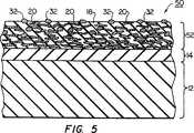
図5は、本発明による押しくぼませる粒子をもつエラスチック導電層を有する積層構成体の断面図である。
図6は、本発明による突き刺し粒子をもつエラスチック導電層を有する積層構成体の断面図である。
図7は、本発明によるエラスチック導電層を有する押しボタンスイッチの断面図である。
図8は、本発明によるエラスチック通電相互接続エレメントを有する相互接続デバイスの断面図である。
図9は、図8に示したエラスチック通電相互接続エレメントの一つの断面図である。
図10は、本発明によるエラスチック通電相互接続エレメントを成形する射出装置の断面図である。
図11は、本発明による導電性の押しくぼませる粒子をもつエラスチック通電相互接続エレメントの断面図である。
図12は、本発明による導電性の突き刺し粒子をもつエラスチック通電相互接続エレメントの断面図である。
発明の詳細な記述
図1を参照すると、エラスチックの基体12、エラスチックのプライマー層14及びエラスチックの導電層16を備える積層構成体10の断面が示されている。エラスチックの基体12は、例えば、シリコンラバー又はフルオロシリコンラバーのような多様のエラスチックマテリアルズの一つで作られる。エラスチックのプライマー層14も例えば、シリコンラバー又はフルオロシリコンラバーのような多様のエラスチックマテリアルズの一つで作られる。エラスチックの導電層16は、エラスチックマテリアルと相当量の導電性フレーク20との混合ものからなる。エラスチックマテリアル18は、例えば、シリコンラバー又はフルオロシリコンラバーのような多様のエラスチックマテリアルズの一つで作られる。導電性フレーク20は、例えば、銀、ニッケル又は炭素のような導電性マテリアルズ又は半導電性マリアルズの種々様々のタイプのもので作られる。また別に、導電性フレーク20は、導電性マテリアルズ、半導電性マテリアルズ又は、例えば銀、ニッケル又は炭素のような他の導電性又は半導電性マテリアルズで被覆されているか、或は、それらのマテリアルズが内部に散在している絶縁性マテリアルズで作られる。導電性フレークのサイズは、要求される導電性レベルに応じて変わる。
積層構成体10は、エラスチックの基板12を完全にキュアリングさせた状態で開始になるのが通例である熱融合(サーマルグラフト)プロセスにより作られる。ついで、エラスチックのプライマー層14をスプレイコーティング又は他の既知の手段によりエラスチックの基板12に被着する。積層構造体全体をサーマルサイクルに付し、これによって、エラスチックのプライマー層14を完全にキュアーさせ、エラスチックの基板12に接合させ、そして、導電層16を完全にキュアーさせ、エラスチックのプライマー層14に接合させる。このサーマルグラフトプロセスの間、エラスチックのプライマー層14のポリマー鎖がエラスチックの基板12のポリマー鎖にグラフトし、強力な接合を形成する。同様に、エラスチックの導電層16におけるポリマー鎖がエラスチックのプライマー層14におけるポリマー鎖にグラフトし、強力な接合を形成する。このサーマルグラフトプロセスによって、エラスチックの基板12の面をエッチングしたり、又は、その他の前処理の必要がなくなる。
エラスチックの基板12の厚さには、大まかには制限がない。エラスチックのプライマー層14とエラスチックの導電層16とを組み合わせたものの厚みは、0.5ミルから10ミルの間が代表的なものである。大まかに言えば、エラスチックの導電層16は、エラスチックのプライマー層14の2倍の厚みである。エラスチックマテリアルズすべてのデュロメーターレートは、ショアーAスケールで40から80の間のレンジにあるのが代表的なものである。上記した特性をすべて有するエラスチックの導電層16の抵抗は、プリント回路基板におけるSn/Pbトレースにエラスチック導電層16の面を押接することによって行われた測定の間、20〜30mohmの範囲にあることが示されている。
エラスチックの導電層16のエラスチックマテリアル18内に懸架されている導電性フレーク20は、エラスチックの導電層16が膨張又は圧縮されて変形するときでも、抵抗が低く、これは、導電性フレーク20の表面領域が、そのような変形が生じたとしても、隣接する導電性フレーク20の間で電気的に接触するに充分な大きさを有しているからである。例えば、エラスチックの導電層16が長さ方向に膨張している間、エラスチックの導電層16の長さは、長くなる一方、エラスチックの導電層16の厚さは、薄くなる。この厚さが薄くなることで、隣接する導電性フレーク20は、互いに密着し合い、これによって、隣接の導電性フレーク20の広い表面領域は,フィジカルに、そしてしたがって、電気的に、互いに接触する蓋然性が高くなる。長さが長くなることは、導電性フレーク20が横方向に動くことになり、これによって、隣接の導電性フレーク20の広い表面領域が互いに擦れたり、すれたりし、その結果、隣接の導電性フレーク20の間にフィジカルの、そしてしたがって、電気的の接触が保たれる。
上記の積層構成体10の有用な一つの特定の応用面は、電話器又は計算機のキイパッドであり、ここでは、キイパッドのキイを押すことで電気導通がなされなければならない。このようなキイパッドを例えばシリコンラバーやフルオロシリコンラバーのようなエラスチックのマテリアルで構成するとすると、エラスチックの導電層は、上記したプロセスによりエラスチックのマテリアルの面にグラフトすることができる。したがって、前記キイパッドのキイを相手となる導電デバイス、例えばプリント回路基板の導電性トレースのようなものに対し押せば、前記エラスチックの導電層と前記導電トレースとの間に電気が導通することになる。
図2を参照すると、内部にキイ104を形成したエラスチックのカバー102を備える電話機又は計算機のキイパッド100の断面が示されている。カバー102のカバー102の下側、各キイ104の下で、エラスチックのプライマー層106がエラスチックのカバー102に接合され、エラスチックの導電層108がエラスチックのプライマー層106に接合されている。
プリント回路基板110が全体のカバー102の下に位置し、導電トレース112がキイ104の下のプリント回路基板110に形成されている。かくして、例えば、人の指114からエラスチックのカバー102のキイ104の一つに力Fが加えられると、エラスチックの導電層108は、導電トレース112の対応する一つと電気的に接触することになる。
図3を参照すると、図1に記載した積層構成体10に類似しているが、エラスチックの導電層16の面に導電性の押しくぼませる粒子32をしっかりはめ込んである積層構成体30の断面が示してある。該導電性の押しくぼませる粒子32は、前記サーマルサイクル(熱処理)に先立ってエラスチックの導電層16の面に施されるものであり、その結果、該粒子32は、前記導電層が完全にキュアーすると、エラスチックの導電層16にしっかり保持される。導電性の押しくぼませる粒子32の押しくぼませるのインデントする形態によって、エラスチックの導電層16に接触すべき導電面に形成される絶縁性酸化物が押し退けられ、この結果、導電面とエラスチックの導電層16との間に改善された電気接続が形成される。前記導電性の押しくぼませる粒子32は、相手の導電面に存在する繊維及び粒子のような他の汚染物を押し退ける点に注目すべきである。
導電性の押しくぼませる粒子32は、例えば、銀、ニッケル又は炭素のような種々様々のタイプの導電性又は半導電性マテリアルズで作られる。また別に、導電性の押しくぼませる(インデンティング)粒子32は、導電性マテリアルズ、半導電性マテリアルズ、又は、例えば銀、ニッケル又は炭素のような他の導電性又は半導電性マテリアルズで被覆されているか、或は、それらのマテリアルズが内部に散在している絶縁性マテリアルズで作られる。導電性の押しくぼませる粒子32の代表的な平均粒子サイズは50μmである。
図4を参照すると、図1に記載した積層構成体10に類似しているが、エラスチックの導電層16の面に導電性の突き刺し(ピアシング)粒子42をしっかりはめ込んである積層構成体40の断面が示してある。導電性突き刺し粒子42は、前記サーマルサイクル(熱処理)に先立ってエラスチックの導電層16の面に施されるものであり、その結果、該粒子42は、前記導電層が完全にキュアーすると、エラスチックの導電層16にしっかり保持される。導電性の突き刺し粒子42の突き刺し作用によって、エラスチックの導電層16に接触すべき導電面に形成される絶縁性酸化物が突き刺されて該粒子が貫通し、この結果、導電面とエラスチックの導電層16との間に改善された電気接続が形成される。前記導電性の突き刺し粒子42は、相手の導電面に存在する繊維及び粒子のような他の汚染物を突き刺し貫通する点に注目すべきである。
導電性の押しくぼませる粒子32と同様に、導電性の突き刺し粒子42は、例えば、銀、ニッケル又は炭素のような種々様々のタイプの導電性又は半導電性マテリアルズで作られる。また別に、導電性の突き刺し粒子42は、導電性マテリアルズ、半導電性マテリアルズ、又は、例えば銀、ニッケル又は炭素のような他の導電性又は半導電性マテリアルズで被覆されているか、或は、それらのマテリアルズが内部に散在している絶縁性マテリアルズで作られる。導電性の突き刺し粒子32の代表的な平均粒子サイズは40μmである。
図5を参照すると、図1に記載した積層構成体10に類似しているが、エラスチックのマテリアル18、導電性フレーク20及び導電性の押しくぼませる粒子32を備えるエラスチックの導電層52をもつ積層構成体50の断面が示されている。この積層構成体50を作るには、導電性の押しくぼませる粒子32をエラスチックマテリアル18と導電性フレーク20と共にエラスチックのプライマー層14にデポジットする。エラスチックの導電層52における導電性の押しくぼませる粒子32の分布域は、エラスチックの導電層52の面に近接して示されており、これは、エラスチックの導電層52を施す間、導電性の押しくぼませる粒子32が導電性フレーク20よりもエラスチックのプライマー層14から離れやすいからである。当然なことであるが、導電性の押しくぼませる粒子32にとって、このような位置は、それらの機能(例えば、相手の導電面の酸化物を押し除く)の面で好ましい。エラスチックの導電層52における導電性の押しくぼませる粒子32の量は、該粒子の適正な機能を確実にさせるために、代表的には、僅か5重量%ノミナルを必要とする。
図6を参照すると、図1に記載した積層構成体10に類似しているが、エラスチックのマテリアル18、導電性フレーク20及び導電性の突き刺し粒子42を備えるエラスチックの導電層62をもつ積層構成体60の断面が示されている。この積層構成体60を作るには、導電性の突き刺し粒子42をエラスチックマテリアル18と導電性フレーク20と共にエラスチックのプライマー層14にデポジットする。エラスチックの導電層62における導電性の突き刺し粒子42の分布域は、エラスチックの導電層62の面に近接して示されており、これは、エラスチックの導電層62を施す間、導電性の突き刺し粒子42が導電性フレーク20よりもエラスチックのプライマー層14から離れやすいからである。当然なことであるが、導電性の突き刺し粒子42にとって、このような位置は、それらの機能(例えば、相手の導電面の酸化物を突き刺し貫通する)の面で好ましい。エラスチックの導電層62における導電性の突き刺し粒子42の量は、該粒子の適正な機能を確実にさせるために、代表的には、僅か5重量%ノミナルを必要とする。
このポイントで、注目すべき点は、上記した積層構成体10,30,40,50及び60のすべてにおけるエラスチックの基体12を例えば、熱可塑性プラスチックス・ポリイミド(商標captonとして知られている)又はポリアミド(商標nylonとして知られている)のような単にフレキシブルのものに代替できる点である。エラスチックのプライマー層14は、上記した態様で、そのようなフレキシブルな基体に対しグラフト接合され、それと共にエラスチックの導電層16をエラスチックのプライマー層14にグラフトする。
フレキシブルの基体である点を除いて、上記した積層構成体10,30,40,50及び60の一つに類似した積層構成体の有用な応用面は、電気導通を押しボタンスイッチを押すことで行う押しボタンスイッチである。そのようなスイッチのボタンを例えばポリイミド又はポリアミド・サーマルプラスチックのようなフレキシブルのマテリアルで作ると、上記したプロセスによりエラスチックの導電層をエラスチックのマテリアルの面にグラフトできる。かくて、そのようなスイッチのボタンを金属接点のような相手の導電デバイスに対し押すと、エラスチックの導電層と金属接点との間に電気が通電することになる。
図7を参照すると、リコイルスプリング204内蔵のハウジング202とボタンアクチュエーター206とを備える押しボタンスイッチ200の断面が示されている。ハウジング202は、その内部へアクセスする金属接点208を設けている。
ボタンアクチェーター206は、例えば、ポリイミド又はポリアミドのようなフレキシブルのサーマルプラスチックマテリアルで作られている。エラスチックのプライマー層210は、ボタンアクチュエーター206の底部接触面に接合され、エラスチックの導電層212は、エラスチックのプライマー層210に接合されている。ボタンアクチュエーター206へ力Fが加えられると、エラスチックの導電層212は、金属接点208と電気接触し、これによってスイッチ200が閉成される。
このポイントで注目すべき点は、上記した積層構成体10,30,40,50,60のいずれも図2の電話機又は計算機のキイパッド100又は図7の押しボタンスイッチ200に利用でき、又は、エラスチックの導電層の使用が有用になる種々の他のデバイスに利用できる点である。
また注目すべき点は、上記した積層構成体10,30,40,50,60のすべてに用いられているエラスチックの導電層16,52,62,108,212が電界又は磁界とのシールド又は接地目的その他の導電プレーンの付与に有用な点である。さらに詳しくは、上記エラスチックの導電層15,52,62,108,212における導電性フレーク20の密度及びグルーピングは、極めて効果があるシールド層又は接地層になるものである。上記したエラスチックの導電層15,52,62,108,212は、また、プリント回路基板の導電トレースに対し、エラスチックの導電層15,52,62,108,212を押し付けることにより、前記導電トレースとの電気接続形成に使用される。
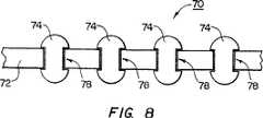
図8を参照すると、開口78を配列形成した絶縁基体72を備える相互接続デバイス70の断面が示されている。エラスチックの導電性相互接続エレメント74が各開口78内に配置されている。このような相互接続デバイス70は、例えば、リードレス集積回路パッケージの電気接点と、プリント回路基板の電気接点とを電気的に接続するために用いられるものである。これら電気接点は、ボール又はランドグリッド配列バラエティを有している。
図9を参照すると、エラスチックの導電性相互接続エレメント74の断面が示されている。エラスチックの導電性相互接続エレメント74は、エラスチックマテリアル18、導電性フレーク20及び導電性粉末顆粒76の混合物からなる。導電性粉末顆粒76は、例えば、銀、ニッケル又は炭素のような導電性又は半導電性マテリアルズから作られる。導電性粉末顆粒76のサイズは、要求される導電性のレベルに応じて変わる。
導電性粉末顆粒76により導電性フレーク20の間に導電ブリッジが形成され、これによって、エラスチックの相互接続エレメント74の電気導通性が高まる。そのような電気導通性を高めるために、エラスチックマテリアル18と導電性フレーク20との混合物に加えるべき導電性粉末顆粒76の量は、要求される導通性のレベルに応じて変わる。
図10を参照すると、絶縁基体72の開口78内にエラスチックの導電性相互接続エレメント74を形成するための射出装置80の断面が示されている。該装置80は、射出経路84を内部に形成した上型82と下型86を備えている。エラスチックマテリアル18、導電性フレーク20及び導電性粉末顆粒76の混合物は、経路84を経て流れ、上型82と下型86との間の空隙及び絶縁基体72の開口78に充填される。前記混合物は、初めには加熱されているが、その後冷却されてキュアーする。冷却により前記混合物は、膨張し、この結果、エラスチックの導電性相互接続エレメント74は、開口78内に確実に位置する注目すべき点は、前記相互接続エレメントの領域における上型82と下型86の形状を相互接続エレメントの特定の応用面(例えば、相互接続ランドグリッド配列接点又は相互接続ボールグリッド配列接点)に応じて変えることができる点である。
図11を参照すると、図9に示したエラスチックの導電性相互接続エレメント74に類似しているが、エラスチックのマテリアル18、導電性フレーク20及び導電性の粉末顆粒76の混合物に導電性の押しくぼませる粒子32をもつエラスチックの導電性相互接続エレメント90の断面が示されている。図5に記載したエラスチックの導電層52と同様に、導電性相互接続エレメント90における導電性の押しくぼませる粒子32の量は、それらの適正な機能を確保するために、代表的には、僅か5重量%ノミナルが必要である。注目すべき点は、導電性の押しくぼませる粒子32を、エラスチックの導電性相互接続エレメントの表面のみに対し、該エレメントが成形され、しかもそれがキュアーする前に、添加することができる点である。
図12を参照すると、図9に示したエラスチックの導電性相互接続エレメント74に類似しているが、エラスチックのマテリアル18、導電性フレーク20及び導電性の粉末顆粒76の混合物に導電性の突き刺し粒子42をもつエラスチックの導電性相互接続エレメント110の断面が示されている。図6に記載したエラスチックの導電層62と同様に、導電性相互接続エレメント90における導電性の突き刺し粒子42の量は、それらの適正な機能を確保するために、代表的には、僅か5重量%ノミナルが必要である。注目すべき点は、導電性の突き刺し粒子42を、エラスチックの導電性相互接続エレメントの表面のみに対し、該エレメントが成形され、しかもそれがキュアーする前に、添加することができる点である。
本発明は、ここに記載の特定の実施例による範囲に限定されるものではない。実際に、ここに記載のものに加えて、本発明の種々のモディフィケーションは、前記の記述と添付の図面から当業者にとり明らかなものである。かくてそのようなモディフィケーションは、添付の請求の範囲の範囲に入るべきものである。Cross-reference of related applications
This patent application is a continuation-in-part of U.S. patent application Ser. No. 08 / 294,370, filed Aug. 23, 1994 and U.S. patent application Ser. No. 08 / 348,574, filed Dec. 2, 1994.
Field of Invention
The present invention relates to a conductive device, and more particularly to a conductive elastomer and a method for producing the same.
Background of the Invention
Advances in integrated circuits have reduced the package size of integrated circuits, while increasing the number of electrical leads that make electrical interconnections between the integrated circuit and the circuit board on which the circuit is located. As the number of electrical leads for each integrated circuit increased, the size of the electrical leads became smaller and the spacing became closer, thereby increasing the difficulty of mounting the integrated circuit on the circuit board.
One way to overcome this problem is to replace the electrical leads placed around the periphery of the integrated circuit package with electrical contacts located on the bottom of the integrated circuit package to form a leadless integrated circuit package. It is to be. These electrical contacts are generally small protrusions or “balls” in shape and are spaced apart by a grid array turn. These integrated circuit packages with bottom electrical contacts are placed in a leadless integrated circuit socket or in a mounting device that holds the integrated circuit package. The mounting device has a plurality of abutting electrical contacts spaced in a grid array pattern, which are aligned with the electrical contacts of the integrated circuit, an integrated circuit package, and a circuit board on which the mounting device is located. Conduct electricity between.
One problem that arises in leadless integrated circuit packages is that the electrical contacts of the leadless integrated circuit package and the electrical contacts that are mated to the mounting device are oxidized, thereby increasing the contact resistance, and thus the electrical contacts of the integrated circuit package. The electrical continuity between the electrical contact between the device and the mounting device is reduced. The insertion force when mounting a leadless integrated circuit package typically removes some of this oxide, thereby improving electrical contact. However, leadless integrated circuit packages are generally not inserted into mounting devices to remove oxides of electrical contacts, and leadless integrated circuit packages are soldered directly to mounting devices. Since this is not done, oxide accumulates in the electrical contacts, resulting in poor electrical contact.
Another problem that arises in leadless integrated circuit packages is that the electrical contacts of the mounting device are in electrical communication with the electrical contacts that are soldered directly to the circuit board. For this reason, if it is necessary to replace or remove the mounting device, the soldered portion of the mounting device must be removed. As is generally known in the industrial field, repeated soldering and repeated removal of solder to locations that require replacement usually impairs the quality of the circuit board. Thus, an electrical connection scheme without soldering is desirable.
When manufacturing electronic or electrical devices and circuits, the conductive paths and contact areas are typically provided by chemical etching and photolithographic techniques and plating techniques, such as circuit boards, when manufacturing printed circuit boards. Are provided with electrical contacts or electrical contact areas. Such manufacturing techniques are well known and widely used. However, these technologies require a number of process steps and specialized manufacturing equipment, which affects the cost and complexity of the manufacturing process and the resulting product cost and complexity. Thus, a simpler manufacturing technique is desired.
Summary of the Invention
The present invention contemplates several types of conductive elastomers and methods for making them. In one embodiment, the present invention is implemented as a laminated composition, the composition comprising a substrate comprising an electrically non-conductive elastic material having an outer surface; grafted to the outer surface of the substrate A first layer formed from an electrically non-conductive elastic material; and a second layer grafted to the first layer and formed from an electrically non-conductive elastic material; And a second layer having a substantial amount of conductive flakes scattered therein. The second layer is interspersed in the electrically non-conductive material, and the scattered aspect is rounded in such a way that some conductive particles are present along the outer surface of the second layer. Or it is further formed with jagged conductive particles. Alternatively, a considerable amount of rounded or jagged conductive material may be embedded in the second layer.
In another embodiment, the present invention provides an elastic energization formed of an electrically non-conductive material having an elongated shape and a substantial amount of conductive flakes and a substantial amount of conductive powder particles interspersed therein. Implemented as an interconnect element. This elastic energizing interconnect element has a substantial amount of rounded or jagged conductive particles scattered within an electrically non-conductive elastic material, with some of the conductive particles being in the elastic It can be formed to exist along the outer surface of the energized interconnection element.
In yet another embodiment, the present invention provides an electrically non-conductive substrate having opposing faces and a plurality of holes extending between the opposing faces; and the plurality of holes Is realized as an electrical interconnect comprising an electrically non-conductive substrate comprising a corresponding plurality of elastic conductive interconnect elements located inside the substrate, wherein each elastic conductive interconnect element comprises: An electrically non-conductive elastic material extending between respective opposing surfaces of the substrate and each elastic conductive interconnect element interspersed with a substantial amount of conductive flakes and a substantial amount of conductive powder granules. It is made with.
The present invention includes a method of manufacturing the above-described structure, which is unique per se by a novel manufacturing process.
Accordingly, it is a primary object of the present invention to provide electrically conductive elastomers and methods for making them.
The above main objects and other objects, features and advantages of the present invention will become readily apparent from the following detailed description which should be read in conjunction with the accompanying drawings.
Brief description of the drawings
To facilitate a more complete understanding of the present invention, reference is now made to the accompanying drawings. These drawings should not be construed as limiting the invention, but are exemplary only.
FIG. 1 is a cross-sectional view of a stacked structure having an elastic conductive layer according to the present invention.
FIG. 2 is a cross-sectional view of a telephone or calculator keypad having an elastic conductive layer according to the present invention.
FIG. 3 is a cross-sectional view of a laminate structure having an elastic conductive layer according to the present invention and particles to be depressed.
FIG. 4 is a cross-sectional view of a laminated structure having an elastic conductive layer according to the present invention and piercing particles.
FIG. 5 is a cross-sectional view of a laminate structure having an elastic conductive layer with indented particles according to the present invention.
FIG. 6 is a cross-sectional view of a laminated structure having an elastic conductive layer with piercing particles according to the present invention.
FIG. 7 is a cross-sectional view of a pushbutton switch having an elastic conductive layer according to the present invention.
FIG. 8 is a cross-sectional view of an interconnect device having an elastic energized interconnect element according to the present invention.
FIG. 9 is a cross-sectional view of one of the elastic energization interconnection elements shown in FIG.
FIG. 10 is a cross-sectional view of an injection apparatus for molding an elastic energizing interconnect element according to the present invention.
FIG. 11 is a cross-sectional view of an elastic energizing interconnect element with conductive indenting particles according to the present invention.
FIG. 12 is a cross-sectional view of an elastic energized interconnect element with conductive piercing particles according to the present invention.
Detailed description of the invention
Referring to FIG. 1, a cross section of a laminate structure 10 comprising an
The laminated structure 10 is made by a thermal fusion process, which typically begins with the
The thickness of the
The
One useful particular application of the above laminated structure 10 is a telephone or calculator keypad, where electrical conduction must be achieved by pressing the keypad key. When such a keypad is made of an elastic material such as silicon rubber or fluorosilicone rubber, the elastic conductive layer can be grafted onto the surface of the elastic material by the above-described process. Therefore, if the key of the keypad is pressed against an opposing conductive device, such as a printed circuit board conductive trace, electricity will be conducted between the elastic conductive layer and the conductive trace. .
Referring to FIG. 2, there is shown a cross-section of a telephone or
A printed
Referring to FIG. 3, a cross-section of a
The
Referring to FIG. 4, a cross-section of a laminate structure 40 similar to the laminate structure 10 described in FIG. 1, but with conductive piercing
Similar to the conductive indenting
Referring to FIG. 5, a laminate similar to the laminate structure 10 described in FIG. 1, but with an elastic conductive layer 52 comprising
Referring to FIG. 6, a laminated structure similar to the laminated structure 10 described in FIG. 1, but having an elastic conductive layer 62 comprising an
At this point, it should be noted that the
A useful application aspect of a laminated structure similar to one of the
Referring to FIG. 7, a cross section of a
The
In this respect, it should be noted that any of the
Also, it should be noted that the elastic
Referring to FIG. 8, a cross section of an
Referring to FIG. 9, a cross section of an elastic
The
Referring to FIG. 10, a cross-section of an
Referring to FIG. 11, similar to the elastic
Referring to FIG. 12, conductive piercing particles similar to the elastic
The present invention is not limited to the scope of the specific embodiments described herein. Indeed, various modifications of the invention, in addition to those described herein, will be apparent to those skilled in the art from the foregoing description and accompanying drawings. Thus, such modifications are intended to fall within the scope of the appended claims.
Claims (54)
Translated fromJapanese外表面を有し、電気不導通性マテリアルから形成されている基体;
前記基体の前記外表面の少なくとも一部に接合され、外表面を有していて、電気不導通性マテリアルから形成されている第1の層;及び
前記第1の層の前記外表面の少なくとも一部に接合され、外表面を有していて、導電性フレークが内部に散在している電気不導通性エラスチックマテリアルから形成されている第2の層であって、
ここで、前記第2の層の前記外表面が押圧されると、該押圧に係る応力に対して垂直方向に電気導通性となる前記第2の層。Laminated construction comprising:
A substrate having an outer surface and formed from an electrically non-conductive material;
A first layer bonded to at least a portion of the outer surface of the substrateand having an outer surface and formed of an electrically non-conductive material; and at least one of the outer surfaces ofthe first layer; A second layer formed from an electrically non-conductive elastic material joined to a portion, having an outer surface, and having conductive flakes interspersed therein,
Here, when the outer surface of the second layer is pressed, the second layer becomes electrically conductive in a direction perpendicular to the stress applied to the pressing.
該長手方向の横方向から応力がかかるとその垂直方向である長手方向に電気導通性となる前記エラスチックの導電性接続エレメント。An elastic conductive interconnect element, wherein the elastic conductive interconnect element has an elongated shape and is electrically connected in the longitudinal direction, and the elastic conductive interconnect element comprises: Formed of electrically non-conductive elastic material with conductive flakes and conductive powder granules scattered inside,
The elastic conductive connecting element which becomes electrically conductive in a longitudinal direction which is a vertical direction when stress is applied from a lateral direction of the longitudinal direction.
外表面を有し、電気不導通性エラスチックマテリアルで形成されている基体を調製し;
前記基体の前記外表面の少なくとも一部に第1の層を施す工程で、前記第1の層は、外表面を有し、電気不導通性のエラスチックのマテリアルで形成されており;
前記第1の層の前記外表面の少なくとも一部に第2の層を施す工程で、前記第2の層は、外表面を有し、導電性フレークが内部に散在している電気不導通性エラスチックマテリアルで前記第2の層が形成されており;
前記基体、前記第1の層及び前記第2の層をサーマルプロセスで処理し、前記第1の層を前記基体に接合し、前記第2の層を前記第1の層に接合する工程。A method for producing an elastic laminate structure according to claim 1 having a conductive surface, the method comprising the following steps:
Preparing a substrate having an outer surface and formed of an electrically non-conductive elastic material;
Applying a first layer to at least a portion of the outer surface of the substrate, wherein the first layer has anouter surface and is formed of an electrically non-conductive elastic material;
In the step of applying a second layer to at least a portion ofsaid outer surface of said first layer, said second layer has an outer surface, electrical non conductivity of conductive flakes interspersed therein The second layer is formed of an elastic material;
Treating the substrate, the first layer, and the second layer by a thermal process, bonding the first layer to the substrate, and bonding the second layer to the first layer;
それぞれ対向する面をもつ基体で、前記それぞれ対向する面の間を貫通形成された複数の開口を有して、電気不導通性マテリアルで形成されている基体;及び
前記複数の開口内に位置する対応する複数のエラスチックの相互接続エレメントで、各前記エラスチックの導電性相互接続エレメントは、前記基体の前記それぞれ対向する面の間に延びており、各前記エラスチックの導電性相互接続エレメントは、導電性フレークと導電性粉末顆粒とが内部に散在する電気不導通性エラスチックマテリアルで形成されており、
ここで、前記対向する面間の方向に応力がかかると、該方向に対して垂直方向に電気導通性となる前記エレメント。Electrical interconnection device comprising:
A base body having opposing faces each having a plurality of openings penetrating between the opposing faces and formed of an electrically non-conductive material; and located within the plurality of openings A plurality of corresponding elastic interconnection elements, each elastic conductive interconnection element extending between the respective opposing surfaces of the substrate, and each elastic conductive interconnection element is electrically conductive; It is made of electrically non-conductive elastic material with flakes and conductive powder granules scattered inside,
Here, when stress is applied in a direction between the opposing surfaces, the element becomes electrically conductive in a direction perpendicular to the direction.
Applications Claiming Priority (3)
| Application Number | Priority Date | Filing Date | Title |
|---|---|---|---|
| US08/736,830US5949029A (en) | 1994-08-23 | 1996-10-28 | Conductive elastomers and methods for fabricating the same |
| US08/736,830 | 1996-10-28 | ||
| PCT/US1996/019243WO1998018615A1 (en) | 1996-10-28 | 1996-12-03 | Conductive elastomers and methods for fabricating the same |
Publications (2)
| Publication Number | Publication Date |
|---|---|
| JP2002514342A JP2002514342A (en) | 2002-05-14 |
| JP4082735B2true JP4082735B2 (en) | 2008-04-30 |
Family
ID=24961464
Family Applications (1)
| Application Number | Title | Priority Date | Filing Date |
|---|---|---|---|
| JP52041498AExpired - Fee RelatedJP4082735B2 (en) | 1996-10-28 | 1996-12-03 | Conductive elastomers and methods for making them |
Country Status (7)
| Country | Link |
|---|---|
| US (1) | US5949029A (en) |
| EP (1) | EP0912335B1 (en) |
| JP (1) | JP4082735B2 (en) |
| CN (1) | CN1304196C (en) |
| CA (1) | CA2241530C (en) |
| DE (1) | DE69627389T2 (en) |
| WO (1) | WO1998018615A1 (en) |
Cited By (1)
| Publication number | Priority date | Publication date | Assignee | Title |
|---|---|---|---|---|
| JPWO2015025660A1 (en)* | 2013-08-19 | 2017-03-02 | ポリマテック・ジャパン株式会社 | connector |
Families Citing this family (38)
| Publication number | Priority date | Publication date | Assignee | Title |
|---|---|---|---|---|
| US6271482B1 (en)* | 1994-08-23 | 2001-08-07 | Thomas & Betts International, Inc. | Conductive elastomer interconnect |
| AU2039801A (en) | 1999-10-22 | 2001-05-08 | Government of the United States of America as represented by the Administrator of the National Aeronautics and Space Administration (NASA), The | Electrostrictive graft elastomers |
| US6264476B1 (en) | 1999-12-09 | 2001-07-24 | High Connection Density, Inc. | Wire segment based interposer for high frequency electrical connection |
| TW508440B (en)* | 1999-12-27 | 2002-11-01 | Hoya Co Ltd | Probe structure and manufacturing method thereof |
| WO2002035289A2 (en)* | 2000-10-24 | 2002-05-02 | Nanopierce Technologies Inc. | Method and materials for printing particle-enhanced electrical contacts |
| US7083436B2 (en) | 2001-03-06 | 2006-08-01 | International Business Machines Corporation | Particle distribution interposer and method of manufacture thereof |
| US7222243B2 (en) | 2001-04-26 | 2007-05-22 | Tyco Electronics Corporation | Power delivery system for a microprocessor |
| US6815039B2 (en)* | 2002-02-21 | 2004-11-09 | Bei Technologies, Inc. | Resistance element for potentiometric devices, and method of manufacture |
| US7014479B2 (en)* | 2003-03-24 | 2006-03-21 | Che-Yu Li | Electrical contact and connector and method of manufacture |
| US7040902B2 (en)* | 2003-03-24 | 2006-05-09 | Che-Yu Li & Company, Llc | Electrical contact |
| US7029288B2 (en)* | 2003-03-24 | 2006-04-18 | Che-Yu Li | Electrical contact and connector and method of manufacture |
| US20060091538A1 (en)* | 2004-11-04 | 2006-05-04 | Kabadi Ashok N | Low profile and tight pad-pitch land-grid-array (LGA) socket |
| US8071174B2 (en) | 2009-04-03 | 2011-12-06 | John Mezzalingua Associates, Inc. | Conductive elastomer and method of applying a conductive coating to elastomeric substrate |
| US8157589B2 (en) | 2004-11-24 | 2012-04-17 | John Mezzalingua Associates, Inc. | Connector having a conductively coated member and method of use thereof |
| EP1839372B1 (en)* | 2004-12-21 | 2011-07-13 | Eles Semiconductor Equipment S.P.A. | Production processes for a system for contacting electronic devices |
| DE102006033711B4 (en) | 2006-07-20 | 2012-06-14 | Epcos Ag | Method for producing a resistor arrangement |
| US7585173B2 (en)* | 2007-03-30 | 2009-09-08 | Tyco Electronics Corporation | Elastomeric electrical contact |
| US8113875B2 (en) | 2008-09-30 | 2012-02-14 | Belden Inc. | Cable connector |
| US7824216B2 (en)* | 2009-04-02 | 2010-11-02 | John Mezzalingua Associates, Inc. | Coaxial cable continuity connector |
| US8816205B2 (en)* | 2009-04-03 | 2014-08-26 | Ppc Broadband, Inc. | Conductive elastomer and method of applying a conductive coating to a cable |
| US8113879B1 (en) | 2010-07-27 | 2012-02-14 | John Mezzalingua Associates, Inc. | One-piece compression connector body for coaxial cable connector |
| US8157588B1 (en) | 2011-02-08 | 2012-04-17 | Belden Inc. | Cable connector with biasing element |
| US8465322B2 (en) | 2011-03-25 | 2013-06-18 | Ppc Broadband, Inc. | Coaxial cable connector |
| US8342879B2 (en) | 2011-03-25 | 2013-01-01 | John Mezzalingua Associates, Inc. | Coaxial cable connector |
| DE102012202225B4 (en)* | 2012-02-14 | 2015-10-22 | Te Connectivity Germany Gmbh | Plug housing with seal |
| US9459285B2 (en)* | 2013-07-10 | 2016-10-04 | Globalfoundries Inc. | Test probe coated with conductive elastomer for testing of backdrilled plated through holes in printed circuit board assembly |
| DE102014211239A1 (en)* | 2014-06-12 | 2015-12-17 | Benecke-Kaliko Ag | Foil with integrated sensors |
| US10104772B2 (en)* | 2014-08-19 | 2018-10-16 | International Business Machines Incorporated | Metallized particle interconnect with solder components |
| WO2016121662A1 (en)* | 2015-01-27 | 2016-08-04 | 日東電工株式会社 | Transparent electroconductive film |
| JP6580432B2 (en)* | 2015-03-16 | 2019-09-25 | 日東電工株式会社 | Transparent conductive film |
| JP6580431B2 (en)* | 2015-01-27 | 2019-09-25 | 日東電工株式会社 | Transparent conductive film |
| JP6804931B2 (en)* | 2016-02-22 | 2020-12-23 | オリンパス株式会社 | Anti-adhesion membrane for medical devices and medical devices |
| CN106340406B (en)* | 2016-08-30 | 2020-09-22 | 南通万德科技有限公司 | Composite material and preparation method thereof |
| JP6918518B2 (en)* | 2017-02-27 | 2021-08-11 | デクセリアルズ株式会社 | Electrical property inspection jig |
| US11128072B1 (en) | 2020-07-22 | 2021-09-21 | TE Connectivity Services Gmbh | Electrical connector assembly having variable height contacts |
| US11509080B2 (en) | 2020-07-22 | 2022-11-22 | Te Connectivity Solutions Gmbh | Electrical connector assembly having hybrid conductive polymer contacts |
| US11509084B2 (en) | 2020-07-24 | 2022-11-22 | Te Connectivity Solutions Gmbh | Electrical connector assembly having hybrid conductive polymer contacts |
| US11894629B2 (en) | 2021-03-09 | 2024-02-06 | Tyco Electronics Japan G.K. | Electrical interconnect with conductive polymer contacts having tips with different shapes and sizes |
Family Cites Families (65)
| Publication number | Priority date | Publication date | Assignee | Title |
|---|---|---|---|---|
| US3100933A (en)* | 1956-10-15 | 1963-08-20 | Gen Motors Corp | Method of cold welding aluminum |
| US3203083A (en)* | 1961-02-08 | 1965-08-31 | Texas Instruments Inc | Method of manufacturing a hermetically sealed semiconductor capsule |
| US3482726A (en)* | 1967-02-13 | 1969-12-09 | Arthur Henry Schroeder Jr | Pressure weld seal for a composite glass body and method of forming said seal |
| GB1198257A (en)* | 1967-04-29 | 1970-07-08 | Int Computers Ltd | Improvements in Methods of Bonding Electrical Conductors |
| US3698931A (en)* | 1969-06-18 | 1972-10-17 | Polymer Research Corp Of Ameri | Method of grafting polymerizable monomers onto substrates |
| US3700427A (en)* | 1969-07-11 | 1972-10-24 | Gen Electric | Powder for diffusion bonding of superalloy members |
| US3632319A (en)* | 1969-07-11 | 1972-01-04 | Gen Electric | Diffusion bonding of superalloy members |
| US3929800A (en)* | 1969-12-29 | 1975-12-30 | Polymer Research Corp Of Ameri | Polymer grafting onto hydrocarbon liquids |
| US3880580A (en)* | 1971-01-11 | 1975-04-29 | Polymer Research Corp Of Ameri | Method of activating polymeric materials |
| US3940377A (en)* | 1971-01-11 | 1976-02-24 | Polymer Research Corporation Of America | Method of activating polymers |
| US3818415A (en)* | 1973-02-16 | 1974-06-18 | Amp Inc | Electrical connections to conductors having thin film insulation |
| US3921885A (en)* | 1973-06-28 | 1975-11-25 | Rca Corp | Method of bonding two bodies together |
| US3971610A (en)* | 1974-05-10 | 1976-07-27 | Technical Wire Products, Inc. | Conductive elastomeric contacts and connectors |
| US4106955A (en)* | 1975-02-05 | 1978-08-15 | Gulf & Western Manufacturing Company | Coating steel surfaces |
| US4105811A (en)* | 1975-02-07 | 1978-08-08 | Polygulf Associates | Method of protectively coating metallic aluminum containing substrate |
| JPS5357481A (en)* | 1976-11-04 | 1978-05-24 | Canon Inc | Connecting process |
| JPS5826381B2 (en)* | 1979-04-28 | 1983-06-02 | 信越ポリマ−株式会社 | Electromagnetic shield gasket and its manufacturing method |
| US4563725A (en)* | 1983-01-06 | 1986-01-07 | Welwyn Electronics Limited | Electrical assembly |
| US4731282A (en)* | 1983-10-14 | 1988-03-15 | Hitachi Chemical Co., Ltd. | Anisotropic-electroconductive adhesive film |
| DE3339751A1 (en)* | 1983-11-03 | 1985-05-15 | BBC Aktiengesellschaft Brown, Boveri & Cie., Baden, Aargau | JOINT PROCESS |
| US4698275A (en)* | 1983-11-04 | 1987-10-06 | Augat Inc. | Wire mat mateable with a circuit board |
| US4688150A (en)* | 1984-06-15 | 1987-08-18 | Texas Instruments Incorporated | High pin count chip carrier package |
| FR2572856B1 (en)* | 1984-11-06 | 1988-01-08 | Socapex | LOW-STEP MINIATURE CONNECTING ELEMENT AND METHOD FOR MANUFACTURING SUCH A CONNECTING ELEMENT |
| US4593961A (en)* | 1984-12-20 | 1986-06-10 | Amp Incorporated | Electrical compression connector |
| US4894706A (en)* | 1985-02-14 | 1990-01-16 | Nippon Telegraph And Telephone Corporation | Three-dimensional packaging of semiconductor device chips |
| US4963425A (en)* | 1985-03-05 | 1990-10-16 | Unisys Corporation | Printed wiring board substrate for surface mounted components |
| US4659872A (en)* | 1985-04-30 | 1987-04-21 | Amp Incorporated | Flexible flat multiconductor cable |
| US5175409A (en)* | 1985-06-20 | 1992-12-29 | Metcal, Inc. | Self-soldering flexible circuit connector |
| US4754546A (en)* | 1985-07-22 | 1988-07-05 | Digital Equipment Corporation | Electrical connector for surface mounting and method of making thereof |
| US4778950A (en)* | 1985-07-22 | 1988-10-18 | Digital Equipment Corporation | Anisotropic elastomeric interconnecting system |
| JPS62201242A (en)* | 1986-02-28 | 1987-09-04 | 新興化学工業株式会社 | Silicone-resin laminated board and manufacture thereof |
| KR900008647B1 (en)* | 1986-03-20 | 1990-11-26 | 후지쓰 가부시끼가이샤 | A method for manufacturing three demensional i.c. |
| US4954875A (en)* | 1986-07-17 | 1990-09-04 | Laser Dynamics, Inc. | Semiconductor wafer array with electrically conductive compliant material |
| US4737112A (en)* | 1986-09-05 | 1988-04-12 | American Telephone And Telegraph Company, At&T Bell Laboratories | Anisotropically conductive composite medium |
| US4797508A (en)* | 1986-09-19 | 1989-01-10 | Firan Corporation | Method for producing circuit boards with deposited metal patterns and circuit boards produced thereby |
| US5065282A (en)* | 1986-10-17 | 1991-11-12 | Polonio John D | Interconnection mechanisms for electronic components |
| AU8118587A (en)* | 1986-11-17 | 1988-05-19 | Exicom Australia Pty Limited | Improved membrane keyboard |
| US4758927A (en)* | 1987-01-21 | 1988-07-19 | Tektronix, Inc. | Method of mounting a substrate structure to a circuit board |
| JPS63249393A (en)* | 1987-04-03 | 1988-10-17 | シャープ株式会社 | How to connect electronic components |
| US4804132A (en)* | 1987-08-28 | 1989-02-14 | Difrancesco Louis | Method for cold bonding |
| US4847146A (en)* | 1988-03-21 | 1989-07-11 | Hughes Aircraft Company | Process for fabricating compliant layer board with selectively isolated solder pads |
| US4847136A (en)* | 1988-03-21 | 1989-07-11 | Hughes Aircraft Company | Thermal expansion mismatch forgivable printed wiring board for ceramic leadless chip carrier |
| US5670251A (en)* | 1990-02-14 | 1997-09-23 | Particle Interconnect Corporation | Patternable particle filled adhesive matrix for forming patterned structures between joined surfaces |
| US5083697A (en)* | 1990-02-14 | 1992-01-28 | Difrancesco Louis | Particle-enhanced joining of metal surfaces |
| US5118299A (en)* | 1990-05-07 | 1992-06-02 | International Business Machines Corporation | Cone electrical contact |
| US5173766A (en)* | 1990-06-25 | 1992-12-22 | Lsi Logic Corporation | Semiconductor device package and method of making such a package |
| US5148266A (en)* | 1990-09-24 | 1992-09-15 | Ist Associates, Inc. | Semiconductor chip assemblies having interposer and flexible lead |
| US5092774A (en)* | 1991-01-09 | 1992-03-03 | National Semiconductor Corporation | Mechanically compliant high frequency electrical connector |
| US5106308A (en)* | 1991-03-04 | 1992-04-21 | Allied-Signal Inc. | Planar contact grid array connector |
| US5536568A (en)* | 1991-03-12 | 1996-07-16 | Inabagomu Co., Ltd. | Variable-resistance conductive elastomer |
| JPH04329277A (en)* | 1991-04-30 | 1992-11-18 | I T T Canon:Kk | Printed board connecting device |
| US5237203A (en)* | 1991-05-03 | 1993-08-17 | Trw Inc. | Multilayer overlay interconnect for high-density packaging of circuit elements |
| US5220726A (en)* | 1991-06-26 | 1993-06-22 | Xerox Corporation | Method for manufacturing an electrically connectable module |
| US5175491A (en)* | 1991-09-18 | 1992-12-29 | Sgs-Thomson Microelectronics, Inc. | Integrated circuit testing fixture |
| US5270571A (en)* | 1991-10-30 | 1993-12-14 | Amdahl Corporation | Three-dimensional package for semiconductor devices |
| DE9201284U1 (en)* | 1991-11-21 | 1992-03-19 | Silitek Corp., Taipeh/T'ai-Pei | Key switch |
| US5281852A (en)* | 1991-12-10 | 1994-01-25 | Normington Peter J C | Semiconductor device including stacked die |
| US5371327A (en)* | 1992-02-19 | 1994-12-06 | Shin-Etsu Polymer Co., Ltd. | Heat-sealable connector sheet |
| JP2534003B2 (en)* | 1992-03-17 | 1996-09-11 | 信越化学工業株式会社 | Laminated rubber molding |
| EP0562571B1 (en)* | 1992-03-25 | 1996-07-17 | Molex Incorporated | Printed circuit module |
| US5273440A (en)* | 1992-05-19 | 1993-12-28 | Elco Corporation | Pad array socket |
| US5267867A (en)* | 1992-09-11 | 1993-12-07 | Digital Equipment Corporation | Package for multiple removable integrated circuits |
| CN2143600Y (en)* | 1992-12-16 | 1993-10-13 | 曾罗麟 | Multifunction anti-fake device for container |
| CN2155617Y (en)* | 1993-03-01 | 1994-02-09 | 旭丽股份有限公司 | Button structure device |
| US5527591A (en)* | 1994-12-02 | 1996-06-18 | Augat Inc. | Electrical contact having a particulate surface |
- 1996
- 1996-10-28USUS08/736,830patent/US5949029A/ennot_activeExpired - Fee Related
- 1996-12-03JPJP52041498Apatent/JP4082735B2/ennot_activeExpired - Fee Related
- 1996-12-03WOPCT/US1996/019243patent/WO1998018615A1/enactiveIP Right Grant
- 1996-12-03CNCNB2005100057104Apatent/CN1304196C/ennot_activeExpired - Fee Related
- 1996-12-03EPEP96943563Apatent/EP0912335B1/ennot_activeExpired - Lifetime
- 1996-12-03CACA002241530Apatent/CA2241530C/ennot_activeExpired - Fee Related
- 1996-12-03DEDE69627389Tpatent/DE69627389T2/ennot_activeExpired - Lifetime
Cited By (1)
| Publication number | Priority date | Publication date | Assignee | Title |
|---|---|---|---|---|
| JPWO2015025660A1 (en)* | 2013-08-19 | 2017-03-02 | ポリマテック・ジャパン株式会社 | connector |
Also Published As
| Publication number | Publication date |
|---|---|
| CA2241530A1 (en) | 1998-05-07 |
| CN1631665A (en) | 2005-06-29 |
| EP0912335A4 (en) | 2000-01-19 |
| DE69627389T2 (en) | 2004-03-25 |
| CA2241530C (en) | 2002-01-08 |
| DE69627389D1 (en) | 2003-05-15 |
| JP2002514342A (en) | 2002-05-14 |
| US5949029A (en) | 1999-09-07 |
| WO1998018615A1 (en) | 1998-05-07 |
| EP0912335B1 (en) | 2003-04-09 |
| EP0912335A1 (en) | 1999-05-06 |
| CN1304196C (en) | 2007-03-14 |
Similar Documents
| Publication | Publication Date | Title |
|---|---|---|
| JP4082735B2 (en) | Conductive elastomers and methods for making them | |
| US6271482B1 (en) | Conductive elastomer interconnect | |
| US5977489A (en) | Conductive elastomer for grafting to a metal substrate | |
| US6180221B1 (en) | Conductive elastomer for grafting to thermoplastic and thermoset substrates | |
| US5600099A (en) | Chemically grafted electrical devices | |
| US5527591A (en) | Electrical contact having a particulate surface | |
| US5759047A (en) | Flexible circuitized interposer with apertured member and method for making same | |
| US5525065A (en) | Cavity and bump interconnection structure for electronic packages | |
| US6524115B1 (en) | Compliant interconnect assembly | |
| US5599193A (en) | Resilient electrical interconnect | |
| JPH0234156B2 (en) | ||
| US6117539A (en) | Conductive elastomer for grafting to an elastic substrate | |
| EP0909118B1 (en) | Conductive elastomer for grafting to an elastic substrate | |
| US6595784B2 (en) | Interposer member having apertures for relieving stress and increasing contact compliancy | |
| JP3185452B2 (en) | Manufacturing method of circuit board inspection adapter device, circuit board inspection adapter device, and circuit board inspection method and apparatus using the same | |
| CN1191927C (en) | Elastic conductive connector and electrical connection device | |
| JP2000149665A (en) | Anisotropically conductive sheet, anisotropically conductive laminate and method for producing the same | |
| JPH10229270A (en) | Composite board | |
| KR100442022B1 (en) | Chemically Grafted Electrical Devices | |
| KR100412973B1 (en) | Electrical contact with particulate surface field | |
| JP2004134127A (en) | Electric connector |
Legal Events
| Date | Code | Title | Description |
|---|---|---|---|
| A621 | Written request for application examination | Free format text:JAPANESE INTERMEDIATE CODE: A621 Effective date:20031203 | |
| A131 | Notification of reasons for refusal | Free format text:JAPANESE INTERMEDIATE CODE: A131 Effective date:20070508 | |
| A521 | Request for written amendment filed | Free format text:JAPANESE INTERMEDIATE CODE: A523 Effective date:20070807 | |
| A131 | Notification of reasons for refusal | Free format text:JAPANESE INTERMEDIATE CODE: A131 Effective date:20071030 | |
| A521 | Request for written amendment filed | Free format text:JAPANESE INTERMEDIATE CODE: A523 Effective date:20071211 | |
| TRDD | Decision of grant or rejection written | ||
| A01 | Written decision to grant a patent or to grant a registration (utility model) | Free format text:JAPANESE INTERMEDIATE CODE: A01 Effective date:20080205 | |
| A61 | First payment of annual fees (during grant procedure) | Free format text:JAPANESE INTERMEDIATE CODE: A61 Effective date:20080212 | |
| R150 | Certificate of patent or registration of utility model | Free format text:JAPANESE INTERMEDIATE CODE: R150 | |
| FPAY | Renewal fee payment (event date is renewal date of database) | Free format text:PAYMENT UNTIL: 20110222 Year of fee payment:3 | |
| LAPS | Cancellation because of no payment of annual fees |