JP4077508B2 - Lens manufacturing method - Google Patents
Lens manufacturing methodDownload PDFInfo
- Publication number
- JP4077508B2 JP4077508B2JP2007533203AJP2007533203AJP4077508B2JP 4077508 B2JP4077508 B2JP 4077508B2JP 2007533203 AJP2007533203 AJP 2007533203AJP 2007533203 AJP2007533203 AJP 2007533203AJP 4077508 B2JP4077508 B2JP 4077508B2
- Authority
- JP
- Japan
- Prior art keywords
- resin
- composite material
- lens
- diffraction grating
- inorganic particles
- Prior art date
- Legal status (The legal status is an assumption and is not a legal conclusion. Google has not performed a legal analysis and makes no representation as to the accuracy of the status listed.)
- Expired - Fee Related
Links
Images


Classifications
- G—PHYSICS
- G02—OPTICS
- G02B—OPTICAL ELEMENTS, SYSTEMS OR APPARATUS
- G02B3/00—Simple or compound lenses
- G02B3/02—Simple or compound lenses with non-spherical faces
- G02B3/08—Simple or compound lenses with non-spherical faces with discontinuous faces, e.g. Fresnel lens
- B—PERFORMING OPERATIONS; TRANSPORTING
- B29—WORKING OF PLASTICS; WORKING OF SUBSTANCES IN A PLASTIC STATE IN GENERAL
- B29C—SHAPING OR JOINING OF PLASTICS; SHAPING OF MATERIAL IN A PLASTIC STATE, NOT OTHERWISE PROVIDED FOR; AFTER-TREATMENT OF THE SHAPED PRODUCTS, e.g. REPAIRING
- B29C45/00—Injection moulding, i.e. forcing the required volume of moulding material through a nozzle into a closed mould; Apparatus therefor
- B29C45/0053—Injection moulding, i.e. forcing the required volume of moulding material through a nozzle into a closed mould; Apparatus therefor combined with a final operation, e.g. shaping
- B—PERFORMING OPERATIONS; TRANSPORTING
- B29—WORKING OF PLASTICS; WORKING OF SUBSTANCES IN A PLASTIC STATE IN GENERAL
- B29D—PRODUCING PARTICULAR ARTICLES FROM PLASTICS OR FROM SUBSTANCES IN A PLASTIC STATE
- B29D11/00—Producing optical elements, e.g. lenses or prisms
- B29D11/0073—Optical laminates
- B—PERFORMING OPERATIONS; TRANSPORTING
- B29—WORKING OF PLASTICS; WORKING OF SUBSTANCES IN A PLASTIC STATE IN GENERAL
- B29D—PRODUCING PARTICULAR ARTICLES FROM PLASTICS OR FROM SUBSTANCES IN A PLASTIC STATE
- B29D11/00—Producing optical elements, e.g. lenses or prisms
- B29D11/0074—Production of other optical elements not provided for in B29D11/00009- B29D11/0073
- B29D11/00769—Producing diffraction gratings
- G—PHYSICS
- G02—OPTICS
- G02B—OPTICAL ELEMENTS, SYSTEMS OR APPARATUS
- G02B27/00—Optical systems or apparatus not provided for by any of the groups G02B1/00 - G02B26/00, G02B30/00
- G02B27/42—Diffraction optics, i.e. systems including a diffractive element being designed for providing a diffractive effect
- G02B27/4272—Diffraction optics, i.e. systems including a diffractive element being designed for providing a diffractive effect having plural diffractive elements positioned sequentially along the optical path
- G—PHYSICS
- G02—OPTICS
- G02B—OPTICAL ELEMENTS, SYSTEMS OR APPARATUS
- G02B5/00—Optical elements other than lenses
- G02B5/18—Diffraction gratings
- G02B5/1814—Diffraction gratings structurally combined with one or more further optical elements, e.g. lenses, mirrors, prisms or other diffraction gratings
- G—PHYSICS
- G02—OPTICS
- G02B—OPTICAL ELEMENTS, SYSTEMS OR APPARATUS
- G02B5/00—Optical elements other than lenses
- G02B5/18—Diffraction gratings
- G02B5/1847—Manufacturing methods
- G02B5/1852—Manufacturing methods using mechanical means, e.g. ruling with diamond tool, moulding
- B—PERFORMING OPERATIONS; TRANSPORTING
- B29—WORKING OF PLASTICS; WORKING OF SUBSTANCES IN A PLASTIC STATE IN GENERAL
- B29C—SHAPING OR JOINING OF PLASTICS; SHAPING OF MATERIAL IN A PLASTIC STATE, NOT OTHERWISE PROVIDED FOR; AFTER-TREATMENT OF THE SHAPED PRODUCTS, e.g. REPAIRING
- B29C45/00—Injection moulding, i.e. forcing the required volume of moulding material through a nozzle into a closed mould; Apparatus therefor
- B29C45/0053—Injection moulding, i.e. forcing the required volume of moulding material through a nozzle into a closed mould; Apparatus therefor combined with a final operation, e.g. shaping
- B29C2045/0079—Injection moulding, i.e. forcing the required volume of moulding material through a nozzle into a closed mould; Apparatus therefor combined with a final operation, e.g. shaping applying a coating or covering
- B—PERFORMING OPERATIONS; TRANSPORTING
- B29—WORKING OF PLASTICS; WORKING OF SUBSTANCES IN A PLASTIC STATE IN GENERAL
- B29L—INDEXING SCHEME ASSOCIATED WITH SUBCLASS B29C, RELATING TO PARTICULAR ARTICLES
- B29L2011/00—Optical elements, e.g. lenses, prisms
- B29L2011/0016—Lenses
- G—PHYSICS
- G02—OPTICS
- G02B—OPTICAL ELEMENTS, SYSTEMS OR APPARATUS
- G02B27/00—Optical systems or apparatus not provided for by any of the groups G02B1/00 - G02B26/00, G02B30/00
- G02B27/42—Diffraction optics, i.e. systems including a diffractive element being designed for providing a diffractive effect
- G02B27/4205—Diffraction optics, i.e. systems including a diffractive element being designed for providing a diffractive effect having a diffractive optical element [DOE] contributing to image formation, e.g. whereby modulation transfer function MTF or optical aberrations are relevant
- G02B27/4211—Diffraction optics, i.e. systems including a diffractive element being designed for providing a diffractive effect having a diffractive optical element [DOE] contributing to image formation, e.g. whereby modulation transfer function MTF or optical aberrations are relevant correcting chromatic aberrations
Landscapes
- Physics & Mathematics (AREA)
- Engineering & Computer Science (AREA)
- General Physics & Mathematics (AREA)
- Optics & Photonics (AREA)
- Manufacturing & Machinery (AREA)
- Mechanical Engineering (AREA)
- Health & Medical Sciences (AREA)
- Ophthalmology & Optometry (AREA)
- Diffracting Gratings Or Hologram Optical Elements (AREA)
- Lenses (AREA)
Description
Translated fromJapanese本発明は、回折光学素子とその製造方法、及びこれを用いた撮像装置に関する。 The present invention relates to a diffractive optical element, a manufacturing method thereof, and an imaging apparatus using the same.
従来、表面が回折格子輪帯である回折光学素子(例えば非球面レンズ)が、像面湾曲や色収差(波長による結像点のずれ)等のレンズ収差を低減できることは広く知られている。また、その断面がブレーズ状又はブレーズに内接する細かい階段状の回折格子形状であれば、単一波長の光に対する特定次数の回折効率を、ほぼ100%にすることができる。 Conventionally, it is widely known that a diffractive optical element (for example, an aspheric lens) whose surface is a diffraction grating ring zone can reduce lens aberrations such as field curvature and chromatic aberration (image point deviation due to wavelength). Moreover, if the cross section is a blazed shape or a fine step-shaped diffraction grating shape inscribed in the blazed shape, the diffraction efficiency of a specific order with respect to light of a single wavelength can be almost 100%.
理論上、波長に対して、1次回折光の回折効率(以下、「1次回折効率」という。)が100%となる回折格子形状の溝の深さ(回折格子深さ)dは、下記数式1で与えられる。但し、λは波長、n(λ)は屈折率であり、かつ波長の関数である。 Theoretically, the depth (diffraction grating depth) d of the diffraction grating shape in which the diffraction efficiency of the first-order diffracted light (hereinafter referred to as “first-order diffraction efficiency”) is 100% with respect to the wavelength is expressed by the following formula. Given by 1. Where λ is the wavelength, n (λ) is the refractive index, and is a function of the wavelength.

数式1に従って、波長λの変化とともに回折効率が100%となるdの値も変化する。 According to Equation 1, as the wavelength λ changes, the value of d at which the diffraction efficiency becomes 100% also changes.
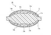
図12に示す回折光学素子100は、従来の回折光学素子の一例である。基材101は、屈折率がn(λ)である材料からなり、その表面にブレーズ状の回折格子形状102が形成されている。 A diffractive
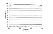
図13は、基材101の材料をシクロオレフィン系樹脂(日本ゼオン社製“ZEONEX”)として、回折格子深さdを0.95μmとした回折光学素子100の波長による1次回折効率の変化を示すグラフである。 FIG. 13 shows changes in the first-order diffraction efficiency depending on the wavelength of the diffractive
この1次回折効率は、波長500nmではほぼ100%に近くなるが、波長400nm及び波長700nmでは75%程度となり、波長による回折効率の変化(波長依存性)が顕著である。この回折光学素子を広い波長帯域(例えば、波長400nm〜700nm程度の可視光域等)で用いる撮像用途のレンズに適用すると、不要な回折光が発生し、フレアやゴーストとなって画像を劣化させたり、MTF(Modulation Transfer Function:変調伝達関数)特性を低下させたりする。特に、単レンズ両面や光学系の多面に回折格子形状を形成する場合は、不要な回折光の発生がより顕著となる。 The first-order diffraction efficiency is almost 100% at a wavelength of 500 nm, but is about 75% at a wavelength of 400 nm and a wavelength of 700 nm, and the change in diffraction efficiency depending on the wavelength (wavelength dependence) is remarkable. When this diffractive optical element is applied to a lens for imaging use that uses a wide wavelength band (for example, a visible light range of about 400 nm to 700 nm), unnecessary diffracted light is generated, resulting in flare and ghost, which degrades the image. Or reduce the MTF (Modulation Transfer Function) characteristic. In particular, when diffraction grating shapes are formed on both surfaces of a single lens or on multiple surfaces of an optical system, generation of unnecessary diffracted light becomes more significant.
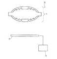
図14に示す回折光学素子110は、従来の回折光学素子の別の一例である。基材111の回折格子形状112が形成された面上に、基材111とは異なる屈折率及び屈折率分散を有する光学材料を、被覆膜113として塗布又は接合することにより、不要な回折光の発生を抑制できる。以下の文献には、この回折光学素子が、より具体的に開示されている。 A diffractive
特許文献1には、回折格子形状が形成された基材の屈折率と、回折格子形状を覆うように形成された被覆膜の屈折率を特定の条件に設定することにより、回折効率の波長依存性を低減する例が開示されている。また、特許文献2には、特許文献1と同様の屈折率条件で、MTF特性の波長依存性を低減する例が開示されている。 In Patent Document 1, the wavelength of the diffraction efficiency is set by setting the refractive index of the base material on which the diffraction grating shape is formed and the refractive index of the coating film formed so as to cover the diffraction grating shape to specific conditions. An example of reducing the dependency is disclosed.
特許文献3には、基材及び被覆膜の材料として、所定の屈折率条件を満足する樹脂やガラス等を組み合わせた材料を用いることによって、回折効率の波長依存性を低減する例が開示されている。 Patent Document 3 discloses an example in which the wavelength dependency of diffraction efficiency is reduced by using a material combining a resin, glass, or the like that satisfies a predetermined refractive index condition as a material for a base material and a coating film. ing.
特許文献4には、フルオレン誘導体を含有するエネルギー硬化型樹脂を用いることで同様の効果が得られることが開示されている。 Patent Document 4 discloses that the same effect can be obtained by using an energy curable resin containing a fluorene derivative.
回折光学素子110で用いられる材料は、大別すると樹脂又はガラスである。また、回折光学素子110の各部材の屈折率条件は、基本的には同様である。ここで、回折格子形状112が形成された基材111に、光学材料を被覆膜113として塗布、接合した場合、1次回折効率が100%となる回折格子深さd´は、下記数式2で与えられる。但し、n1(λ)は基材を構成する材料の屈折率、n2(λ)は被覆膜を構成する材料の屈折率であり、いずれも波長の関数である。 The material used in the diffractive
数式2の右辺が、ある波長帯域で一定値になれば、その波長帯域での回折効率の波長依存性がなくなることになる。この条件を満たし、かつ回折格子深さd´を小さくするには、|n1(λ)−n2(λ)|の値を大きく、すなわち、基材と被覆膜を高屈折率かつ低分散材料と低屈折率かつ高分散材料の組合せで構成すればよい。なお、この構成において回折格子深さd´は、数式1の回折格子深さdよりも大きくなる。 If the right side of Formula 2 becomes a constant value in a certain wavelength band, the wavelength dependence of the diffraction efficiency in that wavelength band is lost. In order to satisfy this condition and reduce the diffraction grating depth d ′, the value of | n1 (λ) −n2 (λ) | is increased, that is, the base material and the coating film are made of a high refractive index and low dispersion material. And a combination of a low refractive index and a high dispersion material. In this configuration, the diffraction grating depth d ′ is larger than the diffraction grating depth d of Equation 1.
一方、これらの回折光学素子の製造方法としては、いくつか提案されているが、例えば、特許文献5及び特許文献6では、不要な回折光の発生原因となる気泡を除去するために、塗布される光学材料を低粘度に限定したり、塗布後に振動を加えたりする製造方法が開示されている。
しかしながら、図12に示した回折光学素子は、回折効率に波長依存性があるため、ある広い波長帯域において不要な回折光が発生するという課題がある。また、図14に示した回折光学素子は、回折効率の波長依存性を低減し、不要な回折光の発生を抑制できるものの、回折光学素子の材料として、ガラスを用いると成形が難しく、樹脂を用いると回折効率及びその波長依存性が温度変化の影響を受けやすいという課題や、材料が制限されるため回折格子深さを大きくしなければならないという課題がある。回折格子深さが大きいと、成形が困難となるおそれがある。 However, the diffractive optical element shown in FIG. 12 has a problem that unnecessary diffraction light is generated in a wide wavelength band because the diffraction efficiency has wavelength dependency. The diffractive optical element shown in FIG. 14 can reduce the wavelength dependency of diffraction efficiency and suppress the generation of unnecessary diffracted light. However, if glass is used as the material of the diffractive optical element, it is difficult to mold the resin. When it is used, there is a problem that the diffraction efficiency and its wavelength dependency are easily affected by a temperature change, and there is a problem that the diffraction grating depth must be increased because the material is limited. If the diffraction grating depth is large, molding may be difficult.
本発明は、成形しやすい回折光学素子、その回折光学素子を含む撮像装置及びその回折光学素子の製造方法を提供する。 The present invention provides a diffractive optical element that is easy to mold, an imaging device including the diffractive optical element, and a method for manufacturing the diffractive optical element.
本発明の回折光学素子は、樹脂を含む第1材料からなり、かつ、回折格子形状に形成された面を含む基材と、樹脂を含む第2材料からなり、かつ、前記面の前記回折格子形状部分に接して配置された被覆膜とを含む回折光学素子であって、
前記第1材料及び前記第2材料から選ばれる少なくとも1つの材料は、無機粒子を含むコンポジット材料であることを特徴とする。The diffractive optical element of the present invention is made of a first material containing a resin and includes a base material including a surface formed in a diffraction grating shape, a second material containing a resin, and the diffraction grating on the surface. A diffractive optical element including a coating film disposed in contact with the shape part,
At least one material selected from the first material and the second material is a composite material containing inorganic particles.
本発明の撮像装置は、光学系と、前記光学系を通過した被写体からの光を受光する撮像素子と、前記撮像素子によって検出された情報から被写体像を生成する演算回路とを含む撮像装置であって、
前記光学系は、前記本発明の回折光学素子を含むことを特徴とする。An imaging apparatus of the present invention is an imaging apparatus including an optical system, an imaging element that receives light from a subject that has passed through the optical system, and an arithmetic circuit that generates a subject image from information detected by the imaging element. There,
The optical system includes the diffractive optical element of the present invention.
本発明の回折光学素子の製造方法は、樹脂を含む第1材料からなり、かつ、回折格子形状に形成された面を含む基材と、樹脂を含む第2材料からなり、かつ、前記回折格子形状を覆う被覆膜とを含む回折光学素子の製造方法であって、
前記回折格子形状に形成された面を含む前記基材を形成する工程と、
前記回折格子形状を覆うように、前記被覆膜を形成する工程とを含み、
前記第1材料及び前記第2材料から選ばれる少なくとも1つの材料は、無機粒子を含むコンポジット材料であることを特徴とする。The method for producing a diffractive optical element of the present invention includes a base material including a first material including a resin and a surface formed in a diffraction grating shape, a second material including a resin, and the diffraction grating. A method of manufacturing a diffractive optical element including a coating film covering a shape,
Forming the substrate including a surface formed in the diffraction grating shape;
Forming the coating film so as to cover the diffraction grating shape,
At least one material selected from the first material and the second material is a composite material containing inorganic particles.
本発明の回折光学素子は、回折格子形状に形成された面を含む基材と、前記回折格子形状を覆う被覆膜とを含む。そして、前記基材は樹脂を含む第1材料からなり、前記被覆膜は樹脂を含む第2材料からなり、前記第1材料及び前記第2材料から選ばれる少なくとも1つの材料は、無機粒子を含むコンポジット材料である。このような構成にすることによって、従来のガラス等を用いた場合に比べ成形性が向上する。また、被覆膜と基材との屈折率差が最適な値となるように、それぞれの材料に使用する樹脂や無機粒子を適宜選択することができる。これにより、従来の樹脂等を用いた場合に比べ材料選択の幅が拡がるため、例えば回折格子深さを浅くすることができる。よって、加工がより容易となる。 The diffractive optical element of the present invention includes a base material including a surface formed in a diffraction grating shape, and a coating film covering the diffraction grating shape. The substrate is made of a first material containing a resin, the coating film is made of a second material containing a resin, and at least one material selected from the first material and the second material is made of inorganic particles. It is a composite material containing. By adopting such a configuration, formability is improved as compared with the case of using conventional glass or the like. Moreover, resin and inorganic particle | grains used for each material can be suitably selected so that the refractive index difference of a coating film and a base material may become an optimal value. As a result, the range of material selection is broader than when a conventional resin or the like is used, so that the depth of the diffraction grating can be reduced, for example. Therefore, processing becomes easier.
前記無機粒子は、酸化ジルコニウム、酸化亜鉛及び酸化アルミニウムから選ばれる少なくとも1つからなることが好ましい。本発明の回折光学素子における回折効率の波長依存性をより低減できるからである。 The inorganic particles are preferably composed of at least one selected from zirconium oxide, zinc oxide, and aluminum oxide. This is because the wavelength dependency of the diffraction efficiency in the diffractive optical element of the present invention can be further reduced.
前記第1材料は、前記コンポジット材料であることが好ましく、この場合、前記コンポジット材料に占める前記無機粒子の体積含有率が、5体積%以上50体積%以下の範囲にあることが好ましい。より高い成形性が得られる上、比較的浅い回折格子深さで、回折効率の波長依存性の少ない回折光学素子を設計できるからである。 The first material is preferably the composite material. In this case, the volume content of the inorganic particles in the composite material is preferably in the range of 5% by volume to 50% by volume. This is because higher formability can be obtained and a diffractive optical element having a relatively shallow diffraction grating depth and less wavelength dependency of diffraction efficiency can be designed.
前記第1材料は、前記第2材料よりも屈折率及びアッベ数の高い材料又は屈折率及びアッベ数の低い材料であることが好ましい。このような第1材料を用いることによって、回折効率の波長依存性を低減できるからである。第1材料と第2材料とのd線屈折率の差は、0.03以上0.13以下の範囲、アッベ数の差は、8以上の範囲であれば、回折効率の波長依存性をより低減できる。 The first material is preferably a material having a higher refractive index and an Abbe number or a material having a lower refractive index and an Abbe number than the second material. This is because the wavelength dependence of diffraction efficiency can be reduced by using such a first material. If the difference in d-line refractive index between the first material and the second material is in the range of 0.03 to 0.13 and the difference in Abbe number is in the range of 8 or more, the wavelength dependence of the diffraction efficiency is further increased. Can be reduced.
前記第1材料及び前記第2材料から選ばれる少なくとも1つの材料は、赤外線領域の波長の光を吸収する材料又は紫外線領域の波長の光を吸収する材料であることが好ましい。別途、赤外線遮蔽効果又は紫外線遮蔽効果を有する部材を用いる必要がなくなるからである。 It is preferable that at least one material selected from the first material and the second material is a material that absorbs light having a wavelength in the infrared region or a material that absorbs light having a wavelength in the ultraviolet region. This is because it is not necessary to separately use a member having an infrared shielding effect or an ultraviolet shielding effect.
前記回折格子形状の溝の深さは、20μm以下であることが好ましい。溝の深さが20μm以下であれば、回折格子形状のピッチの間隔を細かくすることができるので、ピッチ数を増やすことができるからである。これにより、例えば本発明の回折光学素子をレンズに適用した場合、MTF特性の向上や色収差の低減等、光学素子の性能を向上させることができる。 The depth of the diffraction grating-shaped groove is preferably 20 μm or less. This is because if the groove depth is 20 μm or less, the pitch interval of the diffraction grating shape can be reduced, and the number of pitches can be increased. Thereby, for example, when the diffractive optical element of the present invention is applied to a lens, the performance of the optical element such as improvement of MTF characteristics and reduction of chromatic aberration can be improved.
また、本発明の回折光学素子は、前記被覆膜における前記回折格子形状側の反対面に配置され、かつ、第3材料からなる反射防止膜をさらに含むことが好ましい。回折光学素子に入射する光のうち、全反射する光を少なくすることができるので、回折効率をより高くすることができるからである。前記反射防止膜は、単層の膜であっても、複数層からなる膜であってもよい。前記第3材料は、前記第2材料よりも屈折率の低い材料であることがより好ましい。より反射光を低減できるからである。また、前記第3材料は、樹脂と、無機粒子(特に酸化シリコン)とを含む材料であることがより好ましい。回折効率の波長依存性をより低減できるからである。 Moreover, it is preferable that the diffractive optical element of the present invention further includes an antireflection film which is disposed on the surface opposite to the diffraction grating shape side of the coating film and is made of a third material. This is because the light that is totally reflected among the light incident on the diffractive optical element can be reduced, so that the diffraction efficiency can be further increased. The antireflection film may be a single layer film or a film composed of a plurality of layers. More preferably, the third material is a material having a lower refractive index than the second material. This is because the reflected light can be further reduced. The third material is more preferably a material containing a resin and inorganic particles (particularly silicon oxide). This is because the wavelength dependency of diffraction efficiency can be further reduced.
前記第1材料、前記第2材料及び前記第3材料から選ばれる少なくとも1つに含まれる無機粒子の平均粒径は、1nm以上100nm以下の範囲にあることが好ましい。無機粒子の粒子径が1nm以上100nm以下の範囲であれば、レーリー散乱のみとなり、コンポジット材料における分散性が向上し、透明性の高い材料となるからである。 The average particle diameter of the inorganic particles contained in at least one selected from the first material, the second material, and the third material is preferably in the range of 1 nm to 100 nm. This is because if the particle diameter of the inorganic particles is in the range of 1 nm to 100 nm, only Rayleigh scattering occurs, dispersibility in the composite material is improved, and a highly transparent material is obtained.
本発明の撮像装置は、光学系と、前記光学系を通過した被写体からの光を受光する撮像素子と、前記撮像素子によって検出された情報から被写体像を生成する演算回路とを含む撮像装置であって、前記光学系は、上述した回折光学素子を含む。本発明の撮像装置は、光学系に成形性のよい本発明の回折光学素子を含むので、製造コストの低減が可能となる。 An imaging apparatus of the present invention is an imaging apparatus including an optical system, an imaging element that receives light from a subject that has passed through the optical system, and an arithmetic circuit that generates a subject image from information detected by the imaging element. The optical system includes the diffractive optical element described above. Since the imaging device of the present invention includes the diffractive optical element of the present invention having good moldability in the optical system, the manufacturing cost can be reduced.
本発明の回折光学素子の製造方法は、樹脂を含む第1材料からなり、かつ、回折格子形状に形成された面を含む基材と、樹脂を含む第2材料からなり、かつ、前記回折格子形状を覆う被覆膜とを含む回折光学素子の製造方法であって、前記回折格子形状に形成された面を含む前記基材を形成する工程と、前記回折格子形状を覆うように、前記被覆膜を形成する工程とを含む。そして、前記第1材料及び前記第2材料から選ばれる少なくとも1つの材料は、樹脂と無機粒子とを含むコンポジット材料である。このような工程を含む製造方法によって、成形しやすい回折光学素子を提供できる。 The method for producing a diffractive optical element of the present invention includes a base material including a first material including a resin and a surface formed in a diffraction grating shape, a second material including a resin, and the diffraction grating. A method of manufacturing a diffractive optical element including a coating film covering a shape, the step of forming the base material including a surface formed in the diffraction grating shape, and the object to be covered so as to cover the diffraction grating shape. Forming a cover film. At least one material selected from the first material and the second material is a composite material containing a resin and inorganic particles. A diffractive optical element that can be easily molded can be provided by a manufacturing method including such steps.
また、前記被覆膜を形成する工程は、減圧下の雰囲気において、未硬化状態の樹脂を含む材料を、前記回折格子形状を覆うように配置して、前記雰囲気の圧力を上げることによって、前記回折格子形状と前記材料とを密着させて、前記樹脂を硬化させる工程を含むことが好ましい。被覆膜を回折格子形状の溝により密着させて形成できるからである。 Further, the step of forming the coating film includes arranging a material containing an uncured resin in an atmosphere under reduced pressure so as to cover the diffraction grating shape, and increasing the pressure of the atmosphere. It is preferable to include a step of bringing the diffraction grating shape and the material into close contact with each other and curing the resin. This is because the coating film can be formed in close contact with a diffraction grating-shaped groove.
また、前記第1材料は、前記第2材料よりも屈折率の低い材料であり、前記基材を形成する工程において、前記回折格子形状を模った型を用いて前記面を形成することが好ましい。第1材料が第2材料より屈折率が低い場合は、第1材料からなる基材の回折格子形状を模った型を、より形成しやすくなるので、前記回折格子形状のピッチ数を増やすことができるからである。これにより、回折格子形状による収差低減効果を大きくできる。 The first material is a material having a refractive index lower than that of the second material, and in the step of forming the base material, the surface may be formed using a mold imitating the diffraction grating shape. preferable. When the refractive index of the first material is lower than that of the second material, it is easier to form a mold that simulates the diffraction grating shape of the base material made of the first material, so the number of pitches of the diffraction grating shape is increased. Because you can. Thereby, the aberration reduction effect by a diffraction grating shape can be enlarged.
以下、図面を参照しながら、本発明の好ましい形態について説明する。なお、本発明は以下の実施形態に限定されるものではない。 Hereinafter, preferred embodiments of the present invention will be described with reference to the drawings. In addition, this invention is not limited to the following embodiment.
(実施形態1)
図1に、本発明の回折光学素子の一例として、両面に回折格子形状を形成したレンズ10の断面図を示す。レンズ10の基材11は、輪帯状の回折格子形状12aが形成された面11aと、面11aと反対側で、かつ輪帯状の回折格子形状12bが形成された面11bとを含む。そして、これらの回折格子形状12a,12bを覆うように被覆膜13a,13bがそれぞれ形成されている。(Embodiment 1)
FIG. 1 shows a cross-sectional view of a
回折格子形状12a及び回折格子形状12bは必ずしも同じ回折格子深さ、形状である必要はない。また、回折格子形状12a内の輪帯状のピッチは同じである必要はない。また、輪帯である必要はなく直線状、曲線状の回折格子形状やホログラフィック回折格子形状でも構わない。また被覆膜13a,13bのそれぞれの材料、及びそれぞれの厚みも同じである必要はない。基材11の形状は両面ともが凸面である必要はなく、凹面と凸面、両面凹面、両面平面、平面と凸面、平面と凹面等でもよい。また、回折格子形状は一方の片面のみに形成されていてもよい。 The diffraction grating shape 12a and the
本実施形態のレンズ10では、基材11は第1材料からなり、被覆膜13a,13bは第2材料からなる。第1材料及び第2材料は樹脂を含む。また、第1材料及び第2材料から選ばれる少なくとも1つは、樹脂と無機粒子とを含むコンポジット材料である。 In the
なお、前記コンポジット材料には樹脂及び無機粒子以外のものが含まれていてもよい。例えば、分散剤や硬化剤等が含まれていてもよい。樹脂及び無機粒子以外の材料の含有量は、通常、10体積%未満であり、1体積%未満であることが好ましい。 The composite material may contain a resin other than resin and inorganic particles. For example, a dispersant, a curing agent, or the like may be included. The content of materials other than the resin and the inorganic particles is usually less than 10% by volume, and preferably less than 1% by volume.
前記無機粒子は、平均粒子径が1nm以上100nm以下の範囲であることが好ましく、1nm以上40nm以下の範囲であることがより好ましい。なお、上記「平均粒子径が1nm以上100nm以下の範囲」とは、例えば、無機粒子全体を粒度分布計で測定したとき、粒度頻度分布の中心粒径が1nm〜100nmの範囲にあり、その平均粒子径を中心に頻度分布の50%以上が1nm〜100nmの範囲にあることを意味する。前記無機粒子の粒子径が光の波長よりも充分に小さいと、分散性がよく、前記コンポジット材料を屈折率のばらつきがない均一な媒体とみなすことができる。なお、光の波長の1/4以上、例えば無機粒子の平均粒子径が100nmを超えると、コンポジット材料中の無機粒子の散乱がミー散乱となるので、透明性が悪化する。また、無機粒子の平均粒子径が1nm未満であると、量子的な効果が発現する物質の場合、蛍光が生じる等といった光学性能に影響を及ぼすことがある。従って、前記無機粒子の粒子径が1nm以上100nm以下の範囲であれば、レーリー散乱のみとなり、コンポジット材料における分散性がよく、透明性の高い材料となる。また、蛍光等の付加的な光学性能が発現することもない。 The inorganic particles preferably have an average particle diameter in the range of 1 nm to 100 nm, and more preferably in the range of 1 nm to 40 nm. The above-mentioned “range where the average particle diameter is 1 nm or more and 100 nm or less” means, for example, when the whole inorganic particles are measured with a particle size distribution meter, the central particle diameter of the particle size frequency distribution is in the range of 1 nm to 100 nm, and the average This means that 50% or more of the frequency distribution centering on the particle diameter is in the range of 1 nm to 100 nm. When the particle diameter of the inorganic particles is sufficiently smaller than the wavelength of light, the dispersibility is good, and the composite material can be regarded as a uniform medium having no refractive index variation. In addition, when the wavelength of light is ¼ or more, for example, when the average particle diameter of the inorganic particles exceeds 100 nm, the scattering of the inorganic particles in the composite material becomes Mie scattering, so that the transparency is deteriorated. In addition, if the average particle size of the inorganic particles is less than 1 nm, the optical performance such as the generation of fluorescence may be affected in the case of a substance that exhibits a quantum effect. Therefore, when the particle diameter of the inorganic particles is in the range of 1 nm to 100 nm, only Rayleigh scattering is obtained, and the dispersibility in the composite material is good and the material is highly transparent. Further, additional optical performance such as fluorescence does not appear.
なお、前記無機粒子の平均粒子径は、TEM(Transmission Electron Microscope)撮影等による画像処理法で測定することができる。 The average particle diameter of the inorganic particles can be measured by an image processing method such as TEM (Transmission Electron Microscope) imaging.
コンポジット材料は、特定の材料からなる1種類の無機粒子のみを含んでいてもよいし、異なる材料からなる複数種の無機粒子を含んでいてもよい。 The composite material may contain only one kind of inorganic particles made of a specific material, or may contain a plurality of kinds of inorganic particles made of different materials.
前記無機粒子としては、例えば、酸化チタン、酸化タンタル、酸化亜鉛、酸化ジルコニウム、酸化アルミニウム、酸化イットリウム、酸化シリコン、酸化ニオブ、酸化セリウム、酸化インジウム、酸化スズ、酸化ハフニウム等の金属酸化物を用いることができる。無機粒子はこれらの酸化物のいずれか1つで形成されていてもよいし、これらの酸化物の複合酸化物で形成されていてもよい。また、無機粒子の材料としては窒化シリコン等の金属窒化物や炭化シリコン等の金属炭化物、ダイヤモンドやダイヤモンドライクカーボン等の光透過性の炭素系材料を用いてもよい。また、硫化硫黄や硫化スズ等の硫化物や、金、白金、銀、パラジウム、銅、アルミニウム等の金属、シリコンやゲルマニウム等の半導体材料を用いてもよい。これらの無機粒子を適宜組み合わせて用いることによって、コンポジット材料の屈折率及びアッベ数を調整できるので、広い波長範囲で高い回折効率をもつ回折光学素子となる。 Examples of the inorganic particles include metal oxides such as titanium oxide, tantalum oxide, zinc oxide, zirconium oxide, aluminum oxide, yttrium oxide, silicon oxide, niobium oxide, cerium oxide, indium oxide, tin oxide, and hafnium oxide. be able to. The inorganic particles may be formed of any one of these oxides, or may be formed of a composite oxide of these oxides. Further, as the material of the inorganic particles, a metal nitride such as silicon nitride, a metal carbide such as silicon carbide, or a light-transmitting carbon-based material such as diamond or diamond-like carbon may be used. Alternatively, sulfides such as sulfur sulfide and tin sulfide, metals such as gold, platinum, silver, palladium, copper, and aluminum, and semiconductor materials such as silicon and germanium may be used. By appropriately using these inorganic particles in combination, the refractive index and Abbe number of the composite material can be adjusted, so that a diffractive optical element having high diffraction efficiency in a wide wavelength range is obtained.
一方、樹脂としては熱可塑性樹脂、熱硬化性樹脂、光硬化性樹脂といった樹脂の中で、光透過性のよい樹脂を用いることができる。アクリル樹脂(例えば、ポリメタクリル酸メチル等)、エポキシ樹脂、ポリエステル樹脂(例えば、ポリエチレンテレフタレート、ポリブチレンテレフタレート、ポリカプロラクトン等)、ポリスチレン樹脂(例えば、ポリスチレン等)、ポリオレフィン樹脂(例えば、ポリプロピレン等)、ポリアミド樹脂(例えば、ナイロン等)、ポリイミド樹脂(例えば、ポリイミド、ポリエーテルイミド等)、ポリビニルアルコール樹脂、ブチラール樹脂、フルオレン系樹脂、酢酸ビニル樹脂等を用いてもよい。また、ポリカーボネート、液晶ポリマー、ポリフェニレンエーテル、ポリスルホン、ポリエーテルスルホン、ポリアリレート、非晶質ポリオレフィン等のエンジニアリングプラスティックを用いてもよい。また、これらの樹脂、高分子の混合体や共重合体を用いてもよい。また、これらの樹脂を変性したものを用いてもよい。 On the other hand, as the resin, a resin having good light transmittance can be used among resins such as a thermoplastic resin, a thermosetting resin, and a photocurable resin. Acrylic resin (for example, polymethyl methacrylate), epoxy resin, polyester resin (for example, polyethylene terephthalate, polybutylene terephthalate, polycaprolactone, etc.), polystyrene resin (for example, polystyrene), polyolefin resin (for example, polypropylene), Polyamide resin (for example, nylon), polyimide resin (for example, polyimide, polyetherimide, etc.), polyvinyl alcohol resin, butyral resin, fluorene resin, vinyl acetate resin, or the like may be used. Further, engineering plastics such as polycarbonate, liquid crystal polymer, polyphenylene ether, polysulfone, polyethersulfone, polyarylate, and amorphous polyolefin may be used. Further, a mixture or copolymer of these resins or polymers may be used. Moreover, you may use what modified | denatured these resin.
前記樹脂の中でも特に、アクリル樹脂、エポキシ樹脂、非晶質ポリオレフィン、ポリカーボネート樹脂、ポリイミド樹脂、ブチラール樹脂は透明性が高く、成形性も良好である。 Among these resins, acrylic resins, epoxy resins, amorphous polyolefins, polycarbonate resins, polyimide resins, and butyral resins have high transparency and good moldability.
前記コンポジット材料に占める前記無機粒子の種類及びその体積含有率を選択することによって、前記コンポジット材料の屈折率及びアッベ数を自由に制御することができる。例えば、前記コンポジット材料の屈折率は、マクスウェル−ガーネット理論に基づき、下記数式3により推定できる。但し、屈折率navはコンポジット材料の平均屈折率、npは無機粒子の屈折率、nmは樹脂の屈折率であり、Pはコンポジット材料に占める前記無機粒子の体積含有率である。また、前記無機粒子が光を吸収する場合や金属からなる場合には、複素屈折率として計算する。By selecting the kind of the inorganic particles in the composite material and the volume content thereof, the refractive index and Abbe number of the composite material can be freely controlled. For example, the refractive index of the composite material can be estimated by the following Equation 3 based on Maxwell-Garnet theory. However, the refractive index nav is the average refractive index of the composite material, np is the refractive index of the inorganic particles,nm is the refractive index of the resin, and P is the volume content of the inorganic particles in the composite material. Moreover, when the said inorganic particle absorbs light or consists of metals, it calculates as a complex refractive index.
また、前記コンポジット材料のアッベ数は、数式3を用いて、d線波長(587.6nm)、F線波長(486.1nm)、C線波長(656.3nm)の屈折率を算出することによって求めることができる。 The Abbe number of the composite material is calculated by calculating the refractive index of the d-line wavelength (587.6 nm), the F-line wavelength (486.1 nm), and the C-line wavelength (656.3 nm) using Equation 3. Can be sought.
なお、数式3の関係から、コンポジット材料の平均屈折率及びアッベ数は、無機粒子の体積含有率が増えるとともに、樹脂の屈折率及びアッベ数から無機粒子の屈折率及びアッベ数に近づくことがわかる。 From the relationship of Formula 3, it can be seen that the average refractive index and Abbe number of the composite material increase from the refractive index and Abbe number of the resin to the refractive index and Abbe number of the inorganic particle as the volume content of the inorganic particles increases. .
なお、この明細書において、「コンポジット材料の屈折率」とは、コンポジット材料を1つの屈折率を有する媒体とみなしたときの、実効的な屈折率を意味する。また、前記コンポジット材料の実際の屈折率は、基材11または被覆膜13a,13bの完成後に、例えばエリプソメトリ法、アベレス法、光導波路法、分光反射率法等を用いて測定することによって求めることができる。 In this specification, “refractive index of composite material” means an effective refractive index when the composite material is regarded as a medium having one refractive index. In addition, the actual refractive index of the composite material is measured by using, for example, an ellipsometry method, an Abeles method, an optical waveguide method, a spectral reflectance method, or the like after the
前記コンポジット材料が、シクロオレフィン系樹脂を主成分とする樹脂に無機粒子として酸化ジルコニウムを体積含有率50体積%で分散、混合した材料である場合、d線屈折率は1.796、アッベ数は41.9となる。酸化ジルコニウムは、d線屈折率が2.096、アッベ数が35.4であり、比較的高い屈折率と高いアッベ数とを備えた材料であり、酸化ジルコニウムの微粒子を樹脂に均一分散させることにより、高屈折率高アッベ数の材料を容易に実現することができる。樹脂はシクロオレフィン系樹脂に限定されないが、比較的アッベ数の大きな樹脂材料を組み合わせることが特に望ましい。また、このような高アッベ数を有する無機粒子としては、酸化アルミニウム、酸化イットリウム等もある。 When the composite material is a material in which zirconium oxide as inorganic particles is dispersed and mixed in a resin mainly composed of cycloolefin-based resin at a volume content of 50% by volume, the d-line refractive index is 1.796, and the Abbe number is 41.9. Zirconium oxide is a material having a d-line refractive index of 2.096 and an Abbe number of 35.4, a relatively high refractive index and a high Abbe number, and uniformly dispersing zirconium oxide fine particles in a resin. Thus, a material having a high refractive index and a high Abbe number can be easily realized. The resin is not limited to a cycloolefin resin, but it is particularly desirable to combine a resin material having a relatively large Abbe number. Examples of inorganic particles having such a high Abbe number include aluminum oxide and yttrium oxide.
一方、前記コンポジット材料が、ポリカーボネートを主成分とする樹脂に無機粒子として酸化亜鉛を体積含有率30体積%で分散、混合した材料である場合、d線屈折率は1.683、アッベ数は18.9である。酸化亜鉛は、d線屈折率が1.921、アッベ数が12.2であり、透明な無機材料としては中程度の屈折率と、比較的低いアッベ数を備えた材料である。このため酸化亜鉛微粒子を樹脂に均一に分散させたコンポジット材料により、低屈折率低アッベ数の材料を容易に実現することができる。樹脂はポリカーボネート樹脂に限定されないが、比較的アッベ数の小さな樹脂材料を組み合わせることが特に望ましい。 On the other hand, when the composite material is a material in which zinc oxide as inorganic particles is dispersed and mixed in a resin mainly composed of polycarbonate at a volume content of 30% by volume, the d-line refractive index is 1.683, and the Abbe number is 18 .9. Zinc oxide has a d-line refractive index of 1.921 and an Abbe number of 12.2, and is a material having a medium refractive index and a relatively low Abbe number as a transparent inorganic material. Therefore, a material having a low refractive index and a low Abbe number can be easily realized by a composite material in which zinc oxide fine particles are uniformly dispersed in a resin. The resin is not limited to polycarbonate resin, but it is particularly desirable to combine a resin material having a relatively small Abbe number.
第1材料がコンポジット材料の場合、回折格子形状12a,12bが形成された面11a,11bを含む基材11は、金型による成形で容易に大量生産できる。金型の加工の一例としては、金型素材の表面にメッキ膜を形成し、このメッキ膜にダイヤモンドバイトによる旋削加工を用いて回折格子形状12a,12bを模った型を形成する方法が挙げられる。前記コンポジット材料に、例えばカーボネート、シクロオレフィン系樹脂等の熱可塑性樹脂が配合されている場合は、射出成形によってコンポジット材料からなる基材11を容易に作製できる。また、前記コンポジット材料に、例えば光硬化性樹脂が配合されている場合は、紫外線や可視光を照射して光硬化性樹脂を硬化させ離型する方法、いわゆるフォトポリマー成形によって、コンポジット材料からなる基材11を容易に作製できる。その際用いる型は、石英等の紫外線や可視光を透過する材料にドライエッチング等で階段状の形状(回折格子形状12a,12bの反転形状)を形成するとよい。 When the first material is a composite material, the
これに対して、上述した特許文献1や特許文献2に開示されている従来のレンズは、基材又は被覆膜の構成材料としてガラスを用いているので、製造するのが難しい。ガラスの部材と樹脂の部材とを組み合わせたレンズのうち、基材を樹脂で、被覆膜をガラスで形成するのは困難である。これは、樹脂に数μmを越える厚さのガラスからなる被覆膜を形成すると、基材及び被覆膜のいずれかにクラックが発生するからである。また、ガラスからなる基材の形成は、樹脂からなる基材に比べて生産性が格段に劣る。最も生産性が期待できるのは金型によるプレス成形であるが、樹脂を用いた成形に比べて、金型の耐久性が1/10〜1/100しかなく、経済性及び量産性の観点から樹脂よりも極めて不利である。 On the other hand, the conventional lenses disclosed in Patent Document 1 and
また、上述した特許文献3に開示されている従来のレンズは、ポリカーボネートとポリスチレンを組み合わせることによって、特定の樹脂の組合せで回折効率の波長依存性をなくすもので、回折格子深さとして約280μmを必要としている。通常、数十μmを越える深さの回折格子形状の形成では、加工精度の高い金型加工が困難である。なぜなら、一般に金型加工はバイトを用いて行うが、回折格子深さが深いと加工量が増え、バイト先端が磨耗するため、加工精度が劣化する。同時に回折格子深さが深くなると格子ピッチを狭くすることができない。これは、回折格子深さが深くなると、先端の曲率半径が大きなバイトで金型を加工する必要があり、その結果、ある程度回折格子間のピッチを広げないと回折格子形状の加工ができないためである。これにより回折格子深さが深いほど回折格子形状の設計自由度が低減し、回折格子形状による収差低減効果がほとんどなくなってしまう。また、周辺温度の変化によりポリカーボネートとポリスチレンの屈折率差が変化するため、周辺温度の変化とともに回折効率の波長依存性が生じやすくなる。なお、金型加工の容易さと、レンズ性能面での回折格子形状12a,12bの寄与、および周辺温度に対する安定性を確保するには回折格子形状12a,12bの溝の深さを20μm以下にすることが望ましい。 In addition, the conventional lens disclosed in Patent Document 3 described above eliminates wavelength dependency of diffraction efficiency by combining a specific resin with a combination of polycarbonate and polystyrene, and the diffraction grating depth is about 280 μm. In need of. Usually, in the formation of a diffraction grating shape having a depth exceeding several tens of μm, it is difficult to mold with high processing accuracy. This is because die machining is generally performed using a cutting tool, but if the diffraction grating depth is deep, the amount of processing increases and the tip of the cutting tool wears, so that the processing accuracy deteriorates. At the same time, if the diffraction grating depth is increased, the grating pitch cannot be reduced. This is because as the diffraction grating depth increases, it is necessary to process the die with a tool having a large radius of curvature at the tip, and as a result, the diffraction grating shape cannot be processed unless the pitch between the diffraction gratings is widened to some extent. is there. As a result, the deeper the diffraction grating depth, the lower the degree of freedom in designing the diffraction grating shape, and the effect of reducing aberrations due to the diffraction grating shape is almost lost. Also, since the refractive index difference between polycarbonate and polystyrene changes due to changes in the ambient temperature, the wavelength dependence of diffraction efficiency tends to occur with changes in the ambient temperature. In order to secure the ease of mold processing, the contribution of the diffraction grating shapes 12a and 12b in terms of lens performance, and the stability to the ambient temperature, the depth of the grooves of the diffraction grating shapes 12a and 12b is set to 20 μm or less. It is desirable.
また、ダイヤモンドバイトによる旋削加工を用いて金型を加工し、この金型を用いた成形法で回折格子形状12a,12bを形成する場合、同一深さのブレーズ回折格子形状12a,12bであっても、ブレーズの傾斜方向により金型加工の難しさが異なるので、基材11に低屈折率低アッベ数の材料を用い、被覆膜13a,13bに高屈折率高アッベ数の材料を用いることが好ましい。金型加工が容易となり、加工精度が高くなるので、例えブレーズ深さを深くしても回折格子間のピッチを狭くすることができ、ピッチ数を増やすことができる。これにより、回折格子形状12a,12bによる収差低減効果を大きくできる。 Further, when a die is machined using a turning process using a diamond bit and the diffraction grating shapes 12a and 12b are formed by a molding method using this die, the blazed diffraction grating shapes 12a and 12b have the same depth. However, since the difficulty of mold processing differs depending on the blaze inclination direction, a material having a low refractive index and a low Abbe number is used for the
本実施形態のレンズ10ように、樹脂と無機粒子とを含むコンポジット材料を、基材11の材料及び被覆膜13a,13bの材料の少なくとも一方に用いることにより、製造が容易で光学性能に優れた回折光学素子が得られる。この場合、基材11及び被覆膜13a,13bは少なくとも樹脂を含む材料からなる。 As in the
本実施形態では、基材11がコンポジット材料の場合には、成形性の観点から、前記コンポジット材料に占める無機粒子の体積含有率が5体積%以上50体積%以下の範囲であることが好ましく、10体積%以上40体積%以下の範囲であることがより好ましい。無機粒子の種類によっては、体積含有率5体積%未満の微量の無機粒子を含むコンポジット材料であっても、良好な光学特性を示す場合もある。しかし、一般的には、無機粒子の体積含有率が5体積%未満であると、従来の樹脂の屈折率・分散特性から逸脱した特性を示すコンポジット材料を構成できず、回折格子深さを小さくできない。また、無機粒子の体積含有率が50体積%を超えると、コンポジット材料の光透過率が低下しその影響を無視できなくなる場合がある。前記範囲を満たすことにより、より高い成形性が得られる上、比較的浅い回折格子深さで、回折効率の波長依存性の少ない回折光学素子を設計できる。 In the present embodiment, when the
前記コンポジット材料は、熱膨張係数や、屈折率の温度依存性について、樹脂と無機粒子の中間的な物性値を有する。このため、前記第1材料及び前記第2材料が樹脂である場合に、しばしば問題となる光学性能の温度依存性が低減され、信頼性、光学安定性の面で樹脂より格段に優れる。無機粒子は、一般的に、樹脂に比べて、熱膨張係数や、屈折率の温度依存性が小さいためである。 The composite material has intermediate physical properties between resin and inorganic particles with respect to the coefficient of thermal expansion and the temperature dependence of the refractive index. For this reason, when the first material and the second material are resins, the temperature dependency of optical performance, which is often a problem, is reduced, and the reliability and optical stability are far superior to those of resins. This is because inorganic particles generally have a smaller coefficient of thermal expansion and temperature dependency of refractive index than resins.
また、第2材料がコンポジット材料の場合には、ハードコート効果がある。すなわち、無機粒子を含み、表面が固い膜で保護されることにより、信頼性が向上し、かつ表面に傷がつきにくくなる。 When the second material is a composite material, there is a hard coat effect. That is, by including inorganic particles and protecting the surface with a hard film, the reliability is improved and the surface is hardly damaged.
また、第1材料が熱可塑性樹脂を含み、射出成形により回折格子形状12a,12bが形成された場合には、樹脂に無機粒子を分散させることで複屈折の発生を抑制できる効果がある。これは、無機粒子により射出成形時の樹脂の配向が妨げられるので、光学的な等方性が維持されるためである。 In addition, when the first material contains a thermoplastic resin and the diffraction grating shapes 12a and 12b are formed by injection molding, there is an effect that the generation of birefringence can be suppressed by dispersing inorganic particles in the resin. This is because the optical isotropy is maintained because the inorganic particles prevent the orientation of the resin during injection molding.
また、第1材料及び第2材料から選ばれる少なくとも1つの材料は、赤外線領域の波長の光を吸収する材料であることが好ましい。赤外線遮蔽効果を有する回折光学素子を容易に得ることができるからである。この場合、CCD(Charge Coupled Device)、CMOS(Complementary Metal-oxide Semiconductor)等の赤外線の遮蔽を必要とする撮像素子やセンサと組み合わせて使用する際、別途赤外線カットフィルタを使用する必要がなくなる。前記赤外線領域の波長の光を吸収する材料とは、例えば赤外線領域の波長の光を吸収する物質を含有する材料、例えば、銅イオン等の金属イオンの錯塩を混入した樹脂や、近赤外波長領域に吸収を有するシアニン色素等の染料を溶解させた樹脂、あるいは酸化スズインジウム(ITO)等からなる無機粒子を含有する材料であればよい。 In addition, at least one material selected from the first material and the second material is preferably a material that absorbs light having a wavelength in the infrared region. This is because a diffractive optical element having an infrared shielding effect can be easily obtained. In this case, when using in combination with an image sensor or sensor that needs to shield infrared rays, such as a CCD (Charge Coupled Device) or a CMOS (Complementary Metal-oxide Semiconductor), it is not necessary to use an infrared cut filter. The material that absorbs light having a wavelength in the infrared region is, for example, a material containing a substance that absorbs light having a wavelength in the infrared region, such as a resin mixed with a complex salt of a metal ion such as copper ion, or a near-infrared wavelength. Any material containing inorganic particles made of a resin in which a dye such as a cyanine dye having absorption in a region is dissolved or indium tin oxide (ITO) may be used.
また、第1材料及び第2材料から選ばれる少なくとも1つの材料は、紫外線領域の波長の光を吸収する材料であることが好ましい。紫外線遮蔽効果を有する回折光学素子を容易に得ることができるからである。前記紫外線を吸収する材料としては、例えば酸化チタン、酸化亜鉛、酸化セリウム、酸化タングステン等の無機粒子を適量分散させた材料であればよい。この場合、可視光領域の透明性を確保しながら紫外線領域の光を吸収させることができるため、耐光性確保や、樹脂からの不要な蛍光の発生を阻止できる。 In addition, at least one material selected from the first material and the second material is preferably a material that absorbs light having a wavelength in the ultraviolet region. This is because a diffractive optical element having an ultraviolet shielding effect can be easily obtained. The material that absorbs ultraviolet rays may be any material in which an appropriate amount of inorganic particles such as titanium oxide, zinc oxide, cerium oxide, and tungsten oxide is dispersed. In this case, since light in the ultraviolet region can be absorbed while ensuring transparency in the visible light region, it is possible to ensure light resistance and prevent generation of unnecessary fluorescence from the resin.
なお、本発明の回折光学素子は、実施形態1のレンズ10に限定されるものではなく、空間ローパスフィルターや偏光ホログラム等、回折格子形状が用いられている光学デバイスに広く適用できるものである。特に、可視波長全域(400〜700nm)で第1材料の屈折率が第2材料の屈折率より大きい場合や、可視波長全域(400〜700nm)で第1材料の屈折率が第2材料の屈折率より小さい場合に、回折効率の波長依存性をより低減できる。 The diffractive optical element of the present invention is not limited to the
被覆膜13a及び被覆膜13bから選ばれる少なくとも1つは、回折格子形状12a,12b側とは反対側の表面が、ナノレベルの凹凸を有する反射防止形状であることが好ましい。光の反射をより軽減できるからである。この表面形状は、例えば、型による転写工法(ナノインプリント)等で容易に形成することができる。 It is preferable that at least one selected from the
(実施形態2)
次に、本発明の実施形態2に係る回折光学素子について説明する。なお、レンズの構成やコンポジット材料、製造上や性能上の効果等の説明について、実施形態1と重複する内容は省略する。(Embodiment 2)
Next, a diffractive optical element according to
図2は、本発明の回折光学素子の一例であるレンズ20の断面図である。本実施形態のレンズ20は、上述したレンズ10の構成要素に加え、被覆膜13aにおける回折格子形状12a側の反対面に配置された反射防止膜14aと、被覆膜13bにおける回折格子形状12b側の反対面に配置された反射防止膜14bとをさらに含む。これにより、上述したレンズ10と同様の効果を発揮させることができる上、レンズ20に入射した光のうち、全反射する光を少なくすることができるので、回折効率を高くすることができる。 FIG. 2 is a cross-sectional view of a
反射防止膜14a,14bはそれぞれ同じ材料である必要はなく、樹脂、または樹脂と無機粒子とのコンポジット材料のいずれか、あるいは真空蒸着等で形成された無機薄膜でもよい。 The
レンズ20の使用波長帯域のほぼ中央の波長λcでの被覆膜13a(13b)の屈折率をncとすると、その被覆膜13a(13b)上に形成される反射防止膜14a(14b)の屈折率がncの平方根であって膜厚がλc/4ncのときに垂直光に対して反射率がほぼ0となる。一方で反射防止膜14a(14b)がない場合、空気中から被覆膜13a(13b)、あるいは逆に被覆膜13a(13b)から空気中に抜ける光線に対して片面で{(nc−1)/(nc+1)}2の反射損失を生じる。なお、反射防止膜14a(14b)を付加した際の反射率は、反射防止膜14a(14b)の膜厚や屈折率が理想値からずれると0にはならないが、反射防止膜14a(14b)の屈折率が被覆膜13a(13b)よりも低ければ、反射防止膜14a(14b)がない場合の反射率、すなわち、{(nc−1)/(nc+1)}2よりも反射率が増えることはない。従って、反射防止膜14a(14b)の膜厚によらず、反射低減効果を有する。If the refractive index of the approximate center of the
反射防止膜14a,14bとしては、真空蒸着等で無機材料の単層膜や多層膜を形成してもよい。また、反射防止膜14a,14bは、前記コンポジット材料を用いることが好ましい。なぜなら製造が容易であるとともに、基材11、及び被覆膜13a,13bの少なくともいずれかはコンポジット材料であるので、これらと反射防止膜14a,14bの熱膨張率を近くすることができ、周辺温度に対する特性安定性が向上し、クラックや膜の剥離が起こりにくくなるためである。前記コンポジット材料中の無機粒子として酸化シリコンを用いると光透過性に優れる上、酸化シリコンは無機材料として屈折率が低く、アッベ数が高いので好ましい(d線屈折率1.456、アッベ数68.4)。この場合、広い波長帯域で反射防止効果を得ることができる。 As the
以下、実施形態2のレンズ20の好適な製造方法について説明する。図3,4,5に、上記製造方法を工程別に表した断面図を示す。 Hereinafter, a preferred method for manufacturing the
まず、図3Aに示すように、回折格子形状12a,12b(図2参照)を模った型31a,31bを用意する。そして、図3Bに示すように、真空注入ノズル32(図3A参照)から、型31a,31bに未硬化状態の第1材料33を流し入れて充填する。そして、図3Cに示すように、型31a,31bを外して、回折格子形状12a,12bが形成された面を含む基材11を形成する。なお、第1材料からなる基材11を形成する工程は、型を用いた成形プロセスに限定されないが、例えば第1材料が熱可塑性樹脂を主成分としている場合は射出成形、第1材料が光硬化性樹脂を主成分としている場合はフォトポリマー成形等を用いればよい。 First, as shown in FIG. 3A,
次に、図4Aに示すように、真空注液ノズル42,43を備えた気密容器41の内部に基材11を設置し、気密容器41の内部を減圧する。気密容器41内の圧力は、真空蒸着やCVD等の真空プロセスで求められるほど低くする必要はない。例えば、1Paから5000Pa程度の圧力で十分に効果が得られ、100Pa以下が好ましい。 Next, as shown in FIG. 4A, the
次に、図4Bに示すように、減圧された気密容器41内において、真空注液ノズル42から、第2材料からなる被覆膜13aを形成するための塗液44aを基材11の回折格子形状12aが形成された面に塗布する。そして、気密容器41内の圧力を減圧前の圧力に戻すことによって、塗液44a内から気泡を除去して回折格子形状12aの微細部分に塗液44aを隙間なく密着させて、被覆膜13a(図4C参照)を形成する。次に、図4Cに示すように、基材11を反転させて、気密容器41の内部を減圧し、真空注液ノズル42から、第2材料からなる被覆膜13bを形成するための塗液44bを基材11の回折格子形状12bが形成された面に塗布する。そして、被覆膜13aと同様に、気密容器41内の圧力を上げて、被覆膜13bを形成する。 Next, as shown in FIG. 4B, the
さらに、気密容器41の内部を減圧して、図5Aに示すように、真空注液ノズル43から、第3材料からなる反射防止膜14bを形成するための塗液45bを、被覆膜13bが形成された面に塗布する。そして、気密容器41内の圧力を減圧前の圧力に戻すことによって、塗液45b内から気泡を除去して被覆膜13bに密着させて、反射防止膜14b(図5B参照)を形成する。次に、図5Bに示すように、基材11を反転させて、気密容器41の内部を減圧し、真空注液ノズル43から、第3材料からなる反射防止膜14aを形成するための塗液45aを、被覆膜13aが形成された面に塗布する。そして、反射防止膜14bと同様に、気密容器41内の圧力を上げて、反射防止膜14aを形成し、図5Cに示すレンズ20が完成する。 Further, the inside of the
被覆膜13a,13bを形成する工程においては、減圧下の雰囲気において、第2材料からなる被覆膜13a,13bを形成するための塗液44a,44bを回折格子形状12a,12bの表面に配置する工程と、前記雰囲気の圧力を増大させることによって塗液44a,44bを回折格子形状12a,12bに隙間なく密着させる工程とを含めばよい。このような方法を用いることによって、基材11の表面の回折格子形状12a,12bの溝と被覆膜13a,13bとの間に隙間がなく、被覆膜13a,13b内に気泡の残存がないレンズ20を形成できる。また、被覆膜13a,13b及び反射防止膜14a,14bを形成する工程においては、スピンコートやディップコート等の塗布を用い、その後、加熱、光硬化、自然硬化等で硬化させる方法を用いてもよい。 In the step of forming the
第1材料及び第2材料は、少なくとも一方の材料がコンポジット材料であればよく、いずれの材料もコンポジット材料であることが好ましい。コンポジット材料の調製方法に限定はなく、物理的な方法で調製してもよいし化学的な方法で調製してもよい。例えば、以下の(1)〜(4)のいずれかの方法によりコンポジット材料を調製してもよい。 As for the first material and the second material, at least one of the materials may be a composite material, and any of the materials is preferably a composite material. The method for preparing the composite material is not limited, and it may be prepared by a physical method or a chemical method. For example, the composite material may be prepared by any of the following methods (1) to (4).
(1)樹脂または樹脂を溶解した溶液と1次粒径が1μm未満のサイズである無機粒子とを、機械的・物理的に混合する方法。 (1) A method of mechanically and physically mixing a resin or a resin-dissolved solution and inorganic particles having a primary particle size of less than 1 μm.
(2)樹脂の原料(単量体やオリゴマー等)と1次粒径が1μm未満のサイズである無機粒子とを、機械的・物理的に混合して混合物を得た後、樹脂の原料を重合する方法。重合は、混合物をレンズに塗布した後に行ってもよいし、塗布する前に行ってもよい。 (2) A resin raw material (monomer, oligomer, etc.) and inorganic particles having a primary particle size of less than 1 μm are mechanically and physically mixed to obtain a mixture. How to polymerize. The polymerization may be performed after the mixture is applied to the lens, or may be performed before the application.
(3)樹脂または樹脂を溶解した溶液と無機粒子の原料とを混合した後に無機粒子の原料を反応させ、樹脂中で無機粒子を形成する方法。 (3) A method of forming inorganic particles in a resin by reacting a raw material of inorganic particles after mixing a resin or a resin-dissolved solution and a raw material of inorganic particles.
(4)樹脂の原料(単量体やオリゴマー等)と無機粒子の原料とを混合した後、無機粒子の原料を反応させて無機粒子を合成する工程と、樹脂の原料を重合して樹脂を合成する工程とを行う方法。 (4) After mixing the resin raw material (monomer, oligomer, etc.) and the inorganic particle raw material, reacting the inorganic particle raw material to synthesize the inorganic particles; and polymerizing the resin raw material to obtain the resin And a process of synthesizing.
以上のうち、(1)及び(2)の方法では、予め形成された様々な無機粒子を用いることができ、汎用の分散装置によってコンポジット材料を調製できるという利点がある。 Among the above, the methods (1) and (2) have an advantage that various inorganic particles formed in advance can be used, and a composite material can be prepared by a general-purpose dispersion apparatus.
一方、(3)及び(4)の方法では、化学的な反応を行うことが必要であるため、材料に制限がある。しかし、これらの方法は原料を分子レベルで混合し、無機粒子の分散性を高めることができるという利点を有する。 On the other hand, in the methods (3) and (4), since it is necessary to perform a chemical reaction, there are limitations on materials. However, these methods have the advantage that the raw materials can be mixed at the molecular level to increase the dispersibility of the inorganic particles.
上述の方法において、無機粒子または無機粒子の原料と、樹脂または樹脂の原料とを混合する順序に特に限定はなく、好ましい順序を適宜選択すればよい。例えば、1次粒径が実質的に1nm〜100nmの範囲のサイズである無機粒子を分散した溶液に、樹脂、樹脂の原料、またはそれらを溶解した溶液を加えて機械的・物理的に混合してもよい。 In the above-described method, the order of mixing the inorganic particles or the raw material of the inorganic particles and the resin or the raw material of the resin is not particularly limited, and a preferable order may be appropriately selected. For example, a resin, a raw material of resin, or a solution in which they are dissolved is added to a solution in which inorganic particles whose primary particle size is substantially in the range of 1 nm to 100 nm is dispersed, and mechanically and physically mixed. May be.
また、第3材料は、特に限定されないが、第2材料よりも屈折率が低いことが好ましく、例えば、樹脂と無機粒子とを含む材料を用いればよい。 The third material is not particularly limited, but preferably has a refractive index lower than that of the second material. For example, a material containing a resin and inorganic particles may be used.
以下、第2材料として前記コンポジット材料を用いた場合の被覆膜13a,13bの形成方法の一例について説明する。被覆膜13a,13bは、コンポジット材料を形成するための物質を含む混合物(例えば、塗液)を用いて形成できる。この混合物(塗液)は、樹脂または樹脂の原料と、無機粒子と、溶媒(分散媒)とを含む。また、溶媒を含まない混合物を用いて被覆膜13a,13bを形成してもよい。この場合、熱可塑性樹脂を用い、昇温によって低粘度化させた混合物を用いるか、あるいは膜状の混合物を用いればよい。塗液は、例えば、以下の(1)〜(4)のいずれかの方法で調製できる。 Hereinafter, an example of a method of forming the
(1)コンポジット材料を溶剤によって希釈して塗液を調製する方法。この塗液を用いる場合、塗液を塗布したのちに溶剤を除去する。 (1) A method of preparing a coating liquid by diluting a composite material with a solvent. When this coating liquid is used, the solvent is removed after the coating liquid is applied.
(2)樹脂の単量体やオリゴマー、低分子量体等と無機粒子とを混合して塗液を調製する方法。この塗液を用いる場合、単量体やオリゴマー、低分子量体等の原料を反応させて樹脂を合成することが必要となる。 (2) A method of preparing a coating liquid by mixing resin monomers, oligomers, low molecular weight substances and the like and inorganic particles. When this coating solution is used, it is necessary to synthesize a resin by reacting raw materials such as monomers, oligomers, and low molecular weight substances.
(3)無機粒子の原料と樹脂と溶媒とを混合して塗液を調製する方法。この塗液を用いる場合、塗液を塗布したのちに無機粒子の原料をゾルゲル法等によって反応させて塗膜中で無機粒子を合成する。 (3) A method of preparing a coating liquid by mixing a raw material of inorganic particles, a resin, and a solvent. In the case of using this coating liquid, after applying the coating liquid, the inorganic particles are reacted by a sol-gel method or the like to synthesize inorganic particles in the coating film.
(4)加温して低粘度化した樹脂に無機粒子を分散させて塗液を調製する方法。この方法では、塗膜の温度が低下することによって塗膜が固化し、被覆膜13a,13bが形成される。 (4) A method of preparing a coating liquid by dispersing inorganic particles in a resin whose temperature has been lowered by heating. In this method, the coating film is solidified by lowering the temperature of the coating film, and the
これらの方法は、樹脂や無機粒子の材質や、塗布方法等に応じて適宜選択すればよい。なお、必要に応じて、塗液は、架橋剤、重合開始剤、分散剤等を含んでいてもよい。 These methods may be appropriately selected according to the material of the resin or inorganic particles, the coating method, and the like. In addition, the coating liquid may contain the crosslinking agent, the polymerization initiator, the dispersing agent, etc. as needed.
この混合物を回折格子形状12a,12bの表面に配置する方法に限定はなく、例えば公知の方法を適用できる。具体的にはディスペンサ等の注液ノズルを用いた塗布、インクジェット法等の噴射塗布、スピンコーティング等の回転による塗布、印刷等のスキージングによる塗布、転写等を適用してもよい。このような方法は既存の設備を用いて行うことができる。 There is no limitation on the method of disposing the mixture on the surfaces of the diffraction grating shapes 12a and 12b, and for example, a known method can be applied. Specifically, application using a liquid injection nozzle such as a dispenser, spray application such as an inkjet method, application by rotation such as spin coating, application by squeezing such as printing, transfer, or the like may be applied. Such a method can be performed using existing equipment.
塗液を塗布したのち、溶媒を除去することによって被覆膜13a,13bを形成できる。なお、塗液が樹脂の材料(単量体やオリゴマー等)や無機粒子の材料を含む場合、必要に応じて塗布後にそれらを反応させて樹脂や無機粒子を合成してもよい。また、塗液を塗布することによって形成された膜を硬化させて被覆膜13a,13bを形成してもよい。硬化処理は、光硬化、熱硬化、乾燥処理等で行うことができる。 After applying the coating liquid, the
以下、被覆膜13a,13b及び反射防止膜14a,14bを形成する別の方法を、図6,7を用いて説明する。 Hereinafter, another method for forming the
図6Aに示すように、気密容器51の内部に回折格子形状12a,12bが形成された面を含む基材11を設置し、気密容器51の内部を減圧する。また、第2材料からなる被覆膜13a,13bを形成するための塗膜53a,53bが形成された転写プレート52a,52bを準備する。 As shown in FIG. 6A, the
次に、図6Bに示すように、減圧された気密容器51内において、転写プレート52a,52bに塗布された塗膜53a,53bを、減圧下で基材11表面の回折格子形状12a,12bに密着させて転写する。次に、図6Cに示すように、気密容器51の内部の圧力を減圧前の圧力に戻すことによって、塗膜53a,53bに含まれる溶媒を除去して被覆膜13a,13bを得る。 Next, as shown in FIG. 6B, the
さらに、図7Aに示すように、第3材料からなる反射防止膜14a,14bを形成するための塗膜55a,55bが形成された転写プレート54a,54bを準備し、図7Bに示すように、転写プレート54a,54bを被覆膜13a,13bが形成された面に密着させることによって塗膜55a,55bを転写する。最後に、図7Cに示すように、大気下で塗膜55a,55bに含まれる溶媒を除去して反射防止膜14a,14bを形成し、レンズ20が完成する。 Furthermore, as shown in FIG. 7A,
塗膜53a,53b,55a,55bを形成する際は、例えば転写プレート52a,52b,54a,54bへスピンコーティング等の方法で塗布すれば膜厚の調整が可能となる。膜厚を数十μm程度の薄い膜にしておけば、塗膜53a,53b,55a,55b内からの気泡の除去がさらに容易となる。転写プレート52a,52b,54a,54bを密着させる際には、適宜圧力を加えて押し付けてもよい。 When the
上述した被覆膜13a,13b及び反射防止膜14a,14bを形成する工程は、比較的低温で行うことができる。そのため、低温プロセスが求められるレンズ等の回折光学素子を製造する場合に特に好ましい。 The process of forming the
以下、上述したレンズ20の製造方法で用いる好適な製造装置について説明する。図8は、上記製造装置を示す構成図である。 Hereinafter, a suitable manufacturing apparatus used in the method for manufacturing the
製造装置61は、気密容器62と、基材11を保持する基板保持ステージ63と、基板回転機構64と、真空注液ノズル65a,65bと、真空注液器(ヘッド)66a,66bと、塗液タンク67a,67bと、圧力制御バルブ68と、制御装置69とを含む。 The
気密容器62は、減圧状態を保持できる容器であり、真空ポンプ等の減圧装置(図示せず)が接続されている。基板保持ステージ63は、基板回転機構64により回転させることが可能である。真空注液ノズル65aと、真空注液器(ヘッド)66aと、塗液タンク67aとは、被覆膜13a,13bを形成する塗布装置を構成し、塗液タンク67a内には被覆膜13a,13bを形成するための塗液が配置される。また、真空注液ノズル65bと、真空注液器(ヘッド)66bと、塗液タンク67bとは、反射防止膜14a,14bを形成する塗布装置を構成し、塗液タンク67b内には反射防止膜14a,14bを形成するための塗液が配置される。圧力制御バルブ68は気密容器62内の圧力を調整する。気密容器62と前記減圧装置と圧力制御バルブ68とは、圧力調整装置を構成する。これらの装置は制御装置69によって制御される。 The
製造装置61を用いて、レンズ20を製造する方法の一例を説明する。まず、回折格子形状12a,12bの形成された面を含む基材11を基板保持ステージ63に固定する。固定方法は公知の方法、例えば接着や粘着剤による貼り付け、治具による固定、静電気による固定、あるいは真空チャックでもよい。真空チャックの場合はチャック内の圧力を、気密容器62内の圧力よりも低くする必要がある。 An example of a method for manufacturing the
次に、前記減圧装置と圧力制御バルブ68によって気密容器62を減圧したのち、真空注液ノズル65aと、真空注液器(ヘッド)66aとによって、基材11の回折格子形状12aが形成された面上に塗液を塗布する。このとき、基板回転機構64によって基板保持ステージ63を低速で回転させながら塗液を均一に塗布する。次に基板回転機構64によって基材11を高速で回転することによって、前記面上に配置された余分な塗液を除去する。そして、気密容器62内の減圧を解除して塗液の硬化処理を行い、被覆膜13aが形成される。これらの減圧プロセス、塗布プロセス、減圧解除プロセスといった一連のプロセスは制御装置69によって制御される。次に、基材11を反転させて、被覆膜13aと同様に、被覆膜13bを基材11の回折格子形状12bが形成された面上に形成する。 Next, after reducing the pressure of the
次に、前記減圧装置と圧力制御バルブ68によって気密容器62を減圧したのち、真空注液ノズル65bと、真空注液器(ヘッド)66bとによって、基材11の被覆膜13aが形成された面上に塗液を塗布する。このとき、基板回転機構64によって基板保持ステージ63を低速で回転させながら塗液を均一に塗布する。次に基板回転機構64によって基材11を高速で回転することによって、前記面上に配置された余分な塗液を除去する。そして、気密容器62内の減圧を解除して塗液の硬化処理を行い、反射防止膜14aが形成される。次に、基材11を反転させて、反射防止膜14aと同様に、反射防止膜14bを基材11の被覆膜13bが形成された面上に形成し、レンズ20が完成する。 Next, after the
製造装置61は、例えば被覆膜13a,13bを形成する第2材料がコンポジット材料である場合、上記コンポジット材料を形成するための物質を含む塗液を減圧下で所定の位置に塗布するための塗布装置と、塗液の塗布を行う際の雰囲気の圧力を減圧するための圧力調整装置とを備えればよい。前記塗布装置には、上述した塗布方法を実施するための装置を適用でき、例えば真空注液装置や、スピンコーティング装置、スクリーン印刷装置、ディスペンサ装置、インクジェット装置等を用いることができる。また、圧力調整装置には、公知の装置を適用でき、例えば気密状態を解除可能な気密容器と、気密容器に接続された減圧装置とを備える装置を適用できる。 For example, when the second material forming the
(実施形態3)
図9に、本発明の撮像装置の一例である撮像装置70の構成図を示す。(Embodiment 3)
FIG. 9 shows a configuration diagram of an
図9に示すように、本実施形態の撮像装置70は、上述した実施形態1及び2から選ばれた1つの形態に係るレンズを含む光学系71と、撮像素子72と、撮像素子72により検出された情報から被写体像を形成する演算回路73とを備える。 As shown in FIG. 9, the
撮像装置70では、被写体(図示せず)からの光が光学系71で集光され、撮像素子72上に結像される。そして、撮像素子72で受光された光が電気信号に変換され、演算回路73でカラー合成等の処理がなされ、適当な表示手段を接続することにより、画像として表示される。 In the
従来、カラー画像用途の撮像素子として、各画素にベイヤー配列等の特定の規則で緑、赤、青の色フィルタを配列し、隣接する画素による演算でカラー画像を得るものが知られている。 2. Description of the Related Art Conventionally, as an image sensor for use in a color image, an image sensor is known in which green, red, and blue color filters are arranged for each pixel according to a specific rule such as a Bayer arrangement, and a color image is obtained by calculation using adjacent pixels.
このようなカラー画像を得る場合には、2〜3枚程度の非球面レンズを光軸上に配列した光学系を用いるのが一般的であった。これは、1枚の非球面レンズでは色収差、すなわち波長による集光特性のずれを解消することができないため、解像度の高いカラー画像を得ることが困難となるためである。 In order to obtain such a color image, it is common to use an optical system in which about 2 to 3 aspheric lenses are arranged on the optical axis. This is because it is difficult to obtain a color image with high resolution because a single aspherical lens cannot eliminate the chromatic aberration, that is, the shift in the condensing characteristic due to the wavelength.
一方、本実施形態の撮像装置70では、屈折作用に加えて、回折作用をも合わせ持つ1枚のレンズからなる光学系71を用いているため、1枚のレンズで高い解像度を有するカラー画像を得ることが可能である。 On the other hand, in the
したがって、本実施形態の撮像装置70は、薄型及び小型化が可能になるとともに、光学系71に含まれるレンズ枚数を削減できるため各レンズの位置決め調整工程が簡略化し、生産性、経済性に優れる撮像装置70とすることができる。この撮像装置70は、携帯電話用、車載用、監視用あるいは医療用のカメラとして特に好適である。 Therefore, the
なお、本実施形態では、1枚のレンズで構成した撮像装置70を説明したが、複数枚のレンズからなる光学系の一部に、本発明の回折光学素子を組み入れた撮像装置としてもよい。この場合は、レンズ枚数を削減できるので有用である。 In the present embodiment, the
また、複数レンズからなる撮像レンズ系の1面に、一般的な回折格子形状を形成し、色収差を低減することが最近行われている。その場合、不要な回折光によるフレアやゴーストが発生しないように回折輪帯数は多くしないようにしているが、周辺に比べて輝度の高い被写体を撮影する場合には、本発明の回折光学素子を組み入れると、フレアやゴーストが発生せず有用である。 Further, it has recently been practiced to reduce the chromatic aberration by forming a general diffraction grating shape on one surface of an imaging lens system composed of a plurality of lenses. In that case, the number of diffracting ring zones is not increased so that flare and ghost due to unnecessary diffracted light do not occur, but the diffractive optical element of the present invention is used when photographing a subject with higher brightness than the surroundings. Incorporating is useful with no flare or ghosting.
また、本実施形態では、一対のレンズ及び撮像素子72からなる撮像装置70を例に説明したが、これを複数対、あるいは並列に配置した複眼型撮像装置としてもよい。この場合は複数画像を合成処理できる演算回路を用いればよい。 In the present embodiment, the
以下、本発明の回折光学素子の実施例について説明する。 Examples of the diffractive optical element of the present invention will be described below.
(実施例1)
実施例1は、上述した実施形態1のレンズ10(図1参照)の実施例である。なお、基板は両面とも凸面であり、回折格子形状は、光軸中心から同心円状となるような輪帯状である。Example 1
Example 1 is an example of the lens 10 (see FIG. 1) of Embodiment 1 described above. The substrate is convex on both sides, and the diffraction grating has an annular shape that is concentric from the center of the optical axis.
以下、図1を参照しながら説明する。なお、本実施例のレンズの製造方法は、上述した実施形態2のレンズの製造方法と同様である(但し、本実施例のレンズは、反射防止膜14a,14bを製造する工程を含まない。)。 Hereinafter, a description will be given with reference to FIG. The lens manufacturing method of this example is the same as the lens manufacturing method of
まず、第1材料として、ポリカーボネートを主成分とする樹脂(帝人化成社製、商品名“パンライトAD−5503”)に酸化亜鉛を30体積%混合したコンポジット材料を用いて、基材11を射出成形で形成した。この際、基材11の両面には、それぞれ深さ5.20μmの回折格子形状12a,12bを形成した。なお、上記コンポジット材料は、d線屈折率1.683、アッベ数18.9であった。 First, as a first material, a
次に、第2材料として、シクロオレフィン系樹脂を主成分とする樹脂(日本ゼオン社製、商品名“ZEONEX480R”)に無機粒子として酸化ジルコニウムを50体積%で分散、混合したコンポジット材料を用いて、前記回折格子形状を覆うように、基材11の両面に被覆膜13a,13bを形成した。なお、上記コンポジット材料は、d線屈折率1.796、アッベ数41.9であった。被覆膜13a,13bを形成する際は、スピンコートで塗布を行い、これを自然硬化させた。 Next, as a second material, a composite material in which zirconium oxide is dispersed and mixed as inorganic particles in a resin (product name “ZEONEX 480R”, manufactured by Nippon Zeon Co., Ltd.) having cycloolefin resin as a main component is used. The
図10は、実施例1のレンズの片面における波長による1次回折効率の変化を表すグラフである。図10より、波長400nm以上700nm以下の可視光の全領域において、回折効率は95%以上であることがわかった。 FIG. 10 is a graph showing a change in the first-order diffraction efficiency depending on the wavelength on one side of the lens of Example 1. From FIG. 10, it was found that the diffraction efficiency was 95% or more in the entire visible light wavelength range of 400 nm to 700 nm.
なお、実施例1のレンズで用いた基材11を形成する材料と、被覆膜13a,13bを形成する材料とを入れ替えて、同様のレンズを形成しても、図10で示した特性と同じ特性が得られた。 In addition, even if it replaces the material which forms the
(実施例2)
実施例2は、上述した実施形態2のレンズ20(図2参照)の実施例である。なお、基板は両面とも凸面であり、回折格子形状は、基材の両面に対して輪帯状である。(Example 2)
Example 2 is an example of the lens 20 (see FIG. 2) of
以下、図2を参照しながら説明する。なお、本実施例のレンズの製造方法は、上述した実施形態2の回折光学素子の製造方法と同様である。 Hereinafter, a description will be given with reference to FIG. In addition, the manufacturing method of the lens of a present Example is the same as the manufacturing method of the diffractive optical element of
まず、第1材料として、ポリカーボネートを主成分とする樹脂(帝人化成社製、商品名“パンライトAD−5503”)に酸化タンタルを40体積%混合したコンポジット材料を用いて、基材11を射出成形で形成した。この際、基材11の両面には、それぞれ深さ5.71μmの回折格子形状12a,12bを形成した。なお、上記コンポジット材料は、d線屈折率1.809、アッベ数17.6であった。 First, as a first material, a
次に、第2材料として、シクロオレフィン系樹脂を主成分とする樹脂(日本ゼオン社製、商品名“ZEONEX480R”)に無機粒子として酸化ジルコニウムを70体積%で分散、混合したコンポジット材料を用いて、回折格子形状12a,12bを覆うように、基材11の両面に被覆膜13a,13bをスピンコートで形成した。なお、上記コンポジット材料は、d線屈折率1.912、アッベ数38.9であった。 Next, as a second material, a composite material in which zirconium oxide is dispersed and mixed as inorganic particles in a resin (product name “ZEONEX 480R”, manufactured by Nippon Zeon Co., Ltd.) having cycloolefin resin as a main component is used. The
反射防止膜14a,14bとしては、非晶性パーフルオロ樹脂(旭硝子社製、商品名“CYTOP”)に酸化シリコンを38体積%で分散、混合したコンポジット材料からなるものを用いた。このときのd線屈折率は1.383であり、被覆膜13a,13bの屈折率1.912の平方根にほぼ等しい。また、その膜厚は0.11μmであった。反射防止膜14a,14bのコーティングはスピンコートで行った。 As the
図11に、実施例2のレンズの片面における1次回折効率の波長依存性を示す。図11より、波長400〜700nmの可視光の全領域において、回折効率は90%以上であることがわかった。図11の特性には現れていないが、被覆膜13a,13bと空気の界面では、片面で約10%、両面で約20%の反射が生じるが、反射防止膜14a,14bを設けることによって、両面で約20%生じていた反射をほぼ0%にまで低減できた。反射防止膜14a,14bが、反射損失を低減する効果を有するからである。 FIG. 11 shows the wavelength dependence of the first-order diffraction efficiency on one side of the lens of Example 2. From FIG. 11, it was found that the diffraction efficiency was 90% or more in the entire visible light region having a wavelength of 400 to 700 nm. Although not appearing in the characteristics of FIG. 11, the interface between the coating
(実施例3)
表1に示す材料及び回折格子深さで、本実施例のレンズ(No.1〜37)を作製した。本実施例のレンズは、実施例1で説明したレンズと同様の形状を有する。また、本実施例のレンズの製造方法は、実施例1の製造方法と同様である。なお、表1の体積含有率とは、第1材料又は第2材料に占める無機粒子の割合である。また、PC1とはポリカーボネート樹脂(帝人化成社製、商品名“パンライトAD−5503”)、COPとはシクロオレフィン系樹脂(日本ゼオン社製、商品名“ZEONEX480R”)、OKPとはフルオレン系ポリエステル樹脂(大阪ガスケミカル社製、商品名“OKP4”)、PC2とはポリカーボネート系樹脂、PSとはポリスチレン系樹脂(d線屈折率1.600、アッベ数30)をそれぞれ示している。(Example 3)
With the materials and diffraction grating depths shown in Table 1, lenses (No. 1 to 37) of this example were manufactured. The lens of this example has the same shape as the lens described in Example 1. Further, the manufacturing method of the lens of this example is the same as the manufacturing method of Example 1. The volume content in Table 1 is the ratio of inorganic particles in the first material or the second material. PC1 is a polycarbonate resin (trade name “Panlite AD-5503” manufactured by Teijin Chemicals Ltd.), COP is a cycloolefin resin (manufactured by Zeon Corporation, product name “ZEONEX480R”), and OKP is a fluorene polyester. Resin (manufactured by Osaka Gas Chemical Company, trade name “OKP4”), PC2 is a polycarbonate resin, and PS is a polystyrene resin (d-line refractive index 1.600, Abbe number 30).
ここでは、第1材料に酸化ジルコニウムを無機粒子として含むコンポジット材料を、第2材料にコンポジット材料又は樹脂を使用した。 Here, a composite material containing zirconium oxide as inorganic particles in the first material was used, and a composite material or resin was used as the second material.
次に、本実施例のレンズの1次回折効率を、波長400nm、500nm、600nm及び700nmにおいて、自記分光光度計(日立製作所製U3410型)により測定した。結果を表1に示す。 Next, the first-order diffraction efficiency of the lens of this example was measured using a self-recording spectrophotometer (U3410 manufactured by Hitachi, Ltd.) at wavelengths of 400 nm, 500 nm, 600 nm, and 700 nm. The results are shown in Table 1.
表1より、実施例3は、400nm、500nm、600nm及び700nmのいずれの場合も1次回折効率が80%を超えていた。また、表1には示していないが、波長帯域400nm〜700nmの全域で1次回折効率が80%を超えていた。実施例3は、全てのレンズが回折格子深さ15μm以下であり、製造しやすく格子ピッチの小さい回折格子形状であった。 From Table 1, in Example 3, the first-order diffraction efficiency exceeded 80% in any of 400 nm, 500 nm, 600 nm, and 700 nm. Although not shown in Table 1, the first-order diffraction efficiency exceeded 80% in the entire wavelength band of 400 nm to 700 nm. In Example 3, all the lenses had a diffraction grating depth of 15 μm or less, and were easy to manufacture and had a diffraction grating shape with a small grating pitch.
このように、無機粒子として酸化ジルコニウムを含むコンポジット材料を第1材料に用いることで、回折効率の波長依存性を低減できた。 Thus, the wavelength dependence of diffraction efficiency could be reduced by using a composite material containing zirconium oxide as the inorganic particles for the first material.
(実施例4)
表2に示す材料及び回折格子深さで、本実施例のレンズ(No.1〜37)を作製した。本実施例のレンズは、実施例3のレンズと比較して、第1材料及び第2材料と、回折格子形状が反転した形状であることのみ異なる。また、本実施例のレンズの1次回折効率を、実施例1と同様に測定した。結果を表2に示す。Example 4
With the materials and diffraction grating depths shown in Table 2, lenses (No. 1 to 37) of this example were manufactured. The lens of the present example differs from the lens of Example 3 only in that the diffraction grating shape is inverted from the first material and the second material. Further, the first-order diffraction efficiency of the lens of this example was measured in the same manner as in Example 1. The results are shown in Table 2.
表2より、実施例4は、400nm、500nm、600nm及び700nmのいずれの場合も1次回折効率が80%を超えていた。また、表2には示していないが、波長帯域400nm〜700nmの全域で1次回折効率が80%を超えていた。実施例4は、全てのレンズが回折格子深さ15μm以下であり、製造しやすく格子ピッチの小さい回折格子形状であった。このように、無機粒子として酸化ジルコニウムを含むコンポジット材料を第2材料に用いることで、回折効率の波長依存性を低減できた。 From Table 2, in Example 4, the first-order diffraction efficiency exceeded 80% in any of 400 nm, 500 nm, 600 nm, and 700 nm. Although not shown in Table 2, the first-order diffraction efficiency exceeded 80% in the entire wavelength band of 400 nm to 700 nm. In Example 4, all the lenses had a diffraction grating depth of 15 μm or less, which was easy to manufacture and had a diffraction grating shape with a small grating pitch. Thus, the wavelength dependence of diffraction efficiency could be reduced by using a composite material containing zirconium oxide as inorganic particles for the second material.
(実施例5)
表3に示す材料及び回折格子深さで、本実施例のレンズ(No.1〜7)を作製した。本実施例のレンズは、実施例3で説明したレンズと同様の形状を有し、その製造方法は、実施例1の製造方法と同様である。また、本実施例のレンズの1次回折効率を、実施例1と同様に測定した。結果を表3に示す。(Example 5)
With the materials and diffraction grating depths shown in Table 3, lenses (Nos. 1 to 7) of this example were manufactured. The lens of the present example has the same shape as the lens described in Example 3, and the manufacturing method thereof is the same as the manufacturing method of Example 1. Further, the first-order diffraction efficiency of the lens of this example was measured in the same manner as in Example 1. The results are shown in Table 3.
表3より、実施例5は、400nm、500nm、600nm及び700nmのいずれの場合も1次回折効率が80%を超えていた。また、表3には示していないが、波長帯域400nm〜700nmの全域で1次回折効率が80%を超えていた。実施例5は、全てのレンズが回折格子深さ15μm以下であり、製造しやすく格子ピッチの小さい回折格子形状であった。このように第1材料に含まれる無機粒子として酸化亜鉛を用いることで、回折効率の波長依存性を低減できた。 From Table 3, in Example 5, the first-order diffraction efficiency exceeded 80% in any of 400 nm, 500 nm, 600 nm, and 700 nm. Although not shown in Table 3, the first-order diffraction efficiency exceeded 80% in the entire wavelength band of 400 nm to 700 nm. In Example 5, all the lenses had a diffraction grating depth of 15 μm or less, and were easily manufactured and had a diffraction grating shape with a small grating pitch. Thus, the wavelength dependence of diffraction efficiency could be reduced by using zinc oxide as the inorganic particles contained in the first material.
(実施例6)
表4に示す材料及び回折格子深さで、本実施例のレンズ(No.1〜7)を作製した。本実施例のレンズは、実施例5のレンズと比較して、第1材料及び第2材料と、回折格子形状が反転した形状であることのみ異なるものである。また、本実施例のレンズの1次回折効率を、実施例1と同様に測定した。結果を表4に示す。(Example 6)
With the materials and diffraction grating depths shown in Table 4, lenses (Nos. 1 to 7) of this example were manufactured. The lens of the present example is different from the lens of Example 5 only in that the first material and the second material are different in shape from the diffraction grating. Further, the first-order diffraction efficiency of the lens of this example was measured in the same manner as in Example 1. The results are shown in Table 4.
表4より、実施例6は、400nm、500nm、600nm及び700nmのいずれの場合も1次回折効率が80%を超えていた。また、表4には示していないが、波長帯域400nm〜700nmの全域で1次回折効率が80%を超えていた。実施例6は、全てのレンズが回折格子深さ15μm以下であり、製造しやすく格子ピッチの小さい回折格子形状であった。このように、無機粒子として酸化亜鉛を含むコンポジット材料を第2材料に用いることで、回折効率の波長依存性を低減できた。 From Table 4, in Example 6, the first-order diffraction efficiency exceeded 80% in any of 400 nm, 500 nm, 600 nm, and 700 nm. Although not shown in Table 4, the first-order diffraction efficiency exceeded 80% in the entire wavelength band of 400 nm to 700 nm. In Example 6, all the lenses had a diffraction grating depth of 15 μm or less, and were easy to manufacture and had a diffraction grating shape with a small grating pitch. Thus, the wavelength dependence of diffraction efficiency could be reduced by using a composite material containing zinc oxide as inorganic particles for the second material.
(実施例7)
表5に示す材料及び回折格子深さで、本実施例のレンズ(No.1)を作製した。本実施例のレンズは、実施例3で説明したレンズと同様の形状を有し、その製造方法は、実施例1の製造方法と同様である。また、本実施例のレンズの1次回折効率を、実施例1と同様に測定した。結果を表5に示す。(Example 7)
With the materials and diffraction grating depths shown in Table 5, a lens (No. 1) of this example was fabricated. The lens of the present example has the same shape as the lens described in Example 3, and the manufacturing method thereof is the same as the manufacturing method of Example 1. Further, the first-order diffraction efficiency of the lens of this example was measured in the same manner as in Example 1. The results are shown in Table 5.
表5より、実施例7は、400nm、500nm、600nm及び700nmのいずれの場合も1次回折効率が90%を超えていた。また、表5には示していないが、波長帯域400nm〜700nmの全域で1次回折効率が90%を超えていた。実施例7は、回折格子深さ10μm以下であり、製造しやすく格子ピッチの小さい回折格子形状であった。このように、無機粒子として酸化アルミニウムを含むコンポジット材料を第2材料に用いることで、回折効率の波長依存性を低減できた。 From Table 5, in Example 7, the first-order diffraction efficiency exceeded 90% in all cases of 400 nm, 500 nm, 600 nm, and 700 nm. Although not shown in Table 5, the first-order diffraction efficiency exceeded 90% in the entire wavelength band of 400 nm to 700 nm. In Example 7, the diffraction grating depth was 10 μm or less, and the diffraction grating shape was easy to manufacture and had a small grating pitch. Thus, the wavelength dependence of diffraction efficiency could be reduced by using the composite material containing aluminum oxide as the inorganic particles for the second material.
(実施例8)
表6に示す材料及び回折格子深さで、本実施例のレンズ(No.1)を作製した。本実施例のレンズは、実施例7のレンズと比較して、第1材料及び第2材料と、回折格子形状が反転した形状であることのみ異なるものである。また、本実施例のレンズの1次回折効率を、実施例1と同様に測定した。結果を表6に示す。(Example 8)
With the materials and diffraction grating depths shown in Table 6, a lens (No. 1) of this example was fabricated. The lens of the present example is different from the lens of Example 7 only in that the first material and the second material are different in shape from the diffraction grating. Further, the first-order diffraction efficiency of the lens of this example was measured in the same manner as in Example 1. The results are shown in Table 6.
表6より、実施例8は、400nm、500nm、600nm及び700nmのいずれの場合も1次回折効率が90%を超えていた。また、表6には示していないが、波長帯域400nm〜700nmの全域で1次回折効率が90%を超えていた。実施例8は、回折格子深さ10μm以下であり、製造しやすく格子ピッチの小さい回折格子形状であった。このように、無機粒子として酸化アルミニウムを含むコンポジット材料を第1材料に用いることで、回折効率の波長依存性を低減できた。 From Table 6, in Example 8, the first-order diffraction efficiency exceeded 90% in any of 400 nm, 500 nm, 600 nm, and 700 nm. Although not shown in Table 6, the first-order diffraction efficiency exceeded 90% in the entire wavelength band of 400 nm to 700 nm. In Example 8, the diffraction grating depth was 10 μm or less, and the diffraction grating shape was easy to manufacture and had a small grating pitch. Thus, the wavelength dependence of diffraction efficiency could be reduced by using a composite material containing aluminum oxide as inorganic particles for the first material.
(実施例9)
表7に示す材料及び回折格子深さで、本実施例のレンズ(No.1〜3)を作製した。本実施例のレンズは、実施例3で説明したレンズと同様の形状を有し、その製造方法は、実施例1の製造方法と同様である。また、本実施例のレンズの1次回折効率を、実施例1と同様に測定した。結果を表7に示す。Example 9
With the materials and diffraction grating depths shown in Table 7, lenses (Nos. 1 to 3) of this example were manufactured. The lens of the present example has the same shape as the lens described in Example 3, and the manufacturing method thereof is the same as the manufacturing method of Example 1. Further, the first-order diffraction efficiency of the lens of this example was measured in the same manner as in Example 1. The results are shown in Table 7.
表7より、No.1のレンズは、500nm、600nm及び700nmのいずれの場合も1次回折効率が95%を超えていたものの、400nmの1次回折効率が32.9%と急減しており、可視光全域で回折効率を維持できていなかった。また、No.1のレンズは、回折格子深さが21μmであった。一方、No.2,3のレンズは、400nm、500nm、600nm及び700nmのいずれの場合も1次回折効率が95%を超えていた。また、No.2,3のレンズは、回折格子深さが15μm以下であり、製造しやすく格子ピッチの小さい回折格子形状であった。 From Table 7, No. The lens No. 1 has a first-order diffraction efficiency of over 95% in all cases of 500 nm, 600 nm, and 700 nm, but the first-order diffraction efficiency at 400 nm has rapidly decreased to 32.9%, and is diffracted over the entire visible light range. The efficiency could not be maintained. No. The lens No. 1 had a diffraction grating depth of 21 μm. On the other hand, no. In the second and third lenses, the first-order diffraction efficiency exceeded 95% in all cases of 400 nm, 500 nm, 600 nm, and 700 nm. No. The second and third lenses have a diffraction grating depth of 15 μm or less, and are easy to manufacture and have a diffraction grating shape with a small grating pitch.
(実施例10)
表8に示す材料及び回折格子深さで、本実施例のレンズ(No.1〜3)を作製した。本実施例のレンズは、実施例9のレンズと比較して、第1材料及び第2材料と、回折格子形状が反転した形状であることのみ異なるものである。また、本実施例のレンズの1次回折効率を、実施例1と同様に測定した。結果を表8に示す。(Example 10)
With the materials and diffraction grating depths shown in Table 8, lenses (Nos. 1 to 3) of this example were manufactured. The lens of the present example is different from the lens of Example 9 only in that the diffraction grating shape is inverted from the first material and the second material. Further, the first-order diffraction efficiency of the lens of this example was measured in the same manner as in Example 1. The results are shown in Table 8.
表8より、No.1のレンズは、500nm、600nm及び700nmのいずれの場合も1次回折効率が95%を超えていたものの、400nmの1次回折効率が32.9%と急減しており、可視光全域で回折効率を維持できていなかった。また、No.1のレンズは、回折格子深さが21μmであった。一方、No.2,3のレンズは、400nm、500nm、600nm及び700nmのいずれの場合も1次回折効率が95%を超えていた。また、No.2,3のレンズは、回折格子深さが15μm以下であり、製造しやすく格子ピッチの小さい回折格子形状であった。 From Table 8, No. The lens No. 1 has a first-order diffraction efficiency of over 95% in all cases of 500 nm, 600 nm, and 700 nm, but the first-order diffraction efficiency at 400 nm has rapidly decreased to 32.9%, and is diffracted over the entire visible light range. The efficiency could not be maintained. No. The lens No. 1 had a diffraction grating depth of 21 μm. On the other hand, no. In the second and third lenses, the first-order diffraction efficiency exceeded 95% in all cases of 400 nm, 500 nm, 600 nm, and 700 nm. No. The second and third lenses have a diffraction grating depth of 15 μm or less, and are easy to manufacture and have a diffraction grating shape with a small grating pitch.
なお、基材がコンポジット材料の場合には、無機粒子の体積含有率を50体積%以下にすると、回折格子形状を成形しやすくなる。 When the base material is a composite material, the diffraction grating shape can be easily formed when the volume content of the inorganic particles is 50% by volume or less.
実施例3〜10のレンズにおいて基材及び被覆膜の材料として用いた第1材料及び第2材料を、基材の材料として前記第2材料を、被覆膜の材料として前記第1材料を用いても、同じ回折効率の波長依存性が得られた。 In the lenses of Examples 3 to 10, the first material and the second material used as the material of the base material and the coating film, the second material as the material of the base material, and the first material as the material of the coating film Even when it was used, the same wavelength dependence of diffraction efficiency was obtained.
本発明の回折光学素子によれば、成形性を向上させることができる上、幅広い波長域で不要光の発生を抑制でき、回折効率の波長依存性を少なく設計することができる。また、本発明の回折光学素子は、製造も容易であるため、カメラ等の撮像用途の光学系に特に好適な回折光学素子を提供できる。この回折光学素子は、例えばレンズ、空間ローパスフィルター、偏光ホログラム等であり、一般的な回折格子形状が用いられている撮像装置等の光学デバイスに広く適用できるものである。 According to the diffractive optical element of the present invention, the moldability can be improved, the generation of unnecessary light can be suppressed in a wide wavelength range, and the wavelength dependence of diffraction efficiency can be designed to be small. In addition, since the diffractive optical element of the present invention is easy to manufacture, a diffractive optical element particularly suitable for an optical system for imaging applications such as a camera can be provided. The diffractive optical element is, for example, a lens, a spatial low-pass filter, a polarization hologram, or the like, and can be widely applied to optical devices such as an imaging apparatus using a general diffraction grating shape.
本発明の撮像装置によれば、成形性の良好な回折光学素子を含む撮像装置、特に回折効率の波長依存性が少ない回折光学素子を含む撮像装置を提供できる。この撮像装置は、例えば高画角で撮像可能な撮像装置、解像度の高い撮像装置等であり、薄型化及び小型化が可能なので、携帯電話用、車載用、監視用あるいは医療用カメラに適用できる。 According to the imaging apparatus of the present invention, it is possible to provide an imaging apparatus including a diffractive optical element with good moldability, particularly an imaging apparatus including a diffractive optical element with little diffraction efficiency wavelength dependency. This imaging device is, for example, an imaging device capable of imaging at a high angle of view, an imaging device with high resolution, and the like, and can be thinned and miniaturized, so that it can be applied to mobile phones, in-vehicle devices, monitoring cameras, or medical cameras. .
本発明の回折光学素子の製造方法によれば、成形性のよい回折光学素子を提供できる。 According to the method for producing a diffractive optical element of the present invention, it is possible to provide a diffractive optical element having good moldability.
Claims (11)
Translated fromJapanese前記第1の樹脂として、ポリカーボネート系樹脂、ポリスチレン系樹脂、フルオレン系ポリエステル樹脂から選ばれる少なくとも1つを用いて、溝の深さが20μm以下の前記回折格子形状に形成された面を含む前記基材を形成する工程と、
下記(数式3)から得られる前記コンポジット材料の屈折率が前記第1の樹脂の屈折率よりも大きく、且つ、下記(数式3)を用いて、d線波長(587.6nm)、F線波長(486.1nm)、C線波長(656.3nm)の屈折率を算出することによって求めた前記コンポジット材料のアッベ数が前記第1の樹脂のアッベ数よりも大きくなるように前記コンポジット材料を調製する工程と、
前記調製された前記コンポジット材料を用いて、前記面の前記回折格子形状を覆うように、前記被覆膜を形成する工程と、
を有するレンズの製造方法。
As the first resin, at least one selected from a polycarbonate-based resin, a polystyrene-based resin, and a fluorene-based polyester resin is used, and the group includes a surface formed in the diffraction grating shape with a groove depth of 20 μm or less. Forming a material;
The refractive index of the composite material obtained from the following (Equation 3) is larger than the refractive index of the first resin, and the d-line wavelength (587.6 nm) and the F-line wavelength using the following (Equation 3). (486.1 nm), the composite material is prepared so that the Abbe number of the composite material obtained by calculating the refractive index of the C-line wavelength (656.3 nm) is larger than the Abbe number of the first resin. And a process of
Using the prepared composite material, forming the coating film so as to cover the diffraction grating shape of the surface;
The manufacturing method of the lens which has this.
Applications Claiming Priority (3)
| Application Number | Priority Date | Filing Date | Title |
|---|---|---|---|
| JP2005247104 | 2005-08-29 | ||
| JP2005247104 | 2005-08-29 | ||
| PCT/JP2006/316594WO2007026597A1 (en) | 2005-08-29 | 2006-08-24 | Diffractive optical element and method for manufacturing same, and imaging apparatus using such diffractive optical element |
Publications (2)
| Publication Number | Publication Date |
|---|---|
| JP4077508B2true JP4077508B2 (en) | 2008-04-16 |
| JPWO2007026597A1 JPWO2007026597A1 (en) | 2009-03-26 |
Family
ID=37808691
Family Applications (1)
| Application Number | Title | Priority Date | Filing Date |
|---|---|---|---|
| JP2007533203AExpired - Fee RelatedJP4077508B2 (en) | 2005-08-29 | 2006-08-24 | Lens manufacturing method |
Country Status (4)
| Country | Link |
|---|---|
| US (1) | US7864427B2 (en) |
| JP (1) | JP4077508B2 (en) |
| CN (3) | CN101253425B (en) |
| WO (1) | WO2007026597A1 (en) |
Cited By (3)
| Publication number | Priority date | Publication date | Assignee | Title |
|---|---|---|---|---|
| US8610797B2 (en) | 2010-12-20 | 2013-12-17 | Panasonic Corporation | Image processing device, imaging device, and image processing method |
| US8861888B2 (en) | 2011-03-23 | 2014-10-14 | Panasonic Corporation | Image processing device, imaging device, and image processing method |
| US8940807B2 (en) | 2011-03-16 | 2015-01-27 | Canon Kabushiki Kaisha | Method for producing metal oxide organic compound composite |
Families Citing this family (99)
| Publication number | Priority date | Publication date | Assignee | Title |
|---|---|---|---|---|
| US7864425B2 (en) | 2005-09-16 | 2011-01-04 | Panasonic Corporation | Composite material and optical component using the same |
| GB0718706D0 (en) | 2007-09-25 | 2007-11-07 | Creative Physics Ltd | Method and apparatus for reducing laser speckle |
| WO2007119681A1 (en)* | 2006-04-13 | 2007-10-25 | Panasonic Corporation | Diffractive optical element and method for manufacturing same |
| WO2007132787A1 (en)* | 2006-05-15 | 2007-11-22 | Panasonic Corporation | Diffractive imaging lens, diffractive imaging lens optical system and imaging device using the diffractive imaging lens optical system |
| JP2008203821A (en)* | 2007-01-22 | 2008-09-04 | Canon Inc | Multilayer diffractive optical element |
| JP5137432B2 (en)* | 2007-03-23 | 2013-02-06 | キヤノン株式会社 | Adherent two-layer type diffractive optical element and optical system and optical apparatus using the same |
| JP5258204B2 (en)* | 2007-03-29 | 2013-08-07 | キヤノン株式会社 | Diffractive optical element, optical system using the same, and optical instrument |
| JP4283339B2 (en)* | 2007-05-18 | 2009-06-24 | パナソニック株式会社 | Stereoscopic image display device |
| NL1036215A1 (en)* | 2007-12-11 | 2009-06-15 | Asml Netherlands Bv | Lithographic method and carrier substrate. |
| CN101965529B (en) | 2008-02-06 | 2012-01-25 | 松下电器产业株式会社 | Diffraction optical element and method for manufacturing same |
| JP5264223B2 (en)* | 2008-03-12 | 2013-08-14 | キヤノン株式会社 | Diffractive optical element, optical system and optical instrument |
| JP2009227724A (en)* | 2008-03-19 | 2009-10-08 | Olympus Corp | Material composition for optics and optical element using the same |
| JP2010040119A (en)* | 2008-08-06 | 2010-02-18 | Panasonic Corp | Diffraction element, method for manufacturing the same, optical pickup device, and optical disk device |
| JP4567094B2 (en)* | 2008-09-18 | 2010-10-20 | パナソニック株式会社 | Diffractive optical element and method of manufacturing diffractive optical element |
| JP5405075B2 (en)* | 2008-09-24 | 2014-02-05 | 富士フイルム株式会社 | Method for forming gas barrier film and gas barrier film |
| US8559109B2 (en)* | 2008-12-24 | 2013-10-15 | Panasonic Corporation | Method for producing diffractive optical element, and diffractive optical element, including a diffraction grating and molded optical adjusting layer |
| JP4547467B1 (en)* | 2009-02-25 | 2010-09-22 | パナソニック株式会社 | Diffractive optical element |
| US11726332B2 (en) | 2009-04-27 | 2023-08-15 | Digilens Inc. | Diffractive projection apparatus |
| US9335604B2 (en) | 2013-12-11 | 2016-05-10 | Milan Momcilo Popovich | Holographic waveguide display |
| WO2010140345A1 (en)* | 2009-06-03 | 2010-12-09 | パナソニック株式会社 | Method for manufacturing optical diffraction element |
| US11300795B1 (en) | 2009-09-30 | 2022-04-12 | Digilens Inc. | Systems for and methods of using fold gratings coordinated with output couplers for dual axis expansion |
| US11320571B2 (en) | 2012-11-16 | 2022-05-03 | Rockwell Collins, Inc. | Transparent waveguide display providing upper and lower fields of view with uniform light extraction |
| US8233204B1 (en) | 2009-09-30 | 2012-07-31 | Rockwell Collins, Inc. | Optical displays |
| US10795160B1 (en) | 2014-09-25 | 2020-10-06 | Rockwell Collins, Inc. | Systems for and methods of using fold gratings for dual axis expansion |
| CN102197321B (en)* | 2009-11-02 | 2013-08-21 | 松下电器产业株式会社 | Diffraction grating lens and imaging device using same |
| JP2011128259A (en)* | 2009-12-16 | 2011-06-30 | Nippon Telegr & Teleph Corp <Ntt> | Diffraction optical element |
| US8891171B2 (en)* | 2010-02-01 | 2014-11-18 | Dbm Reflex Enterprises Inc. | High sag thick lens for use in an illumination apparatus |
| US8659826B1 (en) | 2010-02-04 | 2014-02-25 | Rockwell Collins, Inc. | Worn display system and method without requiring real time tracking for boresight precision |
| JP5868840B2 (en)* | 2010-02-24 | 2016-02-24 | 三菱瓦斯化学株式会社 | Aromatic polycarbonate polarizing lens |
| JP2011253181A (en)* | 2010-05-06 | 2011-12-15 | Panasonic Corp | Diffractive optical element and optical instrument |
| WO2012023274A1 (en)* | 2010-08-19 | 2012-02-23 | パナソニック株式会社 | Diffraction grating lens and imaging device using same |
| JP5854593B2 (en)* | 2010-11-17 | 2016-02-09 | キヤノン株式会社 | Multilayer diffractive optical element |
| US9366791B2 (en) | 2011-02-21 | 2016-06-14 | Canon Kabushiki Kaisha | Diffractive optical element and manufacturing method for the same |
| WO2012136970A1 (en) | 2011-04-07 | 2012-10-11 | Milan Momcilo Popovich | Laser despeckler based on angular diversity |
| WO2012176388A1 (en)* | 2011-06-20 | 2012-12-27 | パナソニック株式会社 | Diffraction optical element |
| WO2016020630A2 (en) | 2014-08-08 | 2016-02-11 | Milan Momcilo Popovich | Waveguide laser illuminator incorporating a despeckler |
| US10670876B2 (en) | 2011-08-24 | 2020-06-02 | Digilens Inc. | Waveguide laser illuminator incorporating a despeckler |
| EP2995986B1 (en) | 2011-08-24 | 2017-04-12 | Rockwell Collins, Inc. | Data display |
| US9835765B2 (en)* | 2011-09-27 | 2017-12-05 | Canon Kabushiki Kaisha | Optical element and method for manufacturing the same |
| US9715067B1 (en)* | 2011-09-30 | 2017-07-25 | Rockwell Collins, Inc. | Ultra-compact HUD utilizing waveguide pupil expander with surface relief gratings in high refractive index materials |
| US9366864B1 (en) | 2011-09-30 | 2016-06-14 | Rockwell Collins, Inc. | System for and method of displaying information without need for a combiner alignment detector |
| US9507150B1 (en) | 2011-09-30 | 2016-11-29 | Rockwell Collins, Inc. | Head up display (HUD) using a bent waveguide assembly |
| US8634139B1 (en) | 2011-09-30 | 2014-01-21 | Rockwell Collins, Inc. | System for and method of catadioptric collimation in a compact head up display (HUD) |
| US8937772B1 (en) | 2011-09-30 | 2015-01-20 | Rockwell Collins, Inc. | System for and method of stowing HUD combiners |
| US20150010265A1 (en) | 2012-01-06 | 2015-01-08 | Milan, Momcilo POPOVICH | Contact image sensor using switchable bragg gratings |
| US9523852B1 (en) | 2012-03-28 | 2016-12-20 | Rockwell Collins, Inc. | Micro collimator system and method for a head up display (HUD) |
| CN106125308B (en) | 2012-04-25 | 2019-10-25 | 罗克韦尔柯林斯公司 | Device and method for displaying images |
| WO2013175801A1 (en)* | 2012-05-25 | 2013-11-28 | パナソニック株式会社 | Diffraction optical element and manufacturing method therefor |
| US9933684B2 (en) | 2012-11-16 | 2018-04-03 | Rockwell Collins, Inc. | Transparent waveguide display providing upper and lower fields of view having a specific light output aperture configuration |
| WO2014129206A1 (en)* | 2013-02-25 | 2014-08-28 | パナソニック株式会社 | Optical element, composite optical element, interchangeable lens, and imaging device |
| US9674413B1 (en) | 2013-04-17 | 2017-06-06 | Rockwell Collins, Inc. | Vision system and method having improved performance and solar mitigation |
| WO2015015138A1 (en) | 2013-07-31 | 2015-02-05 | Milan Momcilo Popovich | Method and apparatus for contact image sensing |
| US9244281B1 (en) | 2013-09-26 | 2016-01-26 | Rockwell Collins, Inc. | Display system and method using a detached combiner |
| WO2015075951A1 (en)* | 2013-11-25 | 2015-05-28 | 京セラ株式会社 | Lens unit, image-capturing device, and vehicle-mounted camera |
| US10732407B1 (en) | 2014-01-10 | 2020-08-04 | Rockwell Collins, Inc. | Near eye head up display system and method with fixed combiner |
| US9519089B1 (en) | 2014-01-30 | 2016-12-13 | Rockwell Collins, Inc. | High performance volume phase gratings |
| US9244280B1 (en) | 2014-03-25 | 2016-01-26 | Rockwell Collins, Inc. | Near eye display system and method for display enhancement or redundancy |
| US10359736B2 (en) | 2014-08-08 | 2019-07-23 | Digilens Inc. | Method for holographic mastering and replication |
| WO2016042283A1 (en) | 2014-09-19 | 2016-03-24 | Milan Momcilo Popovich | Method and apparatus for generating input images for holographic waveguide displays |
| US10088675B1 (en) | 2015-05-18 | 2018-10-02 | Rockwell Collins, Inc. | Turning light pipe for a pupil expansion system and method |
| US9715110B1 (en) | 2014-09-25 | 2017-07-25 | Rockwell Collins, Inc. | Automotive head up display (HUD) |
| WO2016113534A1 (en) | 2015-01-12 | 2016-07-21 | Milan Momcilo Popovich | Environmentally isolated waveguide display |
| US9632226B2 (en) | 2015-02-12 | 2017-04-25 | Digilens Inc. | Waveguide grating device |
| US10126552B2 (en) | 2015-05-18 | 2018-11-13 | Rockwell Collins, Inc. | Micro collimator system and method for a head up display (HUD) |
| US11366316B2 (en) | 2015-05-18 | 2022-06-21 | Rockwell Collins, Inc. | Head up display (HUD) using a light pipe |
| US10247943B1 (en) | 2015-05-18 | 2019-04-02 | Rockwell Collins, Inc. | Head up display (HUD) using a light pipe |
| US10108010B2 (en) | 2015-06-29 | 2018-10-23 | Rockwell Collins, Inc. | System for and method of integrating head up displays and head down displays |
| CN113759555B (en) | 2015-10-05 | 2024-09-20 | 迪吉伦斯公司 | Waveguide Display |
| US10598932B1 (en) | 2016-01-06 | 2020-03-24 | Rockwell Collins, Inc. | Head up display for integrating views of conformally mapped symbols and a fixed image source |
| WO2017149687A1 (en)* | 2016-03-02 | 2017-09-08 | 株式会社日立製作所 | Imaging device |
| CN108780224B (en) | 2016-03-24 | 2021-08-03 | 迪吉伦斯公司 | Method and apparatus for providing a polarization selective holographic waveguide device |
| US10890707B2 (en) | 2016-04-11 | 2021-01-12 | Digilens Inc. | Holographic waveguide apparatus for structured light projection |
| DE102016213317A1 (en)* | 2016-07-21 | 2018-01-25 | Zumtobel Lighting Gmbh | Translucent luminaire housing part |
| CN106657970A (en)* | 2016-10-25 | 2017-05-10 | 乐视控股(北京)有限公司 | Depth map imaging device |
| WO2018102834A2 (en) | 2016-12-02 | 2018-06-07 | Digilens, Inc. | Waveguide device with uniform output illumination |
| US10545346B2 (en) | 2017-01-05 | 2020-01-28 | Digilens Inc. | Wearable heads up displays |
| US10295824B2 (en) | 2017-01-26 | 2019-05-21 | Rockwell Collins, Inc. | Head up display with an angled light pipe |
| WO2019079350A2 (en) | 2017-10-16 | 2019-04-25 | Digilens, Inc. | Systems and methods for multiplying the image resolution of a pixelated display |
| EP3710876A4 (en) | 2018-01-08 | 2022-02-09 | DigiLens Inc. | SYSTEMS AND METHODS OF FABRICATING WAVEGUIDE CELLS |
| US10732569B2 (en) | 2018-01-08 | 2020-08-04 | Digilens Inc. | Systems and methods for high-throughput recording of holographic gratings in waveguide cells |
| EP3710894B1 (en) | 2018-01-08 | 2025-07-30 | Digilens Inc. | Methods for fabricating optical waveguides |
| WO2019136476A1 (en) | 2018-01-08 | 2019-07-11 | Digilens, Inc. | Waveguide architectures and related methods of manufacturing |
| US10627553B2 (en)* | 2018-01-15 | 2020-04-21 | Ford Global Technologies, Llc | Vehicle light assemblies |
| WO2020023779A1 (en) | 2018-07-25 | 2020-01-30 | Digilens Inc. | Systems and methods for fabricating a multilayer optical structure |
| US20200225471A1 (en) | 2019-01-14 | 2020-07-16 | Digilens Inc. | Holographic Waveguide Display with Light Control Layer |
| US20200247017A1 (en) | 2019-02-05 | 2020-08-06 | Digilens Inc. | Methods for Compensating for Optical Surface Nonuniformity |
| KR102866596B1 (en) | 2019-02-15 | 2025-09-29 | 디지렌즈 인코포레이티드. | Method and device for providing a holographic waveguide display using an integral grating |
| US20220283377A1 (en) | 2019-02-15 | 2022-09-08 | Digilens Inc. | Wide Angle Waveguide Display |
| WO2020186113A1 (en) | 2019-03-12 | 2020-09-17 | Digilens Inc. | Holographic waveguide backlight and related methods of manufacturing |
| EP3980825A4 (en) | 2019-06-07 | 2023-05-03 | Digilens Inc. | WAVEGUIDES WITH TRANSMITTING AND REFLECTING GRIDS AND RELATED MANUFACTURING PROCESSES |
| EP4004646A4 (en) | 2019-07-29 | 2023-09-06 | Digilens Inc. | METHODS AND APPARATUS FOR MULTIPLYING THE IMAGE RESOLUTION AND FIELD OF VIEW OF A PIXELATED DISPLAY SCREEN |
| KR102775783B1 (en) | 2019-08-29 | 2025-02-28 | 디지렌즈 인코포레이티드. | Vacuum grid and method for manufacturing the same |
| DE102019130284A1 (en)* | 2019-11-11 | 2021-05-12 | Bayerische Motoren Werke Aktiengesellschaft | Method for producing a curved substrate wafer with a hologram, resulting substrate wafer with hologram and a wafer composite containing this, in particular a vehicle window |
| JP7341907B2 (en)* | 2020-01-10 | 2023-09-11 | 株式会社日立エルジーデータストレージ | Image display elements and devices |
| CN112034543B (en)* | 2020-09-01 | 2023-01-24 | 湖北新华光信息材料有限公司 | Compression molding method for infrared diffraction surface optical element |
| WO2022150841A1 (en) | 2021-01-07 | 2022-07-14 | Digilens Inc. | Grating structures for color waveguides |
| US12158612B2 (en) | 2021-03-05 | 2024-12-03 | Digilens Inc. | Evacuated periodic structures and methods of manufacturing |
| CN114851608A (en)* | 2022-04-28 | 2022-08-05 | Oppo广东移动通信有限公司 | Optical waveguide lens, preparation method thereof and augmented reality equipment |
| CN115144937A (en)* | 2022-07-19 | 2022-10-04 | 上海慧希电子科技有限公司 | Optical device manufacturing method, coating method and coated discontinuous structure device |
Family Cites Families (21)
| Publication number | Priority date | Publication date | Assignee | Title |
|---|---|---|---|---|
| JP2774168B2 (en) | 1989-12-20 | 1998-07-09 | オリンパス光学工業株式会社 | Phase grating member |
| JP3191319B2 (en) | 1991-05-27 | 2001-07-23 | 株式会社デンソー | Vehicle generator |
| US5716679A (en) | 1991-09-13 | 1998-02-10 | Institut Fur Neue Materialien Gemeinnutzige Gmbh | Optical elements containing nanoscaled particles and having an embossed surface and process for their preparation |
| JP3717555B2 (en) | 1994-09-12 | 2005-11-16 | オリンパス株式会社 | Diffractive optical element |
| US5847877A (en) | 1994-09-12 | 1998-12-08 | Olympus Optical Co., Ltd. | Diffractive optical element |
| US5820957A (en)* | 1996-05-06 | 1998-10-13 | Minnesota Mining And Manufacturing Company | Anti-reflective films and methods |
| JP3617584B2 (en) | 1997-03-27 | 2005-02-09 | コニカミノルタフォトイメージング株式会社 | Diffractive optical element |
| JPH11287904A (en) | 1998-04-01 | 1999-10-19 | Olympus Optical Co Ltd | Diffraction optical element and its production |
| JP3517625B2 (en) | 1999-07-01 | 2004-04-12 | キヤノン株式会社 | Optical material and optical system using the same |
| JP3680672B2 (en) | 2000-01-14 | 2005-08-10 | 日本板硝子株式会社 | Optical member, optical module and information recording / reproducing apparatus using the same |
| JP2001235608A (en) | 2000-02-24 | 2001-08-31 | Olympus Optical Co Ltd | Method for manufacturing diffraction optical device |
| JP2001249208A (en) | 2000-03-02 | 2001-09-14 | Olympus Optical Co Ltd | Diffraction optical device and method of manufacturing the same |
| JP2001281429A (en) | 2000-03-30 | 2001-10-10 | Kansai Research Institute | Diffraction optical element and its manufacturing method |
| JP4217032B2 (en) | 2002-06-17 | 2009-01-28 | オリンパス株式会社 | Optical element |
| JP4341332B2 (en) | 2002-07-31 | 2009-10-07 | 旭硝子株式会社 | Optical head device |
| JP4411026B2 (en)* | 2002-08-30 | 2010-02-10 | キヤノン株式会社 | Optical material, optical element, diffractive optical element, laminated diffractive optical element, optical system |
| KR20040061658A (en) | 2002-12-31 | 2004-07-07 | 삼성전자주식회사 | Hybrid achromatic optical lens and manufacturing method thereof |
| JP4297483B2 (en) | 2003-03-19 | 2009-07-15 | 株式会社 日立ディスプレイズ | Liquid crystal display |
| JP2005003772A (en)* | 2003-06-10 | 2005-01-06 | Olympus Corp | Composition for optical material and optical element |
| JP2005107298A (en) | 2003-09-30 | 2005-04-21 | Nikon Corp | Diffractive optical element and method of manufacturing diffractive optical element |
| JP4673120B2 (en) | 2004-04-28 | 2011-04-20 | キヤノン株式会社 | Diffractive optical element and optical system having the same |
- 2006
- 2006-08-24CNCN2006800319398Apatent/CN101253425B/ennot_activeExpired - Fee Related
- 2006-08-24WOPCT/JP2006/316594patent/WO2007026597A1/ennot_activeCeased
- 2006-08-24JPJP2007533203Apatent/JP4077508B2/ennot_activeExpired - Fee Related
- 2006-08-24USUS11/996,116patent/US7864427B2/enactiveActive
- 2006-08-24CNCN2010105224852Apatent/CN101995594A/enactivePending
- 2006-08-24CNCN2012101351985Apatent/CN102681064A/enactivePending
Cited By (3)
| Publication number | Priority date | Publication date | Assignee | Title |
|---|---|---|---|---|
| US8610797B2 (en) | 2010-12-20 | 2013-12-17 | Panasonic Corporation | Image processing device, imaging device, and image processing method |
| US8940807B2 (en) | 2011-03-16 | 2015-01-27 | Canon Kabushiki Kaisha | Method for producing metal oxide organic compound composite |
| US8861888B2 (en) | 2011-03-23 | 2014-10-14 | Panasonic Corporation | Image processing device, imaging device, and image processing method |
Also Published As
| Publication number | Publication date |
|---|---|
| US7864427B2 (en) | 2011-01-04 |
| CN101253425B (en) | 2012-06-20 |
| JPWO2007026597A1 (en) | 2009-03-26 |
| CN101253425A (en) | 2008-08-27 |
| WO2007026597A1 (en) | 2007-03-08 |
| CN101995594A (en) | 2011-03-30 |
| CN102681064A (en) | 2012-09-19 |
| US20100134888A1 (en) | 2010-06-03 |
Similar Documents
| Publication | Publication Date | Title |
|---|---|---|
| JP4077508B2 (en) | Lens manufacturing method | |
| US8154803B2 (en) | Diffractive optical element with improved light transmittance | |
| CN102741715B (en) | Diffractive optical element and manufacturing method of diffractive optical element | |
| JP4142734B2 (en) | Diffractive optical element | |
| CN111033118B (en) | Diffractive light guide plate and method of manufacturing diffractive light guide plate | |
| US7760445B2 (en) | Compound lens and compound lens array | |
| CN111065942B (en) | Diffraction light guide plate and method for manufacturing diffraction light guide plate | |
| CN103097926A (en) | Diffraction optical element and method of manufacturing diffraction optical element | |
| JP2010102000A (en) | Diffractive optical element and method for manufacturing the same | |
| CN102841394B (en) | Diffraction optical element | |
| WO2010098055A1 (en) | Diffractive optical elements | |
| JP2007291291A (en) | Composite material and optical component using the same | |
| JP2008134630A (en) | Molded body and manufacturing method thereof | |
| KR101245953B1 (en) | Molded product and production method thereof | |
| JP2007291195A (en) | Composite material and optical component using the same | |
| JP2007291196A (en) | Composite material and optical component using the same | |
| WO2010087208A1 (en) | Diffractive optical element and manufacturing method thereof | |
| JP2007291197A (en) | Composite material and optical component using the same | |
| JP2006220739A (en) | Ceramic hybrid lens |
Legal Events
| Date | Code | Title | Description |
|---|---|---|---|
| TRDD | Decision of grant or rejection written | ||
| A01 | Written decision to grant a patent or to grant a registration (utility model) | Free format text:JAPANESE INTERMEDIATE CODE: A01 Effective date:20080108 | |
| A61 | First payment of annual fees (during grant procedure) | Free format text:JAPANESE INTERMEDIATE CODE: A61 Effective date:20080131 | |
| R150 | Certificate of patent or registration of utility model | Ref document number:4077508 Country of ref document:JP Free format text:JAPANESE INTERMEDIATE CODE: R150 Free format text:JAPANESE INTERMEDIATE CODE: R150 | |
| FPAY | Renewal fee payment (event date is renewal date of database) | Free format text:PAYMENT UNTIL: 20110208 Year of fee payment:3 | |
| FPAY | Renewal fee payment (event date is renewal date of database) | Free format text:PAYMENT UNTIL: 20110208 Year of fee payment:3 | |
| FPAY | Renewal fee payment (event date is renewal date of database) | Free format text:PAYMENT UNTIL: 20120208 Year of fee payment:4 | |
| FPAY | Renewal fee payment (event date is renewal date of database) | Free format text:PAYMENT UNTIL: 20130208 Year of fee payment:5 | |
| FPAY | Renewal fee payment (event date is renewal date of database) | Free format text:PAYMENT UNTIL: 20130208 Year of fee payment:5 | |
| FPAY | Renewal fee payment (event date is renewal date of database) | Free format text:PAYMENT UNTIL: 20140208 Year of fee payment:6 | |
| LAPS | Cancellation because of no payment of annual fees |